JP2015207218A - Information processing program, information processing apparatus, and back annotation method - Google Patents
Information processing program, information processing apparatus, and back annotation methodDownload PDFInfo
- Publication number
- JP2015207218A JP2015207218AJP2014088529AJP2014088529AJP2015207218AJP 2015207218 AJP2015207218 AJP 2015207218AJP 2014088529 AJP2014088529 AJP 2014088529AJP 2014088529 AJP2014088529 AJP 2014088529AJP 2015207218 AJP2015207218 AJP 2015207218A
- Authority
- JP
- Japan
- Prior art keywords
- information
- back annotation
- circuit
- cad
- locked
- Prior art date
- Legal status (The legal status is an assumption and is not a legal conclusion. Google has not performed a legal analysis and makes no representation as to the accuracy of the status listed.)
- Withdrawn
Links
Images


Classifications
- G—PHYSICS
- G06—COMPUTING OR CALCULATING; COUNTING
- G06F—ELECTRIC DIGITAL DATA PROCESSING
- G06F40/00—Handling natural language data
- G06F40/10—Text processing
- G06F40/166—Editing, e.g. inserting or deleting
- G06F40/169—Annotation, e.g. comment data or footnotes
- G—PHYSICS
- G06—COMPUTING OR CALCULATING; COUNTING
- G06F—ELECTRIC DIGITAL DATA PROCESSING
- G06F30/00—Computer-aided design [CAD]
- G06F30/30—Circuit design
- G06F30/39—Circuit design at the physical level
- G06F30/392—Floor-planning or layout, e.g. partitioning or placement
Landscapes
- Engineering & Computer Science (AREA)
- Theoretical Computer Science (AREA)
- Physics & Mathematics (AREA)
- General Engineering & Computer Science (AREA)
- Computer Hardware Design (AREA)
- General Physics & Mathematics (AREA)
- Evolutionary Computation (AREA)
- Geometry (AREA)
- Architecture (AREA)
- Health & Medical Sciences (AREA)
- Artificial Intelligence (AREA)
- Audiology, Speech & Language Pathology (AREA)
- Computational Linguistics (AREA)
- General Health & Medical Sciences (AREA)
- Design And Manufacture Of Integrated Circuits (AREA)
Abstract
Translated fromJapaneseDescription
Translated fromJapanese本発明の実施形態は、情報処理プログラム、情報処理装置およびバックアノテーション方法に関する。 Embodiments described herein relate generally to an information processing program, an information processing apparatus, and a back annotation method.
従来、プリント板設計、LSI(Lage Scale Integrated Circuit)/FPGA(Field Programmable Gate Array)設計、ハーネス設計等の設計現場では、CAD(Computer Aided Design)を利用した論理設計(回路設計)と、実装設計とが行われている。このCADを利用した設計においては、後工程である実装設計によって決定された情報を前工程の回路設計に反映させるバックアノテーションを行う場合がある。 Conventionally, at design sites such as printed circuit board design, LSI (Lage Scale Integrated Circuit) / FPGA (Field Programmable Gate Array) design, harness design, logic design (circuit design) using CAD (Computer Aided Design) and mounting design And has been done. In design using CAD, back annotation may be performed to reflect information determined by mounting design as a subsequent process in the circuit design of the previous process.
例えば、プリント板設計では、設計したプリント板のデバッグ・試験の際に回路図で不具合箇所を追跡するため、回路図上に基板上の部品の搭載座標を表記している。この搭載座標は、回路設計の後工程である実装設計によって決定され、バックアノテーションにより反映される情報である。 For example, in printed circuit board design, the mounting coordinates of components on a board are shown on a circuit diagram in order to trace a defect location on the circuit diagram when debugging and testing the designed printed circuit board. The mounting coordinates are information that is determined by mounting design, which is a subsequent process of circuit design, and reflected by back annotation.
しかしながら、上述した従来技術では、ユーザがCADを利用した回路設計を行っているときには、回路図に関するデータがロックされており、実装設計によって決定された情報をバックアノテーションできない場合があった。このため、実装設計によって決定された情報を回路設計側に反映させるのに時間を要することがあった。 However, in the above-described prior art, when a user is designing a circuit using CAD, data related to the circuit diagram is locked, and information determined by mounting design may not be back-annotated. For this reason, it may take time to reflect the information determined by the mounting design on the circuit design side.
1つの側面では、本発明は、バックアノテーションによる情報を早く反映させることを可能とする情報処理プログラム、情報処理装置およびバックアノテーション方法を提供することを目的とする。 In one aspect, an object of the present invention is to provide an information processing program, an information processing apparatus, and a back annotation method that can reflect information by back annotation quickly.
一実施形態の情報処理プログラムは、コンピュータに、第1の工程で決定された情報を第1の工程よりも前の第2の工程に関する情報に反映させるバックアノテーション処理を、第2の工程にかかるエディッタの動作に関するログファイルに基づいて、第1の工程で決定された情報にかかる部品がエディッタによりロックされている場合、起動中のエディッタに依頼し、ロックされていない場合、自装置で行う処理を実行させる。 An information processing program according to an embodiment applies a back annotation process to a computer to reflect the information determined in the first step in the information related to the second step before the first step. Based on the log file relating to the operation of the editor, if the part related to the information determined in the first step is locked by the editor, the processing to be performed by the local apparatus is requested to the active editor. Is executed.
バックアノテーションによる情報を早く反映させることを可能とする。 It is possible to reflect information by back annotation quickly.
以下、図面を参照して、実施形態にかかる情報処理プログラム、情報処理装置およびバックアノテーション方法を説明する。実施形態において同一の機能を有する構成には同一の符号を付し、重複する説明は省略する。なお、以下の実施形態で説明する情報処理プログラム、情報処理装置およびバックアノテーション方法は、一例を示すに過ぎず、実施形態を限定するものではない。また、以下の各実施形態は、矛盾しない範囲内で適宜組みあわせてもよい。 Hereinafter, an information processing program, an information processing apparatus, and a back annotation method according to embodiments will be described with reference to the drawings. In the embodiment, configurations having the same functions are denoted by the same reference numerals, and redundant description is omitted. Note that the information processing program, the information processing apparatus, and the back annotation method described in the following embodiments are merely examples, and do not limit the embodiments. In addition, the following embodiments may be appropriately combined within a consistent range.
図1は、実施形態にかかるシステム構成を例示する説明図である。図1に示すように、実施形態にかかるシステムは、CADを利用した回路設計及び実装設計を行うシステムであり、LAN(Local Area Network)等の通信ネットワークNを介して互いに通信可能に接続されたサーバ装置100と、コンピュータ200とを有する。なお、本実施形態では、プリント板設計についての回路設計及び実装設計を行うシステムを例示するが、LSI/FPGA設計、ハーネス設計などのシステムであってもよい。 FIG. 1 is an explanatory diagram illustrating a system configuration according to the embodiment. As shown in FIG. 1, the system according to the embodiment is a system that performs circuit design and mounting design using CAD, and is connected to be communicable with each other via a communication network N such as a LAN (Local Area Network). The
サーバ装置100は、回路図DB1、実装設計DB2、ログファイル3等の情報をコンピュータ200に提供するファイルサーバなどである。コンピュータ200は、例えばPC(Personal Computer)などであり、回路設計又は実装設計を行うユーザが回路設計用のCAD又は実装設計用のCADなどを利用する端末である。 The
回路図DB1は、設計対象の回路についての電気的、論理的な構成を示す回路図など、回路設計で決定された情報を記憶するデータベースである。具体的には、回路図DB1は、設計対象の回路ごとに、その回路を構成する部品(IC(Integrated Circuit)、トランジスタ等)及びそれら部品の接続構成などの情報を項目ごとに記憶する。 The circuit diagram DB1 is a database that stores information determined in circuit design, such as a circuit diagram showing an electrical and logical configuration of a circuit to be designed. Specifically, the
実装設計DB2は、設計対象の回路についての各部品の配置、品番等の実装上の構成など、実装設計で決定された情報を記憶するデータベースである。具体的には、実装設計DB2は、設計対象の回路ごとに、その回路を構成する部品の基板上の搭載位置、配線位置、型番などの情報を項目ごとに記憶する。なお、回路図DB1と、実装設計DB2とにおいて、同一の回路には、同一の識別子(例えば、ID、ワーク名など)などが割り当てられている。これにより、回路図DB1及び実装設計DB2より同一の識別子のデータを抽出することで、設計対象の回路について、回路設計及び実装設計を経て実際に製造するための製造データを取得できる。 The
ログファイル3は、起動しているCADの動作に関する情報が逐次記述されたファイルである。具体的には、ログファイル3には、現在起動中であるCADの情報、起動中のCADが編集を行った編集内容などが時系列順に記述されている。また、ログファイル3には、起動中のCADが編集対象としてロックし、他のCADによる編集が出来ないように排他的に編集している部品(例えばIC、トランジスタ等)についての情報などが時系列順に記述されている。 The log file 3 is a file in which information regarding the operation of the activated CAD is sequentially described. Specifically, the log file 3 describes information on CAD that is currently activated, editing contents edited by the activated CAD, and the like in chronological order. In addition, the log file 3 includes information about components (for example, ICs, transistors, etc.) that are exclusively edited so that the active CAD is locked as an editing target and cannot be edited by another CAD. It is described in series order.
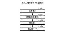
図2は、設計工程を説明する説明図である。より具体的には、図2は、図1に例示したシステムを用いてプリント板設計を行う設計工程を説明する図である。 FIG. 2 is an explanatory diagram for explaining the design process. More specifically, FIG. 2 is a diagram illustrating a design process for designing a printed board using the system illustrated in FIG.
図2に示すように、プリント板設計においては、先ず設計対象のプリント板に要求される仕様の検討が行われる(S1)。次いで、要求された仕様を満たすように、IC、トランジスタ等の各部品による回路図を作成するための論理(回路)設計が回路設計用のCAD等のエディッタ(以下、回路設計CAD)を用いて行われる(S2)。次いで、回路設計で作成された回路図の各部品について、基板上の搭載位置、配線位置、型番などを決める実装設計が実装設計用のCAD等のエディッタ(以下、実装設計CAD)を用いて行われる(S3)。次いで、設計対象のプリント板について、回路設計及び実装設計を経て決定された製造データを回路図DB1及び実装設計DB2より取得する(S4)。 As shown in FIG. 2, in the printed board design, first, the specification required for the printed board to be designed is examined (S1). Next, a logic (circuit) design for creating a circuit diagram of each component such as an IC and a transistor is used by using an editor such as a CAD for circuit design (hereinafter, circuit design CAD) so as to satisfy the required specifications. Performed (S2). Next, for each part of the circuit diagram created in the circuit design, mounting design for determining the mounting position, wiring position, model number, etc. on the board is performed using an editor such as a CAD for mounting design (hereinafter referred to as mounting design CAD). (S3). Next, for the printed circuit board to be designed, the manufacturing data determined through the circuit design and the mounting design is acquired from the circuit diagram DB1 and the mounting design DB2 (S4).
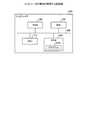
図3は、機能構成を例示するブロック図である。具体的には、図3は、図1に例示したシステムにおける、回路設計及び実装設計にかかる機能構成を例示する図である。 FIG. 3 is a block diagram illustrating a functional configuration. Specifically, FIG. 3 is a diagram illustrating a functional configuration related to circuit design and mounting design in the system illustrated in FIG.
図3に示すように、回路設計及び実装設計にかかる機能構成は、実装設計CAD10、バックアノテーション部20及び回路設計CAD30を有する。実装設計CAD10は、コンピュータ200などで実行されるプログラムであり、回路図の各部品について、基板上の搭載位置、配線位置、型番などをユーザの操作をもとに編集・決定する。 As illustrated in FIG. 3, the functional configuration related to circuit design and mounting design includes a
具体的には、実装設計CAD10は、編集対象とする回路のデータを回路図DB1より読み出し、モニタに回路図として表示する。次いで、実装設計CAD10は、回路図上の各部品について、GUI(Graphical User Interface)による操作(例えばマウスによる選択、指示など)をユーザより受け付けることで、実装設計にかかる編集・決定を行う。また、実装設計CAD10は、ユーザの指示によって実装設計について決定された情報を実装設計DB2へ登録する。また、実装設計CAD10は、実装設計について決定された情報の中に回路図DB1へ反映すべきバックアノテーション情報(以下、BA情報)がある場合、バックアノテーション部20を呼び出してBA情報を回路図DB1へ反映するバックアノテーションを依頼する。 Specifically, the
バックアノテーション部20は、コンピュータ200などで実行されるプログラムであり、例えば実装設計CAD10などにより呼び出されるAPI(Application Programming Interface)などである。バックアノテーション部20は、実装設計CAD10より依頼されたBA情報を回路図DB1へ反映するバックアノテーション処理(詳細は後述する)を実行する。 The back annotation unit 20 is a program executed by the
図4は、バックアノテーションを説明する説明図である。図4に示すように、回路図上のICなどの部品F1について、実装設計CAD10で決定された情報の中で、部品F1の搭載座標については回路図DB1へ反映すべきBA情報であるとする。実装設計CAD10は、実装設計DB2の項目の中で部品F1の搭載座標が決定された場合、その部品F1の搭載座標をBA情報とし、バックアノテーション部20に回路図DB1へのバックアノテーションを依頼する。なお、BA情報とする実装設計DB2の項目については、設定情報として予め設定されており、部品F1の搭載座標だけでなく、部品F1の品番などであってもよい。 FIG. 4 is an explanatory diagram for explaining the back annotation. As shown in FIG. 4, regarding the component F1 such as an IC on the circuit diagram, among the information determined by the mounting
回路設計CAD30は、コンピュータ200などで実行されるプログラムであり、設計対象の回路についての電気的、論理的な構成を示す回路図をユーザの操作をもとに編集・決定する。 The
具体的には、回路設計CAD30は、GUIによる操作(例えばマウスによる選択、指示など)をユーザより受け付けることで、回路設計にかかる編集・決定を行う。また、回路設計CAD30は、ユーザの指示によって回路設計について決定された情報を回路図DB1へ設定する。また、回路設計CAD30は、起動時や回路図DB1の編集時にログファイル3への書き込みを行うとともに、ログファイル3を逐次参照することで、複数起動している回路設計CAD30間の情報を共有する。具体的には、回路設計CAD30は、起動時/終了時に自身のタスクを識別するIDなどを、起動/終了を示す情報とともにログファイル3に記録する。また、回路設計CAD30は、編集対象としてロックし、他のCADによる編集が出来ないように排他的に編集している部品F1についての情報、回路図DB1への編集内容などをログファイル3に記録する。 Specifically, the
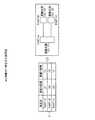
図5は、ログファイル3を例示する説明図である。図5に示すように、ログファイル3には、複数起動している回路設計CAD30ごとのタスクの情報が時系列順に逐次記録されている。回路設計CAD30は、ログファイル3を逐次参照することで、各タスクによる編集状態などを共有する。例えば、図示例では、「タスクA」、「タスクB」、「タスクC」の起動が記録されており、それぞれに終了の記録がないことから、「タスクA」、「タスクB」、「タスクC」が起動中であることがわかる。また、「タスクA」による「部品A」の追加配置と、「タスクB」による「部品B」の追加配置とが記録されていることから、追加配置された「部品A」、「部品B」の情報を「タスクA」、「タスクB」、「タスクC」間で共有できる。 FIG. 5 is an explanatory diagram illustrating the log file 3. As shown in FIG. 5, in the log file 3, task information for each activated
また、ログファイル3には、「タスクC」による「部品A」のロック及びロック解除が記録されている。したがって、「タスクC」による「部品A」のロックが記録された後の、ロック解除が記録されるまでの間は、「タスクC」によって「部品A」がロック中であることを、「タスクA」、「タスクB」、「タスクC」間で共有できる。 Further, the log file 3 records the locking and unlocking of “component A” by “task C”. Therefore, after the lock of “component A” by “task C” is recorded and before the unlocking is recorded, “task C” indicates that “component A” is locked. A "," task B ", and" task C "can be shared.
次に、バックアノテーション部20におけるバックアノテーション処理の詳細について説明する。図6は、バックアノテーション処理の一例を示すフローチャートである。 Next, details of the back annotation processing in the back annotation unit 20 will be described. FIG. 6 is a flowchart illustrating an example of back annotation processing.
図6に示すように、バックアノテーション部20は、実装設計CAD10などにより呼び出されて処理が開始されると、実装設計CAD10より依頼されたBA情報の読み込みと(S11)、回路図DB1の読み込みとを行う(S12)。 As shown in FIG. 6, when the back annotation unit 20 is called by the mounting
図7、8は、BA情報I1の一例を示す説明図である。より具体的には、図7はBA情報I1が部品F1の搭載座標である場合を示す図であり、図8はBA情報I1が部品F1の部品仕様、長さである場合を示す図である。図7、8に示すように、デバッグ・試験の際に回路図で不具合箇所を追跡するために回路図上に示すBA情報I1としては、部品F1の搭載座標(搭載位置)、部品仕様、長さなどがある。バックアノテーション部20は、実装設計CAD10などにより呼び出されて処理が開始されると、このBA情報I1を読み込む。 7 and 8 are explanatory diagrams showing an example of the BA information I1. More specifically, FIG. 7 is a diagram showing a case where the BA information I1 is the mounting coordinates of the component F1, and FIG. 8 is a diagram showing a case where the BA information I1 is the component specification and length of the component F1. . As shown in FIGS. 7 and 8, the BA information I1 shown on the circuit diagram in order to trace the failure location in the circuit diagram during debugging / testing includes the mounting coordinates (mounting position) of the component F1, the component specifications, and the length. There is. When the back annotation unit 20 is called by the mounting
次いで、バックアノテーション部20は、BA情報I1に含まれる部品F1ごとのループ処理(S13〜S19)を開始する。具体的には、図7の例では、「PART−A」、「PART−B」、「PART−C」ごとのループ処理が行われる。また、図8の例では、「コネクタA」、「コネクタB」、「ケーブルC」ごとのループ処理が行われる。 Next, the back annotation unit 20 starts a loop process (S13 to S19) for each component F1 included in the BA information I1. Specifically, in the example of FIG. 7, loop processing for each of “PART-A”, “PART-B”, and “PART-C” is performed. In the example of FIG. 8, loop processing is performed for each of “connector A”, “connector B”, and “cable C”.
バックアノテーション部20は、ループ処理が開始されると(S13)、ログファイル3を参照して現時点までの回路設計CAD30のログを読み込む(S14)。次いで、バックアノテーション部20は、読み込んだログをもとに、処理対象の部品F1が起動中の回路設計CAD30によってロックされているか否かを判定する(S15)。例えば、図5に例示したログファイル3では、「タスクA」、「タスクB」、「タスクC」のいずれかによって、処理対象の部品F1がロックされているか否かを判定する。 When the loop processing is started (S13), the back annotation unit 20 reads the log of the
ロックされていない場合(S15:NO)、バックアノテーション部20は、自身がBA情報I1を回路図DB1に設定する(S16)。具体的には、バックアノテーション部20は、回路図DB1において、BA情報I1を反映する回路と同一の識別子を有する回路の項目に、BA情報I1の内容を設定する。 If not locked (S15: NO), the back annotation unit 20 itself sets the BA information I1 in the circuit diagram DB1 (S16). Specifically, the back annotation unit 20 sets the content of the BA information I1 in the circuit item having the same identifier as the circuit reflecting the BA information I1 in the circuit diagram DB1.
これにより、処理対象の部品F1がロックされていない場合には、バックアノテーション部20がBA情報I1を素早く回路図DB1に反映できる。また、部品F1ごとにループ処理が行われることから、他の部品F1のロックの有無に関係なく、BA情報I1の回路図DB1への反映を行うことができる。 Thereby, when the component F1 to be processed is not locked, the back annotation unit 20 can quickly reflect the BA information I1 in the circuit diagram DB1. Further, since loop processing is performed for each component F1, the BA information I1 can be reflected in the circuit diagram DB1 regardless of whether other components F1 are locked.
次いで、バックアノテーション部20は、回路図DB1にBA情報I1を設定したことを示す通常ログをログファイル3に出力する(S17)。具体的には、バックアノテーション部20は、部品F1についてBA情報I1を設定したことをログファイル3に記述する。これにより、起動中の回路設計CAD30は、バックアノテーション部20によって回路図DB1にBA情報I1が設定されたことを共有できる。 Next, the back annotation unit 20 outputs a normal log indicating that the BA information I1 is set in the circuit diagram DB1 to the log file 3 (S17). Specifically, the back annotation unit 20 describes in the log file 3 that the BA information I1 has been set for the component F1. Thereby, the
ロックされている場合(S15:YES)、バックアノテーション部20は、ロックしている回路設計CAD30に対してBA情報I1のバックアノテーションを依頼する依頼ログをログファイル3に出力する(S18)。具体的には、バックアノテーション部20は、ロックしている回路設計CAD30を依頼先とし、BA情報I1を回路図DB1へ反映する依頼内容のログをログファイル3に記述する。これにより、依頼先とされた回路設計CAD30では、自身がロックしている部品F1についてのBA情報I1を回路図DB1へ反映することができる。 When locked (S15: YES), the back annotation unit 20 outputs a request log for requesting the back annotation of the BA information I1 to the locked
バックアノテーション部20は、上述したS14〜S18の処理を、BA情報I1に含まれる部品F1の全てについて行ったところで、ループ処理を終了する(S19)。これにより、BA情報I1に含まれる全ての部品F1について、バックアノテーションを行うことができる。 The back annotation unit 20 ends the loop process when the processes of S14 to S18 described above are performed for all the components F1 included in the BA information I1 (S19). Thereby, back annotation can be performed about all the components F1 contained in BA information I1.
次に、回路設計CAD30における処理の詳細について説明する。図9は、回路設計CAD30の処理の一例を示すフローチャートである。図9に示すように、回路設計CAD30の起動指示などによって処理が開始されると、回路設計CAD30は、回路図DB1と、ログファイル3との読み込みを行う(S21、S22)。 Next, details of processing in the
次いで、回路設計CAD30は、ログファイル3に記述された他の回路設計CAD30の状態(起動の有無、編集内容など)、バックアノテーション部20が行ったバックアノテーションの内容などの通常ログをメモリに展開して最新の情報に反映する(S23)。これにより、回路設計CAD30における回路図上の表記などが、ログファイル3に記述された最新の内容に更新されることとなる。 Next, the
次いで、回路設計CAD30は、ログファイル3に記述されたログの中に、BA情報I1のバックアノテーションを依頼する依頼ログがあるか否かを判定する(S24)。依頼ログがない場合(S24:NO)、回路設計CAD30はS28へ処理を進める。 Next, the
依頼ログがある場合(S24:YES)、回路設計CAD30は自身が依頼ログの依頼先であるか否かを判定する(S25)。例えば、ログファイル3上における自身を示すIDが「タスクA」である場合、依頼ログの依頼先が「タスクA」であるか否かを判定する。依頼先でない場合(S25:NO)、回路設計CAD30は、依頼ログに記述された依頼内容については何もせず、S28へ処理を進める。 When there is a request log (S24: YES), the
依頼先である場合(S25:YES)、回路設計CAD30は、依頼ログをもとにBA情報I1を回路図DB1に設定し(S26)、回路図DB1にBA情報I1を設定したことを示す通常ログをログファイル3に出力する(S27)。これにより、依頼先とされた回路設計CAD30では、自身がロックしている部品F1についてのBA情報I1を回路図DB1へ反映する。 If it is the request destination (S25: YES), the
S28において、回路設計CAD30は、マウス・キーボードなどの入力デバイスからのイベント処理を受け付けて、イベント処理による受け付けられたコマンドが実行可能なコマンドであるか否かを判定する(S29)。 In S28, the
具体的には、S29では、回路設計において実行可能なコマンド以外のコマンドがイベント処理で受け付けられたか否かを判定する。例えば、部品F1の選択、移動などのコマンドは、回路設計において実行できるコマンドとして判定される。また、部品F1の品番変更などは、回路設計ではなく実装設計において実行可能なコマンドであることから、回路設計において実行できないコマンドとして判定される。実行可能なコマンドでない場合(S29:NO)、回路設計CAD30は、S22へと処理を戻し、次のイベント処理の受け付けを行う。 Specifically, in S29, it is determined whether or not a command other than a command that can be executed in circuit design has been accepted in the event processing. For example, commands such as selection and movement of the component F1 are determined as commands that can be executed in circuit design. Further, the change of the part number of the component F1 is determined as a command that cannot be executed in the circuit design because it is a command that can be executed in the mounting design, not the circuit design. If it is not an executable command (S29: NO), the
実行可能なコマンドである場合(S29:YES)、回路設計CAD30は、ログファイル3を読み込み(S30)、他のタスクによるロック要素の読み込み、すなわち他の回路設計CAD30がロックしている部品F1の情報を読み込む(S31)。 When the command is an executable command (S29: YES), the
次いで、回路設計CAD30は、コマンドの処理対象要素である部品F1が他の回路設計CAD30によりロックされているか否かを判定する(S32)。ロックされている場合(S32:YES)、回路設計CAD30は、他の回路設計CAD30によりロックされており、コマンドが実行できない(コマンドキャンセル)のメッセージ通知をモニタなどに行う(S33)。 Next, the
ロックされていない場合(S32:NO)、回路設計CAD30は、ログファイル3にコマンドの処理対象要素である部品F1をロック要素とすることを書き込む(S34)。具体的には、コマンドの処理対象となった部品F1をロックすることをログファイル3に記述する。これにより、コマンドの処理対象となった部品F1がロック中であることを、他の回路設計CAD30やバックアノテーション部20などに通知できる。 If not locked (S32: NO), the
次いで、回路設計CAD30は、受け付けたコマンドを実行し(S35)、コマンドの実行により新たに反映された編集内容をログファイル3に書き込む(S36)。これにより、新たに反映された編集内容を他の回路設計CAD30などと共有することができる。 Next, the
次いで、回路設計CAD30は、自身のタスクを終了するコマンドの入力の有無を判定する(S37)。終了するコマンドの入力がなかった場合(S37:NO)、回路設計CAD30はS22へ処理を戻す。終了するコマンドの入力があった場合(S37:YES)、回路設計CAD30は処理を終了する。 Next, the
[変形例1]
次に、上述した実施形態の変形例1を説明する。変形例1は、処理対象の部品F1がロックされていない場合であっても、バックアノテーション部20自身がBA情報I1を反映することなく、任意のタスクにBA情報I1の反映を依頼する点が上述した実施形態とは異なる。[Modification 1]
Next,
図10は、変形例1にかかるバックアノテーション処理の一例を示すフローチャートである。図10に示すように、処理対象の部品F1がロックされていない場合(S15:NO)、バックアノテーション部20は、任意の回路設計CAD30(タスク)に対してBA情報I1のバックアノテーションを依頼する依頼ログをログファイル3に出力する(S18a)。なお、任意のタスクの指定については、起動中であるタスクであればいずれのタスクであってもよく、例えばランダム方式やラウンドロビン方式でいずれかのタスクを指定してもよい。これにより、依頼先とされた任意の回路設計CAD30において、部品F1についてのBA情報I1を回路図DB1へ反映することができる。 FIG. 10 is a flowchart illustrating an example of the back annotation process according to the first modification. As shown in FIG. 10, when the processing target component F1 is not locked (S15: NO), the back annotation unit 20 requests the back annotation of the BA information I1 from an arbitrary circuit design CAD 30 (task). The request log is output to the log file 3 (S18a). Note that any task may be specified as long as it is an active task. For example, any task may be specified in a random method or a round robin method. As a result, the BA information I1 for the component F1 can be reflected in the circuit diagram DB1 in the arbitrary
また、ロックされている場合(S15:YES)、バックアノテーション部20は、ロックしている回路設計CAD30(タスク)に対してBA情報I1のバックアノテーションを依頼する依頼ログをログファイル3に出力する(S18b)。 If it is locked (S15: YES), the back annotation unit 20 outputs to the log file 3 a request log for requesting the back annotation of the BA information I1 to the locked circuit design CAD 30 (task). (S18b).
[変形例2]
次に、上述した実施形態の変形例2を説明する。変形例2は、自身がBA情報I1を反映することなく、BA情報I1の反映を全タスク宛に依頼する点が上述した実施形態とは異なる。[Modification 2]
Next,
図11は、変形例2にかかるバックアノテーション処理の一例を示すフローチャートである。図11に示すように、バックアノテーション部20は、実装設計CAD10などにより呼び出されて処理が開始されると、実装設計CAD10より依頼されたBA情報I1の読み込みと(S11)、回路図DB1の読み込みとを行う(S12)。 FIG. 11 is a flowchart illustrating an example of back annotation processing according to the second modification. As shown in FIG. 11, when the back annotation unit 20 is called by the mounting
次いで、バックアノテーション部20は、ログファイル3を参照して現時点までの回路設計CAD30のログを読み込み(S13)、起動中の全タスクに対して、BA情報I1のバックアノテーションを依頼する依頼ログをログファイル3に出力する(S17b)。これにより、バックアノテーション部20は、自身がBA情報I1を反映することなく、BA情報I1の反映を全タスクに依頼する。 Next, the back annotation unit 20 reads the log of the
図12は、変形例2にかかる回路設計CAD30の処理の一例を示すフローチャートである。図12に示すように、変形例2では、S24において依頼ログがあると判定された場合(S24:YES)以後の処理の内容が上述した実施形態とは異なっている。 FIG. 12 is a flowchart illustrating an example of processing of the
具体的には、依頼ログがある場合(S24:YES)、回路設計CAD30は、依頼ログのBA情報I1に含まれる部品F1ごとのループ処理(S40〜S46)を開始する。 Specifically, when there is a request log (S24: YES), the
ループ処理が開始されると(S40)、回路設計CAD30は、処理対象要素である部品F1は起動中の回路設計CAD30によってロックされているか否かを判定する(S41)。ロックされていない場合(S41:NO)、回路設計CAD30は、自身がBA情報I1を回路図DB1に設定する(S42)。 When the loop process is started (S40), the
ロックされている場合(S41:YES)、回路設計CAD30は、自身が部品F1をロック中であるか否かを判定する(S43)。自身がロック中でない場合(S43:NO)、他の回路設計CAD30(タスク)がロック中であることから、回路設計CAD30は何もせずにS46へ処理を進める。 When locked (S41: YES), the
自身がロック中である場合(S43:YES)、回路設計CAD30は、自身がBA情報I1を回路図DB1に設定し(S44)、通常ログをログファイル3に出力する(S45)。 If it is locked (S43: YES), the
回路設計CAD30は、上述したS40〜S45の処理を、BA情報I1に含まれる部品F1の全てについて行ったところで、ループ処理を終了する(S46)。これにより、全タスク宛に依頼されたBA情報I1に含まれる全ての部品F1について、バックアノテーションを行うことができる。 The
また、上記の実施形態で説明した各種の処理は、あらかじめ用意されたプログラムをパーソナルコンピュータやワークステーションなどのコンピュータ200で実行することによって実現することもできる。そこで、以下では、上記の実施形態と同様の機能を有するプログラムを実行するコンピュータ200の構成を説明する。図13は、コンピュータの構成を説明する説明図である。 The various processes described in the above embodiments can also be realized by executing a program prepared in advance on a
図13に示すように、コンピュータ200は、CPU210、ROM(Read Only Memory)220、HDD(Hard Disk Drive)230、RAM(Random Access Memory)240を有する。これら210〜240の各部は、バス400を介して接続される。 As illustrated in FIG. 13, the
ROM220には上記の実装設計CAD10、バックアノテーション部20、回路設計CAD30と同様の機能を発揮するプログラム220aが予め記憶される。なお、プログラム220aについては、実装設計CAD10、バックアノテーション部20、回路設計CAD30ごとに適宜分離してもよい。 The
そして、CPU210が、プログラム220aをROM220から読み出して実行することで、実装設計CAD10、バックアノテーション部20、回路設計CAD30と同様の動作を実行する。 Then, the
なお、プログラム220aについては、必ずしも最初からROM220に記憶させることを要しない。例えば、コンピュータ200に挿入されるフレキシブルディスク(FD)、CD−ROM、DVDディスク、光磁気ディスク、ICカードなどの「可搬用の物理媒体」にプログラムを記憶させておく。そして、コンピュータ200がこれらからプログラムを読み出して実行するようにしてもよい。 The
さらには、公衆回線、インターネット、LAN、WAN(Wide Area Network)などを介してコンピュータ200に接続される「他のコンピュータ(またはサーバ)」などにプログラムを記憶させておく。そして、コンピュータ200がこれらからプログラムを読み出して実行するようにしてもよい。 Furthermore, the program is stored in “another computer (or server)” connected to the
1…回路図DB
2…実装設計DB
3…ログファイル
10…実装設計CAD
20…バックアノテーション部
30…回路設計CAD
100…サーバ装置
200…コンピュータ
F1…部品
I1…BA情報
N…通信ネットワーク1 ... Circuit diagram DB
2 ... Mounting design DB
3 ... Log
20 ...
DESCRIPTION OF
Claims (5)
Translated fromJapanese第1の工程で決定された情報を前記第1の工程よりも前の第2の工程に関する情報に反映させるバックアノテーション処理を、前記第2の工程にかかるエディッタの動作に関するログファイルに基づいて、前記第1の工程で決定された情報にかかる部品が前記エディッタによりロックされている場合、起動中の前記エディッタに依頼し、ロックされていない場合、自装置で行う、
処理を実行させることを特徴とする情報処理プログラム。On the computer,
Based on the log file relating to the operation of the editor relating to the second step, the back annotation process for reflecting the information determined in the first step to the information relating to the second step prior to the first step, If the part related to the information determined in the first step is locked by the editor, ask the active editor to start.
An information processing program for executing a process.
前記ロックされている場合、当該バックアノテーション処理により反映させる情報を前記ログファイルに出力する
請求項1に記載の情報処理プログラム。The back annotation process includes
The information processing program according to claim 1, wherein when locked, the information reflected by the back annotation processing is output to the log file.
前記ロックされていない場合、当該バックアノテーション処理により反映させた情報を前記ログファイルに出力する
請求項1又は2に記載の情報処理プログラム。The back annotation process includes
3. The information processing program according to claim 1, wherein, when the information is not locked, the information reflected by the back annotation processing is output to the log file.
を有することを特徴とする情報処理装置。Based on the log file relating to the operation of the editor relating to the second step, the back annotation process for reflecting the information determined in the first step to the information relating to the second step prior to the first step, When the part related to the information determined in the first step is locked by the editor, the editor is requested to be activated, and when not locked, the component has a back annotation processing unit to be performed by the own device. A characteristic information processing apparatus.
第1の工程で決定された情報を前記第1の工程よりも前の第2の工程に関する情報に反映させるバックアノテーション処理を、前記第2の工程にかかるエディッタの動作に関するログファイルに基づいて、前記第1の工程で決定された情報にかかる部品が前記エディッタによりロックされている場合、起動中の前記エディッタに依頼し、ロックされていない場合、自装置で行う
処理を実行することを特徴とするバックアノテーション方法。Computer
Based on the log file relating to the operation of the editor relating to the second step, the back annotation process for reflecting the information determined in the first step to the information relating to the second step prior to the first step, When the part related to the information determined in the first step is locked by the editor, the active editor is requested, and when the part is not locked, the processing performed by the own device is executed. Back annotation method to do.
Priority Applications (2)
| Application Number | Priority Date | Filing Date | Title |
|---|---|---|---|
| JP2014088529AJP2015207218A (en) | 2014-04-22 | 2014-04-22 | Information processing program, information processing apparatus, and back annotation method |
| US14/632,156US20150302131A1 (en) | 2014-04-22 | 2015-02-26 | Information processing apparatus and back annotation method |
Applications Claiming Priority (1)
| Application Number | Priority Date | Filing Date | Title |
|---|---|---|---|
| JP2014088529AJP2015207218A (en) | 2014-04-22 | 2014-04-22 | Information processing program, information processing apparatus, and back annotation method |
Publications (1)
| Publication Number | Publication Date |
|---|---|
| JP2015207218Atrue JP2015207218A (en) | 2015-11-19 |
Family
ID=54322217
Family Applications (1)
| Application Number | Title | Priority Date | Filing Date |
|---|---|---|---|
| JP2014088529AWithdrawnJP2015207218A (en) | 2014-04-22 | 2014-04-22 | Information processing program, information processing apparatus, and back annotation method |
Country Status (2)
| Country | Link |
|---|---|
| US (1) | US20150302131A1 (en) |
| JP (1) | JP2015207218A (en) |
Families Citing this family (1)
| Publication number | Priority date | Publication date | Assignee | Title |
|---|---|---|---|---|
| CN109885853A (en)* | 2018-11-22 | 2019-06-14 | 北京华大九天软件有限公司 | A kind of full example reactionary slogan, anti-communist poster method of level DRC verification result |
Family Cites Families (7)
| Publication number | Priority date | Publication date | Assignee | Title |
|---|---|---|---|---|
| US6115034A (en)* | 1997-01-31 | 2000-09-05 | Canon Kabushiki Kaisha | Step managing apparatus and method |
| US6353817B1 (en)* | 1998-06-26 | 2002-03-05 | Charles M Jacobs | Multi-user system for creating and maintaining a medical-decision-making knowledge base |
| JP4031905B2 (en)* | 2000-11-09 | 2008-01-09 | 富士通株式会社 | Circuit design apparatus and circuit design method |
| US20020199173A1 (en)* | 2001-01-29 | 2002-12-26 | Matt Bowen | System, method and article of manufacture for a debugger capable of operating across multiple threads and lock domains |
| US20030145310A1 (en)* | 2001-10-31 | 2003-07-31 | Metacyber. Net. | Computer memory structure for storing original source information and associated interpretative information |
| US7784006B1 (en)* | 2006-07-27 | 2010-08-24 | Xilinx, Inc. | Method and apparatus for directed physical implementation of a circuit design for an integrated circuit |
| US8364656B2 (en)* | 2008-10-31 | 2013-01-29 | Cadence Design Systems, Inc. | Method and system for implementing multiuser cached parameterized cells |
- 2014
- 2014-04-22JPJP2014088529Apatent/JP2015207218A/ennot_activeWithdrawn
- 2015
- 2015-02-26USUS14/632,156patent/US20150302131A1/ennot_activeAbandoned
Also Published As
| Publication number | Publication date |
|---|---|
| US20150302131A1 (en) | 2015-10-22 |
Similar Documents
| Publication | Publication Date | Title |
|---|---|---|
| US9740594B2 (en) | Automated debug trace specification | |
| US8510712B1 (en) | Testing in-container software objects | |
| CN113238850B (en) | RPA realization method, device, equipment and medium based on browser | |
| US20130117738A1 (en) | Server Upgrades with Safety Checking and Preview | |
| CN110727581B (en) | Crash location method and electronic device | |
| CN111736930A (en) | Program front-back end interface calling method and device, computer equipment and storage medium | |
| EP2435912B1 (en) | Controlling a running application for live scene graph editing | |
| US20140258785A1 (en) | Identifying a storage location for a storage address requested during debugging | |
| JP6942277B1 (en) | Security test system | |
| JP2015207218A (en) | Information processing program, information processing apparatus, and back annotation method | |
| CN118363846A (en) | Test method and device | |
| CN113535590B (en) | Program testing method and device | |
| US10146529B2 (en) | Monitoring rules declaration and automatic configuration of the monitoring rules | |
| JP7277694B2 (en) | Information processing device, its control method and program | |
| JP2012048660A (en) | Static analysis processing system, method, and program | |
| CN119759472B (en) | Single page application routing method, device, computer equipment and storage medium | |
| US20250004757A1 (en) | Version management and releases of a software application | |
| US20250004758A1 (en) | Software application execution using contextual information | |
| CN114579344B (en) | A salt-stack-based configuration and verification system and method | |
| US9626228B1 (en) | Synchronizing stateless process across multiple instances | |
| JP7311740B2 (en) | Information processing system, its control method, and program | |
| JP2007018091A (en) | Information processing apparatus, information processing system, application development support method, and program | |
| JP2017049675A (en) | Fault reproduction system and fault reproduction method | |
| JP2008052410A (en) | Computer development equipment | |
| JP6369333B2 (en) | Software installation determination program, software installation determination method, and software installation determination device |
Legal Events
| Date | Code | Title | Description |
|---|---|---|---|
| A621 | Written request for application examination | Free format text:JAPANESE INTERMEDIATE CODE: A621 Effective date:20170110 | |
| A761 | Written withdrawal of application | Free format text:JAPANESE INTERMEDIATE CODE: A761 Effective date:20170220 |