JP2015197543A - Mounting board and electronic equipment - Google Patents
Mounting board and electronic equipmentDownload PDFInfo
- Publication number
- JP2015197543A JP2015197543AJP2014074842AJP2014074842AJP2015197543AJP 2015197543 AJP2015197543 AJP 2015197543AJP 2014074842 AJP2014074842 AJP 2014074842AJP 2014074842 AJP2014074842 AJP 2014074842AJP 2015197543 AJP2015197543 AJP 2015197543A
- Authority
- JP
- Japan
- Prior art keywords
- pixel
- wiring
- signal
- substrate
- mounting
- Prior art date
- Legal status (The legal status is an assumption and is not a legal conclusion. Google has not performed a legal analysis and makes no representation as to the accuracy of the status listed.)
- Pending
Links
Images


Classifications
- G—PHYSICS
- G09—EDUCATION; CRYPTOGRAPHY; DISPLAY; ADVERTISING; SEALS
- G09G—ARRANGEMENTS OR CIRCUITS FOR CONTROL OF INDICATING DEVICES USING STATIC MEANS TO PRESENT VARIABLE INFORMATION
- G09G3/00—Control arrangements or circuits, of interest only in connection with visual indicators other than cathode-ray tubes
- G09G3/20—Control arrangements or circuits, of interest only in connection with visual indicators other than cathode-ray tubes for presentation of an assembly of a number of characters, e.g. a page, by composing the assembly by combination of individual elements arranged in a matrix no fixed position being assigned to or needed to be assigned to the individual characters or partial characters
- G09G3/22—Control arrangements or circuits, of interest only in connection with visual indicators other than cathode-ray tubes for presentation of an assembly of a number of characters, e.g. a page, by composing the assembly by combination of individual elements arranged in a matrix no fixed position being assigned to or needed to be assigned to the individual characters or partial characters using controlled light sources
- G09G3/30—Control arrangements or circuits, of interest only in connection with visual indicators other than cathode-ray tubes for presentation of an assembly of a number of characters, e.g. a page, by composing the assembly by combination of individual elements arranged in a matrix no fixed position being assigned to or needed to be assigned to the individual characters or partial characters using controlled light sources using electroluminescent panels
- G09G3/32—Control arrangements or circuits, of interest only in connection with visual indicators other than cathode-ray tubes for presentation of an assembly of a number of characters, e.g. a page, by composing the assembly by combination of individual elements arranged in a matrix no fixed position being assigned to or needed to be assigned to the individual characters or partial characters using controlled light sources using electroluminescent panels semiconductive, e.g. using light-emitting diodes [LED]
- G—PHYSICS
- G09—EDUCATION; CRYPTOGRAPHY; DISPLAY; ADVERTISING; SEALS
- G09G—ARRANGEMENTS OR CIRCUITS FOR CONTROL OF INDICATING DEVICES USING STATIC MEANS TO PRESENT VARIABLE INFORMATION
- G09G3/00—Control arrangements or circuits, of interest only in connection with visual indicators other than cathode-ray tubes
- G09G3/20—Control arrangements or circuits, of interest only in connection with visual indicators other than cathode-ray tubes for presentation of an assembly of a number of characters, e.g. a page, by composing the assembly by combination of individual elements arranged in a matrix no fixed position being assigned to or needed to be assigned to the individual characters or partial characters
- G09G3/2085—Special arrangements for addressing the individual elements of the matrix, other than by driving respective rows and columns in combination
- G—PHYSICS
- G09—EDUCATION; CRYPTOGRAPHY; DISPLAY; ADVERTISING; SEALS
- G09G—ARRANGEMENTS OR CIRCUITS FOR CONTROL OF INDICATING DEVICES USING STATIC MEANS TO PRESENT VARIABLE INFORMATION
- G09G2300/00—Aspects of the constitution of display devices
- G09G2300/02—Composition of display devices
- G09G2300/026—Video wall, i.e. juxtaposition of a plurality of screens to create a display screen of bigger dimensions
- G—PHYSICS
- G09—EDUCATION; CRYPTOGRAPHY; DISPLAY; ADVERTISING; SEALS
- G09G—ARRANGEMENTS OR CIRCUITS FOR CONTROL OF INDICATING DEVICES USING STATIC MEANS TO PRESENT VARIABLE INFORMATION
- G09G2300/00—Aspects of the constitution of display devices
- G09G2300/04—Structural and physical details of display devices
- G09G2300/0404—Matrix technologies
- G09G2300/0408—Integration of the drivers onto the display substrate
- G—PHYSICS
- G09—EDUCATION; CRYPTOGRAPHY; DISPLAY; ADVERTISING; SEALS
- G09G—ARRANGEMENTS OR CIRCUITS FOR CONTROL OF INDICATING DEVICES USING STATIC MEANS TO PRESENT VARIABLE INFORMATION
- G09G2300/00—Aspects of the constitution of display devices
- G09G2300/04—Structural and physical details of display devices
- G09G2300/0421—Structural details of the set of electrodes
- G09G2300/0426—Layout of electrodes and connections
- G—PHYSICS
- G09—EDUCATION; CRYPTOGRAPHY; DISPLAY; ADVERTISING; SEALS
- G09G—ARRANGEMENTS OR CIRCUITS FOR CONTROL OF INDICATING DEVICES USING STATIC MEANS TO PRESENT VARIABLE INFORMATION
- G09G2310/00—Command of the display device
- G09G2310/02—Addressing, scanning or driving the display screen or processing steps related thereto
- G09G2310/0264—Details of driving circuits
- G09G2310/0294—Details of sampling or holding circuits arranged for use in a driver for data electrodes
- G—PHYSICS
- G09—EDUCATION; CRYPTOGRAPHY; DISPLAY; ADVERTISING; SEALS
- G09G—ARRANGEMENTS OR CIRCUITS FOR CONTROL OF INDICATING DEVICES USING STATIC MEANS TO PRESENT VARIABLE INFORMATION
- G09G2310/00—Command of the display device
- G09G2310/08—Details of timing specific for flat panels, other than clock recovery
- G—PHYSICS
- G09—EDUCATION; CRYPTOGRAPHY; DISPLAY; ADVERTISING; SEALS
- G09G—ARRANGEMENTS OR CIRCUITS FOR CONTROL OF INDICATING DEVICES USING STATIC MEANS TO PRESENT VARIABLE INFORMATION
- G09G2360/00—Aspects of the architecture of display systems
- G09G2360/14—Detecting light within display terminals, e.g. using a single or a plurality of photosensors
- G09G2360/141—Detecting light within display terminals, e.g. using a single or a plurality of photosensors the light conveying information used for selecting or modulating the light emitting or modulating element
- G09G2360/142—Detecting light within display terminals, e.g. using a single or a plurality of photosensors the light conveying information used for selecting or modulating the light emitting or modulating element the light being detected by light detection means within each pixel
- G—PHYSICS
- G09—EDUCATION; CRYPTOGRAPHY; DISPLAY; ADVERTISING; SEALS
- G09G—ARRANGEMENTS OR CIRCUITS FOR CONTROL OF INDICATING DEVICES USING STATIC MEANS TO PRESENT VARIABLE INFORMATION
- G09G3/00—Control arrangements or circuits, of interest only in connection with visual indicators other than cathode-ray tubes
- G09G3/20—Control arrangements or circuits, of interest only in connection with visual indicators other than cathode-ray tubes for presentation of an assembly of a number of characters, e.g. a page, by composing the assembly by combination of individual elements arranged in a matrix no fixed position being assigned to or needed to be assigned to the individual characters or partial characters
- G09G3/2085—Special arrangements for addressing the individual elements of the matrix, other than by driving respective rows and columns in combination
- G09G3/2088—Special arrangements for addressing the individual elements of the matrix, other than by driving respective rows and columns in combination with use of a plurality of processors, each processor controlling a number of individual elements of the matrix
- H—ELECTRICITY
- H10—SEMICONDUCTOR DEVICES; ELECTRIC SOLID-STATE DEVICES NOT OTHERWISE PROVIDED FOR
- H10K—ORGANIC ELECTRIC SOLID-STATE DEVICES
- H10K59/00—Integrated devices, or assemblies of multiple devices, comprising at least one organic light-emitting element covered by group H10K50/00
- H10K59/10—OLED displays
- H10K59/18—Tiled displays
Landscapes
- Engineering & Computer Science (AREA)
- Physics & Mathematics (AREA)
- Computer Hardware Design (AREA)
- General Physics & Mathematics (AREA)
- Theoretical Computer Science (AREA)
- Devices For Indicating Variable Information By Combining Individual Elements (AREA)
- Control Of El Displays (AREA)
- Control Of Indicators Other Than Cathode Ray Tubes (AREA)
- Electroluminescent Light Sources (AREA)
- Transforming Light Signals Into Electric Signals (AREA)
Abstract
Translated fromJapaneseDescription
Translated fromJapanese本技術は、配線基板上に駆動部を有する実装基板、およびそれを備えた電子機器に関する。 The present technology relates to a mounting board having a drive unit on a wiring board, and an electronic apparatus including the mounting board.
表示画素を選択する駆動部を実装する手法として、COG(Chip on Glass)やCOF(Chip On Film)が知られている(例えば特許文献1,2参照)。 COG (Chip on Glass) and COF (Chip On Film) are known as methods for mounting a drive unit for selecting display pixels (see, for example,
COGを用いた場合には、実装基板の上面端部に、FPCの接続端子を実装するスペースを設けることが必要となる。COFを用いた場合には、実装基板の上面端部に、駆動部を実装するスペースを設けることが必要となる。そのため、いずれの手法を用いた場合であっても、実装基板の上面端部にスペースが必要となるので、表示画素の配置できない額縁領域を設けることが必要となる。しかし、そのような額縁領域を設けた場合に、複数の実装基板をタイリングしたときには、表示映像に目地がくっきりと発生してしまうという問題があった。 When COG is used, it is necessary to provide a space for mounting the connection terminal of the FPC at the upper end portion of the mounting substrate. When COF is used, it is necessary to provide a space for mounting the drive unit at the upper surface end of the mounting substrate. For this reason, in any case, since a space is required at the upper end of the mounting substrate, it is necessary to provide a frame area where display pixels cannot be arranged. However, when such a frame region is provided, when a plurality of mounting boards are tiled, there is a problem that joints are clearly generated in a display image.
なお、このような問題は、表示装置の分野だけでなく、照明装置や受光装置の分野においても生じ得る。 Such a problem may occur not only in the field of display devices but also in the fields of illumination devices and light receiving devices.
本技術はかかる問題点に鑑みてなされたもので、その目的は、複数の実装基板をタイリングしたときに目地をより目立たなくすることの可能な実装基板およびそれを備えた電子機器を提供することにある。 The present technology has been made in view of such problems, and an object of the present technology is to provide a mounting board capable of making the joints less noticeable when tiling a plurality of mounting boards and an electronic apparatus including the mounting board. There is.
本技術の実装基板は、配線基板と、配線基板の画素領域に行列状に配置された複数の画素と、画素領域に配置され、複数の画素を複数個ずつ選択する複数の駆動部とを備えている。各画素は、発光もしくは受光する光素子と、光素子の発光もしくは受光を制御する画素回路とを含んでいる。複数の駆動部は、1画素行ごと、もしくは複数画素行ごとに、1つずつ、もしくは複数ずつ割り当てられている。 A mounting substrate of the present technology includes a wiring substrate, a plurality of pixels arranged in a matrix in the pixel region of the wiring substrate, and a plurality of driving units arranged in the pixel region and selecting a plurality of pixels one by one. ing. Each pixel includes an optical element that emits or receives light and a pixel circuit that controls light emission or reception of the optical element. The plurality of driving units are assigned to each pixel row or to each pixel row one or more.
本技術の電子機器は、1または複数の上記実装基板と、1または複数の上記実装基板を制御する制御回路とを備えている。 The electronic device of the present technology includes one or more mounting boards and a control circuit that controls the one or more mounting boards.
本技術の実装基板および電子機器では、複数の駆動部が、画素領域に配置されており、さらに、1画素行ごと、もしくは複数画素行ごとに、1つずつ、もしくは複数ずつ割り当てられている。これにより、複数の駆動部を、実装基板の上面端部に設けたり、複数の駆動部を実装したFPCの接続端子を実装基板の上面端部に設けたりする必要がなくなる。 In the mounting substrate and the electronic device of the present technology, the plurality of driving units are arranged in the pixel region, and are assigned one or more for each pixel row or for each of the plurality of pixel rows. This eliminates the need to provide a plurality of driving units at the upper surface end of the mounting substrate, or to provide connection terminals of the FPC on which the plurality of driving units are mounted at the upper surface end of the mounting substrate.
本技術の実装基板および電子機器によれば、複数の駆動部を、画素領域に配置するとともに、1画素行ごと、もしくは複数画素行ごとに、1つずつ、もしくは複数ずつ割り当てるようにしたので、複数の実装基板をタイリングしたときに目地をより目立たなくすることができる。なお、ここに記載された効果は必ずしも限定されるものではなく、本開示中に記載されたいずれの効果であってもよい。 According to the mounting substrate and the electronic apparatus of the present technology, the plurality of driving units are arranged in the pixel region and are assigned to each pixel row or to each pixel row one by one or more, The joint can be made less conspicuous when a plurality of mounting boards are tiled. Note that the effects described here are not necessarily limited, and may be any effects described in the present disclosure.
以下、本技術を実施するための形態について、図面を参照して詳細に説明する。なお、説明は以下の順序で行う。
1.第1の実施の形態(表示装置)
2.変形例(表示装置)
3.第2の実施の形態(照明装置)
4.第3の実施の形態(受光装置)
5.各実施の形態に共通の変形例
Hereinafter, modes for carrying out the present technology will be described in detail with reference to the drawings. The description will be given in the following order.
1. First embodiment (display device)
2. Modified example (display device)
3. Second embodiment (lighting device)
4). Third embodiment (light receiving device)
5. Modification common to each embodiment
<1.第1の実施の形態>
[構成]
図1は、本技術の第1の実施の形態に係る表示装置1の斜視構成の一例を表す。表示装置1は、いわゆるLEDディスプレイと呼ばれるものであり、表示画素としてLEDが用いられたものである。表示装置1は、例えば、図1に示したように、表示パネルモジュール10と、表示パネルモジュール10(具体的には後述の複数のセル12E)を制御するコントローラ20とを備えている。表示パネルモジュール10は、例えば、表示パネル12と、表示パネル12の周囲に設けられた回路(ソースドライバ13、ゲートドライバ14)とを有している。セル12Eが、本技術の「実装基板」の一具体例に相当する。コントローラ20が、本技術の「制御回路」の一具体例に相当する。<1. First Embodiment>
[Constitution]
FIG. 1 illustrates an example of a perspective configuration of the
(表示パネル12)
表示パネル12は、複数の画素11が表示パネル12の画素領域12a全面に渡って行列状に配置されたものである。画素11が、本技術の「画素」の一具体例に相当する。画素領域12aは、表示パネル12において映像表示が行われる領域(表示領域)に相当する。表示パネル12は、コントローラ20によって各画素11がアクティブマトリクス駆動されることにより、映像信号Vsig1〜VsigNに基づく映像を表示領域に表示する。映像信号Vsig1〜VsigNは、相展開した映像信号である。(Display panel 12)
The
表示パネル12は、行方向に延在する複数のゲート線Gateと、列方向に延在する複数のデータ線Sigとを有している。データ線Sigが、本技術の「信号線」の一具体例に相当する。ゲート線Gateが、本技術の「選択線」の一具体例に相当する。データ線Sigとゲート線Gateとの交差部分に対応して画素11が設けられている。各データ線Sigは、ソースドライバ13の出力端に接続されている。各ゲート線Gateは、ゲートドライバ14の出力端に接続されている。 The
図2は、表示パネル12の斜視構成の一例を表す。表示パネル12は、実装基板12Aと、対向基板12Bとを互いに重ね合わせたものである。対向基板12Bの表面が映像表示面となっており、中央部分に表示領域を有している。対向基板12Bは、例えば、所定の間隙を介して、実装基板12Aと対向する位置に配置されている。なお、対向基板12Bが、実装基板12Aの上面に接していてもよい。対向基板12Bは、例えば、可視光を透過する光透過性の基板を有しており、例えば、ガラス基板、透明樹脂基板、または透明樹脂フィルムなどを有している。 FIG. 2 illustrates an example of a perspective configuration of the
(実装基板12A)
図3は、実装基板12Aの斜視構成の一例を表す。実装基板12Aは、例えば、図3に示したように、タイル状に配置された複数のユニット基板12Cで構成されている。図4は、ユニット基板12Cの斜視構成の一例を表す。ユニット基板12Cは、例えば、タイル状に配置された複数のセル12Eと、各セル12Eを支持する支持基板12Dとを有している。各ユニット基板12Cは、さらに、制御基板(図示せず)を有している。制御基板は、例えば、後述の各電極パッド34を介して、各セル12Eと電気的に接続されている。支持基板12Dは、例えば、金属フレーム、もしくは、配線基板などで構成されている。支持基板12Dが配線基板で構成されている場合には、制御基板を兼ねることも可能である。このとき、支持基板12Dおよび制御基板の少なくとも一方が、各電極パッド34を介して、各セル12E(または後述の配線基板30)と電気的に接続されている。支持基板12Dが、本技術の「支持基板」の一具体例に相当する。上記の配線基板が、本技術の「配線基板」の一具体例に相当する。電極パッド34が、本技術の「電極パッド」の一具体例に相当する。(Mounting
FIG. 3 illustrates an example of a perspective configuration of the mounting
(セル12Eの回路構成)
図5は、セル12Eにおける回路の概略構成の一例を表す。図5には、主要配線である複数のデータ線Sigおよび複数のゲート線Gateと、複数の画素11と、複数のゲートドライバIC14Aが示されている。ゲートドライバIC14Aが、本技術の「駆動部」の一具体例に相当する。なお、ゲートドライバIC14Aについては、後に詳述する。図6は、セル12Eにおける回路の詳細な構成の一例を表す。(Circuit configuration of the
FIG. 5 illustrates an example of a schematic configuration of a circuit in the
セル12Eは、上述の画素領域12aに、列方向に延在する複数のデータ線Sigと、行方向に延在する複数のゲート線Gateとを有している。データ線Sigおよびゲート線Gateは、例えば、銅によって形成されている。セル12Eは、さらに、上述の画素領域12aに、行列状に配置された複数の画素11を有している。各画素11は、発光素子15と、発光素子15の発光を制御する駆動IC16とを含んでいる。発光素子15が、本技術の「光素子」、「発光素子」の一具体例に相当する。駆動IC16が、本技術の「画素回路」の一具体例に相当する。 The
セル12Eは、さらに、画素領域12aに、例えば、複数ののこぎり電圧線Sawと、複数の電源線VDD1,VDD2と、複数の参照電圧線Ref1,Ref2と、複数のグラウンド線GNDとを有している。各のこぎり電圧線Sawは、例えば、所定の方向(具体的には行方向)に延在している。各電源線VDD1、各電源線VDD2、各参照電圧線Ref1、各参照電圧線Ref2および各グラウンド線GNDは、それぞれ、例えば、所定の方向(具体的には列方向)に延在している。のこぎり電圧線Saw、電源線VDD1,VDD2、参照電圧線Ref1,Ref2およびグラウンド線GNDの少なくとも1つについては、駆動方式によっては省略され得る。のこぎり電圧線Saw、電源線VDD1,VDD2、参照電圧線Ref1,Ref2およびグラウンド線GNDは、例えば、銅によって形成されている。なお、以下では、データ線Sig、電源線VDD1、電源線VDD2、参照電圧線Ref1、参照電圧線Ref2およびグラウンド線GNDの総称として、列配線を用いる。また、以下では、ゲート線Gateおよびのこぎり電圧線Sawの総称として、行配線を用いる。 The
各データ線Sigは、映像信号に応じた信号がソースドライバ13によって入力される配線である。映像信号に応じた信号は、例えば、発光素子15の発光輝度を制御する信号である。複数のデータ線Sigは、例えば、発光素子15の発光色数に対応した種類の配線からなる。発光素子15が3色の発光色を有する場合には、複数のデータ線Sigは、例えば、複数のデータ線SigRと、複数のデータ線SigGと、複数のデータ線SigBとを含む。各データ線SigRは、赤色の映像信号に応じた信号がソースドライバ13によって入力される配線である。各データ線SigGは、緑色の映像信号に応じた信号がソースドライバ13によって入力される配線である。各データ線SigBは、青色の映像信号に応じた信号がソースドライバ13によって入力される配線である。このとき、映像信号Vsig1〜VsigNは、例えば、赤色の映像信号と、緑色の映像信号と、青色の映像信号とを含んで構成されている。 Each data line Sig is a wiring through which a signal corresponding to the video signal is input by the
発光素子15の発光色は、3色に限られず、4色以上であってもよい。複数のデータ線Sigが、複数のデータ線SigRと、複数のデータ線SigGと、複数のデータ線SigBとを含む場合には、1つのデータ線SigR、1つのデータ線SigGおよび1つのデータ線SigRからなる一組のデータ線Sigが、例えば、1画素列ごとに1つずつ割り当てられる。つまり、複数のデータ線Sigが、例えば、1画素列ごとに3つずつ割り当てられる。 The light emission color of the
各ゲート線Gateは、発光素子15を選択する信号がゲートドライバ14によって入力される配線である。発光素子15を選択する信号は、例えば、データ線Sigに入力された信号のサンプリングを開始するとともに、サンプリングされた信号を発光素子15に入力させ、発光素子15の発光を開始させる信号である。複数のゲート線Gateが、例えば、1画素行ごとに1つずつ割り当てられる。 Each gate line Gate is a wiring through which a signal for selecting the
各のこぎり電圧線Sawは、例えば、のこぎり状の波形を有する信号がコントローラ20によって入力される配線である。のこぎり状の波形を有する信号は、サンプリングされた信号と対比され、例えば、のこぎり状の波形を有する信号の波高値が、サンプリングされた信号の波高値よりも高くなっている期間だけ、サンプリングされた信号が発光素子15に入力される。1つののこぎり電圧線Sawが、例えば、2画素行ごとに割り当てられる。 Each saw voltage line Saw is, for example, a wiring to which a signal having a sawtooth waveform is input by the
各電源線VDD2は、発光素子15に対して供給する駆動電流がコントローラ20によって入力される配線である。1つの電源線VDD2が、例えば、2画素列ごとに割り当てられる。各電源線VDD1、各参照電圧線Ref1、各参照電圧線Ref2および各グラウンド線GNDは、固定の電圧がコントローラ20によって入力される配線である。各グラウンド線GNDには、グラウンド電位が入力される。1つの電源線VDD1が、例えば、2画素列ごとに割り当てられる。1つの参照電圧線Ref1が、例えば、2画素列ごとに割り当てられている。1つの参照電圧線Ref2が、例えば、2画素列ごとに割り当てられている。1つのグラウンド線GNDが、例えば、2画素列ごとに割り当てられる。 Each power supply line VDD <b> 2 is a wiring through which a drive current supplied to the
図7は、発光素子15の平面構成の一例を表す。図7において四角で囲まれた記号は、その記号に隣接する端子が後述の図8に記載の同一の記号に隣接する端子に電気的に接続されることを示している。発光素子15は、複数色の光を発するチップ状部品である。発光素子15の発光色が3色である場合、発光素子15は、例えば、赤色光を発する発光素子15R、緑色光を発する発光素子15Gおよび青色光を発する発光素子15Bを含んでいる。発光素子15R,15G,15Bは、例えば、樹脂などからなる保護体15iによって被覆されている。 FIG. 7 illustrates an example of a planar configuration of the
発光素子15R,15G,15Bは、例えば、LEDチップである。ここで、上記のLEDチップは、マイクロメータオーダーのチップサイズとなっており、例えば、数10μm角となっている。LEDチップは、例えば、導電型の互いに異なる半導体層で活性層を挟み込んだ積層構造を含む半導体層と、この半導体層の共通の面(同一面)に配置された2つの電極とを有している。発光素子15R,15G,15Bは、互いに別々のチップとなっていてもよいし、互いに共通の単一のチップとなっていてもよい。 The light emitting elements 15R, 15G, and 15B are, for example, LED chips. Here, the LED chip has a micrometer order chip size, for example, several tens of μm square. The LED chip has, for example, a semiconductor layer including a stacked structure in which an active layer is sandwiched between semiconductor layers having different conductivity types, and two electrodes disposed on a common surface (same surface) of the semiconductor layer. Yes. The light emitting elements 15R, 15G, and 15B may be separate chips, or may be a single chip that is common to each other.
発光素子15は、例えば、6つの電極パッド15a〜15fを有している。発光素子15Gにおいて、一方の電極は、電極パッド15aおよび配線17(図5、図6参照)を介して駆動IC16の電極パッド16mと電気的に接続されており、他方の電極は、電極パッド15bおよび配線17を介してグラウンド線GNDと電気的に接続されている。発光素子15Rにおいて、一方の電極は、電極パッド15cおよび配線17を介して駆動IC16の電極パッド16oと電気的に接続されており、他方の電極は、電極パッド15dおよび配線17を介してグラウンド線GNDと電気的に接続されている。発光素子15Bにおいて、一方の電極は、電極パッド15eおよび配線17を介して駆動IC16の電極パッド16pと電気的に接続されており、他方の電極は、電極パッド15fおよび配線17を介してグラウンド線GNDと電気的に接続されている。 The
配線17は、例えば、画素11と、データ線Sig、ゲート線Gate、電源線VDD1、電源線VDD2、参照電圧線Ref1、参照電圧線Ref2、のこぎり電圧線Saw、またはグラウンド線GNDとを互いに電気的に接続する配線である。配線17は、例えば、画素11内において、発光素子15と、駆動IC16とを互いに電気的に接続する配線でもある。配線17は、例えば、スパッタリングやめっきによって形成されている。複数の配線17のうち一部の配線17は、画素11と、上記各種行配線や上記各種列配線とを互いに直接、接続している。複数の配線17のうち他の配線17は、断続的に形成された複数の部分配線からなっている。複数の部分配線からなる各配線17では、各部分電極は、例えば、配線基板30の上面(例えば後述の配線層32E)に形成された1または複数の中継配線を介して連結されている。中継配線は、例えば、銅で形成されている。 For example, the
図8は、駆動IC16の平面構成の一例を表す。図8において四角で囲まれた配線名は、その配線名に隣接する端子に電気的に接続される配線の名称を示している。駆動IC16は、発光素子15の発光を制御する。駆動IC16は、例えば、14個の電極パッド16a,16b,16c,16d,16e,16f,16g,16h,16i,16k,16m,16n,16o,16pを有している。 FIG. 8 illustrates an example of a planar configuration of the
電極パッド16a,16b,16cは、配線17を介して、データ線SigG,SigR,SigBに電気的に接続されている。電極パッド16d,16eは、配線17を介して、電源線VDD1,VDD2に電気的に接続されている。電極パッド16f,16gは、配線17を介して、参照電位線Ref1,Ref2に電気的に接続されている。電極パッド16hは、配線17を介して、グラウンド線GNDに電気的に接続されている。電極パッド16iは、配線17を介して、ゲート線Gateに電気的に接続されている。電極パッド16kは、配線17を介して、のこぎり電圧線Sawに電気的に接続されている。電極パッド16m,16o,16nは、配線17を介して、発光素子15の電極パッド15a,15c,15eに電気的に接続されている。電極パッド16pは、配線17に接続されていない。 The
次に、図1、図5、図6を参照して、ソースドライバ13、ゲートドライバ14およびゲートドライバIC14Aについて説明する。 Next, the
(ソースドライバ13)
ソースドライバ13は、コントローラ20から入力された1水平ライン分のアナログの映像信号Vsig1〜VsigNを、各画素11に信号電圧として供給する。具体的には、ソースドライバ13は、1水平ライン分のアナログの映像信号Vsig1〜VsigNを、ゲートドライバ14により選択された1水平ラインを構成する各画素11に、データ線Sigを介してそれぞれ供給する。(Source driver 13)
The
(ゲートドライバ14)
ゲートドライバ14は、コントローラ20から入力されたタイミングパルスTPに応じて、駆動対象の画素11を選択する。タイミングパルスTPには、例えば、シフト信号およびクロック信号が含まれている。具体的には、ゲートドライバ14は、ゲート線Gateを介して、選択信号を駆動IC16に印加することにより、マトリクス状に配置されている複数の画素11のうちの1行を駆動対象として選択する。そして、これらの画素11では、ソースドライバ13から供給される信号電圧に応じて、1水平ラインの表示がなされる。このようにして、ゲートドライバ14は、時分割的に1水平ラインずつ順次走査を行い、画素領域12a全体にわたった表示を表示パネル12に行わせる。(Gate driver 14)
The
(ゲートドライバIC14A)
ゲートドライバ14は、複数のゲートドライバIC14Aによって構成されている。複数のゲートドライバIC14Aは、複数画素行ごとに、1つずつ割り当てられている。例えば、図5、図6に示したように、2画素行ごとに、1つずつ割り当てられている。従って、各ゲートドライバIC14Aには、2本のゲート線Gateが接続されている。(Gate driver IC14A)
The
各ゲートドライバIC14Aは、シフト信号およびクロック信号に基づいて選択信号をゲート線Gateに出力することにより、データ信号が駆動IC16においてサンプリングされるタイミング(つまり発光開始のタイミング)を制御する。このとき、各駆動IC16は、ゲート線Gateを介して入力される選択信号に基づいて、データ線Sigを介して入力されるデータ信号のサンプリングを行う。各ゲートドライバIC14Aは、2本目のゲート線Gateに対して選択信号を出力したときには、選択信号の出力タイミングに同期してシフト信号を後段のゲートドライバIC14Aに出力する。各ゲートドライバIC14Aは、1本目のゲート線Gateに対して選択信号を出力したときには、引き続き、2本目のゲート線Gateに対して選択信号を出力する。従って、このときは、各ゲートドライバIC14Aは、シフト信号を出力しない。 Each
1番目の画素行および2番目の画素行に割り当てられたゲートドライバIC14A(つまり、1番最初のゲートドライバIC14A)では、コントローラ20からシフト信号およびクロック信号が入力される。つまり、コントローラ20は、1番最初のゲートドライバIC14Aに対しては、直接、シフト信号およびクロック信号を出力する。コントローラ20と、1番最初のゲートドライバIC14Aとの間での信号のやりとりは、シフト線SFTおよびクロック線CLKを介して行われる。 In the
一方、2番目以降のゲートドライバIC14Aでは、前段のゲートドライバIC14Aからシフト信号およびクロック信号が入力される。つまり、2番目以降のゲートドライバIC14Aは、後段のゲートドライバIC14Aに対して、シフト信号およびクロック信号を出力する。なお、クロック信号については、各ゲートドライバIC14Aに対して、他のゲートドライバIC14Aを介さずに直接、コントローラ20から入力されてもよい。つまり、コントローラ20が、各ゲートドライバIC14Aに対して、直接、クロック信号を出力してもよい。前段のゲートドライバIC14Aと、後段のゲートドライバIC14Aとの間での信号のやりとりは、上述した配線17を介して行われる。 On the other hand, in the second and subsequent
各ゲートドライバIC14Aは、ゲートドライバ14における2画素行分の機能を担っている。従って、各ゲートドライバIC14Aのチップサイズは、ゲートドライバ14として一般的に用いられるICのチップサイズよりも非常に小さくなっており、画素11ピッチよりも十分小さくなっている。そのため、各ゲートドライバIC14Aは、画素領域12aにおいて、画素11配列を乱すことなく、画素11に隣接して配置されている。各ゲートドライバIC14Aの厚さは、例えば、発光素子15や駆動IC16の厚さと同程度となっているか、または、それらよりも薄くなっており、例えば、20μm以下となっている。 Each
(セル12Eの構造)
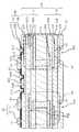
図9は、セル12Eの断面構成の一例を表す。図9には、セル12Eにおいて、発光素子15、駆動IC16、データ線Sigおよびクロック線CLKの形成されている箇所の断面構成の一例が示されている。(Structure of
FIG. 9 illustrates an example of a cross-sectional configuration of the
セル12Eは、例えば、配線基板30と、配線基板30の上面に接して形成された微細L/S層40と、微細L/S層40の上面に行列状に配置された複数の画素11とを有している。配線基板30は、配線基板12Dとの関係では中間基板としての役割を有している。 The
セル12Eは、さらに、例えば、各画素11を含む表面を被覆する埋め込み層44と、埋め込み層44に接して形成された遮光層45と、配線基板30の裏面に接して形成された絶縁層50とを有している。埋め込み層44は、可視光を透過する光透過性の材料で構成されている。遮光層45は、可視光を吸収する材料を含んで構成されている。絶縁層50は、例えば、紫外線硬化樹脂、または、熱硬化性樹脂で形成されている。 The
遮光層45は、各発光素子15と対向する箇所に開口45Aを有している。各発光素子15から発せられた光は各開口45Aを介して外部に出射される。絶縁層50は、セル12Eの外部接続端子としての各電極パッド34と対向する箇所に開口50Aを有している。従って、各電極パッド34は、開口50Aを介して、セル12E(配線基板30)の裏面に露出している。例えば、開口50A内に設けた金属バンプや半田バンプを介して、電極パッド34と配線基板12Dとが互いに電気的に接続されている。 The light shielding layer 45 has an opening 45 </ b> A at a location facing each light emitting
(配線基板30)
配線基板30は、ビア接合を利用した積層基板である。配線基板30は、配線基板30の裏面に、外部接続端子としての複数の電極パッド34を有している。複数の電極パッド34は、少なくともゲートドライバIC14Aごとに1つ以上設けられており、例えば、ゲートドライバIC14A、データ線Sig、電源線VDD1、参照電圧線Ref1、参照電圧線Ref2およびのこぎり電圧線Sawごとに、1つ以上設けられている。(Wiring board 30)
The
配線基板30は、微細L/S層40内で引き回された複数の配線17と、複数の電極パッド34とを電気的に接続する。配線基板30は、複数の配線17と、複数の電極パッド34とを電気的に接続する複数の貫通配線17を有している。各貫通配線17は、配線基板30を厚さ方向に貫通する配線である。ある貫通配線17は、配線基板30内で列方向に延在するデータ線Sigと、配線基板30内の一部の層を貫通する複数のビアとを含んでいる。ある貫通配線17は、配線基板30内で列方向に延在するクロック線CLKと、配線基板30内の一部の層を貫通する複数のビアとを含んでいる。 The
ある貫通配線17は、配線基板30内で列方向に延在する電源線VDD1と、配線基板30内の一部の層を貫通する複数のビアとを含んでいる。ある貫通配線17は、配線基板30内で列方向に延在する参照電圧線Ref1と、配線基板30内の一部の層を貫通する複数のビアとを含んでいる。ある貫通配線17は、配線基板30内で列方向に延在する参照電圧線Ref2と、配線基板30内の一部の層を貫通する複数のビアとを含んでいる。ある貫通配線17は、配線基板30内で列方向に延在するのこぎり電圧線Sawと、配線基板30内の一部の層を貫通する複数のビアとを含んでいる。 A certain through
ところで、上述したように、複数の画素11は、例えば、図5に示したように、行方向および列方向に等間隔で配置されている。このとき、画素11のピッチは、各セル12E内だけでなく、隣接する2つのセル12E間においても、等ピッチとなっていることが好ましい。各セル12Eでは、各セル12Eの外部接続端子としての複数の電極パッド34が、セル12Eの裏面に設けられている。そのため、実装面の上面の外縁に外部接続端子を設けたときのような、画素11配置に使用できない額縁領域を省略したり、最小限にしたりすることができる。従って、各セル12Eから、そのような額縁領域が省略されているか、または、各セル12Eにおける、そのような額縁領域が最小限となっている場合には、隣接する2つのセル12E間においても、画素11のピッチを等ピッチにすることができる。 By the way, as described above, the plurality of
配線基板30は、例えば、ビルドアップ基板であり、コア基板31と、コア基板31の上面に接して形成されたビルドアップ層32と、コア基板31の裏面に接して形成されたビルドアップ層33とを有している。 The
コア基板31は、セル12Eの剛性の確保するものであり、例えば、ガラスエポキシ基板である。ビルドアップ層32は、1層以上の配線層を有している。ビルドアップ層32は、例えば、図9に示したように、配線層32A、絶縁層32B、配線層32C、絶縁層32Dおよび配線層32Eを、コア基板31の上面側からこの順に有している。ビルドアップ層33は、1層以上の配線層を有している。ビルドアップ層33は、例えば、図9に示したように、配線層33A、絶縁層33B、配線層33C、絶縁層33Dおよび配線層33Eを、コア基板31の裏面側からこの順に有している。配線層32A,32C,32E,33A,33C,33Eは、例えば、銅で形成されている。絶縁層32B,32D,33B,33Dは、例えば、紫外線硬化樹脂、または、熱硬化性樹脂で形成されている。 The
各データ線Sigは、例えば、配線層32Cに形成されている。各ゲート線Gateは、データ線Sigとは異なる層に形成されており、例えば、配線基板30の上面の配線層である配線層32Eに形成されている。各クロック線CLKおよびシフト線SFTは、例えば、ゲート線Gateと同一の層内に形成されており、例えば、配線層32Eに形成されている。各電極パッド34は、ビルドアップ層33に形成されており、例えば、配線層33Eと同一の層内に形成されている。上述の中継配線は、例えば、配線層32Eに形成されている。 Each data line Sig is formed in the
(微細L/S層40)
微細L/S層40は、配線層42と、配線層42(各配線17)と配線基板30の上面との間に設けられた絶縁層41とを有している。絶縁層41は、配線層42(各配線17)と、配線基板30の上面とに接している。絶縁層41は、例えば、ゲート線Gateや、クロック線CLK、シフト線STFの上面と対向する位置に開口41Aを有している。開口41Aの底面には、例えば、ゲート線Gateや、クロック線CLK、シフト線STFの一部が露出している。絶縁層41は、例えば、VPAで形成されている。VPAは、レジストとして一般に使われるものであり、例えば、新日鉄化学社製のVPAが上市されている。絶縁層41がVPAで形成されている場合、例えば、VPAを選択的に露光・現像することによりVPAに開口41を形成することができる。(Fine L / S layer 40)
The fine L /
配線層42(各配線17)は、例えば、開口41Aの底面および側面を含む配線基板30の上面に接するシード層42Aと、シード層42Aの上面に接するめっき層42Bとを有している。シード層42Aは、製造過程においてめっき層42Bをめっきで形成する際のめっき成長面となる。シード層42Aは、開口41Aの底面と接しており、例えば、ゲート線Gateや、クロック線CLK、シフト線STFと電気的に接続されている。シード層42Aは、例えば、銅で形成されている。めっき層42Bは、製造過程においてシード層42Aをめっき成長面としてめっき処理により形成されたものである。なお、配線層42(各配線17)は、例えば、スパッタリングにより形成された層であってもよい。 The wiring layer 42 (each wiring 17) has, for example, a
上述したように、配線層42(各配線16)は、絶縁層41の上面に接して形成されている。一方、各画素11の電極は、シード層42Aの上面に接して形成されている。そのため、発光素子15および駆動IC16は、互いに同一の面(シード層42Aの上面)上に形成されているが、厳密には、配線層42(各配線16)の形成面(絶縁層41の上面)とは別の面に形成されている。しかし、各画素11の実装という観点からは、絶縁層41の上面とシード層42Aの上面とを含む面が実装面41Sとなっていると言える。従って、配線層42(各配線16)は、各画素11の実装面41Sに形成されており、かつ、各画素11と実質的に共通の面に形成されている。 As described above, the wiring layer 42 (each wiring 16) is formed in contact with the upper surface of the insulating
配線層42(各配線17)は、例えば、ゲートドライバIC14Aや、開口41A内に露出している部材(例えば、ゲート線Gate、クロック線CLK、シフト線STF)とめっき接合されている。配線層42(各配線17)をめっきにより形成する際に、配線層42(各配線17)と、ゲートドライバIC14Aや、開口41A内に露出している上記部材との接合が、配線層42(各配線17)の形成プロセスの中で一括して行われてもよい。配線層42(各配線17)は、例えば、画素11(発光素子15および駆動IC16)とめっき接合されている。配線層42(各配線17)をめっきにより形成する際に、配線層42(各配線17)と、画素11との接合が、配線層42(各配線17)の形成プロセスの中で一括して行われてもよい。 The wiring layer 42 (each wiring 17) is, for example, plated and bonded to the
微細L/S層40のL/S(line and space)は、配線基板30のL/Sよりも小さくなっている。L/Sとは、面内で最も狭い配線ピッチを指している。微細L/S層40のL/Sは、複数の信号線Sig、複数のゲート線Gate、複数の電圧線VDD1、複数の参照電圧線Ref1、複数の参照電圧線Ref2、およびのこぎり電圧線SawのL/Sよりも小さくなっている。微細L/S層40のL/Sは、例えば、25μm程度である。一方、配線基板30のL/Sは、例えば、75μm程度である。 The L / S (line and space) of the fine L /
[製造方法]
次に、図10〜図14を参照しつつ、セル12Eの製造方法の一例について説明する。図10〜図14は、セル12Eの製造過程の一例を工程順に表す。[Production method]
Next, an example of a method for manufacturing the
まず、配線基板30を用意する。次に、配線基板30の上面に絶縁層41を形成したのち、所定の方法で、絶縁層41に開口41Aを形成する(図10)。次に、開口41Aの底面および側面を含む配線基板30の上面にシード層42Aを形成する(図11)。 First, the
次に、表面全体に絶縁性の接着剤を塗布するなどして、発光素子15や、駆動IC16、ゲートドライバIC14A(以下、「発光素子15等」と称する。)を仮固定するための固定層43Aを形成する(図12参照)。接着剤の代わりに、シリコーン系やアクリル系で代表されるような粘着剤の層を固定層43Aとして形成してもよい。続いて、発光素子15等を固定層43Aによって仮固定する(図12)。このとき、発光素子15等の電極パッドを、後述のめっき処理において成長する金属体(めっき層42B)と接続可能となる程度に近づけて配置する。 Next, a fixing layer for temporarily fixing the
次に、発光素子15等を仮固定している部分(発光素子15等の底面に存在する部分)以外の固定層43Aを除去する。その結果、発光素子15等の底面だけに固定層43Aが残る(図13)。図13では、残った固定層43Aを固定層43と記載した。固定層43Aの除去に際して、例えば、ドライエッチングや有機溶剤浸漬等を行うことができる。なお、あらかじめ、発光素子15等を仮固定する場所にだけ、絶縁性の接着剤を塗布しておいてもよい。 Next, the
次に、シード層42Aをめっき成長面としてめっき処理を行い、シード層42Aの上面にめっき層42Bを形成する(図14)。これにより、配線層42(各配線17)が形成される。このとき、配線層42(各配線17)と、発光素子15等との接合が、配線層42(各配線17)の形成プロセスの中で一括して行われる。また、配線層42(各配線17)と、開口41A内に露出している上記部材との接合が、配線層42(各配線17)の形成プロセスの中で一括して行われる。その後は、発光素子15等を埋め込み層43で埋め込んだ後に、遮光層45を形成する(図9参照)。このようにして、セル12Eが製造される。 Next, a plating process is performed using the
[作用・効果]
次に、表示装置1の作用、効果について説明する。本実施の形態では、複数のゲートドライバIC14Aが、画素領域12aに配置されており、さらに、複数画素行ごとに、1つずつ割り当てられている。これにより、複数のゲートドライバIC14Aを、セル12Eの上面端部に設けたり、複数のゲートドライバIC14Aを実装したFPCの接続端子をセル12Eの上面端部に設けたりする必要がなくなる。その結果、複数のセル12Eや、複数のユニット基板12Cをタイリングしたときに表示映像の目地をより目立たなくすることができる。[Action / Effect]
Next, the operation and effect of the
<2.変形例>
[変形例1]
上記実施の形態では、一組のデータ線Sigが、1画素列ごとに1つずつ割り当てられていた。つまり、複数のデータ線Sigが、1画素列ごとに3つずつ割り当てられていた。しかし、駆動方式によっては、上記の一組のデータ線Sigを、単一のデータ線Sigに置き換えることもできる。<2. Modification>
[Modification 1]
In the above embodiment, one set of data lines Sig is assigned to each pixel column. That is, a plurality of data lines Sig are assigned three for each pixel column. However, depending on the driving method, the set of data lines Sig can be replaced with a single data line Sig.
[変形例2]
上記実施の形態では、複数のゲートドライバIC14Aは、複数画素行ごとに、1つずつ割り当てられていた。しかし、複数のゲートドライバIC14Aは、1画素行ごとに、1つずつ割り当てられていてもよい。[Modification 2]
In the above embodiment, a plurality of
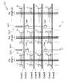
[変形例3]
また、上記実施の形態において、一組のデータ線Sigが、複数画素列ごとに1つずつ割り当てられていてもよい。つまり、複数のデータ線Sigが、複数画素列ごとに複数ずつ割り当てられていてもよい。例えば、図15に示したように、一組のデータ線Sigが、2画素列ごとに1つずつ割り当てられていてもよい。つまり、複数のデータ線Sigが、2画素列ごとに3ずつ割り当てられていてもよい。なお、本変形例においても、駆動方式によっては、上記の一組のデータ線Sigを、単一のデータ線Sigに置き換えることもできる。この場合、複数のデータ線Sigが、複数画素列ごとに1つずつ割り当てられている。[Modification 3]
In the above embodiment, one set of data lines Sig may be assigned to each of the plurality of pixel columns. That is, a plurality of data lines Sig may be assigned to each of a plurality of pixel columns. For example, as shown in FIG. 15, one set of data lines Sig may be assigned to every two pixel columns. That is, a plurality of data lines Sig may be assigned 3 for every 2 pixel columns. In this modification, the set of data lines Sig can be replaced with a single data line Sig depending on the driving method. In this case, a plurality of data lines Sig are assigned to each of the plurality of pixel columns.
このとき、複数のゲート線Gateは、1画素行において、1または複数のデータ線Sigを共用する画素数と等しい数の画素行をグループとしたときに、グループごとに、1画素行においてデータ線Sigを共用する画素数の2乗と等しい数ずつ割り当てられる。例えば、図15に示したように、複数のゲート線Gateは、2画素行をグループとしたときに、グループごとに、2の2乗(4つ)ずつ割り当てられる。 At this time, when a plurality of gate lines Gate group a number of pixel rows equal to the number of pixels sharing one or more data lines Sig in one pixel row, the data lines in one pixel row for each group. A number equal to the square of the number of pixels sharing Sig is assigned. For example, as illustrated in FIG. 15, when a plurality of gate lines Gate are grouped, 2 squares (four) are assigned to each group.
上記グループごとに割り当てられた複数のゲート線Gateは、各画素行において共通のデータ線Sigが割り当てられた画素11ごとに1つずつ割り当てられる。例えば、図15に示したように、上記グループごとに割り当てられた2つのゲート線Gateは、奇数列の画素11に対して1つ割り当てられ、偶数列の画素11に対して1つ割り当てられる。 A plurality of gate lines Gate assigned to each group are assigned to each
複数のゲートドライバIC14Aは、上記グループに含まれる画素行の数と等しい数ずつ割り当てられている。例えば、図15に示したように、複数のゲートドライバIC14Aは、グループごとに2つずつ割り当てられている。 The plurality of
本変形例では、複数のゲートドライバIC14Aが、画素領域12aに配置されており、さらに、データ線Sigを1画素行に含まれる複数の画素11で共用した上で、上記グループごとに、上記グループに含まれる画素行の数と等しい数ずつ割り当てられている。これにより、上記実施の形態と同一の画素11ピッチとしたときに、上記実施の形態よりも画素領域12aにより大きな空き領域を設けることができる。そのため、例えば、上記実施の形態の画素11ピッチよりも狭い画素11ピッチにした場合であっても、各ゲートドライバIC14Aを画素領域12aに配置することができる。従って、画素11ピッチを狭ピッチ化しつつ、複数のセル12Eや、複数のユニット基板12Cをタイリングしたときに表示映像の目地をより目立たなくすることができる。 In this modification, a plurality of
[変形例4]
また、上記変形例3では、各ゲートドライバIC14Aには、2本のゲート線Gateが接続されていたが、各ゲートドライバIC14Aに3本以上のゲート線Gateが接続されていてもよい。例えば、図16に示したように、各ゲートドライバIC14Aに、4本のゲート線Gateが接続されていてもよい。この場合には、各ゲートドライバIC14Aは、最後のゲート線Gateに対して選択信号を出力したときにだけ、選択信号の出力タイミングに同期してシフト信号を後段のゲートドライバIC14Aに出力する。各ゲートドライバIC14Aは、最後のゲート線Gate以外のゲート線Gateに対して選択信号を出力したときには、引き続き、次のゲート線Gateに対して選択信号を出力する。従って、このときは、各ゲートドライバIC14Aは、シフト信号を出力しない。[Modification 4]
In the third modification, two gate lines Gate are connected to each
各ゲートドライバIC14Aに3本以上のゲート線Gateが接続可能となった結果、複数のゲートドライバIC14Aを、上記グループごとに1つずつ割り当てることが可能である。例えば、各ゲートドライバIC14Aが、上記グループに含まれる画素行の数と等しい数のゲート線Gateに接続可能となっている場合、複数のゲートドライバIC14Aは、上記グループごとに1つずつ割り当てられる。例えば、図16に示したように、各ゲートドライバIC14Aが4本のゲート線Gateに接続可能となっている場合には、複数のゲート線Gateを4本のゲート線Gateごとにグループに分け、グループごとに1つずつゲートドライバIC14Aを割り当てることができる。 As a result of the fact that three or more gate lines Gate can be connected to each
本変形例においても、上記変形例3と同様、画素11ピッチを狭ピッチ化しつつ、複数のセル12Eや、複数のユニット基板12Cをタイリングしたときに表示映像の目地をより目立たなくすることができる。 Also in the present modification, as in the third modification, the pitch of the
[変形例5]
上記実施の形態において、画素11が、発光素子15および駆動IC16を一体に形成したものであってもよい。[Modification 5]
In the above embodiment, the
[変形例6]
また、上記実施の形態および変形例1〜6において、発光素子15の発光色が単一であってもよい。この場合に、セル12Eが、例えば、開口45A内に、複数色のカラーフィルタを有していてもよい。[Modification 6]
Moreover, in the said embodiment and the modifications 1-6, the luminescent color of the
<3.第2の実施の形態>
図17は、本技術の第2の実施の形態に係る照明装置2の概略構成の一例を表す。照明装置2は、上記第1の実施の形態およびその変形例(変形例1〜6)に係る表示装置1において、データ線Sigに入力される信号が、映像信号のような時々刻々、変化するものではなく、照明光の明るさに応じた固定値となっているものに相当する。照明装置2は、例えば、図17に示したように、照明パネルモジュール60と、照明パネルモジュール60を制御するコントローラ70とを備えている。照明パネルモジュール60は、例えば、照明パネル62と、照明パネル62の周囲に設けられた回路(ソースドライバ13、ゲートドライバ14)とを有している。<3. Second Embodiment>
FIG. 17 illustrates an example of a schematic configuration of the
(照明パネル62)
照明パネル62は、複数の画素61が照明パネル62の画素領域全面に渡って行列状に配置されたものである。画素領域は、照明パネル62において照明光が出射される領域(光出射領域)に相当する。照明パネル62は、コントローラ70によって各画素61がアクティブマトリクス駆動されることにより、照明光の明るさに応じた固定値である信号Vsigに基づく照明光を照明パネル62から出射する。照明パネル62は、行方向に延在する複数のゲート線Gateと、列方向に延在する複数のデータ線Sigとを有している。データ線Sigとゲート線Gateとの交差部分に対応して画素61が設けられている。(Lighting panel 62)
The
図18は、照明パネル62の斜視構成の一例を表す。照明パネル62は、実装基板62Aと、対向基板62Bとを互いに重ね合わせたものである。対向基板62Bの表面が光出射面となっている。対向基板62Bは、例えば、所定の間隙を介して、実装基板62Aと対向する位置に配置されている。なお、対向基板62Bが、実装基板62Aの上面に接していてもよい。対向基板62Bは、例えば、可視光を透過する光透過性の基板を有しており、例えば、ガラス基板、透明樹脂基板、または透明樹脂フィルムなどを有している。 FIG. 18 illustrates an example of a perspective configuration of the
実装基板62Aは、例えば、図2と同様に、タイル状に配置された複数のユニット基板で構成されている。ユニット基板は、例えば、タイル状に配置された複数のセルと、各セルを支持する支持基板とを有している。各ユニット基板は、さらに、制御基板(図示せず)を有し、各電極パッド34を介して、各セルと電気的に接続されている。上記の支持基板は、例えば、金属フレーム、もしくは、配線基板などで構成されている。上記の支持基板が配線基板で構成されている場合には、制御基板を兼ねることも可能である。各セルでは、例えば、図5、図6、図9、図15、図16において、データ線Sigに入力される信号が、固定値となっている場合に、画素61の駆動にとって必要のない配線が、適宜、省略される。 For example, the mounting
[作用・効果]
次に、照明装置2の作用、効果について説明する。本実施の形態では、上記第1の実施の形態およびその変形例に係る表示装置1と同様に、複数のゲートドライバIC14Aが、画素領域(光出射領域)に配置されており、さらに、所定のルールで割り当てられている。これにより、複数のゲートドライバIC14Aを、実装基板の上面端部に設けたり、複数のゲートドライバIC14Aを実装したFPCの接続端子を実装基板の上面端部に設けたりする必要がなくなる。その結果、複数の実装基板をタイリングしたときに照明光の目地をより目立たなくすることができる。[Action / Effect]
Next, functions and effects of the
<4.第3の実施の形態>
図19は、本技術の第3の実施の形態に係る受光装置3の概略構成の一例を表す。受光装置3は、上記第1の実施の形態およびその変形例(変形例1〜4)に係る表示装置1において、データ線Sigに入力される信号が、映像信号のような時々刻々、変化するものではなく、固定値となっているものに相当する。さらに、受光装置3は、上記第1の実施の形態およびその変形例(変形例1〜4)に係る表示装置1において、画素11の代わりに受光素子を設けたものに相当する。<4. Third Embodiment>
FIG. 19 illustrates an example of a schematic configuration of the
受光装置3は、例えば、図19に示したように、受光パネルモジュール80と、受光パネルモジュール80を制御するコントローラ90とを備えている。受光パネルモジュール80は、例えば、受光パネル82と、受光パネル82の周囲に設けられた回路(読み出し回路83、ゲートドライバ14)とを有している。 For example, as illustrated in FIG. 19, the
(受光パネル82)
受光パネル82は、複数の画素81が受光パネル82の画素領域全面に渡って行列状に配置されたものである。画素領域は、受光パネル82において外光が入射する領域(光入射領域)に相当する。受光パネル82は、コントローラ90によって各画素81がアクティブマトリクス駆動されることにより、固定の信号Vsigが読み出し回路83から入力された状態で、外光入射に基づく信号変化を読み出し回路83で検出する。受光パネル82は、行方向に延在する複数のゲート線Gateと、列方向に延在する複数のデータ線Sigとを有している。データ線Sigとゲート線Gateとの交差部分に対応して画素81が設けられている。(Light receiving panel 82)
The
図20は、受光パネル82の斜視構成の一例を表す。受光パネル82は、実装基板82Aと、対向基板82Bとを互いに重ね合わせたものである。対向基板82Bの表面が光入射面となっている。対向基板82Bは、例えば、所定の間隙を介して、実装基板82Aと対向する位置に配置されている。なお、対向基板82Bが、実装基板82Aの上面に接していてもよい。対向基板82Bは、例えば、可視光を透過する光透過性の基板を有しており、例えば、ガラス基板、透明樹脂基板、または透明樹脂フィルムなどを有している。 FIG. 20 illustrates an example of a perspective configuration of the
実装基板82Aは、例えば、図2と同様に、タイル状に配置された複数のユニット基板で構成されている。ユニット基板は、例えば、タイル状に配置された複数のセルと、各セルを支持する支持基板とを有している。各ユニット基板は、さらに、制御基板(図示せず)を有し、各電極パッド34を介して、各セルと電気的に接続されている。上記の支持基板は、例えば、金属フレーム、もしくは、配線基板などで構成されている。上記の支持基板が配線基板で構成されている場合には、制御基板を兼ねることも可能である。各セルでは、例えば、図5、図6、図9、図15、図16において、データ線Sigに入力される信号が、固定値となっている場合に、画素81の駆動にとって必要のない配線が、適宜、省略される。 For example, the mounting
[作用・効果]
次に、受光装置3の作用、効果について説明する。本実施の形態では、上記第1の実施の形態およびその変形例に係る表示装置1と同様に、複数のゲートドライバIC14Aが、画素領域(光入射領域)に配置されており、さらに、所定のルールで割り当てられている。これにより、複数のゲートドライバIC14Aを、実装基板の上面端部に設けたり、複数のゲートドライバIC14Aを実装したFPCの接続端子を実装基板の上面端部に設けたりする必要がなくなる。その結果、複数の実装基板をタイリングしたときに受光映像の目地をより目立たなくすることができる。[Action / Effect]
Next, functions and effects of the
<5.各実施の形態に共通の変形例>
上記各実施の形態およびその変形例において、遮光層45が対向基板12B,62B,82Bの裏面(実装基板12A,62A,82A側の表面)に配置されていてもよい。<5. Modification common to each embodiment>
In each of the above embodiments and modifications thereof, the light shielding layer 45 may be disposed on the back surface of the counter substrate 12B, 62B, 82B (the surface on the mounting
上記各実施の形態およびその変形例において、例えば、図21〜図23に示したように、対向基板12B,62B,82Bが省略されていてもよい。また、上記各実施の形態およびその変形例において、対向基板12B,62B,82Bが、ユニット基板12Cごとに、またはセル12Eごとに1つずつ設けられていてもよい。 In each of the above-described embodiments and modifications thereof, for example, as illustrated in FIGS. 21 to 23, the counter substrates 12B, 62B, and 82B may be omitted. In each of the above-described embodiments and modifications thereof, one counter substrate 12B, 62B, and 82B may be provided for each
上記各実施の形態およびその変形例において、遮光層45が省略されていてもよい。 In each of the above embodiments and modifications thereof, the light shielding layer 45 may be omitted.
また、上記各実施の形態およびその変形例では、各画素11,61,81は、配線層42(各配線17)とめっき接合されていた。しかし、各画素11,61,81は、例えば、配線層42(各配線17)と半田接合されていてもよい。例えば、各画素11,61,81の電極パッドに半田バンプを設けた上で、各画素11,61,81を、各配線17上に配置したのち、リフローを行う。これにより、各画素11,61,81を、各配線17に半田接合することができる。なお、本明細書中に記載された効果はあくまで例示であって限定されるものではなく、また、他の効果があってもよい。 In each of the above-described embodiments and modifications thereof, each
また、例えば、本技術は以下のような構成を取ることができる。
(1)
配線基板と、
前記配線基板の画素領域に行列状に配置された複数の画素と、
前記画素領域に配置され、複数の前記画素を複数個ずつ選択する複数の駆動部と
を備え、
各前記画素は、発光もしくは受光する光素子と、前記光素子の発光もしくは受光を制御する画素回路とを含み、
複数の前記駆動部は、1画素行ごと、もしくは複数画素行ごとに、1つずつ、もしくは複数ずつ割り当てられている
実装基板。
(2)
前記配線基板は、行方向に延在する複数の選択線と、列方向に延在する複数の信号線とを有し、
各前記画素回路は、前記選択線を介して入力される選択信号に基づいて、前記信号線を介して入力されるデータ信号のサンプリングを行い、
各前記駆動部は、シフト信号およびクロック信号に基づいて前記選択信号を前記選択線に出力することにより、前記データ信号が前記画素回路においてサンプリングされるタイミングを制御すると共に、前記選択信号の出力タイミングに同期して前記シフト信号を後段の前記駆動部に出力する
(1)に記載の実装基板。
(3)
前記配線基板は、前記駆動部ごとに1つ以上設けられ、前記駆動部と電気的に接続されると共に、前記配線基板の裏面に露出する複数の電極パッドを有し、
前記クロック信号は、少なくとも1つの前記電極パッドを介して外部から入力される
(1)または(2)に記載の実装基板。
(4)
複数の前記信号線は、1画素列ごとに1つずつ、もしくは複数ずつ割り当てられ、
複数の前記選択線は、1画素行ごとに1つずつ割り当てられ、
複数の前記駆動部は、1画素行ごとに1つずつ割り当てられている
(1)ないし(3)のいずれか1つに記載の実装基板。
(5)
複数の前記信号線は、複数画素列ごとに割り当てられ、
複数の前記選択線は、1画素行において前記信号線を共用する画素数と等しい数の画素行をグループとしたときに、前記グループごとに、1画素行において前記信号線を共用する画素数の2乗と等しい数ずつ割り当てられ、
前記グループごとに割り当てられた複数の前記選択線は、各画素行において共通の前記信号線が割り当てられた前記画素ごとに1つずつ割り当てられ、
複数の前記駆動部は、前記グループごとに1つずつ、もしくは前記グループに含まれる画素行の数と等しい数ずつ割り当てられている
(1)ないし(3)のいずれか1つに記載の実装基板。
(6)
複数の実装基板と、
複数の前記実装基板を制御する制御回路と
を備え、
前記実装基板は、
配線基板と、
前記配線基板の画素領域に行列状に配置された複数の画素と、
前記画素領域に配置され、複数の前記画素を複数個ずつ選択する複数の駆動部と
を有し、
各前記画素は、発光もしくは受光する光素子と、前記光素子の発光もしくは受光を制御する画素回路とを含み、
複数の前記駆動部は、1画素行ごと、もしくは複数画素行ごとに、1つずつ、もしくは複数ずつ割り当てられている
電子機器。
(7)
当該電子機器は、
複数の前記実装基板を支持する支持基板と、
複数の前記実装基板を制御する制御基板と
をさらに備え、
複数の前記実装基板は、前記支持基板上にタイル状に配置され、
各前記配線基板は、前記駆動部ごとに1つ以上設けられ、前記駆動部と電気的に接続されると共に、前記配線基板の裏面に露出する複数の電極パッドを有し、
前記支持基板および前記制御基板の少なくとも一方は、各前記電極パッドを介して、各前記配線基板と電気的に接続されている
(6)に記載の電子機器。For example, this technique can take the following composition.
(1)
A wiring board;
A plurality of pixels arranged in a matrix in a pixel region of the wiring board;
A plurality of driving units arranged in the pixel region and selecting a plurality of the plurality of pixels one by one,
Each of the pixels includes an optical element that emits or receives light, and a pixel circuit that controls light emission or reception of the optical element,
The plurality of driving units are assigned to each pixel row, or to each pixel row, one or more mounting boards.
(2)
The wiring board has a plurality of selection lines extending in a row direction and a plurality of signal lines extending in a column direction,
Each of the pixel circuits performs sampling of a data signal input through the signal line based on a selection signal input through the selection line,
Each of the drive units controls the timing at which the data signal is sampled in the pixel circuit by outputting the selection signal to the selection line based on a shift signal and a clock signal, and the output timing of the selection signal The mounting substrate according to (1), wherein the shift signal is output to the driving unit at a subsequent stage in synchronization with the driving signal.
(3)
One or more wiring boards are provided for each driving unit, and are electrically connected to the driving unit and have a plurality of electrode pads exposed on the back surface of the wiring board,
The mounting board according to (1) or (2), wherein the clock signal is input from the outside through at least one of the electrode pads.
(4)
The plurality of signal lines are assigned one by one or a plurality for each pixel column,
A plurality of the selection lines are assigned to each pixel row,
The mounting substrate according to any one of (1) to (3), wherein the plurality of driving units are assigned to each pixel row.
(5)
The plurality of signal lines are assigned to each of a plurality of pixel columns,
When the number of pixel lines equal to the number of pixels sharing the signal line in one pixel row is grouped, the plurality of the selection lines have the number of pixels sharing the signal line in one pixel row for each group. Assigned a number equal to the square,
The plurality of selection lines allocated for each group are allocated one by one for each pixel to which the common signal line is allocated in each pixel row,
The mounting substrate according to any one of (1) to (3), wherein the plurality of driving units are assigned one for each group or a number equal to the number of pixel rows included in the group. .
(6)
Multiple mounting boards;
A control circuit for controlling a plurality of the mounting boards,
The mounting substrate is
A wiring board;
A plurality of pixels arranged in a matrix in a pixel region of the wiring board;
A plurality of driving units arranged in the pixel region and selecting a plurality of the plurality of pixels one by one,
Each of the pixels includes an optical element that emits or receives light, and a pixel circuit that controls light emission or reception of the optical element,
The plurality of driving units are assigned to one pixel row or one pixel row or a plurality of pixel rows.
(7)
The electronic device
A support substrate for supporting a plurality of the mounting substrates;
A control board for controlling a plurality of the mounting boards,
The plurality of mounting substrates are arranged in a tile shape on the support substrate,
Each of the wiring boards is provided with one or more for each driving unit, and is electrically connected to the driving unit and has a plurality of electrode pads exposed on the back surface of the wiring board,
The electronic device according to (6), wherein at least one of the support substrate and the control substrate is electrically connected to each wiring substrate via each electrode pad.
1…表示装置、10…表示パネルモジュール、11…画素、12…表示パネル、12a…画素領域、12A…実装基板、12B…対向基板、12C…ユニット基板、12D…支持基板、12E…セル、13…ソースドライバ、14…ゲートドライバ、14A…ゲートドライバIC、15,15B,15G,15R…発光素子、15a,15b,15c,15d,15e,15f,16a,16b,16c,16d,16e,16f,16g,16h,16i,16k,16m,16n,16o,16p…電極パッド、15i…保護体、16…駆動IC、17…配線、18…貫通配線、20…コントローラ、30…配線基板、31…コア基板、32,33…ビルドアップ基板、32A,32C,32E,33A,33C,33E…配線層、32B,32D,33B,33D…絶縁層、34…電極パッド、40…微細L/S層、41…絶縁層、41A…開口、41S…実装面、42…配線層、42A…シード層、42B…めっき層、43,43A…固定層、44…埋め込み層、45…遮光層、45A…開口、50…絶縁層、50A…開口、60…照明パネルモジュール、61…画素、62…照明パネル、62A…実装基板、62B…対向基板、70…コントローラ、80…受光パネルモジュール、81…画素、82…受光パネル、82A…実装基板、82B…対向基板、90…コントローラ、CLK…クロック線、Gate,Gate1〜Gate8…ゲート線、GND…グラウンド線、Ref1,Ref2…参照電圧線、Saw…のこぎり電圧線、SFT…シフト線、Sig,SigB,SigB1,SigB2,SigG,SigG1,SigG2,SigR,SigR1,SigR2…データ線、VDD1,VDD2…電源線。 DESCRIPTION OF
Claims (7)
Translated fromJapanese前記配線基板の画素領域に行列状に配置された複数の画素と、
前記画素領域に配置され、複数の前記画素を複数個ずつ選択する複数の駆動部と
を備え、
各前記画素は、発光もしくは受光する光素子と、前記光素子の発光もしくは受光を制御する画素回路とを含み、
複数の前記駆動部は、1画素行ごと、もしくは複数画素行ごとに、1つずつ、もしくは複数ずつ割り当てられている
実装基板。A wiring board;
A plurality of pixels arranged in a matrix in a pixel region of the wiring board;
A plurality of driving units arranged in the pixel region and selecting a plurality of the plurality of pixels one by one,
Each of the pixels includes an optical element that emits or receives light, and a pixel circuit that controls light emission or reception of the optical element,
The plurality of driving units are assigned to each pixel row, or to each pixel row, one or more mounting boards.
各前記画素回路は、前記選択線を介して入力される選択信号に基づいて、前記信号線を介して入力されるデータ信号のサンプリングを行い、
各前記駆動部は、シフト信号およびクロック信号に基づいて前記選択信号を前記選択線に出力することにより、前記データ信号が前記画素回路においてサンプリングされるタイミングを制御すると共に、前記選択信号の出力タイミングに同期して前記シフト信号を後段の前記駆動部に出力する
請求項1に記載の実装基板。The wiring board has a plurality of selection lines extending in a row direction and a plurality of signal lines extending in a column direction,
Each of the pixel circuits performs sampling of a data signal input through the signal line based on a selection signal input through the selection line,
Each of the drive units controls the timing at which the data signal is sampled in the pixel circuit by outputting the selection signal to the selection line based on a shift signal and a clock signal, and the output timing of the selection signal The mounting board according to claim 1, wherein the shift signal is output to the driving unit at a subsequent stage in synchronization with the driving signal.
前記クロック信号は、少なくとも1つの前記電極パッドを介して外部から入力される
請求項2に記載の実装基板。One or more wiring boards are provided for each driving unit, and are electrically connected to the driving unit and have a plurality of electrode pads exposed on the back surface of the wiring board,
The mounting board according to claim 2, wherein the clock signal is input from the outside through at least one of the electrode pads.
複数の前記選択線は、1画素行ごとに1つずつ割り当てられ、
複数の前記駆動部は、1画素行ごとに1つずつ割り当てられている
請求項3に記載の実装基板。The plurality of signal lines are assigned one by one or a plurality for each pixel column,
A plurality of the selection lines are assigned to each pixel row,
The mounting board according to claim 3, wherein the plurality of driving units are assigned one by one for each pixel row.
複数の前記選択線は、1画素行において前記信号線を共用する画素数と等しい数の画素行をグループとしたときに、前記グループごとに、1画素行において前記信号線を共用する画素数の2乗と等しい数ずつ割り当てられ、
前記グループごとに割り当てられた複数の前記選択線は、各画素行において共通の前記信号線が割り当てられた前記画素ごとに1つずつ割り当てられ、
複数の前記駆動部は、前記グループごとに1つずつ、もしくは前記グループに含まれる画素行の数と等しい数ずつ割り当てられている
請求項3に記載の実装基板。The plurality of signal lines are assigned to each of a plurality of pixel columns,
When the number of pixel lines equal to the number of pixels sharing the signal line in one pixel row is grouped, the plurality of the selection lines have the number of pixels sharing the signal line in one pixel row for each group. Assigned a number equal to the square,
The plurality of selection lines allocated for each group are allocated one by one for each pixel to which the common signal line is allocated in each pixel row,
The mounting substrate according to claim 3, wherein the plurality of driving units are assigned one by one for each group or a number equal to the number of pixel rows included in the group.
複数の前記実装基板を制御する制御回路と
を備え、
前記実装基板は、
配線基板と、
前記配線基板の画素領域に行列状に配置された複数の画素と、
前記画素領域に配置され、複数の前記画素を複数個ずつ選択する複数の駆動部と
を有し、
各前記画素は、発光もしくは受光する光素子と、前記光素子の発光もしくは受光を制御する画素回路とを含み、
複数の前記駆動部は、1画素行ごと、もしくは複数画素行ごとに、1つずつ、もしくは複数ずつ割り当てられている
電子機器。Multiple mounting boards;
A control circuit for controlling a plurality of the mounting boards,
The mounting substrate is
A wiring board;
A plurality of pixels arranged in a matrix in a pixel region of the wiring board;
A plurality of driving units arranged in the pixel region and selecting a plurality of the plurality of pixels one by one,
Each of the pixels includes an optical element that emits or receives light, and a pixel circuit that controls light emission or reception of the optical element,
The plurality of driving units are assigned to one pixel row or one pixel row or a plurality of pixel rows.
複数の前記実装基板を支持する支持基板と、
複数の前記実装基板を制御する制御基板と
をさらに備え、
複数の前記実装基板は、前記支持基板上にタイル状に配置され、
各前記配線基板は、前記駆動部ごとに1つ以上設けられ、前記駆動部と電気的に接続されると共に、前記配線基板の裏面に露出する複数の電極パッドを有し、
前記支持基板および前記制御基板の少なくとも一方は、各前記電極パッドを介して、各前記配線基板と電気的に接続されている
請求項6に記載の電子機器。The electronic device
A support substrate for supporting a plurality of the mounting substrates;
A control board for controlling a plurality of the mounting boards,
The plurality of mounting substrates are arranged in a tile shape on the support substrate,
Each of the wiring boards is provided with one or more for each driving unit, and is electrically connected to the driving unit and has a plurality of electrode pads exposed on the back surface of the wiring board,
The electronic device according to claim 6, wherein at least one of the support substrate and the control substrate is electrically connected to each wiring substrate via each electrode pad.
Priority Applications (6)
| Application Number | Priority Date | Filing Date | Title |
|---|---|---|---|
| JP2014074842AJP2015197543A (en) | 2014-03-31 | 2014-03-31 | Mounting board and electronic equipment |
| US15/128,438US10510286B2 (en) | 2014-03-31 | 2015-03-17 | Mounting substrate and electronic apparatus |
| EP15773269.4AEP3128510A4 (en) | 2014-03-31 | 2015-03-17 | Mounting substrate and electronic device |
| CN201580015723.1ACN106133819B (en) | 2014-03-31 | 2015-03-17 | Install the base board and electronics |
| PCT/JP2015/057849WO2015151798A1 (en) | 2014-03-31 | 2015-03-17 | Mounting substrate and electronic device |
| CN201910631374.6ACN110277050B (en) | 2014-03-31 | 2015-03-17 | Electronic device |
Applications Claiming Priority (1)
| Application Number | Priority Date | Filing Date | Title |
|---|---|---|---|
| JP2014074842AJP2015197543A (en) | 2014-03-31 | 2014-03-31 | Mounting board and electronic equipment |
Publications (1)
| Publication Number | Publication Date |
|---|---|
| JP2015197543Atrue JP2015197543A (en) | 2015-11-09 |
Family
ID=54240130
Family Applications (1)
| Application Number | Title | Priority Date | Filing Date |
|---|---|---|---|
| JP2014074842APendingJP2015197543A (en) | 2014-03-31 | 2014-03-31 | Mounting board and electronic equipment |
Country Status (5)
| Country | Link |
|---|---|
| US (1) | US10510286B2 (en) |
| EP (1) | EP3128510A4 (en) |
| JP (1) | JP2015197543A (en) |
| CN (2) | CN106133819B (en) |
| WO (1) | WO2015151798A1 (en) |
Cited By (6)
| Publication number | Priority date | Publication date | Assignee | Title |
|---|---|---|---|---|
| JP2018087927A (en)* | 2016-11-29 | 2018-06-07 | Its合同会社 | LED display device |
| WO2020004663A1 (en) | 2018-06-29 | 2020-01-02 | 京セラ株式会社 | Display device |
| KR20200060595A (en)* | 2018-11-21 | 2020-06-01 | 삼성디스플레이 주식회사 | Tiled display device |
| JPWO2019167966A1 (en)* | 2018-02-28 | 2020-06-18 | 京セラ株式会社 | Display device, glass substrate, and method for manufacturing glass substrate |
| JP2020535629A (en)* | 2018-08-20 | 2020-12-03 | エルジー・ケム・リミテッド | Embedded electrode substrate for transparent light emitting element display and its manufacturing method |
| JP2023511470A (en)* | 2019-11-29 | 2023-03-20 | 京東方科技集團股▲ふん▼有限公司 | ARRAY SUBSTRATE, DISPLAY PANEL, SPLICING DISPLAY PANEL, AND DISPLAY DRIVING METHOD |
Families Citing this family (16)
| Publication number | Priority date | Publication date | Assignee | Title |
|---|---|---|---|---|
| JP2015197544A (en) | 2014-03-31 | 2015-11-09 | ソニー株式会社 | Mounting board and electronic apparatus |
| JP6128046B2 (en) | 2014-03-31 | 2017-05-17 | ソニー株式会社 | Mounting board and electronic equipment |
| WO2018101159A1 (en)* | 2016-12-01 | 2018-06-07 | シャープ株式会社 | Connection wiring |
| JP6289718B1 (en)* | 2017-01-02 | 2018-03-07 | ルーメンス カンパニー リミテッド | LED display device |
| KR102416380B1 (en)* | 2017-12-29 | 2022-07-01 | 엘지디스플레이 주식회사 | Display apparatus |
| KR102555210B1 (en)* | 2017-12-29 | 2023-07-12 | 엘지디스플레이 주식회사 | Light emitting display device |
| US11263963B2 (en) | 2018-05-09 | 2022-03-01 | Apple Inc. | Local passive matrix display |
| KR102606922B1 (en) | 2018-07-06 | 2023-11-27 | 삼성디스플레이 주식회사 | Display device and Method of manufacturing the same |
| DE102019123893A1 (en)* | 2019-09-05 | 2021-03-11 | OSRAM Opto Semiconductors Gesellschaft mit beschränkter Haftung | DISPLAY MODULE, SCREEN AND METHOD OF OPERATING A DISPLAY MODULE |
| CN111402743A (en) | 2020-03-24 | 2020-07-10 | 昆山国显光电有限公司 | Display panel and display device |
| CN114365213B (en)* | 2020-06-18 | 2023-12-08 | 京东方科技集团股份有限公司 | Display panel, manufacturing method thereof and display device |
| US12046201B2 (en) | 2020-06-18 | 2024-07-23 | Boe Technology Group Co., Ltd. | Display panel and manufacturing method thereof, and display device |
| KR102813637B1 (en)* | 2021-03-02 | 2025-05-28 | 삼성디스플레이 주식회사 | Display device, method of manufacturing the same and tiled display device including the same |
| CN113257130B (en) | 2021-05-17 | 2022-07-12 | 武汉华星光电技术有限公司 | Display panel of display area integrated grid drive circuit |
| CN115631710B (en)* | 2021-07-16 | 2025-03-21 | 群创光电股份有限公司 | Display Panel |
| JP2024528762A (en)* | 2021-08-20 | 2024-08-01 | 京東方科技集團股▲ふん▼有限公司 | Display device, display panel, and driving method thereof |
Family Cites Families (52)
| Publication number | Priority date | Publication date | Assignee | Title |
|---|---|---|---|---|
| CA2241555C (en) | 1995-12-29 | 2006-07-11 | Cree Research, Inc. | True color flat panel display using an led dot matrix and led dot matrix drive method and apparatus |
| US5812105A (en) | 1996-06-10 | 1998-09-22 | Cree Research, Inc. | Led dot matrix drive method and apparatus |
| TW575196U (en)* | 1996-09-24 | 2004-02-01 | Toshiba Electronic Eng | Liquid crystal display device |
| JP3560756B2 (en)* | 1997-02-13 | 2004-09-02 | アルプス電気株式会社 | Driving method of display device |
| US6897855B1 (en) | 1998-02-17 | 2005-05-24 | Sarnoff Corporation | Tiled electronic display structure |
| TW491959B (en)* | 1998-05-07 | 2002-06-21 | Fron Tec Kk | Active matrix type liquid crystal display devices, and substrate for the same |
| JP2004500731A (en)* | 1998-06-18 | 2004-01-08 | ソニー エレクトロニクス インク | Method and apparatus for splitting, scaling and displaying video and / or graphic images across multiple display devices |
| JP2001215528A (en)* | 2000-02-03 | 2001-08-10 | Matsushita Electric Ind Co Ltd | LCD panel with built-in peripheral drive circuit |
| JP2001242435A (en)* | 2000-02-25 | 2001-09-07 | Hitachi Ltd | LCD multi-display device |
| JP4887587B2 (en) | 2001-08-01 | 2012-02-29 | ソニー株式会社 | Image display device and manufacturing method thereof |
| WO2003023745A1 (en)* | 2001-09-07 | 2003-03-20 | Matsushita Electric Industrial Co., Ltd. | Display apparatus and its manufacturing method |
| US7034470B2 (en)* | 2002-08-07 | 2006-04-25 | Eastman Kodak Company | Serially connecting OLED devices for area illumination |
| KR20040013957A (en)* | 2002-08-09 | 2004-02-14 | 엘지전자 주식회사 | multi-vision and picture visualizing method the same |
| JP2005033141A (en) | 2003-07-11 | 2005-02-03 | Sony Corp | Semiconductor device, its manufacturing method, false wafer, its manufacturing method, and packaging structure of semiconductor device |
| KR100570774B1 (en)* | 2004-08-20 | 2006-04-12 | 삼성에스디아이 주식회사 | Memory management method for display data of light emitting display device |
| KR101074402B1 (en)* | 2004-09-23 | 2011-10-17 | 엘지디스플레이 주식회사 | Liquid crystal display device and method for driving the same |
| US7812794B2 (en)* | 2004-12-06 | 2010-10-12 | Semiconductor Energy Laboratory Co., Ltd. | Display device and driving method thereof |
| JP2006251534A (en) | 2005-03-11 | 2006-09-21 | Sharp Corp | Display device |
| EP1770788A3 (en)* | 2005-09-29 | 2011-09-21 | Semiconductor Energy Laboratory Co., Ltd. | Semiconductor device having oxide semiconductor layer and manufacturing method thereof |
| KR101115026B1 (en) | 2006-01-10 | 2012-03-06 | 삼성전자주식회사 | Gate driver, thin film transistor substrate and liquid crystal display having the same |
| JP5336700B2 (en)* | 2006-11-30 | 2013-11-06 | ローム株式会社 | Semiconductor device and electronic apparatus using the same |
| US20080211760A1 (en)* | 2006-12-11 | 2008-09-04 | Seung-Soo Baek | Liquid Crystal Display and Gate Driving Circuit Thereof |
| GB0718656D0 (en)* | 2007-05-16 | 2007-11-07 | Seereal Technologies Sa | Holograms |
| JP4483905B2 (en) | 2007-08-03 | 2010-06-16 | ソニー株式会社 | Display device and wiring routing method |
| KR20090078577A (en) | 2008-01-15 | 2009-07-20 | 삼성에스디아이 주식회사 | Scan driver and flat panel display using the same |
| CN101978409B (en)* | 2008-01-21 | 2013-07-17 | 视瑞尔技术公司 | Device for controlling pixels and electronic display unit |
| KR101490789B1 (en)* | 2008-12-18 | 2015-02-06 | 삼성디스플레이 주식회사 | Liqiud crystal display |
| TW201027502A (en)* | 2009-01-15 | 2010-07-16 | Novatek Microelectronics Corp | Gate driver and display driver using thereof |
| US8279145B2 (en) | 2009-02-17 | 2012-10-02 | Global Oled Technology Llc | Chiplet driver pairs for two-dimensional display |
| JP2010238323A (en)* | 2009-03-31 | 2010-10-21 | Casio Computer Co Ltd | Shift register and electronic device |
| US8305294B2 (en)* | 2009-09-08 | 2012-11-06 | Global Oled Technology Llc | Tiled display with overlapping flexible substrates |
| KR101654834B1 (en)* | 2009-11-05 | 2016-09-07 | 삼성디스플레이 주식회사 | Thin film transistor display panel and method of manufacturing the same |
| JP5482393B2 (en)* | 2010-04-08 | 2014-05-07 | ソニー株式会社 | Display device, display device layout method, and electronic apparatus |
| JP2012042567A (en) | 2010-08-16 | 2012-03-01 | Funai Electric Co Ltd | Liquid crystal display and liquid crystal module |
| KR101741717B1 (en)* | 2010-10-15 | 2017-05-30 | 글로벌 오엘이디 테크놀러지 엘엘씨 | Chiplet Display with Multiple Passive-Matrix Controllers |
| JP2012142376A (en) | 2010-12-28 | 2012-07-26 | Sanyo Electric Co Ltd | Element mounting substrate, portable device, and method for manufacturing element mounting substrate |
| JP5966412B2 (en) | 2011-04-08 | 2016-08-10 | ソニー株式会社 | Pixel chip, display panel, lighting panel, display device and lighting device |
| US20120256957A1 (en)* | 2011-04-10 | 2012-10-11 | Sau-Kwo Chiu | Image processing method of performing scaling operations upon respective data portions for multi-channel transmission and image processing apparatus thereof |
| KR101850990B1 (en)* | 2011-07-06 | 2018-04-23 | 삼성디스플레이 주식회사 | Display device and driving method thereof |
| JP6176117B2 (en)* | 2012-01-10 | 2017-08-09 | 株式会社Joled | Display device and display method |
| JP5989420B2 (en) | 2012-06-28 | 2016-09-07 | 株式会社東芝 | Semiconductor light emitting device |
| KR101484681B1 (en)* | 2012-11-01 | 2015-01-20 | 엘지디스플레이 주식회사 | Organic light emitting display device |
| CN103021359B (en)* | 2012-12-10 | 2015-11-25 | 京东方科技集团股份有限公司 | A kind of array base palte and drived control method thereof and display device |
| US9153171B2 (en)* | 2012-12-17 | 2015-10-06 | LuxVue Technology Corporation | Smart pixel lighting and display microcontroller |
| GB2519587A (en)* | 2013-10-28 | 2015-04-29 | Barco Nv | Tiled Display and method for assembling same |
| KR102204976B1 (en)* | 2013-11-13 | 2021-01-20 | 삼성디스플레이 주식회사 | Display apparatus and fabrication method thereof |
| KR20150066901A (en)* | 2013-12-09 | 2015-06-17 | 삼성전자주식회사 | Driving apparatus and method of a display panel |
| US9367094B2 (en)* | 2013-12-17 | 2016-06-14 | Apple Inc. | Display module and system applications |
| US9490276B2 (en)* | 2014-02-25 | 2016-11-08 | Lg Display Co., Ltd. | Display backplane and method of fabricating the same |
| KR102119583B1 (en)* | 2014-03-31 | 2020-06-17 | 엘지디스플레이 주식회사 | Liquid crystal display device |
| JP6128046B2 (en) | 2014-03-31 | 2017-05-17 | ソニー株式会社 | Mounting board and electronic equipment |
| JP2015197544A (en) | 2014-03-31 | 2015-11-09 | ソニー株式会社 | Mounting board and electronic apparatus |
- 2014
- 2014-03-31JPJP2014074842Apatent/JP2015197543A/enactivePending
- 2015
- 2015-03-17CNCN201580015723.1Apatent/CN106133819B/enactiveActive
- 2015-03-17EPEP15773269.4Apatent/EP3128510A4/ennot_activeCeased
- 2015-03-17CNCN201910631374.6Apatent/CN110277050B/enactiveActive
- 2015-03-17USUS15/128,438patent/US10510286B2/enactiveActive
- 2015-03-17WOPCT/JP2015/057849patent/WO2015151798A1/enactiveApplication Filing
Cited By (13)
| Publication number | Priority date | Publication date | Assignee | Title |
|---|---|---|---|---|
| JP2018087927A (en)* | 2016-11-29 | 2018-06-07 | Its合同会社 | LED display device |
| JPWO2019167966A1 (en)* | 2018-02-28 | 2020-06-18 | 京セラ株式会社 | Display device, glass substrate, and method for manufacturing glass substrate |
| US11430377B2 (en) | 2018-06-29 | 2022-08-30 | Kyocera Corporation | Display device |
| KR20210019542A (en) | 2018-06-29 | 2021-02-22 | 교세라 가부시키가이샤 | Display device |
| WO2020004663A1 (en) | 2018-06-29 | 2020-01-02 | 京セラ株式会社 | Display device |
| US11769446B2 (en) | 2018-06-29 | 2023-09-26 | Kyocera Corporation | Display device |
| JP2020535629A (en)* | 2018-08-20 | 2020-12-03 | エルジー・ケム・リミテッド | Embedded electrode substrate for transparent light emitting element display and its manufacturing method |
| KR20200060595A (en)* | 2018-11-21 | 2020-06-01 | 삼성디스플레이 주식회사 | Tiled display device |
| KR102577240B1 (en)* | 2018-11-21 | 2023-09-12 | 삼성디스플레이 주식회사 | Tiled display device |
| JP2023511470A (en)* | 2019-11-29 | 2023-03-20 | 京東方科技集團股▲ふん▼有限公司 | ARRAY SUBSTRATE, DISPLAY PANEL, SPLICING DISPLAY PANEL, AND DISPLAY DRIVING METHOD |
| JP7422869B2 (en) | 2019-11-29 | 2024-01-26 | 京東方科技集團股▲ふん▼有限公司 | Array substrate, display panel, splicing display panel, and display driving method |
| JP2024056691A (en)* | 2019-11-29 | 2024-04-23 | 京東方科技集團股▲ふん▼有限公司 | ARRAY SUBSTRATE, DISPLAY PANEL, SPLICING DISPLAY PANEL, AND DISPLAY DRIVING METHOD |
| JP7676600B2 (en) | 2019-11-29 | 2025-05-14 | 京東方科技集團股▲ふん▼有限公司 | ARRAY SUBSTRATE, DISPLAY PANEL, SPLICING DISPLAY PANEL, AND DISPLAY DRIVING METHOD |
Also Published As
| Publication number | Publication date |
|---|---|
| EP3128510A4 (en) | 2017-12-06 |
| WO2015151798A1 (en) | 2015-10-08 |
| US20180218668A1 (en) | 2018-08-02 |
| EP3128510A1 (en) | 2017-02-08 |
| CN110277050B (en) | 2022-12-30 |
| CN110277050A (en) | 2019-09-24 |
| US10510286B2 (en) | 2019-12-17 |
| CN106133819B (en) | 2019-08-06 |
| CN106133819A (en) | 2016-11-16 |
Similar Documents
| Publication | Publication Date | Title |
|---|---|---|
| WO2015151798A1 (en) | Mounting substrate and electronic device | |
| JP6128046B2 (en) | Mounting board and electronic equipment | |
| US12027429B2 (en) | Mounting substrate and electronic apparatus | |
| CN107750377B (en) | Display panel redundancy scheme | |
| JP2011100716A (en) | Light source module and electronic equipment having the same | |
| JP2014039035A (en) | Led display panel and led display device | |
| CN113614823A (en) | Display device | |
| TW201909407A (en) | Transparent active matrix display comprising emitting pixels with colored light-emitting diodes | |
| KR20140050831A (en) | Chip on film package and organic light emitting display device having the same | |
| US20240290927A1 (en) | Light emitting module for a light emitting display | |
| KR20220068446A (en) | Display module, display apparatus and method for manufacturing the same | |
| CN114938677B (en) | Light-emitting substrate and display device | |
| JP6527194B2 (en) | Display device | |
| US10403197B2 (en) | Gate driver IC, chip-on-film substrate, and display apparatus | |
| KR20110030780A (en) | Drive ic and display device using thereof | |
| EP4622404A2 (en) | Systems and methods for configuring a display device and display system | |
| US11270633B1 (en) | Skewing drive times of LED zones in a display device with distributed driver circuits |