JP2015194448A - Phased array transmitter, transceiver and radar equipment - Google Patents
Phased array transmitter, transceiver and radar equipmentDownload PDFInfo
- Publication number
- JP2015194448A JP2015194448AJP2014073328AJP2014073328AJP2015194448AJP 2015194448 AJP2015194448 AJP 2015194448AJP 2014073328 AJP2014073328 AJP 2014073328AJP 2014073328 AJP2014073328 AJP 2014073328AJP 2015194448 AJP2015194448 AJP 2015194448A
- Authority
- JP
- Japan
- Prior art keywords
- transmission
- signal
- phased array
- pll
- self
- Prior art date
- Legal status (The legal status is an assumption and is not a legal conclusion. Google has not performed a legal analysis and makes no representation as to the accuracy of the status listed.)
- Granted
Links
Images


Classifications
- G—PHYSICS
- G01—MEASURING; TESTING
- G01S—RADIO DIRECTION-FINDING; RADIO NAVIGATION; DETERMINING DISTANCE OR VELOCITY BY USE OF RADIO WAVES; LOCATING OR PRESENCE-DETECTING BY USE OF THE REFLECTION OR RERADIATION OF RADIO WAVES; ANALOGOUS ARRANGEMENTS USING OTHER WAVES
- G01S7/00—Details of systems according to groups G01S13/00, G01S15/00, G01S17/00
- G01S7/02—Details of systems according to groups G01S13/00, G01S15/00, G01S17/00 of systems according to group G01S13/00
- G01S7/35—Details of non-pulse systems
- H—ELECTRICITY
- H01—ELECTRIC ELEMENTS
- H01Q—ANTENNAS, i.e. RADIO AERIALS
- H01Q1/00—Details of, or arrangements associated with, antennas
- H01Q1/27—Adaptation for use in or on movable bodies
- H01Q1/32—Adaptation for use in or on road or rail vehicles
- H01Q1/3208—Adaptation for use in or on road or rail vehicles characterised by the application wherein the antenna is used
- H01Q1/3233—Adaptation for use in or on road or rail vehicles characterised by the application wherein the antenna is used particular used as part of a sensor or in a security system, e.g. for automotive radar, navigation systems
- H—ELECTRICITY
- H01—ELECTRIC ELEMENTS
- H01Q—ANTENNAS, i.e. RADIO AERIALS
- H01Q3/00—Arrangements for changing or varying the orientation or the shape of the directional pattern of the waves radiated from an antenna or antenna system
- H01Q3/26—Arrangements for changing or varying the orientation or the shape of the directional pattern of the waves radiated from an antenna or antenna system varying the relative phase or relative amplitude of energisation between two or more active radiating elements; varying the distribution of energy across a radiating aperture
- H01Q3/267—Phased-array testing or checking devices
Landscapes
- Engineering & Computer Science (AREA)
- Radar, Positioning & Navigation (AREA)
- Remote Sensing (AREA)
- Computer Networks & Wireless Communication (AREA)
- Physics & Mathematics (AREA)
- General Physics & Mathematics (AREA)
- Computer Security & Cryptography (AREA)
- Radar Systems Or Details Thereof (AREA)
- Radio Transmission System (AREA)
Abstract
Translated fromJapaneseDescription
Translated fromJapaneseこの出願で言及する実施例は、フェーズドアレイ送信機,送受信機およびレーダー装置に関する。 The embodiments referred to in this application relate to phased array transmitters, transceivers and radar equipment.
従来、配列された複数のアンテナ(フェーズドアレイアンテナ)に対して、位相制御された送信信号をそれぞれ入力し、指向性を制御して送信波(放射電波)を出力するフェーズドアレイ送信機が知られている。このフェーズドアレイ送信機は、例えば、フェーズドアレイレーダーや大容量のデータ伝送を行う無線通信システムの送信機として使用される。 Conventionally, a phased array transmitter is known in which a phase-controlled transmission signal is input to each of a plurality of arranged antennas (phased array antennas), and directivity is controlled to output a transmission wave (radiated radio wave). ing. This phased array transmitter is used, for example, as a transmitter in a phased array radar or a wireless communication system that performs large-capacity data transmission.
近年、フェーズドアレイレーダーは、例えば、FM−CW(Frequency Modulated Continuous Wave)レーダーとしての適用が注目されている。このFM−CWレーダーは、比較的簡易な構成により対象物との距離および相対速度を高精度に測定可能なため、例えば、自動車に搭載して衝突を未然に回避し、或いは、前方車両との距離を一定に保持した自動走行を行うことが提案されている。 In recent years, phased array radar has attracted attention as an FM-CW (Frequency Modulated Continuous Wave) radar, for example. Since this FM-CW radar can measure the distance and relative speed with high accuracy with a relatively simple configuration, for example, it can be mounted on an automobile to avoid a collision in advance or It has been proposed to perform automatic driving while keeping the distance constant.
ところで、例えば、FM−CWレーダーに用いられるフェーズドアレイ送信機(送受信機)において、送信信号が正常であることを自己検査(自己診断)する自己検査(BIST:Built-In Self Test)回路が搭載されている。 By the way, for example, in a phased array transmitter (transmitter / receiver) used for FM-CW radar, a self-inspection (BIST: Built-In Self Test) circuit for self-inspection (self-diagnosis) of the transmission signal is installed. Has been.
ここで、BIST回路は、例えば、フェーズドアレイ送信機が形成された半導体チップの製造時やFM−CWレーダー装置の組み立て時における検査工程の削減、或いは、製品動作時における異常検出や動作補償(振幅・位相制御)を行うために利用される。 Here, for example, the BIST circuit reduces the number of inspection processes when manufacturing a semiconductor chip on which a phased array transmitter is formed or when assembling an FM-CW radar device, or detects abnormalities or compensates for operation (amplitude)・ Used to perform phase control.
製品動作時としては、例えば、フェーズドアレイ送信機が設けられたFM−CWレーダー装置の電源投入時、若しくは、FM−CWレーダー装置が使用される環境温度の急激な変化時等において、自己検査を行って放出電波の指向特性を制御する。 When the product is operating, for example, when the FM-CW radar device provided with the phased array transmitter is turned on, or when the environmental temperature at which the FM-CW radar device is used changes suddenly, self-inspection is performed. Control the directivity of the emitted radio wave.
ところで、従来、フェーズドアレイ送信機,送受信機或いはレーダー装置としては、様々なものが提案されている。 By the way, conventionally, various types of phased array transmitters, transceivers, and radar devices have been proposed.
前述したように、例えば、BIST回路が搭載されたFM−CWレーダー装置が提案されているが、例えば、送信用のPLL(Phase Locked Loop)とBIST用のPLLは、それぞれ専用のデジタル回路で制御されるようになっている。 As described above, for example, an FM-CW radar apparatus equipped with a BIST circuit has been proposed. For example, a transmission PLL (Phase Locked Loop) and a BIST PLL are controlled by dedicated digital circuits, respectively. It has come to be.
このように、送信用PLL(PLL-TX)と自己検査用PLL(BIST用PLL:PLL-BIST)に対してそれぞれ専用のデジタル回路を設けると、消費電力および占有面積の増大を招くことになる。さらに、PLL-TXおよびPLL-BISTの設定に時間が掛かるため、BIST回路を利用した処理に長時間を要することになってしまう。 As described above, when dedicated digital circuits are provided for the transmission PLL (PLL-TX) and the self-inspection PLL (BIST PLL: PLL-BIST), the power consumption and the occupied area are increased. . Furthermore, since it takes time to set PLL-TX and PLL-BIST, a long time is required for processing using the BIST circuit.
一実施形態によれば、基準送信信号を生成する送信用PLLと、前記送信用PLLを制御する制御回路と、送信ユニットと、遅延回路と、自己検査用PLLと、を有するフェーズドアレイ送信機が提供される。 According to one embodiment, a phased array transmitter having a transmission PLL that generates a reference transmission signal, a control circuit that controls the transmission PLL, a transmission unit, a delay circuit, and a self-test PLL. Provided.
前記送信ユニットは、前記基準送信信号を受け取り、それぞれ増幅および位相制御してユニット送信波を出力し、前記遅延回路は、前記基準送信信号に基づく信号を遅延し、前記自己検査用PLLは、前記遅延回路の出力信号を受け取り、自己検査を行う。 The transmission unit receives the reference transmission signal, outputs a unit transmission wave by performing amplification and phase control, respectively, the delay circuit delays a signal based on the reference transmission signal, and the self-inspection PLL Receives the output signal of the delay circuit and performs a self-test.
開示のフェーズドアレイ送信機,送受信機およびレーダー装置は、消費電力および占有面積を低減することができるという効果を奏する。 The disclosed phased array transmitter, transmitter / receiver, and radar apparatus have an effect of reducing power consumption and occupied area.
まず、フェーズドアレイ送信機,送受信機およびレーダー装置の実施例を詳述する前に、フェーズドアレイ送信機の例、並びに、その問題点を、図1〜図4を参照して説明する。 First, before describing embodiments of a phased array transmitter, a transceiver, and a radar device in detail, an example of a phased array transmitter and its problems will be described with reference to FIGS.
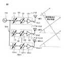
図1は、フェーズドアレイ送信機の動作を説明するための図である。図1において、参照符号110は基準送信信号生成器、101,102,…,10n+1は送信ユニット、そして、ANT1,ANT2,…,ANTn+1は送信アンテナを示す。 FIG. 1 is a diagram for explaining the operation of the phased array transmitter. In FIG. 1,
図1に示されるように、フェーズドアレイ送信機は、例えば、基準送信信号生成器110、n+1チャネルの送信ユニット101,102,…,10n+1、および、n+1チャネルの送信アンテナANT1,ANT2,…,ANTn+1を有する。 As shown in FIG. 1, the phased array transmitter includes, for example, a reference
送信ユニット101,102,…,10n+1は、可変利得アンプ111,112,…,11n+1、移相器121,122,…,12n+1、および、パワーアンプ131,132,…,13n+1を含む。可変利得アンプ111,112,…,11n+1は、基準送信信号生成器110で生成された基準送信信号Sotxを受け取り、基準送信信号Sotxの振幅を可変増幅して、移相器121,122,…,12n+1に出力する。 The
移相器121,122,…,12n+1は、可変利得アンプ111,112,…,11n+1からの出力信号をそれぞれ所定の位相だけシフトさせ、パワーアンプ131,132,…,13n+1に出力する。パワーアンプ131,132,…,13n+1は、移相器121,122,…,12n+1からの出力信号を電力増幅し、その出力信号(電波)Stx1,Stx2,…,Stxn+1を、送信アンテナANT1,ANT2,…,ANTn+1を介して放射する。 The
例えば、フェーズドアレイ送信機は、各送信アンテナANT1,ANT2,…,ANTn+1から放射される電波の位相を、電気的に制御して光路差の分だけずらし、電波の放射方向に垂直な面で位相を揃えるようになっている。 For example, the phased array transmitter is a plane perpendicular to the radiation direction of the radio wave by electrically controlling the phase of the radio wave radiated from each of the transmission antennas ANT1, ANT2,. It is designed to align the phase.
ここで、第1チャネルの送信ユニット101は、送信アンテナANT1を介して位相φの電波Stx1を放射し、第2チャネルの送信ユニット102は、送信アンテナANT2を介して位相φ+Δφの電波Stx2を放射する。 Here, the
さらに、第3チャネルの送信ユニット103(図示しない)は、送信アンテナANT3を介して位相φ+2Δφの電波Stx3を放射し、そして、第n+1チャネルの送信ユニット10n+1は、送信アンテナANTn+1を介して位相φ+nΔφの電波Stxn+1を放射する。 Further, the third channel transmission unit 103 (not shown) radiates the radio wave Stx3 having the phase φ + 2Δφ via the transmission antenna ANT3, and the (n + 1) th
以上により、各送信アンテナANT1,ANT2,…,ANTn+1からは、それぞれ所定の位相差(φ,φ+Δφ,…,φ+nΔφ)を有する電波(Stx1,Stx2,…,Stxn+1)が放射され、その放射電波の等位相面を制御することができるようになっている。なお、各送信ユニット101,102,…,10n+1は、位相の調整と共に、振幅の調整も行う。 As described above, radio waves (Stx1, Stx2,..., Stxn + 1) having predetermined phase differences (φ, φ + Δφ,..., Φ + nΔφ) are radiated from the transmission antennas ANT1, ANT2,. The equiphase surface of the radiated radio wave can be controlled. Each
このようなフェーズドアレイ送信機は、例えば、自動車に搭載するフェーズドアレイレーダー、或いは、大容量のデータ通信を行う無線通信システム等に適用される。なお、フェーズドアレイ送信機には、例えば、ミリ波帯域の周波数(30GHz〜300GHz)を利用することができるが、これに限定されず、より波長の短いテラヘルツの周波数を利用してもよい。 Such a phased array transmitter is applied to, for example, a phased array radar mounted on an automobile or a wireless communication system that performs large-capacity data communication. For the phased array transmitter, for example, a millimeter-wave band frequency (30 GHz to 300 GHz) can be used, but the present invention is not limited to this, and a terahertz frequency having a shorter wavelength may be used.
図2は、フェーズドアレイ送信機の一例を示すブロック図であり、BIST回路を搭載したフェーズドアレイ送信機、例えば、FM−CWレーダー装置におけるフェーズドアレイ送信機(送受信機)の一例を示すものである。 FIG. 2 is a block diagram showing an example of a phased array transmitter, and shows an example of a phased array transmitter equipped with a BIST circuit, for example, a phased array transmitter (transceiver) in an FM-CW radar apparatus. .
なお、図2では、説明を簡略化するために2つの送信ユニット101,102、送信アンテナANT1,ANT2およびスイッチSW1,SW2だけが描かれているが、例えば、上述した図1と同様に、実際には、n+1個の送信ユニット101,102,…,10n+1等が設けられている。 In FIG. 2, only two
図2に示されるように、フェーズドアレイ送信機は、2つ(複数)の送信ユニット101,102、2つの送信アンテナANT1,ANT2、2つのスイッチSW1,SW2、送信用PLL(PLL-TX)20およびBIST用PLL(自己検査用PLL:PLL-BIST)40を含む。 As shown in FIG. 2, the phased array transmitter includes two (a plurality of)
さらに、フェーズドアレイ送信機は、送信用デジタル制御回路30、BIST用デジタル制御回路50、ミキサ(混合器)6およびアナログ振幅・位相検出回路70を含む。ここで、送信用PLL20は、専用の送信用デジタル制御回路30により制御され、また、BIST用PLL40は、専用のBIST用デジタル制御回路50により制御される。 Further, the phased array transmitter includes a transmission
各送信ユニット101,102は、可変利得アンプ111,112、移相器121,122、パワーアンプ131,132およびカプラ141,142を含む。ここで、カプラ141,142は、パワーアンプ131,132からの出力信号(送信信号:ユニット送信波)Stx1,Stx2の一部(被検査信号)Stx1',Stx2'を取り出し、スイッチSW1,SW2を介してミキサ6に入力するためのものである。 Each
ミキサ6には、BIST用PLL40からの自己検査用信号Sstが入力され、ミキサ6の出力は、振幅・位相検出回路70に入力される。ここで、例えば、カプラ141,142、スイッチSW1,SW2、BIST用PLL40、BIST用デジタル制御回路50、ミキサ6および振幅・位相検出回路70は、BIST回路を形成する。 The mixer 6 receives the self-test signal Sst from the
このBIST回路は、例えば、FM−CWレーダー装置のフェーズドアレイ送信機において、フェーズドアレイ送信機が形成された半導体チップの製造時やFM−CWレーダー装置の組み立て時における検査工程を削減するために利用される。 This BIST circuit is used, for example, in a phased array transmitter of an FM-CW radar device to reduce the inspection process when manufacturing a semiconductor chip on which the phased array transmitter is formed or when assembling the FM-CW radar device. Is done.
さらに、BIST回路は、例えば、フェーズドアレイ送信機の送信電波を高精度に方向制御するためにも利用され、各送信ユニット101,102から出力される送信波(放射電波)の振幅および位相を、振幅・位相検出回路70で検出して自動補正を行う。 Furthermore, the BIST circuit is also used, for example, to control the direction of the transmission radio wave of the phased array transmitter with high accuracy, and the amplitude and phase of the transmission wave (radiated radio wave) output from each
具体的に、まず、スイッチSW1をオンしてスイッチSW2をオフし、カプラ141により取り込んだ送信ユニット101の送信波Stx1の一部Stx1'をミキサ6に入力し、BIST用PLL40からの自己検査用信号Sstと混合する。 Specifically, first, the switch SW1 is turned on and the switch SW2 is turned off, and a part Stx1 ′ of the transmission wave Stx1 of the
ミキサ6の出力は、振幅・位相検出回路70に入力され、この振幅・位相検出回路70により送信ユニット101の送信波Stx1における振幅および位相が検出され、例えば、所望の大きさに調整するためのフィードバック制御が行われる。 The output of the mixer 6 is input to an amplitude /
次に、スイッチSW1をオフしてスイッチSW2をオンし、カプラ142により取り込んだ送信ユニット102の送信波Stx2の一部Stx2'をミキサ6に入力し、BIST用PLL40からの自己検査用信号Sstと混合する。 Next, the switch SW1 is turned off and the switch SW2 is turned on. A part Stx2 ′ of the transmission wave Stx2 of the
スイッチSW1をオンしたときと同様に、ミキサ6の出力は、振幅・位相検出回路70に入力され、この振幅・位相検出回路70により送信ユニット102の送信波Stx2における振幅および位相が検出され、例えば、所望の大きさに調整するためのフィードバック制御が行われる。 Similarly to when the switch SW1 is turned on, the output of the mixer 6 is input to the amplitude /
このような処理を全ての送信ユニット(101,102,…,10n+1)に対して行うことで、フェーズドアレイ送信機の各送信アンテナ(ANT1,ANT2,…,ANTn+1)から放射される電波の振幅および位相を調整して指向特性の制御が行われる。 By performing such processing for all the transmission units (101, 102,..., 10n + 1), the radiation is radiated from each transmission antenna (ANT1, ANT2,..., ANTn + 1) of the phased array transmitter. The directivity is controlled by adjusting the amplitude and phase of the radio wave.
このような制御は、例えば、フェーズドアレイ送信機が設けられたFM−CWレーダー装置の電源投入時、若しくは、FM−CWレーダー装置が使用される環境温度の急激な変化時等において行われるのは前述した通りである。 Such control is performed, for example, when the FM-CW radar apparatus provided with the phased array transmitter is turned on or when the environmental temperature at which the FM-CW radar apparatus is used changes rapidly. As described above.
なお、上述した制御は、FM−CWレーダー装置等のフェーズドアレイレーダーに限定されるものではなく、例えば、大容量のデータ伝送を行う無線通信システムのフェーズドアレイ送信機等でも同様である。 The above-described control is not limited to the phased array radar such as the FM-CW radar device, and the same applies to, for example, a phased array transmitter of a wireless communication system that performs large-capacity data transmission.
図3は、図2に示すフェーズドアレイ送信機の要部をより詳細に示すブロック図であり、送信用PLL20およびBIST用PLL40を詳細に示すものである。また、図4は、図3に示すフェーズドアレイ送信機の動作の一例を説明するためのフローチャートである。 FIG. 3 is a block diagram showing in detail the main part of the phased array transmitter shown in FIG. 2, and shows the
図3に示されるように、送信用PLL20は、送信用基準クロック発振器21,位相検出器(PD:Phase Detector)22およびループフィルタ(LF:Loop Filter)23を含む。さらに、送信用PLL20は、デジタル制御発振器(DCO:Digital Controlled Oscillator)24および分周器(1/P)25を含む。 As shown in FIG. 3, the
ここで、分周器25は、例えば、送信用デジタル制御回路30により、その分周比Pが可変制御可能とされている。また、DCO24としては、例えば、アナログの電圧制御発振器(VCO:Voltage Controlled Oscillator)を適用することもできる。 Here, the
BIST用PLL40は、BIST用基準クロック発振器41,位相検出器(PD)42,ループフィルタ(LF)43,デジタル制御発振器(DCO)44および分周器(1/Q)45を含む。ここで、分周器45は、例えば、BIST用デジタル制御回路50により、その分周比Qが可変制御可能とされている。また、DCO44として、例えば、アナログの電圧制御発振器(VCO)を適用することもできる。 The
次に、図3および図4を参照して、BIST回路を使用して自己検査を行い、各送信ユニット101,102(101,102,…,10n+1)の出力信号(ユニット送信波)の振幅および位相の制御を行う自己検査(自己診断)モードの処理について説明する。 Next, referring to FIG. 3 and FIG. 4, a self-test is performed using a BIST circuit, and the output signals (unit transmission waves) of the
図3および図4に示されるように、自己検査モードが開始すると、ステップST1において、送信用デジタル制御回路30は、送信用PLL(PLL-TX)20を制御して、例えば、80.000GHzの固定周波数のクロック(基準送信信号)Sotxを出力するように設定する。 As shown in FIG. 3 and FIG. 4, when the self-inspection mode is started, in step ST1, the transmission
次に、ステップST2に進み、BIST用デジタル制御回路50は、BIST用PLL(PLL-BIST)40を制御して、例えば、送信用PLL20からのクロックよりも1MHz高い80.001GHzの固定周波数のクロック(自己検査用信号)Sstを出力するように設定する。 Next, proceeding to step ST2, the BIST
さらに、ステップST3に進んで、スイッチSW1をオンしてスイッチSW2をオフし、カプラ141により送信ユニット101のパワーアンプ131からの出力信号(被検査信号)Stx1'をミキサ6に入力し、BIST用PLL40からの80.001GHzのクロックSstと混合する。 In step ST3, the switch SW1 is turned on and the switch SW2 is turned off. The output signal (signal under test) Stx1 ′ from the
ミキサ6の出力信号(1MHzの中間周波数信号)IFは、アナログ振幅・位相検出回路70に入力されて、送信ユニット101の出力信号(ユニット送信波)Stx1における振幅および位相が検出される。 The output signal (intermediate frequency signal of 1 MHz) IF of the mixer 6 is input to the analog amplitude /
すなわち、振幅・位相検出回路70は、中間周波数信号IFを、A/D(Analog to Digital)変換および高速フーリエ変換(FFT:Fast Fourier Transform)することにより、信号Stx1の振幅および位相が計算される。 That is, the amplitude /
次に、ステップST4に進み、スイッチSW2をオンしてスイッチSW1をオフし、カプラ142により送信ユニット102のパワーアンプ132からの被検査信号Stx2'をミキサ6に入力して、BIST用PLL40からの80.001GHzのクロックSstと混合する。このミキサ6からの出力信号は、振幅・位相検出回路70に入力され、送信ユニット102の出力信号Stx2における振幅および位相が検出される。 Next, proceeding to step ST4, the switch SW2 is turned on and the switch SW1 is turned off. The
ここで、送信ユニットの数、すなわち、送信チャネル数がn+1個の場合には、各送信ユニットに対応する1つのスイッチのみをオンして他のスイッチをオフする処理をn+1回繰り返し、各送信ユニットの出力信号における振幅および位相を順に検出する。 Here, when the number of transmission units, that is, the number of transmission channels is n + 1, the process of turning on only one switch corresponding to each transmission unit and turning off the other switches is repeated n + 1 times. The amplitude and phase of the output signal are sequentially detected.
そして、ステップST5に進んで、各チャネル間の振幅差および位相差が基準値内に収まっているかどうかを判定し、基準値内に収まっていないと判定した場合には、ステップST6に進む。 And it progresses to step ST5, it is determined whether the amplitude difference and phase difference between each channel are settled in the reference value, and when it determines with it not being settled in the reference value, it progresses to step ST6.
ステップST6では、振幅・位相検出回路70による検出結果に基づいて、例えば、可変利得アンプ111,112および位相器121,122により、送信ユニットの出力信号における振幅および位相を調整して、ステップST3に戻る。 In step ST6, based on the detection result by the amplitude /
なお、ステップST5において、各チャネル間の振幅差および位相差が基準値内に収まっていると判定した場合、フェーズドアレイ送信機からの放射電波の指向特性が基準を満たしているとして自己検査モードを終了し、通常動作モードを開始する。 In step ST5, when it is determined that the amplitude difference and phase difference between the channels are within the reference value, the self-inspection mode is set assuming that the directional characteristics of the radiated radio waves from the phased array transmitter satisfy the reference. Exit and enter normal operating mode.
ここで、通常動作モードにおいて、放射電波の周波数、すなわち、送信用PLL20から出力される基準送信信号Sotxの周波数は、固定の周波数ではなく、周期的に変化して間断なく送信し続けるように制御される。 Here, in the normal operation mode, the frequency of the radiated radio wave, that is, the frequency of the reference transmission signal Sotx output from the
図2〜図4を参照して説明したフェーズドアレイ送信機において、例えば、送信用PLL20には、送信用基準クロック発振器21が設けられており、また、専用の送信用デジタル制御回路30により制御されている。さらに、例えば、BIST用PLL40には、BIST用基準クロック発振器41が設けられており、また、専用のBIST用デジタル制御回路50により制御されている。 In the phased array transmitter described with reference to FIGS. 2 to 4, for example, the
すなわち、図2〜図4を参照して説明したフェーズドアレイ送信機は、送信用およびBIST用の2つの基準クロック発振器21,41、並びに、送信用およびBIST用の2つのデジタル制御回路30,50が設けられている。そのため、消費電力および占有面積の増大を招くことになる。 That is, the phased array transmitter described with reference to FIGS. 2 to 4 includes two
また、自己検査モードでは、送信用PLL20の出力信号(基準送信信号)SotxおよびBIST用PLL40の出力信号(自己検査用信号)Sstは、固定の周波数(例えば、Sotx:80.000GHz、および、Sst:80.001GHz)に設定される。 In the self-inspection mode, the output signal (reference transmission signal) Sotx of the
これに対して、フェーズドアレイ送信機が実際に使用される通常動作モードでは、送信用PLL20から出力される基準送信信号Sotxの周波数は、周期的に変化して間断なく送信し続けるように制御される。 On the other hand, in the normal operation mode in which the phased array transmitter is actually used, the frequency of the reference transmission signal Sotx output from the
そのため、自己検査モードから通常動作モードに切り替わっても、直ちにフェーズドアレイ送信機として使用することが難しい。すなわち、例えば、FM−CWレーダー装置におけるフェーズドアレイ送信機において、BIST回路による処理時間を短縮することが難しくなっている。 For this reason, even when the self-inspection mode is switched to the normal operation mode, it is difficult to use the phased array transmitter immediately. That is, for example, in the phased array transmitter in the FM-CW radar apparatus, it is difficult to shorten the processing time by the BIST circuit.
以下、フェーズドアレイ送信機,送受信機およびレーダー装置の実施例を、添付図面を参照して詳述する。 Hereinafter, embodiments of a phased array transmitter, a transceiver, and a radar device will be described in detail with reference to the accompanying drawings.
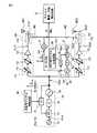
図5は、フェーズドアレイ送信機の一実施例を示すブロック図であり、BIST回路を搭載したフェーズドアレイ送信機、例えば、FM−CWレーダー装置におけるフェーズドアレイ送信機(送受信機)の一例を示すものである。 FIG. 5 is a block diagram showing an embodiment of a phased array transmitter, which shows an example of a phased array transmitter equipped with a BIST circuit, for example, a phased array transmitter (transceiver) in an FM-CW radar device It is.
なお、図5では、説明を簡略化するために2つの送信ユニット101,102、送信アンテナANT1,ANT2およびスイッチSW1,SW2だけが描かれているが、例えば、前述した図1と同様に、実際には、n+1個の送信ユニット101,102,…,10n+1等が設けられている。 In FIG. 5, only two
ここで、FM−CWの送信機は、パルス送信波を使用することなく、周波数変調された連続波を使用して対象物との距離の測定等を行うため、送信時のピーク電力を低く抑えることができ、例えば、送信機を1つの半導体チップとして形成することが可能である。 Here, the transmitter of FM-CW uses a frequency-modulated continuous wave to measure the distance to the object without using a pulse transmission wave, so the peak power during transmission is kept low. For example, the transmitter can be formed as a single semiconductor chip.
図5に示されるように、フェーズドアレイ送信機は、2つ(複数)の送信ユニット101,102、2つの送信アンテナANT1,ANT2、2つのスイッチSW1,SW2、送信用PLL(PLL-TX)2およびBIST用PLL(自己検査用PLL:PLL-BIST)4を含む。 As shown in FIG. 5, the phased array transmitter includes two (plural)
図5に示されるように、フェーズドアレイ送信機は、2つ(複数)の送信ユニット101,102、2つの送信アンテナANT1,ANT2、2つのスイッチSW1,SW2、送信用PLL(PLL-TX)2およびBIST(自己検査)用PLL(PLL-BIST)4を含む。 As shown in FIG. 5, the phased array transmitter includes two (plural)
すなわち、図5と前述した図2の比較から明らかなように、本実施例のフェーズドアレイ送信機では、図2における送信用デジタル制御回路30およびBIST用デジタル制御回路50は、送信用PLL2を制御する制御回路3として纏められている。 That is, as apparent from the comparison between FIG. 5 and FIG. 2 described above, in the phased array transmitter of this embodiment, the transmission
さらに、フェーズドアレイ送信機は、制御回路3、ミキサ(混合器)6、振幅・位相検出回路7、遅延回路(τ)8および第1分周器(1/N)9を含む。ここで、第1分周器9は、固定の分周比Nを有し、送信用PLL2から出力される基準送信信号SotxをN分周して遅延回路8に出力する。 Further, the phased array transmitter includes a
各送信ユニット101,102の構成は、図2および図3を参照して説明したのと同様であり、可変利得アンプ111,112、移相器121,122、パワーアンプ131,132およびカプラ141,142を含む。ミキサ6には、BIST用PLL4からの自己検査用信号Sstが入力され、ミキサ6の出力は、振幅・位相検出回路7に入力される。 The configurations of the
図6は、図5に示すフェーズドアレイ送信機の要部をより詳細に示すブロック図であり、送信用PLL2,BIST用PLL4およびそれらの周辺回路を詳細に示すものである。 FIG. 6 is a block diagram showing in detail the main part of the phased array transmitter shown in FIG. 5, and shows the
また、図7は、図6に示すフェーズドアレイ送信機の動作の一例を説明するためのフローチャートであり、図8は、図6に示すフェーズドアレイ送信機における自己検査処理を説明するための図である。 FIG. 7 is a flowchart for explaining an example of the operation of the phased array transmitter shown in FIG. 6, and FIG. 8 is a diagram for explaining the self-checking process in the phased array transmitter shown in FIG. is there.
図6に示されるように、フェーズドアレイ送信機は、2つ(複数)の送信ユニット101,102、2つの送信アンテナANT1,ANT2、2つのスイッチSW1,SW2、送信用PLL(PLL-TX)2およびBIST(自己検査)用PLL(PLL-BIST)4を含む。 As shown in FIG. 6, the phased array transmitter includes two (plural)
送信用PLL2は、基準クロック発振器21,位相検出器(PD:第1位相検出器)22,ループフィルタ(LF:第1ループフィルタ)23,デジタル制御発振器(DCO:第1発振器)24および第2分周器(1/P)25を含む。 The
ここで、基準クロック発振器21は、前述した図3における送信用基準クロックを発生する送信用基準クロック発振器に対応する。なお、ループフィルタ23は、位相検出器22の出力信号から高周波成分を低減(濾波)する。 Here, the
第2分周器25は、例えば、制御回路3により、その分周比Pが可変制御可能とされている。また、DCO24としては、例えば、アナログの電圧制御発振器(VCO)を適用することもできる。 For example, the
BIST用PLL4は、位相検出器(PD:第2位相検出器)42,ループフィルタ(LF:第2ループフィルタ)43,デジタル制御発振器(DCO:第2発振器)44および第3分周器(1/N)46を含む。 The
ここで、第3分周器46は、第1分周器9と同じ固定の分周比Nを有し、デジタル制御発振器44の出力信号をN分周して位相検出器42にフィードバックするようになっている。また、DCO44として、例えば、アナログの電圧制御発振器(VCO)を適用してもよい。なお、ループフィルタ43は、位相検出器42の出力信号から高周波成分を低減(濾波)する。 Here, the
なお、前述したように、送信用PLL2から出力される基準送信信号Sotxは、第1分周器9によりN分周され、その分周された出力信号が遅延回路8を介してBIST用PLL4の位相検出器42に入力される。すなわち、位相検出器42は、遅延回路8の出力信号および第3分周器46の出力信号を受け取って位相比較(位相検出)を行う。 As described above, the reference transmission signal Sotx output from the
次に、図6および図7を参照して、BIST回路を使用して自己検査を行い、各送信ユニット101,102(101,102,…,10n+1)の出力信号(送信波)の振幅および位相の制御を行う自己検査(自己診断)モードの処理について説明する。 Next, referring to FIG. 6 and FIG. 7, the BIST circuit is used for self-test, and the amplitude of the output signal (transmission wave) of each
図7と前述した図4の比較から明らかなように、本実施例において、自己検査モードが開始しても、ステップST1およびST2の処理は行わず、直接ステップST3に進む。すなわち、本実施例のフェーズドアレイ送信機による自己検査モードでは、送信用PLL(PLL-TX)2およびBIST用PLL(PLL-BIST)4は、固定周波数のクロックを出力することなく、通常動作モードと同様に、周波数変調された連続波を出力し続ける。 As is apparent from the comparison between FIG. 7 and FIG. 4 described above, in this embodiment, even if the self-inspection mode is started, the processing of steps ST1 and ST2 is not performed and the process directly proceeds to step ST3. That is, in the self-inspection mode by the phased array transmitter of the present embodiment, the transmission PLL (PLL-TX) 2 and the BIST PLL (PLL-BIST) 4 do not output a fixed frequency clock, but the normal operation mode. In the same manner as described above, it continues to output a frequency-modulated continuous wave.
そのため、図6および図7に示されるように、自己検査モードが開始すると、ステップST3に進んで、スイッチSW1をオンしてスイッチSW2をオフする。そして、カプラ141により送信ユニット101のパワーアンプ131からの出力信号(被検査信号)Stx1'をミキサ6に入力し、BIST用PLL4からのクロック(自己検査用信号)Sstと混合する。 Therefore, as shown in FIGS. 6 and 7, when the self-inspection mode is started, the process proceeds to step ST3, where the switch SW1 is turned on and the switch SW2 is turned off. Then, the
ここで、本実施例における自己検査処理について、図8を参照して説明する。図8において、参照符号Stx1は、送信波(出力信号)としての送信ユニット101からのユニット送信波を示し、また、Sstは、受信波としてのBIST用PLL4からの自己検査用信号を示す。なお、参照符号fbは、FM−CW方式における受信波の時間遅れに相当し、ミキサ6から出力される送信波と受信波の周波数差であるビート周波数を示す。 Here, the self-inspection processing in the present embodiment will be described with reference to FIG. In FIG. 8, reference symbol Stx1 indicates a unit transmission wave from the
図8に示されるように、本実施例によれば、ミキサ6には、例えば、送信ユニット101からの送信波Stx1、および、BIST用PLL4からの自己検査用信号Sstが入力される。ここで、BIST用PLL4の位相検出器42には、送信用PLL2から出力される基準送信信号Sotxを第1分周器9によりN分周し、さらに、遅延回路8により遅延時間τだけ遅延された信号が入力される。 As shown in FIG. 8, according to the present embodiment, for example, the transmission wave Stx1 from the
また、位相検出器42には、デジタル制御発振器44の出力信号(自己検査用信号)Sstを、第1分周器9の分周比Nと同じ分周比Nを有する第3分周器46によりN分周した信号が入力される。 Further, the
これにより、図8に示されるような、自己検査モードにおいても、通常モードと同様に、周波数差を生じる状態が実現されている。すなわち、図2〜図4を参照して説明したような、自己検査モードにおける固定の周波数(80.000GHzおよび80.001GHz)に設定する制御を不要とすることができる。 As a result, in the self-inspection mode as shown in FIG. 8, a state in which a frequency difference is generated is realized as in the normal mode. That is, the control for setting the fixed frequencies (80.000 GHz and 80.001 GHz) in the self-inspection mode as described with reference to FIGS.
ミキサ6の出力信号(ビート周波数信号)fbは、振幅・位相検出回路7に入力され、送信ユニット101の出力信号(ユニット送信波)Stx1における振幅および位相が検出される。すなわち、振幅・位相検出回路7は、ビート周波数信号fbを、A/D変換およびFFTすることにより、信号Stx1の振幅および位相が計算される。 The output signal (beat frequency signal) fb of the mixer 6 is input to the amplitude /
次に、ステップST4に進み、スイッチSW2をオンしてスイッチSW1をオフし、カプラ142により送信ユニット102のパワーアンプ132からの被検査信号Stx2'をミキサ6に入力して、BIST用PLL4からの自己検査用信号Sstと混合する。このミキサ6からの出力信号は、振幅・位相検出回路7に入力され、送信ユニット102の出力信号Stx2における振幅および位相が検出される。 Next, proceeding to step ST4, the switch SW2 is turned on and the switch SW1 is turned off, and the signal to be tested Stx2 'from the
ここで、送信ユニットの数、すなわち、送信チャネル数がn+1個の場合には、各送信ユニットに対応する1つのスイッチのみをオンして他のスイッチをオフする処理をn+1回繰り返し、各送信ユニットの出力信号における振幅および位相を順に検出する。 Here, when the number of transmission units, that is, the number of transmission channels is n + 1, the process of turning on only one switch corresponding to each transmission unit and turning off the other switches is repeated n + 1 times. The amplitude and phase of the output signal are sequentially detected.
そして、ステップST5に進んで、各チャネル間の振幅差および位相差が基準値内に収まっているかどうかを判定し、基準値内に収まっていないと判定した場合には、ステップST6に進む。 And it progresses to step ST5, it is determined whether the amplitude difference and phase difference between each channel are settled in the reference value, and when it determines with it not being settled in the reference value, it progresses to step ST6.
ステップST6では、振幅・位相検出回路7による検出結果に基づいて、例えば、可変利得アンプ111,112および位相器121,122により、送信ユニットの出力信号における振幅および位相を調整して、ステップST3に戻る。 In step ST6, based on the detection result by the amplitude /
なお、ステップST5において、各チャネル間の振幅差および位相差が基準値内に収まっていると判定した場合、フェーズドアレイ送信機からの放射電波の指向特性が基準を満たしているとして自己検査モードを終了し、通常動作モードを開始する。 In step ST5, when it is determined that the amplitude difference and phase difference between the channels are within the reference value, the self-inspection mode is set assuming that the directional characteristics of the radiated radio waves from the phased array transmitter satisfy the reference. Exit and enter normal operating mode.
ここで、本実施例において、自己検査モードにおいて、位相検出器42に入力する遅延回路8の出力信号および第3分周器46の出力信号は、両方とも送信用PLL2から出力される基準送信信号Sotxに基づくものであり、周波数変調された連続波である。 Here, in this embodiment, in the self-test mode, both the output signal of the
従って、本実施例によれば、自己検査モードを終了して通常モードを開始する場合、例えば、図2〜図4を参照して説明したように、自己検査モードの固定周波数から、通常モードの周波数変調された連続波に切り替える処理が不要となる。 Therefore, according to the present embodiment, when the self-inspection mode is ended and the normal mode is started, for example, as described with reference to FIGS. There is no need to switch to a frequency-modulated continuous wave.
このように、本実施例によれば、BIST用基準クロック発振器(41)およびBIST用PLLを制御するBIST用制御回路(40)が不要となり、消費電力および占有面積を低減することが可能になる。 Thus, according to the present embodiment, the BIST reference clock oscillator (41) and the BIST control circuit (40) for controlling the BIST PLL are not required, and the power consumption and the occupied area can be reduced. .
さらに、本実施例によれば、自己検査モードにおける制御手順を簡易化して検査時間を短縮することができ、また、自己検査モードから通常モードへの切り替えを直ちに行うことが可能になる。 Furthermore, according to the present embodiment, the control procedure in the self-inspection mode can be simplified to shorten the inspection time, and switching from the self-inspection mode to the normal mode can be performed immediately.
図9は、本実施例に係る送受信機の一例を示すブロック図であり、前述した図6に示すフェーズドアレイ送信機に対して、受信機の構成を追加したものに相当する。 FIG. 9 is a block diagram illustrating an example of a transceiver according to the present embodiment, which corresponds to a configuration in which a receiver is added to the phased array transmitter illustrated in FIG. 6 described above.
図9に示されるように、本実施例に係る送受信機501は、図5〜図7を参照して説明した送信機に対して、受信アンテナANT21,ローノイズアンプ211,ミキサ60およびスイッチSW10,SW20が追加されている。 As shown in FIG. 9, the
ここで、前述した自己検査モードでは、スイッチSW10をオンしてスイッチSW10をオフし、ミキサ6の出力信号を振幅・位相検出回路7に入力する。一方、通常モード(受信時)では、スイッチSW10をオフしてスイッチSW10をオンし、ミキサ60の出力信号を振幅・位相検出回路7に入力する。 Here, in the self-inspection mode described above, the switch SW10 is turned on and the switch SW10 is turned off, and the output signal of the mixer 6 is input to the amplitude /
なお、図9では、1つの受信アンテナANT21および1つのローノイズアンプ211のみを示すが、送信ユニット(101,102)と同様に、実際には複数設けられている。また、図9では、受信アンテナANTrxは、送信アンテナ(ANT1,ANT2)と独立に設けられているが、例えば、デュプレクサ等を使用して送受信共用アンテナとすることも可能なのはいうまでもない。 In FIG. 9, only one receiving antenna ANT21 and one
図10は、本実施例に係るレーダー装置の一例を示すブロック図であり、自動車に搭載されたFM−CWレーダー装置500の例を示すものである。 FIG. 10 is a block diagram illustrating an example of a radar apparatus according to the present embodiment, and illustrates an example of an FM-
図10に示されるように、FM−CWレーダー装置500は、自動車制御システム(上位システム)700により制御され、送受信機501,マイコン(信号処理回路)502,CAN通信回路503,電源回路504,送信アンテナANTtxおよび受信アンテナANTrxを含む。 As shown in FIG. 10, the FM-
ここで、CAN通信回路503は、耐ノイズ性の強化を考慮して設計され、相互接続された機器間のデータ転送に使われる規格であるCAN(Controller Area Network:ISO11898およびISO11519として標準化)に基づいた通信を行う回路である。 Here, the
なお、FM−CWレーダー装置500は、例えば、複数の半導体チップ501〜504および送受信アンテナANTtx,ANTrxを1つのパッケージとすることができる。また、例えば、使用する周波数がミリ波からテラヘルツになると、アンテナも含めて1つの半導体チップに形成することもできる。 Note that the FM-
以上において、本実施例は、FM−CWレーダー装置,FM−CWレーダー装置に適用される送受信機および送信機に限定されるものではなく、BIST回路を搭載し、自己検査機能を有する様々な機器に対しても適用することが可能である。 As described above, the present embodiment is not limited to the transceiver and the transmitter applied to the FM-CW radar device and the FM-CW radar device, but various devices having a BIST circuit and having a self-inspection function. It is also possible to apply to.
以上、実施形態を説明したが、ここに記載したすべての例や条件は、発明および技術に適用する発明の概念の理解を助ける目的で記載されたものであり、特に記載された例や条件は発明の範囲を制限することを意図するものではなく、明細書のそのような例の構成は発明の利点および欠点を示すものではない。発明の実施形態を詳細に記載したが、各種の変更、置き換え、変形が発明の精神および範囲を逸脱することなく行えることが理解されるべきである。 Although the embodiment has been described above, all examples and conditions described herein are described for the purpose of helping understanding of the concept of the invention applied to the invention and the technology. It is not intended to limit the scope of the invention, and the construction of such examples in the specification does not indicate the advantages and disadvantages of the invention. Although embodiments of the invention have been described in detail, it should be understood that various changes, substitutions and modifications can be made without departing from the spirit and scope of the invention.
以上の実施例を含む実施形態に関し、さらに、以下の付記を開示する。
(付記1)
基準送信信号を生成する送信用PLLと、
前記送信用PLLを制御する制御回路と、
前記基準送信信号を受け取り、それぞれ増幅および位相制御してユニット送信波を出力する複数の送信ユニットと、
前記基準送信信号に基づく信号を遅延する遅延回路と、
前記遅延回路の出力信号を受け取り、自己検査を行う自己検査用信号を生成する自己検査用PLLと、を有する、
ことを特徴とするフェーズドアレイ送信機。Regarding the embodiment including the above examples, the following supplementary notes are further disclosed.
(Appendix 1)
A transmission PLL for generating a reference transmission signal;
A control circuit for controlling the transmission PLL;
A plurality of transmission units that receive the reference transmission signals and output unit transmission waves with amplification and phase control respectively;
A delay circuit for delaying a signal based on the reference transmission signal;
A self-test PLL that receives the output signal of the delay circuit and generates a self-test signal for performing a self-test,
A phased array transmitter characterized by that.
(付記2)
さらに、前記基準送信信号を受け取り、前記基準送信信号を固定の第1分周比だけ分周して前記遅延回路に出力する第1分周器を有する、
ことを特徴とする付記1に記載のフェーズドアレイ送信機。(Appendix 2)
And a first divider that receives the reference transmission signal, divides the reference transmission signal by a fixed first division ratio, and outputs the divided signal to the delay circuit.
The phased array transmitter according to
(付記3)
さらに、
それぞれの前記ユニット送信波の一部を取り出す複数のカプラと、
前記カプラのいずれか1つの出力信号を選択するスイッチと、
前記スイッチにより選択された前記カプラのいずれか1つの出力信号,および,前記自己検査用PLLからの前記自己検査用信号を混合するミキサと、
前記ミキサの出力を受け取って、それぞれの前記ユニット送信波の振幅および位相を検出する振幅・位相検出回路と、を有する、
ことを特徴とする付記1または付記2に記載のフェーズドアレイ送信機。(Appendix 3)
further,
A plurality of couplers for extracting a part of each unit transmission wave;
A switch for selecting an output signal of any one of the couplers;
A mixer for mixing the output signal of any one of the couplers selected by the switch and the self-inspection signal from the self-inspection PLL;
An amplitude / phase detection circuit that receives the output of the mixer and detects the amplitude and phase of each unit transmission wave;
The phased array transmitter according to
(付記4)
さらに、
それぞれの前記ユニット送信波を放射する、前記送信ユニットに対応して設けられた複数の送信アンテナを有する、
ことを特徴とする付記1乃至付記3のいずれか1項に記載のフェーズドアレイ送信機。(Appendix 4)
further,
A plurality of transmission antennas corresponding to the transmission units, each radiating the unit transmission wave;
The phased array transmitter according to any one of
(付記5)
前記送信用PLLは、
基準クロックを発生する基準クロック発振器と、
前記基準送信信号を受け取り、前記基準送信信号を前記制御回路により可変制御される第2分周比だけ分周する第2分周器と、
前記第2分周器の出力信号,および,前記基準信号を受け取って位相比較を行う第1位相検出器と、
前記第1位相検出器の出力信号から高周波成分を低減する第1ループフィルタと、
前記第1ループフィルタの出力信号に基づいた周波数を有する前記基準送信信号を生成する第1発振器と、を含む、
ことを特徴とする付記1乃至付記4のいずれか1項に記載のフェーズドアレイ送信機。(Appendix 5)
The transmission PLL is:
A reference clock oscillator for generating a reference clock; and
A second frequency divider that receives the reference transmission signal and divides the reference transmission signal by a second division ratio variably controlled by the control circuit;
A first phase detector that receives the output signal of the second divider and the reference signal and performs phase comparison;
A first loop filter that reduces high frequency components from the output signal of the first phase detector;
A first oscillator that generates the reference transmission signal having a frequency based on an output signal of the first loop filter;
The phased array transmitter according to any one of
(付記6)
前記自己検査用PLLは、
前記第1分周器と同じ前記第1分周比だけ分周する第3分周器と、
前記第3分周器の出力信号,および,前記遅延回路の出力信号を受け取って位相比較を行う第2位相検出器と、
前記第2位相検出器の出力信号から高周波成分を低減する第2ループフィルタと、
前記第2ループフィルタの出力信号に基づいた周波数を有する前記自己検査用信号を生成する第2発振器と、を含む、
ことを特徴とする付記1乃至付記5のいずれか1項に記載のフェーズドアレイ送信機。(Appendix 6)
The PLL for self-inspection is
A third frequency divider that divides by the same first frequency division ratio as the first frequency divider;
A second phase detector that receives the output signal of the third frequency divider and the output signal of the delay circuit and performs phase comparison;
A second loop filter for reducing high frequency components from the output signal of the second phase detector;
A second oscillator that generates the self-test signal having a frequency based on an output signal of the second loop filter.
The phased array transmitter according to any one of
(付記7)
前記フェーズドアレイ送信機は、FM−CWレーダー装置におけるフェーズドアレイ送信機である、
ことを特徴とする付記1乃至付記6のいずれか1項に記載のフェーズドアレイ送信機。(Appendix 7)
The phased array transmitter is a phased array transmitter in an FM-CW radar device.
The phased array transmitter according to any one of
(付記8)
付記1乃至付記7のいずれか1項に記載のフェーズドアレイ送信機と、
受信機と、を有する、
ことを特徴とする送受信機。(Appendix 8)
The phased array transmitter according to any one of
And having a receiver,
A transceiver characterized by that.
(付記9)
前記受信機は、
受信アンテナと、
前記受信アンテナからの受信信号を増幅して出力するローノイズアンプと、を有する、
ことを特徴とする付記8に記載の送受信機。(Appendix 9)
The receiver
A receiving antenna;
A low-noise amplifier that amplifies and outputs a received signal from the receiving antenna;
(付記10)
付記8または付記9に記載の送受信機と、
電源回路と、
上位システムとの通信を行う通信回路と、
前記通信回路を介して前記上位システムと通信し、前記送受信機を制御する信号処理回路と、を有する、
ことを特徴とするレーダー装置。(Appendix 10)
The transceiver according to
A power circuit;
A communication circuit for communicating with the host system;
A signal processing circuit that communicates with the host system via the communication circuit and controls the transceiver;
Radar device characterized by that.
2,20 送信用PLL(PLL-TX)
3 制御回路
4,40 BIST用PLL(自己検査用PLL:PLL-BIST)
6,60 ミキサ(混合器)
7 振幅・位相検出回路
8 遅延回路(τ)
9 第1分周器(1/N)
21 基準クロック発振器(送信用基準クロック発振器)
22 位相検出器(PD:第1位相検出器)
23 ループフィルタ(LF:第1ループフィルタ)
24 デジタル制御発振器(DCO:第1発振器)
25 分周器(第2分周器:1/P)
30 送信用デジタル制御回路
41 BIST用基準クロック発振器
42 位相検出器(PD:第2位相検出器)
43 ループフィルタ(LF:第2ループフィルタ)
44 デジタル制御発振器(DCO:第2発振器)
45 分周器(1/Q)
46 第3分周器(1/N)
50 BIST用デジタル制御回路
70 アナログ振幅・位相検出回路
101,102,…,10n+1 送信ユニット
110 基準送信信号生成器
111,112 可変利得アンプ
121,122 移相器
131,132 パワーアンプ
141,142 カプラ
211 ローノイズアンプ
500 レーダー装置
501 送受信機(フェーズドアレイ送受信機)
502 マイコン(信号処理回路)
503 CAN通信回路
504 電源回路
ANT1,ANT2,…,ANTn+1、ANTtx 送信アンテナ
ANTrx 受信アンテナ
SW1,SW2,SW10,SW20 スイッチ2,20 PLL for transmission (PLL-TX)
3
6,60 mixer (mixer)
7 Amplitude /
9 1st frequency divider (1 / N)
21 Reference clock oscillator (Transmission reference clock oscillator)
22 Phase detector (PD: 1st phase detector)
23 Loop filter (LF: 1st loop filter)
24 Digitally controlled oscillator (DCO: first oscillator)
25 divider (second divider: 1 / P)
30 Digital Control Circuit for
43 Loop filter (LF: 2nd loop filter)
44 Digitally controlled oscillator (DCO: second oscillator)
45 frequency divider (1 / Q)
46 Third divider (1 / N)
50 Digital control circuit for
101,102, ..., 10n + 1 transmission unit
110 reference transmission signal generator
111, 112 Variable gain amplifier
121, 122 Phase shifter
131, 132 Power amplifier
141, 142 coupler
211 Low noise amplifier
500 radar equipment
501 transceiver (phased array transceiver)
502 microcomputer (signal processing circuit)
503 CAN communication circuit
504 Power circuit
ANT1, ANT2, ..., ANTn + 1, ANTtx transmit antenna
ANTrx receive antenna
SW1, SW2, SW10, SW20 switch
Claims (7)
Translated fromJapanese前記送信用PLLを制御する制御回路と、
前記基準送信信号を受け取り、それぞれ増幅および位相制御してユニット送信波を出力する複数の送信ユニットと、
前記基準送信信号に基づく信号を遅延する遅延回路と、
前記遅延回路の出力信号を受け取り、自己検査を行う自己検査用信号を生成する自己検査用PLLと、を有する、
ことを特徴とするフェーズドアレイ送信機。A transmission PLL for generating a reference transmission signal;
A control circuit for controlling the transmission PLL;
A plurality of transmission units that receive the reference transmission signals and output unit transmission waves with amplification and phase control respectively;
A delay circuit for delaying a signal based on the reference transmission signal;
A self-test PLL that receives the output signal of the delay circuit and generates a self-test signal for performing a self-test,
A phased array transmitter characterized by that.
ことを特徴とする請求項1に記載のフェーズドアレイ送信機。And a first divider that receives the reference transmission signal, divides the reference transmission signal by a fixed first division ratio, and outputs the divided signal to the delay circuit.
The phased array transmitter according to claim 1.
それぞれの前記ユニット送信波の一部を取り出す複数のカプラと、
前記カプラのいずれか1つの出力信号を選択するスイッチと、
前記スイッチにより選択された前記カプラのいずれか1つの出力信号,および,前記自己検査用PLLからの前記自己検査用信号を混合するミキサと、
前記ミキサの出力を受け取って、それぞれの前記ユニット送信波の振幅および位相を検出する振幅・位相検出回路と、を有する、
ことを特徴とする請求項1または請求項2に記載のフェーズドアレイ送信機。further,
A plurality of couplers for extracting a part of each unit transmission wave;
A switch for selecting an output signal of any one of the couplers;
A mixer for mixing the output signal of any one of the couplers selected by the switch and the self-inspection signal from the self-inspection PLL;
An amplitude / phase detection circuit that receives the output of the mixer and detects the amplitude and phase of each unit transmission wave;
The phased array transmitter according to claim 1, wherein the phased array transmitter is provided.
基準クロックを発生する基準クロック発振器と、
前記基準送信信号を受け取り、前記基準送信信号を前記制御回路により可変制御される第2分周比だけ分周する第2分周器と、
前記第2分周器の出力信号,および,前記基準信号を受け取って位相比較を行う第1位相検出器と、
前記第1位相検出器の出力信号から高周波成分を低減する第1ループフィルタと、
前記第1ループフィルタの出力信号に基づいた周波数を有する前記基準送信信号を生成する第1発振器と、を含む、
ことを特徴とする請求項1乃至請求項3のいずれか1項に記載のフェーズドアレイ送信機。The transmission PLL is:
A reference clock oscillator for generating a reference clock; and
A second frequency divider that receives the reference transmission signal and divides the reference transmission signal by a second division ratio variably controlled by the control circuit;
A first phase detector that receives the output signal of the second divider and the reference signal and performs phase comparison;
A first loop filter that reduces high frequency components from the output signal of the first phase detector;
A first oscillator that generates the reference transmission signal having a frequency based on an output signal of the first loop filter;
The phased array transmitter according to any one of claims 1 to 3, wherein the phased array transmitter is provided.
前記第1分周器と同じ前記第1分周比だけ分周する第3分周器と、
前記第3分周器の出力信号,および,前記遅延回路の出力信号を受け取って位相比較を行う第2位相検出器と、
前記第2位相検出器の出力信号から高周波成分を低減する第2ループフィルタと、
前記第2ループフィルタの出力信号に基づいた周波数を有する前記自己検査用信号を生成する第2発振器と、を含む、
ことを特徴とする請求項1乃至請求項4のいずれか1項に記載のフェーズドアレイ送信機。The PLL for self-inspection is
A third frequency divider that divides by the same first frequency division ratio as the first frequency divider;
A second phase detector that receives the output signal of the third frequency divider and the output signal of the delay circuit and performs phase comparison;
A second loop filter for reducing high frequency components from the output signal of the second phase detector;
A second oscillator that generates the self-test signal having a frequency based on an output signal of the second loop filter.
The phased array transmitter according to claim 1, wherein the phased array transmitter is provided.
受信機と、を有する、
ことを特徴とする送受信機。A phased array transmitter according to any one of claims 1 to 5,
And having a receiver,
A transceiver characterized by that.
電源回路と、
上位システムとの通信を行う通信回路と、
前記通信回路を介して前記上位システムと通信し、前記送受信機を制御する信号処理回路と、を有する、
ことを特徴とするレーダー装置。A transceiver according to claim 6;
A power circuit;
A communication circuit for communicating with the host system;
A signal processing circuit that communicates with the host system via the communication circuit and controls the transceiver;
Radar device characterized by that.
Priority Applications (2)
| Application Number | Priority Date | Filing Date | Title |
|---|---|---|---|
| JP2014073328AJP6252314B2 (en) | 2014-03-31 | 2014-03-31 | Phased array transmitter, transceiver and radar equipment |
| US14/631,026US9817106B2 (en) | 2014-03-31 | 2015-02-25 | Phased-array transmitter, transceiver, and radar apparatus |
Applications Claiming Priority (1)
| Application Number | Priority Date | Filing Date | Title |
|---|---|---|---|
| JP2014073328AJP6252314B2 (en) | 2014-03-31 | 2014-03-31 | Phased array transmitter, transceiver and radar equipment |
Publications (2)
| Publication Number | Publication Date |
|---|---|
| JP2015194448Atrue JP2015194448A (en) | 2015-11-05 |
| JP6252314B2 JP6252314B2 (en) | 2017-12-27 |
Family
ID=54190013
Family Applications (1)
| Application Number | Title | Priority Date | Filing Date |
|---|---|---|---|
| JP2014073328AExpired - Fee RelatedJP6252314B2 (en) | 2014-03-31 | 2014-03-31 | Phased array transmitter, transceiver and radar equipment |
Country Status (2)
| Country | Link |
|---|---|
| US (1) | US9817106B2 (en) |
| JP (1) | JP6252314B2 (en) |
Cited By (9)
| Publication number | Priority date | Publication date | Assignee | Title |
|---|---|---|---|---|
| JP2017158086A (en)* | 2016-03-03 | 2017-09-07 | 富士通株式会社 | Active phased array transmitter, active phased array receiver and active phased-array transmitter-receiver |
| CN107976658A (en)* | 2016-10-25 | 2018-05-01 | 德克萨斯仪器股份有限公司 | The field monitoring of analog signal in radar system |
| JP2019503491A (en)* | 2016-02-12 | 2019-02-07 | ローベルト ボッシュ ゲゼルシャフト ミット ベシュレンクテル ハフツング | Radar sensor for car driver assist system |
| KR20190026245A (en)* | 2017-09-04 | 2019-03-13 | 재단법인대구경북과학기술원 | Actice electronically scanned array radar and method for generating output radar signal using the same |
| WO2019059217A1 (en)* | 2017-09-22 | 2019-03-28 | ミツミ電機株式会社 | Radar device |
| JP2021032658A (en)* | 2019-08-22 | 2021-03-01 | 株式会社デンソー | Self-diagnosis device |
| JP2021110589A (en)* | 2020-01-08 | 2021-08-02 | 株式会社デンソー | Self-diagnosis device |
| JP2021110588A (en)* | 2020-01-08 | 2021-08-02 | 株式会社デンソー | Self-diagnosis device |
| US12095373B2 (en) | 2021-02-26 | 2024-09-17 | Denso Corporation | Power conversion apparatus |
Families Citing this family (13)
| Publication number | Priority date | Publication date | Assignee | Title |
|---|---|---|---|---|
| WO2018028771A1 (en)* | 2016-08-09 | 2018-02-15 | Telefonaktiebolaget Lm Ericsson (Publ) | Frequency synthesizer |
| EP3306838B8 (en)* | 2016-10-06 | 2019-06-05 | Rohde & Schwarz GmbH & Co. KG | System and method for testing antenna arrays |
| US9866259B1 (en) | 2016-11-23 | 2018-01-09 | Infineon Technologies Ag | Transmitter/receiver module for millimeter wave 5G MIMO communication systems |
| CA3009207A1 (en) | 2017-06-22 | 2018-12-22 | Maple Microsystems Inc. | Methods and systems for forming a wireless sensor network |
| CN107329121B (en)* | 2017-07-27 | 2023-04-14 | 南京信息工程大学 | Transmitting Circuit Used in Experimental Measurement of S-band Precipitation Particle Scattering |
| DE102018216538A1 (en)* | 2018-09-27 | 2020-04-02 | Robert Bosch Gmbh | Radar sensor with synchronized high-frequency components |
| CN109541561A (en)* | 2018-11-21 | 2019-03-29 | 上海航天电子通讯设备研究所 | A kind of delay component and phased-array radar |
| CN109901125B (en)* | 2019-03-11 | 2021-07-23 | 中国电子科技集团公司第三十八研究所 | An airborne two-dimensional active phased array radar antenna calibration device and method |
| US11385322B2 (en) | 2019-04-29 | 2022-07-12 | Ay Dee Kay Llc | Switchable FMCW/PMCW radar transceiver |
| JP7444004B2 (en) | 2020-09-15 | 2024-03-06 | 株式会社デンソー | injection control device |
| JP7514718B2 (en)* | 2020-10-01 | 2024-07-11 | 株式会社デンソー | Radar Equipment |
| US11218153B1 (en)* | 2020-10-29 | 2022-01-04 | Nxp B.V. | Configurable built-in self-test for an all digital phase locked loop |
| CN114123979B (en)* | 2022-01-25 | 2022-05-03 | 电子科技大学 | Terahertz full-duplex common local oscillator solid-state front-end transmitting circuit |
Citations (4)
| Publication number | Priority date | Publication date | Assignee | Title |
|---|---|---|---|---|
| JPH02184786A (en)* | 1989-01-11 | 1990-07-19 | Mitsubishi Electric Corp | Method and device for antenna test |
| JPH07198826A (en)* | 1993-12-29 | 1995-08-01 | Fujitsu Ten Ltd | Radar apparatus provided with self-diagnostic function and plate antenna |
| US20080068256A1 (en)* | 2005-01-13 | 2008-03-20 | Niedzwiecki Joshua D | Stepped Frequency Radar |
| JP2011130174A (en)* | 2009-12-17 | 2011-06-30 | Fujitsu Ltd | Communication device |
Family Cites Families (4)
| Publication number | Priority date | Publication date | Assignee | Title |
|---|---|---|---|---|
| JP2600770B2 (en) | 1988-03-08 | 1997-04-16 | 日本電気株式会社 | Phased array radar device |
| JP2748063B2 (en) | 1992-03-19 | 1998-05-06 | 本田技研工業株式会社 | Time-division FM radar system |
| JPH10186025A (en) | 1996-12-25 | 1998-07-14 | Mitsubishi Electric Corp | FM-CW radar |
| US20140225635A1 (en)* | 2013-02-11 | 2014-08-14 | Qualcomm Incorporated | All-digital phase locked loop self test system |
- 2014
- 2014-03-31JPJP2014073328Apatent/JP6252314B2/ennot_activeExpired - Fee Related
- 2015
- 2015-02-25USUS14/631,026patent/US9817106B2/enactiveActive
Patent Citations (4)
| Publication number | Priority date | Publication date | Assignee | Title |
|---|---|---|---|---|
| JPH02184786A (en)* | 1989-01-11 | 1990-07-19 | Mitsubishi Electric Corp | Method and device for antenna test |
| JPH07198826A (en)* | 1993-12-29 | 1995-08-01 | Fujitsu Ten Ltd | Radar apparatus provided with self-diagnostic function and plate antenna |
| US20080068256A1 (en)* | 2005-01-13 | 2008-03-20 | Niedzwiecki Joshua D | Stepped Frequency Radar |
| JP2011130174A (en)* | 2009-12-17 | 2011-06-30 | Fujitsu Ltd | Communication device |
Cited By (16)
| Publication number | Priority date | Publication date | Assignee | Title |
|---|---|---|---|---|
| JP2019503491A (en)* | 2016-02-12 | 2019-02-07 | ローベルト ボッシュ ゲゼルシャフト ミット ベシュレンクテル ハフツング | Radar sensor for car driver assist system |
| JP2017158086A (en)* | 2016-03-03 | 2017-09-07 | 富士通株式会社 | Active phased array transmitter, active phased array receiver and active phased-array transmitter-receiver |
| US11796634B2 (en) | 2016-10-25 | 2023-10-24 | Texas Instruments Incorporated | Field monitoring of analog signals in a radar system |
| CN107976658A (en)* | 2016-10-25 | 2018-05-01 | 德克萨斯仪器股份有限公司 | The field monitoring of analog signal in radar system |
| CN107976658B (en)* | 2016-10-25 | 2024-02-27 | 德克萨斯仪器股份有限公司 | In-situ monitoring of analog signals in radar systems |
| KR20190026245A (en)* | 2017-09-04 | 2019-03-13 | 재단법인대구경북과학기술원 | Actice electronically scanned array radar and method for generating output radar signal using the same |
| KR102037476B1 (en) | 2017-09-04 | 2019-10-28 | 재단법인대구경북과학기술원 | Actice electronically scanned array radar and method for generating output radar signal using the same |
| WO2019059217A1 (en)* | 2017-09-22 | 2019-03-28 | ミツミ電機株式会社 | Radar device |
| JP2019056670A (en)* | 2017-09-22 | 2019-04-11 | ミツミ電機株式会社 | Radar device |
| JP2021032658A (en)* | 2019-08-22 | 2021-03-01 | 株式会社デンソー | Self-diagnosis device |
| JP7279580B2 (en) | 2019-08-22 | 2023-05-23 | 株式会社デンソー | self-diagnostic device |
| JP2021110589A (en)* | 2020-01-08 | 2021-08-02 | 株式会社デンソー | Self-diagnosis device |
| JP7327169B2 (en) | 2020-01-08 | 2023-08-16 | 株式会社デンソー | self-diagnostic device |
| JP7327168B2 (en) | 2020-01-08 | 2023-08-16 | 株式会社デンソー | self-diagnostic device |
| JP2021110588A (en)* | 2020-01-08 | 2021-08-02 | 株式会社デンソー | Self-diagnosis device |
| US12095373B2 (en) | 2021-02-26 | 2024-09-17 | Denso Corporation | Power conversion apparatus |
Also Published As
| Publication number | Publication date |
|---|---|
| US20150276919A1 (en) | 2015-10-01 |
| US9817106B2 (en) | 2017-11-14 |
| JP6252314B2 (en) | 2017-12-27 |
Similar Documents
| Publication | Publication Date | Title |
|---|---|---|
| JP6252314B2 (en) | Phased array transmitter, transceiver and radar equipment | |
| US10983193B2 (en) | Communication unit, integrated circuits and methods for cascading integrated circuits | |
| US11621757B2 (en) | System and method for a multi-beam beamforming front-end architecture for wireless transceivers | |
| JP7066015B2 (en) | Antenna device and radar device | |
| US9444140B2 (en) | Multi-element antenna beam forming configurations for millimeter wave systems | |
| US6414631B1 (en) | Time sharing type multi-beam radar apparatus having alternately arranged transmitting antennas and receiving antennas | |
| US9998170B2 (en) | Active phased array transmitter, active phased array receiver, and active phased array transceiver | |
| US11349208B2 (en) | Antenna apparatus with switches for antenna array calibration | |
| US10469183B1 (en) | Antenna device and method for calibrating antenna device | |
| US20110115665A1 (en) | Beam steering system of phased array antenna using frequency | |
| JP7319378B2 (en) | dual-polarized millimeter-wave front-end integrated circuit | |
| US12123943B2 (en) | Radar device | |
| US10979150B2 (en) | Method of testing RF integrated circuit | |
| Repeta et al. | A scalable 256-element E-band phased-array transceiver for broadband communications | |
| JP2021021576A (en) | Radar device | |
| US10630460B2 (en) | Microwave communication apparatus with multi-channel radio frequency module and continuous beam scanning and method for electronic beam scanning | |
| KR101997988B1 (en) | Hybrid Type Transceiver for Broadband Large Area Beamforming | |
| US11112489B2 (en) | Radar systems and methods having isolator driven mixer | |
| US20210055376A1 (en) | Device and method for transmitting a radar signal | |
| Salarpour et al. | A mm-wave MIMO transmitter with a digital beam steering capability using CMOS all-digital phase-locked loop chips | |
| WO2018163682A1 (en) | Phase shifter, communication instrument and phase shift method | |
| CN119199760B (en) | A phased array radar jammer system with multi-beam reception and narrow beam transmission | |
| JP6206011B2 (en) | Phased array radio equipment | |
| WO2024263409A1 (en) | Precoding radar receive signals | |
| WO2024257209A1 (en) | Phased array device |
Legal Events
| Date | Code | Title | Description |
|---|---|---|---|
| A621 | Written request for application examination | Free format text:JAPANESE INTERMEDIATE CODE: A621 Effective date:20160804 | |
| A977 | Report on retrieval | Free format text:JAPANESE INTERMEDIATE CODE: A971007 Effective date:20170516 | |
| A131 | Notification of reasons for refusal | Free format text:JAPANESE INTERMEDIATE CODE: A131 Effective date:20170613 | |
| A521 | Request for written amendment filed | Free format text:JAPANESE INTERMEDIATE CODE: A523 Effective date:20170627 | |
| TRDD | Decision of grant or rejection written | ||
| A01 | Written decision to grant a patent or to grant a registration (utility model) | Free format text:JAPANESE INTERMEDIATE CODE: A01 Effective date:20171031 | |
| A61 | First payment of annual fees (during grant procedure) | Free format text:JAPANESE INTERMEDIATE CODE: A61 Effective date:20171113 | |
| R150 | Certificate of patent or registration of utility model | Ref document number:6252314 Country of ref document:JP Free format text:JAPANESE INTERMEDIATE CODE: R150 | |
| LAPS | Cancellation because of no payment of annual fees |