JP2015165745A - Power supply circuit - Google Patents
Power supply circuitDownload PDFInfo
- Publication number
- JP2015165745A JP2015165745AJP2014040213AJP2014040213AJP2015165745AJP 2015165745 AJP2015165745 AJP 2015165745AJP 2014040213 AJP2014040213 AJP 2014040213AJP 2014040213 AJP2014040213 AJP 2014040213AJP 2015165745 AJP2015165745 AJP 2015165745A
- Authority
- JP
- Japan
- Prior art keywords
- power supply
- fet
- switching element
- circuit
- battery
- Prior art date
- Legal status (The legal status is an assumption and is not a legal conclusion. Google has not performed a legal analysis and makes no representation as to the accuracy of the status listed.)
- Pending
Links
Images


Landscapes
- Protection Of Static Devices (AREA)
- Charge And Discharge Circuits For Batteries Or The Like (AREA)
- Inverter Devices (AREA)
Abstract
Translated fromJapaneseDescription
Translated fromJapanese本発明は、直流電源の電圧を負荷へ供給する回路に関し、特に、電源が逆接続された場合の保護機能を備えた電源供給回路に関する。 The present invention relates to a circuit for supplying a voltage of a DC power supply to a load, and particularly to a power supply circuit having a protection function when a power supply is reversely connected.
直流電源と負荷を接続する際に、負荷に対して直流電源の正極と負極が逆に接続される、いわゆる逆接続が行われると、回路に大電流が流れて素子が破壊することがある。このような逆接続に対する保護機能を備えた電源供給回路として、たとえば、後記の特許文献1〜3に記載されたものが知られている。 When the DC power supply and the load are connected, if the positive and negative electrodes of the DC power supply are reversely connected to the load, so-called reverse connection is performed, a large current may flow through the circuit and the element may be destroyed. As a power supply circuit having a protection function against such reverse connection, for example, those described in
特許文献1では、直流電源の正極とグランドとの間に、第1パワートランジスタと負荷とが直列に接続された電源供給回路において、第1パワートランジスタと直列に、保護用の第2パワートランジスタが設けられている。直流電源が逆接続された場合は、第2パワートランジスタがOFF状態となって、回路に大電流が流れるのを阻止する。 In
特許文献2では、負荷と、第1ダイオードが並列接続された第1FETと、第2ダイオードが並列接続された第2FETとが、直流電源の正極とグランドとの間に直列に接続されている。直流電源が逆接続された場合は、第1FETと第2FETが共にOFF状態となり、かつ、第1ダイオードが電源に対して逆方向となって、電子機器の破壊が防止される。 In
特許文献3では、直流電源の正極と制御回路とを結ぶ電源ライン上に、第1ダイオードが並列接続された第1FETと、第2ダイオードが並列接続された第2FETとが、直列に設けられている。直流電源が逆接続された場合は、第1FETと第2FETが共にOFF状態となり、かつ、第1ダイオードが電源に対して逆方向となって、制御回路の破壊が防止される。 In
図7は、電源の逆接続に対する保護機能を備えた、従来の電源供給回路の一例を示している。電源供給回路300は、自動車に搭載されており、直流電源であるバッテリBの電圧を、電動パワーステアリング用のモータ(図示省略)へ供給するための回路である。電源供給回路300には、制御部1、電源回路2、インバータ回路3、FET(電界効果トランジスタ)41、FET42、FET駆動回路5、ダイオード6、および電源ラインL1〜L4が備わっている。バッテリBの「+」の記号は正極を表し、「−」の記号は負極を表している。 FIG. 7 shows an example of a conventional power supply circuit having a protection function against reverse connection of power. The
FET41、42は、バッテリBの正極とインバータ回路3との間の電源ラインL1上に、直列に接続されている。FET41は、バッテリBからインバータ回路3への通電・非通電を切り替える電路開閉用のスイッチング素子である。FET42は、バッテリBの逆接続時に、インバータ回路3を含むパワー系回路を保護する保護用のスイッチング素子である。FET41、42は、それぞれダイオードD1、D2を有している。これらのダイオードは、FETのソース・ドレイン間の寄生ダイオードである。ダイオードD1は、バッテリBに対して逆方向となるように設けられている。ダイオードD2は、バッテリBに対して順方向となるように設けられている。ダイオード6は、バッテリBの逆接続時に、制御部1を含む信号系回路を保護する保護用のダイオードである。このダイオード6は、バッテリBに対して順方向となるように、バッテリBの正極と電源回路2との間の電源ラインL3上に設けられている。 The
電源回路2は、車両に備わるイグニッションスイッチIGから与えられる制御信号により動作し、ダイオード6を介して供給されるバッテリBの電圧を降圧して制御部1へ供給する。制御部1は、図示しないトルクセンサから入力される操舵トルク値に基づいて、モータを駆動するためのPWM(パルス幅変調)信号を生成し、これをインバータ回路3へ出力する。また、制御部1は、FET駆動回路5に対して、FET41、42のオン・オフを制御するための制御信号を出力する。FET駆動回路5は、この制御信号に応じて、FET41、42をオンまたはオフさせる。 The
イグニッションスイッチIGがオンして、電源回路2から制御部1へ電源電圧が供給されると、制御部1が動作を開始する。そして、制御部1からの制御信号に基づいて、FET駆動回路5がFET41、42をオン状態にし、かつ、制御部1からインバータ回路3へPWM信号が与えられると、インバータ回路3が動作する。インバータ回路3の動作によって、図8に点線で示すような電流経路が形成され、インバータ回路3からモータに電流が流れて(電流経路は省略)、モータが駆動される。 When the ignition switch IG is turned on and the power supply voltage is supplied from the
図9は、電源供給回路300が動作していない状態で、バッテリBが逆接続された場合を示している。このとき、FET42のダイオードD2と、ダイオード6は、共にバッテリBに対して逆方向となる。その結果、点線で示したように、逆接続されたバッテリBの正極から、インバータ回路3とFET41のダイオードD1を経由して、バッテリBの負極へ向う電流経路は、FET42のダイオードD2により遮断される。また、逆接続されたバッテリBの正極から、制御部1と電源回路2を経由して、バッテリBの負極へ向う電流経路は、ダイオード6により遮断される。 FIG. 9 shows a case where the battery B is reversely connected while the
このようにして、バッテリBが逆接続された場合でも、FET42のダイオードD2によって、インバータ回路3を含むパワー系回路に大電流が流れるのを阻止することができる。また、ダイオード6によって、制御部1を含む信号系回路に大電流が流れるのを阻止することができる。 Thus, even when the battery B is reversely connected, the diode D2 of the
図7に示した従来の電源供給回路300では、逆接続保護用の素子として、FET42のほかにダイオード6を用いているため、部品点数が増加する。また、電源供給回路300の動作中は、ダイオード6で順方向電圧降下が生じるため、バッテリBから電源回路2へ供給される電圧が減少するという問題がある。 In the conventional
本発明の課題は、逆接続保護用の素子の数を低減でき、かつ、直流電源の供給電圧が減少するのを抑制できる電源供給回路を提供することにある。 An object of the present invention is to provide a power supply circuit that can reduce the number of elements for protection against reverse connection and can suppress a decrease in supply voltage of a DC power supply.
本発明に係る電源供給回路は、直流電源の正極と負荷との間に設けられる第1電源ラインと、直流電源の負極と負荷との間に設けられる第2電源ラインと、第1電源ライン上に設けられ、直流電源から負荷への通電・非通電を切り替える電路開閉用の第1スイッチング素子と、この第1スイッチング素子と直流電源の正極との間にあって、第1スイッチング素子と直列に接続された、逆接続保護用の第2スイッチング素子と、直流電源に対して逆方向となるように、第1スイッチング素子に並列接続された第1ダイオードと、直流電源に対して順方向となるように、第2スイッチング素子に並列接続された第2ダイオードと、第1スイッチング素子および第2スイッチング素子のオン・オフを制御する制御部と、直流電源の正極と制御部との間に設けられる第3電源ラインと、直流電源の負極と制御部との間に設けられる第4電源ラインとを備えている。そして、本発明においては、第3電源ラインが、第2スイッチング素子を介して、直流電源の正極に接続されている。 A power supply circuit according to the present invention includes a first power supply line provided between a positive electrode of a DC power supply and a load, a second power supply line provided between a negative electrode of the DC power supply and a load, and the first power supply line. Provided between the first switching element for switching between energization and de-energization from the DC power supply to the load, and between the first switching element and the positive electrode of the DC power supply, and connected in series with the first switching element. In addition, the second switching element for protection against reverse connection and the first diode connected in parallel to the first switching element so as to be in the reverse direction with respect to the DC power supply and the forward direction with respect to the DC power supply A second diode connected in parallel to the second switching element, a control unit for controlling on / off of the first switching element and the second switching element, a positive electrode of the DC power source, and a control unit A third power supply line provided, and a fourth power supply line provided between the anode and the control unit of the DC power supply. In the present invention, the third power supply line is connected to the positive electrode of the DC power supply via the second switching element.
この構成によると、直流電源が逆接続された場合に、第2スイッチング素子に並列接続されている第2ダイオードが、直流電源に対して逆方向となる。一方、第1スイッチング素子に並列接続されている第1ダイオードは、直流電源に対して順方向となる。そして、逆接続された直流電源の正極から、負荷と第1スイッチング素子の第1ダイオードを経由して、直流電源の負極へ向う電流経路は、第2スイッチング素子の第2ダイオードにより遮断される。また、逆接続された直流電源の正極から、制御部を経由して、直流電源の負極へ向う電流経路も、第2スイッチング素子の第2ダイオードにより遮断される。したがって、直流電源の逆接続時に、第2ダイオードによって、負荷を含むパワー系回路と制御部を含む信号系回路の双方を、大電流から保護することができる。このため、図7における信号系回路保護用のダイオード6が不要となり、逆接続保護用の素子の数を低減することができる。また、ダイオード6を用いた場合の順方向電圧降下が生じないため、直流電源から制御部へ供給される電圧が減少するのを抑制することができる。 According to this configuration, when the DC power supply is reversely connected, the second diode connected in parallel to the second switching element is in the reverse direction with respect to the DC power supply. On the other hand, the first diode connected in parallel to the first switching element is in the forward direction with respect to the DC power supply. The current path from the positive electrode of the DC power source connected in reverse to the negative electrode of the DC power source via the load and the first diode of the first switching element is blocked by the second diode of the second switching element. The current path from the reversely connected positive electrode of the direct current power source to the negative electrode of the direct current power source via the control unit is also blocked by the second diode of the second switching element. Therefore, when the DC power supply is reversely connected, both the power system circuit including the load and the signal system circuit including the control unit can be protected from a large current by the second diode. For this reason, the
本発明において、第1スイッチング素子と第2スイッチング素子を、第2電源ライン上に設けてもよい。この場合、第2スイッチング素子は、第1スイッチング素子と直流電源の負極との間に設けられ、第4電源ラインが、第2スイッチング素子を介して、直流電源の負極に接続される。 In the present invention, the first switching element and the second switching element may be provided on the second power supply line. In this case, the second switching element is provided between the first switching element and the negative electrode of the DC power supply, and the fourth power supply line is connected to the negative electrode of the DC power supply via the second switching element.
本発明において、第1スイッチング素子および第2スイッチング素子は、それぞれMOSFETからなり、第1ダイオードおよび第2ダイオードは、それぞれMOSFETのソース・ドレイン間に備わる寄生ダイオードであってもよい。 In the present invention, each of the first switching element and the second switching element may be a MOSFET, and each of the first diode and the second diode may be a parasitic diode provided between the source and drain of the MOSFET.
本発明において、第3電源ラインと制御部との間に、直流電源の電圧を降圧して制御部へ供給する電源回路が設けられていてもよい。 In the present invention, a power supply circuit that steps down the voltage of the DC power supply and supplies the voltage to the control unit may be provided between the third power supply line and the control unit.
本発明において、負荷は、モータ駆動用のインバータ回路であってもよい。 In the present invention, the load may be an inverter circuit for driving a motor.
本発明によれば、逆接続保護用の素子の数を低減でき、かつ、直流電源の供給電圧が減少するのを抑制できる電源供給回路を提供することができる。 ADVANTAGE OF THE INVENTION According to this invention, the power supply circuit which can reduce the number of elements for reverse connection protection, and can suppress that the supply voltage of DC power supply reduces can be provided.
以下、本発明の実施形態につき、図面を参照しながら説明する。各図において、同一部分または対応部分には、同一符号を付してある。 Hereinafter, embodiments of the present invention will be described with reference to the drawings. In each drawing, the same reference numerals are given to the same parts or corresponding parts.
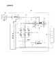
まず、本発明の実施形態に係る電源供給回路の構成を、図1を参照しながら説明する。図1において、電源供給回路100は、自動車に搭載されており、直流電源であるバッテリBの電圧を、電動パワーステアリング用のモータ(図示省略)へ供給するための回路である。電源供給回路100には、制御部1、電源回路2、インバータ回路3、FET41、FET42、FET駆動回路5、および電源ラインL1〜L4が備わっている。バッテリBの「+」の記号は正極を表し、「−」の記号は負極を表している。 First, the configuration of a power supply circuit according to an embodiment of the present invention will be described with reference to FIG. In FIG. 1, a
バッテリBの正極とインバータ回路3との間の電源ラインL1(第1電源ライン)上には、FET41(第1スイッチング素子)およびFET42(第2スイッチング素子)が設けられている。FET41は、バッテリBからインバータ回路3への通電・非通電を切り替える電路開閉用のスイッチング素子である。FET42は、バッテリBの逆接続時に、制御部1やインバータ回路3等を保護する保護用のスイッチング素子である。これらのFET41、42は、Nチャンネル型のMOSFETからなる。 On the power supply line L1 (first power supply line) between the positive electrode of the battery B and the
FET41は、FET42よりもインバータ回路3側に設けられている。FET42は、FET41とバッテリBの正極との間にあって、FET41と直列に接続されている。FET41のソースsは、インバータ回路3の一端に接続されており、FET41のドレインdは、FET42のドレインdと接続されている。FET42のソースsは、バッテリBの正極に接続されている。FET41、42の各ゲートgは、FET駆動回路5に接続されている。 The
FET41には、バッテリBに対して逆方向となるようにダイオードD1(第1ダイオード)が並列に接続されている。このダイオードD1は、FET41のソースs・ドレインd間に備わる寄生ダイオードである。FET42には、バッテリBに対して順方向となるようにダイオードD2(第2ダイオード)が並列に接続されている。このダイオードD2は、FET42のソースs・ドレインd間に備わる寄生ダイオードである。 A diode D1 (first diode) is connected in parallel to the
バッテリBの正極と制御部1との間には、バッテリBの電圧を制御部1へ供給するための電源ラインL3(第3電源ライン)が設けられている。詳しくは、電源ラインL3の一端は、FET41とFET42との接続点Paに接続されていて、FET42を介してバッテリBの正極に接続されている。電源ラインL3の他端は、電源回路2を介して制御部1と接続されている。 Between the positive electrode of the battery B and the
電源回路2は、車両に備わるイグニッションスイッチIGから与えられる制御信号により動作し、FET42を介して供給されるバッテリBの電圧を降圧して制御部1へ供給する。たとえば、電源回路2として、バッテリBの12Vの電圧を5Vの電圧に降圧するレギュレータ回路を用いることができる。 The
インバータ回路3は、6個のスイッチング素子Q1〜Q6およびシャント抵抗Rを有する公知の3相ブリッジ回路から構成される。スイッチング素子Q1〜Q6は、並列接続された寄生ダイオードを有するMOSFETからなり、制御部1から与えられるPWM(パルス幅変調)信号によりオン・オフ動作を行う。これにより、バッテリBからインバータ回路3を通ってモータに電流が流れ、モータが回転する。シャント抵抗Rは、モータに流れる相電流を検出するための抵抗であって、図示しない電流検出回路に接続されている。インバータ回路3の一端は、前述した電源ラインL1に接続されている。インバータ回路3の他端は、バッテリBの負極とインバータ回路3との間に設けられた電源ラインL2(第2電源ライン)に接続されている。インバータ回路3は、本発明における「負荷」の一例である。 The
制御部1は、CPUやPWM信号生成回路などから構成されている。制御部1には、図示しないトルクセンサから、操舵量に応じた操舵トルク値が入力される。制御部1は、この操舵トルク値に基づいて、モータを駆動するためのPWM信号を生成し、これをインバータ回路3の各スイッチング素子Q1〜Q6のゲートへ出力する。また、制御部1は、FET駆動回路5に対して、FET41、42のオン・オフを制御するための制御信号を出力する。制御部1には、バッテリBの負極と制御部1との間に設けられた電源ラインL4(第4電源ライン)が接続されている。 The
FET駆動回路5は、制御部1からの制御信号に応じて、FET41、42をオンまたはオフさせるための駆動信号を、FET41、42のゲートgへ出力する。詳しくは、FET駆動回路5は、FET41、42をオンさせる場合は、ハイレベルの駆動信号を出力し、FET41、42をオフさせる場合は、ローレベルの駆動信号を出力する。 The
次に、上述した構成からなる電源供給回路100の動作について説明する。最初に、バッテリBが極性を誤らずに正常に接続された場合の動作を、図2を参照しながら説明する。 Next, the operation of the
図2において、イグニッションスイッチIGがオンすると、イグニッションスイッチIGから電源回路2へオン信号が与えられて、電源回路2が動作状態となる。電源回路2は、バッテリBの電圧を降圧した低電圧電源を生成し、これを制御部1へ供給する。制御部1は、この低電圧電源の供給を受けて動作を開始する。 In FIG. 2, when the ignition switch IG is turned on, an on signal is given from the ignition switch IG to the
制御部1は、FET41、42をオンさせるための制御信号をFET駆動回路5に出力する。FET駆動回路5は、この制御信号を受けて、FET41とFET42の各ゲートgに、ハイレベルの駆動信号を出力する。これにより、FET41、42は共にオン状態となる。また、制御部1は、操舵トルク値に基づいて生成したPWM信号を、インバータ回路3へ出力する。その結果、インバータ回路3のスイッチング素子Q1〜Q6が駆動されて、インバータ回路3が動作する。そして、スイッチング素子Q1〜Q6のスイッチング動作によって、図2に点線で示すような電流経路が形成され、インバータ回路3からモータに電流が流れて(電流経路は省略)、モータが駆動される。 The
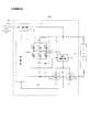
次に、電源供給回路100が動作していない状態で、バッテリBが極性を誤って逆接続された場合につき、図3を参照しながら説明する。 Next, a case where the battery B is reversely connected in reverse with the
図3のように、電源供給回路100に対してバッテリBの正極と負極が逆に接続されると、FET42のダイオードD2は、バッテリBに対して逆方向となる。一方、FET41のダイオードD1は、バッテリBに対して順方向となる。また、インバータ回路3の各スイッチング素子Q1〜Q6に並列接続された寄生ダイオードも、バッテリBに対して順方向となる。その結果、点線で示したように、逆接続されたバッテリBの正極から、インバータ回路3のスイッチング素子Q1〜Q6の寄生ダイオードと、FET41のダイオードD1を経由して、バッテリBの負極へ向う電流経路Xは、FET42のダイオードD2により遮断される。また、逆接続されたバッテリBの正極から、制御部1と電源回路2を経由して、バッテリBの負極へ向う電流経路Yも、FET42のダイオードD2により遮断される。 As shown in FIG. 3, when the positive electrode and the negative electrode of the battery B are connected in reverse to the
以上のようにして、バッテリBが逆接続された場合でも、FET42のダイオードD2によって、インバータ回路3を含むパワー系回路に大電流が流れるのを阻止することができる。また、同じダイオードD2によって、制御部1を含む信号系回路に大電流が流れるのを阻止することもできる。 As described above, even when the battery B is reversely connected, the diode D2 of the
ここで、図1と図7とを比べてみると、図7では、電源ラインL3の一端が、バッテリBの正極とFET42との接続点Pに接続されているのに対し、図1では、電源ラインL3の一端が、FET41とFET42との接続点Paに接続されている。つまり、図7の場合は、電源ラインL3が直接バッテリBの正極に接続されるのに対し、図1の場合は、電源ラインL3がFET42を介してバッテリBの正極に接続される。 Here, comparing FIG. 1 with FIG. 7, in FIG. 7, one end of the power supply line L3 is connected to the connection point P between the positive electrode of the battery B and the
このように、電源ラインL3の接続点を変えるだけで、1つのダイオードD2によって、パワー系と信号系の2系統の回路を大電流から保護することができる。このため、図7のダイオード6が不要となって、逆接続保護用の素子の数が低減する。また、電源ラインL3にダイオードによる順方向電圧降下が発生しないので、バッテリBから電源回路2を介して制御部1へ供給される電圧の減少を抑制することができる。なお、電源供給回路100の動作中は、FET42がオン状態となり、バッテリBの電圧は、FET42のダイオードD2ではなく、FET42のソースs・ドレインd間を経由して、電源ラインL3から電源回路2へ供給される。そして、FETのオン時のソース・ドレイン間の電圧降下(たとえば0.1V)は、ダイオードの順方向電圧降下(たとえば0.8V)に比べて十分小さいので、制御部1への供給電圧の減少には殆ど影響しない。 In this way, by simply changing the connection point of the power supply line L3, the two circuits of the power system and the signal system can be protected from a large current by the single diode D2. For this reason, the
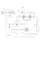
図4は、本発明の他の実施形態に係る電源供給回路200を示している。図1の電源供給回路100では、FET41とFET42が、バッテリBの正極側の電源ラインL1(第1電源ライン)上に設けられていた。これに対し、図4の電源供給回路200では、FET71とFET72が、バッテリBの負極側の電源ラインL2(第2電源ライン)上に設けられている。そして、電源ラインL4(第4電源ライン)が、FET72を介して、バッテリBの負極に接続されている。 FIG. 4 shows a
FET71(第1スイッチング素子)は、バッテリBからインバータ回路3への通電・非通電を切り替える電路開閉用のスイッチング素子である。FET72(第2スイッチング素子)は、バッテリBの逆接続時に、制御部1やインバータ回路3等を保護する保護用のスイッチング素子である。これらのFET71、72は、Nチャンネル型のMOSFETからなる。 The FET 71 (first switching element) is an electric circuit switching element that switches between energization / non-energization from the battery B to the
FET71は、FET72よりもインバータ回路3側に設けられている。FET72は、FET71とバッテリBの負極との間にあって、FET71と直列に接続されている。FET71のドレインdは、インバータ回路3の他端に接続されており、FET71のソースsは、FET72のソースsと接続されている。FET72のドレインdは、バッテリBの負極に接続されている。FET71、72の各ゲートgは、FET駆動回路5に接続されている。 The
FET71には、バッテリBに対して逆方向となるようにダイオードD3(第1ダイオード)が並列に接続されている。このダイオードD3は、FET71のソースs・ドレインd間に備わる寄生ダイオードである。FET72には、バッテリBに対して順方向となるようにダイオードD4(第2ダイオード)が並列に接続されている。このダイオードD4は、FET72のソースs・ドレインd間に備わる寄生ダイオードである。 A diode D3 (first diode) is connected in parallel to the
電源ラインL3の一端は、バッテリBの正極に接続されており、電源ラインL3の他端は、電源回路2を介して制御部1と接続されている。電源ラインL4の一端は、FET71とFET72との接続点Pbに接続されていて、FET72を介してバッテリBの負極に接続されている。電源ラインL4の他端は、制御部1と接続されている。 One end of the power supply line L3 is connected to the positive electrode of the battery B, and the other end of the power supply line L3 is connected to the
その他の構成に関しては、図1の電源供給回路100と同じであるので、図1と重複する構成についての説明は省略する。 Since the other configuration is the same as that of the
上述した電源供給回路200において、バッテリBが正常に接続された場合は、インバータ回路3の動作によって、図5に点線で示すような電流経路が形成され、インバータ回路3からモータに電流が流れて(電流経路は省略)、モータが駆動される。 In the
一方、図6に示したように、電源供給回路200が動作していない状態で、バッテリBが逆接続された場合は、FET72のダイオードD4が、バッテリBに対して逆方向となる。このため、逆接続されたバッテリBの正極から、インバータ回路3を経由してバッテリBの負極へ向う電流経路と、制御部1および電源回路2を経由してバッテリBの負極へ向う電流経路は、いずれも、点線で示したように、FET72のダイオードD4で遮断される。 On the other hand, as shown in FIG. 6, when the battery B is reversely connected while the
このようにして、本実施形態の電源供給回路200においても、バッテリBの逆接続時に、FET72のダイオードD4によって、インバータ回路3を含むパワー系回路に大電流が流れるのを阻止することができる。また、同じダイオードD4によって、制御部1を含む信号系回路に大電流が流れるのを阻止することもできる。その結果、図7のダイオード6が不要となって、逆接続保護用の素子の数を低減でき、また、バッテリBから電源回路2を介して制御部1へ供給される電圧の減少を抑制することができる。 Thus, also in the
本発明では、上述した実施形態以外にも、以下のような種々の実施形態を採用することができる。 In the present invention, the following various embodiments can be adopted in addition to the above-described embodiments.
上記実施形態では、FET41、42、71、72として、Nチャンネル型のMOSFETを用いたが、これに代えてPチャンネル型のMOSFETを用いてもよい。 In the above embodiment, N-channel type MOSFETs are used as the
上記実施形態では、スイッチング素子として、寄生ダイオードを有するFETを用いたが、FETの代わりにトランジスタを用い、回路素子としてのダイオードをトランジスタに並列接続してもよい。また、FETやトランジスタ以外のスイッチング素子を用いてもよい。 In the above embodiment, an FET having a parasitic diode is used as the switching element. However, a transistor may be used instead of the FET, and a diode as a circuit element may be connected in parallel to the transistor. Further, switching elements other than FETs and transistors may be used.
上記実施形態では、バッテリBの電圧を電源回路2で降圧して、制御部1へ供給したが、バッテリBの電圧を降圧する必要がない場合は、電源回路2を省略することができる。この場合は、電源回路2の代わりに、イグニッションスイッチIGの出力信号によりオン・オフする開閉器を設ければよい。 In the above embodiment, the voltage of the battery B is stepped down by the
上記実施形態では、バッテリBの負荷としてインバータ回路3を例に挙げたが、バッテリBの負荷は、ECU(電子制御ユニット)や車載機器などであってもよい。また、負荷は、電源供給回路100、200の外部に設けられていてもよい。 In the above embodiment, the
上記実施形態では、FET駆動回路5が制御部1とは別に設けられているが、FET駆動回路5を制御部1の内部に設けてもよい。 In the above embodiment, the
上記実施形態では、直流電源として電池(バッテリB)を例に挙げたが、直流電源は、電池に限らず、交流を直流に変換する回路から構成されていてもよい。 In the above embodiment, the battery (battery B) is taken as an example of the direct-current power supply. However, the direct-current power supply is not limited to the battery, and may be composed of a circuit that converts alternating current into direct current.
上記実施形態では、車両に搭載される電源供給回路を例に挙げたが、本発明は、車両以外の用途にも適用することができる。 In the above embodiment, the power supply circuit mounted on the vehicle is taken as an example, but the present invention can also be applied to uses other than the vehicle.
1 制御部
2 電源回路
3 インバータ回路(負荷)
5 FET駆動回路
41、71 FET(第1スイッチング素子)
42、72 FET(第2スイッチング素子)
100、200 電源供給回路
B バッテリ(直流電源)
D1、D3 ダイオード(第1ダイオード)
D2、D4 ダイオード(第2ダイオード)
L1 電源ライン(第1電源ライン)
L2 電源ライン(第2電源ライン)
L3 電源ライン(第3電源ライン)
L4 電源ライン(第4電源ライン)1
5
42, 72 FET (second switching element)
100, 200 Power supply circuit B Battery (DC power supply)
D1, D3 Diode (first diode)
D2, D4 diode (second diode)
L1 power line (first power line)
L2 power line (second power line)
L3 power line (third power line)
L4 power line (4th power line)
Claims (5)
Translated fromJapanese前記直流電源の負極と前記負荷との間に設けられる第2電源ラインと、
前記第1電源ライン上に設けられ、前記直流電源から前記負荷への通電・非通電を切り替える電路開閉用の第1スイッチング素子と、
前記第1スイッチング素子と前記直流電源の正極との間にあって、前記第1スイッチング素子と直列に接続された、逆接続保護用の第2スイッチング素子と、
前記直流電源に対して逆方向となるように、前記第1スイッチング素子に並列接続された第1ダイオードと、
前記直流電源に対して順方向となるように、前記第2スイッチング素子に並列接続された第2ダイオードと、
前記第1スイッチング素子および前記第2スイッチング素子のオン・オフを制御する制御部と、
前記直流電源の正極と前記制御部との間に設けられる第3電源ラインと、
前記直流電源の負極と前記制御部との間に設けられる第4電源ラインと、を備えた電源供給回路において、
前記第3電源ラインが、前記第2スイッチング素子を介して、前記直流電源の正極に接続されていることを特徴とする電源供給回路。A first power supply line provided between the positive electrode of the DC power supply and the load;
A second power supply line provided between the negative electrode of the DC power supply and the load;
A first switching element provided on the first power supply line for switching between energization / non-energization from the DC power supply to the load; and
A second switching element for protection against reverse connection between the first switching element and the positive electrode of the DC power supply and connected in series with the first switching element;
A first diode connected in parallel to the first switching element so as to be in a reverse direction with respect to the DC power supply;
A second diode connected in parallel to the second switching element so as to be in a forward direction with respect to the DC power supply;
A controller for controlling on / off of the first switching element and the second switching element;
A third power supply line provided between the positive electrode of the DC power supply and the control unit;
A power supply circuit comprising a fourth power supply line provided between the negative electrode of the DC power supply and the control unit;
The power supply circuit, wherein the third power supply line is connected to a positive electrode of the DC power supply via the second switching element.
前記直流電源の負極と前記負荷との間に設けられる第2電源ラインと、
前記第2電源ライン上に設けられ、前記直流電源から前記負荷への通電・非通電を切り替える電路開閉用の第1スイッチング素子と、
前記第1スイッチング素子と前記直流電源の負極との間にあって、前記第1スイッチング素子と直列に接続された、逆接続保護用の第2スイッチング素子と、
前記直流電源に対して逆方向となるように、前記第1スイッチング素子に並列接続された第1ダイオードと、
前記直流電源に対して順方向となるように、前記第2スイッチング素子に並列接続された第2ダイオードと、
前記第1スイッチング素子および前記第2スイッチング素子のオン・オフを制御する制御部と、
前記直流電源の正極と前記制御部との間に設けられる第3電源ラインと、
前記直流電源の負極と前記制御部との間に設けられる第4電源ラインと、を備えた電源供給回路において、
前記第4電源ラインが、前記第2スイッチング素子を介して、前記直流電源の負極に接続されていることを特徴とする電源供給回路。A first power supply line provided between the positive electrode of the DC power supply and the load;
A second power supply line provided between the negative electrode of the DC power supply and the load;
A first switching element that is provided on the second power supply line and that switches between energization / non-energization from the DC power supply to the load; and
A second switching element for protection against reverse connection between the first switching element and the negative electrode of the DC power supply and connected in series with the first switching element;
A first diode connected in parallel to the first switching element so as to be in a reverse direction with respect to the DC power supply;
A second diode connected in parallel to the second switching element so as to be in a forward direction with respect to the DC power supply;
A controller for controlling on / off of the first switching element and the second switching element;
A third power supply line provided between the positive electrode of the DC power supply and the control unit;
A power supply circuit comprising a fourth power supply line provided between the negative electrode of the DC power supply and the control unit;
The power supply circuit, wherein the fourth power supply line is connected to a negative electrode of the DC power supply through the second switching element.
前記第1スイッチング素子および前記第2スイッチング素子は、それぞれMOSFETからなり、
前記第1ダイオードおよび前記第2ダイオードは、それぞれ前記MOSFETのソース・ドレイン間に備わる寄生ダイオードであることを特徴とする電源供給回路。The power supply circuit according to claim 1 or 2,
The first switching element and the second switching element are each composed of a MOSFET,
The power supply circuit according to claim 1, wherein each of the first diode and the second diode is a parasitic diode provided between a source and a drain of the MOSFET.
前記第3電源ラインと前記制御部との間に、前記直流電源の電圧を降圧して前記制御部へ供給する電源回路が設けられていることを特徴とする電源供給回路。The power supply circuit according to any one of claims 1 to 3,
A power supply circuit comprising a power supply circuit for stepping down the voltage of the DC power supply and supplying the voltage to the control unit between the third power supply line and the control unit.
前記負荷が、モータ駆動用のインバータ回路であることを特徴とする電源供給回路。The power supply circuit according to any one of claims 1 to 4,
The power supply circuit, wherein the load is an inverter circuit for driving a motor.
Priority Applications (1)
| Application Number | Priority Date | Filing Date | Title |
|---|---|---|---|
| JP2014040213AJP2015165745A (en) | 2014-03-03 | 2014-03-03 | Power supply circuit |
Applications Claiming Priority (1)
| Application Number | Priority Date | Filing Date | Title |
|---|---|---|---|
| JP2014040213AJP2015165745A (en) | 2014-03-03 | 2014-03-03 | Power supply circuit |
Publications (1)
| Publication Number | Publication Date |
|---|---|
| JP2015165745Atrue JP2015165745A (en) | 2015-09-17 |
Family
ID=54188000
Family Applications (1)
| Application Number | Title | Priority Date | Filing Date |
|---|---|---|---|
| JP2014040213APendingJP2015165745A (en) | 2014-03-03 | 2014-03-03 | Power supply circuit |
Country Status (1)
| Country | Link |
|---|---|
| JP (1) | JP2015165745A (en) |
Cited By (4)
| Publication number | Priority date | Publication date | Assignee | Title |
|---|---|---|---|---|
| JP2017085761A (en)* | 2015-10-28 | 2017-05-18 | オムロンオートモーティブエレクトロニクス株式会社 | Electric motor drive circuit |
| JP2018093332A (en)* | 2016-12-01 | 2018-06-14 | 株式会社デンソー | Driver |
| KR20180127785A (en)* | 2017-05-22 | 2018-11-30 | 주식회사 만도 | Reverse Voltage Protection Circuit |
| CN112467868A (en)* | 2020-12-03 | 2021-03-09 | 芜湖华沅微电子有限公司 | Multi-power supply switching circuit and method |
Citations (5)
| Publication number | Priority date | Publication date | Assignee | Title |
|---|---|---|---|---|
| JPH0265625A (en)* | 1988-07-05 | 1990-03-06 | Sgs Thomson Microelettronica Spa | Electronic circuits protected against power battery polarity reversal |
| US6154081A (en)* | 1999-06-15 | 2000-11-28 | Delphi Technologies, Inc. | Load circuit having extended reverse voltage protection |
| JP2002095159A (en)* | 2000-09-13 | 2002-03-29 | Keihin Corp | Protection circuit |
| JP2002528938A (en)* | 1998-10-20 | 2002-09-03 | ローベルト ボツシユ ゲゼルシヤフト ミツト ベシユレンクテル ハフツング | Incorrect polarity protection circuit for a power output stage having at least one high side semiconductor switch |
| JP2010114957A (en)* | 2008-11-04 | 2010-05-20 | Jtekt Corp | Motor drive circuit and electric power steering apparatus |
- 2014
- 2014-03-03JPJP2014040213Apatent/JP2015165745A/enactivePending
Patent Citations (5)
| Publication number | Priority date | Publication date | Assignee | Title |
|---|---|---|---|---|
| JPH0265625A (en)* | 1988-07-05 | 1990-03-06 | Sgs Thomson Microelettronica Spa | Electronic circuits protected against power battery polarity reversal |
| JP2002528938A (en)* | 1998-10-20 | 2002-09-03 | ローベルト ボツシユ ゲゼルシヤフト ミツト ベシユレンクテル ハフツング | Incorrect polarity protection circuit for a power output stage having at least one high side semiconductor switch |
| US6154081A (en)* | 1999-06-15 | 2000-11-28 | Delphi Technologies, Inc. | Load circuit having extended reverse voltage protection |
| JP2002095159A (en)* | 2000-09-13 | 2002-03-29 | Keihin Corp | Protection circuit |
| JP2010114957A (en)* | 2008-11-04 | 2010-05-20 | Jtekt Corp | Motor drive circuit and electric power steering apparatus |
Cited By (6)
| Publication number | Priority date | Publication date | Assignee | Title |
|---|---|---|---|---|
| JP2017085761A (en)* | 2015-10-28 | 2017-05-18 | オムロンオートモーティブエレクトロニクス株式会社 | Electric motor drive circuit |
| JP2018093332A (en)* | 2016-12-01 | 2018-06-14 | 株式会社デンソー | Driver |
| KR20180127785A (en)* | 2017-05-22 | 2018-11-30 | 주식회사 만도 | Reverse Voltage Protection Circuit |
| KR102380893B1 (en)* | 2017-05-22 | 2022-04-01 | 주식회사 만도 | Reverse Voltage Protection Circuit |
| CN112467868A (en)* | 2020-12-03 | 2021-03-09 | 芜湖华沅微电子有限公司 | Multi-power supply switching circuit and method |
| CN112467868B (en)* | 2020-12-03 | 2024-05-31 | 芜湖华沅微电子有限公司 | Multi-path power supply switching circuit and method |
Similar Documents
| Publication | Publication Date | Title |
|---|---|---|
| JP5743934B2 (en) | Inverter device and power steering device | |
| US9564485B2 (en) | Switch driving circuit, inverter apparatus and power steering apparatus | |
| JP6867780B2 (en) | Semiconductor switch controller | |
| KR101704112B1 (en) | Motor drive device | |
| JP2015171305A (en) | power supply circuit | |
| JP5744144B2 (en) | Inductive load power supply control device | |
| JP2015008611A (en) | Dc-dc converter | |
| US20080247108A1 (en) | Load drive device | |
| JP6361531B2 (en) | Semiconductor device and motor control device | |
| JP5611420B1 (en) | DC-DC converter | |
| JP2015165745A (en) | Power supply circuit | |
| WO2018142829A1 (en) | Motor drive device and electric power steering device | |
| JP2008276727A (en) | Load drive system | |
| CN104641440A (en) | Switching method and device thereof | |
| JP2007019812A (en) | Load drive device with power supply reverse connection protection function | |
| JP6400186B2 (en) | Electric power steering device | |
| JP2003047287A (en) | Protection circuit | |
| KR20200077009A (en) | Driving circuit for motor of electric power steering apparatus | |
| WO2023026943A1 (en) | Power supply device |
Legal Events
| Date | Code | Title | Description |
|---|---|---|---|
| A621 | Written request for application examination | Free format text:JAPANESE INTERMEDIATE CODE: A621 Effective date:20160715 | |
| A977 | Report on retrieval | Free format text:JAPANESE INTERMEDIATE CODE: A971007 Effective date:20170214 | |
| A131 | Notification of reasons for refusal | Free format text:JAPANESE INTERMEDIATE CODE: A131 Effective date:20170221 | |
| A02 | Decision of refusal | Free format text:JAPANESE INTERMEDIATE CODE: A02 Effective date:20170905 |