JP2015164090A - multiple independent serial link memory - Google Patents
multiple independent serial link memoryDownload PDFInfo
- Publication number
- JP2015164090A JP2015164090AJP2015097836AJP2015097836AJP2015164090AJP 2015164090 AJP2015164090 AJP 2015164090AJP 2015097836 AJP2015097836 AJP 2015097836AJP 2015097836 AJP2015097836 AJP 2015097836AJP 2015164090 AJP2015164090 AJP 2015164090A
- Authority
- JP
- Japan
- Prior art keywords
- data
- memory
- command
- serial
- bank
- Prior art date
- Legal status (The legal status is an assumption and is not a legal conclusion. Google has not performed a legal analysis and makes no representation as to the accuracy of the status listed.)
- Pending
Links
Images


Classifications
- G—PHYSICS
- G06—COMPUTING OR CALCULATING; COUNTING
- G06F—ELECTRIC DIGITAL DATA PROCESSING
- G06F3/00—Input arrangements for transferring data to be processed into a form capable of being handled by the computer; Output arrangements for transferring data from processing unit to output unit, e.g. interface arrangements
- G06F3/06—Digital input from, or digital output to, record carriers, e.g. RAID, emulated record carriers or networked record carriers
- G06F3/0601—Interfaces specially adapted for storage systems
- G06F3/0602—Interfaces specially adapted for storage systems specifically adapted to achieve a particular effect
- G06F3/061—Improving I/O performance
- G06F3/0611—Improving I/O performance in relation to response time
- G—PHYSICS
- G11—INFORMATION STORAGE
- G11C—STATIC STORES
- G11C16/00—Erasable programmable read-only memories
- G—PHYSICS
- G06—COMPUTING OR CALCULATING; COUNTING
- G06F—ELECTRIC DIGITAL DATA PROCESSING
- G06F13/00—Interconnection of, or transfer of information or other signals between, memories, input/output devices or central processing units
- G06F13/38—Information transfer, e.g. on bus
- G06F13/42—Bus transfer protocol, e.g. handshake; Synchronisation
- G06F13/4204—Bus transfer protocol, e.g. handshake; Synchronisation on a parallel bus
- G06F13/4234—Bus transfer protocol, e.g. handshake; Synchronisation on a parallel bus being a memory bus
- G06F13/4243—Bus transfer protocol, e.g. handshake; Synchronisation on a parallel bus being a memory bus with synchronous protocol
- G—PHYSICS
- G06—COMPUTING OR CALCULATING; COUNTING
- G06F—ELECTRIC DIGITAL DATA PROCESSING
- G06F3/00—Input arrangements for transferring data to be processed into a form capable of being handled by the computer; Output arrangements for transferring data from processing unit to output unit, e.g. interface arrangements
- G06F3/06—Digital input from, or digital output to, record carriers, e.g. RAID, emulated record carriers or networked record carriers
- G06F3/0601—Interfaces specially adapted for storage systems
- G06F3/0628—Interfaces specially adapted for storage systems making use of a particular technique
- G06F3/0655—Vertical data movement, i.e. input-output transfer; data movement between one or more hosts and one or more storage devices
- G—PHYSICS
- G06—COMPUTING OR CALCULATING; COUNTING
- G06F—ELECTRIC DIGITAL DATA PROCESSING
- G06F3/00—Input arrangements for transferring data to be processed into a form capable of being handled by the computer; Output arrangements for transferring data from processing unit to output unit, e.g. interface arrangements
- G06F3/06—Digital input from, or digital output to, record carriers, e.g. RAID, emulated record carriers or networked record carriers
- G06F3/0601—Interfaces specially adapted for storage systems
- G06F3/0668—Interfaces specially adapted for storage systems adopting a particular infrastructure
- G06F3/0671—In-line storage system
- G06F3/0683—Plurality of storage devices
- G06F3/0688—Non-volatile semiconductor memory arrays
- G—PHYSICS
- G11—INFORMATION STORAGE
- G11C—STATIC STORES
- G11C16/00—Erasable programmable read-only memories
- G11C16/02—Erasable programmable read-only memories electrically programmable
- G11C16/06—Auxiliary circuits, e.g. for writing into memory
- G—PHYSICS
- G11—INFORMATION STORAGE
- G11C—STATIC STORES
- G11C16/00—Erasable programmable read-only memories
- G11C16/02—Erasable programmable read-only memories electrically programmable
- G11C16/06—Auxiliary circuits, e.g. for writing into memory
- G11C16/08—Address circuits; Decoders; Word-line control circuits
- G—PHYSICS
- G11—INFORMATION STORAGE
- G11C—STATIC STORES
- G11C16/00—Erasable programmable read-only memories
- G11C16/02—Erasable programmable read-only memories electrically programmable
- G11C16/06—Auxiliary circuits, e.g. for writing into memory
- G11C16/10—Programming or data input circuits
- G—PHYSICS
- G11—INFORMATION STORAGE
- G11C—STATIC STORES
- G11C16/00—Erasable programmable read-only memories
- G11C16/02—Erasable programmable read-only memories electrically programmable
- G11C16/06—Auxiliary circuits, e.g. for writing into memory
- G11C16/10—Programming or data input circuits
- G11C16/14—Circuits for erasing electrically, e.g. erase voltage switching circuits
- G11C16/16—Circuits for erasing electrically, e.g. erase voltage switching circuits for erasing blocks, e.g. arrays, words, groups
- G—PHYSICS
- G11—INFORMATION STORAGE
- G11C—STATIC STORES
- G11C16/00—Erasable programmable read-only memories
- G11C16/02—Erasable programmable read-only memories electrically programmable
- G11C16/06—Auxiliary circuits, e.g. for writing into memory
- G11C16/26—Sensing or reading circuits; Data output circuits
- G—PHYSICS
- G11—INFORMATION STORAGE
- G11C—STATIC STORES
- G11C16/00—Erasable programmable read-only memories
- G11C16/02—Erasable programmable read-only memories electrically programmable
- G11C16/06—Auxiliary circuits, e.g. for writing into memory
- G11C16/34—Determination of programming status, e.g. threshold voltage, overprogramming or underprogramming, retention
- G11C16/3436—Arrangements for verifying correct programming or erasure
- G11C16/3454—Arrangements for verifying correct programming or for detecting overprogrammed cells
- G11C16/3459—Circuits or methods to verify correct programming of nonvolatile memory cells
- G—PHYSICS
- G11—INFORMATION STORAGE
- G11C—STATIC STORES
- G11C5/00—Details of stores covered by group G11C11/00
- G11C5/06—Arrangements for interconnecting storage elements electrically, e.g. by wiring
- G11C5/066—Means for reducing external access-lines for a semiconductor memory clip, e.g. by multiplexing at least address and data signals
- G—PHYSICS
- G11—INFORMATION STORAGE
- G11C—STATIC STORES
- G11C7/00—Arrangements for writing information into, or reading information out from, a digital store
- G11C7/10—Input/output [I/O] data interface arrangements, e.g. I/O data control circuits, I/O data buffers
- G11C7/1015—Read-write modes for single port memories, i.e. having either a random port or a serial port
- G11C7/1018—Serial bit line access mode, e.g. using bit line address shift registers, bit line address counters, bit line burst counters
- G11C7/1021—Page serial bit line access mode, i.e. using an enabled row address stroke pulse with its associated word line address and a sequence of enabled column address stroke pulses each with its associated bit line address
- G—PHYSICS
- G11—INFORMATION STORAGE
- G11C—STATIC STORES
- G11C7/00—Arrangements for writing information into, or reading information out from, a digital store
- G11C7/10—Input/output [I/O] data interface arrangements, e.g. I/O data control circuits, I/O data buffers
- G11C7/1051—Data output circuits, e.g. read-out amplifiers, data output buffers, data output registers, data output level conversion circuits
- G—PHYSICS
- G11—INFORMATION STORAGE
- G11C—STATIC STORES
- G11C7/00—Arrangements for writing information into, or reading information out from, a digital store
- G11C7/10—Input/output [I/O] data interface arrangements, e.g. I/O data control circuits, I/O data buffers
- G11C7/1078—Data input circuits, e.g. write amplifiers, data input buffers, data input registers, data input level conversion circuits
- G—PHYSICS
- G11—INFORMATION STORAGE
- G11C—STATIC STORES
- G11C8/00—Arrangements for selecting an address in a digital store
- G11C8/10—Decoders
- G—PHYSICS
- G11—INFORMATION STORAGE
- G11C—STATIC STORES
- G11C8/00—Arrangements for selecting an address in a digital store
- G11C8/12—Group selection circuits, e.g. for memory block selection, chip selection, array selection
- G—PHYSICS
- G11—INFORMATION STORAGE
- G11C—STATIC STORES
- G11C2207/00—Indexing scheme relating to arrangements for writing information into, or reading information out from, a digital store
- G11C2207/10—Aspects relating to interfaces of memory device to external buses
- G11C2207/107—Serial-parallel conversion of data or prefetch
- G—PHYSICS
- G11—INFORMATION STORAGE
- G11C—STATIC STORES
- G11C2216/00—Indexing scheme relating to G11C16/00 and subgroups, for features not directly covered by these groups
- G11C2216/12—Reading and writing aspects of erasable programmable read-only memories
- G11C2216/30—Reduction of number of input/output pins by using a serial interface to transmit or receive addresses or data, i.e. serial access memory
Landscapes
- Engineering & Computer Science (AREA)
- Theoretical Computer Science (AREA)
- Physics & Mathematics (AREA)
- General Engineering & Computer Science (AREA)
- General Physics & Mathematics (AREA)
- Human Computer Interaction (AREA)
- Microelectronics & Electronic Packaging (AREA)
- Read Only Memory (AREA)
- Dram (AREA)
- Information Transfer Systems (AREA)
Abstract
Description
Translated fromJapanese本発明は、半導体メモリ装置に関する。より詳細には、本発明は、半導体フラッシュメモリ装置の速度および/または容量を向上させるメモリアーキテクチャに関する。 The present invention relates to a semiconductor memory device. More particularly, the present invention relates to a memory architecture that improves the speed and / or capacity of a semiconductor flash memory device.
デジタルカメラ、携帯用デジタルアシスタント、携帯用オーディオ/ビデオプレイヤ、および携帯端末などの携帯電子装置は、大容量メモリ、好ましくは、容量および速度機能が常に増加している不揮発性メモリを引き続き必要とする。例えば、現在入手可能なオーディオプレイヤは、オーディオ/ビデオデータを格納するための256メガバイトから40ギガバイトの間のメモリを有することができる。データが電力無しで維持され、したがって、電池寿命が延びるため、フラッシュメモリなどの不揮発性メモリやハードウェア装置などが好ましい。 Portable electronic devices such as digital cameras, portable digital assistants, portable audio / video players, and portable terminals continue to require large amounts of memory, preferably non-volatile memory with constantly increasing capacity and speed capabilities . For example, currently available audio players can have between 256 megabytes and 40 gigabytes of memory for storing audio / video data. Non-volatile memory such as flash memory, hardware devices, etc. are preferred because data is maintained without power and thus extends battery life.
現在、ハードディスクドライブは、高密度を有し、20から40ギガバイトのデータを格納することができるが、相対的に大きくて扱いにくい。しかし、ソリッドステートドライブとしても知られるフラッシュメモリは、密度が高く、不揮発性であり、ハードディスクドライブに比べてサイズが小さいために人気である。フラッシュメモリ技術は、EPROM技術およびEEPROM技術に基づく。各バイトが個々に消去されていたEEPROMと区別して、多数のメモリセルを一度に消去できるので、「フラッシュ」という用語が選択された。マルチレベルセル(MLC)の出現は、シングルレベルセルに比べてフラッシュメモリの密度をさらに増加させる。フラッシュメモリをNOR型フラッシュまたはNAND型フラッシュとして構成でき、NAND型フラッシュは、そのよりコンパクトなメモリアレイ構成のために、一定の面積当たりより高い密度を有することを当業者は理解されよう。さらに説明する上で、フラッシュメモリへの言及は、NOR型またはNAND型のいずれか、または他のタイプのフラッシュメモリであるものと理解されたい。 Currently, hard disk drives have high density and can store 20-40 gigabytes of data, but are relatively large and unwieldy. However, flash memory, also known as solid state drive, is popular because it is dense, non-volatile, and small in size compared to hard disk drives. Flash memory technology is based on EPROM technology and EEPROM technology. The term “flash” was chosen because many memory cells could be erased at once, distinguishing it from an EEPROM where each byte was individually erased. The advent of multi-level cells (MLC) further increases the density of flash memory compared to single level cells. Those skilled in the art will appreciate that flash memory can be configured as NOR flash or NAND flash, and NAND flash has a higher density per area due to its more compact memory array configuration. For further explanation, it should be understood that references to flash memory are either NOR-type or NAND-type, or other types of flash memory.
既存のフラッシュメモリモジュールは、現在の多くの消費者用電子装置に十分な速度で動作するが、こうしたメモリモジュールは、高いデータレートが望まれるそれ以上の装置での使用に適さないようである。例えば、高解像度の動画を記録するモバイルマルチメディア装置は、少なくとも10 MB/s のプログラミングスループットを有するメモリモジュールを必要とする可能性が高く、これは、7 MB/s の一般のプログラミングデータレートの現在のフラッシュメモリ技術では取得できない。マルチレベルセルフラッシュは、セルのプログラミングに多段階のプログラミングシーケンスが必要であるために、1.5 MB/s のかなり遅いレートを有する。 Existing flash memory modules operate at speeds sufficient for many current consumer electronic devices, but such memory modules appear to be unsuitable for use in further devices where high data rates are desired. For example, mobile multimedia devices that record high-resolution videos are likely to require memory modules with a programming throughput of at least 10 MB / s, which is a typical programming data rate of 7 MB / s. It cannot be obtained with current flash memory technology. Multi-level cell flash has a fairly slow rate of 1.5 MB / s because of the multi-step programming sequence required for cell programming.
フラッシュメモリのプログラミングおよび読み取りスループットは、フラッシュメモリの動作周波数を増加させることによって直接増加され得る。例えば、約20〜30 MHz の現在の動作周波数は、約200 MHz までひと桁増加され得る。この解決策は、簡単であるように思われるが、こうした高い周波数での信号の質に重大な問題があり、フラッシュメモリの動作周波数に実際的な制限を設ける。特に、フラッシュメモリは、所望の構成に応じて、コマンド指示を受信し、入力データを受信し、出力データを提供する、8個または16個に達する1組の並列入力/出力(I/O)ピンを使用して、他の構成要素と通信する。これは、一般に、パラレルインターフェイスとして知られている。高速動作は、例えば、信号の質を低下させるクロストーク、信号スキュー、信号減衰(signal attenuation)など、よく知られている通信を低下させる影響をもたらす。 Flash memory programming and read throughput can be directly increased by increasing the operating frequency of the flash memory. For example, the current operating frequency of about 20-30 MHz can be increased by an order of magnitude to about 200 MHz. While this solution seems simple, there are significant problems with signal quality at these high frequencies, which put practical limits on the operating frequency of flash memory. In particular, the flash memory receives a command indication, receives input data and provides output data, depending on the desired configuration, a set of 8 or 16 parallel input / output (I / O) Pins are used to communicate with other components. This is commonly known as a parallel interface. High-speed operation has the effect of reducing well-known communications, such as crosstalk, signal skew, signal attenuation, etc., which degrade signal quality.
こうしたパラレルインターフェイスは、多数のピンを使用して、データを読み取り、書き込む。入力ピンおよびワイヤの数が増えるにつれて、いくつかの望ましくない影響も増える。これらの影響には、符号間干渉、信号スキュー、およびクロストークなどがある。符号間干渉は、ワイヤに沿って移動する信号の減衰、および複数の要素がワイヤに接続されたときに引き起こされる反射から生じる。信号スキューは、複数の信号が、異なる長さおよび/または特徴のワイヤに沿って移動し、異なる時に1つの終点に到着するときに起こる。クロストークは、近接したワイヤ上での信号の不要な結合を指す。クロストークは、メモリ装置の動作速度が増すにつれて一層の問題となる。 Such a parallel interface uses a large number of pins to read and write data. As the number of input pins and wires increases, some undesirable effects also increase. These effects include intersymbol interference, signal skew, and crosstalk. Intersymbol interference results from attenuation of the signal moving along the wire and reflections caused when multiple elements are connected to the wire. Signal skew occurs when multiple signals travel along wires of different lengths and / or features and arrive at one endpoint at different times. Crosstalk refers to unwanted coupling of signals on adjacent wires. Crosstalk becomes more problematic as the operating speed of the memory device increases.
したがって、当分野では、携帯電子装置で使用するためのメモリモジュール、およびメモリモジュールへのアクセスに必要とされる入力ピンおよびワイヤの数を最低限に抑えながら、メモリ容量および/または動作速度が増加されるソリッドステートドライブアプリケーションの必要がある。 Thus, the field increases memory capacity and / or operating speed while minimizing the number of memory modules for use in portable electronic devices and the input pins and wires required to access the memory modules. There is a need for a solid state drive application.
本発明の様々な態様を基本的に理解できるようにするために、以下に本発明のいくつかの実施形態の簡単な概略を示している。この要約は、本発明の広範な概要を示すものではない。本発明の鍵となる、または重要な要素を識別するためのもの、または本発明の範囲を画定するためのものではない。単に、後述するより詳細な説明の前置きとして、本発明のいくつかの実施形態を簡略化した形で提示するためのものである。 In order to provide a basic understanding of the various aspects of the present invention, a brief summary of some embodiments of the invention is provided below. This summary is not an extensive overview of the invention. It is not intended to identify key or critical elements of the invention or to delineate the scope of the invention. Its sole purpose is to present some embodiments of the invention in a simplified form as a prelude to the more detailed description that is presented later.
本発明の態様によれば、複数のメモリバンクおよび複数のシリアルデータリンクインターフェイスを備える半導体メモリ装置が開示される。一例では、メモリ装置は、リンクインターフェイスとメモリバンクとの間のデータ転送を独立して制御する制御回路から成る。いくつかの例では、メモリバンクは、不揮発性メモリである。本発明の制御回路は、メモリ装置における様々なモジュールおよび他の回路と通信する。例えば、制御回路は、モジュールの多くを駆動する制御信号を生成する。 According to an aspect of the present invention, a semiconductor memory device comprising a plurality of memory banks and a plurality of serial data link interfaces is disclosed. In one example, the memory device comprises a control circuit that independently controls data transfer between the link interface and the memory bank. In some examples, the memory bank is a non-volatile memory. The control circuit of the present invention communicates with various modules and other circuits in the memory device. For example, the control circuit generates control signals that drive many of the modules.
半導体フラッシュメモリ装置で並行メモリ操作(concurrent memory operation)を実施する方法についても開示される。シリアルデータリンクインターフェイスおよびメモリバンクごとのステータスインジケータも含まれる。これらのステータスインジケータは、メモリバンクがビジーである(またはレディに戻る)とき、およびリンクインターフェイスがビジーである(またはレディに戻る)ときに更新される。さらに、仮想複数リンク機能(virtual multiple link feature)によって、ピンが低減されたメモリ装置は、従来技術の装置より大きいスループットで動作することができる。 A method for performing concurrent memory operation in a semiconductor flash memory device is also disclosed. A serial data link interface and a status indicator for each memory bank are also included. These status indicators are updated when the memory bank is busy (or returns to ready) and when the link interface is busy (or returns to ready). Furthermore, the virtual multiple link feature allows a memory device with reduced pins to operate at a greater throughput than prior art devices.
本発明によれば、カスケード接続された複数のメモリ装置を有するメモリシステムも開示される。メモリ装置は、直列に接続されてもよく、外部メモリコントローラは、データおよび制御信号をメモリシステムから受信し、そこに提供することができる。本発明の別の実施形態では、開示された方法を実施する実行可能命令は、光ディスクや磁気ディスクなど、コンピュータ可読媒体上に、制御論理またはコンピュータ可読命令として格納される。本発明のいくつかの実施形態では、各フラッシュメモリ装置は、一意の装置識別子を含み得る。装置は、シリアル入力データにおけるターゲット装置情報フィールドを構文解析して、ターゲット装置情報を装置の一意の装置識別番号と相関させて、この装置がターゲット装置であるかどうかを決定するように構成されてもよい。明細書を通じて、本発明の他の様々な態様も開示される。 In accordance with the present invention, a memory system having a plurality of cascaded memory devices is also disclosed. The memory devices may be connected in series, and an external memory controller can receive and provide data and control signals from the memory system. In another embodiment of the invention, executable instructions for performing the disclosed methods are stored as control logic or computer readable instructions on a computer readable medium, such as an optical disk or magnetic disk. In some embodiments of the invention, each flash memory device may include a unique device identifier. The device is configured to parse the target device information field in the serial input data and correlate the target device information with the device's unique device identification number to determine whether this device is the target device. Also good. Throughout the specification, various other aspects of the invention are also disclosed.
本発明は、一例として示されており、類似の参照番号が類似の要素を示す添付の図面に限定されない。 The present invention is illustrated by way of example and is not limited to the accompanying drawings in which like reference numbers indicate like elements.
少なくとも2つのメモリバンクを有する半導体メモリのシリアルデータインターフェイスが開示される。シリアルデータインターフェイスは、中央制御論理と通信する1つまたは複数のシリアルデータリンクを含み、各シリアルデータリンクは、コマンドおよびデータを逐次受信し、出力データを逐次出力することができる。各シリアルデータリンクは、データのプログラミングおよび読み取りのために、メモリ内の任意のメモリバンクにアクセスすることができる。シリアルインターフェイスの少なくとも1つの利点は、ある密度から別の密度まで同じである標準ピン配列の低ピン数の装置であり、したがって、ボードを再設計することなく、より高い密度への互換性のある将来のアップグレードが可能である。 A serial data interface for a semiconductor memory having at least two memory banks is disclosed. The serial data interface includes one or more serial data links that communicate with the central control logic, and each serial data link can receive commands and data sequentially and output output data sequentially. Each serial data link can access any memory bank in memory for programming and reading data. At least one advantage of the serial interface is a low pin count device with a standard pinout that is the same from one density to another, and is therefore compatible with higher densities without redesigning the board Future upgrades are possible.
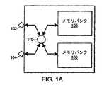
図1Aおよび図1Bは、本発明の様々な態様による、並行動作をサポートするメモリ装置例を示す高レベルの図である。図1Aは、複数のシリアルデータリンクインターフェイス102および104、および複数のメモリバンク106および108を有するメモリ装置を示す。現在示されている構成は、本明細書では、デュアルポート構成と呼ばれる。各シリアルデータリンクインターフェイスは、関連の入力/出力ピンおよびデータ入力およびデータ出力回路を有し、これについて、図2Aを参照してさらに詳しく説明する。シリアルデータリンクインターフェイスを介して転送されたデータは、逐次方式で(例えば1ビット幅ストリームのデータとして)通過する。メモリ装置内のデータリンクインターフェイス102および104のそれぞれは、独立しており、メモリバンク106および108のうちのいずれかとの間でデータ転送を行うことができる。例えば、シリアルデータリンク102は、メモリバンク106またはメモリバンク108との間でデータ転送を行うことができる。同様に、シリアルデータリンク104は、メモリバンク106およびメモリバンク108との間でデータ転送を行うことができる。示されている2つのシリアルデータリンクインターフェイスは、独立しているため、別々のメモリバンクとの間で並行してデータ転送を行うことができる。本明細書で使用される場合、リンクは、1つまたは複数のメモリバンクのパスを提供し、1つまたは複数のメモリバンクとの間のデータ転送を制御する回路を指す。制御モジュール110は、各シリアルデータリンクインターフェイス102および104と、各メモリバンク106および108との間のデータの交換を制御するためのコマンドで構成可能である。例えば、制御モジュール110は、シリアルデータリンクインターフェイス104がメモリバンク108にデータを書き込んでいるのと同じ時に、シリアルデータリンクインターフェイス102がメモリバンク106からデータを読み取ることができるように構成されてもよい。この特徴は、システム設計の柔軟性の強化、および装置の利用率(例えば、バス利用率およびコア利用率など)の強化を提供する。下記に示されるように、制御モジュール110は、制御回路、レジスタ、およびスイッチ回路を含むことができる。 1A and 1B are high-level diagrams illustrating example memory devices that support parallel operation in accordance with various aspects of the present invention. FIG. 1A shows a memory device having a plurality of serial data link interfaces 102 and 104 and a plurality of
図1Bは、単一のシリアルデータリンクインターフェイス120が制御モジュール126を介して複数のメモリバンク122および124にリンクされている一実施形態を示している。現在示されているこの構成は、本明細書では、シングルポート構成と呼ばれ、図1Aに示されているデュアルポート構成より少ないメモリ装置入力/出力ピンを使用する。制御モジュール126は、シリアルデータリンクインターフェイス120がパイプライン式にメモリバンク122および124とのデータ交換を行うことができるように、2つの操作プロセスまたはスレッドを行う、または実行するように構成されている。例えば、データがメモリバンク122に書き込まれている間、データリンクインターフェイス120は、メモリバンク124からデータを読み出すことができる。本発明の様々な態様によれば、または下記でさらに詳しく説明されるように、メモリ装置は、図1Bに示されている単一リンク構成を使用して、複数のリンク操作をエミュレートする。この単一リンクを、本明細書では仮想複数リンクとも呼ばれる複数バンク構成と共に使用することによって、他のバンクがビジー状態であり得る間、任意の使用可能なバンクへのアクセスが可能である。その結果、メモリ装置は、リンク調停回路を介して他の使用可能なバンクにアクセスすることによって、単一リンク構成の利用率の強化を達成することができる。 FIG. 1B illustrates an embodiment in which a single serial
図1Aおよび1Bに示されるメモリ装置は、単に例示の目的で、2つのメモリバンクを含む。本明細書に開示された本発明のいくつかの態様は、拡張可能であり、複数のメモリバンクおよび複数のシリアルデータリンクインターフェイスの使用を見越していることを当業者であれば理解されよう。単一メモリ装置は、例えば、2つ、4つ、またはそれ以上のメモリバンクを含むことができる。図1Cは、4つの独立したシリアルデータリンク132、134、136および138が、制御モジュール150の制御下で、4つのメモリバンク140、142、144および146とデータを交換するように構成されている一実施形態を示す。仮想複数リンク構成では、1つのリンクしか必要ないため、残りのリンク(図1Aでのデュアルリンクまたは図1Cでのクワッドリンク(quad link)ピン配列構成など)は、使用されず、NC(すなわち未接続)とみなされ得る。従来のパラレルインターフェイス構造と比較してシリアルデータリンクインターフェイスの少なくとも1つの利点は、リンクの柔軟性および大きい密度が維持されながら、メモリ装置上のピンの数が低減されることである。例えば、従来のフラッシュメモリ装置は、パッケージの複数の面にわたって48のピンを必要とし得るが、本発明の態様によるメモリ装置は、図11に示されているように、標準パッケージ1100の単一の面上のより少ないピン(例えば11ピン)の使用でよい。あるいは、必要とされる内部ボンドパッドがより少ないため、代わりに異なる小さいタイプのパッケージが使用されてもよい。 The memory device shown in FIGS. 1A and 1B includes two memory banks for illustrative purposes only. Those skilled in the art will appreciate that certain aspects of the invention disclosed herein are extensible and allow for the use of multiple memory banks and multiple serial data link interfaces. A single memory device can include, for example, two, four, or more memory banks. FIG. 1C shows that four independent
図2Aは、本発明の一実施形態による図1Aに示されているメモリ装置のより詳細な概念図を示す。メモリ装置200内の各メモリバンクのアーキテクチャは、NAND型フラッシュメモリコアアーキテクチャと同じ、または似ていてよい。図2Aは、本発明に関連する回路を示しており、図2Aを簡略化するために、いくつかの回路ブロックを意図的に省略する。例えば、フラッシュメモリコアアーキテクチャにより実装されたメモリ装置200は、メモリセルのプログラミングおよび消去に必要な高圧生成回路を含む。コアアーキテクチャ(またはコア回路)は、本発明で使用される場合、解読およびデータ転送回路など、メモリセルアレイおよび関連のアクセス回路を含む回路を指す。標準メモリアーキテクチャがよく知られているように、選択されたアーキテクチャに関連付けられているネーティブの操作もそうであり、このことを当業者は理解されたい。任意の知られている不揮発性または揮発性メモリアーキテクチャを、本発明の代替実施形態で使用できることを当業者はさらに理解されたい。 FIG. 2A shows a more detailed conceptual diagram of the memory device shown in FIG. 1A according to an embodiment of the present invention. The architecture of each memory bank in the
メモリ装置200は、メモリバンクA202およびメモリバンクB204など、それぞれのデータ、制御およびアドレス回路を含む多数の同じメモリバンク、メモリバンク202および204の両方に接続されているアドレスおよびデータパススイッチ回路206、スイッチ回路206にデータを提供し、そこからデータを受信する、各メモリバンクに関連付けられている同じインターフェイス回路205および207を含む。メモリバンク202および204は、例えばフラッシュメモリなどの不揮発性メモリが好ましい。論理的には、メモリバンク202によって受信され、提供された信号は、文字「A」で示され、メモリバンク204によって受信され、提供された信号は、文字「B」で示される。同様に、インターフェイス回路205によって受信され、提供された信号は、数字「0」で示され、インターフェイス回路207によって受信され、提供された信号は、数字「1」で示される。各インターフェイス回路205/207は、シリアルデータストリームでアクセスデータを受信し、アクセスデータは、例えばプログラミング操作のためのコマンド、アドレス情報、および入力データを含むことができる。読み取り操作では、インターフェイス回路は、読み取りコマンドおよびアドレスデータに応答して、シリアルデータストリームとして出力データを提供する。メモリ装置200は、制御インターフェイス208およびステータス/IDレジスタ回路210などのグローバル回路をさらに含み、クロック信号sclkiやresetなどのグローバル信号を、両方のメモリバンク202および204の回路およびそれぞれのインターフェイス回路205および207に提供する。以下で、上記の回路について、さらに説明する。 The
メモリバンク202は、出力データDOUT_Aを提供し、入力プログラムデータDIN_Aを受信する検出アンプおよびページバッファ回路ブロック212などのよく知られているメモリ周辺回路、および行デコーダブロック214を含む。ブロック212は列デコーダ回路も含むことを当業者であれば理解されよう。制御およびプレデコーダ回路ブロック216は、信号線ADDR_Aを介してアドレス信号および制御信号を受信し、プレデコードされたアドレス信号を行デコーダ214および検出アンプおよびページバッファ回路ブロック212に提供する。 The
メモリバンク204の周辺回路は、メモリバンク202について上述したものと同じである。メモリバンクBの回路は、出力データDOUT_Bを提供し、入力プログラムデータDIN_Bを受信する検出アンプおよびページバッファ回路ブロック218、行デコーダブロック220、および制御およびプレデコーダ回路ブロック222を含む。制御およびプレデコーダ回路ブロック222は、信号線ADDR_Bを介してアドレス信号および制御信号を受信し、プレデコードされたアドレス信号を行デコーダ220および検出アンプおよびページバッファ回路ブロック218に提供する。各メモリバンクおよびその対応する周辺回路は、よく知られているアーキテクチャで構成されてもよい。 The peripheral circuits of the memory bank 204 are the same as those described above for the
一般の操作では、各メモリバンクは、特定のコマンドおよびアドレス、および必要に応じて入力データに対応する。例えば、メモリバンク202は、読み取りコマンドおよび読み取りアドレスに応答して出力データDOUT_Aを提供し、プログラムコマンドおよびプログラムアドレスに応答して入力データをプログラムすることができる。各メモリバンクは、例えば消去コマンドなど、他のコマンドに応答することができる。 In general operation, each memory bank corresponds to a specific command and address, and input data as needed. For example, the
現在示されている実施形態では、パススイッチ206は、メモリバンク202および204と、インターフェイス回路205および207との間に信号を渡す2つのモードのうちの1つで動作することができるデュアルポート回路である。第1は、メモリバンク202およびインターフェイス回路205の信号が互いに渡される直接転送モードである。同時に、メモリバンク204およびインターフェイス回路207の信号が、直接転送モードで互いに渡される。第2は、メモリバンク202およびインターフェイス回路207の信号が互いに渡されるクロス転送モード(cross-transfer mode)である。同時に、メモリバンク204およびインターフェイス回路205の信号が互いに渡される。パススイッチ206のシングルポート構成については、下記で説明する。 In the presently shown embodiment, the path switch 206 is a dual port circuit that can operate in one of two modes of passing signals between the
上述したように、インターフェイス回路205および207は、データをシリアルデータストリームとして受信し、提供する。これは、チップのピン配列要件を低減するとともに、高動作周波数で信号スループット全体を増加させるためである。メモリバンク202および204の回路は、一般に、並列のアドレスおよびデータ用に構成されているため、変換回路が必要である。 As described above,
インターフェイス回路205は、シリアルデータリンク230、入力シリアル-パラレルレジスタブロック232、および出力パラレル-シリアルレジスタブロック234を含む。シリアルデータリンク230は、シリアル入力データSIPO、入力イネーブル信号IPEO、および出力イネーブル信号OPEOを受信し、シリアル出力データSOPO、入力イネーブルエコー信号IPEQO、および出力イネーブルエコー信号OPEQOを提供する。信号SIP0(およびSIP1)は、それぞれアドレス、コマンド、および入力データを含み得るシリアルデータストリームである。シリアルデータリンク230は、SIP0に対応するバッファードシリアル入力データ(buffered serial input data)SER_IN0を提供し、出力パラレル-シリアルレジスタブロック234からシリアル出力データSER_OUT0を受信する。入力シリアル-パラレルレジスタブロック232は、SER_IN0を受信し、それを並列の1組の信号PAR_IN0に変換する。出力パラレル-シリアルレジスタブロック234は、並列の1組の出力データPAR_OUT0を受信し、それをシリアル出力データSER_OUT0に変換し、これはその後、データストリームSOP0として提供される。出力パラレル-シリアルレジスタブロック234は、PAR_OUT0データの代わりに、そこに格納されているデータを出力するために、ステータス/IDレジスタ回路210からデータを受信することもできる。この特定の特徴のこれ以上の詳細については、後述する。さらに、シリアルデータリンク230は、別のメモリ装置200による制御信号およびデータ信号のデイジーチェーンカスケードに対応するように構成される。 The interface circuit 205 includes a
シリアルインターフェイス回路207は、インターフェイス回路205と同様に構成されており、シリアルデータリンク236、入力シリアル-パラレルレジスタブロック240、および出力パラレル-シリアルレジスタブロック238を含む。シリアルデータリンク236は、シリアル入力データSIP1、入力イネーブル信号IPE1、および出力イネーブル信号OPE1を受信し、シリアル出力データSOP1、入力イネーブルエコー信号IPEQ1、および出力イネーブルエコー信号OPEQ1を提供する。シリアルデータリンク236は、SIP1に対応するバッファードシリアル入力データSER_IN1を提供し、出力パラレル-シリアルレジスタブロック238からシリアル出力データSER_OUT1を受信する。入力シリアル-パラレルレジスタブロック240は、SER_IN1を受信し、それを並列の1組の信号PAR_IN1に変換する。出力パラレル-シリアルレジスタブロック238は、並列の1組の出力データPAR_OUT1を受信し、それをシリアル出力データSER_OUT1に変換し、これはその後、データストリームSOP1として提供される。出力パラレル-シリアルレジスタブロック238は、PAR_OUT1データの代わりに、そこに格納されているデータを出力するために、ステータス/IDレジスタ回路210からデータを受信することもできる。さらに、シリアルデータリンク230と同様に、シリアルデータリンク236は、別のメモリ装置200による制御信号およびデータ信号のデイジーチェーンカスケードに対応するように構成される。 The
制御インターフェイス208は、標準入力バッファ回路を含み、内部チップ選択信号chip_sel、内部クロック信号sclki、および内部リセット信号resetを生成し、これらはそれぞれ、CS#、SCLK、およびRST#に対応する。信号chip_selは、主にシリアルデータリンク230および236によって使用されるが、resetおよびsclkiは、メモリ装置200にわたる回路の多くによって使用される。 The
図2Bは、本発明の一実施形態によるシリアルデータリンク230の図である。シリアルデータリンク230は、入力信号OPE0、IPE0、およびSIP0を受信する入力バッファ242、信号SOP0、IPEQ0、およびOPEQ0を駆動する出力ドライバ244、信号out_en0およびin_en0をクロックアウトするフリップフロップ回路246、インバータ248およびマルチプレクサ(MUX)250を含む。信号OPE0およびSIP0の入力バッファは、chip_selに応答して使用可能にされ、信号SOP0の出力ドライバは、インバータ248による逆chip_selに応答して使用可能にされる。信号out-en0は、下記で図2Eに示される出力バッファを使用可能にし、信号SER_OUT0を提供する。信号in_en0は、入力シリアル-パラレルレジスタブロック232がSER_IN0データ、信号in_en0、out_en0、およびSER_IN0をラッチできるようにする。 FIG. 2B is a diagram of a
シリアルデータリンク230は、メモリ装置200を別のメモリ装置とデイジーチェーンカスケードできるようにする回路を含む。より詳細には、シリアル入力データストリームSIP0、およびイネーブル信号OPE0およびIPE0は、シリアルデータリンク230を介して、別のメモリ装置の対応するピンまで移動してもよい。SER_IN0は、AND倫理ゲート252によって受信され、in_en0がアクティブな高論理レベル(active high logic level)であるとき、その対応するフリップフロップ246に渡される。同時に、アクティブな高論理レベルのin_en0は、Si_next0を出力ドライバ244に渡すように、MUX250を制御する。同様に、IPE0およびOPE0は、それぞれのフリップフロップ246を介してIPEQ0およびOPEQ0にクロックアウトされ得る。シリアルデータリンク230について説明してきたが、シリアルデータリンク236は、同じ構成要素を含み、これらの構成要素は、図2Bのシリアルデータリンク230について示されているのと同じ方法で相互接続される。 The
図2Cは、入力シリアル-パラレルレジスタブロック232の図である。このブロックは、クロック信号sclki、イネーブル信号in_en0、および入力データストリームSER_IN0を受信し、SER_IN0を並列のデータ群に変換する。特に、SER_IN0は、コマンドCMD_0、列アドレスC_ADD0、行アドレスR_ADD0、および入力データDATA_IN0を提供するように変換され得る。本発明の現在開示されている実施形態は、例えば200 MHz など、高周波数で動作することが好ましい。この速度で、シリアル入力データストリームは、受信されたコマンドを解読できるより速いレートで受信され得る。シリアル入力データストリームが最初に1組のレジスタにバッファリングされるのは、このためである。現在示されている図は、信号名の指示子のみが異なる入力シリアル-パラレルレジスタブロック240にも適用されることを理解されたい。 FIG. 2C is a diagram of the input serial-
入力シリアル-パラレルレジスタブロック232は、in_en0およびsclkiを受信する入力コントローラ254、コマンドレジスタ256、一時レジスタ258、およびシリアルデータレジスタ260を含む。シリアル入力データストリームのデータ構造は予め決められているため、入力データストリームの特定の数のビットが上述したレジスタに分配され得る。例えば、あるコマンドに対応するビットがコマンドレジスタ256に格納され、行アドレスおよび列アドレスに対応するビットが一時レジスタ258に格納され、入力データに対応するビットがシリアルデータレジスタ260に格納され得る。シリアル入力データストリームのビットの分配は、入力コントローラ254によって制御されてもよく、入力コントローラは、それぞれ予め定められた数のビットが受信された後に適切なレジスタ有効化制御信号を生成するためのカウンタを含むことができる。言い換えれば、3つのレジスタのそれぞれは、シリアル入力データストリームの予め定められたデータ構造に従ってシリアル入力データストリームのデータのビットを受信し、格納するように、順次、使用可能にされ得る。 The input serial-
コマンドインタプリタ262は、コマンドレジスタ256から並行してコマンド信号を受信し、解読済みコマンドCMD_0を生成する。コマンドインタプリタ262は、受信されたコマンドを解読する、相互接続された論理ゲートまたはファームウェアで実装される標準回路である。図4に示されるように、CMD_0は、信号cmd_statusおよびcmd_idを含み得る。スイッチコントローラ264は、簡単なスイッチ回路266を制御するために、CMD_0から1つまたは複数の信号を受信する。スイッチ回路266は、一時レジスタ258に格納されているすべてのデータを並行して受信し、解読済みコマンドCMD_0に従って、列アドレスレジスタ268および行/バンクレジスタ270の一方または両方にデータをロードする。一時レジスタが常に列および行/バンクアドレスデータの両方を含んでいるわけではないので、この解読が行われることが好ましい。例えば、ブロック消去コマンドを有するシリアル入力データストリームは、行アドレスのみを使用し、この場合、一時レジスタ258に格納されている関連のビットのみが行/バンクレジスタ270にロードされる。列アドレスレジスタ268は、プログラミング操作のために、パラレル信号C_ADD0を提供し、行/バンクアドレスレジスタ270は、パラレル信号R_ADD0を提供し、データレジスタ272は、パラレル信号DATA_IN0を提供する。一括して、CMD_0、C_ADD0、R_ADD0、およびData_IN0(オプション)は、パラレル信号PAR_IN0を形成する。所望の幅は、特定の標準に準拠するようにカスタマイズまたは調整され得る設計パラメータであるため、各パラレル信号のビット幅は、指定されていない。 The
フラッシュコアアーキテクチャ実装についてのメモリ装置200の操作の一部の例が、以下の表1に示されている。表1は、CMD_0の想定されるOP(操作)コード、並びに列アドレス(C_ADD0)、行/バンクアドレス(R_ADD0)、および入力データ(DATA_IN0)の対応する状態を列挙する。 Some examples of the operation of the

さらに、表2は、入力データストリームの好ましい入力シーケンスを示している。コマンド、アドレス、およびデータが、最上位ビットから開始して、メモリ装置200に連続的にシフトインおよびシフトアウトされる。コマンドシーケンスは、1バイトコマンドコード(表2では「cmd」)で開始する。コマンドに応じて、1バイトコマンドコードの後に、コマンドアドレスバイト(表2では「ca」)、行アドレスバイト(表2では「ra」)、バンクアドレスバイト(表2では「ba」)、データバイト(表2では「data」)、および/または組合せが続くか、何も続かない場合がある。 In addition, Table 2 shows a preferred input sequence for the input data stream. Commands, addresses, and data are continuously shifted in and out of the
図2Dは、図2Aに示されているパススイッチ206の図である。スイッチ206は、論理的に2つのスイッチサブ回路274および276に分割され、これらは同様に構成される。スイッチサブ回路274は、メモリバンク202の回路に、インターフェイス回路205またはインターフェイス回路207のいずれかのコマンド、アドレス、および入力データを選択的に渡す4つの入力マルチプレクサ278を含む。これらの信号は、図2Cで一例としてPAR_IN0と予めグループ分けされている。スイッチサブ回路274は、インターフェイス回路205にメモリバンク202またはメモリバンク204のいずれかからの出力データを選択的に渡す1つの出力マルチプレクサ280を含む。スイッチサブ回路276は、メモリバンク204の回路に、インターフェイス回路205またはインターフェイス回路207のいずれかのコマンド、アドレス、および入力データを選択的に渡す4つの入力マルチプレクサ(図示せず)を含む。スイッチサブ回路276は、インターフェイス回路207にメモリバンク202またはメモリバンク204のいずれかからの出力データを選択的に渡す1つの出力マルチプレクサ(図示せず)を含む。 FIG. 2D is a diagram of the path switch 206 shown in FIG. 2A.
スイッチサブ回路274および276はいずれも、スイッチ制御信号SW_CONTの状態に応じて、直接転送モードまたはクロス転送モードで同時に動作することができる。パススイッチ回路206は、現在デュアルポート構成で示されており、これは、両方のメモリバンク202および204は、いずれかのインターフェイス回路205および207を介して同時にアクセスされ得ることを意味する。 Both of the switch sub-circuits 274 and 276 can operate simultaneously in the direct transfer mode or the cross transfer mode depending on the state of the switch control signal SW_CONT. The
本発明の別の態様によれば、図1Bで上記で例証したように、パススイッチ206は、インターフェイス回路205および207の一方のみがアクティブであるシングルポートモードで動作することができる。この構成は、未使用のインターフェイス回路に関連付けられている入力/出力パッドがもはや必要ないため、メモリ装置200のピン配列エリア要件をさらに低減することができる。シングルポート構成では、依然としてSW_CONT選択信号に応答することができるそれぞれの出力マルチプレクサ280を除いて、スイッチサブ回路274および276が直接転送モードのみで動作するように設定されている。 According to another aspect of the present invention, as illustrated above in FIG. 1B, the path switch 206 can operate in a single port mode in which only one of the
インターフェイス回路205のみがアクティブであるシングルポート実施形態では、スイッチ266およびシリアルデータレジスタ260の出力からのデータを、入力シリアル-パラレルレジスタブロック232または240のいずれかの対応する列、行/バンクおよびデータレジスタに選択的に渡す補助パススイッチ(図示せず)が入力パラレル-シリアルレジスタブロック232(またはブロック240)に含まれている。実質上、補助パススイッチは、スイッチ206と同じであり得る。したがって、両方の入力シリアル-パラレルレジスタブロック232および240の列、行/バンクおよびデータレジスタには、交互のメモリバンクアクセス、または実質的に同時のアクセスのために、データがロードされてもよい。 In a single port embodiment where only interface circuit 205 is active, the data from the output of
図2Eは、出力パラレル-シリアルレジスタブロック234の図である。出力パラレル-シリアルレジスタブロック238が同じ構成であることを理解されたい。出力パラレル-シリアルレジスタブロック234は、メモリバンクからアクセスされたデータ、または前もってレジスタに格納されているステータスデータのいずれかを提供する。より詳細には、ユーザまたはシステムは、シリアルデータリンク230または236のステータスを要求することができる。出力されたステータスデータ内の指定されたビット位置(例えばビット4)における「1」の値は、特定のシリアルデータリンクインターフェイスがビジーであることを示すことができる。固定データは、メモリ装置200の電源を投入すると、ステータスデータとともに、デフォルトの状態でプレロードすることができるチップ識別データをさらに含み得る。ステータスデータは、システムによって認識可能な事前に選択された任意のビットパターンを有するように構成され得る。図には示されていないが、図2Eは、1つまたは複数の
事前に決定された状態に基づいて、レジスタ284に格納されている1つまたは複数のビットを更新する追加の制御回路を含み得る。例えば、1つまたは複数のステータスビットは、経過したクロックサイクルの数に基づいて、またはメモリ装置200の様々な回路ブロックから受信された1つまたは複数のフラグ信号の組合せに基づいて変更され得る。FIG. 2E is a diagram of an output parallel-
出力パラレル-シリアルレジスタブロック234は、出力データPAR_OUT0をパススイッチ206から受信する第1のパラレル-シリアルレジスタ282、マルチプレクサ286から固定データを受信する第2のパラレル-シリアルレジスタ284を含む。マルチプレクサ286は、信号cmd_idに応答して、ステータスレジスタ288に格納されているステータスデータ、またはIDレジスタ290に格納されているチップ識別データのうちの一方を選択的に渡す。出力マルチプレクサ292は、ORゲート294を介して、アクティブであるcmd_idまたはcmd_statusに応答して、第1のパラレル-シリアルレジスタ282、または第2のパラレル-シリアルレジスタ284のいずれかからデータを渡す。最後に、out-en0によって使用可能にされるシリアル出力制御回路296は、SER_OUT0を提供する。 The output parallel-
ステータスインジケータのサイズおよび位置は、本発明の様々な態様に従って変更され得ることを当業者であれば理解されよう。例えば、シリアルデータリンクインターフェイスステータスインジケータは、他のタイプのステータスインジケータ(メモリバンクステータスインジケータなど)と結合されてもよく、かつ/またはレジスタブロックの外に(リンク調停モジュールや制御モジュール238などに)物理的に配置されもよい。他の例では、シリアルデータリンクインターフェイスステータスインジケータは、1ビットレジスタである。 Those skilled in the art will appreciate that the size and position of the status indicator can be varied according to various aspects of the present invention. For example, the serial data link interface status indicator may be combined with other types of status indicators (such as memory bank status indicators) and / or physically outside the register block (such as on the link arbitration module or control module 238). May be arranged. In another example, the serial data link interface status indicator is a 1-bit register.
図3A、4、5A、6A、および7は、本発明の様々な態様によるメモリ装置200によって実行されるいくつかのメモリ操作についてのタイミング図の例を示す。メモリ装置200によって実行される一部のメモリコマンドは、それだけには限定されないが、ページ読み取り、ランダムデータ読み取り、コピー用のページ読み取り、コピー用のターゲットアドレス入力、シリアルデータ入力、ランダムデータ入力、ページプログラム、ブロック消去、ステータスの読み取り、IDの読み取り、構成レジスタの書き込み、装置名エントリの書き込み、リセット、および/またはバンク選択を含む。上の図、および表1および2に示されているメモリ装置200の上述された実施形態を参照して、タイミング図についての以下の説明
を行う。3A, 4, 5A, 6A, and 7 show example timing diagrams for several memory operations performed by the
図3Aのタイミング図で示された例では、「ページ読み取り」メモリコマンド314が、本発明によるメモリ装置200のシリアルデータリンク230で受信される。さらに、図3Bは、図3Aのタイミング図における「ページ読み取り」メモリコマンド314の操作と並行する簡略化したフローチャートを示す。実際に、図3Bに示されたステップは、図3Aのタイミング図と共に説明される。一例として、ステップ324で、「ページ読み取り」メモリコマンド314は、メモリ装置200のシリアルデータリンク230で読み取られる。 In the example shown in the timing diagram of FIG. 3A, a “read page”
この例における受信データストリームは、コマンドデータ(第1バイト)、コマンドアドレスデータ(第2および第3バイト)、および行およびバンクアドレスデータ(第4、第5、および第6バイト)を含む6バイトのシリアルデータストリーム(すなわち、シリアル入力データ)である。バンクアドレスは、パススイッチ206を介したバンク202または204のいずれかへのアクセスを決定するために使用され得る。異なるメモリコマンドが異なるデータストリームを有し得ることを当業者であれば理解されよう。例えば、「ランダムデータ読み取り」メモリコマンドは、コマンドデータ(第1バイト)および列アドレスデータ(第2および第3バイト)の3バイトのみの予め定められたデータストリームを有する。後者の例では、シリアル入力データのアドレスフィールドは、列アドレスのみを含み、2バイト長であった。一方、前者の例では、アドレスフィールドは、5バイト長であった。本明細書に開示された全体の再点検の後、本発明の様々な態様に従って多数のメモリコマンドおよび予め定められたデータストリームが明らかであることを当業者であれば理解されよう。 The received data stream in this example is 6 bytes including command data (first byte), command address data (second and third bytes), and row and bank address data (fourth, fifth and sixth bytes) Serial data stream (ie, serial input data). The bank address can be used to determine access to either
引き続き図3aに示されている「ページ読み取り」メモリコマンドを伴う例で、チップ選択(CS#)信号302は、低く設定され、入力ポートイネーブル(IPEx)信号306に応答して、高く設定され、一方、シリアル入力(SIPx)ポート308は、シリアルクロック(SCLK)信号304の最初の立ち上がりエッジでサンプリングされる(xは、例えば、リンク0インターフェイス230やリンク1インターフェイス236など、リンクインターフェイス番号を表すプレースホルダーとして働く)。データ読み出し(ステップ328)は、「ページ読み取り」メモリコマンド314に対応するデータストリームである。CS#信号302は、メモリ装置200への入力であり、数ある中でも、メモリ装置200がアクティブである(例えばCS#が低いとき)かどうかを示すために使用され得る。IPEx信号306は、受信データストリームが特定のリンクインターフェイスで受信される(例えばIPExが高いとき)かどうか、または特定のリンクインターフェイスが受信データストリームを無視する(例えばIPExが低いとき)かどうかを示す。受信データストリームは、リンクインターフェイスのSIPx308でメモリ装置において受信される。最後に、システムクロック(SCLK)信号304は、メモリ装置200への入力であり、メモリ装置200の多数の回路によって実行される様々な操作を同期するために使用される。本発明の様々な態様によるメモリ装置は、こうしたクロック信号と同期され得る(例えば、操作およびデータ転送は、クロック信号の立ち上がりおよび/または立ち下がりエッジに起こる)、または非同期であり得る(例えば同期ではない)ことが当業者には明らかである。あるいは、ダブルデータレート(DDR)実装では、SCLKクロック信号の立ち上がりおよび立ち下がりエッジは、情報をラッチするために使用され得る。しかし、図3Aの例では、入力データは、SCLKの立ち下がりエッジにおいてラッチされ、出力データ322は、SCLKの立ち上がりエッジ後、シリアル出力ピン312 SOPxに現れる。 Continuing with the example with the “page read” memory command shown in FIG. 3a, the chip select (CS #) signal 302 is set low, and is set high in response to the input port enable (IPEx) signal 306, On the other hand, the serial input (SIPx)
「ページ読み取り」のステータスは、図3Aに示されているように、SOPxピン312においてチェックされ、それによって、「レディ」指示が表示される時刻318までに「バンクビジー」結果がSOPx上に提供され、時刻322間に、まもなく出力データが現れる。図3Aは、「ページ読み取り」およびその後の「ステータスの読み取り」を示しているが、本発明の態様によれば、「ステータスの読み取り」無しの「ページ読み取り」も企図される。その実施形態では、データは、レディとなるまで出力データがSOPxピン上に提供されないことになる。 The status of “page read” is checked at SOPx pin 312 as shown in Figure 3A, thereby providing a “bank busy” result on SOPx by
SIPxによってサンプリングされたコマンドデータは、図2Cで適切なレジスタ(コマンドレジスタ256など)に書き込まれる。第1バイトがコマンドデータであるような受信データストリームを設計するオプションの少なくとも1つの利点は、データが追加の処理無しにコマンドレジスタに転送され得ることである。データストリームにおけるその後のバイトは、メモリコマンドのタイプに従って、アドレスデータおよび/または入力データであり得る。本発明の様々な態様によるメモリ装置によって認識されたメモリコマンドの組は、単語ベース(すなわち16ビット)、または任意のI/O幅で定義され得ることを当業者であれば理解されよう。図3Aでは、コマンドデータ(すなわち「ページ読み取り」314に対応する00h)の後に、5バイトのアドレスデータ、すなわち2バイトの列アドレスデータ、および3バイトの行/バンクアドレスデータが続く。アドレスデータは、図2Cのアドレスレジスタ258に書き込まれる。アドレスデータは、メモリバンク202内に格納されている読み取られるべきデータを探すために使用される。このプロセスの間、プレデコーダ回路216、回路内列デコーダ(column decoder in circuit)212、および行デコーダ214は、読み取られるべきデータを選択するために使用される。例えば、プレデコーダモジュール216は、アドレス情報を事前解読するために使用される。その後、回路内列デコーダ212、および行デコーダ214は、アドレスデータに対応するビット線およびワード線を稼働させるために使用される。「ページ読み取り」コマンドの場合、ワード線に対応する複数のビット線が稼働される。その後、メモリバンク202に格納されているデータは、検出アンプによって検出された後、回路内ページレジスタ212に転送される。ページレジスタ内のデータは、図3Aの時刻318まで、すなわち出力ピンSOPxが「ビジー」を示すまで使用できない場合がある。経過した時間量は、転送時間(tR)と呼ばれる。転送期間は、時刻318(図3A)に終了し、tRの期間中続く。 Command data sampled by SIPx is written to an appropriate register (such as command register 256) in FIG. 2C. At least one advantage of designing an incoming data stream where the first byte is command data is that the data can be transferred to the command register without additional processing. Subsequent bytes in the data stream may be address data and / or input data, depending on the type of memory command. Those skilled in the art will appreciate that the set of memory commands recognized by a memory device according to various aspects of the present invention may be defined on a word basis (ie, 16 bits), or any I / O width. In FIG. 3A, command data (ie, 00h corresponding to “page read” 314) is followed by 5 bytes of address data, ie, 2 bytes of column address data, and 3 bytes of row / bank address data. The address data is written into the
転送期間が経過する前に、メモリバンクステータスインジケータは、特定のメモリバンク(例えばメモリバンク202)が「ビジー」であることを示すように設定される。図3Aのメモリバンクステータスインジケータ例は、ビットの1つ(例えばビット4)がメモリバンク202(すなわちバンク0)が「ビジー」であるか「レディ」であるかを示す1バイトフィールドである。メモリバンクステータスインジケータは、図2Eのステータスレジスタ288に格納されている。メモリバンクが受信データストリームから識別された後、メモリバンクステータスインジケータが更新される(例えばビット4が「0」に設定される)。メモリ操作が完了すると、メモリバンクがもはや「ビジー」ではない(すなわち「レディ」)ことを示すように、バンクステータスインジケータが更新される(例えばビット4が「1」に設定される)。以下でより詳しく説明するように、バンクステータスインジケータおよびSOPx出力ピンの両方が「ビジー」ステータスを示すことに留意されたい。図3Aでは、メモリバンクステータスインジケータは、1バイトフィールドとして示されているが、そのサイズは、必ずしもそのように限定されるわけではないことを当業者であれば理解されよう。大きめなステータスインジケータの少なくとも1つの利点は、多めの量のメモリバンクのステータスを監視することができることである。さらに、ステータスインジケータは、他のタイプのステータス(例えば、「ページプログラム」などのメモリ操作が行われた後、メモリバンクが「合格」ステータスであるか「不合格」ステータスであるか)を監視するために使用され得る。さらに、各ビットが異なるメモリバンクのステータスを示すように実装されるこの例のステータスインジケータが例にすぎないことは、当業者には明らかであろう。例えば、ビットの組合せの値が、(例えば、論理ゲートおよび他の回路を使用することによって)メモリバンクのステータスを示すために使用されてもよい。メモリバンクステータスインジケータに対応する「ステータスの読み取り」コマンドの操作については、図7との関連で、下記で説明される。 Before the transfer period elapses, the memory bank status indicator is set to indicate that a particular memory bank (eg, memory bank 202) is “busy”. The example memory bank status indicator of FIG. 3A is a 1 byte field where one of the bits (eg, bit 4) indicates whether the memory bank 202 (ie, bank 0) is “busy” or “ready”. The memory bank status indicator is stored in the
図3Aの例のメモリバンクステータスインジケータは、「ステータスの読み取り」メモリコマンド316を使用して読み取られる(ステップ328)。「ステータスの読み取り」コマンド316は、転送期間中のいつかに、レジスタブロック224内のコマンドレジスタに送信される。「ステータスの読み取り」コマンドは、メモリバンク202からページレジスタ216へのデータの転送がいつ完了するかを決定するために、メモリバンク202のステータスを監視するようメモリ装置200に指示する。「ステータスの読み取り」コマンドは、制御モジュール238からデータパス制御モジュール230を介して、またはデータパス制御モジュールによって直接送信される。「ステータスの読み取り」コマンドが発行される(例えば、コマンドインタプリタ228および/または制御モジュール238に送信される)と、出力ポートイネーブル(OPEx)信号310は、高く駆動され、メモリバンクステータスインジケータの内容は、シリアル出力(SOPx)ポート312を介して出力される。IPEx信号306と同様に、OPEx信号310は、高く設定されると、シリアル出力ポートバッファ(例えばデータ出力レジスタ)を使用可能にする。図3Aの時刻318で、SOPxにおけるステータスインジケータデータは、メモリバンク202が「ビジー」ステータスから「レディ」ステータスに変わった(ステップ330)ことを示す。ステータスインジケータの内容は、もはや必要ないため、OPEx信号310は、低に戻される。 The memory bank status indicator of the example of FIG. 3A is read using the “read status” memory command 316 (step 328). A “read status”
次に、図3Aで、IPEx信号が高く設定され、データレジスタから出力ピンSOPxにデータを提供するために、終了アドレスデータ(trailing address data)の無い「ページ読み取り」コマンド320が、レジスタブロック224内のコマンドレジスタに再発行される(ステップ332)。その後、OPEx信号が高く設定され(およびIPExが低に戻され)、ページレジスタ216の内容がSOPx312に転送される。出力データが、メモリ装置200からリンクインターフェイス230を介して提供される(ステップ334)。エラー訂正回路(図示せず)は、出力データをチェックし、エラーが検出された場合は、読み取られたエラーを示すことができる。ページ読み取りコマンドのステータスおよび再アサートの監視は、システムによって自動に行われ得ることを当業者であれば理解されよう。図3Aは、単に、本発明の態様によるメモリ装置操作の一例にすぎず、本発明は、そのように限定されない。例えば、本発明の様々な態様に従って、他のメモリコマンドおよびタイミング図が描かれる。 Next, in FIG. 3A, in order to provide data from the data register to the output pin SOPx with the IPEx signal set high, a “page read”
例えば、図4に、「ページ読み取り」コマンドに続く「ランダムデータ読み取り」コマンドのタイミング略図が示されている。「ランダムデータ読み取り」コマンドは、「ページ読み取り」コマンドまたは「ランダムデータ読み取り」コマンドの後の単一または複数の列アドレスにおける追加データの読み取りを可能にする。「ランダムデータ読み取り」コマンド402のデータストリームは、コマンドデータ(第1バイト)、および列アドレスデータ(第2および第3バイト)の3バイトから成る。データが「ページ読み取り」コマンドで選択された同じ行から読み取られるため、行アドレスデータは必要ない。通常の「ページ読み取り」コマンドが完了した後発行された「ランダムデータ読み取り」コマンドによって、現在のページ(すなわち、前のコマンド中に読み取られたページ)からのデータ404の一部が出力される。「ランダムデータ読み取り」コマンドの少なくとも1つの利点は、データがすでにメモリバンク202に対応する回路のページレジスタ212に存在するため、事前に選択されたページからのデータが出力され得る効率が増すことである。 For example, FIG. 4 shows a timing diagram of a “random data read” command following a “page read” command. The “Read Random Data” command allows reading of additional data at a single or multiple column addresses after a “Read Page” command or a “Read Random Data” command. The data stream of the “random data read”
図5Aについて、「ページプログラム」コマンドのタイミング図が示されている。図2Aに示された実施形態は、シリアルデータ入力および出力リンク構造を使用するため、ページをプログラムし始める前に、まず、プログラムデータがバンクページレジスタにロードされなければならない。これは、「シリアルデータ入力コマンド」で達成される。「シリアルデータ入力」コマンド502は、データのあるページまで(例えば2,2112バイト)が回路内ページバッファ212にロードされるシリアルデータロード期間から成る。データレジスタのロードのプロセスが完了した後、データをバンクレジスタから適切なメモリバンクに転送するための「ページ開始」コマンド504が発行される。コマンド504が発行されると、内部書き込みステートマシン(internal write state machine)が、適切なアルゴリズムを実行し、操作をプログラムし、確認するようタイミングを制御する。したがって、本発明の一実施形態によれば、「ページ開始」コマンドは、シリアルデータ入力および確認の2つのステップに分割される。「ページプログラム」コマンドが正常に完了すると、メモリバンクステータスインジケータは、正常な操作を示す「合格」(「不合格」ではなく)結果を提供する。他の点では、図5Aの例に関わるタイミング図およびステップは、図3Aのものと類似しており、これについては、上記でより詳しく説明している。 With respect to FIG. 5A, a timing diagram for the “page program” command is shown. Since the embodiment shown in FIG. 2A uses a serial data input and output link structure, program data must first be loaded into a bank page register before starting to program a page. This is accomplished with a “serial data input command”. The “serial data input”
さらに、図5Bは、図5Aのタイミング図における「ページプログラム」コマンドの操作と並行する簡略化したフローチャートを示す。ステップ506で、「シリアルデータ入力」コマンド502がシリアル入力ポート(SIP)ラインに入力される。この例でのSIPラインに入力されたデータストリームは、コマンドデータ(第1バイト)で始まるマルチバイトシリアルデータストリーム(すなわち、シリアル入力データ)である。次に、コマンドアドレスデータ(シリアルデータストリームの第2および第3バイト)および行アドレス/バンクデータ(シリアルデータストリームの第4、第5、および第6バイト)がSIPラインに入力される(ステップ508)。次いで、入力データは、シリアルデータストリームのその後のバイトにおいて、SIPラインに入力される(ステップ510)。ステップ512で、「プログラム開始」コマンド504が発行される。次に、操作のステータスを監視するために、「ステータスの読み取り」コマンドがSIPラインに書き込まれる(ステップ514)。これによって、メモリ装置は、メモリバンクステータスレジスタのステータスビットを監視する。メモリバンクがレディであり(ステップ516)、メモリバンクが「合格」であることを示す(ステップ518)ことをステータスビットが示すと、「ページプログラム」メモリコマンドは、正常に実行されている。 Further, FIG. 5B shows a simplified flowchart in parallel with the operation of the “page program” command in the timing diagram of FIG. 5A. In
さらに、「コピー用のページ読み取り」および「コピー用のターゲットアドレス入力」メモリコマンドは、本発明の態様によるメモリ装置によって実行される他の操作である。「コピー用のページ読み取り」コマンドがシリアルリンクインターフェイスのコマンドレジスタに書き込まれた場合、メモリ位置の内部ソースアドレス(3バイト)が書き込まれる。ソースアドレスが入力されると、メモリ装置は、指定されたソースアドレスにおけるメモリバンクの内容をデータレジスタに転送する。その後、「コピー用のターゲットアドレス入力」メモリコマンド(3バイトのバンク/行アドレスシーケンスを含む)は、ページコピー操作のターゲットメモリアドレスを指定するために使用される。次いで「ページプログラム」コマンドは、内部制御論理に、ページデータをターゲットアドレスに自動的に書き込ませるようにするために使用され得る。「ステータスの読み取り」コマンドは、その後、コマンドの正常な実行を確認するために使用されてもよい。本明細書の全開示の再点検の後、当業者には他のメモリ操作が明らかである。 Further, the “page read for copy” and “input target address for copy” memory commands are other operations performed by the memory device according to aspects of the present invention. When a “page read for copy” command is written to the command register of the serial link interface, the internal source address (3 bytes) of the memory location is written. When the source address is input, the memory device transfers the contents of the memory bank at the designated source address to the data register. The “Copy Target Address Input” memory command (including a 3-byte bank / row address sequence) is then used to specify the target memory address for the page copy operation. The “page program” command can then be used to cause the internal control logic to automatically write the page data to the target address. The “read status” command may then be used to confirm the successful execution of the command. After reviewing the entire disclosure herein, other memory operations will be apparent to those skilled in the art.
図6Aについて、「消去」(または「ブロック消去」)コマンドのタイミング図が示されている。さらに、図6Bは、図6Aのタイミング図における「消去」コマンドの操作と並行する簡略化したフローチャートを示す。消去が一般にブロックレベルで行われることを、当業者であれば認識している。例えば、フラッシュメモリ装置200は、各バンクに、ブロック当たり64の2,112バイト(2,048+64バイト)ページとして編成される2,048個の消去可能ブロックを有し得る。各ブロックは、132,000バイト(128,000+4,000バイト)である。「消去」コマンドは、一度に1つのブロックに対して働く。ブロック消去は、ステップ610で、「消去」コマンドに対応するコマンドデータ602を、ステップ612での行およびバンクアドレスの3バイトとともに、SIPxを介してコマンドレジスタに書き込むことによって開始される。コマンドおよびアドレスの入力が完了した後、内部消去ステートマシン(internal erase state machine)は、プロパティアルゴリズムを自動的に実行し、操作を消去し、確認するのに必要なすべてのタイミングを制御する。「消去」操作は、「1」の論理値をメモリのあるブロック内のすべてのメモリ位置に書き込む、またはプログラミングすることによって実行され得ることに留意されたい。tBERS(すなわちブロック消去時刻)がいつ完了するかを決定するために消去ステータスを監視するために、ステップ614で、「ステータスの読み取り」コマンド604(例えば、70hに対応するコマンドデータ)が発行され得る。「読み取りステータス」コマンドの後、新しいコマンドが与えられるまで、すべての読み取りサイクルがメモリバンクステータスレジスタから来る。この例では、メモリバンクステータスレジスタの適切なビット(例えばビット4)が、対応するメモリバンクの状態(ビジーやレディなど)を反映する。ステップ618でバンクがレディになると、ステップ620でメモリバンクステータスレジスタの適切なビット(例えばビット0)がチェックされて、ステップ622で消去操作が合格した(すなわち正常に実行された)か、ステップ624で不合格になったかを決定する。いくつかの点では、図6Aの例に関わるタイミング図およびステップは、図3Aのものと類似しており、これについては、上記でより詳しく説明している。 With respect to FIG. 6A, a timing diagram for an “erase” (or “block erase”) command is shown. Further, FIG. 6B shows a simplified flowchart in parallel with the operation of the “erase” command in the timing diagram of FIG. 6A. Those skilled in the art recognize that erasure is generally performed at the block level. For example, the
図7について、メモリバンクステータスインジケータは、「ステータスの読み取り」メモリコマンドを使用して読み取られる。702で、「ステータスの読み取り」コマンド(すなわち「70h」)が図2Cのコマンドレジスタ256に送信されると、メモリ装置200は、メモリバンク202のステータスを監視するように指示されて、数ある中でも、メモリバンク202から回路内ページバッファ212へのデータの転送がいつ正常に完了するかを決定する。「ステータスの読み取り」コマンドが発行される(例えば、コマンドインタプリタ262に送信される)と、出力ポートイネーブル(OPEx)信号は、高く駆動され、メモリバンクステータスインジケータの内容は、704で、シリアル出力(SOPx)ポートを介して出力される。OPEx信号は、高に設定されると、シリアル出力ポートバッファ(例えばデータ出力レジスタ)を使用可能にする。図7の例では、メモリバンクステータスインジケータは、1バイト(すなわち8ビット)フィールドであり、各ビットは、数ある中でも、メモリバンク(例えば、メモリバンク202)が「ビジー」であるか、「レディ」であるか、および/またはメモリバンクに対して行われる操作(例えば「消去」コマンド)が「合格」したか「不合格」であったかを示す。図7では、メモリバンクステータスインジケータは、1バイトフィールドとして示されているが、そのサイズは、必ずしもそのように限定されるわけではないことを当業者であれば理解されよう。大きめなステータスインジケータの少なくとも1つの利点は、多めの量のメモリバンクのステータスを監視することができることである。さらに、この例のステータスインジケータは、各ビットが異なるメモリバンクのステータスを示すように実装されているが、本発明はそのように限定されないことは、当業者には明らかであろう。例えば、ビットの組合せの値が、(例えば、論理ゲートおよび他の回路を使用することによって)メモリバンクのステータスを示すために使用されてもよい。 With respect to FIG. 7, the memory bank status indicator is read using the “read status” memory command. At 702, when a “read status” command (ie, “70h”) is sent to the
図8A、8B、および8Cは、2つの独立したシリアルデータリンク230および236を使用して並行操作を行うために使用される本発明の態様によるメモリ装置のタイミング図を示す。本発明の態様によるメモリ装置によって実行されるいくつかの並行操作は、それだけには限定されないが、並行読み取り、並行プログラム、並行消去、プログラム中の読み取り、消去中の読み取り、および消去中のプログラムを含む。図8Aは、バンクA(バンク202)およびバンクB(バンク204)に対して行われる並行「ページ読み取り」操作を示す。図8Aでは、バンクAは、「バンク0」として表され、バンクBは、「バンク1」として表される。本明細書の全開示の再点検の後、当業者には他の並行操作が明らかになる。 FIGS. 8A, 8B, and 8C show timing diagrams of a memory device according to an embodiment of the invention used to perform parallel operations using two independent
図8Aを参照すると、メモリ装置200内の異なるメモリバンクで指示された並行「ページ読み取り」操作802、804が実行される。2つのリンクインターフェイス230、236を含むメモリ装置200では、「ページ読み取り」802は、データリンクインターフェイス230(すなわちリンク0)を介して保留中であり、「ページ読み取り」コマンド804は、データリンクインターフェイス236(すなわちリンク1)を介して発行される。図8Aは、バンク1での「ページ読み取り」の前にバンク0での「ページ読み取り」が開始することを示しているが、2つの「ページ読み取り」操作は、実質的に同時に始まり、並行して動作することができる。「ページ読み取り」コマンドのそれぞれから出力されたデータ806、808は、それぞれのデータリンクインターフェイスを介して同時に送信される。したがって、メモリ装置200内の各データリンクインターフェイスは、メモリバンクのいずれかにアクセスし、独立して動作し得る。この特徴の少なくとも1つの利点は、システム設計における柔軟性の向上、および装置の稼働率の強化(例えば、バス稼働率やコア稼働率など)である。 Referring to FIG. 8A, concurrent “page read”
図8Aにおけるメモリバンクからデータリンクインターフェイスに出力されたデータのパスは、上述した図3Aのものに似ている。例えば、メモリバンク204から出力されたデータは、S/Aおよびページバッファ218から、例えばバンクアドレスによって制御されるパススイッチ206を通過して、出力パラレル-シリアルレジスタブロック238、およびシリアルデータリンクインターフェイス236(すなわちリンク1)に流れる。メモリバンク202および204とシリアルデータリンクインターフェイス230、236との間のそれぞれの同時のデータ転送は、互いに独立して起こる。バンクアドレスは、パススイッチ206を制御することができるため、シリアルデータリンクインターフェイス236は、代わりにバンク202にアクセスすることができる。メモリ装置200内のデータリンクインターフェイスの数は、メモリ装置200上のポートまたはピンの数に限定されない。また、メモリ装置200におけるリンクインターフェイスの数も、メモリ装置におけるメモリバンクの数によって制限されない。例えば、各データリンクインターフェイスは、単一の入力ストリームおよび/または単一の出力ストリームを処理することができる。 The path of data output from the memory bank to the data link interface in FIG. 8A is similar to that of FIG. 3A described above. For example, data output from the memory bank 204 passes from the S / A and page buffer 218 through, for example, a
さらに、本発明の態様によれば、図8Bは、メモリ装置200における異なるメモリバンクで指示された「ページ読み取り」コマンド810および「ページプログラム」コマンド812が並行して実行されるタイミング図を示している。この例では、読み取り操作(「ページ読み取り」810)がシリアルデータリンクインターフェイス230を介して複数のメモリバンクのうちの1つ(例えばメモリバンク202)で実行されている。一方、同時に、書き込み操作(「ページプログラム」812)がシリアルデータリンクインターフェイス236を介して複数のメモリバンクのうちの別のもの(例えばメモリバンク204)で実行されている。本発明の様々な態様によれば、メモリ装置200内の各リンクは、メモリバンクのいずれかにアクセスし、独立して動作することができる。 Further, according to an aspect of the present invention, FIG. 8B shows a timing diagram in which a “page read”
図8Cは、2つのシリアルデータリンクインターフェイスおよび2つのメモリバンクが並行メモリ操作を実行しているメモリ装置200のタイミング図の例である。まず、メモリバンク0(バンク202)で指示された「消去」コマンド814は、シリアルインターフェイスリンク0(シリアルデータリンク230)から発行される。リンク0(シリアルデータリンク230)およびメモリバンク0(バンク202)が「消去」コマンド814でビジーである間、「ページプログラム」コマンドがメモリ装置で受信され、リンク1(シリアルデータリンク236)を使用するように指示される。したがって、「ページプログラム」コマンド816は、シリアルデータリンクインターフェイス1(シリアルデータリンク236)からメモリバンク0(バンク202)において実行される。一方、同時に、読み取りコマンド818は、シリアルデータインターフェイス0(シリアルデータリンク230)によってメモリバンク1(バンク204)において実行される。データは、メモリコマンド814中に、シリアルデータリンクインターフェイス0(シリアルデータリンク230)とバンク0(バンク202)との間に転送され、メモリコマンド818中に、同じリンクインターフェイス0(シリアルデータリンク230)とバンク1(バンク204)との間に転送される。したがって、本発明の態様によれば、メモリ装置200における各リンクは、メモリバンク(すなわちビジーではないメモリバンク)のいずれかに、独立してアクセスする。 FIG. 8C is an example of a timing diagram for a
本明細書に開示された全体の再点検の後、図8A、8B、および8Cは、単に、本発明に従って描かれた並行メモリ操作のいくつかの例を示しているにすぎないことは、当業者には明らかであろう。並行操作の他の例は、それだけには限定されないが、並行消去、プログラム中の読み取り、消去中の読み取り、消去中のプログラム、プログラム中の消去、および/または並行プログラムを含む。フローチャートにおけるステップの順序の記述は、ステップをその特定の順序のみに限定するように解釈されるべきではないことを当業者であれば理解されよう。例えば、ステータスの読み取りコマンドの有無に関わらず、読み取りコマンドおよびプログラムコマンドを発行できる。 After the overall review disclosed herein, it should be noted that FIGS. 8A, 8B, and 8C are merely illustrative of some examples of concurrent memory operations depicted in accordance with the present invention. It will be clear to the contractor. Other examples of concurrent operations include, but are not limited to, concurrent erase, read during program, read during erase, program being erased, erase during program, and / or concurrent program. Those skilled in the art will appreciate that a description of the order of steps in a flowchart should not be construed as limiting the steps to only that particular order. For example, a read command and a program command can be issued regardless of the presence or absence of a status read command.
図9は、本発明の態様による、複数のシリアルリンクインターフェイスと複数のメモリバンクとの間の2つの並行書き込み操作のより一般的な説明を示す。図9は、本発明の一実施形態による、シリアルデータリンクインターフェイスを介してデータをメモリバンクに書き込む方法を示す。まず、ステップ902で、データストリームがシリアルデータリンクインターフェイスで受信される。データストリームは、レジスタに格納されるコマンド、アドレス、およびデータを含む。次に、ステップ904で、第1のシリアルデータリンクインターフェイスに対応するシリアルデータリンクインターフェイスステータスインジケータは、第1のシリアルデータリンクインターフェイスが使用されていることを示すように更新される。ステップ904は、ステータスレジスタ内のビット値を変更することを含む。ステップ904における更新は、特定のインターフェイスが使用されていることを示す。ステップ906で、データストリームは、第1のメモリバンク識別子を抽出するために構文解析される。メモリバンク識別子は、メモリ装置内のメモリバンクを一意に識別する。メモリバンク識別子は、データストリームのアドレスフィールドまたは他のフィールド内に含まれ得る。次に、メモリバンク識別子を抽出するためにデータストリームを構文解析した後、ステップ908で、対応するメモリバンクステータスインジケータが更新される。ステップ904および908で行われる更新は、例えば、ステータス/IDレジスタ210内の制御回路によって生成される制御信号によって駆動され得る。これらの制御信号は、簡潔にするために、含まれているタイミング図から省略されている。最後に、ステップ910で、データが第1のシリアルデータリンクと第1のメモリバンクとの間に送られる。データは、最初にメモリバンクページレジスタに書き込まれ、次いでその後、メモリバンク内にプログラムされるため、ステップ910は、この一般的な説明では簡略化されていることに留意されたい。 FIG. 9 shows a more general description of two concurrent write operations between multiple serial link interfaces and multiple memory banks, according to an aspect of the present invention. FIG. 9 illustrates a method for writing data to a memory bank via a serial data link interface according to one embodiment of the invention. First, at
一方、示されている操作902と並行して、別の書き込みデータ操作が、異なるシリアルデータリンクインターフェイスを介して、異なるメモリバンクにおいて行われる。言い換えれば、第2のメモリ操作は、第2のシリアルデータリンクインターフェイスと第2のメモリバンクとの間に送られる第2のデータストリームを使用して、並行して行われる。まず、第2のデータストリームは、ステップ912で、複数のシリアルデータリンクインターフェイスのうちの第2のもので受信される。ステップ912および902で言及されたシリアルデータリンクインターフェイスはすべて、同じメモリ装置の一部である。ステップ914で、第2のデータリンクインターフェイスに対応するシリアルデータリンクインターフェイスステータスインジケータは、第2のシリアルデータリンクインターフェイスが使用されていることを示すように更新される。次に、第2のデータストリームは、ステップ916で、第2のメモリバンク識別子を抽出するために構文解析される。ステップ918で、第2のメモリバンク識別子に対応するメモリバンクステータスインジケータは、第2のメモリバンクが使用されていることを示すように更新され、ステップ920で、「ページプログラム」コマンドに関連して上述したように、第2のメモリバンクの関連のページレジスタを介して、第2のシリアルデータリンクインターフェイスと第2のメモリバンクとの間に送られる。図9では、いったんデータの転送が起こると、すなわち、シリアルデータリンクインターフェイスが指定されたメモリバンクに書き込まれるすべてのデータを受信すると、各シリアルデータリンクインターフェイスに対応するシリアルデータリンクインターフェイスインジケータは、関連のリンクが現在使用可能であることを示すためにリセットされ、一方、メモリバンクインジケータは、すべての関連のデータがプログラムされて、その後、関連のバンクが使用可能になったことをメモリバンクインジケータが示すまで、ビジーのままである。 On the other hand, in parallel with the illustrated
図10は、図9のステップ902から910に示されている(ステップ1010として示されている)データの書き込みと並行して、データがメモリバンクから読み取られるときに行われ得るステップ例を示す。図10は、図7に示されている並行メモリ操作の完了の際に行われ得るいくつかのステップの一例を示す。まず、ステップ1002で、第2のメモリバンクに格納されているデータの読み取り要求が複数のシリアルデータリンクインターフェイスのうちの第2のものから受信される。ステップ1004で、第2のデータリンクインターフェイスに対応するシリアルデータリンクインターフェイスステータスインジケータは、第2のシリアルデータリンクインターフェイスが使用されていることを示すように更新される。ステップ1006で、第2のメモリバンク識別子に対応するメモリバンクステータスインジケータは、第2のメモリバンクが使用されていることを示すように更新される。最後に、ステップ1008で、データが第2のメモリバンクと第2のシリアルデータリンクインターフェイスとの間に送られる。図10に示されているステップのうちの1つまたは複数が並行して行われてもよい。 FIG. 10 shows an example of steps that may be taken when data is read from the memory bank in parallel with the data writing shown in
図1Bに戻ると、示されているメモリ装置は、仮想複数リンクを使用する単一のデータリンクインターフェイス120の構成を含む。図1Bは、上述された入力シリアル-パラレルレジスタ232の構成で実施され得る。より一般的には、図1Bの実施形態は、メモリ装置200で実施され得るが、2つのシリアルデータリンクのうちの一方のみが使用されている。従来のフラッシュメモリでは、操作が完了するまでI/Oピンが占有されている。したがって、装置のビジーステータス中、操作をアサートできず、これは、装置の可用性を低減し、全体的な性能を低下させる。図1Bに示されている例では、2つのメモリバンクのうちの一方で操作が開始された後、「ステータスの読み取り」操作によってチェックされた任意の使用可能なメモリバンクがアクセスされ得る。その後、メモリ装置は、シリアルデータリンクを使用して、補助スイッチ回路を介して使用可能なメモリバンクにアクセスすることができる。したがって、本発明のこの態様によれば、複数のメモリバンクにアクセスするために、単一のリンクが使用されてもよい。この仮想複数リンク構成は、単一リンクを使用する複数リンク操作をエミュレートする。 Returning to FIG. 1B, the illustrated memory device includes a single
図12は、バンク0の「ページプログラム」、バンク1の「ページ読み取り」が実行される仮想複数リンク構成を使用して2つのメモリバンクがメモリ操作を行うメモリ装置のタイミング図を示す。まず、メモリバンク0で指示された「ページプログラム」コマンド1202が発行される。「ページプログラム」コマンドは、すでに上述されているが、要点を繰り返して、バンク0にプログラムされるべきデータをバンク0ページレジスタにロードするために、まず、「シリアルデータ入力」コマンドが実行される。その後、「ページプログラム」コマンドが発行され、データがページレジスタからバンク0に書き込まれる。「ステータスの読み取り」コマンド1204が発行されると、装置は、1206で、バンク1が「レディ」であること(およびバンク0が「ビジー」であること)を示す。したがって、本発明による仮想複数リンク構成に基づいて、メモリバンク0がビジーである間、メモリバンク1で指示された「ページ読み取り」コマンド1208が発行されてもよく、また発行される。「ページ読み取り」コマンドについては上述されている。「ステータスの読み取り」コマンド1210は、メモリバンクのステータスを決定するために発行され得る(また図12で発行されるように示されている)。「ステータスの読み取り」コマンドの結果は、期間1212の間メモリバンク0およびメモリバンク1の両方がレディであることを示す。最後に、「ページ読み取り」コマンド1214(バンク1の場合)が発行され、この結果、バンク1「ページ読み取り」コマンドに対応するメモリアドレスの内容がシリアル出力ピン(SOP)上に出力される。バンク0における「ページプログラム」操作が行われている間、シリアルデータインターフェイスリンクピンSIPは、バンク1を「レディ」と識別する「ステータスの読み取り」コマンドを受信するように使用可能であることに留意されたい。同様に、バンク1における「ページ読み取り」コマンドが初期化されると、SIPピンはこの場合も、バンク0および1が現在レディであることを示す「ステータスの読み取り」コマンドに使用可能である。その結果、単一のシリアルデータインターフェイスリンクを使用して、両方のバンクのステータスにアクセスし、それらをチェックすることができる。図12で実施された仮想複数リンク機能の態様は、前のメモリ操作が保留中である間でさえ、リンクが使用可能であることを示す。この機能から生じる少なくとも1つの利点は、仮想複数リンク構成に起因するピン数の低減である。別の利点は、メモリ装置の性能の向上である。 FIG. 12 shows a timing diagram of a memory device in which two memory banks perform memory operations using a virtual multiple link configuration in which “page program” in
さらに、仮想複数リンク機能の態様がデュアルまたはクワッドリンク構成のメモリ装置で実装されるとき、1つだけ除いて全部のリンクが非アクティブであると考えることが望ましい場合がある。例えば、クワッドリンク構成(図1C)の4つのリンクのうちの3つは、使用されなくてもよく、NC(未接続)と指定され得る。こうした実装の少なくとも1つの利点は、リンクの柔軟性および可用性を維持しながら、メモリ装置におけるピンの数を低減することである。 Furthermore, when the virtual multiple link feature aspect is implemented in a memory device with a dual or quad link configuration, it may be desirable to consider that all but one link is inactive. For example, three of the four links in the quad link configuration (FIG. 1C) may not be used and may be designated as NC (not connected). At least one advantage of such an implementation is to reduce the number of pins in the memory device while maintaining link flexibility and availability.
本発明の様々な態様によれば、図13Aは、複数のメモリ装置200を直列に接続するデイジーチェーンカスケード構成1300を示す。特に、装置0は、複数のデータ入力ポート(SIP0、SIP1)、複数のデータ出力ポート(SOP0、SOP1)、複数の制御入力ポート(IPE0、IPE1)、および複数の制御出力ポート(OPE0、OPE1)から成る。これらのデータおよび制御信号は、外部ソース(メモリコントローラ(図示せず)など)からメモリ装置1300に送信される。さらに、本発明によれば、第2のフラッシュメモリ装置(装置1)は、装置0と同じタイプのポートから成っていてもよい。装置1は、装置0に直列接続され得る。例えば、装置1は、データおよび制御信号を装置0から受信することができる。また、1つまたは複数の追加装置が同じ様に装置0および装置1の横に直列に接続されてもよい。カスケード構成の最後の装置(装置3など)は、所定の待ち時間の後、データおよび制御信号をメモリコントローラに戻す。各メモリ装置200(装置0、1、2、3など)は、IPE0、IPE1、OPE0、およびOPE1(すなわち制御出力ポート)のエコー(IPEQ0、IPEQ1、OPEQ0、OPEQ1)をその後の装置に出力する。図2Bで上述した回路は、信号がある装置から後ろのデイジーチェーン接続された装置にどのように渡され得るかを示す。さらに、単一クロック信号が、複数の直列接続されたメモリ装置のそれぞれに伝えられる。 In accordance with various aspects of the present invention, FIG. 13A illustrates a daisy
上述したカスケード構成では、カスケード型メモリ装置1300の装置操作は、非カスケード型メモリ装置200でのものと同じである。メモリ装置1300の全待ち時間は、カスケード構成で増加し得ることを当業者であれば理解されよう。例えば、図14は、メモリ装置1300で受信され、メモリ装置1300の装置2のメモリバンクで指示された「ページ読み取り」メモリコマンド1402のきわめて簡略化されたタイミング図を示す。メモリコマンドは、メモリ装置1300で受信され、装置0および装置1を通って装置2に送信される。例えば、「ページ読み取り」コマンド1402に対応するデータストリームは、メモリ装置1300における装置0のSIP0ラインから装置0の回路を介して転送され、装置0のSOP0ラインで出力される。装置0の出力は、図14のタイミング略図の1404のSOPx_D0出力ラインに反映される。「SOPx_D0」は、装置0上のシリアル出力ポート0に対応する。同様に、データストリームは、その後、装置1上のSIPx_D1(1406)で受信され、装置1を介して送信されて、装置1の1408のSOPx_S1ラインによって出力される。次に、データストリームは、装置2の1410のSIPx_D2で受信される。この例では、メモリ装置200の回路についての説明と同じように、「ページ読み取り」コマンドが装置2のメモリバンクに向けられるため、装置2の回路は、「ページ読み取り」コマンドを受信し、装置2のメモリバンクから装置2の1412のSOPx_D2出力ラインへの要求されたデータの転送を制御する。装置2によって出力されたデータは、1414で装置3で受信され、装置3を介して転送され、メモリ装置1300から出力される。図14のタイミング略図から、カスケード構成により4つのクロックサイクルの予め定められた待ち時間がもたらされたことを当業者であれば理解されよう。 In the cascade configuration described above, the device operation of the
一方、カスケード構成によって、装置のスループットを犠牲にすることなく、実質的に無限数の装置を接続することができる。本発明の態様は、マルチチップパッケージソリューション、およびソリッドステート大容量アプリケーションの実装において有益になり得る。カスケード型装置1300における受信データストリームは、非カスケード型装置200のものと似ているが、データストリームの第1バイトの前に、1バイト装置識別子があり得る。例えば、第1バイトの「0000」の値は、装置0を示し、「0001」の値は、装置1を示し得る。装置識別子は、必ずしも1バイトに限定される必要はなく、必要に応じて増減することができることを当業者であれば理解されよう。また、装置識別子は、必ずしもデータストリームに第1バイトとして配置される必要はない。例えば、識別子のサイズは、より多くの装置に対応するようにカスケード型構成で増加させ、データストリームのアドレスフィールドにより配置されてもよい。 On the other hand, a cascade configuration allows a virtually unlimited number of devices to be connected without sacrificing device throughput. Aspects of the invention can be beneficial in the implementation of multi-chip package solutions and solid state high capacity applications. The received data stream in
本発明による一実施形態では、メモリ装置200は、単一のモノリシック4 Gb チップを使用する。別の実施形態では、メモリ装置は、8 Gb に1対の積層チップを使用する。さらに別の実施形態では、メモリ装置1300は、16 Gbを構成するのに4チップのスタックを使用する。本発明の様々な態様によるフラッシュメモリ装置は、ソリッドステートファイルストレージなどの大きい不揮発性ストレージアプリケーション、および不揮発性を望む他の携帯用アプリケーションのための改良された解決策となり得る。実質的に無限数のリンクされた装置が、より大きい拡張性および柔軟性を備えたシステム統合に対応するように、新しいフラッシュ装置カスケード方式は、メモリ装置1300にとって有利になり得る。シリアルインターフェイスは、より高いクロックレート、より良い信号保全性、およびより低い消費電力による、追加の性能向上を提供する。また、シリアルインターフェイスは、パッケージ構成の変更無しに、無制限の拡張可能なI/O幅を提供する。さらに、I/Oの数がより少ない、本発明によるメモリ装置の片面パッドアーキテクチャ(one-side pad architecture)は、チップパッケージサイズをかなり低減する。 In one embodiment according to the present invention, the
フラッシュコアアーキテクチャ実装におけるカスケード型メモリ装置の操作の一部の例が、以下の表3に示されている。表3は、ターゲット装置アドレス(TDA)、想定されるOP(操作)コード、並びに列アドレス、行/バンクアドレス、および入力データの対応する状態を列挙する。 Some examples of the operation of cascaded memory devices in a flash core architecture implementation are shown in Table 3 below. Table 3 lists the target device address (TDA), the expected OP (operation) code, and the corresponding state of the column address, row / bank address, and input data.
本発明の一部の実施形態では、図13のシステム1300における各装置は、シリアル入力データにおけるターゲット装置アドレス(tda)として使用され得る一意の装置識別子を所有し得る。シリアル入力データを受信するとき、フラッシュメモリ装置は、シリアル入力データにおけるターゲット装置アドレスフィールドを構文解析し、ターゲット装置アドレスを装置の一意の装置識別番号と相関させることによって、装置がターゲット装置であるかどうかを決定することができる。 In some embodiments of the present invention, each device in the
表4は、図13に関連して説明されたシステムを含む、本発明の実施形態による入力データストリームの好ましい入力シーケンスを示している。コマンド、アドレス、およびデータが、最上位ビットから開始して、メモリ装置1500に連続的にシフトインおよびシフトアウトされる。シリアル入力信号(SIP)は、入力ポートイネーブル(IPE)が高い間、シリアルクロック(SCLK)の立ち上がりエッジでサンプリングされる。コマンドシーケンスは、1バイトターゲット装置アドレス(「tda」)、および同義でコマンドコード(表4の「cmd」)とも呼ばれる、1バイト操作コードで始まる。最上位ビットを1バイトターゲット装置アドレスにしてシリアル入力信号を開始することによって、装置は、受信された任意の追加の入力データを処理する前にターゲット装置アドレスフィールドを構文解析することができる。メモリ装置がターゲット装置でない場合、処理の前にシリアル入力データを別の装置に転送することができ、したがって追加の処理時間およびリソースを節約することができる。 Table 4 shows a preferred input sequence for an input data stream according to an embodiment of the present invention, including the system described in connection with FIG. Commands, addresses, and data are continuously shifted in and out of memory device 1500, starting with the most significant bit. The serial input signal (SIP) is sampled at the rising edge of the serial clock (SCLK) while the input port enable (IPE) is high. The command sequence begins with a 1-byte target device address (“tda”) and a 1-byte operation code, also referred to as a command code (“cmd” in Table 4). By starting the serial input signal with the most significant bit as the 1-byte target device address, the device can parse the target device address field before processing any additional input data received. If the memory device is not the target device, serial input data can be transferred to another device prior to processing, thus saving additional processing time and resources.
1バイトtdaは、装置にシフトインされ、その後に1バイトcmdコードが続く。最上位ビット(MSB)は、SIPで開始し、各ビットは、シリアルクロック(SCLK)の立ち上がりエッジでラッチされる。コマンドに応じて、1バイトコマンドコードの後に、列アドレスバイト、行アドレスバイト、バンクアドレスバイト、データバイト、および/またはその組合せが続くか、何も続かない場合がある。 A 1-byte tda is shifted into the device, followed by a 1-byte cmd code. The most significant bit (MSB) starts with SIP, and each bit is latched on the rising edge of the serial clock (SCLK). Depending on the command, the 1-byte command code may be followed by a column address byte, a row address byte, a bank address byte, a data byte, and / or a combination thereof, or nothing at all.
上述したように、メモリ装置は、デュアルバンクメモリとすることができ、各バンクは、任意のシリアルリンクによってアクセスされ得る。メモリ装置のシリアルインターフェイスは、機能豊富な操作をサポートしながら、従来のパラレルインターフェイス方式に比べて、データスループットをかなり向上させる。例えば、プログラム操作は、(2,000+64)バイトページに200 μs で実行され、消去操作は、(128,000+4,000)バイトブロックに1.5 ms で実行され得る。オンチップ書き込みコントローラを使用して、パルス反復を使用する場合はそれも含め、すべてのプログラムおよび消去機能や、内部検証およびデータのマージニングを自動化してもよい。書き込みの多いシステムで、リアルタイムマッピングアウトアルゴリズム(real time mapping-out algorithm)による誤り訂正コード(ECC)は、メモリ装置における100,000のプログラム/消去サイクルの拡張された信頼性を強化するために使用され得る。 As described above, the memory device can be a dual bank memory, and each bank can be accessed by any serial link. The serial interface of the memory device significantly improves the data throughput as compared to the conventional parallel interface method while supporting a function-rich operation. For example, a program operation can be performed in 200 μs on a (2,000 + 64) byte page, and an erase operation can be performed in 1.5 ms on a (128,000 + 4,000) byte block. An on-chip write controller may be used to automate all program and erase functions, including when using pulse repetition, as well as internal verification and data margining. In write-intensive systems, error correction code (ECC) with a real time mapping-out algorithm can be used to enhance the extended reliability of 100,000 program / erase cycles in memory devices .
本発明の様々な態様の有用性は、当業者には明らかであるはずである。本明細書における任意のおよびすべての例または例示的表現(例えば「など」)の使用は、特に明記しない限り、単に、本発明をより明確にするためのものにすぎず、本発明の範囲に制限を設けない。明細書における言語は、任意の非請求の要素を本発明の実施に欠かせないものとして示すものと解釈されるものではない。 The usefulness of the various aspects of the present invention should be apparent to those skilled in the art. The use of any and all examples or exemplary expressions (e.g., "such as") herein are for the purpose of clarifying the invention only, unless otherwise specified, and are within the scope of the invention. There are no restrictions. The language in the specification is not to be construed as indicating any non-claimed element as essential to the practice of the invention.
本発明は、時として、その好ましい、および例示の実施形態で説明されている。当業者は、本開示の再点検から、添付の特許請求の範囲の範囲および意図内の他の多数の実施形態、変更、および変形が思い浮かぶ。 The present invention has been described in its preferred and exemplary embodiments at times. Those skilled in the art will envision many other embodiments, changes and modifications within the scope and spirit of the claims appended hereto as a review of the present disclosure.
102 シリアルデータリンクインターフェイス
104 シリアルデータリンクインターフェイス
106 メモリバンク
108 メモリバンク
110 制御モジュール
120 シリアルデータリンクインターフェイス
122 メモリバンク
124 メモリバンク
126 制御モジュール
132 シリアルデータリンク
134 シリアルデータリンク
136 シリアルデータリンク
138 シリアルデータリンク
140 メモリバンク
142 メモリバンク
144 メモリバンク
146 メモリバンク
150 制御モジュール
200 メモリ装置
202 メモリバンクA
204 メモリバンクB
205 インターフェイス回路
206 アドレスおよびデータパススイッチ回路
207 インターフェイス回路
208 制御インターフェイス
210 ステータス/IDレジスタ回路
212 検出アンプおよびページバッファ回路ブロック
212 回路内列デコーダ
212 回路内ページレジスタ
214 行デコーダブロック
216 制御およびプレデコーダ回路ブロック
216 ページレジスタ
218 検出アンプおよびページバッファ回路ブロック
220 行デコーダブロック
222 制御およびプレデコーダ回路ブロック
224 レジスタブロック
228 コマンドインタプリタ
230 シリアルデータリンク
230 データパス制御モジュール
232 入力シリアル-パラレルレジスタブロック
234 出力パラレル-シリアルレジスタブロック
236 シリアルデータリンク
238 出力パラレル-シリアルレジスタブロック
238 制御モジュール
240 入力シリアル-パラレルレジスタブロック
242 入力バッファ
244 出力ドライバ
246 フリップフロップ回路
248 インバータ
250 マルチプレクサ(MUX)
252 AND倫理ゲート
254 入力コントローラ
256 コマンドレジスタ
258 一時レジスタ
260 シリアルデータレジスタ
262 コマンドインタプリタ
264 スイッチコントローラ
266 スイッチ回路
268 列アドレスレジスタ
270 行/バンクアドレスレジスタ
272 データレジスタ
274 スイッチサブ回路
276 スイッチサブ回路
278 入力マルチプレクサ
280 出力マルチプレクサ
282 第1のパラレル-シリアルレジスタ
284 第2のパラレル-シリアルレジスタ
286 マルチプレクサ
288 ステータスレジスタ
290 IDレジスタ
292 出力マルチプレクサ
294 ORゲート
296 シリアル出力制御回路
302 チップ選択(CS#)信号
304 シリアルクロック(SCLK)信号
306 入力ポートイネーブル(IPEx)信号
308 シリアル入力(SIPx)ポート
310 出力ポートイネーブル(OPEx)信号
312 シリアル出力ピン
314 「ページ読み取り」メモリコマンド
316 「ステータスの読み取り」メモリコマンド
318 時刻
320 「ページ読み取り」コマンド
322 出力データ
402 「ランダムデータ読み取り」コマンド
404 データ
502 「シリアルデータ入力」コマンド
504 「ページ開始」コマンド
602 コマンドデータ
604 「ステータスの読み取り」コマンド
802 「ページ読み取り」操作
804 「ページ読み取り」操作
806 出力データ
808 出力データ
810 「ページ読み取り」コマンド
812 「ページプログラム」コマンド
814 「消去」コマンド
816 「ページプログラム」コマンド
818 読み取りコマンド
1100 標準パッケージ
1202 「ページプログラム」コマンド
1204 「ステータスの読み取り」コマンド
1208 「ページ読み取り」コマンド
1210 「ステータスの読み取り」コマンド
1212 期間
1214 「ページ読み取り」コマンド
1300 デイジーチェーンカスケード構成
1300 メモリ装置
1402 「ページ読み取り」メモリコマンド102 Serial data link interface
104 Serial data link interface
106 memory banks
108 memory banks
110 Control module
120 Serial data link interface
122 memory banks
124 memory banks
126 Control module
132 Serial data link
134 Serial data link
136 Serial data link
138 Serial data link
140 Memory Bank
142 Memory Bank
144 Memory Bank
146 Memory Bank
150 control module
200 memory devices
202 Memory bank A
204 Memory bank B
205 Interface circuit
206 Address and data path switch circuit
207 Interface circuit
208 Control interface
210 Status / ID register circuit
212 Detection amplifier and page buffer circuit block
212 In-circuit column decoder
212 In-circuit page register
214 row decoder block
216 Control and predecoder circuit block
216 page register
218 Detection Amplifier and Page Buffer Circuit Block
220 line decoder block
222 Control and Predecoder Circuit Block
224 register block
228 Command interpreter
230 Serial data link
230 Data path control module
232 input serial-parallel register block
234 output parallel-serial register block
236 Serial data link
238 output parallel-serial register block
238 Control module
240-input serial-parallel register block
242 Input buffer
244 Output driver
246 Flip-flop circuit
248 inverter
250 multiplexer (MUX)
252 AND Ethics Gate
254 input controller
256 Command register
258 Temporary Register
260 Serial data register
262 Command interpreter
264 switch controller
266 Switch circuit
268 Column address register
270 lines / bank address register
272 Data Register
274 Switch subcircuit
276 Switch subcircuit
278 input multiplexer
280 output multiplexer
282 First parallel-serial register
284 Second parallel-serial register
286 multiplexer
288 Status register
290 ID register
292 output multiplexer
294 OR gate
296 Serial output control circuit
302 Chip select (CS #) signal
304 Serial clock (SCLK) signal
306 Input port enable (IPEx) signal
308 Serial input (SIPx) port
310 Output port enable (OPEx) signal
312 Serial output pin
314 “Read Page” Memory Command
316 "Read Status" memory command
318 time
320 Read Page command
322 Output data
402 Read Random Data command
404 data
502 “Serial data input” command
504 Start Page command
602 Command data
604 Read Status command
802 "Read page" operation
804 "Read page" operation
806 Output data
808 output data
810 “Read Page” command
812 Page Program command
814 Erase command
816 “Page Program” command
818 read command
1100 standard package
1202 “Page Program” command
1204 Read Status command
1208 Read Page command
1210 Read Status command
1212 period
1214 Read Page command
1300 Daisy chain cascade configuration
1300 memory device
1402 "Read page" memory command
Claims (1)
Translated fromJapaneseクロック信号を受信するためのクロック入力ピンと、
前記フラッシュメモリからの読み取りデータを受信するためのページバッファと、
前記クロック信号に応答して前記ページバッファ内の前記読み取りデータを提供するためのインターフェイスと、
コマンドを受信するための入力する手段と、
第1制御信号及び第2制御信号を受信するための制御信号ポートであって、前記制御信号ポートは、前記第1制御信号を受信するための第1制御信号ポートと、前記第2制御信号を受信するための第2制御信号ポートとを含み、少なくとも前記入力する手段が前記コマンドを受信する期間、前記第1制御信号が所定の論理レベルに保持されている限り、前記コマンドは、前記クロック信号の変化に基づいてラッチされ、前記インターフェイスが前記読み取りデータを提供することを可能にするために、前記第2制御信号は、前記クロック信号に応答して、所定の論理レベルにセットされるように構成される制御信号ポートと、
前記コマンドに対応する動作を実行するためのコア回路と、
を含むデバイス。Flash memory,
A clock input pin for receiving a clock signal;
A page buffer for receiving read data from the flash memory;
An interface for providing the read data in the page buffer in response to the clock signal;
An input means for receiving a command;
A control signal port for receiving a first control signal and a second control signal, wherein the control signal port includes a first control signal port for receiving the first control signal, and the second control signal. A second control signal port for receiving, and as long as the first control signal is held at a predetermined logic level for at least a period when the input means receives the command, the command is the clock signal And the second control signal is set to a predetermined logic level in response to the clock signal to allow the interface to provide the read data. A control signal port configured; and
A core circuit for executing an operation corresponding to the command;
Including device.
Applications Claiming Priority (4)
| Application Number | Priority Date | Filing Date | Title |
|---|---|---|---|
| US72236805P | 2005-09-30 | 2005-09-30 | |
| US60/722,368 | 2005-09-30 | ||
| US11/324,023 | 2005-12-30 | ||
| US11/324,023US7652922B2 (en) | 2005-09-30 | 2005-12-30 | Multiple independent serial link memory |
Related Parent Applications (1)
| Application Number | Title | Priority Date | Filing Date |
|---|---|---|---|
| JP2013158682ADivisionJP2013251045A (en) | 2005-09-30 | 2013-07-31 | Multiple independent serial link memory |
Publications (1)
| Publication Number | Publication Date |
|---|---|
| JP2015164090Atrue JP2015164090A (en) | 2015-09-10 |
Family
ID=37899329
Family Applications (4)
| Application Number | Title | Priority Date | Filing Date |
|---|---|---|---|
| JP2008532550AWithdrawnJP2009510656A (en) | 2005-09-30 | 2006-09-29 | Multiple independent serial link memories |
| JP2012116380APendingJP2012181916A (en) | 2005-09-30 | 2012-05-22 | Multiple independent serial link memory |
| JP2013158682APendingJP2013251045A (en) | 2005-09-30 | 2013-07-31 | Multiple independent serial link memory |
| JP2015097836APendingJP2015164090A (en) | 2005-09-30 | 2015-05-13 | multiple independent serial link memory |
Family Applications Before (3)
| Application Number | Title | Priority Date | Filing Date |
|---|---|---|---|
| JP2008532550AWithdrawnJP2009510656A (en) | 2005-09-30 | 2006-09-29 | Multiple independent serial link memories |
| JP2012116380APendingJP2012181916A (en) | 2005-09-30 | 2012-05-22 | Multiple independent serial link memory |
| JP2013158682APendingJP2013251045A (en) | 2005-09-30 | 2013-07-31 | Multiple independent serial link memory |
Country Status (10)
| Country | Link |
|---|---|
| US (8) | US7652922B2 (en) |
| EP (3) | EP2306461A3 (en) |
| JP (4) | JP2009510656A (en) |
| KR (1) | KR101154148B1 (en) |
| CN (2) | CN104599698A (en) |
| AT (1) | ATE533158T1 (en) |
| CA (1) | CA2623747C (en) |
| HK (1) | HK1202974A1 (en) |
| TW (2) | TWI449048B (en) |
| WO (1) | WO2007036047A1 (en) |
Families Citing this family (228)
| Publication number | Priority date | Publication date | Assignee | Title |
|---|---|---|---|---|
| US7475174B2 (en)* | 2004-03-17 | 2009-01-06 | Super Talent Electronics, Inc. | Flash / phase-change memory in multi-ring topology using serial-link packet interface |
| KR100697270B1 (en)* | 2004-12-10 | 2007-03-21 | 삼성전자주식회사 | Low power multichip semiconductor memory device and its chip enable method |
| US11948629B2 (en) | 2005-09-30 | 2024-04-02 | Mosaid Technologies Incorporated | Non-volatile memory device with concurrent bank operations |
| KR101293365B1 (en) | 2005-09-30 | 2013-08-05 | 모사이드 테크놀로지스 인코퍼레이티드 | Memory with output control |
| US7652922B2 (en) | 2005-09-30 | 2010-01-26 | Mosaid Technologies Incorporated | Multiple independent serial link memory |
| US20070076502A1 (en) | 2005-09-30 | 2007-04-05 | Pyeon Hong B | Daisy chain cascading devices |
| US20070165457A1 (en) | 2005-09-30 | 2007-07-19 | Jin-Ki Kim | Nonvolatile memory system |
| US7747833B2 (en) | 2005-09-30 | 2010-06-29 | Mosaid Technologies Incorporated | Independent link and bank selection |
| US8364861B2 (en)* | 2006-03-28 | 2013-01-29 | Mosaid Technologies Incorporated | Asynchronous ID generation |
| US8335868B2 (en)* | 2006-03-28 | 2012-12-18 | Mosaid Technologies Incorporated | Apparatus and method for establishing device identifiers for serially interconnected devices |
| KR100843707B1 (en)* | 2006-05-11 | 2008-07-04 | 삼성전자주식회사 | Semiconductor memory device having data input / output port, memory module and memory system using same |
| US7904639B2 (en) | 2006-08-22 | 2011-03-08 | Mosaid Technologies Incorporated | Modular command structure for memory and memory system |
| US8407395B2 (en)* | 2006-08-22 | 2013-03-26 | Mosaid Technologies Incorporated | Scalable memory system |
| EP2487794A3 (en) | 2006-08-22 | 2013-02-13 | Mosaid Technologies Incorporated | Modular command structure for memory and memory system |
| US8700818B2 (en)* | 2006-09-29 | 2014-04-15 | Mosaid Technologies Incorporated | Packet based ID generation for serially interconnected devices |
| US8001441B2 (en)* | 2006-11-03 | 2011-08-16 | Sandisk Technologies Inc. | Nonvolatile memory with modulated error correction coding |
| US7817470B2 (en)* | 2006-11-27 | 2010-10-19 | Mosaid Technologies Incorporated | Non-volatile memory serial core architecture |
| US8019938B2 (en) | 2006-12-06 | 2011-09-13 | Fusion-I0, Inc. | Apparatus, system, and method for solid-state storage as cache for high-capacity, non-volatile storage |
| US7925854B2 (en)* | 2006-12-06 | 2011-04-12 | Mosaid Technologies Incorporated | System and method of operating memory devices of mixed type |
| US9116823B2 (en) | 2006-12-06 | 2015-08-25 | Intelligent Intellectual Property Holdings 2 Llc | Systems and methods for adaptive error-correction coding |
| US8433874B2 (en)* | 2006-12-06 | 2013-04-30 | Mosaid Technologies Incorporated | Address assignment and type recognition of serially interconnected memory devices of mixed type |
| US7752364B2 (en)* | 2006-12-06 | 2010-07-06 | Mosaid Technologies Incorporated | Apparatus and method for communicating with semiconductor devices of a serial interconnection |
| US9495241B2 (en) | 2006-12-06 | 2016-11-15 | Longitude Enterprise Flash S.A.R.L. | Systems and methods for adaptive data storage |
| US7554855B2 (en)* | 2006-12-20 | 2009-06-30 | Mosaid Technologies Incorporated | Hybrid solid-state memory system having volatile and non-volatile memory |
| US7613049B2 (en) | 2007-01-08 | 2009-11-03 | Macronix International Co., Ltd | Method and system for a serial peripheral interface |
| CN101617371B (en) | 2007-02-16 | 2014-03-26 | 莫塞德技术公司 | Non-volatile semiconductor memory with multiple external power supplies |
| US8122202B2 (en) | 2007-02-16 | 2012-02-21 | Peter Gillingham | Reduced pin count interface |
| WO2008101316A1 (en) | 2007-02-22 | 2008-08-28 | Mosaid Technologies Incorporated | Apparatus and method for using a page buffer of a memory device as a temporary cache |
| US8086785B2 (en) | 2007-02-22 | 2011-12-27 | Mosaid Technologies Incorporated | System and method of page buffer operation for memory devices |
| US7865756B2 (en)* | 2007-03-12 | 2011-01-04 | Mosaid Technologies Incorporated | Methods and apparatus for clock signal synchronization in a configuration of series-connected semiconductor devices |
| US7778074B2 (en)* | 2007-03-23 | 2010-08-17 | Sigmatel, Inc. | System and method to control one time programmable memory |
| TW200901042A (en)* | 2007-06-23 | 2009-01-01 | Jmicron Technology Corp | Storage device and circuit element switching method thereof |
| US7688652B2 (en)* | 2007-07-18 | 2010-03-30 | Mosaid Technologies Incorporated | Storage of data in memory via packet strobing |
| US7889578B2 (en)* | 2007-10-17 | 2011-02-15 | Mosaid Technologies Incorporated | Single-strobe operation of memory devices |
| WO2009062280A1 (en)* | 2007-11-15 | 2009-05-22 | Mosaid Technologies Incorporated | Methods and systems for failure isolation and data recovery in a configuration of series-connected semiconductor devices |
| US7836226B2 (en) | 2007-12-06 | 2010-11-16 | Fusion-Io, Inc. | Apparatus, system, and method for coordinating storage requests in a multi-processor/multi-thread environment |
| US8825939B2 (en)* | 2007-12-12 | 2014-09-02 | Conversant Intellectual Property Management Inc. | Semiconductor memory device suitable for interconnection in a ring topology |
| US8781053B2 (en)* | 2007-12-14 | 2014-07-15 | Conversant Intellectual Property Management Incorporated | Clock reproducing and timing method in a system having a plurality of devices |
| US8467486B2 (en)* | 2007-12-14 | 2013-06-18 | Mosaid Technologies Incorporated | Memory controller with flexible data alignment to clock |
| US8399973B2 (en) | 2007-12-20 | 2013-03-19 | Mosaid Technologies Incorporated | Data storage and stackable configurations |
| US8762620B2 (en)* | 2007-12-27 | 2014-06-24 | Sandisk Enterprise Ip Llc | Multiprocessor storage controller |
| US8594110B2 (en) | 2008-01-11 | 2013-11-26 | Mosaid Technologies Incorporated | Ring-of-clusters network topologies |
| US8139390B2 (en)* | 2008-07-08 | 2012-03-20 | Mosaid Technologies Incorporated | Mixed data rates in memory devices and systems |
| US20100014353A1 (en)* | 2008-07-16 | 2010-01-21 | Hsiao-Hua Lu | Flash memory device with switching input/output structure |
| US8130528B2 (en) | 2008-08-25 | 2012-03-06 | Sandisk 3D Llc | Memory system with sectional data lines |
| US8181056B2 (en)* | 2008-09-30 | 2012-05-15 | Mosaid Technologies Incorporated | Serial-connected memory system with output delay adjustment |
| US8161313B2 (en)* | 2008-09-30 | 2012-04-17 | Mosaid Technologies Incorporated | Serial-connected memory system with duty cycle correction |
| WO2010037205A1 (en) | 2008-09-30 | 2010-04-08 | Mosaid Technologies Incorporated | Serial-connected memory system with output delay adjustment |
| US8027209B2 (en) | 2008-10-06 | 2011-09-27 | Sandisk 3D, Llc | Continuous programming of non-volatile memory |
| US8134852B2 (en) | 2008-10-14 | 2012-03-13 | Mosaid Technologies Incorporated | Bridge device architecture for connecting discrete memory devices to a system |
| US7957173B2 (en)* | 2008-10-14 | 2011-06-07 | Mosaid Technologies Incorporated | Composite memory having a bridging device for connecting discrete memory devices to a system |
| US20100115172A1 (en)* | 2008-11-04 | 2010-05-06 | Mosaid Technologies Incorporated | Bridge device having a virtual page buffer |
| US8549209B2 (en)* | 2008-11-04 | 2013-10-01 | Mosaid Technologies Incorporated | Bridging device having a configurable virtual page size |
| US8472199B2 (en) | 2008-11-13 | 2013-06-25 | Mosaid Technologies Incorporated | System including a plurality of encapsulated semiconductor chips |
| US8194481B2 (en) | 2008-12-18 | 2012-06-05 | Mosaid Technologies Incorporated | Semiconductor device with main memory unit and auxiliary memory unit requiring preset operation |
| CN103559905A (en) | 2008-12-18 | 2014-02-05 | 莫塞德技术公司 | Semiconductor device with main memory unit and auxiliary memory unit requiring preset operation |
| US8037235B2 (en)* | 2008-12-18 | 2011-10-11 | Mosaid Technologies Incorporated | Device and method for transferring data to a non-volatile memory device |
| EP2382637B1 (en)* | 2008-12-30 | 2016-01-06 | Micron Technology, Inc. | Enhanced addressability for serial non-volatile memory |
| US8924661B1 (en)* | 2009-01-18 | 2014-12-30 | Apple Inc. | Memory system including a controller and processors associated with memory devices |
| US8279650B2 (en) | 2009-04-20 | 2012-10-02 | Sandisk 3D Llc | Memory system with data line switching scheme |
| US8756391B2 (en)* | 2009-05-22 | 2014-06-17 | Raytheon Company | Multi-level security computing system |
| US8144496B2 (en) | 2009-06-30 | 2012-03-27 | Sandisk Technologies Inc. | Memory system with multi-level status signaling and method for operating the same |
| US8521980B2 (en)* | 2009-07-16 | 2013-08-27 | Mosaid Technologies Incorporated | Simultaneous read and write data transfer |
| US20110051519A1 (en)* | 2009-09-03 | 2011-03-03 | Aplus Flash Technology, Inc. | Novel NAND-based hybrid NVM design that integrates NAND and NOR in 1-die with serial interface |
| US9223514B2 (en) | 2009-09-09 | 2015-12-29 | SanDisk Technologies, Inc. | Erase suspend/resume for memory |
| WO2011031899A2 (en) | 2009-09-09 | 2011-03-17 | Fusion-Io, Inc. | Apparatus, system, and method for power reduction in a storage device |
| US8458581B2 (en)* | 2009-10-15 | 2013-06-04 | Ansaldo Sts Usa, Inc. | System and method to serially transmit vital data from two processors |
| EP2317442A1 (en)* | 2009-10-29 | 2011-05-04 | Thomson Licensing | Solid state memory with reduced number of partially filled pages |
| US8365041B2 (en) | 2010-03-17 | 2013-01-29 | Sandisk Enterprise Ip Llc | MLC self-raid flash data protection scheme |
| US8582382B2 (en)* | 2010-03-23 | 2013-11-12 | Mosaid Technologies Incorporated | Memory system having a plurality of serially connected devices |
| WO2011134051A1 (en)* | 2010-04-26 | 2011-11-03 | Mosaid Technologies Incorporated | Serially connected memory having subdivided data interface |
| US8843692B2 (en) | 2010-04-27 | 2014-09-23 | Conversant Intellectual Property Management Inc. | System of interconnected nonvolatile memories having automatic status packet |
| WO2011137541A1 (en)* | 2010-05-07 | 2011-11-10 | Mosaid Technologies Incorporated | Method and apparatus for concurrently reading a plurality of memory devices using a single buffer |
| US9063849B2 (en) | 2010-09-17 | 2015-06-23 | Aplus Flash Technology, Inc. | Different types of memory integrated in one chip by using a novel protocol |
| DE112011103208T5 (en)* | 2010-09-24 | 2013-10-02 | Texas Memory Systems, Inc. | High-speed storage system |
| KR101796116B1 (en) | 2010-10-20 | 2017-11-10 | 삼성전자 주식회사 | Semiconductor device, memory module and memory system having the same and operating method thereof |
| US9208071B2 (en) | 2010-12-13 | 2015-12-08 | SanDisk Technologies, Inc. | Apparatus, system, and method for accessing memory |
| US9218278B2 (en) | 2010-12-13 | 2015-12-22 | SanDisk Technologies, Inc. | Auto-commit memory |
| US10817421B2 (en) | 2010-12-13 | 2020-10-27 | Sandisk Technologies Llc | Persistent data structures |
| US10817502B2 (en) | 2010-12-13 | 2020-10-27 | Sandisk Technologies Llc | Persistent memory management |
| US8856482B2 (en) | 2011-03-11 | 2014-10-07 | Micron Technology, Inc. | Systems, devices, memory controllers, and methods for memory initialization |
| US8543774B2 (en) | 2011-04-05 | 2013-09-24 | Ansaldo Sts Usa, Inc. | Programmable logic apparatus employing shared memory, vital processor and non-vital communications processor, and system including the same |
| US8910020B2 (en) | 2011-06-19 | 2014-12-09 | Sandisk Enterprise Ip Llc | Intelligent bit recovery for flash memory |
| US8909982B2 (en) | 2011-06-19 | 2014-12-09 | Sandisk Enterprise Ip Llc | System and method for detecting copyback programming problems |
| JP5864957B2 (en)* | 2011-08-31 | 2016-02-17 | ルネサスエレクトロニクス株式会社 | Semiconductor device |
| US9588883B2 (en) | 2011-09-23 | 2017-03-07 | Conversant Intellectual Property Management Inc. | Flash memory system |
| US8938658B2 (en) | 2011-11-07 | 2015-01-20 | Sandisk Enterprise Ip Llc | Statistical read comparison signal generation for memory systems |
| CN102495726B (en) | 2011-11-15 | 2015-05-20 | 无锡德思普科技有限公司 | Opportunity multi-threading method and processor |
| US9048876B2 (en) | 2011-11-18 | 2015-06-02 | Sandisk Enterprise Ip Llc | Systems, methods and devices for multi-tiered error correction |
| US8954822B2 (en) | 2011-11-18 | 2015-02-10 | Sandisk Enterprise Ip Llc | Data encoder and decoder using memory-specific parity-check matrix |
| US8924815B2 (en) | 2011-11-18 | 2014-12-30 | Sandisk Enterprise Ip Llc | Systems, methods and devices for decoding codewords having multiple parity segments |
| KR101903095B1 (en)* | 2011-11-21 | 2018-10-02 | 삼성전자주식회사 | Nonvolatile memory device and oeprating method of controller controlling nonvolailte memory device |
| JP5323170B2 (en)* | 2011-12-05 | 2013-10-23 | ウィンボンド エレクトロニクス コーポレーション | Nonvolatile semiconductor memory and data reading method thereof |
| US8825967B2 (en) | 2011-12-08 | 2014-09-02 | Conversant Intellectual Property Management Inc. | Independent write and read control in serially-connected devices |
| CN102736996A (en)* | 2011-12-27 | 2012-10-17 | 华为技术有限公司 | Method for reducing occupation of storage controller interface, and high-speed storage |
| US9251086B2 (en) | 2012-01-24 | 2016-02-02 | SanDisk Technologies, Inc. | Apparatus, system, and method for managing a cache |
| US8611437B2 (en) | 2012-01-26 | 2013-12-17 | Nvidia Corporation | Ground referenced single-ended signaling |
| US9338036B2 (en) | 2012-01-30 | 2016-05-10 | Nvidia Corporation | Data-driven charge-pump transmitter for differential signaling |
| US9092305B1 (en)* | 2012-04-16 | 2015-07-28 | Xilinx, Inc. | Memory interface circuit |
| CN103514067A (en)* | 2012-06-28 | 2014-01-15 | 鸿富锦精密工业(深圳)有限公司 | Memory bank |
| US9699263B1 (en) | 2012-08-17 | 2017-07-04 | Sandisk Technologies Llc. | Automatic read and write acceleration of data accessed by virtual machines |
| US9471484B2 (en) | 2012-09-19 | 2016-10-18 | Novachips Canada Inc. | Flash memory controller having dual mode pin-out |
| US9501398B2 (en) | 2012-12-26 | 2016-11-22 | Sandisk Technologies Llc | Persistent storage device with NVRAM for staging writes |
| US9239751B1 (en) | 2012-12-27 | 2016-01-19 | Sandisk Enterprise Ip Llc | Compressing data from multiple reads for error control management in memory systems |
| US9612948B2 (en) | 2012-12-27 | 2017-04-04 | Sandisk Technologies Llc | Reads and writes between a contiguous data block and noncontiguous sets of logical address blocks in a persistent storage device |
| US9454420B1 (en) | 2012-12-31 | 2016-09-27 | Sandisk Technologies Llc | Method and system of reading threshold voltage equalization |
| US9003264B1 (en) | 2012-12-31 | 2015-04-07 | Sandisk Enterprise Ip Llc | Systems, methods, and devices for multi-dimensional flash RAID data protection |
| US10445229B1 (en) | 2013-01-28 | 2019-10-15 | Radian Memory Systems, Inc. | Memory controller with at least one address segment defined for which data is striped across flash memory dies, with a common address offset being used to obtain physical addresses for the data in each of the dies |
| US10642505B1 (en) | 2013-01-28 | 2020-05-05 | Radian Memory Systems, Inc. | Techniques for data migration based on per-data metrics and memory degradation |
| US11249652B1 (en) | 2013-01-28 | 2022-02-15 | Radian Memory Systems, Inc. | Maintenance of nonvolatile memory on host selected namespaces by a common memory controller |
| US9652376B2 (en) | 2013-01-28 | 2017-05-16 | Radian Memory Systems, Inc. | Cooperative flash memory control |
| US9329928B2 (en) | 2013-02-20 | 2016-05-03 | Sandisk Enterprise IP LLC. | Bandwidth optimization in a non-volatile memory system |
| US9214965B2 (en) | 2013-02-20 | 2015-12-15 | Sandisk Enterprise Ip Llc | Method and system for improving data integrity in non-volatile storage |
| US9335952B2 (en)* | 2013-03-01 | 2016-05-10 | Ocz Storage Solutions, Inc. | System and method for polling the status of memory devices |
| US9870830B1 (en) | 2013-03-14 | 2018-01-16 | Sandisk Technologies Llc | Optimal multilevel sensing for reading data from a storage medium |
| US9153314B2 (en) | 2013-03-15 | 2015-10-06 | Nvidia Corporation | Ground-referenced single-ended memory interconnect |
| US9147447B2 (en)* | 2013-03-15 | 2015-09-29 | Nvidia Corporation | Ground-referenced single-ended memory interconnect |
| US9092350B1 (en) | 2013-03-15 | 2015-07-28 | Sandisk Enterprise Ip Llc | Detection and handling of unbalanced errors in interleaved codewords |
| US9009576B1 (en) | 2013-03-15 | 2015-04-14 | Sandisk Enterprise Ip Llc | Adaptive LLR based on syndrome weight |
| US9367246B2 (en) | 2013-03-15 | 2016-06-14 | Sandisk Technologies Inc. | Performance optimization of data transfer for soft information generation |
| US9244763B1 (en) | 2013-03-15 | 2016-01-26 | Sandisk Enterprise Ip Llc | System and method for updating a reading threshold voltage based on symbol transition information |
| US9136877B1 (en) | 2013-03-15 | 2015-09-15 | Sandisk Enterprise Ip Llc | Syndrome layered decoding for LDPC codes |
| US9236886B1 (en) | 2013-03-15 | 2016-01-12 | Sandisk Enterprise Ip Llc | Universal and reconfigurable QC-LDPC encoder |
| US9171607B2 (en) | 2013-03-15 | 2015-10-27 | Nvidia Corporation | Ground-referenced single-ended system-on-package |
| US9153539B2 (en) | 2013-03-15 | 2015-10-06 | Nvidia Corporation | Ground-referenced single-ended signaling connected graphics processing unit multi-chip module |
| US9170980B2 (en) | 2013-03-15 | 2015-10-27 | Nvidia Corporation | Ground-referenced single-ended signaling connected graphics processing unit multi-chip module |
| US9170941B2 (en) | 2013-04-05 | 2015-10-27 | Sandisk Enterprises IP LLC | Data hardening in a storage system |
| US10049037B2 (en) | 2013-04-05 | 2018-08-14 | Sandisk Enterprise Ip Llc | Data management in a storage system |
| US8964443B2 (en)* | 2013-06-10 | 2015-02-24 | Intel Corporation | Method for improving bandwidth in stacked memory devices |
| US9159437B2 (en) | 2013-06-11 | 2015-10-13 | Sandisk Enterprise IP LLC. | Device and method for resolving an LM flag issue |
| US9524235B1 (en) | 2013-07-25 | 2016-12-20 | Sandisk Technologies Llc | Local hash value generation in non-volatile data storage systems |
| US9384126B1 (en) | 2013-07-25 | 2016-07-05 | Sandisk Technologies Inc. | Methods and systems to avoid false negative results in bloom filters implemented in non-volatile data storage systems |
| US9043517B1 (en) | 2013-07-25 | 2015-05-26 | Sandisk Enterprise Ip Llc | Multipass programming in buffers implemented in non-volatile data storage systems |
| US9361221B1 (en) | 2013-08-26 | 2016-06-07 | Sandisk Technologies Inc. | Write amplification reduction through reliable writes during garbage collection |
| US9639463B1 (en) | 2013-08-26 | 2017-05-02 | Sandisk Technologies Llc | Heuristic aware garbage collection scheme in storage systems |
| US9442670B2 (en) | 2013-09-03 | 2016-09-13 | Sandisk Technologies Llc | Method and system for rebalancing data stored in flash memory devices |
| US9519577B2 (en) | 2013-09-03 | 2016-12-13 | Sandisk Technologies Llc | Method and system for migrating data between flash memory devices |
| US9158349B2 (en) | 2013-10-04 | 2015-10-13 | Sandisk Enterprise Ip Llc | System and method for heat dissipation |
| US9323637B2 (en) | 2013-10-07 | 2016-04-26 | Sandisk Enterprise Ip Llc | Power sequencing and data hardening architecture |
| US9442662B2 (en) | 2013-10-18 | 2016-09-13 | Sandisk Technologies Llc | Device and method for managing die groups |
| US9298608B2 (en) | 2013-10-18 | 2016-03-29 | Sandisk Enterprise Ip Llc | Biasing for wear leveling in storage systems |
| US9436831B2 (en) | 2013-10-30 | 2016-09-06 | Sandisk Technologies Llc | Secure erase in a memory device |
| US9263156B2 (en) | 2013-11-07 | 2016-02-16 | Sandisk Enterprise Ip Llc | System and method for adjusting trip points within a storage device |
| US9244785B2 (en) | 2013-11-13 | 2016-01-26 | Sandisk Enterprise Ip Llc | Simulated power failure and data hardening |
| US9152555B2 (en) | 2013-11-15 | 2015-10-06 | Sandisk Enterprise IP LLC. | Data management with modular erase in a data storage system |
| US9703816B2 (en) | 2013-11-19 | 2017-07-11 | Sandisk Technologies Llc | Method and system for forward reference logging in a persistent datastore |
| US9520197B2 (en) | 2013-11-22 | 2016-12-13 | Sandisk Technologies Llc | Adaptive erase of a storage device |
| US9122636B2 (en) | 2013-11-27 | 2015-09-01 | Sandisk Enterprise Ip Llc | Hard power fail architecture |
| US9280429B2 (en) | 2013-11-27 | 2016-03-08 | Sandisk Enterprise Ip Llc | Power fail latching based on monitoring multiple power supply voltages in a storage device |
| US9520162B2 (en) | 2013-11-27 | 2016-12-13 | Sandisk Technologies Llc | DIMM device controller supervisor |
| US9250676B2 (en) | 2013-11-29 | 2016-02-02 | Sandisk Enterprise Ip Llc | Power failure architecture and verification |
| US9582058B2 (en) | 2013-11-29 | 2017-02-28 | Sandisk Technologies Llc | Power inrush management of storage devices |
| US20150155039A1 (en)* | 2013-12-02 | 2015-06-04 | Silicon Storage Technology, Inc. | Three-Dimensional Flash NOR Memory System With Configurable Pins |
| US9092370B2 (en) | 2013-12-03 | 2015-07-28 | Sandisk Enterprise Ip Llc | Power failure tolerant cryptographic erase |
| US9235245B2 (en) | 2013-12-04 | 2016-01-12 | Sandisk Enterprise Ip Llc | Startup performance and power isolation |
| US9129665B2 (en) | 2013-12-17 | 2015-09-08 | Sandisk Enterprise Ip Llc | Dynamic brownout adjustment in a storage device |
| US9508437B2 (en)* | 2014-01-30 | 2016-11-29 | Sandisk Technologies Llc | Pattern breaking in multi-die write management |
| US9766894B2 (en) | 2014-02-06 | 2017-09-19 | Optimum Semiconductor Technologies, Inc. | Method and apparatus for enabling a processor to generate pipeline control signals |
| US9558000B2 (en) | 2014-02-06 | 2017-01-31 | Optimum Semiconductor Technologies, Inc. | Multithreading using an ordered list of hardware contexts |
| US9549457B2 (en) | 2014-02-12 | 2017-01-17 | Sandisk Technologies Llc | System and method for redirecting airflow across an electronic assembly |
| US9497889B2 (en) | 2014-02-27 | 2016-11-15 | Sandisk Technologies Llc | Heat dissipation for substrate assemblies |
| US9703636B2 (en) | 2014-03-01 | 2017-07-11 | Sandisk Technologies Llc | Firmware reversion trigger and control |
| US9485851B2 (en) | 2014-03-14 | 2016-11-01 | Sandisk Technologies Llc | Thermal tube assembly structures |
| US9519319B2 (en) | 2014-03-14 | 2016-12-13 | Sandisk Technologies Llc | Self-supporting thermal tube structure for electronic assemblies |
| US9348377B2 (en) | 2014-03-14 | 2016-05-24 | Sandisk Enterprise Ip Llc | Thermal isolation techniques |
| US9448876B2 (en) | 2014-03-19 | 2016-09-20 | Sandisk Technologies Llc | Fault detection and prediction in storage devices |
| US9390814B2 (en) | 2014-03-19 | 2016-07-12 | Sandisk Technologies Llc | Fault detection and prediction for data storage elements |
| US9454448B2 (en) | 2014-03-19 | 2016-09-27 | Sandisk Technologies Llc | Fault testing in storage devices |
| US9626399B2 (en) | 2014-03-31 | 2017-04-18 | Sandisk Technologies Llc | Conditional updates for reducing frequency of data modification operations |
| US9626400B2 (en) | 2014-03-31 | 2017-04-18 | Sandisk Technologies Llc | Compaction of information in tiered data structure |
| US9390021B2 (en) | 2014-03-31 | 2016-07-12 | Sandisk Technologies Llc | Efficient cache utilization in a tiered data structure |
| US9697267B2 (en) | 2014-04-03 | 2017-07-04 | Sandisk Technologies Llc | Methods and systems for performing efficient snapshots in tiered data structures |
| US9703491B2 (en) | 2014-05-30 | 2017-07-11 | Sandisk Technologies Llc | Using history of unaligned writes to cache data and avoid read-modify-writes in a non-volatile storage device |
| US10114557B2 (en) | 2014-05-30 | 2018-10-30 | Sandisk Technologies Llc | Identification of hot regions to enhance performance and endurance of a non-volatile storage device |
| US9645749B2 (en) | 2014-05-30 | 2017-05-09 | Sandisk Technologies Llc | Method and system for recharacterizing the storage density of a memory device or a portion thereof |
| US9093160B1 (en) | 2014-05-30 | 2015-07-28 | Sandisk Technologies Inc. | Methods and systems for staggered memory operations |
| US10162748B2 (en) | 2014-05-30 | 2018-12-25 | Sandisk Technologies Llc | Prioritizing garbage collection and block allocation based on I/O history for logical address regions |
| US10146448B2 (en) | 2014-05-30 | 2018-12-04 | Sandisk Technologies Llc | Using history of I/O sequences to trigger cached read ahead in a non-volatile storage device |
| US8891303B1 (en) | 2014-05-30 | 2014-11-18 | Sandisk Technologies Inc. | Method and system for dynamic word line based configuration of a three-dimensional memory device |
| US10656842B2 (en) | 2014-05-30 | 2020-05-19 | Sandisk Technologies Llc | Using history of I/O sizes and I/O sequences to trigger coalesced writes in a non-volatile storage device |
| US9070481B1 (en) | 2014-05-30 | 2015-06-30 | Sandisk Technologies Inc. | Internal current measurement for age measurements |
| US10656840B2 (en) | 2014-05-30 | 2020-05-19 | Sandisk Technologies Llc | Real-time I/O pattern recognition to enhance performance and endurance of a storage device |
| US10372613B2 (en) | 2014-05-30 | 2019-08-06 | Sandisk Technologies Llc | Using sub-region I/O history to cache repeatedly accessed sub-regions in a non-volatile storage device |
| US9733847B2 (en)* | 2014-06-02 | 2017-08-15 | Micron Technology, Inc. | Systems and methods for transmitting packets in a scalable memory system protocol |
| US9652381B2 (en) | 2014-06-19 | 2017-05-16 | Sandisk Technologies Llc | Sub-block garbage collection |
| KR102253703B1 (en) | 2014-08-06 | 2021-05-20 | 삼성전자주식회사 | Semiconductor device for reducing power consumption at low power mode and system including same |
| US9691452B2 (en) | 2014-08-15 | 2017-06-27 | Micron Technology, Inc. | Apparatuses and methods for concurrently accessing different memory planes of a memory |
| US9443601B2 (en) | 2014-09-08 | 2016-09-13 | Sandisk Technologies Llc | Holdup capacitor energy harvesting |
| US9542118B1 (en) | 2014-09-09 | 2017-01-10 | Radian Memory Systems, Inc. | Expositive flash memory control |
| US10552085B1 (en) | 2014-09-09 | 2020-02-04 | Radian Memory Systems, Inc. | Techniques for directed data migration |
| US9922695B2 (en)* | 2015-03-25 | 2018-03-20 | Intel Corporation | Apparatus and method for page copying within sections of a memory |
| US9747042B2 (en)* | 2015-06-30 | 2017-08-29 | International Business Machines Corporation | Statistic-based isolation of lethargic drives |
| US10552058B1 (en) | 2015-07-17 | 2020-02-04 | Radian Memory Systems, Inc. | Techniques for delegating data processing to a cooperative memory controller |
| US9805802B2 (en) | 2015-09-14 | 2017-10-31 | Samsung Electronics Co., Ltd. | Memory device, memory module, and memory system |
| TWI585769B (en)* | 2015-10-23 | 2017-06-01 | 慧榮科技股份有限公司 | Data storage device and detection method for flash memory |
| US10467163B1 (en)* | 2015-10-27 | 2019-11-05 | Pavilion Data Systems, Inc. | Solid state drive multiplexer |
| US10162558B2 (en) | 2015-10-30 | 2018-12-25 | Micron Technology, Inc. | Data transfer techniques for multiple devices on a shared bus |
| KR20170089069A (en)* | 2016-01-25 | 2017-08-03 | 에스케이하이닉스 주식회사 | Memory system and operation method for the same |
| KR20170090262A (en)* | 2016-01-28 | 2017-08-07 | 에스케이하이닉스 주식회사 | Memory system and operating method thereof |
| KR102457820B1 (en) | 2016-03-02 | 2022-10-24 | 한국전자통신연구원 | Memory interface apparatus |
| KR102461090B1 (en)* | 2016-07-11 | 2022-11-02 | 에스케이하이닉스 주식회사 | Semiconductor memory device |
| JP6753746B2 (en)* | 2016-09-15 | 2020-09-09 | キオクシア株式会社 | Semiconductor memory device |
| KR102757627B1 (en) | 2016-09-23 | 2025-01-23 | 삼성전자주식회사 | Electronic device comprising storage devices transmitting reference clock via cascade coupling structure |
| JP6232109B1 (en)* | 2016-09-27 | 2017-11-15 | ウィンボンド エレクトロニクス コーポレーション | Semiconductor memory device and continuous reading method |
| CN107293318B (en)* | 2017-06-24 | 2020-04-10 | 中国电子科技集团公司第五十八研究所 | Bit width configurable embedded memory |
| CN109426616B (en) | 2017-08-31 | 2023-08-04 | 华邦电子股份有限公司 | Byte programming method and page programming method |
| KR20190040598A (en)* | 2017-10-11 | 2019-04-19 | 에스케이하이닉스 주식회사 | Controller and operation method thereof |
| CN108052347B (en)* | 2017-12-06 | 2021-07-20 | 北京中科睿芯智能计算产业研究院有限公司 | Device and method for executing instruction selection and instruction mapping method |
| KR20190066844A (en)* | 2017-12-06 | 2019-06-14 | 삼성전자주식회사 | Memory device, memory controller, and storage device having them |
| CN107894922B (en)* | 2017-12-06 | 2020-08-28 | 西安智多晶微电子有限公司 | RAM resource allocation method |
| CN109144427A (en)* | 2018-09-10 | 2019-01-04 | 河南职业技术学院 | A kind of memory and the method for improving computer system load data rate |
| US10957413B2 (en)* | 2018-10-31 | 2021-03-23 | Micron Technology, Inc. | Shared error check and correct logic for multiple data banks |
| US10811057B1 (en) | 2019-03-26 | 2020-10-20 | Micron Technology, Inc. | Centralized placement of command and address in memory devices |
| US10978117B2 (en) | 2019-03-26 | 2021-04-13 | Micron Technology, Inc. | Centralized placement of command and address swapping in memory devices |
| US10811059B1 (en) | 2019-03-27 | 2020-10-20 | Micron Technology, Inc. | Routing for power signals including a redistribution layer |
| US11031335B2 (en) | 2019-04-03 | 2021-06-08 | Micron Technology, Inc. | Semiconductor devices including redistribution layers |
| CN112035053A (en)* | 2019-06-04 | 2020-12-04 | 华邦电子股份有限公司 | Memory storage device and operation method thereof |
| TWI728448B (en) | 2019-08-30 | 2021-05-21 | 群聯電子股份有限公司 | Command transmitting method, memory control circuit unit and memory storage device |
| CN112463018B (en)* | 2019-09-06 | 2022-11-08 | 群联电子股份有限公司 | Instruction transmission method, memory control circuit unit and memory storage device |
| US11175984B1 (en) | 2019-12-09 | 2021-11-16 | Radian Memory Systems, Inc. | Erasure coding techniques for flash memory |
| KR20220023640A (en) | 2020-08-21 | 2022-03-02 | 삼성전자주식회사 | An electronic device for operating a serial interface and a control method therefor |
| US11372781B2 (en)* | 2020-08-26 | 2022-06-28 | PetaIO Inc. | Programmable chip enable for switching and selecting functions to reduce data loading and increase throughput |
| CN113689899B (en)* | 2021-08-27 | 2023-09-01 | 西安微电子技术研究所 | Memory array circuit structure and large-scale memory array circuit structure |
| CN113746752A (en)* | 2021-11-08 | 2021-12-03 | 深圳合芯谷微电子有限公司 | Method and system for quick communication of series modules |
| TWI774621B (en)* | 2021-12-03 | 2022-08-11 | 旺宏電子股份有限公司 | Solid state disk, data transmitting method and intermediary controller thereof |
| US11809746B2 (en) | 2021-12-03 | 2023-11-07 | Macronix International Co., Ltd. | Solid state disk, data transmitting method and intermediary controller to support reduced SSD controller pad count |
| CN114003525B (en) | 2021-12-30 | 2022-04-08 | 中科声龙科技发展(北京)有限公司 | Data transmission method, module, device, equipment and storage medium |
| CN118969041B (en)* | 2024-10-15 | 2025-05-27 | 浙江力积存储科技有限公司 | Data reading circuit |
Citations (8)
| Publication number | Priority date | Publication date | Assignee | Title |
|---|---|---|---|---|
| JPH04326138A (en)* | 1991-04-25 | 1992-11-16 | Fujitsu Ltd | high speed memory ic |
| JPH08278916A (en)* | 1994-11-30 | 1996-10-22 | Hitachi Ltd | Multi-channel memory system, transfer information synchronization method and signal transfer circuit |
| JP2000315185A (en)* | 1999-04-30 | 2000-11-14 | Hitachi Ltd | Semiconductor memory file system |
| JP2001167586A (en)* | 1999-12-08 | 2001-06-22 | Toshiba Corp | Nonvolatile semiconductor memory device |
| JP2002501276A (en)* | 1998-01-05 | 2002-01-15 | インテル・コーポレーション | Flash memory partitioning for simultaneous read and write operations |
| JP2003036681A (en)* | 2001-07-23 | 2003-02-07 | Hitachi Ltd | Non-volatile storage device |
| WO2003085676A1 (en)* | 2002-04-05 | 2003-10-16 | Renesas Technology Corp. | Non-volatile storage device |
| US20040148482A1 (en)* | 2003-01-13 | 2004-07-29 | Grundy Kevin P. | Memory chain |
Family Cites Families (326)
| Publication number | Priority date | Publication date | Assignee | Title |
|---|---|---|---|---|
| US3249270A (en) | 1965-05-03 | 1966-05-03 | Mister Hanger Inc | Garment support means |
| US4174536A (en)* | 1977-01-21 | 1979-11-13 | Massachusetts Institute Of Technology | Digital communications controller with firmware control |
| JPS5612966A (en) | 1979-07-10 | 1981-02-07 | Sanyo Electric Co | Controller for absorption refrigeating machine |
| JPS5815935U (en) | 1981-07-24 | 1983-01-31 | 電気興業株式会社 | Branch line insulator |
| JPS58169383A (en)* | 1982-03-30 | 1983-10-05 | Fujitsu Ltd | Semiconductor storage device |
| JPS603771A (en)* | 1983-06-22 | 1985-01-10 | Mitsubishi Electric Corp | Interface circuit of programmable controller |
| US4617566A (en) | 1983-12-15 | 1986-10-14 | Teleplex Corporation | Addressable-port, daisy chain telemetry system with self-test capability |
| JPS60193193A (en)* | 1984-03-13 | 1985-10-01 | Toshiba Corp | Memory LSI |
| EP0179605B1 (en) | 1984-10-17 | 1992-08-19 | Fujitsu Limited | Semiconductor memory device having a serial data input circuit and a serial data output circuit |
| EP0523759B1 (en) | 1985-01-22 | 1998-05-20 | Texas Instruments Incorporated | Serial accessed semiconductor memory |
| US4683555A (en) | 1985-01-22 | 1987-07-28 | Texas Instruments Incorporated | Serial accessed semiconductor memory with reconfigureable shift registers |
| US4714536A (en) | 1985-08-26 | 1987-12-22 | Varian Associates, Inc. | Planar magnetron sputtering device with combined circumferential and radial movement of magnetic fields |
| US4730308A (en) | 1985-10-04 | 1988-03-08 | International Business Machines Corporation | Interface between a computer bus and a serial packet link |
| JPS6289149A (en) | 1985-10-15 | 1987-04-23 | Agency Of Ind Science & Technol | Multi-port memory system |
| JPS62152050A (en) | 1985-12-26 | 1987-07-07 | Nec Corp | Semiconductor memory |
| JPS63113624A (en) | 1986-10-30 | 1988-05-18 | Tokyo Electric Co Ltd | Printer interface for electronic scale |
| JPS6381691U (en) | 1986-11-14 | 1988-05-30 | ||
| JPH0176143U (en) | 1987-11-05 | 1989-05-23 | ||
| JP2764908B2 (en) | 1988-02-04 | 1998-06-11 | 日本電気株式会社 | Cascade buffer circuit |
| JPH02136945A (en)* | 1988-11-17 | 1990-05-25 | Nec Corp | Memory controller |
| DE69030858T2 (en) | 1989-03-15 | 1998-01-29 | Oki Electric Ind Co Ltd | SERIAL INPUT PARALLEL OUTPUT CONVERSION SWITCHING |
| EP0935255A2 (en)* | 1989-04-13 | 1999-08-11 | SanDisk Corporation | Flash EEPROM system |
| JPH02136945U (en) | 1989-04-19 | 1990-11-15 | ||
| JPH02282989A (en)* | 1989-04-25 | 1990-11-20 | Sony Corp | Memory control circuit |
| JPH03113555A (en) | 1989-09-28 | 1991-05-14 | Oki Electric Ind Co Ltd | Bus repeater device |
| US5126808A (en) | 1989-10-23 | 1992-06-30 | Advanced Micro Devices, Inc. | Flash EEPROM array with paged erase architecture |
| US5175819A (en) | 1990-03-28 | 1992-12-29 | Integrated Device Technology, Inc. | Cascadable parallel to serial converter using tap shift registers and data shift registers while receiving input data from FIFO buffer |
| IL96808A (en) | 1990-04-18 | 1996-03-31 | Rambus Inc | Integrated circuit i/o using a high performance bus interface |
| US5243703A (en) | 1990-04-18 | 1993-09-07 | Rambus, Inc. | Apparatus for synchronously generating clock signals in a data processing system |
| US5204669A (en) | 1990-08-30 | 1993-04-20 | Datacard Corporation | Automatic station identification where function modules automatically initialize |
| US5319598A (en) | 1990-12-10 | 1994-06-07 | Hughes Aircraft Company | Nonvolatile serially programmable devices |
| US5132635A (en) | 1991-03-05 | 1992-07-21 | Ast Research, Inc. | Serial testing of removable circuit boards on a backplane bus |
| US5249270A (en) | 1991-03-29 | 1993-09-28 | Echelon Corporation | Development system protocol |
| US5663901A (en) | 1991-04-11 | 1997-09-02 | Sandisk Corporation | Computer memory cards using flash EEPROM integrated circuit chips and memory-controller systems |
| JPH0776942B2 (en)* | 1991-04-22 | 1995-08-16 | インターナショナル・ビジネス・マシーンズ・コーポレイション | Multiprocessor system and data transmission device thereof |
| US5237218A (en) | 1991-05-03 | 1993-08-17 | Lattice Semiconductor Corporation | Structure and method for multiplexing pins for in-system programming |
| JP3001679B2 (en) | 1991-07-19 | 2000-01-24 | 出光興産株式会社 | Lubricating oil composition for two-stroke engine or rotary engine |
| US5430859A (en) | 1991-07-26 | 1995-07-04 | Sundisk Corporation | Solid state memory system including plural memory chips and a serialized bus |
| US6230233B1 (en) | 1991-09-13 | 2001-05-08 | Sandisk Corporation | Wear leveling techniques for flash EEPROM systems |
| US5361227A (en) | 1991-12-19 | 1994-11-01 | Kabushiki Kaisha Toshiba | Non-volatile semiconductor memory device and memory system using the same |
| KR950000761B1 (en) | 1992-01-15 | 1995-01-28 | 삼성전자 주식회사 | Apparatus for synchronizing serial input signals |
| JPH05210981A (en) | 1992-01-30 | 1993-08-20 | Nec Ic Microcomput Syst Ltd | Semiconductor memory |
| JPH05233524A (en) | 1992-02-19 | 1993-09-10 | Casio Comput Co Ltd | Bus controller |
| JPH05241946A (en) | 1992-02-27 | 1993-09-21 | Nec Corp | Random access memory device with built-in rom |
| US5313096A (en) | 1992-03-16 | 1994-05-17 | Dense-Pac Microsystems, Inc. | IC chip package having chip attached to and wire bonded within an overlying substrate |
| JP3088180B2 (en) | 1992-03-26 | 2000-09-18 | 日本電気アイシーマイコンシステム株式会社 | Serial input interface circuit |
| US5592415A (en) | 1992-07-06 | 1997-01-07 | Hitachi, Ltd. | Non-volatile semiconductor memory |
| KR950012019B1 (en)* | 1992-10-02 | 1995-10-13 | 삼성전자주식회사 | Data output buffer of semiconductor memory device |
| JP3400824B2 (en)* | 1992-11-06 | 2003-04-28 | 三菱電機株式会社 | Semiconductor storage device |
| KR960000616B1 (en) | 1993-01-13 | 1996-01-10 | 삼성전자주식회사 | Nonvolatile Semiconductor Memory Device |
| US5343437A (en)* | 1993-02-19 | 1994-08-30 | Motorola Inc. | Memory having nonvolatile and volatile memory banks |
| JPH06275069A (en) | 1993-03-20 | 1994-09-30 | Hitachi Ltd | Serial memory |
| SG46393A1 (en)* | 1993-05-28 | 1998-02-20 | Univ California | Field programmable logic device with dynamic interconnections to a dynamic logic core |
| US5509134A (en)* | 1993-06-30 | 1996-04-16 | Intel Corporation | Method and apparatus for execution of operations in a flash memory array |
| US5519847A (en)* | 1993-06-30 | 1996-05-21 | Intel Corporation | Method of pipelining sequential writes in a flash memory |
| US5365484A (en) | 1993-08-23 | 1994-11-15 | Advanced Micro Devices, Inc. | Independent array grounds for flash EEPROM array with paged erase architechture |
| JPH0793219A (en) | 1993-09-20 | 1995-04-07 | Olympus Optical Co Ltd | Information processor |
| US5602780A (en) | 1993-10-20 | 1997-02-11 | Texas Instruments Incorporated | Serial to parallel and parallel to serial architecture for a RAM based FIFO memory |
| SG49632A1 (en)* | 1993-10-26 | 1998-06-15 | Intel Corp | Programmable code store circuitry for a nonvolatile semiconductor memory device |
| US5452259A (en) | 1993-11-15 | 1995-09-19 | Micron Technology Inc. | Multiport memory with pipelined serial input |
| US5404460A (en) | 1994-01-28 | 1995-04-04 | Vlsi Technology, Inc. | Method for configuring multiple identical serial I/O devices to unique addresses through a serial bus |
| US5475854A (en) | 1994-01-28 | 1995-12-12 | Vlsi Technology, Inc. | Serial bus I/O system and method for serializing interrupt requests and DMA requests in a computer system |
| US5596724A (en) | 1994-02-04 | 1997-01-21 | Advanced Micro Devices | Input/output data port with a parallel and serial interface |
| JPH07254292A (en)* | 1994-03-15 | 1995-10-03 | Mitsubishi Electric Corp | Nonvolatile memory and microcomputer using the nonvolatile memory |
| JPH07254342A (en)* | 1994-03-15 | 1995-10-03 | Fuji Electric Co Ltd | Thermal overload relay |
| JPH07319755A (en) | 1994-05-25 | 1995-12-08 | Nippon Telegr & Teleph Corp <Ntt> | Multi-port memory |
| US5666557A (en) | 1994-06-16 | 1997-09-09 | Cassidy; Bruce Michael | Method and apparatus for automatically assigning device identifiers on a parallel data bus |
| DE4429433C1 (en) | 1994-08-19 | 1995-10-26 | Siemens Ag | Address association method for modular stored program controller |
| US5473566A (en)* | 1994-09-12 | 1995-12-05 | Cirrus Logic, Inc. | Memory architecture and devices, systems and methods utilizing the same |
| US5874301A (en)* | 1994-11-21 | 1999-02-23 | National Jewish Center For Immunology And Respiratory Medicine | Embryonic cell populations and methods to isolate such populations |
| KR0142367B1 (en) | 1995-02-04 | 1998-07-15 | 김광호 | Erase verifying circuit for nonvolatile semiconductor memory having dolumn redundancy |
| JPH08221319A (en) | 1995-02-13 | 1996-08-30 | Hitachi Ltd | Semiconductor memory device |
| US5636342A (en) | 1995-02-17 | 1997-06-03 | Dell Usa, L.P. | Systems and method for assigning unique addresses to agents on a system management bus |
| JP3150864B2 (en) | 1995-02-27 | 2001-03-26 | 三菱電機株式会社 | ATM communication network system and ATM communication device |
| US5878240A (en) | 1995-05-11 | 1999-03-02 | Lucent Technologies, Inc. | System and method for providing high speed memory access in a multiprocessor, multimemory environment |
| US5729683A (en) | 1995-05-18 | 1998-03-17 | Compaq Computer Corporation | Programming memory devices through the parallel port of a computer system |
| JPH0922393A (en)* | 1995-07-06 | 1997-01-21 | Mitsubishi Electric Corp | One-chip flash memory device with communication function |
| US5598374A (en)* | 1995-07-14 | 1997-01-28 | Cirrus Logic, Inc. | Pipeland address memories, and systems and methods using the same |
| US5594694A (en) | 1995-07-28 | 1997-01-14 | Micron Quantum Devices, Inc. | Memory circuit with switch for selectively connecting an input/output pad directly to a nonvolatile memory cell |
| US5845313A (en)* | 1995-07-31 | 1998-12-01 | Lexar | Direct logical block addressing flash memory mass storage architecture |
| US6728851B1 (en) | 1995-07-31 | 2004-04-27 | Lexar Media, Inc. | Increasing the memory performance of flash memory devices by writing sectors simultaneously to multiple flash memory devices |
| JP2817672B2 (en) | 1995-08-11 | 1998-10-30 | 日本電気株式会社 | Semiconductor memory |
| US5742840A (en) | 1995-08-16 | 1998-04-21 | Microunity Systems Engineering, Inc. | General purpose, multiple precision parallel operation, programmable media processor |
| US5812796A (en) | 1995-08-18 | 1998-09-22 | General Magic, Inc. | Support structures for an intelligent low power serial bus |
| JPH0954751A (en) | 1995-08-18 | 1997-02-25 | Hitachi Ltd | Information processing device |
| KR0164395B1 (en)* | 1995-09-11 | 1999-02-18 | 김광호 | Semiconductor memory device and grid and write method |
| US5835935A (en) | 1995-09-13 | 1998-11-10 | Lexar Media, Inc. | Method of and architecture for controlling system data with automatic wear leveling in a semiconductor non-volatile mass storage memory |
| JPH0991197A (en) | 1995-09-22 | 1997-04-04 | Sharp Corp | Data transfer controller |
| JPH09115286A (en)* | 1995-10-17 | 1997-05-02 | Hitachi Ltd | Multi-port memory |
| JP3693721B2 (en) | 1995-11-10 | 2005-09-07 | Necエレクトロニクス株式会社 | Microcomputer with built-in flash memory and test method thereof |
| TW307869B (en) | 1995-12-20 | 1997-06-11 | Toshiba Co Ltd | Semiconductor memory |
| KR100197563B1 (en) | 1995-12-27 | 1999-06-15 | 윤종용 | Digital Delay Synchronous Loop Circuit Using Synchronous Delay Line |
| KR100211760B1 (en) | 1995-12-28 | 1999-08-02 | 윤종용 | Data I / O Path Control Circuit of Semiconductor Memory Device with Multi-Bank Structure |
| KR0170723B1 (en) | 1995-12-29 | 1999-03-30 | 김광호 | Semiconductor memory device with dual banks that can be operated simultaneously by a single RAS signal |
| US5828899A (en) | 1996-01-04 | 1998-10-27 | Compaq Computer Corporation | System for peripheral devices recursively generating unique addresses based on the number of devices connected dependent upon the relative position to the port |
| KR100359414B1 (en)* | 1996-01-25 | 2003-01-24 | 동경 엘렉트론 디바이스 주식회사 | Data reading method and memory controlling apparatus |
| JP3593346B2 (en) | 1996-02-16 | 2004-11-24 | 株式会社 日立製作所 | Multiport memory and data processing device accessing the same |
| US7166495B2 (en) | 1996-02-20 | 2007-01-23 | Micron Technology, Inc. | Method of fabricating a multi-die semiconductor package assembly |
| JPH09231740A (en) | 1996-02-21 | 1997-09-05 | Nec Corp | Semiconductor memory |
| US5809070A (en) | 1996-02-27 | 1998-09-15 | Flat Connections, Inc. | High speed data communications using multiple low speed modems |
| US5860080A (en) | 1996-03-19 | 1999-01-12 | Apple Computer, Inc. | Multicasting system for selecting a group of memory devices for operation |
| US5737544A (en) | 1996-04-08 | 1998-04-07 | Vlsi Technology, Inc. | Link system controller interface linking a PCI bus to multiple other buses |
| US5838631A (en)* | 1996-04-19 | 1998-11-17 | Integrated Device Technology, Inc. | Fully synchronous pipelined ram |
| US6128639A (en) | 1996-06-28 | 2000-10-03 | Cray Research, Inc. | Array address and loop alignment calculations |
| US5938750A (en) | 1996-06-28 | 1999-08-17 | Intel Corporation | Method and apparatus for a memory card bus design |
| US5815458A (en)* | 1996-09-06 | 1998-09-29 | Micron Technology, Inc. | System and method for writing data to memory cells so as to enable faster reads of the data using dual wordline drivers |
| JP3451576B2 (en)* | 1996-09-20 | 2003-09-29 | 株式会社日立製作所 | Information processing system |
| DE69629598T2 (en)* | 1996-09-26 | 2004-06-24 | Mitsubishi Denki K.K. | SYNCHRONOUS MEMORY DEVICE SEMICONDUCTOR |
| JP3926873B2 (en) | 1996-10-11 | 2007-06-06 | 株式会社東芝 | Computer system |
| US5980887A (en)* | 1996-11-08 | 1999-11-09 | St. Elizabeth's Medical Center Of Boston | Methods for enhancing angiogenesis with endothelial progenitor cells |
| US5941974A (en) | 1996-11-29 | 1999-08-24 | Motorola, Inc. | Serial interface with register selection which uses clock counting, chip select pulsing, and no address bits |
| US6493347B2 (en) | 1996-12-16 | 2002-12-10 | Juniper Networks, Inc. | Memory organization in a switching device |
| US6075743A (en) | 1996-12-26 | 2000-06-13 | Rambus Inc. | Method and apparatus for sharing sense amplifiers between memory banks |
| KR100243335B1 (en) | 1996-12-31 | 2000-02-01 | 김영환 | Daisy-chain semiconductor device with independent refresh means |
| KR100272037B1 (en) | 1997-02-27 | 2000-12-01 | 니시무로 타이죠 | Non volatile simiconductor memory |
| JPH10262020A (en) | 1997-03-18 | 1998-09-29 | Fujitsu Ltd | Line multiplexing method |
| US5900021A (en) | 1997-04-04 | 1999-05-04 | United Memories, Inc. | Pad input select circuit for use with bond options |
| KR100258859B1 (en)* | 1997-04-30 | 2000-06-15 | 김영환 | Data output buffer in memory |
| US5966723A (en) | 1997-05-16 | 1999-10-12 | Intel Corporation | Serial programming mode for non-volatile memory |
| US5964857A (en) | 1997-05-30 | 1999-10-12 | Quality Semiconductor, Inc. | Priority encoder for a content addressable memory system |
| US6005823A (en)* | 1997-06-20 | 1999-12-21 | Micron Technology, Inc. | Memory device with pipelined column address path |
| JPH1166874A (en)* | 1997-08-08 | 1999-03-09 | Mitsubishi Electric Corp | Nonvolatile semiconductor memory device |
| US6442644B1 (en) | 1997-08-11 | 2002-08-27 | Advanced Memory International, Inc. | Memory system having synchronous-link DRAM (SLDRAM) devices and controller |
| GB2329792A (en) | 1997-08-20 | 1999-03-31 | Nokia Telecommunications Oy | Identification signals enable a transceiver module to correctly configure itself to an attached functional module |
| US6253292B1 (en) | 1997-08-22 | 2001-06-26 | Seong Tae Jhang | Distributed shared memory multiprocessor system based on a unidirectional ring bus using a snooping scheme |
| JPH1166841A (en) | 1997-08-22 | 1999-03-09 | Mitsubishi Electric Corp | Semiconductor storage device |
| KR100240873B1 (en) | 1997-08-26 | 2000-01-15 | 윤종용 | Serial interface device with register for both sending and receiving |
| US6134240A (en) | 1997-09-10 | 2000-10-17 | Voloshin; Moshe | Chip address allocation through a serial data ring on a stackable repeater |
| JP4039532B2 (en) | 1997-10-02 | 2008-01-30 | 株式会社ルネサステクノロジ | Semiconductor integrated circuit device |
| US6378018B1 (en) | 1997-10-10 | 2002-04-23 | Intel Corporation | Memory device and system including a low power interface |
| US5937425A (en) | 1997-10-16 | 1999-08-10 | M-Systems Flash Disk Pioneers Ltd. | Flash file system optimized for page-mode flash technologies |
| US6148364A (en) | 1997-12-30 | 2000-11-14 | Netlogic Microsystems, Inc. | Method and apparatus for cascading content addressable memory devices |
| JPH11224492A (en)* | 1997-11-06 | 1999-08-17 | Toshiba Corp | Semiconductor storage device, nonvolatile semiconductor storage device, and flash memory |
| US6102963A (en) | 1997-12-29 | 2000-08-15 | Vantis Corporation | Electrically erasable and reprogrammable, nonvolatile integrated storage device with in-system programming and verification (ISPAV) capabilities for supporting in-system reconfiguring of PLD's |
| US6002638A (en) | 1998-01-20 | 1999-12-14 | Microchip Technology Incorporated | Memory device having a switchable clock output and method therefor |
| US6453365B1 (en) | 1998-02-11 | 2002-09-17 | Globespanvirata, Inc. | Direct memory access controller having decode circuit for compact instruction format |
| JP3714969B2 (en) | 1998-03-02 | 2005-11-09 | レクサー・メディア・インコーポレイテッド | Flash memory card with improved operating mode detection and user-friendly interfacing system |
| US6016270A (en)* | 1998-03-06 | 2000-01-18 | Alliance Semiconductor Corporation | Flash memory architecture that utilizes a time-shared address bus scheme and separate memory cell access paths for simultaneous read/write operations |
| US6085290A (en)* | 1998-03-10 | 2000-07-04 | Nexabit Networks, Llc | Method of and apparatus for validating data read out of a multi port internally cached dynamic random access memory (AMPIC DRAM) |
| US6430719B1 (en) | 1998-06-12 | 2002-08-06 | Stmicroelectronics, Inc. | General port capable of implementing the JTAG protocol |
| WO2001006371A1 (en) | 1998-07-21 | 2001-01-25 | Seagate Technology Llc | Improved memory system apparatus and method |
| US6144576A (en) | 1998-08-19 | 2000-11-07 | Intel Corporation | Method and apparatus for implementing a serial memory architecture |
| JP2000082982A (en) | 1998-09-03 | 2000-03-21 | Nec Corp | Array antenna reception device |
| JP2000163969A (en) | 1998-09-16 | 2000-06-16 | Fujitsu Ltd | Semiconductor storage device |
| US5995417A (en) | 1998-10-20 | 1999-11-30 | Advanced Micro Devices, Inc. | Scheme for page erase and erase verify in a non-volatile memory array |
| US5995405A (en) | 1998-10-27 | 1999-11-30 | Micron Technology, Inc. | Memory module with flexible serial presence detect configuration |
| JP4601737B2 (en) | 1998-10-28 | 2010-12-22 | 株式会社東芝 | Memory embedded logic LSI |
| JP2000149564A (en) | 1998-10-30 | 2000-05-30 | Mitsubishi Electric Corp | Semiconductor storage device |
| US6216178B1 (en) | 1998-11-16 | 2001-04-10 | Infineon Technologies Ag | Methods and apparatus for detecting the collision of data on a data bus in case of out-of-order memory accesses of different times of memory access execution |
| US6304921B1 (en) | 1998-12-07 | 2001-10-16 | Motorola Inc. | System for serial peripheral interface with embedded addressing circuit for providing portion of an address for peripheral devices |
| KR100284742B1 (en) | 1998-12-28 | 2001-04-02 | 윤종용 | Memory device with the minimum number of I / O sense amplifiers |
| JP2000207889A (en)* | 1999-01-14 | 2000-07-28 | Nec Eng Ltd | Serial memory |
| US6255828B1 (en) | 1999-02-19 | 2001-07-03 | Eubanks Engineering Co. | Interface for cable testing |
| US6422098B1 (en) | 1999-03-03 | 2002-07-23 | Hanson Research Corp. | Dissolution sampling apparatus |
| AUPQ005099A0 (en) | 1999-04-29 | 1999-05-20 | Canon Kabushiki Kaisha | Sequential bus architecture |
| US6377502B1 (en) | 1999-05-10 | 2002-04-23 | Kabushiki Kaisha Toshiba | Semiconductor device that enables simultaneous read and write/erase operation |
| JP3792435B2 (en)* | 1999-05-11 | 2006-07-05 | 富士通株式会社 | Semiconductor memory device |
| DE60012081T2 (en) | 1999-05-11 | 2004-11-18 | Fujitsu Ltd., Kawasaki | Non-volatile semiconductor memory device that allows a data read operation during a data write / erase operation |
| JP2001052495A (en) | 1999-06-03 | 2001-02-23 | Toshiba Corp | Semiconductor memory |
| US7069406B2 (en) | 1999-07-02 | 2006-06-27 | Integrated Device Technology, Inc. | Double data rate synchronous SRAM with 100% bus utilization |
| US7130958B2 (en) | 2003-12-02 | 2006-10-31 | Super Talent Electronics, Inc. | Serial interface to flash-memory chip using PCI-express-like packets and packed data for partial-page writes |
| US6792003B1 (en) | 1999-08-12 | 2004-09-14 | Nortel Networks Limited | Method and apparatus for transporting and aligning data across multiple serial data streams |
| JP4397076B2 (en)* | 1999-08-20 | 2010-01-13 | 株式会社ルネサステクノロジ | Semiconductor device |
| DE10043397B4 (en)* | 1999-09-06 | 2007-02-08 | Samsung Electronics Co., Ltd., Suwon | Flash memory device with programming state detection circuit and the method therefor |
| US6567023B1 (en) | 1999-09-17 | 2003-05-20 | Kabushiki Kaisha Toshiba | Analog to digital to analog converter for multi-valued current data using internal binary voltage |
| JP3892655B2 (en) | 1999-09-17 | 2007-03-14 | 株式会社東芝 | Semiconductor integrated circuit device |
| JP2001094069A (en)* | 1999-09-21 | 2001-04-06 | Mitsubishi Electric Corp | Semiconductor storage device |
| US6179135B1 (en)* | 1999-10-22 | 2001-01-30 | Anthony A. Casillas | Support assembly for a stringed musical instrument |
| US6680904B1 (en) | 1999-12-27 | 2004-01-20 | Orckit Communications Ltd. | Bi-directional chaining of network access ports |
| KR100398040B1 (en)* | 1999-12-28 | 2003-09-19 | 주식회사 하이닉스반도체 | Flash memory device |
| US20050160218A1 (en) | 2004-01-20 | 2005-07-21 | Sun-Teck See | Highly integrated mass storage device with an intelligent flash controller |
| JP3815936B2 (en) | 2000-01-25 | 2006-08-30 | 株式会社ルネサステクノロジ | IC card |
| US6442098B1 (en) | 2000-02-08 | 2002-08-27 | Alliance Semiconductor | High performance multi-bank compact synchronous DRAM architecture |
| US6426893B1 (en)* | 2000-02-17 | 2002-07-30 | Sandisk Corporation | Flash eeprom system with simultaneous multiple data sector programming and storage of physical block characteristics in other designated blocks |
| AU2001243463A1 (en) | 2000-03-10 | 2001-09-24 | Arc International Plc | Memory interface and method of interfacing between functional entities |
| US7181635B2 (en) | 2000-03-13 | 2007-02-20 | Analog Devices, Inc. | Method for placing a device in a selected mode of operation |
| US6816933B1 (en) | 2000-05-17 | 2004-11-09 | Silicon Laboratories, Inc. | Serial device daisy chaining method and apparatus |
| US6535948B1 (en) | 2000-05-31 | 2003-03-18 | Agere Systems Inc. | Serial interface unit |
| US6778404B1 (en)* | 2000-06-02 | 2004-08-17 | Micron Technology Inc | Stackable ball grid array |
| US6317350B1 (en) | 2000-06-16 | 2001-11-13 | Netlogic Microsystems, Inc. | Hierarchical depth cascading of content addressable memory devices |
| JP2002024158A (en) | 2000-07-05 | 2002-01-25 | Denso Corp | Data transfer device and microcomputer |
| US6832281B2 (en) | 2000-07-06 | 2004-12-14 | Onspec Electronic Inc. | Flashtoaster for reading several types of flash memory cards with or without a PC |
| US6356487B1 (en) | 2000-08-23 | 2002-03-12 | Micron Technology, Inc. | Memory device having data path containing dual mode flip-flop used for normal operation and for internal testing |
| US6754807B1 (en) | 2000-08-31 | 2004-06-22 | Stmicroelectronics, Inc. | System and method for managing vertical dependencies in a digital signal processor |
| EP1335383A4 (en)* | 2000-08-31 | 2004-09-15 | Nec Electronics Corp | Semiconductor storage and its refreshing method |
| GB2370667B (en) | 2000-09-05 | 2003-02-12 | Samsung Electronics Co Ltd | Semiconductor memory device having altered clock frequency for address and/or command signals, and memory module and system having the same |
| JP2002093159A (en)* | 2000-09-08 | 2002-03-29 | Mitsubishi Electric Corp | Semiconductor storage device |
| US6317352B1 (en) | 2000-09-18 | 2001-11-13 | Intel Corporation | Apparatus for implementing a buffered daisy chain connection between a memory controller and memory modules |
| US6853557B1 (en) | 2000-09-20 | 2005-02-08 | Rambus, Inc. | Multi-channel memory architecture |
| JP2002109884A (en) | 2000-09-27 | 2002-04-12 | Toshiba Corp | Memory device |
| US6658509B1 (en) | 2000-10-03 | 2003-12-02 | Intel Corporation | Multi-tier point-to-point ring memory interface |
| FR2816751A1 (en) | 2000-11-15 | 2002-05-17 | St Microelectronics Sa | Flash memory erasable by page and method for data storaage, comprising array with counter and sectors, and circuits for reading page address and incrementing counter |
| JP2002236611A (en) | 2000-12-04 | 2002-08-23 | Hitachi Ltd | Semiconductor device and information processing system |
| US6820179B2 (en) | 2000-12-04 | 2004-11-16 | Hitachi Hokkai Semiconductor, Ltd. | Semiconductor device and data processing system |
| JP4084922B2 (en)* | 2000-12-22 | 2008-04-30 | 株式会社ルネサステクノロジ | Non-volatile memory device writing method |
| JP2002230977A (en) | 2001-01-26 | 2002-08-16 | Seiko Epson Corp | Arbiter device and semiconductor device for multiport memory |
| JP4722305B2 (en) | 2001-02-27 | 2011-07-13 | 富士通セミコンダクター株式会社 | Memory system |
| US6718432B1 (en) | 2001-03-22 | 2004-04-06 | Netlogic Microsystems, Inc. | Method and apparatus for transparent cascading of multiple content addressable memory devices |
| US6757761B1 (en) | 2001-05-08 | 2004-06-29 | Tera Force Technology Corp. | Multi-processor architecture for parallel signal and image processing |
| US6732221B2 (en) | 2001-06-01 | 2004-05-04 | M-Systems Flash Disk Pioneers Ltd | Wear leveling of static areas in flash memory |
| US6996644B2 (en) | 2001-06-06 | 2006-02-07 | Conexant Systems, Inc. | Apparatus and methods for initializing integrated circuit addresses |
| US6823402B2 (en) | 2001-11-14 | 2004-11-23 | Texas Instruments Incorporated | Apparatus and method for distribution of signals from a high level data link controller to multiple digital signal processor cores |
| KR100413762B1 (en) | 2001-07-02 | 2003-12-31 | 삼성전자주식회사 | Semiconductor memory device having adjustable banks and method thereof |
| JP4148136B2 (en) | 2001-07-25 | 2008-09-10 | ソニー株式会社 | Interface device |
| US6556470B1 (en) | 2001-07-31 | 2003-04-29 | Hewlett-Packard Company | Field addressable rewritable media |
| US6669644B2 (en) | 2001-07-31 | 2003-12-30 | Koninklijke Philips Electronics N.V. | Micro-machined ultrasonic transducer (MUT) substrate that limits the lateral propagation of acoustic energy |
| JP2003043116A (en) | 2001-08-01 | 2003-02-13 | Anritsu Corp | Method, device, and program for writing program data of jtag chain connection type |
| JP2003077276A (en) | 2001-08-31 | 2003-03-14 | Nec Corp | Semiconductor memory |
| DE10144998A1 (en) | 2001-09-12 | 2003-05-08 | Kluft Werner | Event data recorder for collision or overload situations on machine tools |
| JP2002183700A (en) | 2001-10-12 | 2002-06-28 | Sony Corp | Memory card, control device, data processing system and data processing method |
| US6928501B2 (en) | 2001-10-15 | 2005-08-09 | Silicon Laboratories, Inc. | Serial device daisy chaining method and apparatus |
| US7003563B2 (en) | 2001-11-02 | 2006-02-21 | Hewlett-Packard Development Company, L.P. | Remote management system for multiple servers |
| US6914901B1 (en) | 2001-12-05 | 2005-07-05 | Cisco Technology, Inc. | System and method for communicating using multiple memory banks |
| US6778443B2 (en) | 2001-12-25 | 2004-08-17 | Kabushiki Kaisha Toshiba | Non-volatile semiconductor memory device having memory blocks pre-programmed before erased |
| JP2003198356A (en) | 2001-12-25 | 2003-07-11 | Hitachi Ltd | Semiconductor chip and integrated circuit |
| US7111035B2 (en) | 2001-12-26 | 2006-09-19 | Hewlett-Packard Development Company, L.P. | Fault tolerance associations for IP transport protocols |
| US6763426B1 (en) | 2001-12-27 | 2004-07-13 | Cypress Semiconductor Corporation | Cascadable content addressable memory (CAM) device and architecture |
| JP3916953B2 (en) | 2001-12-28 | 2007-05-23 | 日本テキサス・インスツルメンツ株式会社 | Variable time division multiplexing transmission system |
| JP4204226B2 (en) | 2001-12-28 | 2009-01-07 | 日本テキサス・インスツルメンツ株式会社 | Device identification method, data transmission method, device identifier assigning apparatus, and device |
| US6799235B2 (en) | 2002-01-02 | 2004-09-28 | Intel Corporation | Daisy chain latency reduction |
| CN1278239C (en)* | 2002-01-09 | 2006-10-04 | 株式会社瑞萨科技 | Storage system and storage card |
| US6761470B2 (en) | 2002-02-08 | 2004-07-13 | Lowel-Light Manufacturing, Inc. | Controller panel and system for light and serially networked lighting system |
| US6958940B2 (en) | 2002-02-28 | 2005-10-25 | Renesas Technology Corp. | Nonvolatile semiconductor memory device capable of realizing optimized erasing operation in a memory array |
| JP2003257189A (en) | 2002-03-01 | 2003-09-12 | Toshiba Corp | Semiconductor storage device |
| US7234052B2 (en) | 2002-03-08 | 2007-06-19 | Samsung Electronics Co., Ltd | System boot using NAND flash memory and method thereof |
| JP2003263363A (en) | 2002-03-08 | 2003-09-19 | Ricoh Co Ltd | Memory control circuit |
| US6906978B2 (en) | 2002-03-19 | 2005-06-14 | Intel Corporation | Flexible integrated memory |
| JP4074110B2 (en)* | 2002-03-20 | 2008-04-09 | Necエレクトロニクス株式会社 | Single-chip microcomputer |
| JP2003308698A (en) | 2002-04-12 | 2003-10-31 | Toshiba Corp | Nonvolatile semiconductor memory device |
| JP4122824B2 (en) | 2002-04-24 | 2008-07-23 | 沖電気工業株式会社 | Data transfer control circuit for nonvolatile storage device, rewrite circuit for nonvolatile storage device, and communication control device |
| KR100456596B1 (en) | 2002-05-08 | 2004-11-09 | 삼성전자주식회사 | Method of erasing floating trap type non-volatile memory device |
| JP2003337640A (en) | 2002-05-21 | 2003-11-28 | Mitsubishi Electric Corp | Bus control device |
| US7073022B2 (en) | 2002-05-23 | 2006-07-04 | International Business Machines Corporation | Serial interface for a data storage array |
| US7062601B2 (en) | 2002-06-28 | 2006-06-13 | Mosaid Technologies Incorporated | Method and apparatus for interconnecting content addressable memory devices |
| JP4257824B2 (en)* | 2002-07-03 | 2009-04-22 | シャープ株式会社 | Semiconductor memory device |
| JP4082519B2 (en) | 2002-07-22 | 2008-04-30 | 株式会社ルネサステクノロジ | Semiconductor integrated circuit device, data processing system, and memory system |
| KR100499686B1 (en) | 2002-07-23 | 2005-07-07 | 주식회사 디지털웨이 | Portable flash memory extended memory capacity |
| KR100437454B1 (en) | 2002-07-30 | 2004-06-23 | 삼성전자주식회사 | Asynchronous memory using source synchronous transfer fashion and system comprising the same |
| CA2396632A1 (en) | 2002-07-31 | 2004-01-31 | Mosaid Technologies Incorporated | Cam diamond cascade architecture |
| US6820181B2 (en) | 2002-08-29 | 2004-11-16 | Micron Technology, Inc. | Method and system for controlling memory accesses to memory modules having a memory hub architecture |
| KR100487539B1 (en) | 2002-09-02 | 2005-05-03 | 삼성전자주식회사 | Nonvolatile semiconductor memory device for connecting to serial advanced techonology attachement cable |
| US6891753B2 (en) | 2002-09-24 | 2005-05-10 | Sandisk Corporation | Highly compact non-volatile memory and method therefor with internal serial buses |
| JP4122921B2 (en) | 2002-10-18 | 2008-07-23 | 株式会社日立製作所 | Bus equipment |
| US7032039B2 (en) | 2002-10-30 | 2006-04-18 | Atmel Corporation | Method for identification of SPI compatible serial memory devices |
| EP1424635B1 (en) | 2002-11-28 | 2008-10-29 | STMicroelectronics S.r.l. | Non volatile memory device architecture, for instance a flash kind, having a serial communication interface |
| KR100493884B1 (en) | 2003-01-09 | 2005-06-10 | 삼성전자주식회사 | Control apparatus and method for xip(execution in place) in serial flash memory and flash memory chip using the same |
| US7085958B2 (en) | 2003-01-17 | 2006-08-01 | International Business Machines Corporation | System and method for isolating a faulty switch, storage device or SFP in a daisy-chained configuration |
| US7069370B2 (en) | 2003-01-31 | 2006-06-27 | Toshiba Corporation | USB memory storage apparatus with integrated circuit in a connector |
| US7242684B2 (en) | 2003-02-07 | 2007-07-10 | Fujitsu Limited | Architecture for switching packets in a high-speed switching environment |
| US20040199721A1 (en)* | 2003-03-12 | 2004-10-07 | Power Data Communication Co., Ltd. | Multi-transmission interface memory card |
| US7571287B2 (en)* | 2003-03-13 | 2009-08-04 | Marvell World Trade Ltd. | Multiport memory architecture, devices and systems including the same, and methods of using the same |
| DE112004000821B4 (en) | 2003-05-13 | 2016-12-01 | Advanced Micro Devices, Inc. | System with a host connected to multiple storage modules via a serial storage connection |
| KR100546331B1 (en) | 2003-06-03 | 2006-01-26 | 삼성전자주식회사 | Multi-port memory device operates independently for each stack bank |
| US7194581B2 (en) | 2003-06-03 | 2007-03-20 | Intel Corporation | Memory channel with hot add/remove |
| JP4256210B2 (en) | 2003-06-12 | 2009-04-22 | 株式会社半導体理工学研究センター | Synchronous bank type memory |
| JP4156985B2 (en)* | 2003-06-30 | 2008-09-24 | 株式会社東芝 | Semiconductor memory device |
| JP4156986B2 (en) | 2003-06-30 | 2008-09-24 | 株式会社東芝 | Nonvolatile semiconductor memory device |
| JP2005025473A (en) | 2003-07-01 | 2005-01-27 | Matsushita Electric Ind Co Ltd | Compound I / O device |
| EP1501100B1 (en) | 2003-07-22 | 2018-11-28 | Samsung Electronics Co., Ltd. | Nonvolatile memory device, memory system, and operating methods |
| JP3992145B2 (en)* | 2003-07-24 | 2007-10-17 | 株式会社ルネサステクノロジ | Semiconductor device |
| US7065697B2 (en) | 2003-07-29 | 2006-06-20 | Hewlett-Packard Development Company, L.P. | Systems and methods of partitioning data to facilitate error correction |
| US7494581B2 (en) | 2003-08-07 | 2009-02-24 | Ovonic Battery Company, Inc. | Production of hydrogen from non-cyclic organic substances having multiple alcohol functionality |
| KR100542712B1 (en) | 2003-08-25 | 2006-01-11 | 주식회사 하이닉스반도체 | Light path structure of synchronous DRAM |
| DE10339787B4 (en) | 2003-08-28 | 2005-11-03 | Infineon Technologies Ag | memory module |
| JP2005078523A (en) | 2003-09-02 | 2005-03-24 | Matsushita Electric Ind Co Ltd | Serial transfer device |
| US7139863B1 (en) | 2003-09-26 | 2006-11-21 | Storage Technology Corporation | Method and system for improving usable life of memory devices using vector processing |
| IES20030722A2 (en) | 2003-10-01 | 2005-04-06 | Yqa Now Ltd | A data storage device |
| US7433258B2 (en) | 2003-10-10 | 2008-10-07 | Datasecure Llc. | Posted precharge and multiple open-page RAM architecture |
| JP2005123685A (en) | 2003-10-14 | 2005-05-12 | Ricoh Co Ltd | Device expansion method |
| US20050086413A1 (en) | 2003-10-15 | 2005-04-21 | Super Talent Electronics Inc. | Capacity Expansion of Flash Memory Device with a Daisy-Chainable Structure and an Integrated Hub |
| US7779212B2 (en) | 2003-10-17 | 2010-08-17 | Micron Technology, Inc. | Method and apparatus for sending data from multiple sources over a communications bus |
| US7243205B2 (en) | 2003-11-13 | 2007-07-10 | Intel Corporation | Buffered memory module with implicit to explicit memory command expansion |
| US8069336B2 (en) | 2003-12-03 | 2011-11-29 | Globalfoundries Inc. | Transitioning from instruction cache to trace cache on label boundaries |
| US7302282B2 (en) | 2003-12-05 | 2007-11-27 | Agilent Technologies, Inc. | Communications system for implementation of synchronous, multichannel, galvanically isolated instrumentation devices |
| US8970049B2 (en) | 2003-12-17 | 2015-03-03 | Chippac, Inc. | Multiple chip package module having inverted package stacked over die |
| KR100596821B1 (en)* | 2003-12-22 | 2006-07-03 | 주식회사 하이닉스반도체 | Memory devices that support multiprocessor functionality |
| US20050138267A1 (en) | 2003-12-23 | 2005-06-23 | Bains Kuljit S. | Integral memory buffer and serial presence detect capability for fully-buffered memory modules |
| KR100543310B1 (en) | 2003-12-24 | 2006-01-20 | 주식회사 하이닉스반도체 | Flash memory devices |
| KR100598097B1 (en) | 2003-12-29 | 2006-07-07 | 삼성전자주식회사 | Dual chip package |
| US7031221B2 (en) | 2003-12-30 | 2006-04-18 | Intel Corporation | Fixed phase clock and strobe signals in daisy chained chips |
| CN100495369C (en) | 2004-01-20 | 2009-06-03 | 特科2000国际有限公司 | Portable data storage device using multiple memory devices |
| JP2005243132A (en)* | 2004-02-26 | 2005-09-08 | Renesas Technology Corp | Semiconductor device |
| JP4827399B2 (en)* | 2004-05-26 | 2011-11-30 | ルネサスエレクトロニクス株式会社 | Semiconductor memory device |
| JP4697924B2 (en) | 2004-06-07 | 2011-06-08 | キヤノン株式会社 | Data transfer method |
| US7254663B2 (en) | 2004-07-22 | 2007-08-07 | International Business Machines Corporation | Multi-node architecture with daisy chain communication link configurable to operate in unidirectional and bidirectional modes |
| JP2006048784A (en)* | 2004-08-02 | 2006-02-16 | Renesas Technology Corp | Nonvolatile memory |
| US8375146B2 (en) | 2004-08-09 | 2013-02-12 | SanDisk Technologies, Inc. | Ring bus structure and its use in flash memory systems |
| US7669027B2 (en) | 2004-08-19 | 2010-02-23 | Micron Technology, Inc. | Memory command delay balancing in a daisy-chained memory topology |
| US7457156B2 (en) | 2004-09-02 | 2008-11-25 | Micron Technology, Inc. | NAND flash depletion cell structure |
| KR100705221B1 (en) | 2004-09-03 | 2007-04-06 | 에스티마이크로일렉트로닉스 엔.브이. | Flash memory device and method of erasing flash memory cell using same |
| JP4444770B2 (en) | 2004-09-14 | 2010-03-31 | シャープ株式会社 | Memory device |
| US6950325B1 (en) | 2004-10-07 | 2005-09-27 | Winbond Electronics Corporation | Cascade-connected ROM |
| US20060087013A1 (en) | 2004-10-21 | 2006-04-27 | Etron Technology, Inc. | Stacked multiple integrated circuit die package assembly |
| US7334070B2 (en) | 2004-10-29 | 2008-02-19 | International Business Machines Corporation | Multi-channel memory architecture for daisy chained arrangements of nodes with bridging between memory channels |
| CA2597551A1 (en) | 2005-02-11 | 2006-08-17 | M-Systems Flash Disk Pioneers Ltd. | Nand flash memory system architecture |
| US8041879B2 (en) | 2005-02-18 | 2011-10-18 | Sandisk Il Ltd | Flash memory backup system and method |
| JP2006260127A (en) | 2005-03-17 | 2006-09-28 | Hiroshima Univ | Coupling network and multiport memory using the same |
| US7184360B2 (en) | 2005-06-15 | 2007-02-27 | Infineon Technologies, Ag | High-speed interface circuit for semiconductor memory chips and memory system including semiconductor memory chips |
| US20070005831A1 (en) | 2005-06-30 | 2007-01-04 | Peter Gregorius | Semiconductor memory system |
| WO2007003370A2 (en) | 2005-06-30 | 2007-01-11 | Interuniversitair Microelektronica Centrum Vzw | A memory arrangement for multi-processor systems |
| US7414917B2 (en) | 2005-07-29 | 2008-08-19 | Infineon Technologies | Re-driving CAwD and rD signal lines |
| US7464225B2 (en) | 2005-09-26 | 2008-12-09 | Rambus Inc. | Memory module including a plurality of integrated circuit memory devices and a plurality of buffer devices in a matrix topology |
| US7747833B2 (en) | 2005-09-30 | 2010-06-29 | Mosaid Technologies Incorporated | Independent link and bank selection |
| US20070165457A1 (en) | 2005-09-30 | 2007-07-19 | Jin-Ki Kim | Nonvolatile memory system |
| US20070076502A1 (en) | 2005-09-30 | 2007-04-05 | Pyeon Hong B | Daisy chain cascading devices |
| KR101293365B1 (en) | 2005-09-30 | 2013-08-05 | 모사이드 테크놀로지스 인코퍼레이티드 | Memory with output control |
| US7652922B2 (en) | 2005-09-30 | 2010-01-26 | Mosaid Technologies Incorporated | Multiple independent serial link memory |
| US7496777B2 (en) | 2005-10-12 | 2009-02-24 | Sun Microsystems, Inc. | Power throttling in a memory system |
| US7523282B1 (en) | 2005-10-27 | 2009-04-21 | Sun Microsystems, Inc. | Clock enable throttling for power savings in a memory subsystem |
| US8069318B2 (en) | 2005-12-01 | 2011-11-29 | Urenschi Assets Limited Liability Company | High performance data rate system for flash devices |
| US7606992B1 (en) | 2005-12-01 | 2009-10-20 | Chris Karabatsos | High performance data rate system for flash devices |
| ATE527791T1 (en) | 2006-01-19 | 2011-10-15 | Panasonic Corp | RADIO COMMUNICATION BASE STATION AND METHOD FOR PILOT TRANSMISSION |
| JP4772546B2 (en)* | 2006-03-17 | 2011-09-14 | 富士通セミコンダクター株式会社 | Semiconductor memory, memory system, and operation method of memory system |
| US8364861B2 (en) | 2006-03-28 | 2013-01-29 | Mosaid Technologies Incorporated | Asynchronous ID generation |
| US20070260764A1 (en) | 2006-04-10 | 2007-11-08 | Honeywell International Inc. | Semi-automatic token generated addressing |
| US7546410B2 (en) | 2006-07-26 | 2009-06-09 | International Business Machines Corporation | Self timed memory chip having an apportionable data bus |
| US7545664B2 (en) | 2006-07-26 | 2009-06-09 | International Business Machines Corporation | Memory system having self timed daisy chained memory chips |
| US8407395B2 (en) | 2006-08-22 | 2013-03-26 | Mosaid Technologies Incorporated | Scalable memory system |
| US7721130B2 (en) | 2006-11-27 | 2010-05-18 | Qimonda Ag | Apparatus and method for switching an apparatus to a power saving mode |
| US7817470B2 (en) | 2006-11-27 | 2010-10-19 | Mosaid Technologies Incorporated | Non-volatile memory serial core architecture |
| US7650459B2 (en) | 2006-12-21 | 2010-01-19 | Intel Corporation | High speed interface for non-volatile memory |
| US7796462B2 (en) | 2007-02-22 | 2010-09-14 | Mosaid Technologies Incorporated | Data flow control in multiple independent port |
| WO2008101316A1 (en)* | 2007-02-22 | 2008-08-28 | Mosaid Technologies Incorporated | Apparatus and method for using a page buffer of a memory device as a temporary cache |
| KR100866624B1 (en)* | 2007-02-23 | 2008-11-03 | 삼성전자주식회사 | Method and device for controlling two or more nonvolatile memory devices |
| US8181056B2 (en) | 2008-09-30 | 2012-05-15 | Mosaid Technologies Incorporated | Serial-connected memory system with output delay adjustment |
| US8819328B2 (en)* | 2010-12-30 | 2014-08-26 | Sandisk Technologies Inc. | Controller and method for performing background operations |
- 2005
- 2005-12-30USUS11/324,023patent/US7652922B2/enactiveActive
- 2006
- 2006-09-29EPEP20110000195patent/EP2306461A3/ennot_activeWithdrawn
- 2006-09-29TWTW95136449Apatent/TWI449048B/enactive
- 2006-09-29EPEP06790770Apatent/EP1932157B1/enactiveActive
- 2006-09-29CNCN201410748603.XApatent/CN104599698A/enactivePending
- 2006-09-29EPEP20110000145patent/EP2306460A3/ennot_activeCeased
- 2006-09-29CACA2623747Apatent/CA2623747C/enactiveActive
- 2006-09-29ATAT06790770Tpatent/ATE533158T1/enactive
- 2006-09-29TWTW103119013Apatent/TWI545569B/enactive
- 2006-09-29JPJP2008532550Apatent/JP2009510656A/ennot_activeWithdrawn
- 2006-09-29WOPCT/CA2006/001606patent/WO2007036047A1/enactiveApplication Filing
- 2006-09-29KRKR1020087010546Apatent/KR101154148B1/enactiveActive
- 2006-09-29CNCN201410195813.0Apatent/CN103985404A/enactivePending
- 2008
- 2008-07-25USUS12/179,835patent/US7719892B2/enactiveActive
- 2010
- 2010-03-26USUS12/732,745patent/US8000144B2/enactiveActive
- 2011
- 2011-06-29USUS13/171,667patent/US8743610B2/enactiveActive
- 2012
- 2012-05-22JPJP2012116380Apatent/JP2012181916A/enactivePending
- 2013
- 2013-03-08USUS13/790,361patent/US9230654B2/enactiveActive
- 2013-07-31JPJP2013158682Apatent/JP2013251045A/enactivePending
- 2015
- 2015-02-09HKHK15101397.0Apatent/HK1202974A1/enunknown
- 2015-05-13JPJP2015097836Apatent/JP2015164090A/enactivePending
- 2015-12-10USUS14/964,958patent/US9490014B2/enactiveActive
- 2016
- 2016-09-22USUS15/273,122patent/US9836227B2/enactiveActive
- 2017
- 2017-11-09USUS15/807,720patent/US10223003B2/enactiveActive
Patent Citations (8)
| Publication number | Priority date | Publication date | Assignee | Title |
|---|---|---|---|---|
| JPH04326138A (en)* | 1991-04-25 | 1992-11-16 | Fujitsu Ltd | high speed memory ic |
| JPH08278916A (en)* | 1994-11-30 | 1996-10-22 | Hitachi Ltd | Multi-channel memory system, transfer information synchronization method and signal transfer circuit |
| JP2002501276A (en)* | 1998-01-05 | 2002-01-15 | インテル・コーポレーション | Flash memory partitioning for simultaneous read and write operations |
| JP2000315185A (en)* | 1999-04-30 | 2000-11-14 | Hitachi Ltd | Semiconductor memory file system |
| JP2001167586A (en)* | 1999-12-08 | 2001-06-22 | Toshiba Corp | Nonvolatile semiconductor memory device |
| JP2003036681A (en)* | 2001-07-23 | 2003-02-07 | Hitachi Ltd | Non-volatile storage device |
| WO2003085676A1 (en)* | 2002-04-05 | 2003-10-16 | Renesas Technology Corp. | Non-volatile storage device |
| US20040148482A1 (en)* | 2003-01-13 | 2004-07-29 | Grundy Kevin P. | Memory chain |
Also Published As
Similar Documents
| Publication | Publication Date | Title |
|---|---|---|
| US10223003B2 (en) | Method and system for accessing a flash memory device | |
| US10679695B2 (en) | Non-volatile memory device | |
| CN101278354A (en) | Multiple independent serial link memories | |
| US11948629B2 (en) | Non-volatile memory device with concurrent bank operations |
Legal Events
| Date | Code | Title | Description |
|---|---|---|---|
| A621 | Written request for application examination | Free format text:JAPANESE INTERMEDIATE CODE: A621 Effective date:20150611 | |
| A521 | Request for written amendment filed | Free format text:JAPANESE INTERMEDIATE CODE: A523 Effective date:20150728 | |
| A977 | Report on retrieval | Free format text:JAPANESE INTERMEDIATE CODE: A971007 Effective date:20160427 | |
| A131 | Notification of reasons for refusal | Free format text:JAPANESE INTERMEDIATE CODE: A131 Effective date:20160510 | |
| A601 | Written request for extension of time | Free format text:JAPANESE INTERMEDIATE CODE: A601 Effective date:20160801 | |
| A521 | Request for written amendment filed | Free format text:JAPANESE INTERMEDIATE CODE: A523 Effective date:20161109 | |
| A521 | Request for written amendment filed | Free format text:JAPANESE INTERMEDIATE CODE: A523 Effective date:20161124 | |
| A131 | Notification of reasons for refusal | Free format text:JAPANESE INTERMEDIATE CODE: A131 Effective date:20161220 | |
| A02 | Decision of refusal | Free format text:JAPANESE INTERMEDIATE CODE: A02 Effective date:20170808 |