JP2015164074A - Extended usage range for memory devices - Google Patents
Extended usage range for memory devicesDownload PDFInfo
- Publication number
- JP2015164074A JP2015164074AJP2015099731AJP2015099731AJP2015164074AJP 2015164074 AJP2015164074 AJP 2015164074AJP 2015099731 AJP2015099731 AJP 2015099731AJP 2015099731 AJP2015099731 AJP 2015099731AJP 2015164074 AJP2015164074 AJP 2015164074A
- Authority
- JP
- Japan
- Prior art keywords
- memory device
- access
- memory
- setting information
- configuration information
- Prior art date
- Legal status (The legal status is an assumption and is not a legal conclusion. Google has not performed a legal analysis and makes no representation as to the accuracy of the status listed.)
- Pending
Links
Images


Classifications
- G—PHYSICS
- G06—COMPUTING OR CALCULATING; COUNTING
- G06F—ELECTRIC DIGITAL DATA PROCESSING
- G06F3/00—Input arrangements for transferring data to be processed into a form capable of being handled by the computer; Output arrangements for transferring data from processing unit to output unit, e.g. interface arrangements
- G06F3/06—Digital input from, or digital output to, record carriers, e.g. RAID, emulated record carriers or networked record carriers
- G06F3/0601—Interfaces specially adapted for storage systems
- G06F3/0602—Interfaces specially adapted for storage systems specifically adapted to achieve a particular effect
- G06F3/061—Improving I/O performance
- G—PHYSICS
- G06—COMPUTING OR CALCULATING; COUNTING
- G06F—ELECTRIC DIGITAL DATA PROCESSING
- G06F12/00—Accessing, addressing or allocating within memory systems or architectures
- G—PHYSICS
- G06—COMPUTING OR CALCULATING; COUNTING
- G06F—ELECTRIC DIGITAL DATA PROCESSING
- G06F12/00—Accessing, addressing or allocating within memory systems or architectures
- G06F12/02—Addressing or allocation; Relocation
- G06F12/06—Addressing a physical block of locations, e.g. base addressing, module addressing, memory dedication
- G06F12/0646—Configuration or reconfiguration
- G—PHYSICS
- G06—COMPUTING OR CALCULATING; COUNTING
- G06F—ELECTRIC DIGITAL DATA PROCESSING
- G06F12/00—Accessing, addressing or allocating within memory systems or architectures
- G06F12/14—Protection against unauthorised use of memory or access to memory
- G06F12/1458—Protection against unauthorised use of memory or access to memory by checking the subject access rights
- G—PHYSICS
- G06—COMPUTING OR CALCULATING; COUNTING
- G06F—ELECTRIC DIGITAL DATA PROCESSING
- G06F13/00—Interconnection of, or transfer of information or other signals between, memories, input/output devices or central processing units
- G06F13/14—Handling requests for interconnection or transfer
- G06F13/16—Handling requests for interconnection or transfer for access to memory bus
- G06F13/1668—Details of memory controller
- G06F13/1694—Configuration of memory controller to different memory types
- G—PHYSICS
- G06—COMPUTING OR CALCULATING; COUNTING
- G06F—ELECTRIC DIGITAL DATA PROCESSING
- G06F13/00—Interconnection of, or transfer of information or other signals between, memories, input/output devices or central processing units
- G06F13/14—Handling requests for interconnection or transfer
- G06F13/20—Handling requests for interconnection or transfer for access to input/output bus
- G06F13/28—Handling requests for interconnection or transfer for access to input/output bus using burst mode transfer, e.g. direct memory access DMA, cycle steal
- G—PHYSICS
- G06—COMPUTING OR CALCULATING; COUNTING
- G06F—ELECTRIC DIGITAL DATA PROCESSING
- G06F3/00—Input arrangements for transferring data to be processed into a form capable of being handled by the computer; Output arrangements for transferring data from processing unit to output unit, e.g. interface arrangements
- G06F3/06—Digital input from, or digital output to, record carriers, e.g. RAID, emulated record carriers or networked record carriers
- G06F3/0601—Interfaces specially adapted for storage systems
- G06F3/0628—Interfaces specially adapted for storage systems making use of a particular technique
- G06F3/0655—Vertical data movement, i.e. input-output transfer; data movement between one or more hosts and one or more storage devices
- G06F3/0659—Command handling arrangements, e.g. command buffers, queues, command scheduling
- G—PHYSICS
- G06—COMPUTING OR CALCULATING; COUNTING
- G06F—ELECTRIC DIGITAL DATA PROCESSING
- G06F3/00—Input arrangements for transferring data to be processed into a form capable of being handled by the computer; Output arrangements for transferring data from processing unit to output unit, e.g. interface arrangements
- G06F3/06—Digital input from, or digital output to, record carriers, e.g. RAID, emulated record carriers or networked record carriers
- G06F3/0601—Interfaces specially adapted for storage systems
- G06F3/0668—Interfaces specially adapted for storage systems adopting a particular infrastructure
- G06F3/0671—In-line storage system
- G06F3/0673—Single storage device
- G—PHYSICS
- G06—COMPUTING OR CALCULATING; COUNTING
- G06F—ELECTRIC DIGITAL DATA PROCESSING
- G06F9/00—Arrangements for program control, e.g. control units
- G06F9/06—Arrangements for program control, e.g. control units using stored programs, i.e. using an internal store of processing equipment to receive or retain programs
- G06F9/46—Multiprogramming arrangements
- G06F9/50—Allocation of resources, e.g. of the central processing unit [CPU]
- G—PHYSICS
- G11—INFORMATION STORAGE
- G11C—STATIC STORES
- G11C7/00—Arrangements for writing information into, or reading information out from, a digital store
- G11C7/20—Memory cell initialisation circuits, e.g. when powering up or down, memory clear, latent image memory
- G—PHYSICS
- G06—COMPUTING OR CALCULATING; COUNTING
- G06F—ELECTRIC DIGITAL DATA PROCESSING
- G06F12/00—Accessing, addressing or allocating within memory systems or architectures
- G06F12/14—Protection against unauthorised use of memory or access to memory
- G06F12/1416—Protection against unauthorised use of memory or access to memory by checking the object accessibility, e.g. type of access defined by the memory independently of subject rights
- G06F12/1425—Protection against unauthorised use of memory or access to memory by checking the object accessibility, e.g. type of access defined by the memory independently of subject rights the protection being physical, e.g. cell, word, block
- G06F12/1433—Protection against unauthorised use of memory or access to memory by checking the object accessibility, e.g. type of access defined by the memory independently of subject rights the protection being physical, e.g. cell, word, block for a module or a part of a module
- G—PHYSICS
- G06—COMPUTING OR CALCULATING; COUNTING
- G06F—ELECTRIC DIGITAL DATA PROCESSING
- G06F12/00—Accessing, addressing or allocating within memory systems or architectures
- G06F12/14—Protection against unauthorised use of memory or access to memory
- G06F12/1416—Protection against unauthorised use of memory or access to memory by checking the object accessibility, e.g. type of access defined by the memory independently of subject rights
- G06F12/1425—Protection against unauthorised use of memory or access to memory by checking the object accessibility, e.g. type of access defined by the memory independently of subject rights the protection being physical, e.g. cell, word, block
- G06F12/1441—Protection against unauthorised use of memory or access to memory by checking the object accessibility, e.g. type of access defined by the memory independently of subject rights the protection being physical, e.g. cell, word, block for a range
- G—PHYSICS
- G06—COMPUTING OR CALCULATING; COUNTING
- G06F—ELECTRIC DIGITAL DATA PROCESSING
- G06F21/00—Security arrangements for protecting computers, components thereof, programs or data against unauthorised activity
- G06F21/70—Protecting specific internal or peripheral components, in which the protection of a component leads to protection of the entire computer
- G06F21/78—Protecting specific internal or peripheral components, in which the protection of a component leads to protection of the entire computer to assure secure storage of data
- G06F21/79—Protecting specific internal or peripheral components, in which the protection of a component leads to protection of the entire computer to assure secure storage of data in semiconductor storage media, e.g. directly-addressable memories
- G—PHYSICS
- G06—COMPUTING OR CALCULATING; COUNTING
- G06F—ELECTRIC DIGITAL DATA PROCESSING
- G06F2212/00—Indexing scheme relating to accessing, addressing or allocation within memory systems or architectures
- G06F2212/10—Providing a specific technical effect
- G06F2212/1052—Security improvement
- Y—GENERAL TAGGING OF NEW TECHNOLOGICAL DEVELOPMENTS; GENERAL TAGGING OF CROSS-SECTIONAL TECHNOLOGIES SPANNING OVER SEVERAL SECTIONS OF THE IPC; TECHNICAL SUBJECTS COVERED BY FORMER USPC CROSS-REFERENCE ART COLLECTIONS [XRACs] AND DIGESTS
- Y02—TECHNOLOGIES OR APPLICATIONS FOR MITIGATION OR ADAPTATION AGAINST CLIMATE CHANGE
- Y02D—CLIMATE CHANGE MITIGATION TECHNOLOGIES IN INFORMATION AND COMMUNICATION TECHNOLOGIES [ICT], I.E. INFORMATION AND COMMUNICATION TECHNOLOGIES AIMING AT THE REDUCTION OF THEIR OWN ENERGY USE
- Y02D10/00—Energy efficient computing, e.g. low power processors, power management or thermal management
Landscapes
- Engineering & Computer Science (AREA)
- Theoretical Computer Science (AREA)
- Physics & Mathematics (AREA)
- General Engineering & Computer Science (AREA)
- General Physics & Mathematics (AREA)
- Human Computer Interaction (AREA)
- Computer Security & Cryptography (AREA)
- Software Systems (AREA)
- Techniques For Improving Reliability Of Storages (AREA)
- Memory System (AREA)
- Information Retrieval, Db Structures And Fs Structures Therefor (AREA)
- Telephone Function (AREA)
- Memory System Of A Hierarchy Structure (AREA)
Abstract
Description
Translated fromJapanese本発明は概してメモリ機器に関する。具体的には、本発明は、大容量メモリ機器の実行時構成のためのシステム、方法、および機器を提供することに関する。 The present invention generally relates to memory devices. Specifically, the present invention relates to providing systems, methods, and devices for runtime configuration of mass memory devices.
デジタルデータ処理および/またはデータ通信を伴う典型的な環境では、メモリ機器は、多種多様の理由で、例えば、メモリ機器上に存在するデータの属性を読み取り、書き込み、変更、消去、または変更する理由で呼び出される。これらの動作(以下、メモリ「アクセス」動作と呼ぶ)は、具体的なメモリアクセス動作を呼び出すアプリケーションプログラムの必要性に従って、様々な大きさのデータの塊にアクセスすることを目的とし得る。例えば、アプリケーションは、メモリ機器のランダムなアドレスや同一のアドレス、または順次的なアドレスから、小さなデータの塊にアクセスする必要がある場合がある。同様に、同じ又は別のアプリケーションが、メモリ機器のランダムなアドレスや同一のアドレス、または順次的なアドレスから、大きなデータの塊にアクセスする必要がある場合がある。メモリ機器にアクセスし得る様々なアプリケーションの例として、ファイルシステムや種々のデータベース、カーネル読み取りコードページがあり、またメモリ機器を使用する他のアプリケーションが挙げられる。 In a typical environment involving digital data processing and / or data communication, a memory device may read, write, change, erase, or change the attributes of data residing on the memory device for a wide variety of reasons, for example. Is called. These operations (hereinafter referred to as memory “access” operations) may be aimed at accessing chunks of data of various sizes according to the needs of the application program that invokes the specific memory access operation. For example, an application may need to access a small chunk of data from a random address, the same address, or a sequential address of a memory device. Similarly, the same or another application may need to access a large chunk of data from a random address of the memory device, the same address, or a sequential address. Examples of various applications that can access the memory device include file systems, various databases, kernel read code pages, and other applications that use the memory device.
多くの場合、大容量メモリ機器は、一種類のアプリケーションまたは定められたグループのアプリケーションのために、特定のメモリアクセス特性を有するように最適化される。この最適化は、例えば、データスループット、メモリ機器に関連するデータスループット、寿命、および/または電力消費の最適化を伴い得る。この最適化戦略は融通性がなく、新しいアクセス要求を含む異なる環境にメモリ機器が置かれると、当該メモリ機器は、新しい環境の条件の下では適当に動作することができない。このような、メモリ機器の最適化における柔軟性の欠如は、部分的には、複数の種類のアクセス動作について最適化された機能性に対応することが不可能であるという、これらのメモリ機器についての固有の制限に起因し得る。しかしながら、他の場合では、定められたグループ、すなわち限られたグループのアプリケーションのためにメモリ機器を最適化することを選択するための理由として、設計を簡単化することと、費用節約をもたらすことが挙げられる。加えて、概して、未決定である今後のアプリケーションの必要性により生じるアクセス要件をメモリ機器が予測することは、極めて困難である。 In many cases, mass memory devices are optimized to have specific memory access characteristics for a single type of application or a defined group of applications. This optimization may involve, for example, optimization of data throughput, data throughput associated with the memory device, lifetime, and / or power consumption. This optimization strategy is not flexible and when a memory device is placed in a different environment that includes new access requests, the memory device cannot operate properly under the conditions of the new environment. For these memory devices, such lack of flexibility in optimizing memory devices is in part unable to accommodate the functionality optimized for multiple types of access operations. May be due to its inherent limitations. However, in other cases, the reason for choosing to optimize the memory device for a defined group, i.e. a limited group of applications, is to simplify the design and bring cost savings. Is mentioned. In addition, it is generally very difficult for a memory device to predict access requirements arising from future application needs that are pending.
ゆえに、大容量メモリ機器の実行時構成を可能にすることによって、従来技術のシステムの欠点を克服するための方法、システム、およびメモリ機器が提供される。本発明の一実施形態によると、メモリ機器へのアクセスを構成するための方法が提供される。前記方法は、前記メモリ機器に関連する1つ以上のアクセスプロファイルをアクティブにするための1つ以上のコマンドを受信することと、前記アクセスプロファイルのうちの少なくとも1つに従って前記メモリ機器へのアクセスを構成することとを含む。 Thus, by enabling runtime configuration of mass memory devices, methods, systems, and memory devices are provided to overcome the shortcomings of prior art systems. According to one embodiment of the present invention, a method is provided for configuring access to a memory device. The method receives one or more commands for activating one or more access profiles associated with the memory device, and accesses the memory device according to at least one of the access profiles. Configuring.
前記アクセスプロファイルは、ランダムモードおよびシーケンシャルモードのアクセスのうちの少なくとも1つに対応してもよい。前記アクセスプロファイルは、更に読み取り、書き込み、消去、および変更のうちの少なくとも1つの属性操作にさらに対応してもよい。 The access profile may correspond to at least one of random mode and sequential mode access. The access profile may further correspond to at least one attribute operation of read, write, erase, and change.
本発明の別の実施形態では、1つ以上のアクセスプロファイルは、前記メモリ機器の同一アドレスへの繰り返しのアクセス要求に対応するように構成される。別の実施形態では、1つ以上のアクセスプロファイルは、前記メモリ機器に関して最適化された性能を生み出すように構成される。前記性能は、前記メモリ機器に関連するデータスループット、寿命、および電力消費のうちの少なくとも1つに従って最適化されてもよい。 In another embodiment of the invention, the one or more access profiles are configured to accommodate repeated access requests to the same address of the memory device. In another embodiment, one or more access profiles are configured to produce optimized performance with respect to the memory device. The performance may be optimized according to at least one of data throughput, lifetime, and power consumption associated with the memory device.
本発明の別の実施形態では、1つ以上のアクセスプロファイルは、前記メモリ機器の1つ以上のパーティションに関連する。さらに、別の実施形態では、前記メモリ機器を構成することは、2つ以上のアクセスプロファイルに対して同時に適合することを含む。一実施形態では、このように構成することは、eMMCのためのJESD84規格に従って実行される。この構成は、メモリリソースへの同時アクセス衝突を解決するために、アクセス優先レベルを指定することをさらに含んでもよい。本発明の別の実施形態では、前記メモリ機器は、大容量メモリとしての実装およびシステムメモリとしての実装の両方を実現するために使用される。別の実施形態では、デフォルトアクセスプロファイルは、電源を入れた後に前記メモリ機器を構成するために使用されてもよい。 In another embodiment of the invention, one or more access profiles are associated with one or more partitions of the memory device. In yet another embodiment, configuring the memory device includes simultaneously adapting to more than one access profile. In one embodiment, this configuration is performed according to the JESD84 standard for eMMC. This configuration may further include specifying an access priority level to resolve simultaneous access conflicts to memory resources. In another embodiment of the present invention, the memory device is used to realize both an implementation as a large capacity memory and an implementation as a system memory. In another embodiment, a default access profile may be used to configure the memory device after power up.
本発明の別の側面は、前記メモリ機器に関連する1つ以上の既定のアクセスプロファイルを格納するための1つ以上のレジスタを備えるメモリ機器に関する。また、前記メモリ機器は、前記メモリ機器に関連する1つ以上のアクセスプロファイルをアクティブにするための1つ以上のコマンドを受信するための受信手段と、前記既定のアクセスプロファイルのうちの少なくとも1つに従って、前記メモリ機器へのアクセスを構成するための構成手段とを備える。別の実施形態では、現在アクティブなアクセスプロファイルは、指定のメモリレジスタに存在してもよい。別の実施形態では、前記既定のアクセスプロファイルのうちの1つ以上は、前記アクセスプロファイルの新しいバージョンで更新されてもよい。 Another aspect of the invention relates to a memory device comprising one or more registers for storing one or more predefined access profiles associated with the memory device. Further, the memory device has at least one of receiving means for receiving one or more commands for activating one or more access profiles associated with the memory device, and at least one of the predetermined access profiles And configuring means for configuring access to the memory device. In another embodiment, the currently active access profile may be in a specified memory register. In another embodiment, one or more of the default access profiles may be updated with a new version of the access profile.
本発明の別の実施形態では、コンピュータ可読媒体上に具現化されるコンピュータプログラム製品が開示されている。前記コンピュータプログラム製品は、前記メモリ機器に関連する1つ以上のアクセスプロファイルをアクティブにするための1つ以上のコマンドを受信するためのコンピュータコードと、前記アクセスプロファイルのうちの少なくとも1つに従って前記メモリ機器へのアクセスを構成するためのコンピュータコードと、を備える。別の実施形態では、メモリ機器にアクセスするためのシステムが開示される。前記システムは、前記メモリ機器に関連する1つ以上のアクセスの種類をアクティブにするための1つ以上のコマンドを受信するためのエンティティと、前記アクセスプロファイルのうちの少なくとも1つに従って前記メモリ機器へのアクセスを構成するためのエンティティとを備える。別の実施形態では、メモリ機器にアクセスするためのシステムが開示される。前記システムは、前記メモリ機器のアクセスの必要性に従って、1つ以上のコマンドを発行するためのホストと、前記コマンドを受信し、少なくとも1つ以上のアクセスプロファイルに従って、前記メモリ機器へのアクセスを構成するためのエンティティとを備える。 In another embodiment of the present invention, a computer program product embodied on a computer readable medium is disclosed. The computer program product includes computer code for receiving one or more commands for activating one or more access profiles associated with the memory device, and the memory according to at least one of the access profiles. Computer code for configuring access to the device. In another embodiment, a system for accessing a memory device is disclosed. The system includes an entity for receiving one or more commands for activating one or more access types associated with the memory device, and the memory device according to at least one of the access profiles. And an entity for configuring the access. In another embodiment, a system for accessing a memory device is disclosed. The system configures access to the memory device according to at least one access profile, a host for issuing one or more commands according to the access needs of the memory device, and receiving the command And an entity for
当業者は、上述の種々の実施形態またはその部分を、多種多様の方式と組み合わせて、本発明が包含するさらなる実施形態を作成してもよいことを理解するであろう。 One skilled in the art will appreciate that the various embodiments described above, or portions thereof, may be combined with a wide variety of schemes to create further embodiments encompassed by the present invention.
以下の説明では、限定目的ではなく説明目的で、本発明の完全な理解を提供するために、詳細および説明が記載される。しかしながら、当業者には明らかなように、これらの詳細および説明とは異なる他の実施形態によっても本発明を実施することは可能である。 In the following description, for purposes of explanation and not limitation, details and descriptions are set forth in order to provide a thorough understanding of the present invention. However, it will be apparent to those skilled in the art that the present invention may be practiced in other embodiments that depart from these details and descriptions.
様々な環境における使用のためにメモリ機器を構成することに関する問題の従来の対処法は、異なる使用事例を含むシステムにおいては別のメモリ機器を使用するというものである。例えば、システムは、異なるメモリアクセス要求に適応するために、システムメモリ機器とは別の大容量メモリ機器を利用してもよい。 A conventional approach to the problem of configuring a memory device for use in various environments is to use a different memory device in a system that includes different use cases. For example, the system may utilize a mass memory device that is separate from the system memory device to accommodate different memory access requirements.
本発明の種々の実施形態は、一定のメモリアクセスプロファイルに従って、メモリ機器の実行時構成を行うことを可能にする方法、システム、および機器を開示する。この構成は、メモリ機器の一部分、メモリ機器のパーティション、あるいはメモリ機器上の特定の1つのアクセス位置に影響を与えてもよい。メモリ機器にアクセスするシステムは、メモリアクセスの必要性の種類(例えば読み取り動作であるか書き込み動作であるか、または消去や消去属性変更の動作であるか、ランダム動作であるかシーケンシャル動作であるか)を知っているか、またはそれを判断可能であることから、システムは、特定のアクセスコマンドのために最適化されたアクセスプロファイルおよび/またはそれに適切なアクセスプロファイルに従って、メモリ機器を構成するためのコマンドを発行することが可能である。このようなアクセスプロファイルは、例えば、メモリ機器の特定の使用に関連するデータスループット、寿命、および/または電力消費を最適化するように構成されてもよい。加えて、本発明の実施形態によると、デフォルトアクセスプロファイルは、例えば、機器またはシステムが初めに起動する際に、メモリ機器を構成するように規定されてもよい。このようなデフォルトプロファイルは、将来行われうる変更のための起点を提供するとともに、そのメモリ機器について可能性の高いアクセスの必要性に対応するように事前選択されてもよい。このプロファイルは、メモリ機器の電源を切るまで、または本発明の実施形態に従って、別のプロファイルに置換されるまで有効であってもよい。 Various embodiments of the present invention disclose methods, systems, and devices that enable runtime configuration of memory devices according to a certain memory access profile. This configuration may affect a portion of the memory device, a partition of the memory device, or a particular access location on the memory device. The system that accesses the memory device is the type of memory access necessity (for example, whether it is a read operation or a write operation, an erase or erase attribute change operation, a random operation, or a sequential operation) Command to configure the memory device according to an access profile optimized for a specific access command and / or an access profile appropriate for it. Can be issued. Such an access profile may be configured, for example, to optimize data throughput, lifetime, and / or power consumption associated with a particular use of the memory device. In addition, according to embodiments of the present invention, a default access profile may be defined to configure a memory device when the device or system is first booted, for example. Such a default profile may be pre-selected to provide a starting point for changes that may be made in the future and to address likely access needs for that memory device. This profile may be valid until the memory device is turned off or replaced with another profile in accordance with an embodiment of the present invention.
本発明の実施形態によると、メモリアクセスの性質および種類に関する情報により、メモリ機器は、特定のアクセスコマンドに最も適合する方式でそれ自体を構成することが可能になり、結果として、性能が改善され、かつ信頼性が向上する。このような改善は、従来のメモリアクセス方法に通常発生する、バックグラウンド動作の排除や不要なデータ統合の排除に主に起因する。本発明の種々の実施形態の技法は、ランダムアクセスモードおよびシーケンシャルアクセスモードの両方において効果的であるが、バックグラウンド処理およびデータ統合の処理量がより多いシーケンシャルメモリアクセス動作を最適化する上で、より効果的であり得る。これらの最適化は、さらに、ストレージ機器の寿命を延長し、結果として、機器によるエネルギー消費が減少する。 According to embodiments of the present invention, information regarding the nature and type of memory access allows the memory device to configure itself in a manner that best fits a particular access command, resulting in improved performance. And reliability is improved. Such improvements are mainly due to the elimination of background operations and unnecessary data integration that normally occur in conventional memory access methods. The techniques of the various embodiments of the present invention are effective in both random access mode and sequential access mode, but in optimizing sequential memory access operations that require more background processing and data integration. It can be more effective. These optimizations further extend the life of the storage device, resulting in reduced energy consumption by the device.
さらに本発明の実施形態は、同一のメモリ機器を、大容量ストレージメモリおよびシステムメモリの両方として利用することを可能にするため、従来技術のシステムのように別々のメモリ機器を利用する必要性が排除される。例えば、システムの全ての不揮発性メモリの必要性を、単一のeMMCメモリを使用して満たしてもよく、このeMMCメモリの中に、オペレーティングシステムイメージ、ユーザデータ、および他のパラメータの全てを格納してもよい。同様に、極めて高い密度(例えば、数ギガバイト程度)の大容量ストレージ機器を必要とするマルチメディアアプリケーションでは、全く同一のメモリ機器を使用して、種々の種類のユーザアプリケーション、オペレーティングシステム、および他のシステムデータファイルを使用することができる。この構成により、生産量の高い標準メモリ機器の導入を容易にし、最終的には、低コストメモリ機器に至ると期待される。このような費用効率の良い単一メモリ機器の出現は、サイズおよび費用の制約が最も重要であるモバイル機器の開発に特に有益である。 Furthermore, the embodiments of the present invention allow the same memory device to be used as both a mass storage memory and a system memory, so there is a need to use separate memory devices as in prior art systems. Eliminated. For example, the system's non-volatile memory needs may be met using a single eMMC memory, in which all of the operating system image, user data, and other parameters are stored. May be. Similarly, multimedia applications that require very high density (eg, on the order of several gigabytes) of mass storage devices use the exact same memory device to create different types of user applications, operating systems, and other System data files can be used. This configuration facilitates the introduction of standard memory devices with a high production volume, and is expected to eventually lead to low-cost memory devices. The advent of such cost-effective single memory devices is particularly beneficial for the development of mobile devices where size and cost constraints are most important.
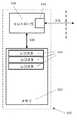
本発明の一実施形態によると、図5に示すように、メモリ機器500は、メモリ機器を最適化するために使用される既定のアクセスプロファイルに対応するために、1つ以上のレジスタ504を含む物理メモリを備えてもよい。メモリ機器500は、特定のアクセスプロファイルをアクティブにするために、通信インターフェース512を介して1つ以上のコマンドを受信するように構成される受信手段510をさらに備えてもよい。本実施形態を理解し易くするために、受信手段510は、コントローラ508とは別の区分を備えるように図示される。しかしながら、受信手段510およびコントローラ508が、単一のエンティティとして実装されてもよいことを理解されたい。1つ以上のコマンドを受信すると、コントローラ508は、メモリレジスタ504に存在する1つ以上のアクセスプロファイルに従って、メモリ機器500を構成してもよい。コントローラ508と物理メモリ502との間の通信は、インターフェース506を介して行われ得る。 According to one embodiment of the present invention, as shown in FIG. 5, the
限定ではなく例として挙げると、既定のアクセスプロファイルの1つは、大きなデータの塊の高速転送を行いやすくし、かつこのような転送前または転送後にホストに「ready」を提供するバーストモードのプロファイルであってもよい。転送時間を最小限に抑えるために、必要なフラッシュメモリ管理処理は転送の後の適当な時間に行われてもよい。例えば、他のアクティビティまたはメモリアクセス処理が起きていない間に行われてもよい。アクセスプロファイルの別の例として、機器上の短いランダムなメモリ位置への迅速なアクセスを可能にするランダムモードプロファイルが挙げられる。
本発明の実施形態に従うメモリ機器は、現在アクティブなアクセスプロファイルを格納するための別のレジスタをさらに備えてもよい。対応する既定のプロファイルのうちのいずれかであり得るこのプロファイルは、メモリ機器への現在のアクセス動作を支配する。例えば、このようなレジスタは、ホストシステムの起動中および/またはメモリ機器の電源が入っている間にアクティブになるデフォルトプロファイルを備えてもよい。このアクティブプロファイルは、メモリ機器の電源を切るまで、または本発明の実施形態に従って、別のプロファイルに置換され得るまで有効であってもよい。本発明に従うメモリ機器の実行時構成の設定可能性は、現在アクティブなプロファイルレジスタのコンテンツを、第1の組のレジスタに格納される既定のプロファイルのうちの1つに置換することによってもたらされる。したがって、新しい種類のメモリアクセスの必要性が生じる場合、コマンドは、適切なプロファイルをアクティブにするように発行されてもよい。コマンドは、デフォルトプロファイルを含むがこれに限定されない既定のアクセスプロファイルのうちのいずれかをアクティブにしてもよい。By way of example and not limitation, one of the default access profiles is a burst mode profile that facilitates high speed transfer of large chunks of data and provides “ready” to the host before or after such transfer. It may be. In order to minimize the transfer time, the necessary flash memory management process may be performed at an appropriate time after the transfer. For example, it may be performed while no other activity or memory access processing is occurring. Another example of an access profile is a random mode profile that allows quick access to short random memory locations on the device.
The memory device according to the embodiment of the present invention may further include another register for storing a currently active access profile. This profile, which can be any of the corresponding default profiles, governs current access operations to the memory device. For example, such a register may comprise a default profile that becomes active during startup of the host system and / or while the memory device is powered on. This active profile may remain in effect until the memory device is turned off or can be replaced with another profile in accordance with embodiments of the present invention. The configurability of the runtime configuration of the memory device according to the present invention is provided by replacing the contents of the currently active profile register with one of the predefined profiles stored in the first set of registers. Thus, if a new type of memory access needs arises, commands may be issued to activate the appropriate profile. The command may activate any of the default access profiles, including but not limited to the default profile.
別の実施形態によると、種々のアクセスプロファイルは、更新されてもよいか、またはメモリ機器にアップロードされてもよい。例えば、既存のアクセスプロファイルは、一定の特徴および機能性を追加または削除するように強化されてもよい(または、新しいバージョンに完全に置換されてもよい)。代替的に、または付加的に、完全に新しいアクセスプロファイルが、メモリ機器にアップロードされてもよいため、メモリ機器を構成するように容易に使用可能である利用可能なアクセスプロファイルの数が増加する。限定ではなく例として、アクセスプロファイルは、アクセスプロファイルの実装に必要なロジックをさらに備えるバイナリファイルとして実装されてもよい。アクセスプロファイルは、メモリ機器ファームウェアの一部であると考えられてもよい。このファームウェアは、最適化された方法においてアクセスの具体的な必要性を処理することを担う。 According to another embodiment, the various access profiles may be updated or uploaded to the memory device. For example, an existing access profile may be enhanced to add or remove certain features and functionality (or may be completely replaced with a new version). Alternatively or additionally, a completely new access profile may be uploaded to the memory device, thus increasing the number of available access profiles that can be readily used to configure the memory device. By way of example and not limitation, the access profile may be implemented as a binary file further comprising the logic necessary to implement the access profile. The access profile may be considered part of the memory device firmware. This firmware is responsible for handling the specific needs of access in an optimized manner.
図1および図2は、本発明の実施形態が実装されてもよい1つの代表的な電子機器12を示す。しかしながら、本発明が、1つの特定の型の機器に限定されるように意図されないことを理解されたい。実際は、本発明の種々の実施形態は、メモリ機器を備えるか、またはメモリ機器にアクセスする任意のスタンドアロン型または内蔵型システムにおける使用に容易に適合され得る。図1および図2の電子機器12は、筺体30、液晶ディスプレイ形式のディスプレイ32、キーパッド34、マイクロホン36、イヤホン38、バッテリ40、赤外線ポート42、アンテナ44、一実施形態に従うUICC形式のスマートカード46、カード読み取り器48、無線インターフェース回路52、コーデック回路54、コントローラ56、およびメモリ58を含む。個々の回路および要素は、全て、当技術分野において、例えば、ノキアの種類の携帯電話機において周知の型を有する。 1 and 2 illustrate one exemplary electronic device 12 in which embodiments of the present invention may be implemented. However, it should be understood that the present invention is not intended to be limited to one particular type of device. In fact, the various embodiments of the present invention can be readily adapted for use in any stand-alone or self-contained system that comprises or has access to a memory device. 1 and 2 includes a
図3は、本発明のある実施形態に従うメモリ機器の実行時構成の設定可能性を示す例示的フロー図である。図3に示すように、ステップ100におけるシステムの起動後に、本発明の実施形態に従うメモリ機器は、ステップ102において、デフォルトプロファイルに従ってそれ自身を構成する。図3において使用する例示的デフォルトプロファイルは、メモリ機器からの大量のシーケンシャルデータの読み取りに対応するようにメモリ機器を構成する。ステップ104において、例えば、ホスト機器のオペレーティングシステムを備え得るシステムは、大量のシーケンシャルデータを読み取る。大量読み取り動作の完了後、システムは、ステップ106において、アイドル状態に入る。アイドル状態中のメモリアクセス動作の大部分は、短いランダム読み取り/書き込み動作を伴う可能性が高いため、メモリ機器は、ステップ108において、短いランダムデータを読み取り/書き込むためのアクセスプロファイルをアクティブにするためにコマンドを受ける。ステップ110において、システムは、大量のシーケンシャル読み取り/書き込みを必要とする。限定することなく例として、この必要性は、システムが外部大容量ストレージ機器に接続される際に生じ得る。このような大容量ストレージ機器には、例えば、USBメモリ等のメモリ機器、または1つ以上の大容量ストレージ構成要素を備えるPCもしくは他の電子機器が含まれ得る。外部メモリ機器を出入りする大量のデータ転送を予測して、本発明の実施形態に従うメモリ機器は、ステップ112において、大量のシーケンシャルデータを読み取り/書き込みするために最適化されるアクセスプロファイルをアクティブにするために、コマンドを受信する。ステップ114において、システムは、大量のシーケンシャル読み取り/書き込み転送の少なくとも一部分を実行する。大量データアクセス動作は、さらなる割り込みを含まずに完了してもよいが、一例示的実施形態では、本発明のシステムは、ステップ116に図示するように、短いランダムI/Oアクセスサイクルにおいてメモリ機器にアクセスする必要があってもよい。本発明の一実施形態によると、ステップ118において、メモリ機器は、長いシーケンシャルデータの読み取り/書き込みを対象とするその現在のアクセスプロファイルを中断するためにコマンドを受信し、短いランダムデータの読み取り/書き込みに最適化される代替アクセスプロファイルをアクティブにしてもよい。システムが、ステップ120において、短いメモリアクセス動作を完了すると、メモリ機器は、ステップ122において、長いシーケンシャルデータを読み取り/書き込みするためのアクセスプロファイルに戻すために、後続のコマンドを受信してもよい。次いで、システムは、ステップ124において、大量のシーケンシャルデータの読み取り/書き込みを再開してもよい。 FIG. 3 is an exemplary flow diagram illustrating the configurability of a runtime configuration of a memory device according to an embodiment of the present invention. As shown in FIG. 3, after the system is started in step 100, the memory device according to the embodiment of the present invention configures itself according to the default profile in step 102. The example default profile used in FIG. 3 configures the memory device to support reading large amounts of sequential data from the memory device. In step 104, for example, a system that may comprise an operating system of the host device reads a large amount of sequential data. After completing the bulk read operation, the system enters an idle state at step 106. Since the majority of memory access operations during idle state are likely to involve short random read / write operations, the memory device activates an access profile for reading / writing short random data in step 108. To receive a command. In step 110, the system requires a large amount of sequential reads / writes. By way of example and not limitation, this need may arise when the system is connected to an external mass storage device. Such mass storage devices may include, for example, a memory device such as a USB memory, or a PC or other electronic device with one or more mass storage components. In anticipation of a large amount of data transfer to and from an external memory device, a memory device according to an embodiment of the present invention activates an access profile that is optimized to read / write a large amount of sequential data in step 112. In order to receive the command. In step 114, the system performs at least a portion of the bulk sequential read / write transfer. A bulk data access operation may be completed without further interruption, but in one exemplary embodiment, the system of the present invention may perform memory device in short random I / O access cycles as illustrated in step 116. You may need to access According to one embodiment of the present invention, at step 118, the memory device receives a command to interrupt its current access profile for long sequential data read / write, and reads / writes short random data. An alternative access profile that is optimized for may be activated. When the system completes the short memory access operation in step 120, the memory device may receive a subsequent command in step 122 to return to the access profile for reading / writing long sequential data. The system may then resume reading / writing large amounts of sequential data at step 124.
上述のように、図3に示す本発明の例示的実施形態は、短いI/Oアクセス動作の実行中に大量のデータ転送を中断する。しかしながら、アプリケーションによっては、2つ以上のメモリアクセス動作を並行して実行することが有利であってもよい。このために、図4は、2つ以上のメモリアクセス動作(およびその対応するアクセスプロファイル)が並行して実装され得る本発明の代替実施形態を図示する。図4において、ステップ200から216は、図3の対応するものとして、類似の動作を表現する。具体的には、ステップ200におけるシステムの起動後に、本発明の実施形態に従うメモリ機器は、ステップ202において、デフォルトプロファイルに従ってそれ自身を構成する。図4において使用する例示的デフォルトプロファイルは、メモリ機器からの大量のシーケンシャルデータの読み取りに対応するようにメモリ機器を構成する。ステップ204において、例えば、ホスト機器のオペレーティングシステムを備えてもよいシステムは、大量のシーケンシャルデータを読み取る。大量読み取り動作の完了後、システムは、ステップ206において、アイドル状態に入る。アイドル状態中のメモリアクセス動作の大部分は、短いランダム読み取り/書き込み動作を伴う可能性が高いため、メモリ機器は、ステップ208において、短いランダムデータを読み取り/書き込むためのアクセスプロファイルをアクティブにするためにコマンドを受ける。次いで、システムは、ステップ210において、大量シーケンシャル読み取り/書き込み機能にアクセスを必要としてもよい。この必要性は、例えば、外部メモリ機器を出入りする大量のデータ転送に備えて生じ得る。本発明の実施形態に従うメモリ機器は、ステップ212において、大量のシーケンシャルデータの読み取り/書き込みのために最適化されるアクセスプロファイルをアクティブにするために、コマンドを受信する。ステップ214において、システムは、大量シーケンシャル読み取り/書き込み転送の少なくとも一部分を行い、その後、ステップ216において、メモリ機器への短い読み取り/書き込みアクセスサイクルのためのシステムの必要性が生じる。図3に従う本発明の例示的実施形態とは対照的に、図4に従う本実施形態は、ステップ220において、短いランダムデータを読み取り/書き込みするために並行アクセスプロファイルをアクティブにするために、本発明の実施形態に従うメモリ機器にコマンドを送ることによって、両方のメモリアクセスモードに対応する。したがって、システムが、ステップ218において、引き続き大量のシーケンシャルデータを読み取り/書き込みする一方で、システムは、同時に(または、インターリーブ様式で)、ステップ222において、短いメモリアクセス動作を実行することができる。 As described above, the exemplary embodiment of the present invention shown in FIG. 3 suspends a large amount of data transfer during the execution of a short I / O access operation. However, depending on the application, it may be advantageous to perform two or more memory access operations in parallel. To this end, FIG. 4 illustrates an alternative embodiment of the invention in which two or more memory access operations (and their corresponding access profiles) can be implemented in parallel. In FIG. 4, steps 200 to 216 represent similar operations as corresponding to FIG. Specifically, after activation of the system in step 200, the memory device according to an embodiment of the present invention configures itself in step 202 according to the default profile. The example default profile used in FIG. 4 configures the memory device to support reading large amounts of sequential data from the memory device. In step 204, for example, a system that may comprise an operating system of the host device reads a large amount of sequential data. After completing the bulk read operation, the system enters an idle state at step 206. Because most of the memory access operations during idle state are likely to involve short random read / write operations, the memory device activates an access profile for reading / writing short random data in step 208. To receive a command. The system may then require access to a bulk sequential read / write function at step 210. This need may arise, for example, in preparation for large amounts of data transfer in and out of external memory devices. A memory device according to an embodiment of the present invention receives a command at step 212 to activate an access profile that is optimized for reading / writing large amounts of sequential data. In step 214, the system performs at least a portion of the bulk sequential read / write transfer, and then in step 216, the need for the system for a short read / write access cycle to the memory device arises. In contrast to the exemplary embodiment of the present invention according to FIG. 3, the present embodiment according to FIG. 4 uses the present invention to activate a concurrent access profile at step 220 to read / write short random data. Both memory access modes are supported by sending commands to the memory device according to the embodiment. Thus, while the system continues to read / write large amounts of sequential data at step 218, the system can perform short memory access operations at step 222 simultaneously (or in an interleaved manner).
図4に従う本発明の実施形態について、2つのみの同時アクセスプロファイルの観点から説明したが、2つ以上のアクセスプロファイルを並行して実装することを可能にするように類似の動作を実行してもよいことも理解できる。この並行的な実装のメモリアクセスプロファイルの1つの具体的な例は、現在のJEDEC JC64 eMMCバージョン4.3(JESD84)と適合するフォーマットにおいて実現されてもよい。EDEC eMMCは、メモリおよびコントローラを備える標準大容量ストレージ機器である。コントローラは、論理ブロック割り当ておよびウェアレベリング等のメモリに関連するブロック管理機能を処理する。また、メモリとホスト機器との間の通信も、標準プロトコルに従って、コントローラによって処理される。このプロトコルは、信号の中でもとりわけ、双方向コマンド信号、機器の初期化に使用されるCMD、およびホストとメモリ機器との間のコマンドの転送を規定する。より具体的には、CMD23(SET_BLOCK_COUNT)は、ブロック(読み取り/書き込み)の数およびブロック読み取り/書き込みコマンドのための確実な書き込みパラメータ(書き込み)を規定する。CMD23は、32ビットの引数フィールドを含み、そのビット15から0は、対応する読み取り/書き込みコマンドのブロックの数を設定するために割り当てられ、ビット30から16は、スタッフビットとして指定される。本発明の一実施形態によると、これらのスタッフビットを利用して、メモリ機器のための異なるアクセスプロファイルを指定してもよい。限定することなく例として、1つのプロファイルは、高速隣接データアクセスモードに対応するバーストプロファイルモードとして規定されてもよい。バーストプロファイルモードの場合、メモリ機器は、全データの受信直後に「exit busy」を標示し、転送モードを「転送状態」に設定してもよいため、ホストによる後続アクセスのより高速な実行が促進される。加えて、第1のアクセスプロファイルに対応するコマンドが依然として実行中である間、メモリ機器は、異なるアクセスプロファイルに対応する追加のコマンドをホストが送信できるようにしてもよい。このように、I/O動作における並列処理の度合いが確立される。さらに、アクセス優先レベルは、アクセス衝突を解決するように規定され、この場合、2つ以上のプロファイルは、並行して実行し、同時に同一のメモリソースへのアクセスを必要とする。このようなメモリリソースの例として、RAMバッファ、フラッシュバス、および他のメモリリソースが挙げられる。 Although the embodiment of the present invention according to FIG. 4 has been described in terms of only two concurrent access profiles, similar operations are performed to allow two or more access profiles to be implemented in parallel. I can understand that. One specific example of this concurrent implementation of the memory access profile may be implemented in a format compatible with the current JEDEC JC64 eMMC version 4.3 (JESD84). EDEC eMMC is a standard mass storage device with memory and controller. The controller handles block management functions related to memory such as logical block allocation and wear leveling. Communication between the memory and the host device is also processed by the controller according to a standard protocol. This protocol defines, among other signals, bidirectional command signals, CMDs used for device initialization, and command transfer between the host and the memory device. More specifically, CMD23 (SET_BLOCK_COUNT) defines the number of blocks (read / write) and certain write parameters (write) for block read / write commands. The CMD 23 includes a 32-bit argument field, bits 15 to 0 of which are assigned to set the number of blocks of the corresponding read / write command, and
本発明の別の実施形態によると、メディア機器に関連するアクセスプロファイルは、メモリ機器の異なるパーティションに関連する異なる制御および/または設定プロファイルを備えるように構成されてもよい。このようなパーティションは、メモリ機器の論理や物理パーティションであってもよい。例えば、一方のパーティションは、ランダム読み取り/書き込み動作のために構成されてもよく、別のパーティションは、シーケンシャルアクセスを提供するように構成されてもよい。 According to another embodiment of the invention, the access profile associated with the media device may be configured with different control and / or configuration profiles associated with different partitions of the memory device. Such a partition may be a logical or physical partition of a memory device. For example, one partition may be configured for random read / write operations and another partition may be configured to provide sequential access.
本発明の別の実施形態によると、メモリアクセス(例えば、I/O読み取り/書き込み)コマンドは、そのアクセスコマンドに対応する好適なアクセスプロファイルを指定するためのメタデータ部分を備えるように構成されてもよい。例えば、本発明に従うシステムは、1つのアドレスが継続的かつ頻繁に更新中であることを認識し、それによってシステムは、そのメモリコマンドに適切なアクセスプロファイルを設定してもよい。メモリ機器(その内部実装および能力に依存する)は、このような持続的かつ具体的なアクセス動作を、特別な特徴を含む物理メモリの一定の区分にマッピングしてもよい。例えば、マッピングは、物理メモリのより耐久性のある性能効率の良い部分、具体的なメモリ技術を利用するメモリの一部分、またはこのような繰り返しアクセス動作により適切に設計される別々の物理チップを対象としてもよい。したがって、メモリ機器のファームウェアは、本発明のある実施形態のアクセスプロファイル要求に従って操作を行い、様々な方式でI/O動作を処理してもよい。 According to another embodiment of the invention, a memory access (eg, I / O read / write) command is configured to include a metadata portion for specifying a preferred access profile corresponding to the access command. Also good. For example, a system according to the present invention may recognize that one address is being updated continuously and frequently, so that the system may set an appropriate access profile for that memory command. A memory device (depending on its internal implementation and capabilities) may map such persistent and specific access operations to certain sections of physical memory that include special features. For example, the mapping may target a more durable, performance-efficient portion of physical memory, a portion of memory that utilizes a specific memory technology, or a separate physical chip that is appropriately designed with such repeated access operations. It is good. Accordingly, the firmware of the memory device may operate according to an access profile request of an embodiment of the present invention and process I / O operations in various ways.
本発明の種々の実施形態は、NAND、大容量メモリ、XiP、および類似の機器等の内蔵メモリ機器、ならびに着脱式メモリカードの両方に同等に適用可能である。 Various embodiments of the present invention are equally applicable to both internal memory devices such as NAND, mass memory, XiP, and similar devices, and removable memory cards.
本明細書において説明する種々の実施形態は、方法ステップまたはプロセスの一般的な内容において説明され、これは、ネットワーク環境におけるコンピュータにより実行されるプログラムコード等の、コンピュータにより実行可能な命令を含むコンピュータ可読媒体において具現化されるコンピュータ製品によって、一実施形態において実装されてもよい。コンピュータ可読媒体は、読み取り専用メモリ(Read Only Memory; ROM)、ランダムアクセスメモリ(Random Access Memory; RAM)、コンパクトディスク(compact disc; CD)、デジタル多用途ディスク(digital versatile disc; DVD)等を含むがこれらに限定されない着脱式および非着脱式ストレージ機器を含んでもよい。概して、プログラムモジュールは、特定のタスクを実行するか、または特定の抽象データ型を実装するルーチン、プログラム、オブジェクト、構成要素、データ構造等を含んでもよい。コンピュータにより実行可能な命令、関連のデータ構造、およびプログラムモジュールは、本明細書に開示する方法のステップを実行するためのプログラムコードの例を表す。特定の一連のこのような実行可能な命令または関連のデータ構造は、このようなステップまたはプロセスにおいて説明する機能を実装するための対応する動作の例を表す。 Various embodiments described herein are described in the general context of method steps or processes, which include computer-executable instructions, such as program code, executed by a computer in a network environment. It may be implemented in one embodiment by a computer product embodied in a readable medium. Computer readable media include read only memory (ROM), random access memory (RAM), compact disc (CD), digital versatile disc (DVD), etc. May include removable and non-removable storage devices that are not limited to these. Generally, program modules may include routines, programs, objects, components, data structures, etc. that perform particular tasks or implement particular abstract data types. Computer-executable instructions, associated data structures, and program modules represent examples of program code for executing steps of the methods disclosed herein. A particular series of such executable instructions or associated data structures represents examples of corresponding operations for implementing the functionality described in such steps or processes.
実施形態に関する前述の説明は、例証目的および説明目的のために提示されている。前述の説明は、包括的であるように、または開示される厳密な形式に本発明の実施形態を限定するように意図されず、上記教示を考慮した変更および変形が可能である。また、これらの変更および変形は、本発明の実施により得られてもよい。本明細書において論じられる実施形態は、種々の実施形態およびその実用的な用途に関する原理および性質を説明し、種々の実施形態における本発明を利用できるように、また想定される特定の使用に適合する種々の変更を有する本発明を当業者が利用できるように、選択および説明されている。本明細書に説明する実施形態の特徴は、方法、装置、モジュール、システム、およびコンピュータプログラム製品の全ての可能な組み合わせで組み合わせられてもよい。 The foregoing description of the embodiments has been presented for purposes of illustration and description. The foregoing description is not intended to be exhaustive or to limit the embodiments of the invention to the precise form disclosed, and modifications and variations are possible in light of the above teachings. Moreover, these changes and modifications may be obtained by implementing the present invention. The embodiments discussed herein explain the principles and properties of various embodiments and their practical applications, and are adapted to the particular use envisaged so that the invention can be utilized in various embodiments. The present invention with various modifications has been selected and described so that those skilled in the art can utilize it. The features of the embodiments described herein may be combined in all possible combinations of methods, apparatus, modules, systems, and computer program products.
本願の親出願(特願2010−548134)の出願当初の特許請求の範囲に記載の実施形態は次の通りである。
(1)メモリ機器へのアクセスを構成するための方法であって、
前記メモリ機器に関連する1つ以上のアクセスプロファイルをアクティブにするための1つ以上のコマンドを受信することと、
前記アクセスプロファイルのうちの少なくとも1つに従って前記メモリ機器へのアクセスを構成することと、
を含む、方法。
(2)前記1つ以上のアクセスプロファイルは、ランダムモードおよびシーケンシャルモードのアクセスのうちの少なくとも1つに対応する、(1)に記載の方法。
(3)前記アクセスプロファイルは、読み取り、書き込み、消去、および変更のうちの少なくとも1つの属性操作に対応する、(2)に記載の方法。
(4)前記1つ以上のアクセスプロファイルは、前記メモリ機器の同一アドレスへの繰り返しのアクセス要求に対応するように適合される、(1)に記載の方法。
(5)前記1つ以上のアクセスプロファイルは、前記メモリ機器に関連する最適化性能を生成するように適合される、(1)に記載の方法。
(6)前記性能は、前記メモリ機器に関連するデータスループット、寿命、および電力消費のうちの少なくとも1つに従って最適化される、(5)に記載の方法。
(7)前記1つ以上のコマンドは、前記コマンドに対応する好適なアクセスプロファイルを指定するためのメタデータ部分を備える、(1)に記載の方法。
(8)特定のメモリ位置は、前記アクセスプロファイルに従って利用される、(7)に記載の方法。
(9)前記特定のメモリ位置は、特別な特徴を含む前記メモリ機器の区分を備える、(8)に記載の方法。
(10)前記特定のメモリ位置は、別々の物理メモリチップを備える、(8)に記載の方法。
(11)前記1つ以上のアクセスプロファイルは、前記メモリ機器の1つ以上のパーティションに関連する、(1)に記載の方法。
(12)前記構成することは、2つ以上のアクセスプロファイルについて並行して適合される、(1)に記載の方法。
(13)前記構成することは、eMMCのJESD84規格に従って実行される、(12)に記載の方法。
(14)メモリリソースへの同時のアクセス衝突を解決するために、アクセス優先レベルを指定することをさらに含む、(12)に記載の方法。
(15)前記メモリ機器は、大容量メモリおよびシステムメモリの両方の実装をもたらすために使用される、(1)に記載の方法。
(16)電源を入れた後に前記メモリ機器を構成するように使用されるデフォルトアクセスプロファイルをさらに備える、(1)に記載の方法。
(17)メモリ機器であって、
前記メモリ機器に関連する1つ以上の既定のアクセスプロファイルを格納するための1つ以上のレジスタと、
前記メモリ機器に関連する1つ以上のアクセスプロファイルをアクティブにするための1つ以上のコマンドを受信するための受信手段と、
前記既定のアクセスプロファイルのうちの少なくとも1つに従って、前記メモリ機器へのアクセスを構成するための構成手段と、
を備える、メモリ機器。
(18)前記1つ以上のアクセスプロファイルは、ランダムおよびシーケンシャルモードのアクセスのうちの少なくとも1つに対応する、(17)に記載のメモリ機器。
(19)前記アクセスプロファイルは、読み取り、書き込み、消去、および変更のうちの少なくとも1つの属性操作に対応する、(18)に記載のメモリ機器。
(20)前記1つ以上のアクセスプロファイルは、前記メモリ機器の同一アドレスへの繰り返しのアクセス要求に対応するように適合される、(17)に記載のメモリ機器。
(21)前記1つ以上のアクセスプロファイルは、前記メモリ機器に関連する最適化性能を生成するように適合される、(17)に記載のメモリ機器。
(22)前記性能は、前記メモリ機器に関連するデータスループット、寿命、および電力消費のうちの少なくとも1つに従って最適化される、(21)に記載のメモリ機器。
(23)前記1つ以上のコマンドは、前記コマンドに対応する好適なアクセスプロファイルを指定するためのメタデータ部分を備える、(17)に記載のメモリ機器。
(24)特定のメモリ位置は、前記アクセスプロファイルに従って利用される、(23)に記載のメモリ機器。
(25)前記特定のメモリ位置は、特別な特徴を含む前記メモリ機器の区分を備える、(24)に記載のメモリ機器。
(26)前記特定のメモリ位置は、別々の物理メモリチップを備える、(24)に記載のメモリ機器。
(27)前記1つ以上のアクセスプロファイルは、前記メモリ機器の1つ以上のパーティションに関連する、(17)に記載のメモリ機器。
(28)前記構成することは、2つ以上のアクセスプロファイルについて並行して適合される、(17)に記載のメモリ機器。
(29)前記構成することは、eMMCのJESD84規格に従って実行される、(28)に記載のメモリ機器。
(30)メモリリソースへの同時のアクセス衝突を解決するために、アクセス優先レベルを指定するための手段をさらに備える、(28)に記載のメモリ機器。
(31)前記メモリ機器は、大容量メモリおよびシステムメモリの両方の実装をもたらすために使用される、(17)に記載のメモリ機器。
(32)電源を入れた後に前記メモリ機器を構成するように使用されるデフォルトアクセスプロファイルをさらに備える、(17)に記載のメモリ機器。
(33)前記既定のアクセスプロファイルのうちの1つ以上は、前記アクセスプロファイルの新しいバージョンで更新される、(17)に記載のメモリ機器。
(34)現在アクティブなアクセスプロファイルは、指定のメモリレジスタに存在する、(17)に記載のメモリ機器。
(35)コンピュータ可読媒体上に具現化されるコンピュータプログラム製品であって、
前記メモリ機器に関連する1つ以上のアクセスプロファイルをアクティブにするための1つ以上のコマンドを受信するためのコンピュータコードと、
前記アクセスプロファイルのうちの少なくとも1つに従って前記メモリ機器へのアクセスを構成するためのコンピュータコードと、
を備える、コンピュータプログラム製品。
(36)メモリ機器にアクセスするためのシステムであって、
前記メモリ機器に関連する1つ以上のアクセスプロファイルをアクティブにするための1つ以上のコマンドを受信するためのエンティティと、
前記アクセスプロファイルのうちの少なくとも1つに従って前記メモリ機器へのアクセスを構成するためのエンティティと、
を備える、システム。
(37)メモリ機器にアクセスするためのシステムであって、
前記メモリ機器のアクセスの必要性に従って、1つ以上のコマンドを発行するためのホストと、
前記コマンドを受信し、少なくとも1つ以上のアクセスプロファイルに従って、前記メモリ機器へのアクセスを構成するためのエンティティと、
を備える、システム。The embodiment described in the scope of claims of the present application of the parent application (Japanese Patent Application No. 2010-548134) of the present application is as follows.
(1) A method for configuring access to a memory device, comprising:
Receiving one or more commands to activate one or more access profiles associated with the memory device;
Configuring access to the memory device according to at least one of the access profiles;
Including a method.
(2) The method according to (1), wherein the one or more access profiles correspond to at least one of a random mode access and a sequential mode access.
(3) The method according to (2), wherein the access profile corresponds to at least one attribute operation of read, write, erase, and change.
(4) The method of (1), wherein the one or more access profiles are adapted to accommodate repeated access requests to the same address of the memory device.
(5) The method of (1), wherein the one or more access profiles are adapted to generate optimized performance associated with the memory device.
(6) The method of (5), wherein the performance is optimized according to at least one of data throughput, lifetime, and power consumption associated with the memory device.
(7) The method of (1), wherein the one or more commands comprise a metadata portion for specifying a suitable access profile corresponding to the command.
(8) The method of (7), wherein a specific memory location is utilized according to the access profile.
(9) The method of (8), wherein the particular memory location comprises a section of the memory device that includes special features.
(10) The method of (8), wherein the specific memory location comprises a separate physical memory chip.
(11) The method of (1), wherein the one or more access profiles are associated with one or more partitions of the memory device.
(12) The method of (1), wherein the configuring is adapted in parallel for two or more access profiles.
(13) The method according to (12), wherein the configuring is performed in accordance with eMMC's JESD84 standard.
(14) The method according to (12), further comprising specifying an access priority level in order to resolve simultaneous access conflicts to memory resources.
(15) The method of (1), wherein the memory device is used to provide an implementation of both mass memory and system memory.
(16) The method according to (1), further comprising a default access profile used to configure the memory device after being turned on.
(17) A memory device,
One or more registers for storing one or more predefined access profiles associated with the memory device;
Receiving means for receiving one or more commands for activating one or more access profiles associated with the memory device;
Configuring means for configuring access to the memory device according to at least one of the predetermined access profiles;
A memory device.
(18) The memory device according to (17), wherein the one or more access profiles correspond to at least one of random and sequential mode accesses.
(19) The memory device according to (18), wherein the access profile corresponds to at least one attribute operation of read, write, erase, and change.
(20) The memory device of (17), wherein the one or more access profiles are adapted to accommodate repeated access requests to the same address of the memory device.
(21) The memory device of (17), wherein the one or more access profiles are adapted to generate optimized performance associated with the memory device.
(22) The memory device of (21), wherein the performance is optimized according to at least one of data throughput, lifetime, and power consumption associated with the memory device.
(23) The memory device according to (17), wherein the one or more commands include a metadata portion for designating a suitable access profile corresponding to the command.
(24) The memory device according to (23), wherein the specific memory location is used according to the access profile.
(25) The memory device of (24), wherein the particular memory location comprises a section of the memory device that includes special features.
(26) The memory device of (24), wherein the specific memory location comprises a separate physical memory chip.
(27) The memory device according to (17), wherein the one or more access profiles are related to one or more partitions of the memory device.
(28) The memory device according to (17), wherein the configuring is adapted in parallel for two or more access profiles.
(29) The memory device according to (28), wherein the configuring is executed in accordance with eMMC's JESD84 standard.
(30) The memory device according to (28), further comprising means for designating an access priority level in order to resolve a simultaneous access collision to a memory resource.
(31) The memory device according to (17), wherein the memory device is used to provide an implementation of both a mass memory and a system memory.
(32) The memory device according to (17), further comprising a default access profile used to configure the memory device after power is turned on.
(33) The memory device according to (17), wherein one or more of the predetermined access profiles are updated with a new version of the access profile.
(34) The memory device according to (17), wherein the currently active access profile exists in a specified memory register.
(35) A computer program product embodied on a computer-readable medium,
Computer code for receiving one or more commands for activating one or more access profiles associated with the memory device;
Computer code for configuring access to the memory device according to at least one of the access profiles;
A computer program product comprising:
(36) A system for accessing a memory device,
An entity for receiving one or more commands to activate one or more access profiles associated with the memory device;
An entity for configuring access to the memory device according to at least one of the access profiles;
A system comprising:
(37) A system for accessing a memory device,
A host for issuing one or more commands according to the memory device access needs;
An entity for receiving the command and configuring access to the memory device according to at least one or more access profiles;
A system comprising:
Claims (34)
Translated fromJapanese前記メモリ機器の少なくとも一つの使われ方のために該メモリ機器へのアクセスがどのように設定されるかを定める、一つ又は複数の設定情報と、コントローラとを備え、前記コントローラは、
前記メモリ機器に関連する一つ又は複数の設定情報の少なくとも一つをアクティブ化する一つ又は複数の命令を受信するように構成されると共に、
前記少なくとも一つの使われ方のための前記一つ又は複数の設定情報に従って、前記メモリ機器の少なくとも一部が設定されるように、前記一つ又は複数の命令の少なくとも一部に基づいて、前記一つ又は複数の設定情報に従って、前記メモリ機器へのアクセスを設定するように構成される、
メモリ機器。A memory device,
One or more setting information that defines how access to the memory device is set for at least one usage of the memory device, and a controller, the controller comprising:
Configured to receive one or more instructions to activate at least one of the one or more configuration information associated with the memory device;
Based on at least a portion of the one or more instructions, such that at least a portion of the memory device is configured according to the one or more configuration information for the at least one usage. Configured to configure access to the memory device according to one or more configuration information;
Memory equipment.
前記少なくとも一つの使われ方のための前記一つ又は複数の設定情報に従って、前記メモリ機器の少なくとも一部が設定されるように、前記一つ又は複数の命令の少なくとも一部に基づいて、前記一つ又は複数の設定情報に従って、前記メモリ機器へのアクセスを設定することと;
を含む、方法。Receiving one or more instructions for activating at least one of the one or more configuration information associated with the memory device, wherein the one or more configuration information is used by at least one usage of the memory device; Said receiving, which defines how access to the memory device is set for us;
Based on at least a portion of the one or more instructions, such that at least a portion of the memory device is configured according to the one or more configuration information for the at least one usage. Setting access to the memory device according to one or more setting information;
Including a method.
前記ホスト装置をメモリ機器に接続するインタフェースと、処理を実行するためのロジック命令により設定されたコントローラとを備え、前記処理は、前記ホスト装置から、該ホスト装置に接続された前記メモリデバイスに、一つ又は複数の命令を送信することを含み、ここで前記一つ又は複数の命令は、
メモリ機器に関連する一つ又は複数の設定情報の少なくとも一つをアクティブ化すること 、ただし前記一つ又は複数の設定情報は、前記メモリ機器の少なくとも一つの使われ方のために該メモリ機器へのアクセスがどのように設定されるかを定める、前記アクティブ化することと;
前記少なくとも一つの使われ方のための前記一つ又は複数の設定情報に従って、前記メモリ機器の少なくとも一部が設定されるように、前記一つ又は複数の設定情報に従って、前記メモリ機器へのアクセスを設定することと;
のための命令である、ホスト装置。A host device,
An interface for connecting the host device to a memory device and a controller set by a logic instruction for executing processing, the processing from the host device to the memory device connected to the host device, Sending one or more instructions, wherein the one or more instructions are:
Activating at least one of the one or more configuration information associated with the memory device, wherein the one or more configuration information is sent to the memory device for at least one usage of the memory device. Activating to define how access is set up;
Access to the memory device according to the one or more setting information, such that at least a part of the memory device is set according to the one or more setting information for the at least one usage. And setting;
A host device that is a command for.
前記メモリ機器の少なくとも一つの使われ方のために該メモリ機器へのアクセスがどのように設定されるかを定める、一つ又は複数の設定情報と;
コントローラと、
を備え、前記コントローラは、
前記メモリ機器に関連する一つ又は複数の設定情報の少なくとも一つをアクティブ化する一つ又は複数の命令を受信すること 、ただし前記一つ又は複数の命令は、該一つ又は複数の命令に対応する前記一つ又は複数の設定情報の少なくとも一つを指定するメタデータ部分を有する、前記受信することと;
前記少なくとも一つの使われ方のための前記一つ又は複数の設定情報に従って、前記メモリ機器の少なくとも一部が設定されるように、前記一つ又は複数の命令の少なくとも一部に基づいて、前記一つ又は複数の設定情報に従って、前記メモリ機器へのアクセスを設定することと;
を行うように構成される、メモリ機器。A memory device,
One or more configuration information defining how access to the memory device is configured for at least one usage of the memory device;
A controller,
The controller comprises:
Receiving one or more commands for activating at least one of the one or more configuration information associated with the memory device, wherein the one or more commands are included in the one or more commands. Receiving the metadata portion specifying at least one of the corresponding one or more setting information;
Based on at least a portion of the one or more instructions, such that at least a portion of the memory device is configured according to the one or more configuration information for the at least one usage. Setting access to the memory device according to one or more setting information;
A memory device configured to do.
Applications Claiming Priority (2)
| Application Number | Priority Date | Filing Date | Title |
|---|---|---|---|
| US12/039,672 | 2008-02-28 | ||
| US12/039,672US8307180B2 (en) | 2008-02-28 | 2008-02-28 | Extended utilization area for a memory device |
Related Parent Applications (1)
| Application Number | Title | Priority Date | Filing Date |
|---|---|---|---|
| JP2013103695ADivisionJP2013211033A (en) | 2008-02-28 | 2013-05-16 | Expanded utilization range for memory device |
Related Child Applications (1)
| Application Number | Title | Priority Date | Filing Date |
|---|---|---|---|
| JP2017156699ADivisionJP6602823B2 (en) | 2008-02-28 | 2017-08-15 | Extended usage range for memory devices |
Publications (1)
| Publication Number | Publication Date |
|---|---|
| JP2015164074Atrue JP2015164074A (en) | 2015-09-10 |
Family
ID=41014077
Family Applications (7)
| Application Number | Title | Priority Date | Filing Date |
|---|---|---|---|
| JP2010548134AActiveJP5663720B2 (en) | 2008-02-28 | 2009-01-30 | Extended usage range for memory devices |
| JP2013103695APendingJP2013211033A (en) | 2008-02-28 | 2013-05-16 | Expanded utilization range for memory device |
| JP2015099731APendingJP2015164074A (en) | 2008-02-28 | 2015-05-15 | Extended usage range for memory devices |
| JP2017156699AActiveJP6602823B2 (en) | 2008-02-28 | 2017-08-15 | Extended usage range for memory devices |
| JP2019185570APendingJP2020074079A (en) | 2008-02-28 | 2019-10-09 | Extended usage range for memory devices |
| JP2021069406APendingJP2021108199A (en) | 2008-02-28 | 2021-04-16 | Range of expansion usage for memory apparatus |
| JP2023021268APendingJP2023055992A (en) | 2008-02-28 | 2023-02-15 | Extended utilization range for memory device |
Family Applications Before (2)
| Application Number | Title | Priority Date | Filing Date |
|---|---|---|---|
| JP2010548134AActiveJP5663720B2 (en) | 2008-02-28 | 2009-01-30 | Extended usage range for memory devices |
| JP2013103695APendingJP2013211033A (en) | 2008-02-28 | 2013-05-16 | Expanded utilization range for memory device |
Family Applications After (4)
| Application Number | Title | Priority Date | Filing Date |
|---|---|---|---|
| JP2017156699AActiveJP6602823B2 (en) | 2008-02-28 | 2017-08-15 | Extended usage range for memory devices |
| JP2019185570APendingJP2020074079A (en) | 2008-02-28 | 2019-10-09 | Extended usage range for memory devices |
| JP2021069406APendingJP2021108199A (en) | 2008-02-28 | 2021-04-16 | Range of expansion usage for memory apparatus |
| JP2023021268APendingJP2023055992A (en) | 2008-02-28 | 2023-02-15 | Extended utilization range for memory device |
Country Status (6)
| Country | Link |
|---|---|
| US (11) | US8307180B2 (en) |
| EP (2) | EP2248023B1 (en) |
| JP (7) | JP5663720B2 (en) |
| KR (2) | KR101468824B1 (en) |
| CN (2) | CN101952808B (en) |
| WO (1) | WO2009106680A1 (en) |
Families Citing this family (28)
| Publication number | Priority date | Publication date | Assignee | Title |
|---|---|---|---|---|
| US8307180B2 (en) | 2008-02-28 | 2012-11-06 | Nokia Corporation | Extended utilization area for a memory device |
| US8874824B2 (en) | 2009-06-04 | 2014-10-28 | Memory Technologies, LLC | Apparatus and method to share host system RAM with mass storage memory RAM |
| US8307151B1 (en)* | 2009-11-30 | 2012-11-06 | Micron Technology, Inc. | Multi-partitioning feature on e-MMC |
| WO2012065112A2 (en) | 2010-11-12 | 2012-05-18 | Apple Inc. | Apparatus and methods for recordation of device history across multiple software emulations |
| CN102170548A (en)* | 2011-01-28 | 2011-08-31 | 杭州海康威视数字技术股份有限公司 | Mutually exclusive resource remote-access method and digital video recorder |
| US8751728B1 (en) | 2011-04-29 | 2014-06-10 | Western Digital Technologies, Inc. | Storage system bus transfer optimization |
| EP2798500A1 (en) | 2011-12-29 | 2014-11-05 | Memory Technologies LLC | Method for erasing data entity in memory module |
| US9417998B2 (en) | 2012-01-26 | 2016-08-16 | Memory Technologies Llc | Apparatus and method to provide cache move with non-volatile mass memory system |
| US9311226B2 (en) | 2012-04-20 | 2016-04-12 | Memory Technologies Llc | Managing operational state data of a memory module using host memory in association with state change |
| US9009570B2 (en)* | 2012-06-07 | 2015-04-14 | Micron Technology, Inc. | Integrity of an address bus |
| US8910017B2 (en) | 2012-07-02 | 2014-12-09 | Sandisk Technologies Inc. | Flash memory with random partition |
| US9519428B2 (en)* | 2012-09-26 | 2016-12-13 | Qualcomm Incorporated | Dynamically improving performance of a host memory controller and a memory device |
| US9569352B2 (en) | 2013-03-14 | 2017-02-14 | Sandisk Technologies Llc | Storage module and method for regulating garbage collection operations based on write activity of a host |
| US9766823B2 (en) | 2013-12-12 | 2017-09-19 | Memory Technologies Llc | Channel optimized storage modules |
| US9471254B2 (en)* | 2014-04-16 | 2016-10-18 | Sandisk Technologies Llc | Storage module and method for adaptive burst mode |
| US9928169B2 (en) | 2014-05-07 | 2018-03-27 | Sandisk Technologies Llc | Method and system for improving swap performance |
| US9710198B2 (en) | 2014-05-07 | 2017-07-18 | Sandisk Technologies Llc | Method and computing device for controlling bandwidth of swap operations |
| US9665296B2 (en) | 2014-05-07 | 2017-05-30 | Sandisk Technologies Llc | Method and computing device for using both volatile memory and non-volatile swap memory to pre-load a plurality of applications |
| US9633233B2 (en) | 2014-05-07 | 2017-04-25 | Sandisk Technologies Llc | Method and computing device for encrypting data stored in swap memory |
| CN105337944B (en)* | 2014-08-12 | 2020-02-21 | 格马尔托股份有限公司 | Method for managing several profiles in a secure element |
| US10101763B2 (en)* | 2015-07-29 | 2018-10-16 | Sandisk Technologies Inc. | Interface adjustment processes for a data storage device |
| CN110727399B (en)* | 2015-09-18 | 2021-09-03 | 华为技术有限公司 | Storage array management method and device |
| US9977603B2 (en)* | 2016-05-02 | 2018-05-22 | Micron Technology, Inc. | Memory devices for detecting known initial states and related methods and electronic systems |
| US9990158B2 (en) | 2016-06-22 | 2018-06-05 | Sandisk Technologies Llc | Storage system and method for burst mode management using transfer RAM |
| KR102430983B1 (en) | 2017-09-22 | 2022-08-09 | 삼성전자주식회사 | Storage device and method of operating the same |
| FR3099258B1 (en)* | 2019-07-26 | 2022-06-24 | Idemia Identity & Security France | Dynamic adaptation of a secure element execution environment to profiles |
| US11516431B2 (en) | 2020-07-30 | 2022-11-29 | Microsoft Technology Licensing, Llc | Meeting privacy protection system |
| US11600312B1 (en) | 2021-08-16 | 2023-03-07 | Micron Technology, Inc. | Activate commands for memory preparation |
Citations (8)
| Publication number | Priority date | Publication date | Assignee | Title |
|---|---|---|---|---|
| JPH0268671A (en)* | 1988-09-02 | 1990-03-08 | Matsushita Electric Ind Co Ltd | image memory |
| JPH06236681A (en)* | 1993-02-12 | 1994-08-23 | Toshiba Corp | Semiconductor memory |
| JP2000067584A (en)* | 1998-07-31 | 2000-03-03 | Samsung Electronics Co Ltd | Mode register and nonvolatile semiconductor memory device |
| US20020040437A1 (en)* | 2000-09-29 | 2002-04-04 | Mitsubishi Denki Kabushiki Kaisha | Semiconductor memory device internally provided with logic circuit which can be readily controlled and controlling method thereof |
| US20020118593A1 (en)* | 2001-02-27 | 2002-08-29 | Fujitsu Limited | Memory system |
| WO2004084231A1 (en)* | 2003-03-19 | 2004-09-30 | Koninklijke Philips Electronics N.V. | Universal memory device having a profil storage unit |
| US20050204113A1 (en)* | 2004-03-09 | 2005-09-15 | International Business Machines Corp. | Method, system and storage medium for dynamically selecting a page management policy for a memory controller |
| US20070192527A1 (en)* | 2006-02-16 | 2007-08-16 | Fujitsu Limited | Memory system |
Family Cites Families (302)
| Publication number | Priority date | Publication date | Assignee | Title |
|---|---|---|---|---|
| US3653001A (en) | 1967-11-13 | 1972-03-28 | Bell Telephone Labor Inc | Time-shared computer graphics system having data processing means at display terminals |
| JPS59135563A (en) | 1983-01-24 | 1984-08-03 | Hitachi Ltd | Computer system with disk/cache device |
| JPS59135563U (en) | 1983-02-28 | 1984-09-10 | ダイセル化学工業株式会社 | optical disc container |
| CA1293819C (en) | 1986-08-29 | 1991-12-31 | Thinking Machines Corporation | Very large scale computer |
| JPS6464073A (en) | 1987-09-03 | 1989-03-09 | Minolta Camera Kk | Image memory |
| JP2804115B2 (en)* | 1988-09-19 | 1998-09-24 | 株式会社日立製作所 | Disk file system |
| JP2661224B2 (en) | 1988-12-23 | 1997-10-08 | 株式会社リコー | Memory expansion method |
| US5781753A (en) | 1989-02-24 | 1998-07-14 | Advanced Micro Devices, Inc. | Semi-autonomous RISC pipelines for overlapped execution of RISC-like instructions within the multiple superscalar execution units of a processor having distributed pipeline control for speculative and out-of-order execution of complex instructions |
| JP3038781B2 (en)* | 1989-04-21 | 2000-05-08 | 日本電気株式会社 | Memory access control circuit |
| JPH0679293B2 (en) | 1990-10-15 | 1994-10-05 | 富士通株式会社 | Computer system |
| US5680570A (en) | 1991-06-12 | 1997-10-21 | Quantum Corporation | Memory system with dynamically allocatable non-volatile storage capability |
| JP3407317B2 (en) | 1991-11-28 | 2003-05-19 | 株式会社日立製作所 | Storage device using flash memory |
| WO1993018461A1 (en) | 1992-03-09 | 1993-09-16 | Auspex Systems, Inc. | High-performance non-volatile ram protected write cache accelerator system |
| US5809340A (en)* | 1993-04-30 | 1998-09-15 | Packard Bell Nec | Adaptively generating timing signals for access to various memory devices based on stored profiles |
| JPH07105095A (en) | 1993-10-04 | 1995-04-21 | Fuji Electric Co Ltd | Cache control method for disk storage device |
| EP0686971B1 (en) | 1994-06-07 | 2002-02-06 | Hitachi, Ltd. | Information storing device and method for controlling same to record/reproduce information by selecting one of working modes |
| US5710931A (en) | 1994-09-07 | 1998-01-20 | Canon Kabushiki Kaisha | Suspension state control for information processing devices such as battery powered computers |
| JP3687115B2 (en) | 1994-10-27 | 2005-08-24 | ソニー株式会社 | Playback device |
| JPH08161216A (en) | 1994-12-09 | 1996-06-21 | Toshiba Corp | Information processing device with high-speed memory clear function |
| US5586291A (en) | 1994-12-23 | 1996-12-17 | Emc Corporation | Disk controller with volatile and non-volatile cache memories |
| EP0749063A3 (en) | 1995-06-07 | 1999-01-13 | International Business Machines Corporation | Method and apparatus for suspend/resume operation in a computer |
| IT235879Y1 (en) | 1995-06-14 | 2000-07-18 | Olivetti & Co Spa | KEYBOARD FOR DATA INTRODUCTION WITH TRACK POSITIONER |
| US5845313A (en) | 1995-07-31 | 1998-12-01 | Lexar | Direct logical block addressing flash memory mass storage architecture |
| US6393492B1 (en) | 1995-11-03 | 2002-05-21 | Texas Instruments Incorporated | Method and arrangement for operating a mass memory storage peripheral computer device connected to a host computer |
| US5802069A (en) | 1995-11-13 | 1998-09-01 | Intel Corporation | Implementing mass storage device functions using host processor memory |
| US5822553A (en) | 1996-03-13 | 1998-10-13 | Diamond Multimedia Systems, Inc. | Multiple parallel digital data stream channel controller architecture |
| US5838873A (en) | 1996-05-31 | 1998-11-17 | Thomson Consumer Electronics, Inc. | Packetized data formats for digital data storage media |
| US5805882A (en) | 1996-07-19 | 1998-09-08 | Compaq Computer Corporation | Computer system and method for replacing obsolete or corrupt boot code contained within reprogrammable memory with new boot code supplied from an external source through a data port |
| JPH10228413A (en) | 1997-02-17 | 1998-08-25 | Ge Yokogawa Medical Syst Ltd | Memory access controlling method device therefor and memory system |
| JPH10240607A (en)* | 1997-02-26 | 1998-09-11 | Toshiba Corp | Memory system |
| US5933626A (en) | 1997-06-12 | 1999-08-03 | Advanced Micro Devices, Inc. | Apparatus and method for tracing microprocessor instructions |
| JPH11143643A (en) | 1997-11-06 | 1999-05-28 | Sony Corp | Reproducing device and cache processing method |
| US6226710B1 (en) | 1997-11-14 | 2001-05-01 | Utmc Microelectronic Systems Inc. | Content addressable memory (CAM) engine |
| US5924097A (en) | 1997-12-23 | 1999-07-13 | Unisys Corporation | Balanced input/output task management for use in multiprocessor transaction processing system |
| JP4310821B2 (en) | 1997-12-24 | 2009-08-12 | ソニー株式会社 | Information recording apparatus and method |
| JP3990485B2 (en) | 1997-12-26 | 2007-10-10 | 株式会社ルネサステクノロジ | Semiconductor nonvolatile memory device |
| JPH11259357A (en) | 1998-03-09 | 1999-09-24 | Seiko Epson Corp | Semiconductor integrated device and nonvolatile memory writing method |
| US5999876A (en) | 1998-04-01 | 1999-12-07 | Cummins Engine Company, Inc. | Method and system for communication with an engine control module in sleep mode |
| US6173425B1 (en) | 1998-04-15 | 2001-01-09 | Integrated Device Technology, Inc. | Methods of testing integrated circuits to include data traversal path identification information and related status information in test data streams |
| US6067300A (en) | 1998-06-11 | 2000-05-23 | Cabletron Systems, Inc. | Method and apparatus for optimizing the transfer of data packets between local area networks |
| JP3585091B2 (en)* | 1998-06-15 | 2004-11-04 | 富士通株式会社 | Storage device |
| US6021076A (en) | 1998-07-16 | 2000-02-01 | Rambus Inc | Apparatus and method for thermal regulation in memory subsystems |
| JP2000057039A (en) | 1998-08-03 | 2000-02-25 | Canon Inc | Access control method and device, file system, and information processing device |
| US6721288B1 (en) | 1998-09-16 | 2004-04-13 | Openwave Systems Inc. | Wireless mobile devices having improved operation during network unavailability |
| CA2345123A1 (en) | 1998-09-28 | 2000-04-06 | T Squared G Incorporated | Multibyte random access mass storage/memory system |
| US6279114B1 (en) | 1998-11-04 | 2001-08-21 | Sandisk Corporation | Voltage negotiation in a single host multiple cards system |
| JP2000181784A (en)* | 1998-12-18 | 2000-06-30 | Hitachi Ltd | Rewritable nonvolatile storage device |
| JP2001006379A (en) | 1999-06-16 | 2001-01-12 | Fujitsu Ltd | Flash memory with copy and move functions |
| US7889544B2 (en) | 2004-04-05 | 2011-02-15 | Super Talent Electronics, Inc. | High-speed controller for phase-change memory peripheral device |
| US7702831B2 (en) | 2000-01-06 | 2010-04-20 | Super Talent Electronics, Inc. | Flash memory controller for electronic data flash card |
| US6513094B1 (en) | 1999-08-23 | 2003-01-28 | Advanced Micro Devices, Inc. | ROM/DRAM data bus sharing with write buffer and read prefetch activity |
| JP2001067786A (en)* | 1999-08-30 | 2001-03-16 | Matsushita Electric Ind Co Ltd | Recording and playback device |
| US6757797B1 (en) | 1999-09-30 | 2004-06-29 | Fujitsu Limited | Copying method between logical disks, disk-storage system and its storage medium |
| US6665747B1 (en) | 1999-10-22 | 2003-12-16 | Sun Microsystems, Inc. | Method and apparatus for interfacing with a secondary storage system |
| KR20020050270A (en) | 1999-11-09 | 2002-06-26 | 토토라노 제이. 빈센트 | Dynamically adjusting a processor's operational parameters according to its environment |
| US20060075395A1 (en) | 2004-10-01 | 2006-04-06 | Lee Charles C | Flash card system |
| US7552251B2 (en)* | 2003-12-02 | 2009-06-23 | Super Talent Electronics, Inc. | Single-chip multi-media card/secure digital (MMC/SD) controller reading power-on boot code from integrated flash memory for user storage |
| US6609182B1 (en) | 2000-01-20 | 2003-08-19 | Microsoft Corporation | Smart hibernation on an operating system with page translation |
| JP3955712B2 (en) | 2000-03-03 | 2007-08-08 | 株式会社ルネサステクノロジ | Semiconductor device |
| JP4524439B2 (en)* | 2000-03-30 | 2010-08-18 | ラウンド ロック リサーチ、エルエルシー | Synchronous flash memory with zero latency and zero bus turnaround functions |
| US6785764B1 (en)* | 2000-05-11 | 2004-08-31 | Micron Technology, Inc. | Synchronous flash memory with non-volatile mode register |
| US20020000931A1 (en) | 2000-04-14 | 2002-01-03 | Mark Petronic | User interface for a two-way satellite communication system |
| US6396744B1 (en) | 2000-04-25 | 2002-05-28 | Multi Level Memory Technology | Flash memory with dynamic refresh |
| US6681304B1 (en) | 2000-06-30 | 2004-01-20 | Intel Corporation | Method and device for providing hidden storage in non-volatile memory |
| US6721843B1 (en) | 2000-07-07 | 2004-04-13 | Lexar Media, Inc. | Flash memory architecture implementing simultaneously programmable multiple flash memory banks that are host compatible |
| JP2002023962A (en) | 2000-07-07 | 2002-01-25 | Fujitsu Ltd | Disk device and its controlling method |
| JP3965874B2 (en) | 2000-07-17 | 2007-08-29 | セイコーエプソン株式会社 | Recording method for printing on recording medium using two liquids, recorded matter printed by this recording method, and recording apparatus comprising means for executing this recording method |
| DE10196440B4 (en)* | 2000-07-18 | 2006-03-23 | Intel Corporation, Santa Clara | Control access to multiple isolated storage in an isolated execution environment |
| WO2002026875A1 (en) | 2000-09-25 | 2002-04-04 | Stepan Company | Alkoxylated phosphate esters useful as secondary adhesion promoters, internal mold release agents and viscosity modifiers |
| US6804763B1 (en) | 2000-10-17 | 2004-10-12 | Igt | High performance battery backed ram interface |
| EP1199723B1 (en)* | 2000-10-18 | 2008-12-31 | STMicroelectronics S.r.l. | Interlaced memory device with random or sequential access |
| US6801994B2 (en)* | 2000-12-20 | 2004-10-05 | Microsoft Corporation | Software management systems and methods for automotive computing devices |
| US6934254B2 (en) | 2001-01-18 | 2005-08-23 | Motorola, Inc. | Method and apparatus for dynamically allocating resources in a communication system |
| US6510488B2 (en)* | 2001-02-05 | 2003-01-21 | M-Systems Flash Disk Pioneers Ltd. | Method for fast wake-up of a flash memory system |
| US6779045B2 (en) | 2001-03-21 | 2004-08-17 | Intel Corporation | System and apparatus for increasing the number of operations per transmission for a media management system |
| US6883037B2 (en) | 2001-03-21 | 2005-04-19 | Microsoft Corporation | Fast data decoder that operates with reduced output buffer bounds checking |
| US6990571B2 (en) | 2001-04-25 | 2006-01-24 | Intel Corporation | Method for memory optimization in a digital signal processor |
| JP2002351741A (en)* | 2001-05-30 | 2002-12-06 | Matsushita Electric Ind Co Ltd | Semiconductor integrated circuit device |
| US6732221B2 (en) | 2001-06-01 | 2004-05-04 | M-Systems Flash Disk Pioneers Ltd | Wear leveling of static areas in flash memory |
| JP4370063B2 (en) | 2001-06-27 | 2009-11-25 | 富士通マイクロエレクトロニクス株式会社 | Semiconductor memory device control device and semiconductor memory device control method |
| US7668276B2 (en) | 2001-10-22 | 2010-02-23 | Rambus Inc. | Phase adjustment apparatus and method for a memory device signaling system |
| JP2003150445A (en) | 2001-11-13 | 2003-05-23 | Fujitsu Ltd | Computer system having external storage device |
| US6842829B1 (en) | 2001-12-06 | 2005-01-11 | Lsi Logic Corporation | Method and apparatus to manage independent memory systems as a shared volume |
| US6754129B2 (en)* | 2002-01-24 | 2004-06-22 | Micron Technology, Inc. | Memory module with integrated bus termination |
| US7085866B1 (en) | 2002-02-19 | 2006-08-01 | Hobson Richard F | Hierarchical bus structure and memory access protocol for multiprocessor systems |
| FI115562B (en) | 2002-03-27 | 2005-05-31 | Nokia Corp | Method and system for determining power consumption in connection with electronic device and electronic device |
| US6892311B2 (en) | 2002-05-08 | 2005-05-10 | Dell Usa, L.P. | System and method for shutting down a host and storage enclosure if the status of the storage enclosure is in a first condition and is determined that the storage enclosure includes a critical storage volume |
| AU2002304404A1 (en)* | 2002-05-31 | 2003-12-19 | Nokia Corporation | Method and memory adapter for handling data of a mobile device using non-volatile memory |
| JP2004021669A (en) | 2002-06-18 | 2004-01-22 | Sanyo Electric Co Ltd | Transfer control system and transfer controller and recording device and transfer control method |
| JP2004062928A (en) | 2002-07-25 | 2004-02-26 | Hitachi Ltd | Magnetic disk drive and storage system |
| JP4111789B2 (en) | 2002-09-13 | 2008-07-02 | 富士通株式会社 | Semiconductor memory device control method and semiconductor memory device |
| US6901298B1 (en) | 2002-09-30 | 2005-05-31 | Rockwell Automation Technologies, Inc. | Saving and restoring controller state and context in an open operating system |
| US7769893B2 (en) | 2002-10-08 | 2010-08-03 | Koninklijke Philips Electronics N.V. | Integrated circuit and method for establishing transactions |
| US7181611B2 (en) | 2002-10-28 | 2007-02-20 | Sandisk Corporation | Power management block for use in a non-volatile memory system |
| US20040088474A1 (en) | 2002-10-30 | 2004-05-06 | Lin Jin Shin | NAND type flash memory disk device and method for detecting the logical address |
| KR20100072067A (en) | 2002-10-31 | 2010-06-29 | 링 테크노로지 엔터프라이즈, 엘엘씨 | Methods and systems for a storage system |
| US7949777B2 (en) | 2002-11-01 | 2011-05-24 | Avid Technology, Inc. | Communication protocol for controlling transfer of temporal data over a bus between devices in synchronization with a periodic reference signal |
| US7478248B2 (en) | 2002-11-27 | 2009-01-13 | M-Systems Flash Disk Pioneers, Ltd. | Apparatus and method for securing data on a portable storage device |
| US7290093B2 (en) | 2003-01-07 | 2007-10-30 | Intel Corporation | Cache memory to support a processor's power mode of operation |
| US7181574B1 (en) | 2003-01-30 | 2007-02-20 | Veritas Operating Corporation | Server cluster using informed prefetching |
| FI117489B (en) | 2003-02-07 | 2006-10-31 | Nokia Corp | A method for indicating a memory card, a system using a memory card, and a memory card |
| US7233335B2 (en) | 2003-04-21 | 2007-06-19 | Nividia Corporation | System and method for reserving and managing memory spaces in a memory resource |
| US20040230317A1 (en)* | 2003-05-15 | 2004-11-18 | Sun Microsystems, Inc. | Method, system, and program for allocating storage resources |
| TW591372B (en) | 2003-05-15 | 2004-06-11 | High Tech Comp Corp | Power control method of portable electronic device, portable electronic device and electronic system |
| US6981123B2 (en) | 2003-05-22 | 2005-12-27 | Seagate Technology Llc | Device-managed host buffer |
| EP1482412B1 (en) | 2003-05-30 | 2006-08-23 | Agilent Technologies Inc | Shared storage arbitration |
| US7231537B2 (en)* | 2003-07-03 | 2007-06-12 | Micron Technology, Inc. | Fast data access mode in a memory device |
| KR100532448B1 (en) | 2003-07-12 | 2005-11-30 | 삼성전자주식회사 | Memory controller capable of controlling refresh period of memory and method thereof |
| US7822105B2 (en) | 2003-09-02 | 2010-10-26 | Sirf Technology, Inc. | Cross-correlation removal of carrier wave jamming signals |
| US20050071570A1 (en) | 2003-09-26 | 2005-03-31 | Takasugl Robin Alexis | Prefetch controller for controlling retrieval of data from a data storage device |
| US7321958B2 (en) | 2003-10-30 | 2008-01-22 | International Business Machines Corporation | System and method for sharing memory by heterogeneous processors |
| US7120766B2 (en) | 2003-12-22 | 2006-10-10 | Inernational Business Machines Corporation | Apparatus and method to initialize information disposed in an information storage and retrieval system |
| US7594135B2 (en)* | 2003-12-31 | 2009-09-22 | Sandisk Corporation | Flash memory system startup operation |
| US9298472B2 (en) | 2004-01-27 | 2016-03-29 | Nec Corporation | High-speed restart method, information processing device, and program |
| DE502004005699D1 (en) | 2004-02-27 | 2008-01-24 | Orga Systems Gmbh | Apparatus and method for updating the configuration of the data memory of the smart card of a mobile terminal |
| US20070245075A1 (en) | 2004-03-10 | 2007-10-18 | Koninklijke Philips Electronics N.V. | Integrated Circuit and Method for Memory Access Control |
| JP4402997B2 (en) | 2004-03-26 | 2010-01-20 | 株式会社日立製作所 | Storage device |
| EP1870814B1 (en) | 2006-06-19 | 2014-08-13 | Texas Instruments France | Method and apparatus for secure demand paging for processor devices |
| US7152801B2 (en) | 2004-04-16 | 2006-12-26 | Sandisk Corporation | Memory cards having two standard sets of contacts |
| JP2005309653A (en) | 2004-04-20 | 2005-11-04 | Hitachi Global Storage Technologies Netherlands Bv | Disk device and cache control method |
| JP4740234B2 (en) | 2004-04-26 | 2011-08-03 | コーニンクレッカ フィリップス エレクトロニクス エヌ ヴィ | Integrated circuit and transaction transmission method |
| KR20070005730A (en) | 2004-04-28 | 2007-01-10 | 마츠시타 덴끼 산교 가부시키가이샤 | Nonvolatile Memory and Data Recording Method |
| US7480749B1 (en) | 2004-05-27 | 2009-01-20 | Nvidia Corporation | Main memory as extended disk buffer memory |
| US7958292B2 (en) | 2004-06-23 | 2011-06-07 | Marvell World Trade Ltd. | Disk drive system on chip with integrated buffer memory and support for host memory access |
| JP4768237B2 (en) | 2004-06-25 | 2011-09-07 | 株式会社東芝 | Portable electronic device and method for controlling portable electronic device |
| US7380095B2 (en) | 2004-06-30 | 2008-05-27 | Intel Corporation | System and method for simulating real-mode memory access with access to extended memory |
| US7427027B2 (en) | 2004-07-28 | 2008-09-23 | Sandisk Corporation | Optimized non-volatile storage systems |
| US8490102B2 (en)* | 2004-07-29 | 2013-07-16 | International Business Machines Corporation | Resource allocation management using IOC token requestor logic |
| US7233538B1 (en) | 2004-08-02 | 2007-06-19 | Sun Microsystems, Inc. | Variable memory refresh rate for DRAM |
| US8843727B2 (en) | 2004-09-30 | 2014-09-23 | Intel Corporation | Performance enhancement of address translation using translation tables covering large address spaces |
| US7334107B2 (en) | 2004-09-30 | 2008-02-19 | Intel Corporation | Caching support for direct memory access address translation |
| US20060120235A1 (en) | 2004-12-06 | 2006-06-08 | Teac Aerospace Technologies | System and method of erasing non-volatile recording media |
| US20060119602A1 (en) | 2004-12-07 | 2006-06-08 | Fisher Andrew J | Address based graphics protocol |
| US7243173B2 (en) | 2004-12-14 | 2007-07-10 | Rockwell Automation Technologies, Inc. | Low protocol, high speed serial transfer for intra-board or inter-board data communication |
| JP2006195569A (en)* | 2005-01-11 | 2006-07-27 | Sony Corp | Memory unit |
| KR100684942B1 (en)* | 2005-02-07 | 2007-02-20 | 삼성전자주식회사 | Adaptive flash memory controller employing multiple mapping techniques and flash memory system including the same |
| US7450456B2 (en) | 2005-03-30 | 2008-11-11 | Intel Corporation | Temperature determination and communication for multiple devices of a memory module |
| US7206230B2 (en) | 2005-04-01 | 2007-04-17 | Sandisk Corporation | Use of data latches in cache operations of non-volatile memories |
| KR100626391B1 (en) | 2005-04-01 | 2006-09-20 | 삼성전자주식회사 | OneNand Flash Memory and Data Processing System Including It |
| US7275140B2 (en) | 2005-05-12 | 2007-09-25 | Sandisk Il Ltd. | Flash memory management method that is resistant to data corruption by power loss |
| KR100706246B1 (en) | 2005-05-24 | 2007-04-11 | 삼성전자주식회사 | Memory card can improve read performance |
| JP2006343923A (en)* | 2005-06-08 | 2006-12-21 | Fujitsu Ltd | Disc recording device |
| US20060288130A1 (en) | 2005-06-21 | 2006-12-21 | Rajesh Madukkarumukumana | Address window support for direct memory access translation |
| US7610445B1 (en) | 2005-07-18 | 2009-10-27 | Palm, Inc. | System and method for improving data integrity and memory performance using non-volatile media |
| US7984084B2 (en) | 2005-08-03 | 2011-07-19 | SanDisk Technologies, Inc. | Non-volatile memory with scheduled reclaim operations |
| US7571295B2 (en)* | 2005-08-04 | 2009-08-04 | Intel Corporation | Memory manager for heterogeneous memory control |
| JP4305429B2 (en) | 2005-08-18 | 2009-07-29 | トヨタ自動車株式会社 | In-wheel suspension |
| JP2007052717A (en) | 2005-08-19 | 2007-03-01 | Fujitsu Ltd | Data transfer apparatus and data transfer method |
| JP4433311B2 (en)* | 2005-09-12 | 2010-03-17 | ソニー株式会社 | Semiconductor memory device, electronic device, and mode setting method |
| JP4685567B2 (en)* | 2005-09-15 | 2011-05-18 | 株式会社日立製作所 | Service providing system by information processing device |
| KR100673013B1 (en)* | 2005-09-21 | 2007-01-24 | 삼성전자주식회사 | Memory controller and data processing system including it |
| US20070079015A1 (en) | 2005-09-30 | 2007-04-05 | Intel Corporation | Methods and arrangements to interface a data storage device |
| CN101278354A (en) | 2005-09-30 | 2008-10-01 | 莫塞德技术公司 | Multiple independent serial link memories |
| JP4903415B2 (en) | 2005-10-18 | 2012-03-28 | 株式会社日立製作所 | Storage control system and storage control method |
| JP2007115382A (en)* | 2005-10-24 | 2007-05-10 | Renesas Technology Corp | Semiconductor integrated circuit, storage device, and control program |
| US7533242B1 (en) | 2005-10-31 | 2009-05-12 | Sun Microsystems, Inc. | Prefetch hardware efficiency via prefetch hint instructions |
| US7783845B2 (en) | 2005-11-14 | 2010-08-24 | Sandisk Corporation | Structures for the management of erase operations in non-volatile memories |
| JP2007156597A (en) | 2005-12-01 | 2007-06-21 | Hitachi Ltd | Storage device |
| US20070136523A1 (en) | 2005-12-08 | 2007-06-14 | Bonella Randy M | Advanced dynamic disk memory module special operations |
| US20070147115A1 (en) | 2005-12-28 | 2007-06-28 | Fong-Long Lin | Unified memory and controller |
| US7492368B1 (en) | 2006-01-24 | 2009-02-17 | Nvidia Corporation | Apparatus, system, and method for coalescing parallel memory requests |
| US20070226795A1 (en) | 2006-02-09 | 2007-09-27 | Texas Instruments Incorporated | Virtual cores and hardware-supported hypervisor integrated circuits, systems, methods and processes of manufacture |
| US7951008B2 (en) | 2006-03-03 | 2011-05-31 | Igt | Non-volatile memory management technique implemented in a gaming machine |
| JP4167695B2 (en) | 2006-03-28 | 2008-10-15 | 株式会社Snkプレイモア | Game machine |
| US7925860B1 (en) | 2006-05-11 | 2011-04-12 | Nvidia Corporation | Maximized memory throughput using cooperative thread arrays |
| KR101392609B1 (en) | 2006-05-23 | 2014-05-08 | 컨버전트 인텔렉츄얼 프로퍼티 매니지먼트 인코포레이티드 | Apparatus and method for establishing device identifiers for serially interconnected devices |
| US7753281B2 (en)* | 2006-06-01 | 2010-07-13 | Hewlett-Packard Development Company, L.P. | System and method of updating a first version of a data file in a contactless flash memory device |
| JP4182993B2 (en) | 2006-06-30 | 2008-11-19 | Tdk株式会社 | MEMORY CONTROLLER, FLASH MEMORY SYSTEM HAVING MEMORY CONTROLLER, AND FLASH MEMORY CONTROL METHOD |
| JP4749255B2 (en) | 2006-07-03 | 2011-08-17 | 株式会社日立製作所 | Storage system control device having multiple types of storage devices |
| EP2047368A4 (en) | 2006-07-31 | 2009-09-23 | Toshiba Kk | Nonvolatile memory system, and data read/write method for nonvolatile memory system |
| US7676702B2 (en) | 2006-08-14 | 2010-03-09 | International Business Machines Corporation | Preemptive data protection for copy services in storage systems and applications |
| US9798528B2 (en) | 2006-09-13 | 2017-10-24 | International Business Machines Corporation | Software solution for cooperative memory-side and processor-side data prefetching |
| US7787870B2 (en)* | 2006-09-29 | 2010-08-31 | Motorola, Inc. | Method and system for associating a user profile to a caller identifier |
| US20080082714A1 (en) | 2006-09-29 | 2008-04-03 | Nasa Hq's. | Systems, methods and apparatus for flash drive |
| US20080081609A1 (en) | 2006-09-29 | 2008-04-03 | Motorola, Inc. | Method and system for associating a user profile to a sim card |
| JP4933211B2 (en) | 2006-10-10 | 2012-05-16 | 株式会社日立製作所 | Storage device, control device, and control method |
| US8935302B2 (en) | 2006-12-06 | 2015-01-13 | Intelligent Intellectual Property Holdings 2 Llc | Apparatus, system, and method for data block usage information synchronization for a non-volatile storage volume |
| TWM317043U (en)* | 2006-12-27 | 2007-08-11 | Genesys Logic Inc | Cache device of the flash memory address transformation layer |
| KR101469512B1 (en) | 2007-01-10 | 2014-12-05 | 모바일 세미컨덕터 코오포레이션 | Adaptive memory system for performance enhancement of external computing devices |
| KR100849182B1 (en) | 2007-01-22 | 2008-07-30 | 삼성전자주식회사 | Semiconductor card package and method of forming the same |
| KR100896181B1 (en)* | 2007-01-26 | 2009-05-12 | 삼성전자주식회사 | Embedded Nand Flash Memory Control Device and Method |
| US8312559B2 (en) | 2007-01-26 | 2012-11-13 | Hewlett-Packard Development Company, L.P. | System and method of wireless security authentication |
| KR100823171B1 (en) | 2007-02-01 | 2008-04-18 | 삼성전자주식회사 | Computer system with partitioned flash translation layer and partitioning method of flash translation layer |
| KR100881052B1 (en) | 2007-02-13 | 2009-01-30 | 삼성전자주식회사 | Mapping Table Search System for Flash Memory and Search Method |
| US8316158B1 (en) | 2007-03-12 | 2012-11-20 | Cypress Semiconductor Corporation | Configuration of programmable device using a DMA controller |
| US20080235477A1 (en) | 2007-03-19 | 2008-09-25 | Rawson Andrew R | Coherent data mover |
| JP2008250961A (en)* | 2007-03-30 | 2008-10-16 | Nec Corp | Storage medium control device, data storage device, data storage system, method and control program |
| JP2008250718A (en) | 2007-03-30 | 2008-10-16 | Toshiba Corp | Storage device using nonvolatile cache memory and control method thereof |
| US7760569B2 (en) | 2007-04-05 | 2010-07-20 | Qimonda Ag | Semiconductor memory device with temperature control |
| KR100855578B1 (en) | 2007-04-30 | 2008-09-01 | 삼성전자주식회사 | Refresh cycle control circuit and refresh cycle control method of semiconductor memory device |
| ATE519320T1 (en) | 2007-05-07 | 2011-08-15 | Vorne Ind Inc | METHOD AND SYSTEM FOR EXPANDING THE CAPACITIES OF IMPLEMENTED DEVICES VIA NETWORK CLIENTS |
| US7606944B2 (en)* | 2007-05-10 | 2009-10-20 | Dot Hill Systems Corporation | Dynamic input/output optimization within a storage controller |
| JP2009003783A (en) | 2007-06-22 | 2009-01-08 | Toshiba Corp | Nonvolatile memory control device, control method, and storage device |
| WO2009011052A1 (en) | 2007-07-18 | 2009-01-22 | Fujitsu Limited | Memory refresh device and memory refresh method |
| US8527691B2 (en)* | 2007-07-31 | 2013-09-03 | Panasonic Corporation | Nonvolatile memory device and nonvolatile memory system with fast boot capability |
| US8166238B2 (en) | 2007-10-23 | 2012-04-24 | Samsung Electronics Co., Ltd. | Method, device, and system for preventing refresh starvation in shared memory bank |
| US7730248B2 (en) | 2007-12-13 | 2010-06-01 | Texas Instruments Incorporated | Interrupt morphing and configuration, circuits, systems and processes |
| US8185685B2 (en) | 2007-12-14 | 2012-05-22 | Hitachi Global Storage Technologies Netherlands B.V. | NAND flash module replacement for DRAM module |
| US8880483B2 (en) | 2007-12-21 | 2014-11-04 | Sandisk Technologies Inc. | System and method for implementing extensions to intelligently manage resources of a mass storage system |
| KR101077339B1 (en) | 2007-12-28 | 2011-10-26 | 가부시끼가이샤 도시바 | Semiconductor storage device |
| US8892831B2 (en)* | 2008-01-16 | 2014-11-18 | Apple Inc. | Memory subsystem hibernation |
| US8209463B2 (en)* | 2008-02-05 | 2012-06-26 | Spansion Llc | Expansion slots for flash memory based random access memory subsystem |
| US8332572B2 (en) | 2008-02-05 | 2012-12-11 | Spansion Llc | Wear leveling mechanism using a DRAM buffer |
| US7962684B2 (en) | 2008-02-14 | 2011-06-14 | Sandisk Corporation | Overlay management in a flash memory storage device |
| US8180975B2 (en) | 2008-02-26 | 2012-05-15 | Microsoft Corporation | Controlling interference in shared memory systems using parallelism-aware batch scheduling |
| JP4672742B2 (en)* | 2008-02-27 | 2011-04-20 | 株式会社東芝 | Memory controller and memory system |
| US8307180B2 (en)* | 2008-02-28 | 2012-11-06 | Nokia Corporation | Extended utilization area for a memory device |
| JP4643667B2 (en) | 2008-03-01 | 2011-03-02 | 株式会社東芝 | Memory system |
| US8775718B2 (en) | 2008-05-23 | 2014-07-08 | Netapp, Inc. | Use of RDMA to access non-volatile solid-state memory in a network storage system |
| KR101456976B1 (en) | 2008-06-09 | 2014-11-03 | 삼성전자 주식회사 | Memory test device and testing method for memory |
| US8099522B2 (en) | 2008-06-09 | 2012-01-17 | International Business Machines Corporation | Arrangements for I/O control in a virtualized system |
| US20090313420A1 (en) | 2008-06-13 | 2009-12-17 | Nimrod Wiesz | Method for saving an address map in a memory device |
| US9223642B2 (en) | 2013-03-15 | 2015-12-29 | Super Talent Technology, Corp. | Green NAND device (GND) driver with DRAM data persistence for enhanced flash endurance and performance |
| US8166229B2 (en)* | 2008-06-30 | 2012-04-24 | Intel Corporation | Apparatus and method for multi-level cache utilization |
| US8139430B2 (en) | 2008-07-01 | 2012-03-20 | International Business Machines Corporation | Power-on initialization and test for a cascade interconnect memory system |
| WO2010020992A1 (en) | 2008-08-21 | 2010-02-25 | Xsignnet Ltd. | Storage system and method of operating thereof |
| CN101667103B (en) | 2008-09-01 | 2011-05-04 | 智微科技股份有限公司 | Disk array 5 controller and access method |
| US8103830B2 (en) | 2008-09-30 | 2012-01-24 | Intel Corporation | Disabling cache portions during low voltage operations |
| US8181046B2 (en)* | 2008-10-29 | 2012-05-15 | Sandisk Il Ltd. | Transparent self-hibernation of non-volatile memory system |
| US8316201B2 (en) | 2008-12-18 | 2012-11-20 | Sandisk Il Ltd. | Methods for executing a command to write data from a source location to a destination location in a memory device |
| US8639874B2 (en) | 2008-12-22 | 2014-01-28 | International Business Machines Corporation | Power management of a spare DRAM on a buffered DIMM by issuing a power on/off command to the DRAM device |
| US20100161888A1 (en) | 2008-12-22 | 2010-06-24 | Unity Semiconductor Corporation | Data storage system with non-volatile memory using both page write and block program and block erase |
| US8239613B2 (en) | 2008-12-30 | 2012-08-07 | Intel Corporation | Hybrid memory device |
| US8094500B2 (en) | 2009-01-05 | 2012-01-10 | Sandisk Technologies Inc. | Non-volatile memory and method with write cache partitioning |
| US7830732B2 (en) | 2009-02-11 | 2010-11-09 | Stec, Inc. | Staged-backup flash backed dram module |
| US8832354B2 (en) | 2009-03-25 | 2014-09-09 | Apple Inc. | Use of host system resources by memory controller |
| US8533445B2 (en) | 2009-04-21 | 2013-09-10 | Hewlett-Packard Development Company, L.P. | Disabling a feature that prevents access to persistent secondary storage |
| DE112009004621B4 (en) | 2009-05-04 | 2018-08-23 | Hewlett-Packard Development Company, L.P. | Memory device clear command with a control field controllable by a requester device |
| US8806144B2 (en) | 2009-05-12 | 2014-08-12 | Stec, Inc. | Flash storage device with read cache |
| US8250282B2 (en) | 2009-05-14 | 2012-08-21 | Micron Technology, Inc. | PCM memories for storage bus interfaces |
| US8180981B2 (en)* | 2009-05-15 | 2012-05-15 | Oracle America, Inc. | Cache coherent support for flash in a memory hierarchy |
| US8533437B2 (en) | 2009-06-01 | 2013-09-10 | Via Technologies, Inc. | Guaranteed prefetch instruction |
| US8874824B2 (en) | 2009-06-04 | 2014-10-28 | Memory Technologies, LLC | Apparatus and method to share host system RAM with mass storage memory RAM |
| US20100332922A1 (en) | 2009-06-30 | 2010-12-30 | Mediatek Inc. | Method for managing device and solid state disk drive utilizing the same |
| JP2011022657A (en) | 2009-07-13 | 2011-02-03 | Fujitsu Ltd | Memory system and information processor |
| JP2011028537A (en) | 2009-07-27 | 2011-02-10 | Buffalo Inc | Method to speed up access to external storage device and external storage system |
| US8453021B2 (en) | 2009-07-29 | 2013-05-28 | Stec, Inc. | Wear leveling in solid-state device |
| US8266481B2 (en) | 2009-07-29 | 2012-09-11 | Stec, Inc. | System and method of wear-leveling in flash storage |
| JP5362010B2 (en) | 2009-07-29 | 2013-12-11 | パナソニック株式会社 | Memory device, host device, and memory system |
| JP2011039849A (en) | 2009-08-12 | 2011-02-24 | Canon Inc | Information processing device, control method therefor, and program |
| US8667225B2 (en) | 2009-09-11 | 2014-03-04 | Advanced Micro Devices, Inc. | Store aware prefetching for a datastream |
| US9952977B2 (en) | 2009-09-25 | 2018-04-24 | Nvidia Corporation | Cache operations and policies for a multi-threaded client |
| WO2011044154A1 (en) | 2009-10-05 | 2011-04-14 | Marvell Semiconductor, Inc. | Data caching in non-volatile memory |
| JP2011082911A (en) | 2009-10-09 | 2011-04-21 | Sony Corp | Peripheral device, and device connection system |
| JP5526697B2 (en) | 2009-10-14 | 2014-06-18 | ソニー株式会社 | Storage device and memory system |
| KR101602939B1 (en) | 2009-10-16 | 2016-03-15 | 삼성전자주식회사 | Nonvolatile memory system and method for managing data thereof |
| KR101638061B1 (en) | 2009-10-27 | 2016-07-08 | 삼성전자주식회사 | Flash memory system and flash defrag method thereof |
| US8335897B2 (en) | 2009-12-15 | 2012-12-18 | Seagate Technology Llc | Data storage management in heterogeneous memory systems |
| US8443263B2 (en) | 2009-12-30 | 2013-05-14 | Sandisk Technologies Inc. | Method and controller for performing a copy-back operation |
| US8364886B2 (en) | 2010-01-26 | 2013-01-29 | Seagate Technology Llc | Verifying whether metadata identifies a most current version of stored data in a memory space |
| US8255617B2 (en) | 2010-01-26 | 2012-08-28 | Seagate Technology Llc | Maintaining data integrity in a data storage device |
| US9128718B1 (en) | 2010-03-29 | 2015-09-08 | Amazon Technologies, Inc. | Suspend using internal rewriteable memory |
| US8291172B2 (en) | 2010-04-27 | 2012-10-16 | Via Technologies, Inc. | Multi-modal data prefetcher |
| JP4988007B2 (en) | 2010-05-13 | 2012-08-01 | 株式会社東芝 | Information processing apparatus and driver |
| US8966176B2 (en) | 2010-05-27 | 2015-02-24 | Sandisk Il Ltd. | Memory management storage to a host device |
| KR101734204B1 (en) | 2010-06-01 | 2017-05-12 | 삼성전자주식회사 | Flash memory device and system including program sequencer and program method thereof |
| US8397101B2 (en) | 2010-06-03 | 2013-03-12 | Seagate Technology Llc | Ensuring a most recent version of data is recovered from a memory |
| US8826051B2 (en) | 2010-07-26 | 2014-09-02 | Apple Inc. | Dynamic allocation of power budget to a system having non-volatile memory and a processor |
| CN101916201B (en) | 2010-08-06 | 2015-05-27 | 中兴通讯股份有限公司 | Android-based mobile terminal cold-boot method and device |
| WO2012021380A2 (en) | 2010-08-13 | 2012-02-16 | Rambus Inc. | Fast-wake memory |
| KR101736384B1 (en) | 2010-09-29 | 2017-05-16 | 삼성전자주식회사 | Nonvolatile Memory System |
| US8938574B2 (en) | 2010-10-26 | 2015-01-20 | Lsi Corporation | Methods and systems using solid-state drives as storage controller cache memory |
| KR101691091B1 (en) | 2010-11-08 | 2016-12-30 | 삼성전자주식회사 | Computing system and hibernation method thereof |
| TWI417727B (en) | 2010-11-22 | 2013-12-01 | Phison Electronics Corp | Memory storage device, memory controller thereof, and method for responding instruction sent from host thereof |
| CN103262054B (en) | 2010-12-13 | 2015-11-25 | 桑迪士克科技股份有限公司 | For automatically submitting device, the system and method for storer to |
| GB2486738B (en) | 2010-12-24 | 2018-09-19 | Qualcomm Technologies Int Ltd | Instruction execution |
| US20120179874A1 (en) | 2011-01-07 | 2012-07-12 | International Business Machines Corporation | Scalable cloud storage architecture |
| US20120209413A1 (en) | 2011-02-14 | 2012-08-16 | Microsoft Corporation | Background Audio on Mobile Devices |
| US8694764B2 (en) | 2011-02-24 | 2014-04-08 | Microsoft Corporation | Multi-phase resume from hibernate |
| US8706955B2 (en) | 2011-07-01 | 2014-04-22 | Apple Inc. | Booting a memory device from a host |
| US20130007348A1 (en) | 2011-07-01 | 2013-01-03 | Apple Inc. | Booting Raw Memory from a Host |
| US9645758B2 (en) | 2011-07-22 | 2017-05-09 | Sandisk Technologies Llc | Apparatus, system, and method for indexing data of an append-only, log-based structure |
| US9141394B2 (en) | 2011-07-29 | 2015-09-22 | Marvell World Trade Ltd. | Switching between processor cache and random-access memory |
| JP5762930B2 (en) | 2011-11-17 | 2015-08-12 | 株式会社東芝 | Information processing apparatus and semiconductor memory device |
| TWI521343B (en) | 2011-08-01 | 2016-02-11 | Toshiba Kk | An information processing device, a semiconductor memory device, and a semiconductor memory device |
| CN102511044B (en) | 2011-09-06 | 2013-10-02 | 华为技术有限公司 | A method and device for deleting data |
| US8719464B2 (en) | 2011-11-30 | 2014-05-06 | Advanced Micro Device, Inc. | Efficient memory and resource management |
| US20130145055A1 (en) | 2011-12-02 | 2013-06-06 | Andrew Kegel | Peripheral Memory Management |
| CN103975287B (en) | 2011-12-13 | 2017-04-12 | 英特尔公司 | Enhanced system sleep state support in servers using non-volatile random access memory |
| DE112011105984B4 (en) | 2011-12-20 | 2024-10-17 | Intel Corporation | Dynamic partial shutdown of a memory-side cache in a two-level memory hierarchy |
| CN104011755B (en) | 2011-12-22 | 2018-06-08 | 英特尔公司 | Multi-user electronic wallet and management thereof |
| US9389673B2 (en) | 2011-12-22 | 2016-07-12 | Sandisk Technologies Inc. | Systems and methods of performing a data save operation |
| US9069551B2 (en) | 2011-12-22 | 2015-06-30 | Sandisk Technologies Inc. | Systems and methods of exiting hibernation in response to a triggering event |
| US8879346B2 (en) | 2011-12-30 | 2014-11-04 | Intel Corporation | Mechanisms for enabling power management of embedded dynamic random access memory on a semiconductor integrated circuit package |
| CN102609378B (en) | 2012-01-18 | 2016-03-30 | 中国科学院计算技术研究所 | A kind of message type internal storage access device and access method thereof |
| US9417998B2 (en) | 2012-01-26 | 2016-08-16 | Memory Technologies Llc | Apparatus and method to provide cache move with non-volatile mass memory system |
| US9311226B2 (en) | 2012-04-20 | 2016-04-12 | Memory Technologies Llc | Managing operational state data of a memory module using host memory in association with state change |
| US8930633B2 (en) | 2012-06-14 | 2015-01-06 | International Business Machines Corporation | Reducing read latency using a pool of processing cores |
| US9164804B2 (en) | 2012-06-20 | 2015-10-20 | Memory Technologies Llc | Virtual memory module |
| JP2014044490A (en) | 2012-08-24 | 2014-03-13 | Toshiba Corp | Host device and memory device |
| US9116820B2 (en) | 2012-08-28 | 2015-08-25 | Memory Technologies Llc | Dynamic central cache memory |
| MX364783B (en) | 2012-11-20 | 2019-05-07 | Thstyme Bermuda Ltd | Solid state drive architectures. |
| US9652376B2 (en) | 2013-01-28 | 2017-05-16 | Radian Memory Systems, Inc. | Cooperative flash memory control |
| US9229854B1 (en) | 2013-01-28 | 2016-01-05 | Radian Memory Systems, LLC | Multi-array operation support and related devices, systems and software |
| KR102074329B1 (en) | 2013-09-06 | 2020-02-06 | 삼성전자주식회사 | Storage device and data porcessing method thereof |
| US10248587B2 (en) | 2013-11-08 | 2019-04-02 | Sandisk Technologies Llc | Reduced host data command processing |
| WO2015089230A1 (en) | 2013-12-10 | 2015-06-18 | Memory Technologies Llc | Unified memory type aware storage module |
| US9766823B2 (en) | 2013-12-12 | 2017-09-19 | Memory Technologies Llc | Channel optimized storage modules |
| CN103761988B (en) | 2013-12-27 | 2018-01-16 | 华为技术有限公司 | Solid state hard disc and data movement method |
| US10249351B2 (en) | 2016-11-06 | 2019-04-02 | Intel Corporation | Memory device with flexible internal data write control circuitry |
| KR102765251B1 (en) | 2016-11-16 | 2025-02-07 | 삼성전자주식회사 | Memory device and memory system performing unmap read |
| KR20250135372A (en) | 2024-03-05 | 2025-09-15 | 주식회사 카카오 | Method, server and user terminal for displaying combined content |
- 2008
- 2008-02-28USUS12/039,672patent/US8307180B2/enactiveActive
- 2009
- 2009-01-30EPEP09715221.9Apatent/EP2248023B1/enactiveActive
- 2009-01-30JPJP2010548134Apatent/JP5663720B2/enactiveActive
- 2009-01-30EPEP18215330.4Apatent/EP3493067B1/enactiveActive
- 2009-01-30CNCN200980106241.1Apatent/CN101952808B/enactiveActive
- 2009-01-30KRKR1020137002338Apatent/KR101468824B1/enactiveActive
- 2009-01-30WOPCT/FI2009/050083patent/WO2009106680A1/enactiveApplication Filing
- 2009-01-30CNCN201510093389.3Apatent/CN104657284B/enactiveActive
- 2009-01-30KRKR1020107021534Apatent/KR101281326B1/enactiveActive
- 2012
- 2012-10-05USUS13/645,588patent/US8601228B2/enactiveActive
- 2013
- 2013-05-16JPJP2013103695Apatent/JP2013211033A/enactivePending
- 2013-07-25USUS13/951,169patent/US9063850B2/enactiveActive
- 2015
- 2015-05-15JPJP2015099731Apatent/JP2015164074A/enactivePending
- 2015-06-05USUS14/732,507patent/US9367486B2/enactiveActive
- 2016
- 2016-06-13USUS15/181,293patent/US10540094B2/enactiveActive
- 2017
- 2017-08-15JPJP2017156699Apatent/JP6602823B2/enactiveActive
- 2019
- 2019-10-09JPJP2019185570Apatent/JP2020074079A/enactivePending
- 2019-10-10USUS16/598,894patent/US11550476B2/enactiveActive
- 2020
- 2020-03-20USUS16/825,653patent/US11182079B2/enactiveActive
- 2021
- 2021-04-16JPJP2021069406Apatent/JP2021108199A/enactivePending
- 2021-08-24USUS17/410,588patent/US11494080B2/enactiveActive
- 2022
- 2022-10-07USUS18/045,067patent/US11907538B2/enactiveActive
- 2023
- 2023-01-09USUS18/151,977patent/US11829601B2/enactiveActive
- 2023-02-15JPJP2023021268Apatent/JP2023055992A/enactivePending
- 2023-11-27USUS18/520,153patent/US12417022B2/enactiveActive
Patent Citations (14)
| Publication number | Priority date | Publication date | Assignee | Title |
|---|---|---|---|---|
| JPH0268671A (en)* | 1988-09-02 | 1990-03-08 | Matsushita Electric Ind Co Ltd | image memory |
| JPH06236681A (en)* | 1993-02-12 | 1994-08-23 | Toshiba Corp | Semiconductor memory |
| JP2000067584A (en)* | 1998-07-31 | 2000-03-03 | Samsung Electronics Co Ltd | Mode register and nonvolatile semiconductor memory device |
| US6104668A (en)* | 1998-07-31 | 2000-08-15 | Samsung Electronics, Co., Ltd. | Programmable mode register for use in synchronized memory device |
| EP1202281A1 (en)* | 2000-09-29 | 2002-05-02 | Mitsubishi Denki Kabushiki Kaisha | Semiconductor memory device internally provided with logic circuit which can be readily controlled and controlling method thereof |
| JP2002108691A (en)* | 2000-09-29 | 2002-04-12 | Mitsubishi Electric Corp | Semiconductor storage device and method of controlling semiconductor storage device |
| US20020040437A1 (en)* | 2000-09-29 | 2002-04-04 | Mitsubishi Denki Kabushiki Kaisha | Semiconductor memory device internally provided with logic circuit which can be readily controlled and controlling method thereof |
| US20020118593A1 (en)* | 2001-02-27 | 2002-08-29 | Fujitsu Limited | Memory system |
| JP2002259322A (en)* | 2001-02-27 | 2002-09-13 | Fujitsu Ltd | Memory system |
| WO2004084231A1 (en)* | 2003-03-19 | 2004-09-30 | Koninklijke Philips Electronics N.V. | Universal memory device having a profil storage unit |
| JP2006520958A (en)* | 2003-03-19 | 2006-09-14 | コーニンクレッカ フィリップス エレクトロニクス エヌ ヴィ | General-purpose memory device having profile storage device |
| US20050204113A1 (en)* | 2004-03-09 | 2005-09-15 | International Business Machines Corp. | Method, system and storage medium for dynamically selecting a page management policy for a memory controller |
| US20070192527A1 (en)* | 2006-02-16 | 2007-08-16 | Fujitsu Limited | Memory system |
| JP2007220210A (en)* | 2006-02-16 | 2007-08-30 | Fujitsu Ltd | Memory system |
Also Published As
Similar Documents
| Publication | Publication Date | Title |
|---|---|---|
| JP6602823B2 (en) | Extended usage range for memory devices | |
| JP2011513823A5 (en) | ||
| CN101719103B (en) | Memory device and information processing method based on same | |
| HK40009715A (en) | Extended utilization area for a memory device | |
| HK40009715B (en) | Extended utilization area for a memory device | |
| HK1210296B (en) | Extended utilization area for a memory device | |
| CN110321296A (en) | Method for writing data and solid state hard disk |
Legal Events
| Date | Code | Title | Description |
|---|---|---|---|
| A977 | Report on retrieval | Free format text:JAPANESE INTERMEDIATE CODE: A971007 Effective date:20160622 | |
| A131 | Notification of reasons for refusal | Free format text:JAPANESE INTERMEDIATE CODE: A131 Effective date:20160704 | |
| A601 | Written request for extension of time | Free format text:JAPANESE INTERMEDIATE CODE: A601 Effective date:20160929 | |
| A521 | Request for written amendment filed | Free format text:JAPANESE INTERMEDIATE CODE: A523 Effective date:20161128 | |
| A02 | Decision of refusal | Free format text:JAPANESE INTERMEDIATE CODE: A02 Effective date:20170421 |