JP2015164038A - Wireless control system, contact detection module, and method of manufacturing contact detection module - Google Patents
Wireless control system, contact detection module, and method of manufacturing contact detection moduleDownload PDFInfo
- Publication number
- JP2015164038A JP2015164038AJP2015028523AJP2015028523AJP2015164038AJP 2015164038 AJP2015164038 AJP 2015164038AJP 2015028523 AJP2015028523 AJP 2015028523AJP 2015028523 AJP2015028523 AJP 2015028523AJP 2015164038 AJP2015164038 AJP 2015164038A
- Authority
- JP
- Japan
- Prior art keywords
- sensor pad
- detection module
- contact detection
- sensor
- pad
- Prior art date
- Legal status (The legal status is an assumption and is not a legal conclusion. Google has not performed a legal analysis and makes no representation as to the accuracy of the status listed.)
- Granted
Links
Images


Classifications
- G—PHYSICS
- G06—COMPUTING OR CALCULATING; COUNTING
- G06F—ELECTRIC DIGITAL DATA PROCESSING
- G06F3/00—Input arrangements for transferring data to be processed into a form capable of being handled by the computer; Output arrangements for transferring data from processing unit to output unit, e.g. interface arrangements
- G06F3/01—Input arrangements or combined input and output arrangements for interaction between user and computer
- G06F3/03—Arrangements for converting the position or the displacement of a member into a coded form
- G06F3/033—Pointing devices displaced or positioned by the user, e.g. mice, trackballs, pens or joysticks; Accessories therefor
- G06F3/0338—Pointing devices displaced or positioned by the user, e.g. mice, trackballs, pens or joysticks; Accessories therefor with detection of limited linear or angular displacement of an operating part of the device from a neutral position, e.g. isotonic or isometric joysticks
- G—PHYSICS
- G06—COMPUTING OR CALCULATING; COUNTING
- G06F—ELECTRIC DIGITAL DATA PROCESSING
- G06F3/00—Input arrangements for transferring data to be processed into a form capable of being handled by the computer; Output arrangements for transferring data from processing unit to output unit, e.g. interface arrangements
- G06F3/01—Input arrangements or combined input and output arrangements for interaction between user and computer
- G06F3/03—Arrangements for converting the position or the displacement of a member into a coded form
- G06F3/033—Pointing devices displaced or positioned by the user, e.g. mice, trackballs, pens or joysticks; Accessories therefor
- G06F3/0354—Pointing devices displaced or positioned by the user, e.g. mice, trackballs, pens or joysticks; Accessories therefor with detection of 2D relative movements between the device, or an operating part thereof, and a plane or surface, e.g. 2D mice, trackballs, pens or pucks
- G06F3/03547—Touch pads, in which fingers can move on a surface
- G—PHYSICS
- G06—COMPUTING OR CALCULATING; COUNTING
- G06F—ELECTRIC DIGITAL DATA PROCESSING
- G06F3/00—Input arrangements for transferring data to be processed into a form capable of being handled by the computer; Output arrangements for transferring data from processing unit to output unit, e.g. interface arrangements
- G06F3/01—Input arrangements or combined input and output arrangements for interaction between user and computer
- G06F3/03—Arrangements for converting the position or the displacement of a member into a coded form
- G06F3/041—Digitisers, e.g. for touch screens or touch pads, characterised by the transducing means
- G06F3/044—Digitisers, e.g. for touch screens or touch pads, characterised by the transducing means by capacitive means
- G06F3/0443—Digitisers, e.g. for touch screens or touch pads, characterised by the transducing means by capacitive means using a single layer of sensing electrodes
- G—PHYSICS
- G06—COMPUTING OR CALCULATING; COUNTING
- G06F—ELECTRIC DIGITAL DATA PROCESSING
- G06F3/00—Input arrangements for transferring data to be processed into a form capable of being handled by the computer; Output arrangements for transferring data from processing unit to output unit, e.g. interface arrangements
- G06F3/01—Input arrangements or combined input and output arrangements for interaction between user and computer
- G06F3/03—Arrangements for converting the position or the displacement of a member into a coded form
- G06F3/041—Digitisers, e.g. for touch screens or touch pads, characterised by the transducing means
- G06F3/044—Digitisers, e.g. for touch screens or touch pads, characterised by the transducing means by capacitive means
- G06F3/0447—Position sensing using the local deformation of sensor cells
- G—PHYSICS
- G05—CONTROLLING; REGULATING
- G05G—CONTROL DEVICES OR SYSTEMS INSOFAR AS CHARACTERISED BY MECHANICAL FEATURES ONLY
- G05G9/00—Manually-actuated control mechanisms provided with one single controlling member co-operating with two or more controlled members, e.g. selectively, simultaneously
- G05G9/02—Manually-actuated control mechanisms provided with one single controlling member co-operating with two or more controlled members, e.g. selectively, simultaneously the controlling member being movable in different independent ways, movement in each individual way actuating one controlled member only
- G05G9/04—Manually-actuated control mechanisms provided with one single controlling member co-operating with two or more controlled members, e.g. selectively, simultaneously the controlling member being movable in different independent ways, movement in each individual way actuating one controlled member only in which movement in two or more ways can occur simultaneously
- G05G9/047—Manually-actuated control mechanisms provided with one single controlling member co-operating with two or more controlled members, e.g. selectively, simultaneously the controlling member being movable in different independent ways, movement in each individual way actuating one controlled member only in which movement in two or more ways can occur simultaneously the controlling member being movable by hand about orthogonal axes, e.g. joysticks
- Y—GENERAL TAGGING OF NEW TECHNOLOGICAL DEVELOPMENTS; GENERAL TAGGING OF CROSS-SECTIONAL TECHNOLOGIES SPANNING OVER SEVERAL SECTIONS OF THE IPC; TECHNICAL SUBJECTS COVERED BY FORMER USPC CROSS-REFERENCE ART COLLECTIONS [XRACs] AND DIGESTS
- Y10—TECHNICAL SUBJECTS COVERED BY FORMER USPC
- Y10T—TECHNICAL SUBJECTS COVERED BY FORMER US CLASSIFICATION
- Y10T29/00—Metal working
- Y10T29/49—Method of mechanical manufacture
- Y10T29/49002—Electrical device making
- Y10T29/49105—Switch making
Landscapes
- Engineering & Computer Science (AREA)
- General Engineering & Computer Science (AREA)
- Theoretical Computer Science (AREA)
- Physics & Mathematics (AREA)
- General Physics & Mathematics (AREA)
- Human Computer Interaction (AREA)
- Position Input By Displaying (AREA)
- Switches That Are Operated By Magnetic Or Electric Fields (AREA)
- Automation & Control Theory (AREA)
- Electronic Switches (AREA)
Abstract
Description
Translated fromJapanese本発明は、ワイヤレス制御システム、特に、ワイヤレス制御システムに用いられる接触検知モジュール、及び接触検知モジュールの製造方法に関する。 The present invention relates to a wireless control system, and more particularly to a touch detection module used in a wireless control system and a method for manufacturing the touch detection module.
ジェスチャー検知/接触検知の技術は2次元又は3次元制御分野で広く使用され、家電や産業機械に用いられている。例えば、この技術はテレビのリモコン、タッチスクリーン、キーボード及び車内の制御用インターフェースに適用される。 Gesture detection / contact detection technology is widely used in the field of two-dimensional or three-dimensional control, and is used in home appliances and industrial machines. For example, this technology is applied to a television remote control, a touch screen, a keyboard, and an in-vehicle control interface.
ジェスチャー検知/接触検知機能を有する制御装置において、接触検知モジュールはデータ入力を受信するためのみに構成される。受信データは、処理されてから信号伝送部を介して発信される必要がある。ますます多くのデータの種類が直感制御を達成するために利用されるため、接触検知モジュールの品質が急激に向上し、接触検知モジュールと制御装置の回路/構成部との組み合わせがより複雑化している。従って、簡単な製造過程及びシンプルな組み合わせ法を用いた高度な接触検知モジュールが望まれる。 In the control device having the gesture detection / contact detection function, the contact detection module is configured only for receiving data input. The received data needs to be transmitted through the signal transmission unit after being processed. As more and more data types are used to achieve intuitive control, the quality of the touch detection module has improved dramatically, and the combination of the touch detection module and the circuit / components of the control device has become more complex. Yes. Therefore, an advanced touch detection module using a simple manufacturing process and a simple combination method is desired.
本願発明は、接触検知パッド構造であって、第1センサパッドと、前記第1センサパッドの横に配置された第2センサパッドと、1の主フレーム及び複数の枝フレームを有し、前記枝フレームの各々が第1端部及び第2端部を有し、前記第1端部は前記第1センサパッド及び前記第2センサパッドの1つに接続され、前記第2端部が前記主フレームに接続される構造のリードフレームと、を備えることを特徴とする。 The present invention is a contact detection pad structure, and includes a first sensor pad, a second sensor pad disposed beside the first sensor pad, a main frame, and a plurality of branch frames. Each of the frames has a first end and a second end, the first end is connected to one of the first sensor pad and the second sensor pad, and the second end is the main frame. A lead frame having a structure connected to the lead frame.
この形態において、前記接触検知パッド構造は、さらに、他の第2センサパッド、及び2つの前記第2センサパッドに電気的に接続するワイヤを備えることが好ましい。 In this aspect, it is preferable that the contact detection pad structure further includes another second sensor pad and a wire electrically connected to the two second sensor pads.
この形態において、前記接触検知パッド構造は、さらに、前記第1センサパッド上に配置、前記第1センサパッドの窪み部の中に配置、又は前記第1センサパッド及び前記第2センサパッドの間に配置される処理チップを備え、当該処理チップは、前記第1センサパッドに接続された前記枝フレームの1つを介して電気信号を送受信することが好ましい。 In this embodiment, the contact detection pad structure is further disposed on the first sensor pad, disposed in a recess of the first sensor pad, or between the first sensor pad and the second sensor pad. Preferably, the processing chip is arranged, and the processing chip transmits and receives an electrical signal via one of the branch frames connected to the first sensor pad.
この形態において、前記接触検知パッド構造は、さらに、前記第1センサパッド及び前記第2センサパッドの間に配置される回路チップと、それぞれ、前記回路チップと前記第1センサパッド及び前記第2センサパッドの1つと電気的に接続された複数のワイヤと、を備えることが好ましい。 In this embodiment, the contact detection pad structure further includes a circuit chip disposed between the first sensor pad and the second sensor pad, and the circuit chip, the first sensor pad, and the second sensor, respectively. Preferably, a plurality of wires electrically connected to one of the pads.
本発明の別の形態は、接触検知モジュールであって、第1センサパッドと、前記第1センサパッドの横に配置された第2センサパッドと、前記第1センサパッド及び前記第2センサパッドを覆うラップと、それぞれ、前記第1センサパッド及び前記第2センサパッドの1つと電気的に接続され、前記第1センサパッド及び前記第2センサパッドにより生成される電気信号を伝送するための前記ラップから突き出た複数のリード線と、を備えることを特徴とする。 Another aspect of the present invention is a contact detection module, which includes a first sensor pad, a second sensor pad disposed beside the first sensor pad, the first sensor pad, and the second sensor pad. A covering wrap and the wrap for transmitting electrical signals generated by the first sensor pad and the second sensor pad, respectively, electrically connected to one of the first sensor pad and the second sensor pad And a plurality of lead wires protruding from the head.
この形態において、前記ラップは絶縁材から成ることが好ましい。In this embodiment, the wrap is preferably made of an insulating material.
この形態において、前記接触検知モジュールは、さらに、前記第1センサパッド上に配置、前記第1センサパッドの窪み部の中に配置、又は前記第1センサパッド及び前記第2センサパッドの間に配置される処理チップを備え、当該処理チップは、前記リード線に電気的に接続されていることが好ましい。 In this embodiment, the contact detection module is further disposed on the first sensor pad, disposed in a recess of the first sensor pad, or disposed between the first sensor pad and the second sensor pad. Preferably, the processing chip is electrically connected to the lead wire.
この形態において、前記接触検知モジュールは、さらに、前記第1センサパッド及び前記第2センサパッドの間に配置、又は前記第1センサパッド及び前記第2センサパッドの1つの上に配置された回路チップと、それぞれ、前記回路チップと前記第1センサパッド及び前記第2センサパッドの1つと電気的に接続された複数のワイヤと、を備え、前記回路チップ、前記第1センサパッド及び前記第2センサパッドは異なる高さで異なる平面上に配置されることが好ましい。 In this embodiment, the contact detection module is further arranged between the first sensor pad and the second sensor pad, or a circuit chip arranged on one of the first sensor pad and the second sensor pad. And a plurality of wires electrically connected to one of the circuit chip and one of the first sensor pad and the second sensor pad, respectively, the circuit chip, the first sensor pad, and the second sensor The pads are preferably arranged on different planes at different heights.
この形態において、前記接触検知モジュールの前記回路チップは、前記接触検知モジュール上の接触動作に応じて様々なイルミネーション効果を供するLEDチップであることが好ましい。In this embodiment, the circuit chip of the contact detection module is preferably an LED chip that provides various illumination effects according to the contact operation on the contact detection module.
この形態において、前記接触検知モジュールの前記第1センサパッド及び前記第2センサパッドは、柔軟性材から成ることが好ましい。 In this embodiment, it is preferable that the first sensor pad and the second sensor pad of the contact detection module are made of a flexible material.
本発明の別の形態は、接触検知モジュールを備えるワイヤレス制御システムであって、前記接触検知モジュールは、複数のセンサパッドと、前記センサパッドを覆って接触動作を受信するラップと、前記センサパッドに電気的に接続され、第1例において前記ラップの近くの接触動作から生じる前記センサパッドの物性の変化に反応する内部制御信号を生成し、第2例において外部制御信号に反応して前記センサパッドの物性を変えるため前記センサパッドを駆動する処理チップと、検知モジュールを有する被制御装置と、を備え、前記検知モジュールは、前記ラップの背後の前記センサパッドの物性の変化を検知して、センサ信号を生成し、前記被制御装置は、当該センサ信号に反応して制御される、ことを特徴とする。 Another aspect of the present invention is a wireless control system including a contact detection module, wherein the contact detection module includes a plurality of sensor pads, a wrap that covers the sensor pads and receives a contact operation, and the sensor pads. An internal control signal is generated that is electrically connected and responds to a change in physical properties of the sensor pad resulting from a contact motion near the wrap in the first example, and the sensor pad in response to an external control signal in the second example A processing chip for driving the sensor pad to change the physical property of the sensor, and a controlled device having a detection module. The detection module detects a change in the physical property of the sensor pad behind the wrap, and A signal is generated, and the controlled device is controlled in response to the sensor signal.
この形態において、前記ワイヤレス制御システムの前記被制御装置は、前記センサ信号に応じて前記接触検知モジュールの認証を確立することが好ましい。 In this aspect, it is preferable that the controlled device of the wireless control system establishes authentication of the contact detection module according to the sensor signal.
この形態において、前記ワイヤレス制御システムの前記物性は静電容量であることが好ましい。 In this embodiment, it is preferable that the physical property of the wireless control system is a capacitance.
本発明の別の形態は、接触検知モジュールの製造方法であって、第1センサパッド、第2センサパッド及びリードフレームを形成するステップと、前記第1センサパッド及び前記第2センサパッドを覆うラップを形成するステップと、前記接触検知モジュールを形成する主フレームを取り除くステップと、を含み、ここで、前記リードフレームは、1の主フレーム及び複数の枝フレームを有し、前記枝フレームのそれぞれは第1端部及び第2端部を有し、前記第1端部は前記第1センサパッド及び前記第2センサパッドの1つに接続され、前記第2端部は前記主フレームに接続され、前記第1センサパッド及び前記第2センサパッドに接続されるリード線は、前記枝フレームから形成され、当該リード線は前記ラップから突き出ている、ことを特徴とする。 Another embodiment of the present invention is a method for manufacturing a contact detection module, the step of forming a first sensor pad, a second sensor pad, and a lead frame, and a wrap that covers the first sensor pad and the second sensor pad. And removing the main frame forming the contact detection module, wherein the lead frame has one main frame and a plurality of branch frames, each of the branch frames being Having a first end and a second end, wherein the first end is connected to one of the first sensor pad and the second sensor pad, the second end is connected to the main frame; The lead wire connected to the first sensor pad and the second sensor pad is formed from the branch frame, and the lead wire protrudes from the wrap. And features.
この形態において、前記接触検知モジュールの製造方法の前記第1センサパッド、前記第2センサパッド及び前記リードフレームは、金属スタンプ処理により一体成形され、前記ラップは、射出成形により形成され、前記主フレームは切断処理により取り除かれることが好ましい。 In this embodiment, the first sensor pad, the second sensor pad, and the lead frame of the manufacturing method of the contact detection module are integrally formed by metal stamp processing, the wrap is formed by injection molding, and the main frame Is preferably removed by a cutting process.
本願発明は、後述する形態と図面とを参照した後においては当業者が容易に実施できるようになる。 The present invention can be easily implemented by those skilled in the art after referring to the later-described embodiments and drawings.
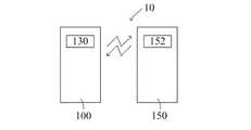
図1は、ワイヤレス制御システムを示す概略図である。 FIG. 1 is a schematic diagram illustrating a wireless control system.
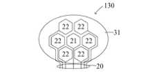
図2は、本発明の実施の形態に係る静電容量性の接触検知モジュールの構造を示す概略図である。 FIG. 2 is a schematic diagram showing the structure of the capacitive contact detection module according to the embodiment of the present invention.
図3は、本発明の実施の形態に係るリードフレームを有する静電容量性の接触検知パッド構造を示す概略図である。 FIG. 3 is a schematic view showing a capacitive contact detection pad structure having a lead frame according to an embodiment of the present invention.
図4Aは、本発明の別の実施の形態に係るリードフレームを有する静電容量性の接触検知パッド構造を示す上面図である。 FIG. 4A is a top view showing a capacitive contact sensing pad structure having a lead frame according to another embodiment of the present invention.
図4Bは、図4Aに示す静電容量性の接触検知パッド構造から製造される静電容量性の接触検知モジュールの断面側面図である。 4B is a cross-sectional side view of a capacitive contact detection module manufactured from the capacitive contact detection pad structure shown in FIG. 4A.
図5は、本発明のさらに別の実施の形態に係るLED部を有する静電容量性の接触検知モジュールの側面図である。 FIG. 5 is a side view of a capacitive contact detection module having an LED unit according to still another embodiment of the present invention.
図6は、接触検知モジュールの有する入力装置を示す斜視図である。 FIG. 6 is a perspective view illustrating an input device included in the contact detection module.
図7は、接触検知モジュールを有するキーパッドのボタンを示す概略図である。 FIG. 7 is a schematic diagram showing buttons of a keypad having a touch detection module.
図8A〜8Cは、本発明の更なる実施の形態に係る静電容量性の接触検知パッド構造を示す上面図である。 8A-8C are top views showing capacitive touch sensing pad structures according to further embodiments of the present invention.
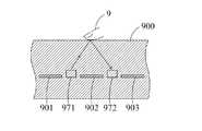
図9は、本発明に係る指紋認証機能を有する接触検知モジュールを示す概略図である。 FIG. 9 is a schematic view showing a contact detection module having a fingerprint authentication function according to the present invention.
本願発明を、以下の形態を参照してより詳細に説明する。以下の本願発明のより好ましい形態の記載は、図面や説明のみの目的のためにここで提供されることに留意されたい。包括的若しくは開示された詳細な形に限定されることを意図したものではない。 The present invention will be described in more detail with reference to the following embodiments. It should be noted that the following description of the more preferred forms of the present invention is provided here for the purpose of drawings and illustration only. It is not intended to be exhaustive or limited to the details disclosed.
図1は、ワイヤレス制御システムを示す概略図である。ワイヤレス制御システム10は、少なくともリモコン100及び被制御装置150を有する。被制御装置150は、リモコン100との間に通信チャンネルを確立するための検知モジュール152を有する。従って、リモコン100は、被制御装置150を制御する制御信号を発する。リモコン100は、さらに、ユーザの接触動作/ジェスチャーを検知、及び検知された接触動作/ジェスチャーを非制御装置150のユーザインタフェース(図示せず)を操作するリモコン信号に変換するための接触検知モジュール130を有する。より詳細には、接触検知モジュール130は静電容量性の接触検知モジュールである。 FIG. 1 is a schematic diagram illustrating a wireless control system. The
静電容量性の接触検知モジュールの構造を図2に示す。静電容量性の接触検知モジュール130は、複数のセンサパッドを有する。本実施の形態において、第1センサパッド21及び第1センサパッドを囲む6個の第2センサパッドがある。センサパッド21,22の形状、数、及び相対位置はこの形態に限定されるものではなく、いかなる適切な変更も本発明に含まれることに留意されたい。センサパッド21及び22の配置は、1次元モードで調節される。センサパッド21及び22は互いに電気的に独立される。各センサパッド21又は22において、静電容量は指のような接触物の接近に伴い変化する。センサパッド21及び22によって生成される電気信号は、それぞれ対応するリード線20を介して処理チップ(図示せず)に伝達される。静電容量性の接触検知モジュール130及び処理チップはラップ31によって覆われ、また保護される。処理チップは、所定操作による接触物の位置/位置変化からユーザの接触動作/ジェスチャーを決定する。このため、センサパッド21及び22近傍のユーザの接触動作/ジェスチャーは、被制御装置150のユーザインタフェースを操作するための制御信号を生成するために検知され得る。詳細な記述は、台湾特許出願201415334号、米国特許出願2014/0097857号及び 2014/0097885号から読み取れ、これらはここでは参照のため組み入れられる。 The structure of the capacitive contact detection module is shown in FIG. The capacitive
1次元の静電容量性の接触検知モジュールの製造方法を容易化する為、リードフレームが使用される。接触検知モジュール130の半ば製品と考えられる接触検知パッド構造が図3に示される。センサパッド21及び22は、それぞれリードフレーム30に接続される。リードフレーム30は、1の主フレーム301及び複数の枝フレーム302を有する。 各々の枝フレーム302は第1端部3021及び第2端部3022を有し、ここで第1端部3021及び第2端部3022は、それぞれ、1のみのセンサパッド(21又は22)及び主フレーム301に接続される。センサパッド21及び22と共にリードフレーム30の主フレーム301及び枝フレーム302は、平面構造を形成し、一体成形の製品を提供するために金属スタンプ処理による容易に製造される。もし狭い線幅が要求されるなら、エッチング法が好ましい。接触検知パッド構造の原料は金属、導電性ポリマー、導電性ゴム、又はスタンプやエッチングで処理できるその他の導電性原料となる。例えば導電性ゴムのような柔軟性原料は、これらの原料からのより好ましい選択となる。他の形態において、接触検知パッド構造は、例えばプラスチック部を金属層で電気メッキするような、非導電性原料を導電性原料で覆うことにより形成される。それから、主フレーム301を除く全体構造は、センサパッド21及び22を固定及び保護するためラップ31で覆われる。実施の形態において、このラッピングの手順は、射出成形により実行され、そしてそれから、主フレーム301が点線に沿って切断され取り除かれる。このようにして、図2の静電容量性の接触検知モジュールが得られる。ラップ31の接触面は平面又は曲面であり、ラップ31は絶縁材で構成される。ラップ31の原料は、透明、半透明又は不透明である。接触検知モジュール130のリード線20(枝フレーム302から形成される)はラップ31から突き出る。リード線20は、リボンケーブル(図示せず)に電気的に接続され、その結果、センサパッド21及び22により生成される電気信号はリード線20及びリボンケーブルを介して他の回路又は構成部に伝達される。従って、接触検知モジュール130と協働する接触制御モジュール(図示せず)は、接触検知モジュール130からの電気信号の所定操作により、検知されたジェスチャー/接触動作を決定するための適切な信号線を介してリード線20に電気的に接続される。 In order to facilitate the manufacturing method of the one-dimensional capacitive contact detection module, a lead frame is used. FIG. 3 shows a contact detection pad structure that can be considered as a half product of the
図4A及び図4Bは本発明の他の形態を示している。この形態において、処理チップ40は、接触検知モジュール130に統合される。処理チップ40を収容するため、第1センサパッド21に窪み部210がある。センサパッド21及び22、リードフレーム30及び処理チップ40は基板41(図4B)上に配置される。リード線20(リード枝302から形成される)は、ワイヤボンディングを介して処理チップ40に電気的に接続され、一方、処理チップ40はまた、ワイヤボンディングを介してピン49に電気的に接続される。基板41は、吸熱器による役目を与えられる。加えて、基板41は、電気ノイズや干渉に対するシールドのためグランド面として機能する金属層(図示せず)を有する場合がある。さらに、駆動電圧は、接触検知モジュール130の感度及び感度距離を向上するため、金属層を介してセンサパッド21及び22上に供給される。上述のように、リードフレーム30は、金属スタンプ処理により一体的に成形される。ラップ31は、主フレーム301を除く全体構造を覆うために形成され、例えば、センサパッド21及び22、枝フレーム302、処理チップ40、及び基板41を覆う。例えば、このラッピングの手順は、射出成形により実行され、そしてそれから、主フレーム301が点線に沿って全構造を切断することで取り除かれる。ラップ31の接触面は平面又は曲面であり、ラップ31は絶縁材で構成される。ラップ31の原料は、透明、半透明又は不透明である。別の形態において、処理チップ40は、センサパッド21及び22の2つの間に配置される。さらに別の形態において、処理チップ40は、センサパッド21及び22の表面の1つの上に配置される。この状況下で、絶縁層(図示せず)は処理チップ40と底にあるセンサパッド21又は22との間に挿入され、若しくは、処理チップ40のピンが底にあるセンサパッド21又は22に電気的に接続される。処理チップ40に加えて、電池、ワイヤレスコミュニケーションチップ、又はリモコン100に必要な他の回路チップが同様の方法で接触検知モジュール130に配置、及び統合される。回路チップはセンサパッド21、22及びリード線20と共にラッピングされる。 4A and 4B show another embodiment of the present invention. In this form, the
本願によると、接触検知モジュールはセンサパッドを限定する。本願の概念は、全体を部分にバラバラとすることである。リモコン100のサイズは、例えばボタンのように、大幅に減らすことができる。従って、本願は他のリモコンより有利な点を得る。さらに、1の接触検知モジュール130が接触検知動作を実行するためにリモコン100に単独で提供され、若しくは複数の接触検知モジュール130が大きな領域の接触検知モジュールを供するために一緒に結合される。その上、複数の小さな接触検知モジュールは柔軟なデザインやアプリケーションを達成するためにリモコン100の異なる箇所に配置される。静電容量性の接触検知モジュール130は、例示として上記形態で記載されているが、全ての形態に他のタイプの接触検知モジュールがまた、例えば、センサパッドが圧力を検知できる圧電性の材料から成る圧電性の接触検知モジュールにも適用可能であることに留意されたい。 According to the present application, the contact detection module defines a sensor pad. The concept of the present application is to separate the whole into parts. The size of the
もしラップ31が透明又は半透明なら、処理チップ40により制御されるLED部はラップ31内に配置される。LED部の輝度及び/又は色は、センサパッド21及び22の接触検知の結果に応じて変化する。すなわち、LED部は検知されたジェスチャー/接触動作に応じて、様々なイルミネーション効果を供する。図5の構造を参照し、ここでは、透明ラップ31が明確化のため省略され、吸熱器が追加的に供される。この構造において、金属層431は上述の形態のセンサパッドに似た方法で形成される。金属層431の大部分は吸熱板43の導電部として機能し、この吸熱板43は、絶縁性のサーマルペースト432によりLED部42に接続される。金属層431の他の部分はセンサパッドとして機能する。センサパッド及びLED部42はワイヤ44により処理チップ40に電気的に接続され、その結果、処理チップ40は、センサパッドの接触検知動作を処理し、LED部42のイルミネーションを制御する。 If the
上述の形態の接触検知モジュールは、例えばコンピュータや他の情報システムの入力装置のように、入力装置の異なるタイプに使用される。図6は、本願に係る接触検知モジュールの有するジョイスティックを示す。ジョイスティック50は基台52及びスティック53を有する。接触検知モジュール51はスティック53の頂上に配置される。ユーザは、スクリーン上のカーソル又は物体の動作を制御するためにスティック53を動かし又は接触検知モジュール51に接触する。より好ましい制御のため、スティック53を動かすことがカーソル又は物体の速い動きになり、一方、接触検知モジュール51を操作することがカーソル又は物体の適当な動きとなる。従って、ユーザはターゲット位置に近くまではカーソルを早く動かすためにスティック53を動かし、そして、それから正確なターゲット位置にカーソルを動かすため、接触検知モジュール51上で指を振り動かし、又は指を通過させる。スティック53及び接触検知モジュール51の処理チップに対応の制御チップ(図示せず)はジョイスティック50に別々に供され、又は実際の適用においては1つのチップに統合される。他の適用では、接触検知モジュール51は運転者/パイロット又は乗客により操作される乗り物又はボートの客室に搭載されるユーザインタフェースとして供される。 The contact detection module of the above-described form is used for different types of input devices, such as an input device of a computer or other information system. FIG. 6 shows a joystick included in the contact detection module according to the present application. The
さらに、本願に係る接触検知モジュールはフローティングタッチを検出できる。従って、接触検知モジュールは、この接触検知モジュールの接触面に平行な指の動作、及び接触検知モジュールに向かう/から離れる指の動作を検出できる。この技術によると、仮想キーが接触検知モジュールの接触面上に形成される。フローティングタッチを検出するため、センサパッドのグループの全静電容量変化が接触面と、ユーザの指、手の平、又はその他の導電性接触物との間の距離を決定するために計算される。センサパッドの数及び検知距離の間には、予め定まった関係がある。例えば、7のセンサパッドは、センサパッドの全静電容量変化を検知することで3のセンサパッドより広い範囲を検知できる。センサパッドのグルーピングに関する詳細な記述は、台湾特許出願201415334号、米国特許出願2014/0097857号及び 2014/0097885号から読み取れ、これらはここで参照のため組み入れられる。静電容量性の接触検知モジュールの検知距離はグルーピングサイズにより決定されるため、連続して変化しているグルーピングサイズは、静電容量性の接触検知モジュールに向かう/から離れるスキャン動作として考えられる。ユーザは、カーソルを、接触検知モジュールを有するパネル上のアイコンに移動するために静電容量性の接触検知モジュールを操作した後、ユーザの指がパネル側に動くとき、静電容量性の接触検知モジュールは押し動作を検知し、押し動作に反応して内側に曲がるなど、アイコンを変形させる。例えば、静電容量性の接触検知モジュールが検知し、パネルとユーザの指との距離が閾値より小さくなると認識すると、アイコンへのアニメーション効果、例えば破裂などが示される。それから、パネルは、アイコンによって示される特定機能を実行する。 Furthermore, the contact detection module according to the present application can detect a floating touch. Therefore, the contact detection module can detect the movement of the finger parallel to the contact surface of the contact detection module and the movement of the finger toward / from the contact detection module. According to this technique, a virtual key is formed on the contact surface of the contact detection module. To detect a floating touch, the total capacitance change of a group of sensor pads is calculated to determine the distance between the contact surface and the user's finger, palm, or other conductive contact. There is a predetermined relationship between the number of sensor pads and the detection distance. For example, the sensor pad 7 can detect a wider range than the sensor pad 3 by detecting a change in the total capacitance of the sensor pad. Detailed descriptions regarding grouping of sensor pads can be read from Taiwan patent application 201415334, US patent applications 2014/0097857 and 2014/0097885, which are hereby incorporated by reference. Since the detection distance of the capacitive contact detection module is determined by the grouping size, the continuously changing grouping size can be considered as a scanning operation toward or away from the capacitive contact detection module. When the user moves the cursor to an icon on the panel with the touch detection module and then operates the capacitive touch detection module, when the user's finger moves to the panel side, the capacitive touch detection The module detects the push action and deforms the icon, such as turning inward in response to the push action. For example, if the capacitive contact detection module detects that the distance between the panel and the user's finger is less than a threshold, an animation effect on the icon, such as a burst, is shown. The panel then performs the specific function indicated by the icon.
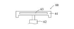
図7はキーパッド又はキーボードのボタンを示す。ボタン60は、キーキャップ61及びキースイッチ62を有し、ここで接触検知モジュール63は、ボタン60のキーキャップ61に配置される。一方、接触検知モジュール63を有するボタン60は、キャラクター又は機能入力を供するために押圧される。他方、接触検知モジュール63を有する1以上のボタン60は、タッチパッドとして機能することができる。接触検知モジュール63は、カーソル又は情報システム上を動く物体を制御するためボタン60上への接触動作を検知する。極座標システムがカーソル又は物体の動作制御において用いられる。例えば、接触検知モジュール63は、固定された中心点に相対する接触位置の距離及び角度を検出する。このようにして、カーソルは、検出された距離及び角度に応じて動くように制御される。カーソルの速度は、距離及び角度に対応する動作方向に比例する。 FIG. 7 shows a keypad or keyboard button. The
再び図1を参照する。被制御装置150の検知モジュール152は、上述した接触検知モジュールにより実行される。接触検知モジュール130の処理チップ40は、外部の制御信号に反応して接触検知モジュール130のセンサパッド21及び22を駆動する異なる電圧信号を発行する。センサパッド21及び22の間の電圧信号分布は、コードとして考えられる。さらに、電圧信号は、時間に伴って電圧信号分布を変えるための高速スイッチング/チェンジング波形を有する。各リモコン100は認識された独自のコードを有する。フローティングタッチ機能を有する検知モジュール152は、対応する検知信号を生成するため接触検知モジュール130及び検知モジュール152間の静電容量変化を検出する。このため、被制御装置150は、通信チャンネルが、リモコン100のコードに対応した静電容量変化を示す検知信号に応じて確立されるべきかを決定できる。このようにして、リモコン100の信頼性が確立される。静電容量性の接触検知機能が説明のために記述されることに留意されたい。実際、接触検知モジュール130及び検知モジュール152は、他の接触検知法を介して信憑性を確認できる。接触検知モジュール130のセンサパッドの物性が特定コードで変化されることのみが要求され、検知モジュール152は物性の変化を検知できる。 Refer to FIG. 1 again. The
この形態において、処理チップ40は、異なる状況で制御信号を受信又は発行する。第1例において、処理チップ40は、接近する接触物から生じるセンサパッドの物性(例えば、静電容量変化)の変化を検知し、指定された構成部(図示せず)を制御する内部制御信号を発行する。第2例において、処理チップ40は、他の制御構成部(図示せず)から外部制御信号を受信する。処理チップ40は、センサパッドを駆動し、外部制御信号に反応する特定のモードで、センサパッドの物性(例えば、静電容量変化)を変化する。 In this form, the
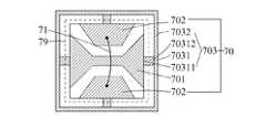
図8Aは、本願に係る静電容量性の接触検知パッド構造を示す上面図である。静電容量性の接触検知パッド構造70は、金属スタンプ処理により製造される。静電容量性の接触検知パッド構造70は、第1センサパッド701、第2センサパッド702及びリードフレーム703を有する。リードフレーム703は、1の主フレーム7032及び複数の枝フレーム7031を有する。各々の枝フレーム7031は、第1端部70311及び第2端部70312を有し、ここで第1端部70311は1のセンサパッド(701又は702)にのみ接続され、第2端部70312は主フレーム7032に接続される。2つの第2センサパッド702はワイヤボンディングを介して電気的に接続される。第1センサパッド701を横切るワイヤ71は、第1センサパッド701から独立される。それから、主フレーム7032を除く静電容量性の接触検知パッド構造70は例えば射出成形によりラップされる。パッド構造70は、静電容量性の接触検知モジュールを得るために、主フレーム7032及び枝フレーム7031の一部を取り除くべく、点線状の正方形79に沿って切断される。複数の静電容量性の接触検知モジュールは、タッチパネルを形成するため所定パターンで連結される。従って、製造過程は接触検知モジュールの適切な量を連結することで、様々なサイズのタッチパネルを柔軟に提供する。 FIG. 8A is a top view showing a capacitive contact detection pad structure according to the present application. The capacitive contact
図8Bは、本願に係る別の静電容量性の接触検知パッド構造を示す。静電容量性の接触検知パッド構造80は、金属スタンプ処理により製造される。静電容量性の接触検知パッド構造80は、第1センサパッド801、第2センサパッド802、パワーパッド808、グランドパッド809、シグナルパッド810及びリードフレーム803を有する。リードフレーム803は、1の主フレーム8032及び複数の枝フレーム8031を有する。各々の枝フレーム8031は、第1端部80311及び第2端部80312を有し、ここで第1端部80311は第1センサパッド801、第2センサパッド802、パワーパッド808、グランドパッド809及びシグナルパッド810に接続され、一方、第2端部80312は主フレーム8032に接続される。点線状の正方形87は、回路チップ870が配置される位置を示す。パワーパッド808、グランドパッド809及びシグナルパッド810はそれぞれワイヤ81,82及び83を介して回路870に電気的に接続され、しかし、本発明は、このような内部接続法に限定されるものではない。それから、静電容量性の接触検知パッド構造80の一部は、例えば射出成形によりラップされる。主フレーム8032及び枝フレーム8031の一部は、埋め込まれた回路チップ870を伴う静電容量性の接触検知モジュールを形成するため切断される。複数の静電容量性の接触検知モジュールは、所定パターンで接続され、ここで埋め込まれた回路チップ870は、例えば、LEDチップ及び/又はセンサチップなど、1以上の回路チップから選択される。本形態では、LEDチップが、シグナルパッド810を介して受信される制御信号により制御される。その代りに、センサチップは、シグナルパッド810を介して検知されるパラメータを発行する。例えば、センサチップは、センサパッド上で用いられる圧力を検知できる圧電センサである。本願は、回路チップ870の位置を限定するものではないことに留意されたい。回路チップ870は、センサパッドの間に配置され、センサパッドの窪み部に配置され、又は絶縁接着材によりパッド801,802,808,809及び810の1の表面上に搭載される。表面は、パッドの上面、裏面又は外側面である。 FIG. 8B shows another capacitive touch sensing pad structure according to the present application. The capacitive contact
図8Cは、本願に係る別の静電容量性の接触検知パッド構造を示す。この構造は、図8Bからシグナルパッド810が取り除かれた構造に似ている。本形態において、外部信号は、第1センサパッド801及び第2センサパッド802を介して受信される。回路チップ870は、ワイヤ86及び85によって第1センサパッド801及び第2センサパッド802に電気的に接続される。このように、時分割多重化(TDM)法を利用することで、第1センサパッド801及び第2センサパッド802は第1時間枠で接触検知動作を実行するために駆動され、回路チップ870の制御は、第2時間枠で実行される。別のケースでは、回路チップ870は、第1センサパッド801又は第2センサパッド802の表面に配置される。この状況下で、絶縁層(図示せず)は回路チップ870と底にあるセンサパッド801又は802との間に挿入され、又は、回路チップ870のピンが底にあるセンサパッド801若しくは802に電気的に接続される。仮に回路チップがLEDチップなら、P型電極又はN型電極がLEDチップの底部で形成され、LEDチップが、ワイヤなしにそれらの間の電気的接続を形成するために第1センサパッド801又は第2センサパッド802上に直接配置される。 FIG. 8C shows another capacitive touch sensing pad structure according to the present application. This structure is similar to the structure in which the
図9は、指紋認証機能を有する接触検知モジュールを示す。この接触検知モジュールにおいて、2つの回路チップ971及び972が、例えば、LEDチップ971及び画像センサチップ972として供される。回路チップ971及び972は、上述のように、例えば、2つのセンサパッドの間に配置、センサパッドの窪み部の中に配置、絶縁接着材により1のセンサパッドの表面上に搭載、又は他の適切な位置に配置される。このため、LEDチップ971及び画像センサチップ972は、保護構造900(例えば、カバーレンズを備え若しくはカバーレンズなしのラップ)に接触する指9の指紋を検知できる。接触検知モジュールが働かないときは、回路チップ971及び972は電力消費を減らすためにオフとなる。一旦センサパッド901,902及び903がユーザの指が保護構造900に接触していることを検知すると、回路チップ971及び972は指紋認証の実行のためオンとなる。指紋認証に通過すると、ユーザは、接触検知モジュール上の更なる接触操作を実行できる。センサパッド901,902及び903、及び回路チップ971及び972は射出成形によりラップされる。保護構造900は透明材料で構成される。これにも関わらず、仮に保護構造900が半透明や不透明なら、貫通孔又は光ガイド構成部が光の伝達を可能にする光道上に供される。 FIG. 9 shows a contact detection module having a fingerprint authentication function. In this contact detection module, two
リードフレーム、センサパッド、吸熱器及び回路チップは、同一面上、又は異なる高さ及び角度で配置される。本願はそれらの相対位置を限定するものではない。レイアウトは異なる要求を満たすために変わる。例えば、LEDチップのイルミネーション表面はリードフレームに直角である。 The lead frame, sensor pad, heat sink and circuit chip are arranged on the same plane or at different heights and angles. The present application does not limit their relative positions. The layout changes to meet different requirements. For example, the illumination surface of the LED chip is perpendicular to the lead frame.
以上のように、本発明に係るワイヤレス制御システム、接触検知モジュール、及び接触検知パッド構造は、リモコン又は接触制御のための広範な要求を満たすことができる。接触検知モジュールのモジュールデザインは、本願の柔軟性及び適用性を高める。このように提案された接触検知パッド構造は、接触検知モジュールの製造方法の単純化を容易にする。 As described above, the wireless control system, the touch detection module, and the touch detection pad structure according to the present invention can satisfy a wide range of requirements for remote control or touch control. The modular design of the contact detection module enhances the flexibility and applicability of the present application. The proposed contact detection pad structure facilitates simplification of the manufacturing method of the contact detection module.
本発明は、最も実際的に好ましい形態となると考えられるものを詳述したが、本発明は上述した形態に限定されるものではない。反対に、修正や似た構造を取り囲むために最も広い解釈に応じた添付の請求項の内容及び範囲以内を含む様々な修正及び似た構造をカバーするように意図されている。 Although the present invention has been described in detail with what is considered to be the most practical preferred form, the present invention is not limited to the form described above. On the contrary, it is intended to cover various modifications and similar structures, including within the content and scope of the appended claims according to their broadest interpretation to enclose the modifications and similar structures.
Claims (17)
Translated fromJapanese第1センサパッドと、
前記第1センサパッドの横に配置された第2センサパッドと、
1の主フレーム及び複数の枝フレームを有し、前記枝フレームの各々が第1端部及び第2端部を有し、前記第1端部は前記第1センサパッド及び前記第2センサパッドの1つに接続され、前記第2端部が前記主フレームに接続される構造のリードフレームと、を備えることを特徴とする接触検知パッド構造。A contact detection pad structure,
A first sensor pad;
A second sensor pad disposed beside the first sensor pad;
One main frame and a plurality of branch frames, each of the branch frames has a first end and a second end, and the first end is formed of the first sensor pad and the second sensor pad. And a lead frame having a structure in which the second end is connected to the main frame.
それぞれ、前記回路チップと前記第1センサパッド及び前記第2センサパッドの1つと電気的に接続された複数のワイヤと、を備えることを特徴とする請求項1記載の接触検知パッド構造。A circuit chip disposed between the first sensor pad and the second sensor pad;
The contact detection pad structure according to claim 1, further comprising: a plurality of wires electrically connected to the circuit chip and one of the first sensor pad and the second sensor pad.
第1センサパッドと、
前記第1センサパッドの横に配置された第2センサパッドと、
前記第1センサパッド及び前記第2センサパッドを覆うラップと、
それぞれ、前記第1センサパッド及び前記第2センサパッドの1つと電気的に接続され、前記第1センサパッド及び前記第2センサパッドにより生成される電気信号を伝送するための前記ラップから突き出た複数のリード線と、を備えることを特徴とする接触検知モジュール。A contact detection module,
A first sensor pad;
A second sensor pad disposed beside the first sensor pad;
A wrap covering the first sensor pad and the second sensor pad;
A plurality of respectively protruding from the wrap for electrically connecting to one of the first sensor pad and the second sensor pad and transmitting an electrical signal generated by the first sensor pad and the second sensor pad A contact detection module.
それぞれ、前記回路チップと前記第1センサパッド及び前記第2センサパッドの1つと電気的に接続された複数のワイヤと、を備え、
前記回路チップ、前記第1センサパッド及び前記第2センサパッドは異なる高さで異なる平面上に配置される、ことを特徴とする請求項5記載の接触検知モジュール。A circuit chip disposed between the first sensor pad and the second sensor pad, or a circuit chip disposed on one of the first sensor pad and the second sensor pad;
A plurality of wires electrically connected to the circuit chip and one of the first sensor pad and the second sensor pad,
The contact detection module according to claim 5, wherein the circuit chip, the first sensor pad, and the second sensor pad are arranged on different planes at different heights.
前記接触検知モジュールは、
複数のセンサパッドと、
前記センサパッドを覆って接触動作を受信するラップと、
前記センサパッドに電気的に接続され、第1例において前記ラップの近くの接触動作から生じる前記センサパッドの物性の変化に反応する内部制御信号を生成し、第2例において外部制御信号に反応して前記センサパッドの物性を変えるため前記センサパッドを駆動する処理チップと、
検知モジュールを有する被制御装置と、を備え、
前記検知モジュールは、前記ラップの背後の前記センサパッドの物性の変化を検知して、センサ信号を生成し、前記被制御装置は、当該センサ信号に反応して制御される、ことを特徴とするワイヤレス制御システム。A wireless control system comprising a contact detection module,
The contact detection module includes:
Multiple sensor pads;
A wrap covering the sensor pad and receiving a contact action;
An internal control signal that is electrically connected to the sensor pad and responds to changes in physical properties of the sensor pad resulting from a contact action near the wrap in the first example, and reacts to an external control signal in the second example. A processing chip for driving the sensor pad to change the physical properties of the sensor pad,
A controlled device having a detection module;
The detection module detects a change in physical properties of the sensor pad behind the lap to generate a sensor signal, and the controlled device is controlled in response to the sensor signal. Wireless control system.
第1センサパッド、第2センサパッド及びリードフレームを形成するステップと、
前記第1センサパッド及び前記第2センサパッドを覆うラップを形成するステップと、
前記接触検知モジュールを形成する主フレームを取り除くステップと、を含み、
ここで、前記リードフレームは、1の主フレーム及び複数の枝フレームを有し、前記枝フレームのそれぞれは第1端部及び第2端部を有し、前記第1端部は前記第1センサパッド及び前記第2センサパッドの1つに接続され、前記第2端部は前記主フレームに接続され、
前記第1センサパッド及び前記第2センサパッドに接続されるリード線は、前記枝フレームから形成され、当該リード線は前記ラップから突き出ている、ことを特徴とする接触検知モジュールの製造方法。A method for manufacturing a contact detection module, comprising:
Forming a first sensor pad, a second sensor pad and a lead frame;
Forming a wrap covering the first sensor pad and the second sensor pad;
Removing a main frame forming the contact detection module;
Here, the lead frame has one main frame and a plurality of branch frames, each of the branch frames has a first end and a second end, and the first end is the first sensor. Connected to one of a pad and the second sensor pad, the second end is connected to the main frame;
A method of manufacturing a contact detection module, wherein a lead wire connected to the first sensor pad and the second sensor pad is formed from the branch frame, and the lead wire protrudes from the wrap.
前記ラップは、射出成形により形成され、
前記主フレームは切断処理により取り除かれる、ことを特徴とする請求項14記載の接触検知モジュールの製造方法。The first sensor pad, the second sensor pad, and the lead frame are integrally formed by a metal stamp process,
The wrap is formed by injection molding,
The method of manufacturing a contact detection module according to claim 14, wherein the main frame is removed by a cutting process.
第1センサパッドと、
前記第1センサパッドの横に配置された第2センサパッドと、
前記第1センサパッド及び前記第2センサパッドの間に配置、又は前記第1センサパッド及び前記第2センサパッドの1つの上に配置された第1回路チップと、
前記第1センサパッド及び前記第2センサパッドの間に配置、又は前記第1センサパッド及び前記第2センサパッドの1つの上に配置された第2回路チップと、
前記第1センサパッド、前記第2センサパッド、前記第1回路チップ、及び前記第2回路チップを覆うラップと、を備え、
前記第1回路チップ及び前記第2回路チップは、前記センサパッドが前記接触検知モジュール上の接触操作を検知するならばオンにされている、ことを特徴とする接触検知モジュール。A contact detection module,
A first sensor pad;
A second sensor pad disposed beside the first sensor pad;
A first circuit chip disposed between the first sensor pad and the second sensor pad, or disposed on one of the first sensor pad and the second sensor pad;
A second circuit chip disposed between the first sensor pad and the second sensor pad, or disposed on one of the first sensor pad and the second sensor pad;
A wrap covering the first sensor pad, the second sensor pad, the first circuit chip, and the second circuit chip,
The contact detection module, wherein the first circuit chip and the second circuit chip are turned on if the sensor pad detects a contact operation on the contact detection module.
Applications Claiming Priority (2)
| Application Number | Priority Date | Filing Date | Title |
|---|---|---|---|
| TW103105166 | 2014-02-17 | ||
| TW103105166 | 2014-02-17 |
Publications (3)
| Publication Number | Publication Date |
|---|---|
| JP2015164038Atrue JP2015164038A (en) | 2015-09-10 |
| JP2015164038A5 JP2015164038A5 (en) | 2018-03-22 |
| JP6539058B2 JP6539058B2 (en) | 2019-07-03 |
Family
ID=53798131
Family Applications (1)
| Application Number | Title | Priority Date | Filing Date |
|---|---|---|---|
| JP2015028523AActiveJP6539058B2 (en) | 2014-02-17 | 2015-02-17 | Wireless control system, touch detection module, and method of manufacturing touch detection module |
Country Status (4)
| Country | Link |
|---|---|
| US (2) | US9760224B2 (en) |
| JP (1) | JP6539058B2 (en) |
| CN (1) | CN104850289B (en) |
| TW (1) | TWI576733B (en) |
Families Citing this family (17)
| Publication number | Priority date | Publication date | Assignee | Title |
|---|---|---|---|---|
| CN104850289B (en)* | 2014-02-17 | 2018-01-09 | 新益先创科技股份有限公司 | Wireless control system, touch sensing electrode integration module, touch sensing module and manufacturing method thereof |
| US10409485B2 (en) | 2014-10-09 | 2019-09-10 | Touchplus Information Corp. | Adaptive user input device |
| KR102325188B1 (en)* | 2015-03-30 | 2021-11-10 | 삼성디스플레이 주식회사 | Touch sensor device |
| CN105260728B (en)* | 2015-11-13 | 2018-08-21 | 杭州指安科技股份有限公司 | A kind of fingerprint capturer adopts finger face uniform induction structure |
| ES2724426T3 (en)* | 2015-11-16 | 2019-09-10 | Srg Global Liria S L U | Plastic molding with perfect integration of man-vehicle interface |
| US10549982B2 (en) | 2016-02-15 | 2020-02-04 | Stmicroelectronics S.R.L. | Pressure sensor encapsulated in elastomeric material, and system including the pressure sensor |
| ITUB20160759A1 (en)* | 2016-02-15 | 2017-08-15 | St Microelectronics Srl | ENCAPSULATED PRESSURE SENSOR IN ELASTOMERIC MATERIAL, AND SYSTEM INCLUDING THE PRESSURE SENSOR |
| KR102698761B1 (en)* | 2016-08-02 | 2024-08-26 | 삼성디스플레이 주식회사 | Touch panel and display device including the same |
| TWI647604B (en)* | 2017-05-31 | 2019-01-11 | 禾瑞亞科技股份有限公司 | Touch human-machine interface device and operation method thereof |
| CN108111892B (en)* | 2017-11-30 | 2020-06-19 | 海信视像科技股份有限公司 | Human-computer interaction method, remote controller and system |
| EP3699737B1 (en)* | 2019-02-25 | 2025-07-30 | Defond Electech Co., Ltd | A control knob with motion sensing for controlling operation of a machine |
| DE102020203034A1 (en) | 2020-03-10 | 2021-09-16 | Siemens Healthcare Gmbh | Hand-operated input device for a medical facility |
| CN114594617A (en)* | 2020-11-20 | 2022-06-07 | 成食科技股份有限公司 | Intelligent glasses |
| CN112699971A (en)* | 2021-03-25 | 2021-04-23 | 荣耀终端有限公司 | Identity authentication method and device |
| TWI801850B (en)* | 2021-04-23 | 2023-05-11 | 凱爾威科技有限公司 | Sensing apparatus and keycap |
| US20240220147A1 (en)* | 2022-12-28 | 2024-07-04 | Western Digital Technologies, Inc. | Storage devices having multi-channel capacitive sensors for detecting gesture based commands |
| CN116069192B (en)* | 2023-03-08 | 2023-06-13 | 上海泰矽微电子有限公司 | Touch positioning method, system and equipment based on multiple touch electrodes |
Citations (5)
| Publication number | Priority date | Publication date | Assignee | Title |
|---|---|---|---|---|
| JPS5257272U (en)* | 1975-10-22 | 1977-04-25 | ||
| JPS6279417A (en)* | 1985-10-03 | 1987-04-11 | Fuji Photo Film Co Ltd | Optical shutter array |
| JPH11132872A (en)* | 1997-11-04 | 1999-05-21 | Nitta Ind Corp | Capacitance-type force detector |
| JP2004191348A (en)* | 2002-05-29 | 2004-07-08 | Nitta Ind Corp | Electrostatic capacity sensor and its manufacturing method |
| JP2012048894A (en)* | 2010-08-25 | 2012-03-08 | Shin Etsu Polymer Co Ltd | Sensor plate and manufacturing method for the same |
Family Cites Families (10)
| Publication number | Priority date | Publication date | Assignee | Title |
|---|---|---|---|---|
| US8111243B2 (en)* | 2006-03-30 | 2012-02-07 | Cypress Semiconductor Corporation | Apparatus and method for recognizing a tap gesture on a touch sensing device |
| WO2010072177A1 (en)* | 2008-12-26 | 2010-07-01 | 联力胜有限公司 | Integrated hand-held wireless keyboard and touch pad apparatus |
| CN102253787B (en)* | 2010-05-21 | 2014-12-10 | 宸鸿科技(厦门)有限公司 | Inductive touch sensor and touch point sensing method thereof |
| TWI435258B (en)* | 2010-07-19 | 2014-04-21 | Tpk Touch Solutions Xiamen Inc | Inductive touch sensor and its detection method |
| CN102981664B (en)* | 2011-09-07 | 2016-10-05 | 宸鸿科技(厦门)有限公司 | Touch electrode structure and the contact panel of application thereof |
| KR101848274B1 (en)* | 2011-09-29 | 2018-04-13 | 주식회사 지2터치 | Touch detecting means, method and touch screen panel using driving back, and display device embedding said the touch screen panel |
| TWI464644B (en)* | 2012-08-03 | 2014-12-11 | Touchplus Information Corp | Touch panel |
| TWI474243B (en) | 2012-10-05 | 2015-02-21 | Touchplus Information Corp | Capacitive touch sensing keyboard |
| US9638731B2 (en) | 2012-10-05 | 2017-05-02 | Touchplus Information Corp. | Capacitive touch keyboard |
| CN104850289B (en)* | 2014-02-17 | 2018-01-09 | 新益先创科技股份有限公司 | Wireless control system, touch sensing electrode integration module, touch sensing module and manufacturing method thereof |
- 2015
- 2015-02-16CNCN201510084339.9Apatent/CN104850289B/enactiveActive
- 2015-02-17USUS14/623,727patent/US9760224B2/enactiveActive
- 2015-02-17JPJP2015028523Apatent/JP6539058B2/enactiveActive
- 2015-02-17TWTW104105476Apatent/TWI576733B/ennot_activeIP Right Cessation
- 2017
- 2017-09-11USUS15/700,464patent/US10042499B2/enactiveActive
Patent Citations (5)
| Publication number | Priority date | Publication date | Assignee | Title |
|---|---|---|---|---|
| JPS5257272U (en)* | 1975-10-22 | 1977-04-25 | ||
| JPS6279417A (en)* | 1985-10-03 | 1987-04-11 | Fuji Photo Film Co Ltd | Optical shutter array |
| JPH11132872A (en)* | 1997-11-04 | 1999-05-21 | Nitta Ind Corp | Capacitance-type force detector |
| JP2004191348A (en)* | 2002-05-29 | 2004-07-08 | Nitta Ind Corp | Electrostatic capacity sensor and its manufacturing method |
| JP2012048894A (en)* | 2010-08-25 | 2012-03-08 | Shin Etsu Polymer Co Ltd | Sensor plate and manufacturing method for the same |
Also Published As
| Publication number | Publication date |
|---|---|
| TWI576733B (en) | 2017-04-01 |
| US9760224B2 (en) | 2017-09-12 |
| TW201533630A (en) | 2015-09-01 |
| US20150234499A1 (en) | 2015-08-20 |
| US20170371456A1 (en) | 2017-12-28 |
| JP6539058B2 (en) | 2019-07-03 |
| CN104850289B (en) | 2018-01-09 |
| CN104850289A (en) | 2015-08-19 |
| US10042499B2 (en) | 2018-08-07 |
Similar Documents
| Publication | Publication Date | Title |
|---|---|---|
| JP6539058B2 (en) | Wireless control system, touch detection module, and method of manufacturing touch detection module | |
| US11747916B2 (en) | Electronic device having multi-functional human interface | |
| EP2350793B1 (en) | Arrangement for a touchscreen and related method of manufacture | |
| EP3631609B1 (en) | Capacitive sensor device | |
| US10804897B2 (en) | Touch-sensitive keypad control device | |
| CN107437045A (en) | Fingerprint identification device and touch device with fingerprint identification function | |
| TWI616824B (en) | Fingerprint recognition device and touch-control device with fingerprint recognition function | |
| JP2015219663A (en) | Keyboard device | |
| KR20230027136A (en) | Electronic device having multi functional human interface and method for controlling the same | |
| KR20170026070A (en) | Touch force sensing apparatus | |
| TWM517397U (en) | Touch display apparatus | |
| JP3182005U (en) | Touch panel | |
| US12111988B1 (en) | Illumination associated with a touch sensitive area | |
| TW201716962A (en) | Touch panel | |
| KR101357797B1 (en) | Super slim touch keyboard | |
| CN106484164B (en) | touch panel | |
| CN205665715U (en) | Fingerprint identification device and touch device with fingerprint identification function | |
| US20140176831A1 (en) | Touch panel | |
| KR101583454B1 (en) | Electronic device comprising touch detection portion formed on main-board | |
| US20250068255A1 (en) | Selective Touch Modes Based on Keyboard Input | |
| US20250068242A1 (en) | Haptics Modes Based on Keyboard Inputs | |
| JP6546778B2 (en) | Touch detection keypad control device | |
| WO2012172167A1 (en) | User input arrangement and related method of manufacture |
Legal Events
| Date | Code | Title | Description |
|---|---|---|---|
| A521 | Request for written amendment filed | Free format text:JAPANESE INTERMEDIATE CODE: A523 Effective date:20180205 | |
| A621 | Written request for application examination | Free format text:JAPANESE INTERMEDIATE CODE: A621 Effective date:20180205 | |
| A977 | Report on retrieval | Free format text:JAPANESE INTERMEDIATE CODE: A971007 Effective date:20181016 | |
| A131 | Notification of reasons for refusal | Free format text:JAPANESE INTERMEDIATE CODE: A131 Effective date:20181120 | |
| A601 | Written request for extension of time | Free format text:JAPANESE INTERMEDIATE CODE: A601 Effective date:20190220 | |
| A521 | Request for written amendment filed | Free format text:JAPANESE INTERMEDIATE CODE: A523 Effective date:20190419 | |
| TRDD | Decision of grant or rejection written | ||
| A01 | Written decision to grant a patent or to grant a registration (utility model) | Free format text:JAPANESE INTERMEDIATE CODE: A01 Effective date:20190514 | |
| A61 | First payment of annual fees (during grant procedure) | Free format text:JAPANESE INTERMEDIATE CODE: A61 Effective date:20190607 | |
| R150 | Certificate of patent or registration of utility model | Ref document number:6539058 Country of ref document:JP Free format text:JAPANESE INTERMEDIATE CODE: R150 | |
| S531 | Written request for registration of change of domicile | Free format text:JAPANESE INTERMEDIATE CODE: R313531 | |
| R250 | Receipt of annual fees | Free format text:JAPANESE INTERMEDIATE CODE: R250 | |
| R350 | Written notification of registration of transfer | Free format text:JAPANESE INTERMEDIATE CODE: R350 | |
| R250 | Receipt of annual fees | Free format text:JAPANESE INTERMEDIATE CODE: R250 | |
| S531 | Written request for registration of change of domicile | Free format text:JAPANESE INTERMEDIATE CODE: R313531 | |
| R350 | Written notification of registration of transfer | Free format text:JAPANESE INTERMEDIATE CODE: R350 | |
| R250 | Receipt of annual fees | Free format text:JAPANESE INTERMEDIATE CODE: R250 | |
| R250 | Receipt of annual fees | Free format text:JAPANESE INTERMEDIATE CODE: R250 |