JP2015149467A - Manufacturing method of thin film transistor substrate - Google Patents
Manufacturing method of thin film transistor substrateDownload PDFInfo
- Publication number
- JP2015149467A JP2015149467AJP2014140843AJP2014140843AJP2015149467AJP 2015149467 AJP2015149467 AJP 2015149467AJP 2014140843 AJP2014140843 AJP 2014140843AJP 2014140843 AJP2014140843 AJP 2014140843AJP 2015149467 AJP2015149467 AJP 2015149467A
- Authority
- JP
- Japan
- Prior art keywords
- layer
- thin film
- film transistor
- substrate
- manufacturing
- Prior art date
- Legal status (The legal status is an assumption and is not a legal conclusion. Google has not performed a legal analysis and makes no representation as to the accuracy of the status listed.)
- Pending
Links
Images


Classifications
- H—ELECTRICITY
- H01—ELECTRIC ELEMENTS
- H01L—SEMICONDUCTOR DEVICES NOT COVERED BY CLASS H10
- H01L21/00—Processes or apparatus adapted for the manufacture or treatment of semiconductor or solid state devices or of parts thereof
- H01L21/02—Manufacture or treatment of semiconductor devices or of parts thereof
- H01L21/04—Manufacture or treatment of semiconductor devices or of parts thereof the devices having potential barriers, e.g. a PN junction, depletion layer or carrier concentration layer
- H01L21/34—Manufacture or treatment of semiconductor devices or of parts thereof the devices having potential barriers, e.g. a PN junction, depletion layer or carrier concentration layer the devices having semiconductor bodies not provided for in groups H01L21/18, H10D48/04 and H10D48/07, with or without impurities, e.g. doping materials
- H01L21/46—Treatment of semiconductor bodies using processes or apparatus not provided for in groups H01L21/428
- H01L21/477—Thermal treatment for modifying the properties of semiconductor bodies, e.g. annealing, sintering
- H—ELECTRICITY
- H10—SEMICONDUCTOR DEVICES; ELECTRIC SOLID-STATE DEVICES NOT OTHERWISE PROVIDED FOR
- H10D—INORGANIC ELECTRIC SEMICONDUCTOR DEVICES
- H10D30/00—Field-effect transistors [FET]
- H10D30/60—Insulated-gate field-effect transistors [IGFET]
- H10D30/67—Thin-film transistors [TFT]
- H10D30/6704—Thin-film transistors [TFT] having supplementary regions or layers in the thin films or in the insulated bulk substrates for controlling properties of the device
- H10D30/6725—Thin-film transistors [TFT] having supplementary regions or layers in the thin films or in the insulated bulk substrates for controlling properties of the device having supplementary regions or layers for improving the flatness of the device
- H—ELECTRICITY
- H10—SEMICONDUCTOR DEVICES; ELECTRIC SOLID-STATE DEVICES NOT OTHERWISE PROVIDED FOR
- H10D—INORGANIC ELECTRIC SEMICONDUCTOR DEVICES
- H10D30/00—Field-effect transistors [FET]
- H10D30/60—Insulated-gate field-effect transistors [IGFET]
- H10D30/67—Thin-film transistors [TFT]
- H10D30/674—Thin-film transistors [TFT] characterised by the active materials
- H10D30/6755—Oxide semiconductors, e.g. zinc oxide, copper aluminium oxide or cadmium stannate
- H10D30/6756—Amorphous oxide semiconductors
- H—ELECTRICITY
- H10—SEMICONDUCTOR DEVICES; ELECTRIC SOLID-STATE DEVICES NOT OTHERWISE PROVIDED FOR
- H10D—INORGANIC ELECTRIC SEMICONDUCTOR DEVICES
- H10D86/00—Integrated devices formed in or on insulating or conducting substrates, e.g. formed in silicon-on-insulator [SOI] substrates or on stainless steel or glass substrates
- H10D86/40—Integrated devices formed in or on insulating or conducting substrates, e.g. formed in silicon-on-insulator [SOI] substrates or on stainless steel or glass substrates characterised by multiple TFTs
- H10D86/421—Integrated devices formed in or on insulating or conducting substrates, e.g. formed in silicon-on-insulator [SOI] substrates or on stainless steel or glass substrates characterised by multiple TFTs having a particular composition, shape or crystalline structure of the active layer
- H10D86/423—Integrated devices formed in or on insulating or conducting substrates, e.g. formed in silicon-on-insulator [SOI] substrates or on stainless steel or glass substrates characterised by multiple TFTs having a particular composition, shape or crystalline structure of the active layer comprising semiconductor materials not belonging to the Group IV, e.g. InGaZnO
- H—ELECTRICITY
- H10—SEMICONDUCTOR DEVICES; ELECTRIC SOLID-STATE DEVICES NOT OTHERWISE PROVIDED FOR
- H10D—INORGANIC ELECTRIC SEMICONDUCTOR DEVICES
- H10D86/00—Integrated devices formed in or on insulating or conducting substrates, e.g. formed in silicon-on-insulator [SOI] substrates or on stainless steel or glass substrates
- H10D86/40—Integrated devices formed in or on insulating or conducting substrates, e.g. formed in silicon-on-insulator [SOI] substrates or on stainless steel or glass substrates characterised by multiple TFTs
- H10D86/451—Integrated devices formed in or on insulating or conducting substrates, e.g. formed in silicon-on-insulator [SOI] substrates or on stainless steel or glass substrates characterised by multiple TFTs characterised by the compositions or shapes of the interlayer dielectrics
- H—ELECTRICITY
- H10—SEMICONDUCTOR DEVICES; ELECTRIC SOLID-STATE DEVICES NOT OTHERWISE PROVIDED FOR
- H10D—INORGANIC ELECTRIC SEMICONDUCTOR DEVICES
- H10D86/00—Integrated devices formed in or on insulating or conducting substrates, e.g. formed in silicon-on-insulator [SOI] substrates or on stainless steel or glass substrates
- H10D86/40—Integrated devices formed in or on insulating or conducting substrates, e.g. formed in silicon-on-insulator [SOI] substrates or on stainless steel or glass substrates characterised by multiple TFTs
- H10D86/60—Integrated devices formed in or on insulating or conducting substrates, e.g. formed in silicon-on-insulator [SOI] substrates or on stainless steel or glass substrates characterised by multiple TFTs wherein the TFTs are in active matrices
- H—ELECTRICITY
- H10—SEMICONDUCTOR DEVICES; ELECTRIC SOLID-STATE DEVICES NOT OTHERWISE PROVIDED FOR
- H10D—INORGANIC ELECTRIC SEMICONDUCTOR DEVICES
- H10D99/00—Subject matter not provided for in other groups of this subclass
Landscapes
- Engineering & Computer Science (AREA)
- Physics & Mathematics (AREA)
- Condensed Matter Physics & Semiconductors (AREA)
- General Physics & Mathematics (AREA)
- Manufacturing & Machinery (AREA)
- Computer Hardware Design (AREA)
- Microelectronics & Electronic Packaging (AREA)
- Power Engineering (AREA)
- Thin Film Transistor (AREA)
- Electroluminescent Light Sources (AREA)
- Electrodes Of Semiconductors (AREA)
- Formation Of Insulating Films (AREA)
Abstract
Description
Translated fromJapanese本開示は、薄膜トランジスタ基板の製造方法に関する。 The present disclosure relates to a method for manufacturing a thin film transistor substrate.
液晶表示装置又は有機EL(Electroluminescense)表示装置などのアクティブマトリクス方式の表示装置には、スイッチング素子又は駆動素子として薄膜トランジスタ(TFT:Thin Film Transistor)が広く用いられている。 Thin film transistors (TFTs) are widely used as switching elements or driving elements in active matrix display devices such as liquid crystal display devices or organic EL (Electroluminescence) display devices.
近年、TFTのチャネル層に酸化亜鉛(ZnO)、酸化インジウムガリウム(InGaO)、又は、酸化インジウムガリウム亜鉛(InGaZnO)などの酸化物半導体を用いた構成について、研究開発が積極的に進められている。例えば、特許文献1には、酸化物半導体を用いたボトムゲート型の薄膜トランジスタが開示されている。酸化物半導体をチャネル層に用いたTFTは、オフ電流が小さく、アモルファス状態でも高いキャリア移動度を持ち、低温プロセスで形成可能であるという特徴を持つ。 In recent years, research and development have been actively conducted on a structure in which an oxide semiconductor such as zinc oxide (ZnO), indium gallium oxide (InGaO), or indium gallium zinc oxide (InGaZnO) is used for a channel layer of a TFT. . For example,
しかしながら、上記従来の薄膜トランジスタでは、ゲート電圧に対するキャリア移動度を示す曲線(以下、「移動度曲線」と記載)において、閾値電圧(具体的には、薄膜トランジスタがオン状態になるゲート−ソース間電圧)付近でピークが発生する場合がある。移動度曲線のピークが発生することにより、薄膜トランジスタの動作が不安定になり、信頼性が低くなる。 However, in the conventional thin film transistor, a threshold voltage (specifically, a gate-source voltage at which the thin film transistor is turned on) in a curve indicating carrier mobility with respect to the gate voltage (hereinafter referred to as “mobility curve”). A peak may occur in the vicinity. When the peak of the mobility curve occurs, the operation of the thin film transistor becomes unstable and the reliability becomes low.
そこで、本開示は、信頼性が高い薄膜トランジスタを備える薄膜トランジスタ基板の製造方法を提供する。 Therefore, the present disclosure provides a method for manufacturing a thin film transistor substrate including a highly reliable thin film transistor.
上記課題を解決するため、本開示の一態様に係る薄膜トランジスタ基板の製造方法は、薄膜トランジスタを備える薄膜トランジスタ基板の製造方法であって、前記薄膜トランジスタの上方に、ポリイミド材料から構成される平坦化層を形成する工程と、前記平坦化層を形成した後に、240℃以下の温度で加熱する工程とを含む。 In order to solve the above problems, a method of manufacturing a thin film transistor substrate according to one embodiment of the present disclosure is a method of manufacturing a thin film transistor substrate including a thin film transistor, and a planarization layer formed of a polyimide material is formed over the thin film transistor. And a step of heating at a temperature of 240 ° C. or lower after forming the planarizing layer.
本開示によれば、信頼性が高い薄膜トランジスタを備える薄膜トランジスタ基板を製造することができる。 According to the present disclosure, a thin film transistor substrate including a highly reliable thin film transistor can be manufactured.
(本開示の概要)
本開示の一態様に係る薄膜トランジスタ基板の製造方法は、薄膜トランジスタを備える薄膜トランジスタ基板の製造方法であって、薄膜トランジスタの上方に、ポリイミド材料から構成される平坦化層を形成する工程と、平坦化層を形成した後に、240℃以下の温度で加熱する工程とを含む。(Outline of this disclosure)
A method of manufacturing a thin film transistor substrate according to one embodiment of the present disclosure is a method of manufacturing a thin film transistor substrate including a thin film transistor, the step of forming a planarization layer made of a polyimide material over the thin film transistor, And a step of heating at a temperature of 240 ° C. or lower after the formation.
これにより、240℃以下の低温の加熱処理を行うことで、移動度曲線のピークの発生を抑制することができる。例えば、平坦化層を形成するまでの工程において高温での加熱処理が行われた場合には、移動度曲線のピークが発生する。この場合であっても、平坦化層を形成した後に240℃以下の低温で加熱処理を行うので、移動度曲線のピークの発生を抑制することができる。したがって、薄膜トランジスタの信頼性を高めることができる。 Thereby, generation | occurrence | production of the peak of a mobility curve can be suppressed by performing low-temperature heat processing of 240 degrees C or less. For example, when heat treatment is performed at a high temperature in the process until the planarization layer is formed, the peak of the mobility curve occurs. Even in this case, since the heat treatment is performed at a low temperature of 240 ° C. or lower after the planarization layer is formed, generation of a peak in the mobility curve can be suppressed. Therefore, the reliability of the thin film transistor can be increased.
また、例えば、本開示の一態様に係る薄膜トランジスタ基板の製造方法では、加熱する工程では、200℃以上の温度で加熱してもよい。 For example, in the method for manufacturing a thin film transistor substrate according to one embodiment of the present disclosure, the heating may be performed at a temperature of 200 ° C. or higher.
これにより、200℃以上、240℃以下の温度で加熱処理を行うことができるので、移動度曲線のピークの発生を適切に抑制することができる。 Thereby, since it can heat-process at the temperature of 200 degreeC or more and 240 degrees C or less, generation | occurrence | production of the peak of a mobility curve can be suppressed appropriately.
また、例えば、本開示の一態様に係る薄膜トランジスタ基板の製造方法では、平坦化層を形成する工程では、ポリイミド材料を成膜した後、250℃以上の温度で加熱することで、平坦化層を形成してもよい。 For example, in the method for manufacturing a thin film transistor substrate according to one embodiment of the present disclosure, in the step of forming the planarization layer, after the polyimide material is formed, the planarization layer is heated at a temperature of 250 ° C. or higher. It may be formed.
これにより、成膜したポリイミド材料を250℃以上の温度で加熱することで、ポリイミド材料の焼き締めを行い、膜質の良い平坦化層を形成することができる。また、平坦化層の焼き締めによって平坦化層からの材料の拡散を抑制し、平坦化層の上方に発光層を形成した場合に、当該発光層の膜質に与える影響を低減することができる。そして、250℃以上の加熱処理によって移動度曲線のピークが発生した薄膜トランジスタに対して低温での加熱処理を行うので、移動度曲線のピークの発生を抑制することができる。 Thus, by heating the formed polyimide material at a temperature of 250 ° C. or higher, the polyimide material can be baked and a planarized layer with good film quality can be formed. Further, when the diffusion of the material from the planarization layer is suppressed by baking the planarization layer and the light emitting layer is formed above the planarization layer, the influence on the film quality of the light emitting layer can be reduced. Then, since the heat treatment at a low temperature is performed on the thin film transistor in which the peak of the mobility curve is generated by the heat treatment at 250 ° C. or higher, the generation of the peak of the mobility curve can be suppressed.
また、例えば、本開示の一態様に係る薄膜トランジスタ基板の製造方法では、薄膜トランジスタの製造方法は、さらに、加熱する工程の後に、平坦化層上に画素電極を形成する工程を含んでもよい。 For example, in the method for manufacturing a thin film transistor substrate according to one embodiment of the present disclosure, the method for manufacturing a thin film transistor may further include a step of forming a pixel electrode over the planarization layer after the heating step.
これにより、画素電極を形成する前に加熱処理を行うので、当該加熱処理の後に成膜される有機層などに、当該加熱処理による熱の影響が及ぶのを抑制することができる。 Accordingly, since heat treatment is performed before the pixel electrode is formed, it is possible to suppress the influence of heat due to the heat treatment on an organic layer or the like formed after the heat treatment.
また、例えば、本開示の一態様に係る薄膜トランジスタ基板の製造方法では、薄膜トランジスタの製造方法は、さらに、薄膜トランジスタのソース電極及びドレイン電極の上方に、ソース電極及びドレイン電極の一方に接続された配線層を形成する工程を含み、平坦化層を形成する工程では、配線層の上方に平坦化層を形成してもよい。 For example, in the method for manufacturing a thin film transistor substrate according to one embodiment of the present disclosure, the method for manufacturing a thin film transistor further includes: a wiring layer connected to one of the source electrode and the drain electrode above the source electrode and the drain electrode of the thin film transistor In the step of forming the planarization layer including the step of forming the planarization layer, the planarization layer may be formed above the wiring layer.
これにより、配線層を形成することでレイアウトの自由度を高めることができる。 Thereby, the freedom degree of a layout can be raised by forming a wiring layer.
また、例えば、本開示の一態様に係る薄膜トランジスタ基板の製造方法では、薄膜トランジスタの半導体層は、酸化物半導体であってもよい。 For example, in the method for manufacturing a thin film transistor substrate according to one embodiment of the present disclosure, the semiconductor layer of the thin film transistor may be an oxide semiconductor.
これにより、酸化物半導体をチャネル層として備える薄膜トランジスタは移動度曲線のピークが発生しやすいので、240℃以下の加熱処理を行うことで、移動度曲線のピークの発生を適切に抑制することができる。 Accordingly, since a thin film transistor including an oxide semiconductor as a channel layer easily generates a peak in a mobility curve, the generation of the peak in the mobility curve can be appropriately suppressed by performing heat treatment at 240 ° C. or lower. .
また、例えば、本開示の一態様に係る薄膜トランジスタ基板の製造方法では、酸化物半導体は、透明アモルファス酸化物半導体であってもよい。 For example, in the method for manufacturing a thin film transistor substrate according to one embodiment of the present disclosure, the oxide semiconductor may be a transparent amorphous oxide semiconductor.
以下、薄膜トランジスタ基板及びその製造方法、並びに、薄膜トランジスタ基板を備える表示装置の一実施の形態について、図面を用いて説明する。なお、以下に説明する実施の形態は、いずれも本開示における好ましい一具体例を示すものである。したがって、以下の実施の形態で示される、数値、形状、材料、構成要素、構成要素の配置位置及び接続形態、工程、並びに、工程の順序などは、一例であって本開示を限定する主旨ではない。よって、以下の実施の形態における構成要素のうち、本開示における最上位概念を示す独立請求項に記載されていない構成要素については、任意の構成要素として説明される。 Hereinafter, an embodiment of a thin film transistor substrate, a manufacturing method thereof, and a display device including the thin film transistor substrate will be described with reference to the drawings. Note that each of the embodiments described below shows a preferred specific example in the present disclosure. Accordingly, the numerical values, shapes, materials, components, arrangement positions and connection forms of components, steps, process orders, and the like shown in the following embodiments are merely examples, and are not intended to limit the present disclosure. Absent. Therefore, among the constituent elements in the following embodiments, constituent elements that are not described in the independent claims indicating the highest concept in the present disclosure are described as arbitrary constituent elements.
なお、各図は、模式図であり、必ずしも厳密に図示されたものではない。また、各図において、実質的に同一の構成に対しては同一の符号を付しており、重複する説明は省略又は簡略化する。 Each figure is a schematic diagram and is not necessarily illustrated strictly. Moreover, in each figure, the same code | symbol is attached | subjected to the substantially same structure, The overlapping description is abbreviate | omitted or simplified.
(実施の形態1)
[有機EL表示装置]
まず、本実施の形態に係る有機EL表示装置10の構成について、図1及び図2を用いて説明する。図1は、本実施の形態に係る有機EL表示装置10の一部切り欠き斜視図である。図2は、本実施の形態に係る有機EL表示装置10のピクセルバンクの一例を示す斜視図である。(Embodiment 1)
[Organic EL display device]
First, the configuration of the organic
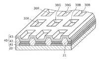
図1に示すように、有機EL表示装置10は、複数個の薄膜トランジスタが配置されたTFT基板(TFTアレイ基板)20と、下部電極である陽極41、有機材料からなる発光層であるEL層42及び透明な上部電極である陰極43からなる有機EL素子(発光部)40との積層構造により構成される。 As shown in FIG. 1, an organic
TFT基板20には複数の画素30がマトリクス状に配置されており、各画素30には画素回路31が設けられている。 A plurality of
有機EL素子40は、複数の画素30のそれぞれに対応して形成されており、各画素30に設けられた画素回路31によって各有機EL素子40の発光の制御が行われる。有機EL素子40は、複数の薄膜トランジスタを覆うように形成された層間絶縁膜(平坦化層)の上に形成される。 The
また、有機EL素子40は、陽極41と陰極43との間にEL層42が配置された構成となっている。陽極41とEL層42との間にはさらに正孔輸送層が積層形成され、EL層42と陰極43との間にはさらに電子輸送層が積層形成されている。なお、陽極41と陰極43との間には、その他の有機機能層が設けられていてもよい。 The
各画素30は、それぞれの画素回路31によって駆動制御される。また、TFT基板20には、画素30の行方向に沿って配置される複数のゲート配線(走査線)50と、ゲート配線50と交差するように画素30の列方向に沿って配置される複数のソース配線(信号配線)60と、ソース配線60と平行に配置される複数の電源配線(図1では省略)とが形成されている。各画素30は、例えば、直交するゲート配線50とソース配線60とによって区画されている。 Each
ゲート配線50は、各画素回路31に含まれるスイッチング素子として動作する薄膜トランジスタのゲート電極と行毎に接続されている。ソース配線60は、各画素回路31に含まれるスイッチング素子として動作する薄膜トランジスタのソース電極と列毎に接続されている。電源配線は、各画素回路31に含まれる駆動素子として動作する薄膜トランジスタのドレイン電極と列毎に接続されている。 The
図2に示すように、有機EL表示装置10の各画素30は、3色(赤色、緑色、青色)のサブ画素30R、30G、30Bによって構成されており、これらのサブ画素30R、30G、30Bは、表示面上に複数個マトリクス状に配列されるように形成されている。各サブ画素30R、30G、30Bは、バンク21によって互いに分離されている。 As shown in FIG. 2, each
バンク21は、ゲート配線50に平行に延びる突条と、ソース配線60に平行に延びる突条とが互いに交差するように、格子状に形成されている。そして、この突条で囲まれる部分(すなわち、バンク21の開口部)の各々とサブ画素30R、30G、30Bの各々とが一対一で対応している。なお、本実施の形態において、バンク21はピクセルバンクとしたが、ラインバンクとしても構わない。 The
陽極41は、TFT基板20上の層間絶縁膜(平坦化層)上でかつバンク21の開口部内に、サブ画素30R、30G、30B毎に形成されている。同様に、EL層42は、陽極41上でかつバンク21の開口部内に、サブ画素30R、30G、30B毎に形成されている。透明な陰極43は、複数のバンク21上で、かつ、全てのEL層42(全てのサブ画素30R、30G、30B)を覆うように、連続的に形成されている。 The
さらに、画素回路31は、各サブ画素30R、30G、30B毎に設けられており、各サブ画素30R、30G、30Bと、対応する画素回路31とは、コンタクトホール及び中継電極によって電気的に接続されている。なお、サブ画素30R、30G、30Bは、EL層42の発光色が異なることを除いて同一の構成である。 Furthermore, the
ここで、画素30における画素回路31の回路構成について、図3を用いて説明する。図3は、本実施の形態に係る有機EL表示装置10における画素回路31の構成を示す電気回路図である。 Here, the circuit configuration of the
図3に示すように、画素回路31は、駆動素子として動作する薄膜トランジスタ32と、スイッチング素子として動作する薄膜トランジスタ33と、対応する画素30に表示するためのデータを記憶するキャパシタ34とで構成される。本実施の形態において、薄膜トランジスタ32は、有機EL素子40を駆動するための駆動トランジスタであり、薄膜トランジスタ33は、画素30を選択するためのスイッチングトランジスタである。 As shown in FIG. 3, the
薄膜トランジスタ32は、薄膜トランジスタ33のドレイン電極33d及びキャパシタ34の一端に接続されるゲート電極32gと、電源配線70に接続されるドレイン電極32dと、キャパシタ34の他端と有機EL素子40の陽極41とに接続されるソース電極32sと、半導体膜(図示せず)とを備える。この薄膜トランジスタ32は、キャパシタ34が保持しているデータ電圧に対応する電流を電源配線70からソース電極32sを通じて有機EL素子40の陽極41に供給する。これにより、有機EL素子40では、陽極41から陰極43へと駆動電流が流れてEL層42が発光する。 The
薄膜トランジスタ33は、ゲート配線50に接続されるゲート電極33gと、ソース配線60に接続されるソース電極33sと、キャパシタ34の一端及び薄膜トランジスタ32のゲート電極32gに接続されるドレイン電極33dと、半導体膜(図示せず)とを備える。この薄膜トランジスタ33は、接続されたゲート配線50及びソース配線60に所定の電圧が印加されると、当該ソース配線60に印加された電圧がデータ電圧としてキャパシタ34に保存される。 The
なお、上記構成の有機EL表示装置10では、ゲート配線50とソース配線60との交点に位置する画素30毎に表示制御を行うアクティブマトリクス方式が採用されている。これにより、各画素30(各サブ画素30R、30G、30B)の薄膜トランジスタ32及び33によって、対応する有機EL素子40が選択的に発光し、所望の画像が表示される。 Note that the organic
[薄膜トランジスタ]
以下では、本実施の形態に係る薄膜トランジスタについて、図4を用いて説明する。なお、本実施の形態に係る薄膜トランジスタは、ボトムゲート型、かつ、チャネル保護型の薄膜トランジスタである。[Thin film transistor]
Hereinafter, the thin film transistor according to this embodiment will be described with reference to FIGS. Note that the thin film transistor according to this embodiment is a bottom-gate and channel protective thin film transistor.
図4は、本実施の形態に係るTFT基板20の概略断面図である。 FIG. 4 is a schematic cross-sectional view of the
図4に示すように、本実施の形態に係るTFT基板20は、基板110と、ゲート電極120と、ゲート絶縁層130と、酸化物半導体層140と、チャネル保護層150と、ソース電極160sと、ドレイン電極160dと、層間絶縁層170と、配線層180と、配線保護層190と、平坦化層200と、画素電極210とを備える。なお、TFT基板20において、薄膜トランジスタ100は、ゲート電極120と、ゲート絶縁層130と、酸化物半導体層140と、チャネル保護層150と、ソース電極160sと、ドレイン電極160dとから構成される。 As shown in FIG. 4, the
薄膜トランジスタ100は、例えば、図3に示す薄膜トランジスタ32である。すなわち、薄膜トランジスタ100は、駆動トランジスタとして利用できる。具体的には、薄膜トランジスタ100が薄膜トランジスタ32(駆動トランジスタ)である場合、ゲート電極120がゲート電極32gに、ソース電極160sがソース電極32sに、ドレイン電極160dがドレイン電極32dに、それぞれ相当する。 The
なお、薄膜トランジスタ100は、例えば、図3に示す薄膜トランジスタ33でもよい。すなわち、薄膜トランジスタ100は、スイッチングトランジスタとして利用してもよい。 The
基板110は、電気絶縁性を有する材料からなる基板である。例えば、基板110は、無アルカリガラス、石英ガラス、高耐熱性ガラスなどのガラス材料、ポリエチレン、ポリプロピレン、ポリイミドなどの樹脂材料、シリコン、ガリウムヒ素などの半導体材料、絶縁層をコーティングしたステンレスなどの金属材料からなる基板である。 The
なお、基板110は、樹脂基板などのフレキシブル基板でもよい。この場合、薄膜トランジスタ100をフレキシブルディスプレイなどに利用することができる。 The
ゲート電極120は、基板110上に所定形状で形成される。ゲート電極120の膜厚は、例えば、20nm〜500nmである。なお、ゲート電極120は、基板110の上方に、例えば、バッファ層などを介して形成されてもよい。 The
ゲート電極120は、導電性を有する材料からなる電極である。例えば、ゲート電極120の材料として、モリブデン、アルミニウム、銅、タングステン、チタン、マンガン、クロム、タンタル、ニオブ、銀、金、プラチナ、パラジウム、インジウム、ニッケル、ネオジムなどの金属、金属の合金、酸化インジウムスズ(ITO)、アルミニウムドープ酸化亜鉛(AZO)、ガリウムドープ酸化亜鉛(GZO)などの導電性金属酸化物、ポリチオフェン、ポリアセチレンなどの導電性高分子などを用いることができる。また、ゲート電極120は、これらの材料を積層した多層構造であってもよい。 The
ゲート絶縁層130は、ゲート電極120と酸化物半導体層140との間に形成される。具体的には、ゲート絶縁層130は、ゲート電極120を覆うようにゲート電極120上及び基板110上に形成される。ゲート絶縁層130の膜厚は、例えば、50nm〜300nmである。 The
ゲート絶縁層130は、電気絶縁性を有する材料から構成される。例えば、ゲート絶縁層130は、シリコン酸化膜、シリコン窒化膜、シリコン酸窒化膜、酸化アルミニウム膜、酸化タンタル膜、酸化ハフニウム膜などの単層膜、又は、これらの積層膜である。 The
酸化物半導体層140は、ゲート電極120に対向するように基板110の上方に形成される。酸化物半導体層140は、薄膜トランジスタ100のチャネル層である。具体的には、酸化物半導体層140は、ゲート電極120に対向する位置に、かつ、ゲート絶縁層130上に形成される。例えば、酸化物半導体層140は、ゲート電極120の上方において、ゲート絶縁層130上に島状に形成される。酸化物半導体層140の膜厚は、例えば、20nm〜200nmである。 The
酸化物半導体層140の材料としては、インジウム(In)、ガリウム(Ga)及び亜鉛(Zn)のうち、少なくとも1種を含む酸化物半導体材料を用いる。例えば、酸化物半導体層140は、アモルファス酸化インジウムガリウム亜鉛(InGaZnO:IGZO)などの透明アモルファス酸化物半導体(TAOS:Transparent Amorphous Oxide Semiconductor)から構成される。 In:Ga:Znの比率は、例えば、約1:1:1である。また、In:Ga:Znの比率は、0.8〜1.2:0.8〜1.2:0.8〜1.2の範囲でもよいが、この範囲には限られない。 As a material of the
なお、チャネル層が透明アモルファス酸化物半導体で構成される薄膜トランジスタは、キャリア移動度が高く、大画面及び高精細の表示装置に適している。また、透明アモルファス酸化物半導体は、低温成膜が可能であるため、プラスチック又はフィルムなどのフレキシブル基板上に容易に形成することができる。 Note that a thin film transistor in which a channel layer is formed using a transparent amorphous oxide semiconductor has high carrier mobility and is suitable for a large-screen and high-definition display device. Further, since the transparent amorphous oxide semiconductor can be formed at a low temperature, it can be easily formed on a flexible substrate such as a plastic or a film.
チャネル保護層150は、酸化物半導体層140上に形成される。例えば、チャネル保護層150は、酸化物半導体層140を覆うように、酸化物半導体層140上、及び、ゲート絶縁層130上に形成される。チャネル保護層150は、酸化物半導体層140を保護する保護層である。チャネル保護層150の膜厚は、例えば、50nm〜500nmである。 The channel
チャネル保護層150は、電気絶縁性を有する材料から構成される。例えば、チャネル保護層150は、シリコン酸化膜、シリコン窒化膜、シリコン酸窒化膜、酸化アルミニウム膜などの無機材料から構成される膜、又は、シリコン、酸素及びカーボンを含む無機材料から構成される膜などの単層膜、又は、これらの積層膜である。 The channel
また、チャネル保護層150の一部は、貫通するように開口されている。つまり、チャネル保護層150には、酸化物半導体層140の一部を露出させるためのコンタクトホール151及び152が形成されている。 A part of the channel
コンタクトホール151は、ソース電極160sと酸化物半導体層140とを電気的に接続するために、酸化物半導体層140のソースコンタクト領域を露出させるためのコンタクトホールである。ソース電極160sを構成する材料は、例えば、コンタクトホール151の壁面に沿って、酸化物半導体層140まで達している。あるいは、コンタクトホール151には、ソース電極160sを構成する材料が充填されていてもよい。 The
コンタクトホール152は、ドレイン電極160dと酸化物半導体層140とを電気的に接続するために、酸化物半導体層140のドレインコンタクト領域を露出させるためのコンタクトホールである。ドレイン電極160dを構成する材料は、例えば、コンタクトホール152の壁面に沿って、酸化物半導体層140まで達している。あるいは、コンタクトホール152には、ドレイン電極160dを構成する材料が充填されていてもよい。 The
ソース電極160s及びドレイン電極160dは、チャネル保護層150上に所定形状で形成される。例えば、ソース電極160s及びドレイン電極160dは、チャネル保護層150上に、基板水平方向に離間して対向配置されている。具体的には、ソース電極160s及びドレイン電極160dはそれぞれ、コンタクトホール151又は152を介して酸化物半導体層140に接続されるように、チャネル保護層150上に形成される。ソース電極160s及びドレイン電極160dの膜厚は、例えば、100nm〜500nmである。 The source electrode 160s and the
ソース電極160s及びドレイン電極160dは、導電性を有する材料からなる電極である。ソース電極160s及びドレイン電極160dの材料としては、例えば、ゲート電極120の材料と同一の材料を用いることができる。 The source electrode 160s and the
層間絶縁層170は、チャネル保護層150の上方に形成される。層間絶縁層170は、チャネル保護層150、ソース電極160s及びドレイン電極160d上に形成される。例えば、層間絶縁層170は、ソース電極160s及びドレイン電極160dを覆うように、チャネル保護層150上、ソース電極160s上及びドレイン電極160d上に形成される。層間絶縁層170は、ソース電極160s及びドレイン電極160dを保護する保護層としても機能する。層間絶縁層170の膜厚は、例えば、100nm〜800nmである。 The interlayer insulating
層間絶縁層170は、電気絶縁性を有する材料から構成される。例えば、層間絶縁層170は、シリコン酸化膜、シリコン窒化膜、シリコン酸窒化膜、酸化アルミニウム膜などの無機材料から構成される膜、又は、シリコン、酸素及びカーボンを含む無機材料から構成される膜などの単層膜、又は、これらの積層膜である。 The interlayer insulating
また、層間絶縁層170の一部は、貫通するように開口されている。つまり、層間絶縁層170には、ドレイン電極160dの一部を露出させるためのコンタクトホール171が形成されている。 A part of the interlayer insulating
コンタクトホール171は、配線層180とドレイン電極160dとを電気的に接続するために形成されたコンタクトホールである。配線層180を構成する材料は、例えば、コンタクトホール171の壁面に沿って、ドレイン電極160dまで達している。あるいは、コンタクトホール171には、ドレイン電極160dを構成する材料が充填されていてもよい。 The
配線層180は、ソース電極160s及びドレイン電極160dの上方に所定形状で形成される。配線層180は、ソース電極160s及びドレイン電極160dの一方に接続される。具体的には、配線層180は、コンタクトホール171を介して、ドレイン電極160dに電気的に接続されている。 The
配線層180は、図4に示すように、第1層181、第2層182、第3層183及び第4層184を含む積層構造を有する。 As shown in FIG. 4, the
第1層181は、層間絶縁層170上に所定形状で形成され、ドレイン電極160dに接続される。第1層181は、導電性を有する材料から構成される。例えば、第1層181は、透明導電膜であり、具体的には、酸化インジウムスズ(ITO)から構成される。第1層181の膜厚は、例えば、50nmである。 The
第2層182は、第1層181上に所定形状で形成される。第2層182は、導電性を有する材料から構成される。例えば、第2層182は、モリブデン膜(Mo膜)である。第2層182の膜厚は、例えば、20nmである。 The
第3層183は、第2層182上に所定形状で形成される。第3層183は、導電性を有する材料から構成される。例えば、第3層183は、銅膜(Cu膜)である。第3層183の膜厚は、例えば、375nmである。 The
第4層184は、第3層183上に所定形状で形成される。第4層184は、導電性を有する材料から構成される。例えば、第4層184は、銅マンガン合金膜(CuMn合金膜)である。第4層184の膜厚は、例えば、65nmである。 The
配線保護層190は、配線層180上に形成される。具体的には、配線保護層190は、配線層180を覆うように、配線層180上、及び、層間絶縁層170上に形成される。配線保護層190は、配線層180を保護する保護層である。配線保護層190の膜厚は、例えば、100nmである。 The wiring
配線保護層190は、電気絶縁性を有する材料から構成される。例えば、配線保護層190は、シリコン酸化膜、シリコン窒化膜、シリコン酸窒化膜、酸化アルミニウム膜などの無機材料から構成される膜、又は、シリコン、酸素及びカーボンを含む無機材料から構成される膜などの単層膜、又は、これらの積層膜である。 The wiring
また、配線保護層190の一部は、貫通するように開口されている。つまり、配線保護層190には、配線層180(第4層184)の一部を露出させるためのコンタクトホール191が形成されている。 A part of the wiring
平坦化層200は、薄膜トランジスタ100の上方、すなわち、ソース電極160s及びドレイン電極160dの上方に形成される。具体的には、平坦化層200は、配線保護層190上に形成される。平坦化層200は、薄膜トランジスタ100の上方を平坦化する。つまり、平坦化層200の上面は、平面である。平坦化層200の膜厚は、例えば、4μmである。 The
平坦化層200は、電気絶縁性を有する材料から構成される。平坦化層200は、ポリイミド材料から構成される。例えば、平坦化層200は、感光性を有するポリイミド系の樹脂材料から構成される。 The
また、平坦化層200の一部は、貫通するように開口されている。つまり、平坦化層200には、コンタクトホール191に連続するコンタクトホール201が形成されている。 A part of the
コンタクトホール201及び191は、配線層180と画素電極210とを電気的に接続するために形成されたコンタクトホールである。画素電極210を構成する材料は、例えば、コンタクトホール201及び191の壁面に沿って、配線層180まで達している。あるいは、コンタクトホール201及び191には、画素電極210を構成する材料が充填されていてもよい。 The contact holes 201 and 191 are contact holes formed to electrically connect the
画素電極210は、平坦化層200上に所定形状で形成される。画素電極210は、例えば、薄膜トランジスタ100の上方に形成される有機EL素子の陽極(図1に示す陽極41)である。 The
画素電極210は、導電性を有する材料からなる電極である。画素電極210は、例えば、アルミニウム、銀などの金属などから構成される。 The
なお、本実施の形態に係る有機EL表示装置10は、さらに、平坦化層200の上方に形成された有機発光層を含む有機EL素子40を備える。具体的には、図1に示すように、TFT基板20は、画素電極210上に順に積層された、EL層42(正孔注入層、正孔輸送層、有機発光層、電子輸送層、電子注入層)と、陰極43とを備える。 The organic
[薄膜トランジスタの製造方法]
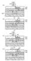
続いて、本実施の形態に係る薄膜トランジスタの製造方法について、図5A〜図5Dを用いて説明する。図5A〜図5Dは、本実施の形態に係るTFT基板20の製造方法を示す概略断面図である。[Thin Film Transistor Manufacturing Method]
Next, a method for manufacturing the thin film transistor according to this embodiment will be described with reference to FIGS. 5A to 5D are schematic cross-sectional views illustrating a method for manufacturing the
まず、図5Aの(a)に示すように、基板110を準備し、基板110の上方に所定形状のゲート電極120を形成する。例えば、基板110上に金属膜をスパッタリングによって成膜し、フォトリソグラフィ及びエッチングによって金属膜を加工することにより、所定形状のゲート電極120を形成する。 First, as shown in FIG. 5A, a
具体的には、まず、基板110としてガラス基板を準備し、基板110上にMo膜とCu膜とをスパッタリングによって順に成膜する。そして、フォトリソグラフィ及びウェットエッチングによってMo膜及びCu膜をパターニングすることにより、ゲート電極120を形成する。なお、Mo膜及びCu膜のウェットエッチングは、例えば、過酸化水素水(H2O2)及び有機酸を混合した薬液を用いることができる。Specifically, first, a glass substrate is prepared as the
次に、図5Aの(b)に示すように、基板110の上方にゲート絶縁層130を形成する。例えば、ゲート電極120を覆うようにゲート絶縁層130をプラズマCVD(Chemical Vapor Deposition)によって成膜する。 Next, as illustrated in FIG. 5A (b), a
具体的には、ゲート電極120を覆うように基板110上にシリコン窒化膜とシリコン酸化膜とをプラズマCVDによって順に成膜することで、ゲート絶縁層130を形成する。シリコン窒化膜は、例えば、シランガス(SiH4)、アンモニアガス(NH3)及び窒素ガス(N2)を導入ガスに用いることで成膜することができる。シリコン酸化膜は、例えば、シランガス(SiH4)と亜酸化窒素ガス(N2O)とを導入ガスに用いることで成膜することができる。Specifically, a
次に、図5Aの(c)に示すように、基板110の上方、かつ、ゲート電極120に対向する位置に所定形状の酸化物半導体層140を形成する。例えば、ゲート絶縁層130上に酸化物半導体膜をスパッタリングによって成膜する。そして、フォトリソグラフィ及びエッチングによって酸化物半導体膜を加工することにより、所定形状の酸化物半導体層140を形成する。 Next, as illustrated in FIG. 5C, an
具体的には、組成比In:Ga:Zn=1:1:1のターゲット材を用いた、酸素(O2)とアルゴン(Ar)との混合ガス雰囲気でのスパッタリングによって、ゲート絶縁層130上にアモルファスInGaZnO膜を成膜する。そして、ゲート絶縁層130上に成膜されたアモルファスInGaZnOをウェットエッチングすることで、酸化物半導体層140を形成する。InGaZnOのウェットエッチングは、例えば、リン酸(H3PO4)、硝酸(HNO3)、酢酸(CH3COOH)及び水を混合した薬液を用いて行うことができる。Specifically, on the
次に、図5Aの(d)に示すように、酸化物半導体層140を覆うようにしてゲート絶縁層130上にチャネル保護層150を形成する。例えば、全面にシリコン酸化膜をプラズマCVDによって成膜することで、チャネル保護層150を形成する。例えば、シリコン酸化膜の膜厚は、50nm〜500nmである。シリコン酸化膜は、例えば、シランガス(SiH4)と亜酸化窒素ガス(N2O)とを導入ガスに用いることで成膜することができる。Next, as illustrated in FIG. 5D, the channel
次に、図5Bの(a)に示すように、チャネル保護層150の一部をエッチング除去することによって、酸化物半導体層140とソース電極160s及びドレイン電極160dとをコンタクトさせるためのコンタクトホール151及び152を形成する。具体的には、酸化物半導体層140の一部が露出するように、フォトリソグラフィ及びエッチングによってコンタクトホール151及び152を形成する。 Next, as shown in FIG. 5B, a part of the channel
例えば、チャネル保護層150がシリコン酸化膜である場合、ドライエッチングとして反応性イオンエッチング(RIE)を用いることができる。このとき、エッチングガスとしては、例えば、四フッ化炭素(CF4)及び酸素ガス(O2)を用いることができる。ガス流量、圧力、印加電力及び周波数などのパラメータは、基板サイズ、エッチングの膜厚などによって適宜設定される。For example, when the channel
次に、図5Bの(b)に示すように、酸化物半導体層140に接続される電極として所定形状のソース電極160s及びドレイン電極160dを形成する。 Next, as illustrated in FIG. 5B, a
具体的には、チャネル保護層150のコンタクトホール151及び152を埋めるようにして、チャネル保護層150上にCu膜をスパッタリングによって成膜する。その後、フォトリソグラフィ及びエッチングによってCu膜を加工することで、所定形状のソース電極160s及びドレイン電極160dを形成する。Cu膜のウェットエッチングは、例えば、過酸化水素水(H2O2)及び有機酸を混合した薬液を用いることができる。Specifically, a Cu film is formed on the channel
次に、図5Bの(c)に示すように、ソース電極160s及びドレイン電極160dを覆うように、層間絶縁層170を成膜する。例えば、200nmのシリコン酸化膜、30nmの酸化アルミニウム膜、200nmのシリコン酸化膜、100nmのシリコン窒化膜を順にスパッタリング及びプラズマCVDによって成膜することで、層間絶縁層170を形成する。 Next, as shown in FIG. 5B (c), an
シリコン酸化膜は、例えば、シランガス(SiH4)と亜酸化窒素ガス(N2O)とを導入ガスに用いたプラズマCVDによって成膜することができる。酸化アルミニウム膜は、例えば、アルミニウムをターゲットに用い、酸素(O2)とアルゴン(Ar)との混合ガス雰囲気でのスパッタリングによって成膜することができる。シリコン窒化膜は、例えば、シランガス(SiH4)、アンモニアガス(NH3)及び窒素ガス(N2)を導入ガスに用いることで成膜することができる。The silicon oxide film can be formed, for example, by plasma CVD using silane gas (SiH4 ) and nitrous oxide gas (N2 O) as introduction gases. The aluminum oxide film can be formed, for example, by sputtering in a mixed gas atmosphere of oxygen (O2 ) and argon (Ar) using aluminum as a target. The silicon nitride film can be formed by using, for example, silane gas (SiH4 ), ammonia gas (NH3 ), and nitrogen gas (N2 ) as the introduction gas.
上層のシリコン窒化膜の成膜後に、例えば、300℃、1時間の条件で加熱処理(アニール)を行う。これにより、酸化物半導体層140を高抵抗化することができる。 After the formation of the upper silicon nitride film, for example, heat treatment (annealing) is performed under the conditions of 300 ° C. and 1 hour. Accordingly, the resistance of the
次に、図5Bの(d)に示すように、層間絶縁層170の一部をエッチング除去することによって、ソース電極160s及びドレイン電極160dの一方が露出するようにコンタクトホール171を形成する。具体的には、ドレイン電極160dの一部が露出するように、フォトリソグラフィ及びエッチングによって層間絶縁層170にコンタクトホール171を形成する。 Next, as shown in FIG. 5D, a part of the interlayer insulating
例えば、シリコン酸化膜及びシリコン窒化膜は、反応性イオンエッチング(RIE)を用いたドライエッチングによってエッチングされる。このとき、エッチングガスとしては、例えば、四フッ化炭素(CF4)及び酸素ガス(O2)を用いることができる。ガス流量、圧力、印加電力及び周波数などのパラメータは、基板サイズ、エッチングの膜厚などによって適宜設定される。For example, the silicon oxide film and the silicon nitride film are etched by dry etching using reactive ion etching (RIE). At this time, for example, carbon tetrafluoride (CF4 ) and oxygen gas (O2 ) can be used as the etching gas. Parameters such as gas flow rate, pressure, applied power, and frequency are appropriately set depending on the substrate size, etching film thickness, and the like.
酸化アルミニウム膜は、例えば、アルカリ性溶液を用いたウェットエッチングによってエッチングされる。酸化アルミニウム膜のウェットエッチングには、例えば、水酸化カリウム(KOH)溶液を用いることができる。 The aluminum oxide film is etched by, for example, wet etching using an alkaline solution. For wet etching of the aluminum oxide film, for example, a potassium hydroxide (KOH) solution can be used.
次に、図5Cの(a)及び(b)に示す手順で、ソース電極160s及びドレイン電極160dの上方に、ソース電極160s及びドレイン電極160dの一方に接続された配線層180を形成する。具体的には、コンタクトホール171を介して露出したドレイン電極160dに接続するように配線層180を形成する。 Next, the
まず、図5Cの(a)に示すように、ソース電極160s及びドレイン電極160dの一方に接続するように、所定形状の第1層181を形成する。具体的には、層間絶縁層170のコンタクトホール171を埋めるようにして、層間絶縁層170上に、スパッタリングによってITO膜を成膜する。その後、フォトリソグラフィ及びエッチングによってITO膜を加工することで、所定形状の第1層181を形成する。ITO膜は、シュウ酸系の薬液を用いたウェットエッチングによってエッチングされる。 First, as illustrated in FIG. 5C, a
第1層181の形成後に、例えば、240℃、30分の条件で加熱処理(ベーク)を行う。これにより、ITO膜を低抵抗化することができる。 After the formation of the
次に、図5Cの(b)に示すように、第1層181上に、所定形状の第2層182、第3層183及び第4層184を順に形成する。具体的には、第1層181を覆うように、Mo膜、Cu膜及びCuMn膜を順にスパッタリングによって成膜する。その後、フォトリソグラフィ及びエッチングによって、Mo膜、Cu膜及びCuMn膜を加工することで、所定形状の第2層182、第3層183及び第4層184を形成する。なお、Mo膜、Cu膜及びCuMn膜は、例えば、過酸化水素水(H2O2)及び有機酸を混合した薬液を用いたウェットエッチングによってエッチングされる。Next, as illustrated in FIG. 5C (b), a
次に、図5Cの(c)に示すように、配線層180を覆うように、配線保護層190を形成する。例えば、100nmのシリコン窒化膜をプラズマCVDによって成膜することで、配線保護層190を形成する。 Next, as shown in FIG. 5C (c), a wiring
配線保護層190の形成後に、例えば、300℃、1時間の条件で加熱処理(アニール)を行う。これにより、酸化物半導体層140を高抵抗化することができる。 After the formation of the wiring
次に、図5Dの(a)に示すように、薄膜トランジスタ100の上方に、ポリイミド材料から構成される平坦化層200を形成する。具体的には、配線層180の上方に平坦化層200を形成する。より具体的には、配線保護層190上に平坦化層200を形成する。例えば、ポリイミド材料から構成される感光性樹脂が配線保護層190上に塗布される。塗布後、例えば、120℃で加熱処理(プリベーク)を行う。 Next, as illustrated in FIG. 5D, a
次に、図5Dの(b)に示すように、平坦化層200の一部を除去することによって、配線保護層190の一部が露出するように、コンタクトホール201を形成する。具体的には、露光及び現像を行うことで、コンタクトホール201を形成する。 Next, as shown in FIG. 5D, a part of the
ポリイミド材料を成膜した後、250℃以上の温度で加熱する。例えば、コンタクトホール201を形成した後、270℃、1時間の条件で加熱処理(ベーク)を行う。これにより、ポリイミド材料の焼き締め、具体的には、残留していた溶剤を揮発させることができる。これにより、平坦化層200が形成される。 After the polyimide material is deposited, it is heated at a temperature of 250 ° C. or higher. For example, after the
次に、図5Dの(c)に示すように、平坦化層200をマスクとして配線保護層190の一部をエッチング除去することで、配線層180(第4層184)の一部が露出するように、コンタクトホール191を形成する。 Next, as shown in FIG. 5D, a part of the wiring
例えば、配線保護層190がシリコン窒化膜である場合、ドライエッチングとして反応性イオンエッチング(RIE)を用いることができる。このとき、エッチングガスとしては、例えば、四フッ化炭素(CF4)及び酸素ガス(O2)を用いることができる。ガス流量、圧力、印加電力及び周波数などのパラメータは、基板サイズ、エッチングの膜厚などによって適宜設定される。For example, when the wiring
本実施の形態では、平坦化層200を形成した後、240℃以下の温度で加熱する工程を含んでいる。具体的には、平坦化層200を形成した後、200℃以上、240℃以下の温度で加熱処理(以下、「低温アニール処理」と記載)を行う。例えば、低温アニール処理は、画素電極210を形成する前に行われる。加熱処理の詳細及びその効果については、後で図8及び図9を用いて説明する。 In this embodiment, after the
次に、図5Dの(d)に示すように、加熱する工程の後に、平坦化層200上に画素電極210を形成する。具体的には、平坦化層200上に、配線層180に接続される所定形状の画素電極210を形成する。画素電極210は、例えば、平坦化層200の上方に形成される有機EL素子の陽極(図に示す陽極41)である。 Next, as illustrated in FIG. 5D, the
具体的には、平坦化層200及び配線保護層190のコンタクトホール201及び191を埋めるようにして、平坦化層200上に、アルミニウム膜(Al膜)をスパッタリングによって成膜する。その後、その後、フォトリソグラフィ及びエッチングによってAl膜を加工することで、所定形状の画素電極210を形成する。Al膜は、例えば、リン酸(H3PO4)、硝酸(HNO3)、酢酸(CH3COOH)及び水を混合した薬液を用いたウェットエッチングによってエッチングされる。Specifically, an aluminum film (Al film) is formed on the
以上のようにして、図4に示すTFT基板20を製造することができる。 As described above, the
なお、平坦化層200の上方には、例えば、有機EL素子(図1に示す有機EL素子40)が形成される。具体的には、画素電極210上に、EL層42(正孔注入層、正孔輸送層、有機発光層、電子輸送層、電子注入層)と、陰極43とが順に積層される。これにより、図1に示す有機EL表示装置10を製造することができる。 For example, an organic EL element (
[キャリア移動度と移動度曲線のピークの有無との関係]
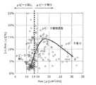
以下では、キャリア移動度μと移動度曲線のピークの有無との関係について、図6及び図7を用いて説明する。[Relationship between carrier mobility and the presence or absence of peaks in the mobility curve]
Hereinafter, the relationship between the carrier mobility μ and the presence or absence of a peak in the mobility curve will be described with reference to FIGS. 6 and 7.
図6は、本実施の形態に係るキャリア移動度の正規確率プロットを示す図である。具体的には、図6は、薄膜トランジスタが複数形成されたTFT基板についての複数のロットを作製し、各薄膜トランジスタのキャリア移動度について基板単位で平均値を求めて作成した正規確率プロットを示している。 FIG. 6 is a diagram showing a normal probability plot of carrier mobility according to the present embodiment. Specifically, FIG. 6 shows a normal probability plot prepared by preparing a plurality of lots for a TFT substrate on which a plurality of thin film transistors are formed, and calculating an average value for each carrier mobility of each thin film transistor. .
ここで、対象とした薄膜トランジスタは、ボトムゲート型、かつ、チャネル保護型であり、アモルファスInGaZnO膜を半導体層として備える。つまり、対象の薄膜トランジスタは、図5A〜図5Dに示した製造方法で作製した薄膜トランジスタ100である。また、ロットは、製造単位を示し、1つのロットは、同時に製造された複数のTFT基板からなる。 Here, the target thin film transistor is a bottom gate type and a channel protection type, and includes an amorphous InGaZnO film as a semiconductor layer. That is, the target thin film transistor is the
図6の縦軸は、キャリア移動度μの平均値(単位:cm2/Vs)を示している。具体的には、キャリア移動度μの平均値は、各薄膜トランジスタに対して、ソース電位Vs=0、ゲート電位Vg=−20V〜+20V、ドレイン電位Vd=4.1Vの条件でドレイン電流Idを測定し、下記の(式1)を用いてキャリア移動度μを算出し、TFT基板毎に平均した値である。The vertical axis in FIG. 6 indicates the average value (unit: cm2 / Vs) of the carrier mobility μ. Specifically, the average value of the carrier mobility μ is the drain current for each thin film transistor under the conditions of the source potential Vs = 0, the gate potential Vg = −20 V to +20 V, and the drain potential Vd = 4.1 V.Id is measured, the carrier mobility μ is calculated using the following (Formula 1), and is an average value for each TFT substrate.

なお、(式1)において、Lは、チャネル長であり、Wは、チャネル幅であり、Coxは、ゲート絶縁層の容量値である。Note that in (Equation 1), L is the channel length, W is the channel width, and Cox is the capacitance value of the gate insulating layer.
図6に示すように、TFT基板毎のキャリア移動度の平均値の分布は、1本の直線状にはならず、直線が途中で上方に折れ曲がった形状となっている。これは、キャリア移動度の平均値が低い領域とキャリア移動度の平均値が高い領域とでは、別の種類の正規分布、すなわち、平均値と標準偏差とが異なる正規分布となっていることを意味する。 As shown in FIG. 6, the distribution of the average value of carrier mobility for each TFT substrate is not a single straight line, but a straight line bent upward in the middle. This is because the regions with low average carrier mobility and regions with high average carrier mobility have different types of normal distributions, that is, normal distributions with different average values and standard deviations. means.
なお、キャリア移動度の平均値が低い側の分布については、破線で示す傾きの小さい直線Aによって近似できる。また、キャリア移動度の平均値が高い側の分布については、実線で示す傾きの大きい直線Bによって近似できる。 Note that the distribution on the side where the average value of the carrier mobility is low can be approximated by a straight line A having a small slope indicated by a broken line. Further, the distribution on the side where the average value of the carrier mobility is higher can be approximated by a straight line B having a large slope shown by a solid line.
ここで、作製されたTFT基板は、以下の(a)〜(c)の3つに分類することができる。 Here, the manufactured TFT substrate can be classified into the following three (a) to (c).
(a)TFT基板内の全ての薄膜トランジスタが移動度曲線のピークを持つもの(以下、「ピーク有基板」と記載する)。 (A) All thin film transistors in a TFT substrate have a peak of a mobility curve (hereinafter referred to as “peaked substrate”).
(b)TFT基板内の全ての薄膜トランジスタが移動度曲線のピークを持たないもの(以下、「ピーク無基板」と記載する)。 (B) All thin film transistors in the TFT substrate do not have a mobility curve peak (hereinafter referred to as “no-peak substrate”).
(c)TFT基板内に、移動度曲線のピークを持つ薄膜トランジスタと、移動度曲線のピークを持たない薄膜トランジスタとが混在しているもの(以下、「混在基板」と記載する)。 (C) A TFT substrate in which a thin film transistor having a mobility curve peak and a thin film transistor having no mobility curve peak are mixed (hereinafter referred to as “mixed substrate”).
図6のプロット結果を用いて、TFT基板の上記(a)〜(c)の分類の対応関係を確認した結果、ピーク有基板をプロットした点は、直線Bに近似される分布に略一致した。また、ピーク無基板をプロットした点は、直線Aに近似される分布に略一致した。そして、混在基板をプロットした点は、これらの分布の中間領域(直線Aの傾き以上、直線Bの傾き以下の領域)における分布に略一致した。これにより、移動度曲線のピークが、キャリア移動度の平均値と標準偏差とを大きくする効果を持つことが分かる。 As a result of confirming the correspondence relationship of the above classifications (a) to (c) of the TFT substrate using the plot result of FIG. 6, the point where the substrate with the peak was plotted substantially matched the distribution approximated to the straight line B. . Further, the points plotted with no peak substrate substantially coincided with the distribution approximated to the straight line A. And the point which plotted the mixed board | substrate substantially matched the distribution in the intermediate area | region (area | region more than the inclination of the straight line A, and below the inclination of the straight line B) of these distributions. This shows that the peak of the mobility curve has the effect of increasing the average value and the standard deviation of the carrier mobility.
このように、ピーク有基板は、直線Bで近似する正規分布を形成し、ピーク無基板は、直線Aで近似する正規分布を形成する。そして、ピーク有基板とピーク無基板とは、中間領域を境にして区別することができる。 In this way, the substrate with peaks forms a normal distribution approximated by a straight line B, and the substrate without peaks forms a normal distribution approximated by a straight line A. A substrate with a peak and a substrate without a peak can be distinguished from each other with an intermediate region as a boundary.
したがって、図6に示すように、プロットした点が直線Aから乖離し始めるキャリア移動度の平均値は、直線Aと直線Bとの交点のキャリア移動度の平均値、具体的には、約13cm2/Vsであることが分かる。つまり、薄膜トランジスタのキャリア移動度が約13cm2/Vs以下であれば、移動度曲線のピークの発生を低減することができる。Therefore, as shown in FIG. 6, the average value of the carrier mobility at which the plotted point starts to deviate from the straight line A is the average value of the carrier mobility at the intersection of the straight line A and the straight line B, specifically about 13 cm.2 / Vs. That is, when the carrier mobility of the thin film transistor is about 13 cm2 / Vs or less, the occurrence of a peak in the mobility curve can be reduced.
図7は、本実施の形態に係るキャリア移動度について、平均値とばらつきとの相関を示す図である。具体的には、図6と同様に、複数のロットを作製し、各薄膜トランジスタのキャリア移動度について基板単位で求めた平均値とばらつきとの相関を示している。 FIG. 7 is a diagram showing the correlation between the average value and the variation for the carrier mobility according to the present embodiment. Specifically, as in FIG. 6, a plurality of lots are prepared, and the correlation between the average value obtained for each substrate and the variation in the carrier mobility of each thin film transistor is shown.
図7の横軸は、TFT基板内の複数の薄膜トランジスタのキャリア移動度の平均値Ave(μ)を示している。また、縦軸は、TFT基板内の複数の薄膜トランジスタのキャリア移動度のばらつきを示している。具体的には、縦軸が示すばらつきの指標として、TFT基板内における複数の薄膜トランジスタのキャリア移動度の標準偏差3σをキャリア移動度の平均値Ave(μ)で割った値を用いた。 The horizontal axis in FIG. 7 indicates the average value Ave (μ) of carrier mobility of a plurality of thin film transistors in the TFT substrate. The vertical axis shows the variation in carrier mobility of a plurality of thin film transistors in the TFT substrate. Specifically, a value obtained by dividing the standard deviation 3σ of the carrier mobility of a plurality of thin film transistors in the TFT substrate by the average value Ave (μ) of the carrier mobility was used as an index of variation indicated by the vertical axis.
ここで、図6を用いて説明したように、移動度曲線のピークの有無は、キャリア移動度の平均値が約13cm2/Vsである場合(図7の太破線)を境にして判別することができる。Here, as described with reference to FIG. 6, the presence / absence of a peak in the mobility curve is discriminated when the average value of carrier mobility is about 13 cm2 / Vs (thick broken line in FIG. 7). be able to.
また、図7に示す太実線の矢印は、分布の近似曲線である。この矢印が示すように、キャリア移動度の平均値が約20cm2/Vsまでの範囲においては、キャリア移動度の平均値とばらつきとは正の相関関係を有する。Moreover, the thick solid line arrow shown in FIG. 7 is an approximate curve of the distribution. As shown by this arrow, in the range where the average value of carrier mobility is up to about 20 cm2 / Vs, the average value of carrier mobility and variation have a positive correlation.
したがって、薄膜トランジスタのキャリア移動度が約13cm2/Vs以下であれば、TFT基板内の薄膜トランジスタ間のキャリア移動度のばらつきを低減することができる。Therefore, if the carrier mobility of the thin film transistor is about 13 cm2 / Vs or less, variation in carrier mobility between the thin film transistors in the TFT substrate can be reduced.
以上のように、本実施の形態に係る薄膜トランジスタでは、キャリア移動度が約13cm2/Vs以下であれば、移動度曲線のピークの発生を低減することができ、かつ、TFT基板内でのキャリア移動度のばらつきを低減することができる。As described above, in the thin film transistor according to this embodiment, when the carrier mobility is about 13 cm2 / Vs or less, the occurrence of a peak in the mobility curve can be reduced, and carriers in the TFT substrate can be reduced. Variation in mobility can be reduced.
[アニール温度とキャリア移動度との関係]
続いて、アニール温度とキャリア移動度との関係について、説明する。[Relationship between annealing temperature and carrier mobility]
Next, the relationship between the annealing temperature and the carrier mobility will be described.
上述したように、本実施の形態では、平坦化層200を形成した後、240℃以下の温度で加熱を行う。これにより、キャリア移動度を約13cm2/Vs以下に低減することができ、移動度曲線のピークの発生を低減することができる。このことについて、以下では、図8及び図9を用いて、薄膜トランジスタのキャリア移動度の測定結果に基づいて説明する。As described above, in this embodiment, after the
図8は、本実施の形態に係る薄膜トランジスタ基板の製造方法における加熱温度の一例を示す図である。図9は、本実施の形態に係る加熱工程と移動度曲線のピークとの関係を示す図である。 FIG. 8 is a diagram showing an example of the heating temperature in the method for manufacturing the thin film transistor substrate according to the present embodiment. FIG. 9 is a diagram showing the relationship between the heating step and the peak of the mobility curve according to the present embodiment.
図9の横軸は、加熱温度を示している。縦軸は、キャリア移動度μのゲート電位(ゲート−ソース間電圧)Vgに対する微分値、すなわち、移動度曲線の傾きを示している。The horizontal axis in FIG. 9 indicates the heating temperature. The vertical axis represents the differential value of the carrier mobility μ with respect to the gate potential (gate-source voltage) Vg , that is, the slope of the mobility curve.
図9は、図8に示す加熱処理を行った後のキャリア移動度を測定し、測定結果に基づいて加熱温度毎にプロットしたものである。具体的には、加熱温度毎にプロットした1つの点は、1つのTFT基板内の複数の薄膜トランジスタのキャリア移動度のそれぞれに対応する。また、図8に示す工程順序(1)〜(8)と、図9に示す(1)〜(8)とは対応している。 FIG. 9 shows the carrier mobility after the heat treatment shown in FIG. 8 is measured and plotted for each heating temperature based on the measurement result. Specifically, one point plotted for each heating temperature corresponds to each of carrier mobility of a plurality of thin film transistors in one TFT substrate. Moreover, process order (1)-(8) shown in FIG. 8 and (1)-(8) shown in FIG. 9 respond | correspond.
図9に太実線で示される直線Cは、キャリア移動度が約13cm2/Vsに相当する直線である。直線Cより上方にプロットされた場合は、移動度曲線のピークが発生することを意味し、直線Cより下方にプロットされた場合は、移動度曲線のピークの発生が抑制されることを意味する。A straight line C indicated by a thick solid line in FIG. 9 is a straight line corresponding to a carrier mobility of approximately 13 cm2 / Vs. When plotted above the straight line C, it means that the peak of the mobility curve occurs, and when plotted below the straight line C, it means that the peak of the mobility curve is suppressed. .
本実施の形態では、図8に示すように、層間絶縁層170、配線層180、配線保護層190及び平坦化層200のそれぞれを形成する工程において、所定の温度、所定の時間の条件で加熱処理を行う。 In this embodiment mode, as shown in FIG. 8, in the step of forming each of the interlayer insulating
まず、図5Bの(c)に示すように層間絶縁層170を成膜した後に、300℃、1時間の条件でアニール処理を行っている(図8の(1))。このとき、キャリア移動度は、約13cm2/Vsより大きくなり、図9の(1)に示すように、プロット結果は、直線Cより上方に位置する。First, as shown in FIG. 5B (c), after the interlayer insulating
次に、図5Cの(a)に示すように配線層180の第1層181(ITO膜)を形成した後に、240℃、30分の条件でベーク処理を行っている(図8の(2))。このとき、キャリア移動度は約13cm2/Vsより小さくなり、図9の(2)に示すように、プロット結果は、直線Cより下方に位置する。Next, as shown in FIG. 5C (a), after the first layer 181 (ITO film) of the
次に、図5Cの(c)に示すように配線保護層190を成膜した後に、300℃、1時間の条件でアニール処理を行っている(図8の(3))。このとき、キャリア移動度は約13cm2/Vsより大きくなり、図9の(3)に示すように、プロット結果は、直線Cより上方に位置する。Next, as shown in FIG. 5C (c), after forming the wiring
以上の3回の加熱処理と測定結果とに基づいて、キャリア移動度の変化が可逆的に行われることが分かる。 It can be seen that the change in carrier mobility is reversibly performed based on the above three heat treatments and the measurement results.
すなわち、低温で加熱処理を行うことでキャリア移動度が約13cm2/Vsより小さくなった薄膜トランジスタを、高温で加熱することで、キャリア移動度を約13cm2/Vsより大きくすることができる。また、高温で加熱処理を行うことでキャリア移動度が約13cm2/Vsより大きくなった薄膜トランジスタを、低温で加熱することで、再びキャリア移動度を約13cm2/Vsより小さくすることができる。That is, a thin film transistor carrier mobility by heat treatment at low temperatures is smaller than about
このように、相対的に高温で加熱処理を行った場合に、キャリア移動度は約13cm2/Vsより大きくなり、移動度曲線のピークが発生する。一方で、相対的に低温で加熱処理を行った場合に、キャリア移動度は約13cm2/Vsより小さくなり、移動度曲線のピークの発生が抑制される。As described above, when heat treatment is performed at a relatively high temperature, the carrier mobility becomes larger than about 13 cm2 / Vs, and the peak of the mobility curve is generated. On the other hand, when heat treatment is performed at a relatively low temperature, the carrier mobility becomes smaller than about 13 cm2 / Vs, and the occurrence of a peak in the mobility curve is suppressed.
したがって、移動度曲線のピークを抑制するためには、最終的に低温での加熱処理、すなわち、低温アニール処理(「追加アニール処理」ともいう)を行えばよいことが分かる。 Therefore, it can be seen that in order to suppress the peak of the mobility curve, heat treatment at a low temperature, that is, low-temperature annealing treatment (also referred to as “addition annealing treatment”) may be finally performed.
追加アニール処理を行うことで、酸化物半導体層140のバックチャネル側の界面に存在する酸素欠陥を補間することができる。これにより、キャリア密度を下げて、移動度曲線のピークの発生が抑制される。 By performing the additional annealing treatment, oxygen defects existing at the interface on the back channel side of the
したがって、酸化物半導体層140上に成膜される層の合計膜厚が大きくなればなるほど、追加アニール処理による移動度曲線のピークの抑制という効果が弱くなる。このため、追加アニール処理は、平坦化層の形成直後であることが好ましい。 Therefore, as the total thickness of the layers formed over the
したがって、本実施の形態では、図5Dの(b)に示すように平坦化層200を形成した後に、270℃、1時間の条件で加熱処理を行う(図8の(4))。これは、上述したように、ポリイミド材料から構成される平坦化層200の焼き締めを行い、膜質の良い平坦化層を形成するための工程である。 Therefore, in this embodiment, after the
この工程により、図9の(4)に示すように、プロット結果は、直線Cより上方に位置し、キャリア移動度は約13cm2/Vsより大きく、移動度曲線のピークが発生する。したがって、平坦化層200を形成する工程の後、具体的には、ポリイミド材料を成膜した後に行う250℃以上の温度での加熱する工程の後に、低温での加熱工程を行うことで、キャリア移動度を小さくし、移動度曲線のピークの発生を低減させる。本実施の形態では、例えば、図5Dの(c)に示すように配線保護層190のコンタクトホール191を形成した後に、低温での加熱処理を行う。By this step, as shown in (4) of FIG. 9, the plot result is located above the straight line C, the carrier mobility is larger than about 13 cm2 / Vs, and the peak of the mobility curve is generated. Accordingly, after the step of forming the
以下では、平坦化層200を形成する工程の後に行う加熱処理の適切な温度を知るために、図8の(5)〜(8)に示す工程を行った。なお、図8の(5)〜(8)に示す工程は、順次行われた工程であり、各工程の間に300℃、1時間の条件でキャリア移動度を約13cm2/Vsより大きくする工程を挟んでいる。つまり、図8の(5)〜(8)に示す工程のそれぞれを開始する時点では、対象となる薄膜トランジスタは、移動度曲線のピークが発生する状態にされている。Below, in order to know the suitable temperature of the heat processing performed after the process of forming the
図9の(5)及び(6)に示すように、加熱処理の温度が230℃及び200℃の場合は、キャリア移動度が約13cm2/Vsより小さくなり、プロット結果は、直線Cより下方に位置する。一方で、図9の(7)及び(8)に示すように、加熱処理の温度が260℃及び250どの場合は、キャリア移動度が約13cm2/Vsより大きくなり、プロット結果は、直線Cより上方に位置する。As shown in (5) and (6) of FIG. 9, when the heat treatment temperature is 230 ° C. and 200 ° C., the carrier mobility is smaller than about 13 cm2 / Vs, and the plot result is lower than the straight line C. Located in. On the other hand, as shown in (7) and (8) of FIG. 9, when the temperature of the heat treatment is 260 ° C. or 250, the carrier mobility becomes larger than about 13 cm2 / Vs, and the plotted result is a straight line C Located above.
図9の(1)〜(8)に示すプロット結果の近似曲線が、曲線Dである。曲線Dと直線Cとの交点は、図9に示すように、約245℃である。つまり、最終的な低温での加熱処理は、245℃以下、好ましくは、240℃以下で行われる。 The approximate curve of the plot results shown in (1) to (8) of FIG. The intersection of the curve D and the straight line C is about 245 ° C. as shown in FIG. That is, the final heat treatment at a low temperature is performed at 245 ° C. or lower, preferably 240 ° C. or lower.
また、図9の(6)に示すように、200℃で加熱した場合も、キャリア移動度は約13cm2/Vsより小さく、移動度曲線のピークの発生が抑制される。したがって、加熱処理は、少なくとも200℃以上で行った場合には、移動度曲線のピークの発生が抑制されることが分かる。Further, as shown in (6) of FIG. 9, even when heated at 200 ° C., the carrier mobility is smaller than about 13 cm2 / Vs, and the occurrence of the peak of the mobility curve is suppressed. Therefore, it can be seen that when the heat treatment is performed at least at 200 ° C. or higher, the peak of the mobility curve is suppressed.
[まとめ]
以上のことから、本実施の形態に係るTFT基板20は、例えば、図10に示すフローチャートに従って製造することができる。図10は、本実施の形態に係るTFT基板20の製造方法を示すフローチャートである。[Summary]
From the above, the
本実施の形態では、図5A〜図5Cで説明したように、まず、薄膜トランジスタ100を形成する(S10)。次に、薄膜トランジスタ100の上方に平坦化層200を形成する(S20)。 In the present embodiment, as described with reference to FIGS. 5A to 5C, first, the
平坦化層200を形成した後、薄膜トランジスタ100の低温アニール処理を行う(S30)。具体的には、200℃以上240℃以下の温度で、薄膜トランジスタ100をアニールする。そして、低温アニール処理の後、平坦化層200上に、有機EL素子の画素電極210を形成する(S40)。 After the
このように、本実施の形態では、薄膜トランジスタ100の低温アニール処理を、平坦化層200の形成後、有機EL素子を構成する複数の層のいずれかを形成する前に行う。具体的には、低温アニール処理は、図10に示すように、画素電極210の形成前に行われる。言い換えると、低温アニール処理は、平坦化層200の形成直後に行われる。 As described above, in this embodiment, the low-temperature annealing treatment of the
以上のように、本実施の形態に係るTFT基板20の製造方法は、薄膜トランジスタ100を備えるTFT基板20の製造方法であって、薄膜トランジスタ100の上方に、ポリイミド材料から構成される平坦化層200を形成する工程と、平坦化層200を形成した後に、240℃以下の温度で加熱する工程とを含む。 As described above, the manufacturing method of the
これにより、240℃以下の低温の加熱処理を行うことで、移動度曲線のピークの発生を抑制することができる。例えば、平坦化層200を形成するまでの工程において高温での加熱処理が行われた場合には、移動度曲線のピークが発生する。この場合であっても、平坦化層200を形成した後に240℃以下の低温で加熱処理を行うので、移動度曲線のピークの発生を抑制することができる。したがって、薄膜トランジスタ100の信頼性を高めることができる。 Thereby, generation | occurrence | production of the peak of a mobility curve can be suppressed by performing low-temperature heat processing of 240 degrees C or less. For example, when heat treatment at a high temperature is performed in the process until the
(他の実施の形態)
以上のように、本出願において開示する技術の例示として、実施の形態を説明した。しかしながら、本開示における技術は、これらに限定されず、適宜、変更、置き換え、付加、省略などを行った実施の形態にも適用可能である。(Other embodiments)
As described above, the embodiments have been described as examples of the technology disclosed in the present application. However, the technology in the present disclosure is not limited to these, and can also be applied to embodiments in which changes, replacements, additions, omissions, and the like are appropriately performed.
例えば、上記実施の形態では、図5Dの(c)に示すようにコンタクトホール191を形成した後で、240℃以下の加熱処理を行ったが、これに限らない。例えば、コンタクトホール191を形成する前、具体的には、図5Dの(b)に示すようにコンタクトホール201を形成した後であって、平坦化層200の焼き締めを行った後に、240℃以下の加熱処理を行ってもよい。 For example, in the above embodiment, after the
また、平坦化層200の直後に低温アニール処理を行う場合に比べてピークの抑制効果は弱まるかもしれないが、画素電極210を形成した後に、240℃以下の加熱処理を行ってもよい。この場合でも、低温アニール処理を行わない場合に比べて、移動度曲線のピークの発生を抑制することができる。 In addition, although the peak suppression effect may be weaker than in the case where the low-temperature annealing process is performed immediately after the
また、TFT基板20は、配線保護層190を備えなくてもよい。例えば、配線層180上に平坦化層200が形成されてもよい。 Further, the
また、上記実施の形態では、配線層180が4層構造である例について示したが、これに限らない。配線層180は、例えば、銅膜などの単層膜でもよい。また、配線層180は、ドレイン電極160dと接続する例について示したが、配線層180は、ソース電極160sと接続されてもよい。 In the above embodiment, an example in which the
また、TFT基板20は、配線層180を備えなくてもよい。例えば、ソース電極160s及びドレイン電極160d上に平坦化層200が形成されてもよい。あるいは、層間絶縁層170上に平坦化層200が形成されてもよい。 Further, the
また、例えば、上記実施の形態において、図5Aの(d)及び図5Bの(a)に示すように、チャネル保護膜(絶縁膜)を全面成膜後に、コンタクトホール151及び152を形成したが、これに限られない。例えば、酸化物半導体層140が露出するように予め所定形状にパターニングされたチャネル保護層150を形成してもよい。 Further, for example, in the above embodiment, as shown in FIG. 5A (d) and FIG. 5B (a), the contact holes 151 and 152 are formed after forming the channel protective film (insulating film) over the entire surface. Not limited to this. For example, the channel
つまり、チャネル保護層150を形成する工程では、酸化物半導体層140の一部が露出するようにチャネル保護層150を形成すればよい。また、ソース電極160s及びドレイン電極160dを形成する工程では、露出した部分で酸化物半導体層140に接続されるようにソース電極160s及びドレイン電極160dを形成すればよい。 That is, in the step of forming the channel
酸化物半導体層140など所定形状にパターニングが必要な層の形成も同様である。すなわち、全面成膜後にパターニングするのではなく、予め所定形状にパターニングされた酸化物半導体層140を形成してもよい。 The same applies to formation of a layer that needs to be patterned into a predetermined shape, such as the
また、上記実施の形態では、酸化物半導体層140に用いる酸化物半導体は、アモルファスのInGaZnOに限られない。例えば、多結晶InGaOなどの多結晶半導体でもよい。 In the above embodiment, the oxide semiconductor used for the
また、上記実施の形態では、薄膜トランジスタ100が酸化物半導体層140を備える構成について説明したが、これに限らない。薄膜トランジスタ100は、単結晶半導体、化合物半導体などの酸化物ではない半導体材料を主成分とする半導体層を備えてもよい。 In the above embodiment, the structure in which the
また、上記実施の形態では、薄膜トランジスタ100がボトムゲート型、かつ、チャネル保護型の薄膜トランジスタである例について説明したが、これに限らない。薄膜トランジスタ100は、ボトムゲート型、かつ、チャネルエッチ型の薄膜トランジスタでもよい。あるいは、薄膜トランジスタ100は、トップゲート型の薄膜トランジスタでもよい。 In the above embodiment, the example in which the
また、上記実施の形態では、薄膜トランジスタ100を用いた表示装置として有機EL表示装置10について説明したが、上記実施の形態における薄膜トランジスタ100は、液晶表示装置など、アクティブマトリクス基板が用いられる他の表示装置にも適用することができる。 In the above embodiment, the organic
また、上述した有機EL表示装置10などの表示装置(表示パネル)については、フラットパネルディスプレイとして利用することができ、テレビジョンセット、パーソナルコンピュータ、携帯電話など、表示パネルを有するあらゆる電子機器に適用することができる。特に、大画面及び高精細の表示装置に適している。 In addition, the display device (display panel) such as the organic
その他、各実施の形態及び変形例に対して当業者が思いつく各種変形を施して得られる形態や、本開示における発明の主旨を逸脱しない範囲で各実施の形態及び変形例における構成要素及び機能を任意に組み合わせることで実現される形態も本開示に含まれる。 In addition, components and functions in each embodiment and modification may be obtained without departing from the gist of the present invention in the form obtained by subjecting each embodiment and modification to various modifications conceived by those skilled in the art. Forms realized by arbitrary combinations are also included in the present disclosure.
本開示に係る薄膜トランジスタ基板の製造方法は、例えば、有機EL表示装置などの表示装置の製造方法などに利用することができる。 The method for manufacturing a thin film transistor substrate according to the present disclosure can be used, for example, for a method for manufacturing a display device such as an organic EL display device.
10 有機EL表示装置
20 TFT基板
21 バンク
30 画素
30B、30G、30R サブ画素
31 画素回路
32、33、100 薄膜トランジスタ
32d、33d、160d ドレイン電極
32g、33g、120 ゲート電極
32s、33s、160s ソース電極
34 キャパシタ
40 有機EL素子
41 陽極
42 EL層
43 陰極
50 ゲート配線
60 ソース配線
70 電源配線
110 基板
130 ゲート絶縁層
140 酸化物半導体層
150 チャネル保護層
151、152、171、191、201 コンタクトホール
170 層間絶縁層
180 配線層
181 第1層
182 第2層
183 第3層
184 第4層
190 配線保護層
200 平坦化層
210 画素電極10 Organic
Claims (7)
Translated fromJapanese前記薄膜トランジスタの上方に、ポリイミド材料から構成される平坦化層を形成する工程と、
前記平坦化層を形成した後に、240℃以下の温度で加熱する工程とを含む
薄膜トランジスタ基板の製造方法。A method of manufacturing a thin film transistor substrate including a thin film transistor,
Forming a planarizing layer made of a polyimide material above the thin film transistor;
And a step of heating at a temperature of 240 ° C. or lower after forming the planarizing layer.
請求項1に記載の薄膜トランジスタ基板の製造方法。The method for manufacturing a thin film transistor substrate according to claim 1, wherein in the heating step, heating is performed at a temperature of 200 ° C. or higher.
請求項1又は2に記載の薄膜トランジスタ基板の製造方法。3. The method of manufacturing a thin film transistor substrate according to claim 1, wherein, in the step of forming the planarization layer, the planarization layer is formed by heating the polyimide material and then heating at a temperature of 250 ° C. or higher. .
前記加熱する工程の後に、前記平坦化層上に画素電極を形成する工程を含む
請求項1〜3のいずれか1項に記載の薄膜トランジスタ基板の製造方法。The method of manufacturing the thin film transistor further includes:
The manufacturing method of the thin-film transistor substrate of any one of Claims 1-3 including the process of forming a pixel electrode on the said planarization layer after the said process to heat.
前記薄膜トランジスタのソース電極及びドレイン電極の上方に、前記ソース電極及び前記ドレイン電極の一方に接続された配線層を形成する工程を含み、
前記平坦化層を形成する工程では、前記配線層の上方に前記平坦化層を形成する
請求項1〜4のいずれか1項に記載の薄膜トランジスタ基板の製造方法。The method of manufacturing the thin film transistor further includes:
Forming a wiring layer connected to one of the source electrode and the drain electrode above the source electrode and the drain electrode of the thin film transistor;
The method for manufacturing a thin film transistor substrate according to claim 1, wherein in the step of forming the planarization layer, the planarization layer is formed above the wiring layer.
請求項1〜5のいずれか1項に記載の薄膜トランジスタ基板の製造方法。The method for manufacturing a thin film transistor substrate according to claim 1, wherein the semiconductor layer of the thin film transistor is an oxide semiconductor.
請求項6に記載の薄膜トランジスタ基板の製造方法。The method for manufacturing a thin film transistor substrate according to claim 6, wherein the oxide semiconductor is a transparent amorphous oxide semiconductor.
Priority Applications (2)
| Application Number | Priority Date | Filing Date | Title |
|---|---|---|---|
| JP2014140843AJP2015149467A (en) | 2014-01-10 | 2014-07-08 | Manufacturing method of thin film transistor substrate |
| US14/580,896US9741588B2 (en) | 2014-01-10 | 2014-12-23 | Method of manufacturing thin-film transistor substrate |
Applications Claiming Priority (3)
| Application Number | Priority Date | Filing Date | Title |
|---|---|---|---|
| JP2014003761 | 2014-01-10 | ||
| JP2014003761 | 2014-01-10 | ||
| JP2014140843AJP2015149467A (en) | 2014-01-10 | 2014-07-08 | Manufacturing method of thin film transistor substrate |
Publications (1)
| Publication Number | Publication Date |
|---|---|
| JP2015149467Atrue JP2015149467A (en) | 2015-08-20 |
Family
ID=53521958
Family Applications (1)
| Application Number | Title | Priority Date | Filing Date |
|---|---|---|---|
| JP2014140843APendingJP2015149467A (en) | 2014-01-10 | 2014-07-08 | Manufacturing method of thin film transistor substrate |
Country Status (2)
| Country | Link |
|---|---|
| US (1) | US9741588B2 (en) |
| JP (1) | JP2015149467A (en) |
Cited By (1)
| Publication number | Priority date | Publication date | Assignee | Title |
|---|---|---|---|---|
| JP2018081903A (en)* | 2016-11-15 | 2018-05-24 | 三星ディスプレイ株式會社Samsung Display Co.,Ltd. | Organic light-emitting display device and manufacturing method thereof |
Families Citing this family (6)
| Publication number | Priority date | Publication date | Assignee | Title |
|---|---|---|---|---|
| US9799772B2 (en)* | 2013-05-29 | 2017-10-24 | Joled Inc. | Thin film transistor device, method for manufacturing same and display device |
| KR102366421B1 (en)* | 2015-07-29 | 2022-02-23 | 엘지디스플레이 주식회사 | Backplate for foldable display device and foldable display device including the same |
| CN106292104B (en)* | 2016-08-30 | 2018-12-25 | 深圳市华星光电技术有限公司 | Array substrate and preparation method thereof, liquid crystal display panel |
| WO2019003305A1 (en)* | 2017-06-27 | 2019-01-03 | 堺ディスプレイプロダクト株式会社 | Organic el device production method |
| CN107221610B (en)* | 2017-07-25 | 2019-03-12 | 南京迈智芯微光电科技有限公司 | One kind proposing high performance silicon-based organic light-emitting device and its manufacturing method |
| CN111799280A (en)* | 2020-07-20 | 2020-10-20 | 京东方科技集团股份有限公司 | Display substrate and preparation method thereof, and display device |
Citations (5)
| Publication number | Priority date | Publication date | Assignee | Title |
|---|---|---|---|---|
| JP2011077514A (en)* | 2009-09-04 | 2011-04-14 | Semiconductor Energy Lab Co Ltd | Method of manufacturing semiconductor device |
| WO2011135908A1 (en)* | 2010-04-30 | 2011-11-03 | シャープ株式会社 | Circuit board and display device |
| JP2011222780A (en)* | 2010-04-09 | 2011-11-04 | Dainippon Printing Co Ltd | Thin film transistor substrate and method of manufacturing thin film transistor |
| JP2013110394A (en)* | 2011-10-24 | 2013-06-06 | Semiconductor Energy Lab Co Ltd | Semiconductor device and method for manufacturing semiconductor device |
| JP2013201440A (en)* | 2009-10-08 | 2013-10-03 | Semiconductor Energy Lab Co Ltd | Semiconductor device |
Family Cites Families (5)
| Publication number | Priority date | Publication date | Assignee | Title |
|---|---|---|---|---|
| KR101146574B1 (en) | 2006-12-05 | 2012-05-16 | 캐논 가부시끼가이샤 | Method for manufacturing thin film transistor using oxide semiconductor and display apparatus |
| JP5305630B2 (en) | 2006-12-05 | 2013-10-02 | キヤノン株式会社 | Manufacturing method of bottom gate type thin film transistor and manufacturing method of display device |
| WO2011126076A1 (en)* | 2010-04-09 | 2011-10-13 | 大日本印刷株式会社 | Thin-film transistor substrate |
| JP5735506B2 (en) | 2010-06-29 | 2015-06-17 | 株式会社Joled | Manufacturing method of organic light emitting device |
| KR102042483B1 (en)* | 2012-09-24 | 2019-11-12 | 한국전자통신연구원 | Thin film transistor and forming the same |
- 2014
- 2014-07-08JPJP2014140843Apatent/JP2015149467A/enactivePending
- 2014-12-23USUS14/580,896patent/US9741588B2/enactiveActive
Patent Citations (5)
| Publication number | Priority date | Publication date | Assignee | Title |
|---|---|---|---|---|
| JP2011077514A (en)* | 2009-09-04 | 2011-04-14 | Semiconductor Energy Lab Co Ltd | Method of manufacturing semiconductor device |
| JP2013201440A (en)* | 2009-10-08 | 2013-10-03 | Semiconductor Energy Lab Co Ltd | Semiconductor device |
| JP2011222780A (en)* | 2010-04-09 | 2011-11-04 | Dainippon Printing Co Ltd | Thin film transistor substrate and method of manufacturing thin film transistor |
| WO2011135908A1 (en)* | 2010-04-30 | 2011-11-03 | シャープ株式会社 | Circuit board and display device |
| JP2013110394A (en)* | 2011-10-24 | 2013-06-06 | Semiconductor Energy Lab Co Ltd | Semiconductor device and method for manufacturing semiconductor device |
Cited By (2)
| Publication number | Priority date | Publication date | Assignee | Title |
|---|---|---|---|---|
| JP2018081903A (en)* | 2016-11-15 | 2018-05-24 | 三星ディスプレイ株式會社Samsung Display Co.,Ltd. | Organic light-emitting display device and manufacturing method thereof |
| JP7063548B2 (en) | 2016-11-15 | 2022-05-09 | 三星ディスプレイ株式會社 | Organic light emission display device and its manufacturing method |
Also Published As
| Publication number | Publication date |
|---|---|
| US9741588B2 (en) | 2017-08-22 |
| US20150200113A1 (en) | 2015-07-16 |
Similar Documents
| Publication | Publication Date | Title |
|---|---|---|
| TWI615983B (en) | Thin film transistor array substrate and manufacturing method thereof | |
| JP6358596B2 (en) | Method for manufacturing thin film transistor substrate | |
| CN102148258B (en) | Thin film transistor, method of manufacturing thin film transistor, display unit, and electronic device | |
| JP6311899B2 (en) | Thin film transistor substrate and manufacturing method thereof | |
| JP2015149467A (en) | Manufacturing method of thin film transistor substrate | |
| JPWO2016056204A1 (en) | THIN FILM TRANSISTOR SUBSTRATE, METHOD FOR PRODUCING THIN FILM TRANSISTOR SUBSTRATE, AND DISPLAY PANEL | |
| JP2010182818A (en) | Thin-film transistor, and display device | |
| US20160163868A1 (en) | Thin-film transistor, method of fabricating thin-film transistor, and display device | |
| JP2010182819A (en) | Thin-film transistor, and display device | |
| JP6142200B2 (en) | Thin film semiconductor device and manufacturing method thereof | |
| JPWO2012137251A1 (en) | Thin film semiconductor device for display device and manufacturing method thereof | |
| JP2016111105A (en) | Thin film transistor, manufacturing method thereof, and display device | |
| JP6142300B2 (en) | Thin film transistor manufacturing method | |
| US9627515B2 (en) | Method of manufacturing thin-film transistor substrate | |
| US9595601B2 (en) | Method of fabricating thin-film semiconductor substrate | |
| US20200373431A1 (en) | Thin film transistor, method for manufacturing same, and display apparatus | |
| JP7492410B2 (en) | Pixel circuit and manufacturing method thereof | |
| JP6277356B2 (en) | Thin film transistor and manufacturing method thereof | |
| JP6500202B2 (en) | Thin film transistor and method of manufacturing thin film transistor | |
| JP6019330B2 (en) | THIN FILM TRANSISTOR, METHOD FOR PRODUCING THIN FILM TRANSISTOR, DISPLAY DEVICE, AND ELECTRONIC DEVICE | |
| US20170207326A1 (en) | Method of manufacturing thin-film transistor substrate | |
| JP2016076599A (en) | Thin film transistor and method for manufacturing the same | |
| WO2016067585A1 (en) | Thin film semiconductor device, organic el display device and method for manufacturing thin film semiconductor device | |
| JP2016111092A (en) | Thin film transistor | |
| JP6357664B2 (en) | Thin film transistor and manufacturing method thereof |
Legal Events
| Date | Code | Title | Description |
|---|---|---|---|
| A621 | Written request for application examination | Free format text:JAPANESE INTERMEDIATE CODE: A621 Effective date:20170308 | |
| A977 | Report on retrieval | Free format text:JAPANESE INTERMEDIATE CODE: A971007 Effective date:20180122 | |
| A131 | Notification of reasons for refusal | Free format text:JAPANESE INTERMEDIATE CODE: A131 Effective date:20180130 | |
| A521 | Request for written amendment filed | Free format text:JAPANESE INTERMEDIATE CODE: A523 Effective date:20180313 | |
| A02 | Decision of refusal | Free format text:JAPANESE INTERMEDIATE CODE: A02 Effective date:20180731 |