JP2015149445A - Method for processing wafer - Google Patents
Method for processing waferDownload PDFInfo
- Publication number
- JP2015149445A JP2015149445AJP2014022661AJP2014022661AJP2015149445AJP 2015149445 AJP2015149445 AJP 2015149445AJP 2014022661 AJP2014022661 AJP 2014022661AJP 2014022661 AJP2014022661 AJP 2014022661AJP 2015149445 AJP2015149445 AJP 2015149445A
- Authority
- JP
- Japan
- Prior art keywords
- wafer
- laser processing
- laser
- laminated body
- laser beam
- Prior art date
- Legal status (The legal status is an assumption and is not a legal conclusion. Google has not performed a legal analysis and makes no representation as to the accuracy of the status listed.)
- Granted
Links
Images


Landscapes
- Laser Beam Processing (AREA)
- Dicing (AREA)
Abstract
Translated fromJapaneseDescription
Translated fromJapanese 本発明は、ウェーハの加工方法、特に、層間絶縁膜として低誘電率絶縁膜(Low−k
膜)を使用したウェーハの加工方法に関する。The present invention relates to a wafer processing method, in particular, a low dielectric constant insulating film (Low-k) as an interlayer insulating film.
The present invention relates to a wafer processing method using a film.
半導体デバイス製造プロセスにおいては、略円板形状であるシリコンウェーハ、ガリウム砒素ウェーハ等の半導体ウェーハの表面に格子状に形成されたストリートと呼ばれる分割予定ラインによって複数の領域が区画され、区画された各領域にIC、LSI等のデバイスを形成する。 In the semiconductor device manufacturing process, a plurality of regions are defined by divided planned lines called streets formed in a lattice shape on the surface of a semiconductor wafer such as a silicon wafer or a gallium arsenide wafer having a substantially disk shape, A device such as an IC or LSI is formed in the region.
このような半導体ウェーハは研削装置によって裏面が研削されて所定の厚みに加工された後、切削装置又はレーザー加工装置によって個々のデバイスに分割され、分割されたデバイスは携帯電話、パソコン等の各種電気機器に広く利用されている。 After such a semiconductor wafer is ground to a predetermined thickness by a grinding device, it is divided into individual devices by a cutting device or a laser processing device, and the divided devices are various electric devices such as mobile phones and personal computers. Widely used in equipment.
切削装置としては一般にダイシング装置と呼ばれる切削装置が用いられており、この切削装置ではダイアモンドやCBN等の超砥粒をメタルやレジンで固めて厚さ20〜30μmの切刃を有する切削ブレードが約30000rpm等の高速で回転しつつ半導体ウェーハへ切り込むことで切削が遂行される。 As a cutting device, a cutting device generally called a dicing device is used. In this cutting device, a cutting blade having a cutting blade having a thickness of 20 to 30 μm is obtained by hardening superabrasive grains such as diamond and CBN with metal or resin. Cutting is performed by cutting into a semiconductor wafer while rotating at a high speed such as 30000 rpm.
半導体ウェーハの表面に形成された半導体デバイスは、金属配線が何層にも積層されて信号を伝達しており、各金属配線間は主にSiO2から形成された層間絶縁膜により絶縁されている。A semiconductor device formed on the surface of a semiconductor wafer has a plurality of layers of metal wirings that transmit signals, and each metal wiring is insulated by an interlayer insulating film formed mainly of SiO2 . .
近年、構造の微細化に伴い、配線間距離が近くなり、近接する配線間の電気容量は大きくなってきている。これに起因して信号の遅延が発生し、消費電力が増加するという問題が顕著になってきている。 In recent years, with the miniaturization of the structure, the distance between wirings has become shorter, and the electric capacity between adjacent wirings has increased. Due to this, a problem that signal delay occurs and power consumption increases has become prominent.
各層間の寄生容量を軽減すべく、デバイス(回路)形成時に各層間を絶縁する層間絶縁膜として従来は主にSiO2絶縁膜を採用していたが、最近になりSiO2絶縁膜よりも誘電率の低い低誘電率絶縁膜(Low−k膜)が採用されるようになってきている。In order to reduce the parasitic capacitance between the layers, the device (circuit) prior to each layer when forming an interlayer insulating film for insulating primarily had adopted the SiO2 insulating film, than recently become SiO2 insulating film dielectric A low dielectric constant insulating film (Low-k film) having a low rate has been adopted.
低誘電率絶縁膜としては、SiO2膜(誘電率k=4.1)よりも誘電率が低い(例えばk=2.5乃至3.6程度)材料、例えばSiOC,SiLK等の無機物系の膜、ポリイミド系、パリレン系、ポリテトラフルオロエチレン系等のポリマー膜である有機物系の膜、及びメチル含有ポリシロキサン等のポーラスシリカ膜を挙げることができる。As the low dielectric constant insulating film, a material having a dielectric constant lower than that of the SiO2 film (dielectric constant k = 4.1) (for example, about k = 2.5 to 3.6), for example, an inorganic material such as SiOC, SiLK, etc. Examples thereof include organic films such as films, polyimide-based, parylene-based, and polytetrafluoroethylene-based polymer films, and porous silica films such as methyl-containing polysiloxane.
このような低誘電率絶縁膜を含む積層体を切削ブレードにより分割予定ラインに沿って切削すると、低誘電率絶縁膜は雲母のように非常に脆いことから積層体が剥離するという問題が生じる。 When a laminated body including such a low dielectric constant insulating film is cut along a line to be divided by a cutting blade, the low dielectric constant insulating film is very brittle like mica, which causes a problem that the laminated body is peeled off.
この問題を解決するために、例えば特開2005−064230号公報又は特開2005−209719号公報では、切削ブレードでの切削に先立って、予め分割予定ライン上の積層体をレーザービームの照射により除去し、その後切削ブレードでチップへと分割する半導体ウェーハの加工方法が提案されている。 In order to solve this problem, for example, in Japanese Patent Application Laid-Open No. 2005-064230 or Japanese Patent Application Laid-Open No. 2005-209719, prior to cutting with a cutting blade, the laminated body on the planned division line is removed in advance by laser beam irradiation. Then, a method for processing a semiconductor wafer that is then divided into chips with a cutting blade has been proposed.
予め分割予定ライン上の積層体をレーザービームの照射により除去して加工溝を形成する加工方法の場合、加工溝の形成時に発生するデブリがデバイス部分に付着しないよう、レーザービームの照射に先立ちウェーハの表面に保護膜を塗付しておき、溝形成後に保護膜を洗浄して除去する方法が提案されている(例えば、特許第4471632号公報参照)。 In the case of a processing method that forms a processing groove by removing the laminated body on the division line in advance by laser beam irradiation, the wafer is irradiated prior to the laser beam irradiation so that debris generated when forming the processing groove does not adhere to the device portion. A method has been proposed in which a protective film is applied to the surface of the film, and the protective film is washed and removed after the grooves are formed (see, for example, Japanese Patent No. 4471632).
一方、半導体ウェーハの分割にレーザー加工装置を用い、ウェーハに対し透過性を有する波長のパルスレーザービームをウェーハの内部に集光点を合わせて照射して、ウェーハ内部に分割予定ラインに沿った改質層を形成し、この改質層で強度が低下した分割予定ラインに外力を付与することにより、改質層を分割起点にウェーハを個々のデバイスチップに分割する方法も知られている(例えば、特開2009−10105号公報参照)。 On the other hand, a laser processing device is used to divide a semiconductor wafer, and a pulsed laser beam having a wavelength that is transparent to the wafer is irradiated to the inside of the wafer with a converging point, and the wafer is modified along the planned division line. A method is also known in which a wafer is divided into individual device chips using a modified layer as a starting point by applying an external force to a planned dividing line whose strength has been reduced in the modified layer by forming a quality layer (for example, JP 2009-10105 A).
ウェーハ内部に改質層を形成し、ウェーハを改質層を分割起点に個々のデバイスチップに分割する加工方法の場合、ウェーハの表面に積層された積層体がLow−k膜を含む分割されにくい材料から形成されている場合、積層体部分の分割位置がずれたり、積層体がウェーハの基板上面から剥離したりするという問題があった。 In the case of a processing method in which a modified layer is formed inside a wafer and the wafer is divided into individual device chips with the modified layer as a starting point, the stacked body stacked on the surface of the wafer is difficult to be divided including the low-k film. When formed from a material, there has been a problem that the division position of the laminated body portion is shifted or the laminated body is peeled off from the upper surface of the wafer substrate.
本発明はこのような点に鑑みてなされたものであり、その目的とするところは、Low−k膜を含む積層体がウェーハの基板表面に積層されたウェーハであっても、効率よく確実に個々のデバイスチップに分割することのできるウェーハの加工方法を提供することである。 The present invention has been made in view of such a point, and the object of the present invention is to efficiently and reliably ensure that a laminated body including a low-k film is laminated on the substrate surface of the wafer. To provide a method for processing a wafer that can be divided into individual device chips.
本発明によると、基板の表面に積層された積層体によって複数のデバイスが形成されたウェーハを、該複数のデバイスを区画する分割予定ラインに沿って分割するウェーハの加工方法であって、ウェーハに対して透過性を有し該積層体に対して吸収性を有する波長のレーザービームを該積層体側から該分割予定ラインに沿ってウェーハに照射し、該積層体を部分的に除去してウェーハの表面にレーザー加工溝を形成するとともに、ウェーハの内部にウェーハの破断起点となる改質層を同時に形成するレーザー加工ステップと、該レーザー加工ステップを実施した後、ウェーハに外力を付与して該分割予定ラインに沿ってウェーハを個々のデバイスチップに分割する分割ステップと、を備え、該レーザー加工ステップでは、レーザービームの集光点を該積層体近傍のウェーハ内部に位置付けることを特徴とするウェーハの加工方法が提供される。 According to the present invention, there is provided a wafer processing method for dividing a wafer, on which a plurality of devices are formed by a laminate laminated on a surface of a substrate, along a predetermined division line that divides the plurality of devices. The wafer is irradiated with a laser beam having a wavelength that is transmissive and absorbable with respect to the laminated body from the laminated body side along the planned dividing line, and the laminated body is partially removed to remove the wafer. A laser processing step for forming a laser processing groove on the surface and simultaneously forming a modified layer serving as a fracture starting point of the wafer inside the wafer, and after performing the laser processing step, an external force is applied to the wafer to perform the division. A dividing step of dividing the wafer into individual device chips along a predetermined line, and in the laser processing step, a laser beam is collected. Processing method of the wafer, characterized in that positioning the point on the wafer inside the neighboring laminate is provided.
好ましくは、ウェーハの加工方法は、レーザー加工ステップを実施する前に、ウェーハを裏面から研削して所望の厚さに加工する研削ステップを更に備えている。 Preferably, the wafer processing method further includes a grinding step of grinding the wafer from the back surface to a desired thickness before performing the laser processing step.
好ましくは、分割ステップでは、ウェーハの裏面を研削して所定の厚みに形成するとともに該改質層を破断起点にしてウェーハを分割予定ラインに沿って個々のデバイスチップに分割する。 Preferably, in the dividing step, the back surface of the wafer is ground to have a predetermined thickness, and the wafer is divided into individual device chips along the planned dividing line using the modified layer as a break starting point.
好ましくは、ウェーハの加工方法は、レーザー加工ステップを実施する前に、ウェーハの表面に保護部材を配設する保護部材配設ステップを更に備えており、レーザー加工ステップでは、レーザービームの波長は保護部材に対して透過性を有し、保護部材越しにウェーハにレーザービームを照射する。 Preferably, the wafer processing method further includes a protective member disposing step of disposing a protective member on the surface of the wafer before performing the laser processing step. In the laser processing step, the wavelength of the laser beam is protected. It is transparent to the member and irradiates the wafer with a laser beam through the protective member.
本発明のウェーハの加工方法では、ウェーハに対して透過性を有し積層体に対して吸収性を有する波長のレーザービームの集光点を積層体近傍のウェーハ内部に位置付けて、レーザービームを積層体側から分割予定ラインに沿ってウェーハに照射して、レーザー加工溝と改質層を一括して形成するため、分割不良を起こすことなくウェーハを個々のデバイスチップに分割することが一回のレーザー加工ステップで可能になるという効果を奏する。 In the wafer processing method of the present invention, the laser beam is focused by positioning a condensing point of a laser beam having a wavelength that is transmissive to the wafer and absorbable to the laminated body within the wafer in the vicinity of the laminated body. The laser beam is irradiated from the body side along the planned dividing line to form the laser processing groove and the modified layer at the same time, so it is possible to divide the wafer into individual device chips without causing a division failure. There is an effect that it is possible in the processing step.
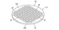
以下、本発明の実施形態を図面を参照して詳細に説明する。図1を参照すると、半導体ウェーハ(以下、単にウェーハと略称することがある)11の表面側斜視図が示されている。半導体ウェーハ11は、所定厚み(例えば700μm)のシリコン基板13上に複数の半導体デバイス19を形成する積層体15が積層されて構成されている。 Hereinafter, embodiments of the present invention will be described in detail with reference to the drawings. Referring to FIG. 1, a front side perspective view of a semiconductor wafer 11 (hereinafter sometimes simply referred to as a wafer) 11 is shown. The
各デバイス19は格子状に形成された複数の分割予定ライン17で区画された領域に形成されている。本実施形態の半導体ウェーハ11では、デバイス19形成時に層間絶縁膜として低誘電率絶縁膜(Low−k膜)が使用されている。 Each
本発明第1実施形態のウェーハの加工方法では、まず、図2に示すように、ウェーハ11の表面11aを外周部が環状フレームFに貼着されたダイシングテープTに貼着し、ウェーハ11の裏面11bを露出させる。 In the wafer processing method according to the first embodiment of the present invention, first, as shown in FIG. 2, the
本実施形態では、ダイシングテープTがウェーハ11の表面11aに形成されたデバイス19を保護する保護部材として作用する。従って、これを保護部材配設ステップと称することにする。 In the present embodiment, the dicing tape T functions as a protective member that protects the
保護部材配設ステップを実施後、図3に示したように、レーザー加工装置のチャックテーブル10でウェーハ11の裏面11b側を吸引保持し、環状フレームFの上に同一形状の第2の環状フレーム50を重ねてダイシングテープTの外周部をサンドイッチし、この状態でクランプ52により第2の環状フレーム50をクランプして固定する。 After carrying out the protective member arranging step, as shown in FIG. 3, the
保護テープ貼着ステップを実施した後、図3に示したように、ダイシングテープT及びウェーハ11に対して透過性を有し積層体15に対して吸収性を有する波長のレーザービームをダイシングテープT越しにウェーハ11に照射し、積層体15を部分的に除去してウェーハ11の表面に分割予定ライン17に沿ってレーザー加工溝23を形成するとともに、ウェーハ11の内部にウェーハ11の破断起点となる改質層25が同時に形成するレーザー加工ステップを実施する。 After performing the protective tape sticking step, as shown in FIG. Then, the
このレーザー加工ステップでは、レーザービームの集光点を積層体15近傍のウェーハ11の内部に位置付けてレーザービームを照射することが重要である。例えば、レーザービームの集光点をウェーハ11の表面11aから20〜30μm程度の深さに位置付けて、レーザービームをダイシングテープT越しにウェーハ11に照射する。 In this laser processing step, it is important to irradiate the laser beam with the condensing point of the laser beam positioned inside the
これにより、積層体15が部分的に除去されてウェーハ11の表面にレーザー加工溝23が形成されるとともに、ウェーハ11の表面11aから20〜30μm程度の深さに改質層25が同時に形成される。 As a result, the
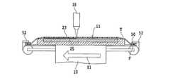
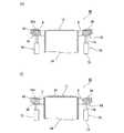
図3及び図4を参照すると、レーザービーム照射ユニット12は、ケーシング中に収容されたレーザービーム発生ユニット16と、ケーシングの先端に取り付けられた集光器(レーザーヘッド)18とから構成される。 3 and 4, the laser
レーザービーム発生ユニット16は、図4に示すように、YAGパルスレーザー又はYVO4パルスレーザーを発振するレーザー発振器22と、繰り返し周波数設定手段24と、パルス幅調整手段26と、パワー調整手段28とを含んでいる。特に図示しないが、レーザー発振器22はブリュースター窓を有しており、レーザー発振器22から出射するレーザービームは直線偏光のレーザービームである。 As shown in FIG. 4, the laser
レーザービーム発生ユニット16のパワー調整手段28で所定パワーに調整されたパルスレーザービームは、集光器18のミラー30で反射され、更に集光用対物レンズ32で集光されてチャックテーブル10に保持されたウェーハ11にダイシングテープT越しに照射される。 The pulse laser beam adjusted to a predetermined power by the power adjusting means 28 of the laser
レーザー加工ステップを実施する前に、分割予定ライン17を加工送り方向と平行で且つ集光器18と整列させるアライメントステップを実施する。アライメントステップは、図示しない撮像ユニットの赤外線撮像手段を用いてダイシングテープT越しに分割予定ライン17を検出して実施する。このアライメントステップは、第1の方向に伸長する分割予定ライン17と、第1の方向に直交する分割予定ライン17について実施する。 Before performing the laser processing step, an alignment step is performed in which the planned
アライメントステップ実施後、集光器18をレーザー加工すべき分割予定ライン17に整列させて、ダイシングテープT及びウェーハ11のシリコン基板13に対して透過性を有しウェーハ11の積層体15に対して吸収性を有する波長のレーザービームをダイシングテープT越しにウェーハ11に照射し、チャックテーブル10を矢印X1方向に加工送りすることにより、ウェーハ11の積層体10を部分的に除去して分割予定ライン17に沿ったレーザー加工溝23を形成するとともに、ウェーハ11の内部に改質層25を同時に形成するレーザー加工ステップを実施する。 After performing the alignment step, the
チャックテーブル10を加工送り方向X1と直交する方向に分割予定ライン17の間隔ずつ割り出し送りしながら、第1の方向に伸長する分割予定ライン17に沿って積層体15に同様なレーザー加工溝23を形成するとともに、ウェーハ11の内部に改質層25を次々と形成する。 While the chuck table 10 is indexed and fed in the direction orthogonal to the machining feed direction X1 at intervals of the planned division lines 17, the same
第1の方向に伸長する全ての分割予定ライン17に沿ってレーザー加工溝23及び改質層25の形成終了後、チャックテーブル10を90°回転して、第1の方向に直交する第2の方向に伸長する全ての分割予定ライン17に沿ってウェーハ11の積層体15にレーザー加工溝23を形成するとともにウェーハ11の内部に改質層25を同時に形成する。 After completing the formation of the
レーザー加工ステップにおけるレーザー加工条件は、例えば以下のとおりである。 The laser processing conditions in the laser processing step are, for example, as follows.
波長 :500nm〜1000nm
平均出力 :0.5W
繰り返し周波数 :100kHz
送り速度 :300mm/sWavelength: 500 nm to 1000 nm
Average output: 0.5W
Repetition frequency: 100 kHz
Feeding speed: 300mm / s
レーザー加工ステップを実施した後、ウェーハ11の裏面11bを研削してウェーハ11を仕上げ厚みへと薄化するとともに、研削押圧力によりウェーハ11を改質層25を分割起点に個々のデバイスチップへと分割する分割ステップを実施する。After performing the laser processing step, the
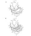
この分割ステップについて図5を参照して説明する。分割ステップでは、図5(A)に示すように、研削装置のチャックテーブル36によりウェーハ11の表面11a側をダイシングテープTを介して吸引保持し、ウェーハ11の裏面11b側を露出させる。 This division step will be described with reference to FIG. In the dividing step, as shown in FIG. 5A, the
研削装置の研削ユニット38は、モータにより回転駆動されるスピンドル40と、スピンドル40の先端に固定されたホイールマウント42と、ホイールマウント42に複数のねじ43で着脱可能に固定された研削ホイール44とを含んでいる。研削ホイール44は環状のホイール基台46と、ホイール基台46の下端外周部に環状に固着された複数の研削砥石48とから構成される。 The grinding
分割ステップでは、チャックテーブル36を矢印a方向に例えば300rpmで回転しつつ、研削ホイール44をチャックテーブル36と同一方向に、即ち矢印b方向に例えば6000rpmで回転させるとともに、図示しない研削ユニット送り機構を駆動して、研削砥石48をウェーハ11の裏面11bに接触させる。 In the dividing step, while rotating the chuck table 36 in the direction of arrow a at 300 rpm, for example, the grinding
そして、研削ホイール44を所定の研削送り速度で下方に所定量研削送りして、ウェーハ11を研削して所望の厚さに加工する。ウェーハ11の研削中にはウェーハ11の裏面11bに研削押圧力が掛かるため、ウェーハ11は強度が低下された改質層25を分割起点に、図5(B)に示すように、分割溝27で画成された個々のデバイスチップ29に分割される。 Then, the grinding
本実施形態のウェーハの加工方法では、レーザー加工ステップでウェーハ11の内部に改質層25が形成されるとともにウェーハ11の積層体15に分割予定ライン17に沿ったレーザー加工溝23が形成されるため、積層体15がLow−k膜等の分離しにくい材料を含んでいる場合にも、積層体15部分の分割位置がずれたり、積層体15がウェーハ11の基板13表面から分離したりするという問題が発生することはない。 In the wafer processing method of this embodiment, the modified
次に、本発明第2実施形態のウェーハの加工方法について、図6乃至図8を参照して説明する。本実施形態の加工方法では、まず、ウェーハ11の裏面11bを研削してウェーハ11を所定厚さに加工する研削ステップを実施する。この研削ステップでは、図6に示すように、研削装置のチャックテーブル36でダイシングテープTを介してウェーハ11を吸引保持し、ウェーハ11の裏面11bを露出させる。 Next, a wafer processing method according to the second embodiment of the present invention will be described with reference to FIGS. In the processing method of this embodiment, first, a grinding step is performed in which the
好ましくは、この時図示しない研削装置のクランプで環状フレームFをクランプして環状フレームFを下方に引き落とし、ウェーハ11の研削ステップで環状フレームFが邪魔にならないようにする。 Preferably, at this time, the annular frame F is clamped by a clamp of a grinding device (not shown) and the annular frame F is pulled downward so that the annular frame F does not get in the way in the grinding step of the
研削ステップでは、チャックテーブル36を矢印a方向に例えば300rpmで回転しつつ、研削ホイール44をチャックテーブル36と同一方向に、即ち矢印b方向に例えば6000rpmで回転させるとともに、図示しない研削ユニット送り機構を駆動して、研削砥石48をウェーハ11の裏面11bに接触させる。 In the grinding step, while rotating the chuck table 36 in the direction of arrow a at 300 rpm, for example, the grinding
そして、研削ホイール44を所定の研削送り速度で下方に所定量研削送りして、ウェーハ11の研削を実施する。接触式又は非接触式の厚み測定ゲージでウェーハ11の厚みを測定しながら、ウェーハ11を所望の厚み、例えば100μmに仕上げる。 Then, the grinding
研削ステップ実施後、ダイシングテープT及びウェーハ11の基板13に対して透過性を有し積層体15に対して吸収性を有する波長のレーザービームをダイシングテープT越しにウェーハ11の分割予定ライン17に沿って照射し、積層体15を部分的に除去してウェーハの表面にレーザー加工溝23を形成するとともに、ウェーハ11の内部にウェーハ11の破断起点となる改質層25を同時に形成するレーザー加工ステップを実施する。 After the grinding step is performed, a laser beam having a wavelength that is transmissive to the dicing tape T and the
このレーザー加工ステップは、図3及び図4を参照して説明した第1実施形態のレーザー加工ステップと同様であるので、ここではその詳細な説明を省略する。 Since this laser processing step is the same as the laser processing step of the first embodiment described with reference to FIGS. 3 and 4, detailed description thereof is omitted here.
レーザー加工ステップ実施後、レーザー加工溝23及び改質層25が形成されたウェーハ11に対して外力を付与し、分割予定ライン17に沿ってウェーハ11を個々のデバイスチップ29に分割する分割ステップを実施する。 After performing the laser processing step, a dividing step is performed in which an external force is applied to the
この分割ステップには、図8に示すような分割装置60を使用する。図8(A)において、分割装置60は環状フレームFを支持するフレーム保持ユニット62と、フレーム保持ユニット62に保持された環状フレームFに装着されたダイシングテープTを拡張する拡張ドラム64を具備している。 In this dividing step, a dividing
フレーム保持ユニット60は、環状のフレーム保持部材66と、フレーム保持部材66の外周に配設された固定手段としての複数のクランプ68から構成される。フレーム保持部材66の上面は環状フレームFを載置する載置面66aを形成しており、この載置面66a上に環状フレームFが載置される。 The
フレーム保持ユニット62は、エアシリンダ72から構成された駆動手段70により、環状のフレーム保持部材66をその載置面66aが拡張ドラム64の上端と略同一高さとなる基準位置と、拡張ドラム64の上端より所定量下方の拡張位置の間を上下方向に移動する。エアシリンダ72のピストンロッド74がフレーム保持部材66の下面に連結されている。 The
分割ステップでは、図8(A)に示すように、ウエーハ11をダイシングテープTを介して支持した環状フレームFを、フレーム保持部材66の載置面66a上に載置し、クランプ68によってフレーム保持部材66を固定する。このとき、フレーム保持部材66はその載置面66aが拡張ドラム64の上端と略同一高さとなる基準位置に位置付けられる。 In the dividing step, as shown in FIG. 8A, the annular frame F that supports the
次いで、エアシリンダ72を駆動してフレーム保持部材66を図8(B)に示す拡張位置に下降する。これにより、フレーム保持部材66の載置面66a上に固定されている環状フレームFも下降するため、環状フレームFに装着されたダイシングテープTは拡張ドラム64の上端縁に当接して主に半径方向に拡張される。 Next, the
その結果、ダイシングテープTに貼着されているウェーハ11には放射状に引っ張り力が作用する。このようにウェーハ11に放射状に引っ張り力が作用すると、ウェーハ11の内部に形成された改質層25は強度が低下されているので、改質層25が分割起点となってウェーハ11は分割予定ライン17に沿って個々のデバイスチップ29に分割される。 As a result, a tensile force acts radially on the
本実施形態でも、レーザー加工ステップでウェーハ11の積層体15には分割予定ライン17に沿ったレーザー加工溝23がウェーハ11内部に形成される改質層25と同時に形成されるため、積層体15がLow−k膜等の分離しにくい材料を含んでいる場合であっても、積層体15部分の分割位置がずれたり、積層体15がウェーハ11の基板13上面から剥離したりするという問題が発生することがない。 Also in the present embodiment, since the
上述した第1実施形態では、図3に示したレーザー加工ステップ及び図5に示した分割ステップを環状フレームFに貼着したダイシングテープTを張り替える必要がなく実施できる。 In the first embodiment described above, the laser processing step shown in FIG. 3 and the dividing step shown in FIG. 5 can be performed without the need to replace the dicing tape T attached to the annular frame F.
また、第2実施形態では、図6に示した研削ステップ、図7に示したレーザー加工ステップ及び図8に示した分割ステップを実施するのに、環状フレームFに貼着したダイシングテープTを張り替える必要がない。従って、加工方法は効率的であり、生産性が向上する。 Further, in the second embodiment, the dicing tape T attached to the annular frame F is replaced in order to perform the grinding step shown in FIG. 6, the laser processing step shown in FIG. 7, and the dividing step shown in FIG. There is no need to Therefore, the processing method is efficient and productivity is improved.
上述した第1及び第2実施形態では、レーザービームをダイシングテープT越しにウェーハ11に照射し、積層体15を部分的に除去して分割予定ライン17に沿ったレーザー加工溝23を形成するため、デバイス部分にデブリが飛散するのをウェーハの表面に配設されたダイシングテープTで防止することができる。レーザービームをダイシングテープT越しに照射するため、従来必要であった保護膜塗付工程が不要となる。 In the first and second embodiments described above, the laser beam is irradiated onto the
11 半導体ウェーハ
12 レーザービーム照射ユニット
13 シリコン基板
15 積層体
16 レーザービーム発生ユニット
17 分割予定ライン
18 集光器
19 デバイス
23 レーザー加工溝
25 改質層
27 分割溝
29 デバイスチップ
38 研削ユニット
42 フレーム保持ユニット
44 研削ホイール
60 分割装置
64 拡張ドラムDESCRIPTION OF
Claims (4)
Translated fromJapaneseウェーハに対して透過性を有し該積層体に対して吸収性を有する波長のレーザービームを該積層体側から該分割予定ラインに沿ってウェーハに照射し、該積層体を部分的に除去してウェーハの表面にレーザー加工溝を形成するとともに、ウェーハの内部にウェーハの破断起点となる改質層を同時に形成するレーザー加工ステップと、
該レーザー加工ステップを実施した後、ウェーハに外力を付与して該分割予定ラインに沿ってウェーハを個々のデバイスチップに分割する分割ステップと、を備え、
該レーザー加工ステップでは、レーザービームの集光点を該積層体近傍のウェーハ内部に位置付けることを特徴とするウェーハの加工方法。A wafer processing method for dividing a wafer on which a plurality of devices are formed by a laminate laminated on a surface of a substrate, along a division planned line that divides the plurality of devices,
A laser beam having a wavelength that is transparent to the wafer and absorbable to the laminated body is irradiated from the laminated body side along the planned dividing line to the wafer, and the laminated body is partially removed. A laser processing step for forming a laser processing groove on the surface of the wafer, and simultaneously forming a modified layer to be a fracture starting point of the wafer inside the wafer;
A step of dividing the wafer into individual device chips along the planned dividing line by applying an external force to the wafer after performing the laser processing step; and
In the laser processing step, a condensing point of a laser beam is positioned inside the wafer in the vicinity of the stacked body, and the wafer processing method is characterized in that:
該レーザー加工ステップでは、レーザービームの波長は該保護部材に対して透過性を有し、該保護部材越しにウェーハに該レーザービームを照射することを特徴とする請求項1〜3の何れかに記載のウェーハの加工方法。Before carrying out the laser processing step, further comprising a protective member disposing step of disposing a protective member on the surface of the wafer,
4. The laser processing step according to claim 1, wherein a wavelength of the laser beam is transmissive to the protective member, and the wafer is irradiated with the laser beam through the protective member. The processing method of the wafer as described.
Priority Applications (1)
| Application Number | Priority Date | Filing Date | Title |
|---|---|---|---|
| JP2014022661AJP6270520B2 (en) | 2014-02-07 | 2014-02-07 | Wafer processing method |
Applications Claiming Priority (1)
| Application Number | Priority Date | Filing Date | Title |
|---|---|---|---|
| JP2014022661AJP6270520B2 (en) | 2014-02-07 | 2014-02-07 | Wafer processing method |
Publications (2)
| Publication Number | Publication Date |
|---|---|
| JP2015149445Atrue JP2015149445A (en) | 2015-08-20 |
| JP6270520B2 JP6270520B2 (en) | 2018-01-31 |
Family
ID=53892573
Family Applications (1)
| Application Number | Title | Priority Date | Filing Date |
|---|---|---|---|
| JP2014022661AActiveJP6270520B2 (en) | 2014-02-07 | 2014-02-07 | Wafer processing method |
Country Status (1)
| Country | Link |
|---|---|
| JP (1) | JP6270520B2 (en) |
Cited By (2)
| Publication number | Priority date | Publication date | Assignee | Title |
|---|---|---|---|---|
| JP2017118096A (en)* | 2015-09-10 | 2017-06-29 | 株式会社ディスコ | Substrate processing method |
| CN110788499A (en)* | 2018-08-02 | 2020-02-14 | 株式会社迪思科 | wafer processing method |
Citations (8)
| Publication number | Priority date | Publication date | Assignee | Title |
|---|---|---|---|---|
| JP2006150385A (en)* | 2004-11-26 | 2006-06-15 | Canon Inc | Laser cleaving method |
| JP2006305586A (en)* | 2005-04-27 | 2006-11-09 | Cyber Laser Kk | Method for cutting plate-shaped body, and laser beam machining device |
| JP2007173475A (en)* | 2005-12-21 | 2007-07-05 | Disco Abrasive Syst Ltd | Wafer division method |
| US20080070378A1 (en)* | 2006-09-19 | 2008-03-20 | Jong-Souk Yeo | Dual laser separation of bonded wafers |
| JP2013031879A (en)* | 2012-09-04 | 2013-02-14 | Imra America Inc | Processing of transparent material by ultra-short pulse laser |
| JP2013058536A (en)* | 2011-09-07 | 2013-03-28 | Disco Abrasive Syst Ltd | Method for dividing device wafer |
| JP2013219076A (en)* | 2012-04-04 | 2013-10-24 | Disco Abrasive Syst Ltd | Method for processing optical device wafer |
| JP2013254867A (en)* | 2012-06-07 | 2013-12-19 | Disco Abrasive Syst Ltd | Wafer processing method |
- 2014
- 2014-02-07JPJP2014022661Apatent/JP6270520B2/enactiveActive
Patent Citations (8)
| Publication number | Priority date | Publication date | Assignee | Title |
|---|---|---|---|---|
| JP2006150385A (en)* | 2004-11-26 | 2006-06-15 | Canon Inc | Laser cleaving method |
| JP2006305586A (en)* | 2005-04-27 | 2006-11-09 | Cyber Laser Kk | Method for cutting plate-shaped body, and laser beam machining device |
| JP2007173475A (en)* | 2005-12-21 | 2007-07-05 | Disco Abrasive Syst Ltd | Wafer division method |
| US20080070378A1 (en)* | 2006-09-19 | 2008-03-20 | Jong-Souk Yeo | Dual laser separation of bonded wafers |
| JP2013058536A (en)* | 2011-09-07 | 2013-03-28 | Disco Abrasive Syst Ltd | Method for dividing device wafer |
| JP2013219076A (en)* | 2012-04-04 | 2013-10-24 | Disco Abrasive Syst Ltd | Method for processing optical device wafer |
| JP2013254867A (en)* | 2012-06-07 | 2013-12-19 | Disco Abrasive Syst Ltd | Wafer processing method |
| JP2013031879A (en)* | 2012-09-04 | 2013-02-14 | Imra America Inc | Processing of transparent material by ultra-short pulse laser |
Cited By (2)
| Publication number | Priority date | Publication date | Assignee | Title |
|---|---|---|---|---|
| JP2017118096A (en)* | 2015-09-10 | 2017-06-29 | 株式会社ディスコ | Substrate processing method |
| CN110788499A (en)* | 2018-08-02 | 2020-02-14 | 株式会社迪思科 | wafer processing method |
Also Published As
| Publication number | Publication date |
|---|---|
| JP6270520B2 (en) | 2018-01-31 |
Similar Documents
| Publication | Publication Date | Title |
|---|---|---|
| JP6078376B2 (en) | Wafer processing method | |
| CN105047612B (en) | wafer processing method | |
| JP4694845B2 (en) | Wafer division method | |
| JP5645593B2 (en) | Wafer division method | |
| JP6189208B2 (en) | Wafer processing method | |
| KR102349663B1 (en) | Wafer processing method | |
| JP5992731B2 (en) | Wafer processing method | |
| JP2009021476A (en) | Wafer division method | |
| JP2017041482A (en) | Wafer processing method | |
| JP2007173475A (en) | Wafer division method | |
| JP2016018881A (en) | Wafer processing method | |
| JP6246534B2 (en) | Wafer processing method | |
| KR20180050225A (en) | Method for processing wafer | |
| JP2014143285A (en) | Wafer processing method | |
| JP2015153770A (en) | Wafer processing method and processing apparatus | |
| JP6257365B2 (en) | Wafer processing method | |
| CN108015650A (en) | The processing method of chip | |
| JP5995428B2 (en) | Manufacturing method of chip with cover | |
| JP6558973B2 (en) | Device chip manufacturing method | |
| US9455149B2 (en) | Plate-like object processing method | |
| JP6270520B2 (en) | Wafer processing method | |
| JP2018067646A (en) | Wafer processing method | |
| JP2011114018A (en) | Method of manufacturing optical device | |
| JP5863264B2 (en) | Wafer processing method | |
| JP2016076522A (en) | Wafer processing method |
Legal Events
| Date | Code | Title | Description |
|---|---|---|---|
| A621 | Written request for application examination | Free format text:JAPANESE INTERMEDIATE CODE: A621 Effective date:20161213 | |
| A131 | Notification of reasons for refusal | Free format text:JAPANESE INTERMEDIATE CODE: A131 Effective date:20170815 | |
| A977 | Report on retrieval | Free format text:JAPANESE INTERMEDIATE CODE: A971007 Effective date:20170817 | |
| A521 | Request for written amendment filed | Free format text:JAPANESE INTERMEDIATE CODE: A523 Effective date:20171012 | |
| TRDD | Decision of grant or rejection written | ||
| A01 | Written decision to grant a patent or to grant a registration (utility model) | Free format text:JAPANESE INTERMEDIATE CODE: A01 Effective date:20171226 | |
| A61 | First payment of annual fees (during grant procedure) | Free format text:JAPANESE INTERMEDIATE CODE: A61 Effective date:20171226 | |
| R150 | Certificate of patent or registration of utility model | Ref document number:6270520 Country of ref document:JP Free format text:JAPANESE INTERMEDIATE CODE: R150 | |
| R250 | Receipt of annual fees | Free format text:JAPANESE INTERMEDIATE CODE: R250 | |
| R250 | Receipt of annual fees | Free format text:JAPANESE INTERMEDIATE CODE: R250 | |
| R250 | Receipt of annual fees | Free format text:JAPANESE INTERMEDIATE CODE: R250 | |
| R250 | Receipt of annual fees | Free format text:JAPANESE INTERMEDIATE CODE: R250 | |
| R250 | Receipt of annual fees | Free format text:JAPANESE INTERMEDIATE CODE: R250 |