JP2015121912A - Touch panel device and touch detection method - Google Patents
Touch panel device and touch detection methodDownload PDFInfo
- Publication number
- JP2015121912A JP2015121912AJP2013264855AJP2013264855AJP2015121912AJP 2015121912 AJP2015121912 AJP 2015121912AJP 2013264855 AJP2013264855 AJP 2013264855AJP 2013264855 AJP2013264855 AJP 2013264855AJP 2015121912 AJP2015121912 AJP 2015121912A
- Authority
- JP
- Japan
- Prior art keywords
- touch
- difference data
- touch panel
- data
- frame
- Prior art date
- Legal status (The legal status is an assumption and is not a legal conclusion. Google has not performed a legal analysis and makes no representation as to the accuracy of the status listed.)
- Granted
Links
Images


Landscapes
- Position Input By Displaying (AREA)
Abstract
Description
Translated fromJapaneseこの発明は、静電容量方式のタッチパネル装置およびタッチパネルのタッチ検出方法に関する。 The present invention relates to a capacitive touch panel device and a touch detection method for a touch panel.
静電容量方式のタッチパネル装置は、指の接触等による静電容量の変化を測定することによってタッチポイントを検出するものであり、例えば携帯電話やタブレットPC等に適用されている(例えば、特許文献1参照)。 A capacitive touch panel device detects a touch point by measuring a change in capacitance due to a finger touch or the like, and is applied to, for example, a mobile phone or a tablet PC (for example, Patent Documents). 1).
図4は、従来の静電容量方式のタッチパネル装置を備えた表示装置の駆動回路を示すブロック図である。図4において、この駆動回路は、タッチパネル10およびタッチパネル10に接続されたタッチパネルコントローラ20と、LCD(Liquid Crystal Display)30およびLCD30に接続されたタイミングコントローラ40と、タッチパネルコントローラ20およびタイミングコントローラ40に接続されたホストコントローラ50とを備えている。 FIG. 4 is a block diagram illustrating a driving circuit of a display device including a conventional capacitive touch panel device. 4, this drive circuit is connected to the
タッチパネルコントローラ20は、タッチパネル10の駆動電極Txに駆動信号(センシング信号)を出力するとともに、タッチパネル10の読み出し電極Rxからスキャン信号が入力される。また、タッチパネルコントローラ20は、入力されたスキャン信号に基づいて、タッチの有無を含む座標データ信号をホストコントローラ50に出力する。 The
タイミングコントローラ40は、ホストコントローラ50から入力されるクロック信号、画像データ信号および水平同期信号に基づいて、LCD10にLCD制御信号を出力し、LCD30の液晶書き込みを実行する。なお、画像データ信号には、タッチパネルコントローラ20からの座標データに基づいて、ホストコントローラ50で内部処理された画像データが含まれる。 The
図5は、図4に示したタッチパネル10を構成する電極を示す説明図である。図5において、タッチパネル10は、複数本の駆動電極Tx(例えば、Tx1〜Tx6センサライン)と、駆動電極Txと絶縁された複数本の読み出し電極Rx(例えば、Rx1〜Rx6センサライン)とを有している。また、タッチパネル10は、LCD30の上部に取り付けられるので、ITO(Indium Tin Oxide)等の透明かつ導電性がある材料が用いられる。 FIG. 5 is an explanatory diagram showing electrodes constituting the
図6は、図4に示したタッチパネル10において、タッチの有無による駆動電極Txと読み出し電極Rxとの相互容量の変化を示す説明図である。図6において、(a)はタッチがない場合の相互容量を示し、(b)はタッチがある場合の相互容量を示し、図中の電極間の点線は、電気力線を示している。 FIG. 6 is an explanatory diagram showing a change in mutual capacitance between the drive electrode Tx and the read electrode Rx depending on the presence or absence of touch in the
また、図6(a)において、タッチがない場合の駆動電極Txと読み出し電極Rxとの間の相互容量をCm1+Cm2とする。図6(b)において、タッチがある場合には、指が導電性を有しているので、指が電極となってCm2がなくなり、代わりにCt−f(駆動電極Txと指との間の静電容量)およびCr−f(指と読み出し電極Rxとの間の静電容量)が発生する。 In FIG. 6A, the mutual capacitance between the drive electrode Tx and the read electrode Rx when there is no touch is Cm1 + Cm2. In FIG. 6B, when there is a touch, since the finger has conductivity, the finger becomes an electrode and Cm2 disappears. Instead, Ct−f (between the drive electrode Tx and the finger). Capacitance) and Cr-f (capacitance between the finger and the readout electrode Rx) are generated.
図7は、図6に示したタッチパネル10の静電容量の等価回路を示す回路図である。図7において、(a)はタッチがない場合の等価回路を示し、(b)はタッチがある場合の等価回路を示している。図7において、駆動電極Txのセンサラインに付く付加容量をCtxとし、読み出し電極Rxのセンサラインに付く付加容量をCrxとする。 FIG. 7 is a circuit diagram showing an equivalent circuit of the capacitance of the
また、図7(a)において、タッチがない場合の駆動電極Txと読み出し電極Rxとの間の相互容量は、図6(a)に示したように、Cm1+Cm2である。また、図7(b)において、タッチされることによって、図6(b)に示したように、Cm2がなくなり、指との間に発生するCt−fおよびCr−fが付加される。 In FIG. 7A, the mutual capacitance between the drive electrode Tx and the read electrode Rx when there is no touch is Cm1 + Cm2, as shown in FIG. 7B, when touched, Cm2 disappears and Ct-f and Cr-f generated between the fingers are added as shown in FIG. 6B.
図8は、図7に示した等価回路から、過渡応答を考慮しない電圧に関係する部分のみを抽出した等価回路を示す回路図である。図8において、(a)はタッチがない場合の等価回路を示し、(b)はタッチがある場合の等価回路を示している。 FIG. 8 is a circuit diagram showing an equivalent circuit obtained by extracting only the portion related to the voltage not considering the transient response from the equivalent circuit shown in FIG. 8A shows an equivalent circuit when there is no touch, and FIG. 8B shows an equivalent circuit when there is a touch.
また、図8(a)において、タッチがない場合に、読み出し電極Rxに現れる電圧Vrxは、次式(1)で表される。 In FIG. 8A, the voltage Vrx that appears at the readout electrode Rx when there is no touch is expressed by the following equation (1).
(Cm1+Cm2)×(Vtx−Vrx)=Crx×Vrx
Vrx=(Cm1+Cm2)/(Cm1+Cm2+Crx)×Vtx・・・(1)(Cm1 + Cm2) × (Vtx−Vrx) = Crx × Vrx
Vrx = (Cm1 + Cm2) / (Cm1 + Cm2 + Crx) × Vtx (1)
続いて、図8(b)において、タッチがある場合に、読み出し電極Rxに現れる電圧Vrx’は、次式(2)で表される。 Subsequently, in FIG. 8B, when there is a touch, the voltage Vrx ′ appearing on the readout electrode Rx is expressed by the following equation (2).
Cm1(Vtx−Vrx)=(Crx+Cr−f)×Vrx’
Vrx’=Cm1/(Cm1+Crx+Cr−f)×Vtx・・・(2)Cm1 (Vtx−Vrx) = (Crx + Cr−f) × Vrx ′
Vrx ′ = Cm1 / (Cm1 + Crx + Cr−f) × Vtx (2)
また、読み出し電極Rxに現れる電圧Vrxと電圧Vrx’との関係は、次式(3)で表される。 Further, the relationship between the voltage Vrx and the voltage Vrx ′ appearing at the readout electrode Rx is expressed by the following equation (3).
Vrx:Vrx’
=(Cm1+Cm2)/(Cm1+Cm2+Crx):Cm1/(Cm1+Crx+Cr−f)
=(Cm1+Cm2)×(Cm1+Crx+Cr−f):Cm1×(Cm1+Cm2+Crx)
=Cm12+Cm1×Cm2+Cm1×Crx+Cm1×Cr−f+Cm2×Crx+Cm2×Cr−f:Cm12+Cm1×Cm2+Cm1×Crx・・・(3)Vrx: Vrx '
= (Cm1 + Cm2) / (Cm1 + Cm2 + Crx): Cm1 / (Cm1 + Crx + Cr−f)
= (Cm1 + Cm2) × (Cm1 + Crx + Cr−f): Cm1 × (Cm1 + Cm2 + Crx)
= Cm12 + Cm1 * Cm2 + Cm1 * Crx + Cm1 * Cr-f + Cm2 * Crx + Cm2 * Cr-f: Cm12 + Cm1 * Cm2 + Cm1 * Crx (3)
ここで、Cm12+Cm1×Cm2+Cm1×Crx=Csumとすると、上記式(3)は、次式(4)で表される。Here, when Cm12 + Cm1 × Cm2 + Cm1 × Crx = Csum, the above equation (3) is expressed by the following equation (4).
Vrx:Vrx’=Csum+Cm1×Cr−f+Cm2×Crx+Cm2×Cr−f:Csum・・・(4) Vrx: Vrx ′ = Csum + Cm1 × Cr−f + Cm2 × Crx + Cm2 × Cr−f: Csum (4)
式(4)から、読み出し電極Rxに現れる電圧Vrxと電圧Vrx’とは、Vrx>Vrx’の関係にあることがわかる。 From Expression (4), it can be seen that the voltage Vrx and the voltage Vrx ′ appearing at the readout electrode Rx are in a relationship of Vrx> Vrx ′.
図9は、図7に示した等価回路の駆動電極Txに、パルス電圧Vtxの駆動信号を印加した場合の、読み出し電極Rxに現れる電圧を示す説明図である。図9において、(a)は駆動電極Txの電圧を示し、(b)はタッチがない場合の読み出し電極Rxの電圧を示し、(c)はタッチがある場合の読み出し電極Rxの電圧を示している。 FIG. 9 is an explanatory diagram showing a voltage appearing on the read electrode Rx when a drive signal of the pulse voltage Vtx is applied to the drive electrode Tx of the equivalent circuit shown in FIG. In FIG. 9, (a) shows the voltage of the drive electrode Tx, (b) shows the voltage of the read electrode Rx when there is no touch, and (c) shows the voltage of the read electrode Rx when there is a touch. Yes.
図9より、図8で説明したように、タッチがある場合の電圧Vrx’は、タッチがない場合の電圧Vrxよりも小さくなることがわかる。また、図9において、電圧Vrxと電圧Vrx’との差ΔVrxは、実際には小さい値なので、1フレームで駆動電極Txに複数のパルス電圧Vtxを印加し、電圧差ΔVrxを複数回積分することで、タッチの有無を検出している。 As can be seen from FIG. 9, the voltage Vrx ′ when there is a touch is smaller than the voltage Vrx when there is no touch, as described with reference to FIG. 8. In FIG. 9, since the difference ΔVrx between the voltage Vrx and the voltage Vrx ′ is actually a small value, a plurality of pulse voltages Vtx are applied to the drive electrode Tx in one frame, and the voltage difference ΔVrx is integrated a plurality of times. The presence of touch is detected.
図10は、図4に示したタッチパネルコントローラ20の構成を詳細に示すブロック図である。図10において、タッチパネルコントローラ20は、Txパルス発生部21、Rx検出部22、座標計算部23およびタッチなしメモリ24を有している。また、Rx検出部22は、積分回路22aおよびA/D変換部22bを含んでいる。 FIG. 10 is a block diagram showing in detail the configuration of the
Txパルス発生部21は、複数のパルス電圧Vtxを、図5に示した駆動電極Txの各センサラインに印加する。Rx検出部22は、各Txセンサライン単位で印加された複数のパルス電圧Vtxを、図7に示した等価回路を通してスキャン信号として検出し、検出されたデータを積分回路22aで積分した後に、積分結果をA/D変換部22bでA/D変換して出力する。 The
図11は、図10に示した座標計算部23によるタッチポイントの検出を具体的に説明するための図である。図11を参照して、座標計算部23は、Rx検出部22で得られた検出データと、タッチなしメモリ24に記憶されたタッチなし記憶データ(所定のベースデータ)との差分をとって、差分データを生成する。 FIG. 11 is a diagram for specifically explaining detection of a touch point by the
また、座標計算部23は、生成された差分データがあらかじめ定められた一定の閾値以上である場合には、タッチがあるものとみなしてタッチポイントの座標を計算し、座標データ信号を出力する。なお、タッチなし記憶データは、タッチがない状態のデータとして、あらかじめタッチなしメモリ24に記憶されたデータである。 Further, when the generated difference data is equal to or greater than a predetermined threshold value, the
以下、図12のフローチャートを参照しながら、図10に示したタッチパネルコントローラ20の処理について説明する。なお、図12のフローチャートは、1フレーム分の処理を示している。 Hereinafter, the processing of the
まず、Txパルス発生部21およびRx検出部22は、駆動電極Txの各センサラインをスキャン(各センサラインにパルス電圧Vtxを印加)するとともに、読み出し電極Rxから検出データを取得する(ステップS1)。 First, the
続いて、座標計算部23は、Rx検出部22からの検出データとタッチなしメモリ24に記憶されたタッチなし記憶データとの差分をとって、差分データを生成する(ステップS2)。 Subsequently, the coordinate
次に、座標計算部23は、生成された差分データに基づいて、タッチの有無を判定する(ステップS3)。 Next, the coordinate
ステップS3において、タッチがある(すなわち、Yes)と判定された場合には、座標計算部23は、タッチポイントの座標を計算し、座標データ信号を出力して(ステップS4)、ステップS1に移行する。 If it is determined in step S3 that there is a touch (that is, Yes), the coordinate
一方、ステップS3において、タッチがない(すなわち、No)と判定された場合には、座標計算部23は、タッチポイントの座標を計算することなく、ステップS1に移行する。 On the other hand, if it is determined in step S3 that there is no touch (that is, No), the coordinate
ここで、あるフレームで、ステップS1において駆動電極Txの各センサラインがスキャンされ、次のフレームで、再びステップS1において駆動電極Txの各センサラインがスキャンされるまでの間隔(周期)は、60〜120Hzであり、この間隔毎に、タッチの有無が検出され、タッチポイントの座標が計算される。 Here, in a certain frame, each sensor line of the drive electrode Tx is scanned in step S1, and in the next frame, the interval (cycle) until each sensor line of the drive electrode Tx is scanned again in step S1 is 60. The presence / absence of a touch is detected at each interval, and the coordinates of the touch point are calculated.
しかしながら、従来技術には、以下のような課題がある。
静電容量方式のタッチパネル装置では、圧力による接触を感知する抵抗膜方式とは異なり、非導電性の手袋等(以下、単に「手袋」とも称する)を着用した状態で、タッチポイントを検出することが困難になる。However, the prior art has the following problems.
Capacitive touch panel devices detect touch points while wearing non-conductive gloves (hereinafter also simply referred to as “gloves”), unlike resistive film systems that sense pressure contact. Becomes difficult.
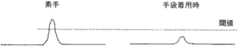
図13は、従来の静電容量方式のタッチパネル装置におけるタッチ信号を、素手の状態と手袋を着用した状態とで比較して示す説明図である。なお、タッチ信号は、座標計算部23によって生成された差分データである。図13において、手袋着用時のタッチ信号は、信号レベルが低く、ノイズ等の影響を考慮して設定された閾値に達しないので、タッチポイントを検出することができない。 FIG. 13 is an explanatory view showing a touch signal in a conventional capacitive touch panel device in comparison with a bare hand state and a gloved state. The touch signal is difference data generated by the coordinate
ここで、手袋着用時にタッチ信号の信号レベルが低くなるのは、手袋を着用することによって、タッチがない場合に読み出し電極Rxに現れる電圧Vrxと、タッチがある場合に読み出し電極Rxに現れる電圧Vrx’との差が小さくなることによる(上述した図8参照)。 Here, when the glove is worn, the signal level of the touch signal is lowered by wearing the glove so that the voltage Vrx that appears on the read electrode Rx when there is no touch and the voltage Vrx that appears on the read electrode Rx when there is a touch. This is because the difference from 'becomes smaller (see FIG. 8 described above).
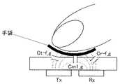
図14は、従来の静電容量方式のタッチパネル装置において、手袋を着用した状態でタッチした場合の駆動電極Txと読み出し電極Rxとの相互容量の変化を示す説明図である。図14において、非導電性の手袋を介することにより、指と読み出し電極Rxとの間の距離が広がるので、静電容量Cr−fが小さくなる(Cr−f_g)。 FIG. 14 is an explanatory diagram showing a change in mutual capacitance between the drive electrode Tx and the read electrode Rx when touched in a state where a glove is worn in a conventional capacitive touch panel device. In FIG. 14, the distance between the finger and the readout electrode Rx is increased by using a non-conductive glove, so that the capacitance Cr-f is reduced (Cr-f_g).
すなわち、上記式(4)(Vrx:Vrx’=Csum+Cm1×Cr−f+Cm2×Crx+Cm2×Cr−f:Csum)において、電圧Vrxと電圧Vrx’との差異の要因である静電容量Cr−fが小さくなるので、タッチ信号が小さくなる。 That is, in the above formula (4) (Vrx: Vrx ′ = Csum + Cm1 × Cr−f + Cm2 × Crx + Cm2 × Cr−f: Csum), the capacitance Cr−f that is a factor of the difference between the voltage Vrx and the voltage Vrx ′ is small. Therefore, the touch signal becomes small.
なお、タッチ信号の信号レベルを高くする方法として、電圧Vrx’の絶対値を大きくするために、パルス電圧Vtxを高くすることが考えられる。しかしながら、これは、消費電力が大きくなることから、実現困難である。 As a method for increasing the signal level of the touch signal, it is conceivable to increase the pulse voltage Vtx in order to increase the absolute value of the voltage Vrx ′. However, this is difficult to realize due to the increased power consumption.
また、別の方法として、駆動電極Txの各センサラインに印加する1フレーム中のパルス数を増やして、積分数を多くすることが考えられる。しかしながら、この場合には、図12に示したフローチャートの周期60〜120Hzを達成することが困難である。 As another method, it is conceivable to increase the number of integrations by increasing the number of pulses in one frame applied to each sensor line of the drive electrode Tx. However, in this case, it is difficult to achieve the period of 60 to 120 Hz in the flowchart shown in FIG.
そのため、冬場等気温が低い季節では、手袋を外してから操作を行う必要があったり、導電性の繊維を織り込んだ特別な手袋を購入する必要があったりして、利用者の利便性が低いという問題がある。 For this reason, it is necessary to remove the gloves before operation in winter when the temperature is low, such as in winter, or it is necessary to purchase special gloves woven with conductive fibers, resulting in low user convenience. There is a problem.
この発明は、上記のような課題を解決するためになされたものであり、非導電性の手袋を着用した状態であっても、タッチポイントを検出することができ、利用者の利便性を向上させることができるタッチパネル装置およびタッチ検出方法を得ることを目的とする。 The present invention has been made to solve the above-described problems, and can detect a touch point even when a non-conductive glove is worn, improving user convenience. It is an object to obtain a touch panel device and a touch detection method that can be performed.
この発明に係るタッチパネル装置は、静電容量方式のタッチパネルを備えたタッチパネル装置であって、タッチパネルの各センサで検出されたデータと、所定のベースデータとの差分をとって、1フレーム分の差分データを生成するとともに、差分データに基づいて、タッチの有無を検出する座標計算部と、差分データが記憶される積算メモリと、を備え、座標計算部は、1フレーム分の差分データに基づいてタッチが検出された場合に、タッチポイントの座標を計算し、1フレーム分の差分データに基づいてタッチが検出されない場合に、積算メモリにこの差分データを記憶するとともに、積算メモリに少なくとも2回以上積算した差分データに基づいて、タッチの有無を検出するものである。 The touch panel device according to the present invention is a touch panel device provided with a capacitive touch panel, and takes a difference between data detected by each sensor of the touch panel and predetermined base data to obtain a difference for one frame. A coordinate calculation unit that generates data and detects the presence / absence of a touch based on the difference data, and an integration memory that stores the difference data, the coordinate calculation unit based on the difference data for one frame When a touch is detected, the coordinates of the touch point are calculated, and when no touch is detected based on the difference data for one frame, the difference data is stored in the integration memory and at least twice or more in the integration memory. The presence or absence of a touch is detected based on the accumulated difference data.
この発明に係るタッチ検出方法は、静電容量方式のタッチパネルを備えたタッチパネル装置で実行されるタッチ検出方法であって、タッチパネルの各センサで検出されたデータと、所定のベースデータとの差分をとって、1フレーム分の差分データを生成する差分データ生成ステップと、1フレーム分の差分データに基づいてタッチが検出された場合に、タッチポイントの座標を計算する座標計算ステップと、1フレーム分の差分データに基づいてタッチが検出されない場合に、この差分データを記憶する記憶ステップと、少なくとも2回以上積算した差分データに基づいて、タッチの有無を検出する検出ステップと、を有するものである。 The touch detection method according to the present invention is a touch detection method executed by a touch panel device including a capacitive touch panel, and calculates a difference between data detected by each sensor of the touch panel and predetermined base data. A difference data generation step for generating difference data for one frame, a coordinate calculation step for calculating coordinates of a touch point when a touch is detected based on the difference data for one frame, and for one frame When a touch is not detected based on the difference data, a storage step for storing the difference data and a detection step for detecting presence or absence of the touch based on the difference data accumulated at least twice are provided. .
この発明に係るタッチパネル装置およびタッチ検出方法によれば、1フレーム分の差分データに基づいてタッチが検出された場合に、タッチポイントの座標を計算し、1フレーム分の差分データに基づいてタッチが検出されない場合に、この差分データを記憶するとともに、少なくとも2回以上積算した差分データに基づいて、タッチの有無を検出する。
そのため、非導電性の手袋を着用した状態であっても、タッチポイントを検出することができ、利用者の利便性を向上させることができる。According to the touch panel device and the touch detection method according to the present invention, when a touch is detected based on the difference data for one frame, the coordinates of the touch point are calculated, and the touch is detected based on the difference data for one frame. If not detected, the difference data is stored, and the presence or absence of a touch is detected based on the difference data accumulated at least twice.
Therefore, even in a state where non-conductive gloves are worn, the touch point can be detected, and the convenience for the user can be improved.
以下、この発明に係るタッチパネル装置およびタッチ検出方法の好適な実施の形態につき図面を用いて説明するが、各図において同一、または相当する部分については、同一符号を付して説明する。 Hereinafter, preferred embodiments of a touch panel device and a touch detection method according to the present invention will be described with reference to the drawings. In the drawings, the same or corresponding parts will be described with the same reference numerals.
実施の形態1.
まず、図1を参照しながら、この発明の要旨について説明する。図1は、この発明に係るタッチパネル装置およびタッチ検出方法の要旨を説明するための図である。図1において、上述したように、非導電性の手袋を着用した状態では、1フレームあたりのタッチ信号の信号レベルが低くなる。
First, the gist of the present invention will be described with reference to FIG. FIG. 1 is a diagram for explaining the gist of a touch panel device and a touch detection method according to the present invention. In FIG. 1, as described above, the signal level of the touch signal per frame is low when a non-conductive glove is worn.
しかしながら、図1に示したように、手袋を着用した状態であっても、複数フレーム分のタッチ信号を積算することにより、タッチ信号の合計値が閾値を超えることができる。したがって、非導電性の手袋を着用した状態であっても、タッチポイントを検出することができる。 However, as shown in FIG. 1, even when a glove is worn, the total value of the touch signals can exceed the threshold by integrating the touch signals for a plurality of frames. Therefore, a touch point can be detected even when a non-conductive glove is worn.
図2は、この発明の実施の形態1に係るタッチパネル装置のタッチパネルコントローラ20Aの構成を詳細に示すブロック図である。図2において、このタッチパネルコントローラ20Aは、図10に示した座標計算部23に代えて、座標計算部23Aを有し、積算メモリ25をさらに有している。タッチパネルコントローラ20Aのその他の構成は、図10に示したものと同様なので、説明を省略する。 FIG. 2 is a block diagram showing in detail the configuration of
座標計算部23Aは、Rx検出部22で得られた検出データと、タッチなしメモリ24に記憶されたタッチなし記憶データとの差分をとって、1フレーム分の差分データ(1フレーム分のタッチ信号)を生成する。また、座標計算部23Aは、1フレーム分のタッチ信号が閾値以上である場合には、タッチポイントの座標を計算し、座標データ信号を出力する。 The coordinate
一方、座標計算部23Aは、1フレーム分のタッチ信号でタッチポイントを検出できなかった場合には、タッチ信号を積算メモリ25に記憶するとともに、積算メモリ25にn(nは、任意に設定される2以上の整数)回積算したタッチ信号に基づいて、タッチの有無を検出する。なお、座標計算部23Aは、n回積算したタッチ信号によってもタッチポイントを検出できない場合には、積算メモリ25をリセットする。 On the other hand, when the coordinate
以下、図3のフローチャートを参照しながら、図2に示したタッチパネルコントローラ20Aの処理について説明する。なお、図3のフローチャートは、1フレーム分の処理を示している。 Hereinafter, the processing of the
まず、Txパルス発生部21およびRx検出部22は、駆動電極Txの各センサラインをスキャン(各センサラインにパルス電圧Vtxを印加)するとともに、読み出し電極Rxから検出データを取得する(ステップS1)。 First, the
続いて、座標計算部23は、Rx検出部22からの検出データとタッチなしメモリ24に記憶されたタッチなし記憶データとの差分をとって、差分データを生成する(ステップS2)。 Subsequently, the coordinate
次に、座標計算部23Aは、生成された差分データに基づいて、タッチの有無を判定する(ステップS3)。 Next, the coordinate
ステップS3において、タッチがある(すなわち、Yes)と判定された場合には、座標計算部23Aは、タッチポイントの座標を計算し、座標データ信号を出力する(ステップS4)。 If it is determined in step S3 that there is a touch (that is, Yes), the coordinate
続いて、座標計算部23Aは、積算メモリ25をリセットして(ステップS5)、ステップS1に移行する。 Subsequently, the coordinate
一方、ステップS3において、タッチがない(すなわち、No)と判定された場合には、座標計算部23Aは、タッチ信号(差分データ)を積算メモリ25に記憶する(ステップS6)。 On the other hand, if it is determined in step S3 that there is no touch (that is, No), the coordinate
次に、座標計算部23Aは、タッチ信号をn回積算したか否かを判定する(ステップS7)。 Next, the coordinate
ステップS7において、n回積算した(すなわち、Yes)と判定された場合には、座標計算部23Aは、n回積算したタッチ信号に基づいて、タッチの有無を判定する(ステップS8)。 If it is determined in step S7 that n times have been integrated (that is, Yes), the coordinate
ステップS8において、タッチがある(すなわち、Yes)と判定された場合には、ステップS4に移行して、座標計算部23Aは、タッチポイントの座標を計算し、座標データ信号を出力する。 If it is determined in step S8 that there is a touch (that is, Yes), the process proceeds to step S4, where the coordinate
一方、ステップS8において、タッチがない(すなわち、No)と判定された場合には、座標計算部23Aは、積算メモリ25をリセットして(ステップS9)、ステップS1に移行する。 On the other hand, if it is determined in step S8 that there is no touch (that is, No), the coordinate
また、ステップS7において、n回積算していない(すなわち、No)と判定された場合には、座標計算部23Aは、タッチポイントの座標を計算することなく、ステップS1に移行する。 If it is determined in step S7 that the integration has not been performed n times (that is, No), the coordinate
このように、複数フレーム分のタッチ信号を積算することにより、パルス電圧Vtxを高くすることなく、また、通常のタッチポイントの検出では、図3に示したフローチャートの周期60〜120Hzを維持したままで、現在は検出することができない非導電性の手袋を着用した状態のタッチポイントを検出することができる。 In this way, by integrating the touch signals for a plurality of frames, the pulse voltage Vtx is not increased, and the normal touch point detection is maintained with the period of 60 to 120 Hz in the flowchart shown in FIG. Thus, it is possible to detect a touch point in a state where a non-conductive glove that cannot be detected at present is worn.
以上のように、実施の形態1によれば、1フレーム分の差分データに基づいてタッチが検出された場合に、タッチポイントの座標を計算し、1フレーム分の差分データに基づいてタッチが検出されない場合に、この差分データを記憶するとともに、少なくとも2回以上積算した差分データに基づいて、タッチの有無を検出する。
そのため、利用者がタッチパネルを操作するために、着用していた手袋を外すという煩雑な作業から解放されるとともに、導電性の手袋を購入しなければならないという選択の自由の制限から解放される。
したがって、非導電性の手袋を着用した状態であっても、タッチポイントを検出することができ、利用者の利便性を向上させることができる。As described above, according to the first embodiment, when a touch is detected based on the difference data for one frame, the coordinates of the touch point are calculated, and the touch is detected based on the difference data for one frame. If not, the difference data is stored, and the presence or absence of a touch is detected based on the difference data accumulated at least twice.
Therefore, in order to operate the touch panel, the user is freed from the cumbersome work of removing his / her worn gloves, and free from the limitation of the choice of having to purchase conductive gloves.
Therefore, even in a state where non-conductive gloves are worn, the touch point can be detected and the convenience for the user can be improved.
10 タッチパネル、20、20A タッチパネルコントローラ、21 Txパルス発生部、22 Rx検出部、22a 積分回路、22b 変換部、23 座標計算部、24 タッチなしメモリ、25 積算メモリ、40 タイミングコントローラ、50 ホストコントローラ。 10 touch panel, 20, 20A touch panel controller, 21 Tx pulse generation unit, 22 Rx detection unit, 22a integration circuit, 22b conversion unit, 23 coordinate calculation unit, 24 non-touch memory, 25 integration memory, 40 timing controller, 50 host controller.
Claims (4)
Translated fromJapanese前記タッチパネルの各センサで検出されたデータと、所定のベースデータとの差分をとって、1フレーム分の差分データを生成するとともに、差分データに基づいて、タッチの有無を検出する座標計算部と、
差分データが記憶される積算メモリと、を備え、
前記座標計算部は、
前記1フレーム分の差分データに基づいてタッチが検出された場合に、タッチポイントの座標を計算し、
前記1フレーム分の差分データに基づいてタッチが検出されない場合に、前記積算メモリにこの差分データを記憶するとともに、前記積算メモリに少なくとも2回以上積算した差分データに基づいて、タッチの有無を検出する
タッチパネル装置。A touch panel device including a capacitive touch panel,
A coordinate calculation unit that takes the difference between the data detected by each sensor of the touch panel and predetermined base data to generate difference data for one frame, and detects presence / absence of touch based on the difference data; ,
An integration memory for storing difference data,
The coordinate calculator is
When a touch is detected based on the difference data for one frame, the coordinates of the touch point are calculated,
When a touch is not detected based on the difference data for one frame, the difference data is stored in the integration memory, and the presence / absence of a touch is detected based on the difference data integrated at least twice in the integration memory. Yes Touch panel device.
請求項1に記載のタッチパネル装置。The touch panel device according to claim 1, wherein the coordinate calculation unit resets the integration memory when a touch is detected based on the difference data for one frame.
請求項1または請求項2に記載のタッチパネル装置。The touch panel device according to claim 1, wherein the coordinate calculation unit resets the accumulation memory when a touch is not detected even by difference data accumulated in the accumulation memory a predetermined number of times.
前記タッチパネルの各センサで検出されたデータと、所定のベースデータとの差分をとって、1フレーム分の差分データを生成する差分データ生成ステップと、
前記1フレーム分の差分データに基づいてタッチが検出された場合に、タッチポイントの座標を計算する座標計算ステップと、
前記1フレーム分の差分データに基づいてタッチが検出されない場合に、この差分データを記憶する記憶ステップと、
少なくとも2回以上積算した差分データに基づいて、タッチの有無を検出する検出ステップと、
を有するタッチ検出方法。A touch detection method executed by a touch panel device including a capacitive touch panel,
A difference data generation step of generating difference data for one frame by taking a difference between data detected by each sensor of the touch panel and predetermined base data;
A coordinate calculation step of calculating coordinates of a touch point when a touch is detected based on the difference data for one frame;
A storage step of storing the difference data when no touch is detected based on the difference data for one frame;
A detection step of detecting the presence or absence of touch based on the difference data accumulated at least twice;
A touch detection method comprising:
Priority Applications (1)
| Application Number | Priority Date | Filing Date | Title |
|---|---|---|---|
| JP2013264855AJP6556421B2 (en) | 2013-12-24 | 2013-12-24 | Touch panel device and touch detection method |
Applications Claiming Priority (1)
| Application Number | Priority Date | Filing Date | Title |
|---|---|---|---|
| JP2013264855AJP6556421B2 (en) | 2013-12-24 | 2013-12-24 | Touch panel device and touch detection method |
Publications (2)
| Publication Number | Publication Date |
|---|---|
| JP2015121912Atrue JP2015121912A (en) | 2015-07-02 |
| JP6556421B2 JP6556421B2 (en) | 2019-08-07 |
Family
ID=53533477
Family Applications (1)
| Application Number | Title | Priority Date | Filing Date |
|---|---|---|---|
| JP2013264855AActiveJP6556421B2 (en) | 2013-12-24 | 2013-12-24 | Touch panel device and touch detection method |
Country Status (1)
| Country | Link |
|---|---|
| JP (1) | JP6556421B2 (en) |
Cited By (2)
| Publication number | Priority date | Publication date | Assignee | Title |
|---|---|---|---|---|
| JP2018063639A (en)* | 2016-10-14 | 2018-04-19 | クラリオン株式会社 | Touch panel device and control method therefor |
| CN114003149A (en)* | 2021-09-30 | 2022-02-01 | 深圳曦华科技有限公司 | Electronic equipment control method and device, electronic equipment and storage medium |
Citations (4)
| Publication number | Priority date | Publication date | Assignee | Title |
|---|---|---|---|---|
| JP2009181232A (en)* | 2008-01-29 | 2009-08-13 | Tokai Rika Co Ltd | Touch switch |
| JP2011089937A (en)* | 2009-10-23 | 2011-05-06 | Seiko Instruments Inc | Electrostatic detection device and electrostatic detection method using the same |
| JP2012146173A (en)* | 2011-01-13 | 2012-08-02 | Panasonic Corp | Touch panel device and touch position detection method |
| JP2012248035A (en)* | 2011-05-27 | 2012-12-13 | Sharp Corp | Touch panel system and electronic apparatus using the same |
- 2013
- 2013-12-24JPJP2013264855Apatent/JP6556421B2/enactiveActive
Patent Citations (4)
| Publication number | Priority date | Publication date | Assignee | Title |
|---|---|---|---|---|
| JP2009181232A (en)* | 2008-01-29 | 2009-08-13 | Tokai Rika Co Ltd | Touch switch |
| JP2011089937A (en)* | 2009-10-23 | 2011-05-06 | Seiko Instruments Inc | Electrostatic detection device and electrostatic detection method using the same |
| JP2012146173A (en)* | 2011-01-13 | 2012-08-02 | Panasonic Corp | Touch panel device and touch position detection method |
| JP2012248035A (en)* | 2011-05-27 | 2012-12-13 | Sharp Corp | Touch panel system and electronic apparatus using the same |
Cited By (2)
| Publication number | Priority date | Publication date | Assignee | Title |
|---|---|---|---|---|
| JP2018063639A (en)* | 2016-10-14 | 2018-04-19 | クラリオン株式会社 | Touch panel device and control method therefor |
| CN114003149A (en)* | 2021-09-30 | 2022-02-01 | 深圳曦华科技有限公司 | Electronic equipment control method and device, electronic equipment and storage medium |
Also Published As
| Publication number | Publication date |
|---|---|
| JP6556421B2 (en) | 2019-08-07 |
Similar Documents
| Publication | Publication Date | Title |
|---|---|---|
| AU2014201492B2 (en) | Channel aggregation for optimal stylus detection | |
| US10043469B2 (en) | Integrated touch sensor and force sensor for an electronic device | |
| EP3144790B1 (en) | Touch panel and touch detection circuit | |
| EP2975502B1 (en) | Adjustment of touch sensing stimulation voltage levels based on touch performance | |
| TWI502463B (en) | Liquid crystal display device | |
| US9577614B2 (en) | Detecting method and device for suppressing interference of low-frequency noise | |
| KR101518544B1 (en) | Ground detection for touch sensitive device | |
| US9811204B2 (en) | Time multiplexed touch detection and power charging | |
| KR102050385B1 (en) | Touch sensing system and method of reducing latency thereof | |
| JP6042763B2 (en) | Display device with touch detection function and electronic device | |
| CN103616972B (en) | Touch screen control method and terminal device | |
| US9811178B2 (en) | Stylus signal detection and demodulation architecture | |
| KR20170090968A (en) | Active stylus pen and touch sensing system and driving method of the same | |
| JP2014238813A (en) | Touch display device | |
| CN105122191A (en) | Disambiguation of touch input events on touch sensor panels | |
| CN107817925B (en) | Method for adjusting baseline value of capacitive touch pad | |
| CN106249937A (en) | Band touches display device and the display system of detection function | |
| JP2016206803A (en) | Pointing device and touch detection system | |
| US20210096723A1 (en) | System and method of noise mitigation for improved stylus detection | |
| CN108376039B (en) | Apply signal to touch sensor | |
| US20150338971A1 (en) | Apparatus and Method for Sensing Touch | |
| JP6022320B2 (en) | Liquid crystal display | |
| JP6556421B2 (en) | Touch panel device and touch detection method | |
| US9996181B2 (en) | Information processing apparatus, information processing method, and program | |
| US20150277624A1 (en) | Sensing Method and Related Touch Panel |
Legal Events
| Date | Code | Title | Description |
|---|---|---|---|
| A621 | Written request for application examination | Free format text:JAPANESE INTERMEDIATE CODE: A621 Effective date:20161122 | |
| A131 | Notification of reasons for refusal | Free format text:JAPANESE INTERMEDIATE CODE: A131 Effective date:20170815 | |
| A521 | Request for written amendment filed | Free format text:JAPANESE INTERMEDIATE CODE: A523 Effective date:20171114 | |
| A02 | Decision of refusal | Free format text:JAPANESE INTERMEDIATE CODE: A02 Effective date:20180130 | |
| A521 | Request for written amendment filed | Free format text:JAPANESE INTERMEDIATE CODE: A523 Effective date:20180528 | |
| A911 | Transfer to examiner for re-examination before appeal (zenchi) | Free format text:JAPANESE INTERMEDIATE CODE: A911 Effective date:20180604 | |
| A912 | Re-examination (zenchi) completed and case transferred to appeal board | Free format text:JAPANESE INTERMEDIATE CODE: A912 Effective date:20180622 | |
| RD03 | Notification of appointment of power of attorney | Free format text:JAPANESE INTERMEDIATE CODE: A7423 Effective date:20180629 | |
| RD04 | Notification of resignation of power of attorney | Free format text:JAPANESE INTERMEDIATE CODE: A7424 Effective date:20180702 | |
| A61 | First payment of annual fees (during grant procedure) | Free format text:JAPANESE INTERMEDIATE CODE: A61 Effective date:20190710 | |
| R150 | Certificate of patent or registration of utility model | Ref document number:6556421 Country of ref document:JP Free format text:JAPANESE INTERMEDIATE CODE: R150 | |
| R250 | Receipt of annual fees | Free format text:JAPANESE INTERMEDIATE CODE: R250 | |
| R250 | Receipt of annual fees | Free format text:JAPANESE INTERMEDIATE CODE: R250 | |
| R250 | Receipt of annual fees | Free format text:JAPANESE INTERMEDIATE CODE: R250 | |
| R250 | Receipt of annual fees | Free format text:JAPANESE INTERMEDIATE CODE: R250 |