JP2015079823A - Lithographic apparatus, power supply method, and article manufacturing method - Google Patents
Lithographic apparatus, power supply method, and article manufacturing methodDownload PDFInfo
- Publication number
- JP2015079823A JP2015079823AJP2013215364AJP2013215364AJP2015079823AJP 2015079823 AJP2015079823 AJP 2015079823AJP 2013215364 AJP2013215364 AJP 2013215364AJP 2013215364 AJP2013215364 AJP 2013215364AJP 2015079823 AJP2015079823 AJP 2015079823A
- Authority
- JP
- Japan
- Prior art keywords
- power
- capacitor
- driving
- unit
- lithographic apparatus
- Prior art date
- Legal status (The legal status is an assumption and is not a legal conclusion. Google has not performed a legal analysis and makes no representation as to the accuracy of the status listed.)
- Granted
Links
Images


Classifications
- G—PHYSICS
- G03—PHOTOGRAPHY; CINEMATOGRAPHY; ANALOGOUS TECHNIQUES USING WAVES OTHER THAN OPTICAL WAVES; ELECTROGRAPHY; HOLOGRAPHY
- G03F—PHOTOMECHANICAL PRODUCTION OF TEXTURED OR PATTERNED SURFACES, e.g. FOR PRINTING, FOR PROCESSING OF SEMICONDUCTOR DEVICES; MATERIALS THEREFOR; ORIGINALS THEREFOR; APPARATUS SPECIALLY ADAPTED THEREFOR
- G03F7/00—Photomechanical, e.g. photolithographic, production of textured or patterned surfaces, e.g. printing surfaces; Materials therefor, e.g. comprising photoresists; Apparatus specially adapted therefor
- G03F7/70—Microphotolithographic exposure; Apparatus therefor
- G03F7/70691—Handling of masks or workpieces
- G03F7/70716—Stages
- G03F7/70725—Stages control
- G—PHYSICS
- G03—PHOTOGRAPHY; CINEMATOGRAPHY; ANALOGOUS TECHNIQUES USING WAVES OTHER THAN OPTICAL WAVES; ELECTROGRAPHY; HOLOGRAPHY
- G03F—PHOTOMECHANICAL PRODUCTION OF TEXTURED OR PATTERNED SURFACES, e.g. FOR PRINTING, FOR PROCESSING OF SEMICONDUCTOR DEVICES; MATERIALS THEREFOR; ORIGINALS THEREFOR; APPARATUS SPECIALLY ADAPTED THEREFOR
- G03F7/00—Photomechanical, e.g. photolithographic, production of textured or patterned surfaces, e.g. printing surfaces; Materials therefor, e.g. comprising photoresists; Apparatus specially adapted therefor
- G03F7/70—Microphotolithographic exposure; Apparatus therefor
- G03F7/70691—Handling of masks or workpieces
- G03F7/70758—Drive means, e.g. actuators, motors for long- or short-stroke modules or fine or coarse driving
- H—ELECTRICITY
- H02—GENERATION; CONVERSION OR DISTRIBUTION OF ELECTRIC POWER
- H02P—CONTROL OR REGULATION OF ELECTRIC MOTORS, ELECTRIC GENERATORS OR DYNAMO-ELECTRIC CONVERTERS; CONTROLLING TRANSFORMERS, REACTORS OR CHOKE COILS
- H02P25/00—Arrangements or methods for the control of AC motors characterised by the kind of AC motor or by structural details
- H02P25/02—Arrangements or methods for the control of AC motors characterised by the kind of AC motor or by structural details characterised by the kind of motor
- H02P25/06—Linear motors
- H—ELECTRICITY
- H02—GENERATION; CONVERSION OR DISTRIBUTION OF ELECTRIC POWER
- H02P—CONTROL OR REGULATION OF ELECTRIC MOTORS, ELECTRIC GENERATORS OR DYNAMO-ELECTRIC CONVERTERS; CONTROLLING TRANSFORMERS, REACTORS OR CHOKE COILS
- H02P5/00—Arrangements specially adapted for regulating or controlling the speed or torque of two or more electric motors
- H02P5/46—Arrangements specially adapted for regulating or controlling the speed or torque of two or more electric motors for speed regulation of two or more dynamo-electric motors in relation to one another
Landscapes
- Physics & Mathematics (AREA)
- General Physics & Mathematics (AREA)
- Engineering & Computer Science (AREA)
- Power Engineering (AREA)
- Exposure And Positioning Against Photoresist Photosensitive Materials (AREA)
- Container, Conveyance, Adherence, Positioning, Of Wafer (AREA)
- Exposure Of Semiconductors, Excluding Electron Or Ion Beam Exposure (AREA)
- Charge And Discharge Circuits For Batteries Or The Like (AREA)
Abstract
Translated fromJapaneseDescription
Translated fromJapanese本発明は、リソグラフィ装置、電力供給方法、および物品の製造方法に関する。 The present invention relates to a lithographic apparatus, a power supply method, and an article manufacturing method.
リソグラフィ装置は、半導体デバイスや液晶表示デバイスなどの物品の製造工程に含まれるリソグラフィ工程において、例えば基板上に所望のパターンを転写する。このリソグラフィ装置の一例である露光装置は、原版(レチクルやマスクなど)に予め形成されているパターンを投影光学系を介して感光剤が塗布された基板(ウエハやガラスプレートなど)に転写(露光)する。例えばステップ・アンド・スキャン方式の半導体露光装置のスキャン露光時には、ウエハステージ、レチクルステージ、マスキングブレード、およびそれらのアクティブカウンターなどが互いに同期して駆動する。同様に、同方式の液晶露光装置のスキャン露光時には、プレートステージおよびマスクステージなどが互いに同期して駆動する。 A lithographic apparatus transfers a desired pattern onto, for example, a substrate in a lithographic process included in a manufacturing process of an article such as a semiconductor device or a liquid crystal display device. An exposure apparatus, which is an example of this lithography apparatus, transfers (exposure) a pattern previously formed on an original (reticle, mask, etc.) onto a substrate (wafer, glass plate, etc.) coated with a photosensitive agent via a projection optical system. ) For example, at the time of scan exposure in a step-and-scan type semiconductor exposure apparatus, the wafer stage, reticle stage, masking blade, and their active counters are driven in synchronization with each other. Similarly, during the scan exposure of the liquid crystal exposure apparatus of the same type, the plate stage and the mask stage are driven in synchronization with each other.
このような露光装置では、生産性の観点からスループットの向上が求められている。そして、高スループット化の重要な要素としては、基板や原版などを保持して可動の上記のようなステージ装置の高速駆動化が上げられる。一般に、ステージ装置の構造体には、高速駆動の際に変形しないよう、剛性の高い材質が使われるため、ステージ重量が増える傾向にある。また、特に液晶露光装置においては、ガラスプレートの大型化の要求に合わせてステージサイズも大型化するため、同様にステージ重量が増える傾向にある。一方、ステージ装置のアクチュエーターとしては、高効率なリニアモーターが採用されるのが一般的である。さらに、高加速度、かつ高重量なステージ装置は、高推力を得るために、リニアモーターを並列に設置する場合が多い。 Such an exposure apparatus is required to improve the throughput from the viewpoint of productivity. As an important factor for increasing the throughput, it is possible to increase the driving speed of the movable stage device as described above while holding the substrate and the original plate. In general, since a highly rigid material is used for the structure of the stage apparatus so as not to be deformed during high-speed driving, the stage weight tends to increase. In particular, in a liquid crystal exposure apparatus, since the stage size is increased in accordance with the demand for increasing the size of the glass plate, the stage weight tends to increase similarly. On the other hand, a highly efficient linear motor is generally employed as an actuator for the stage device. Furthermore, in order to obtain high thrust, high acceleration and heavy stage devices often have linear motors installed in parallel.
しかしながら、リニアモーターを採用してステージ装置を高速駆動させる際、ドライバーは、特に加減速時にリニアモーターへ多量に電力を供給しなければならない。まず、ステージ装置の加速区間では、ドライバーは、消費する電力分をいずれかから賄う必要がある。また、等速区間では、推力をほとんど必要としないため、電源電力はほとんど消費されない。そして、減速区間では、リニアモーターの逆起電力が発生するため、回生電力が電源側に戻る。すなわち、このような装置構成では、加速時にピーク電力が発生し、減速時にピーク電力が戻ることになる。したがって、露光装置のようなリソグラフィ装置でのピーク電力が大きくなり、高スループット化に伴い消費電力も大きくなるため、電源の大型化や設備用力の増設を招き得る。そこで、例えば、減速時に回生電力が戻ることによる電源側の電圧の上昇を抑えるために、ドライバー用の電源として大容量キャパシターを採用し、結果的に電源の大型化を避けることも考えられる。特許文献1は、このように電源の大型化を抑えるために大容量キャパシターを採用し、また最も電力を必要とする加速時の電源容量を補う露光装置を開示している。 However, when a linear motor is used to drive the stage device at high speed, the driver must supply a large amount of electric power to the linear motor, particularly during acceleration / deceleration. First, in the acceleration section of the stage device, the driver needs to cover the consumed power from either side. Moreover, since almost no thrust is required in the constant speed section, almost no power is consumed. And in the deceleration zone, since the back electromotive force of the linear motor is generated, the regenerative power returns to the power source side. That is, in such a device configuration, peak power is generated during acceleration and peak power returns during deceleration. Therefore, the peak power in a lithography apparatus such as an exposure apparatus increases, and the power consumption increases with the increase in throughput. This can lead to an increase in power supply size and facility power. Thus, for example, in order to suppress an increase in voltage on the power supply side due to the return of regenerative power during deceleration, it is conceivable to employ a large-capacity capacitor as a power supply for the driver and consequently avoid an increase in power supply size.
しかしながら、特にステップ・アンド・スキャン方式の露光装置では、基板ステージ、原版ステージ、または他の駆動部が同期して駆動するため、最も電力を必要とする加速タイミングが重なる。したがって、装置全体のピーク電力は、他の方式の露光装置などと比べて非常に大きくなりやすく、さらなる改善が望まれる。これに対して、同期駆動の方法を見直すことで対処することなども考えられるが、露光条件によっては、スループットの低下を招き得る。 However, particularly in a step-and-scan exposure apparatus, the substrate stage, the original stage, or other driving units are driven in synchronism, so that the acceleration timings that require the most power overlap. Therefore, the peak power of the entire apparatus tends to be very large as compared with other types of exposure apparatuses, and further improvement is desired. On the other hand, it is conceivable to deal with this by revising the synchronous driving method, but depending on the exposure conditions, the throughput may be reduced.
本発明は、このような状況に鑑みてなされたものであり、例えば、それぞれ電源から電力が供給されて、同期して駆動する複数の駆動部を有する場合に、装置のピーク電力を低減するのに有利なリソグラフィ装置を提供することを目的とする。 The present invention has been made in view of such a situation. For example, when there are a plurality of driving units that are supplied with power from a power source and are driven in synchronization with each other, the peak power of the device is reduced. An object of the present invention is to provide an advantageous lithographic apparatus.
上記課題を解決するために、本発明は、一のシーケンスに含まれる特定の期間でそれぞれ同期駆動する複数の駆動部を有するリソグラフィ装置であって、複数の駆動部へ駆動に要する電力をそれぞれ供給する電源と、電源から電力をそれぞれ充電可能な複数のキャパシターと、電源からの電力を、駆動部およびキャパシターに供給するか否かをそれぞれ切り替える複数の切換部と、複数の切換部の切り替えを制御する制御部と、を有し、制御部は、複数の駆動部のうちの少なくとも1つの駆動部については、同期駆動する期間の少なくとも一部で、一方、少なくとも1つの駆動部とは別の駆動部については、同期駆動しない期間の少なくとも一部で、それぞれ対応する駆動部およびキャパシターへの電力の供給を停止させ、キャパシターに充電されている電力で駆動させる、ことを特徴とする。 In order to solve the above-described problems, the present invention provides a lithographic apparatus having a plurality of drive units that are driven synchronously in a specific period included in one sequence, and supplies power required for driving to each of the plurality of drive units. Power supply, a plurality of capacitors each capable of charging power from the power supply, a plurality of switching units for switching whether or not power from the power source is supplied to the drive unit and the capacitor, and control of switching of the plurality of switching units A control unit that performs at least a part of a period during which synchronous driving is performed for at least one of the plurality of driving units, while driving that is different from at least one driving unit. For each part, the power supply to the corresponding drive part and capacitor is stopped and charged to the capacitor during at least part of the period during which synchronous driving is not performed. Driven with power being, characterized in that.
本発明によれば、例えば、それぞれ電源から電力が供給されて、同期して駆動する複数の駆動部を有する場合に、装置のピーク電力を低減するのに有利なリソグラフィ装置を提供することができる。 According to the present invention, it is possible to provide a lithographic apparatus that is advantageous for reducing the peak power of the apparatus, for example, when the apparatus has a plurality of driving units that are supplied with power from a power source and are driven in synchronization with each other. .
以下、本発明を実施するための形態について図面などを参照して説明する。 Hereinafter, embodiments for carrying out the present invention will be described with reference to the drawings.
(第1実施形態)
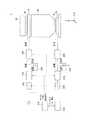
まず、本発明の第1実施形態に係るリソグラフィ装置について説明する。以下、本実施形態に係るリソグラフィ装置は、一例として、露光装置であるものとして説明する。図1は、本実施形態に係る露光装置1の構成を示す概略図である。露光装置1は、半導体デバイスの製造工程に使用され、ステップ・アンド・スキャン方式にて、レチクルRに形成されているパターンをウエハW上(基板上)に転写する投影型露光装置とする。露光装置1は、まず、照明系30と、レチクルRを保持するレチクルステージ10と、投影光学系40と、ウエハWを保持するウエハステージ20と、制御部300とを備える。なお、図1では、投影光学系40の光軸(本実施形態では鉛直方向)に平行にZ軸を取り、Z軸に垂直な平面内で露光時のレチクルRおよびウエハWの走査方向にX軸を取り、X軸に直交する非走査方向にY軸を取っている。(First embodiment)
First, a lithographic apparatus according to a first embodiment of the invention will be described. Hereinafter, the lithography apparatus according to the present embodiment will be described as an exposure apparatus as an example. FIG. 1 is a schematic diagram showing a configuration of an
照明系30は、不図示の光源から照射された光を調整し、レチクルRを照明する。レチクルRは、ウエハW上に転写されるべきパターン(例えば回路パターン)が形成された、例えば石英ガラス製の原版である。レチクルステージ(原版保持部)10は、レチクルRを保持しつつ、例えばXYの各軸方向に移動可能である。投影光学系40は、照明系30からの光で照明されたレチクルR上のパターンの像を所定の倍率(例えば1/2〜1/5)でウエハW上に投影する。ウエハWは、表面上にレジスト(感光剤)が塗布された、例えば単結晶シリコンからなる基板である。ウエハステージ(基板保持部)20は、不図示のチャックを介してウエハWを例えば真空吸着により保持しつつ、例えばXYZの各軸方向に移動可能である。ここで、レチクルステージ10とウエハステージ20とは、それぞれ、駆動部としてリニアモーターを採用し得る。リニアモーターは、移動体を、空圧または磁力などで浮上させた上で、ローレンツ力により発生される推力により移動させる。なお、レチクルステージ10とウエハステージ20との走査移動中、両者の位置は、それぞれ不図示の各レーザー干渉計を用いて継続的に検出される。制御部300は、各レーザー干渉計からの位置情報に基づいて、後述するレチクルステージ10とウエハステージ20との各ドライバー100、200に対し、駆動指令を送信する。これにより、制御部300は、両者の走査開始位置を正確に同期させるととも、定速走査領域での走査速度を高精度で制御し得る。 The
制御部300は、露光装置1の各構成要素の動作制御や演算処理などを実行し得る。制御部300は、例えばコンピューターなどで構成され、露光装置1の各構成要素に回線を介して接続されて、一のシーケンスに従って各構成要素の制御を実行し得る。露光装置1は、オペレーターが操作するインターフェースであり、制御部300に回線を介して接続されたシステムコンソール310を備える。特に、制御部300からのレチクルステージ10とウエハステージ20とへの駆動指令は、システムコンソール310に入力された、露光プロセスに沿ったジョブ条件により決定される。なお、制御部300、またはシステムコンソール310は、露光装置1の他の部分と一体で(共通の筐体内に)構成してもよいし、露光装置1の他の部分とは別体で(別の筐体内に)構成してもよい。 The
また、露光装置1は、レチクルステージ10用の駆動系として、第1ドライバー100と、第1電源110と、第1スイッチ140とを備える。同様に、露光装置1は、ウエハステージ20用の駆動系として、第2ドライバー200と、第2電源210と、第2スイッチ240とを備える。特に露光中、レチクルステージ10は、第1ドライバー100からの給電(電力供給)を受け、一方、ウエハステージ20は、第2ドライバー200からの給電に受けて、互いに同期されて走査移動する。ここで、第1電源110は、第1ドライバー100へ給電するものであり、一方、第2電源210は、第2ドライバー200へ給電するものである。また、切換部としての第1スイッチ140と第2スイッチ240とは、それぞれ制御部300の制御に基づいて、各電源110、120のON/OFFと、各電源への給電のON/OFFとを切り替える。 The
近年、生産性の観点から、レチクルステージおよびウエハステージの加速度および走査速度を増加させる傾向にある。リニアモーターの発生推力は、駆動電流に比例することから、各ステージを高速駆動させるためには、各ドライバーは、特に加速および減速時にリニアモーターへ多量の電力を供給しなければならない。特に各ステージの加速区間では、各ドライバーの電源電力でドライバーで消費する電力を賄う必要がある。これに対して、各ステージの等速区間では、推力をほとんど必要としないため、電力消費はほとんどないが、減速区間では、各ステージの走査速度やコイルの抵抗分に比例した逆起電圧が発生するため、回生電力が電源に戻る。すなわち、装置電力(露光装置1の全消費電力)については、各ステージの加速時にピーク電力が発生し、減速時にピーク電力が戻る。そこで、本実施形態では、露光装置1は、第1ドライバー100と第1電源110との間に、第1電源110からの充電に加え、レチクルステージ10の減速時における回生電力を充電可能とする大容量の第1キャパシター120を備える。同様に、露光装置1は、第2ドライバー200と第2電源210との間に、第2電源210からの充電に加え、ウエハステージ20の減速時における回生電力を充電可能とする大容量の第2キャパシター220を備える。そして、露光装置1は、以下に示すように、各キャパシター120、220を利用して、最も電力を必要とする各ステージの加速時の電源容量をカバーする。 In recent years, from the viewpoint of productivity, there is a tendency to increase the acceleration and scanning speed of the reticle stage and wafer stage. Since the thrust generated by the linear motor is proportional to the drive current, each driver must supply a large amount of electric power to the linear motor, particularly during acceleration and deceleration, in order to drive each stage at high speed. In particular, in the acceleration section of each stage, it is necessary to cover the power consumed by the driver with the power source power of each driver. In contrast, almost no thrust is required in the constant speed section of each stage, so there is almost no power consumption. However, in the deceleration section, a counter electromotive voltage proportional to the scanning speed of each stage and the resistance of the coil is generated. Therefore, the regenerative power returns to the power source. That is, with respect to the apparatus power (total power consumption of the exposure apparatus 1), peak power is generated during acceleration of each stage, and peak power returns during deceleration. Therefore, in the present embodiment, the
次に、露光装置1における駆動系ユニット、特にここでは一例として各ステージ装置の駆動と、その駆動系の電力供給(電力供給方法)について説明する。図2は、本実施形態における、全体的な処理の流れに合わせたステージ駆動系の駆動制御の流れを示すフローチャートである。なお、ここでは、露光装置1によるウエハWに対する露光処理は、おおむね25枚のウエハWを1ロットとして扱い、一のシーケンス(各駆動部の駆動条件を含む)に予め設定された露光ジョブに従って連続的に行われるものとする。まず、オペレーターによるシステムコンソール310の操作(露光装置1の電源ON)により露光装置1の稼働を開始すると、制御部300は、各ドライバー100、200、各電源110、210、各スイッチ140、240をONとする(ステップS100)。次に、制御部300は、レチクルステージ10およびウエハステージ20の初期位置駆動を実施させる(ステップS110)。次に、制御部300は、露光装置1を待機状態とする(ステップS120)。 Next, driving of the drive system unit in the
次に、制御部300は、オペレーターによるシステムコンソール310の操作(ジョブスタート指令)に基づいて、ウエハWへの露光(露光ジョブ、またはロット単位の処理)を開始させる。まず、制御部300は、露光を開始するにあたり、露光ジョブ、またはロット単位の処理が継続中かどうかを判断する(ステップS130)。ここで、制御部300は、継続中であると判断した場合には(Yes)、以下の動作を実施させる。まず、不図示のウエハ搬送システムに、ウエハキャリアにセッティングされているウエハWを1枚ずつ取り出させ、位置合わせを行わせた後、そのウエハWをウエハステージ20のチャック上へ搬送させる。次に、制御部300は、ウエハWをチャックに保持させ、前回のプロセス時に予め形成されているウエハW上の複数のアライメントマークを、順次、不図示の顕微鏡(アライメント計測系)により位置計測させる。そして、制御部300は、顕微鏡から得られた位置計測結果に基づいて、パターンの位置ずれ、回転ずれや倍率の変化などを求め、実際の露光前に適宜補正させる。 Next, the
その後、制御部300は、ウエハステージ20を移動させ、ウエハW上の複数のショット(パターン形成領域)の最初の露光位置に露光光を照射させ、各ステージ10、20のステップ移動、および露光光照射を連続的に実施させる(ステップS140)。このとき、制御部300は、ステップS140の間で、実際に露光中か、すなわち実際にステップ移動および露光光照射を実施しているかどうかを常時判断する。ここで、制御部300は、実際に露光中であると判断している特定の期間では(Yes)、第1電源110、または第1スイッチ140をOFFし、第1ドライバー100と第1キャパシター120への給電を停止させる(ステップS150:第1の工程)。このとき、レチクルステージ10は、第1キャパシター120に蓄えられている電荷と、レチクルステージ10の減速時に発生する回生電力とにより駆動される。一方、ステップS140にて、制御部300は、露光中ではないと判断している特定の期間は(No)、第2電源210、または第2スイッチ240をOFFし、第2キャパシター220への給電を停止させる(ステップS160:第2の工程)。ここで、露光中ではない期間とは、例えば、ウエハWの交換時などである。このとき、ウエハステージ20は、第2キャパシター220に蓄えられている電荷と、ウエハステージ20の減速時に発生する回生電力により駆動される。同時に、制御部300は、第1電源110または第1スイッチ140をONとすることで、レチクルステージ10のステップ移動および露光光照射を行っていた期間に電力を消費した第1キャパシター120への充電を行う。制御部300は、これらの工程を、ステップS130にて、露光ジョブ、またはロット単位の処理が継続されていない(No)と判断するまで繰り返す。 Thereafter, the
そして、制御部300は、ステップS130にて、露光ジョブ、またはロット単位の処理が継続されていないと判断した場合には(No)、各電源110、120、および各スイッチ140、240をONとする(ステップS170)。これにより、露光装置1は、次のジョブ指令もしくは次のロットまで待機状態となる(一旦、一連の処理を終了する)。 If the
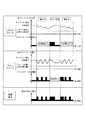
図3は、第1実施形態における第1キャパシター120および第2キャパシター220の各電圧および各消費電力の推移を示すグラフである。まず、図2のステップS150での実際に各ステージ10、20のステップ移動および露光光照射を実施している期間(図3で「露光中」と表記している)では、第1電源110および第1キャパシター120への給電が停止される。そのため、レチクルステージ10の駆動による装置電力(設備電力)の消費は発生しない。また、レチクルステージ10の加速時には、必要な消費電力は、第1キャパシター120に蓄えられている電荷により賄うため、キャパシター電圧が減少する。これに対して、レチクルステージ10の減速時には、減速による回生電力を第1キャパシター120へ充電するため、キャパシター電圧が上昇する。このような加減速を繰り返しながら、第1キャパシター120の電圧が徐々に減少していく。そして、この間のウエハステージ20の駆動に必要な消費電力は、装置電力が賄う。 FIG. 3 is a graph showing the transition of each voltage and each power consumption of the
一方、図2のステップS160での実際に各ステージ10、20のステップ移動および露光光照射を実施していない期間(図3で「ウエハ交換」と表記している)では、第2電源210および第2キャパシター220への給電が停止される。そのため、ウエハステージ20の駆動による装置電力の消費は発生しない。同時に、レチクルステージ10の第1電源110および第1スイッチ140のONにより、レチクルステージ10のステップ移動および露光光照射を行っていた期間の消費電力分が、装置電力から第1キャパシター120へ充電される。 On the other hand, during the period in which the stage movement of each
図9は、比較のための従来例として、本実施形態におけるステージ駆動系の動作および電力供給を実施しない場合の各ステージ駆動用のキャパシターの各電圧および各消費電力の推移を示すグラフである。本実施形態によらないならば、図9に示すように、レチクルステージとウエハステージとのピーク電力が重なってしまい、装置電力のピークが大きくなってしまうことがわかる。このように、露光装置1は、特にステージ駆動系に関して装置電力からの給電タイミングを上記のように適切に調整することで、露光装置1のピーク電力を低減することができる。このピーク電力を低減することができるということは、結果的に各電源110、210の大型化を避けることができる上でも望ましい。 FIG. 9 is a graph showing, as a conventional example for comparison, the transition of each voltage and power consumption of each stage driving capacitor when the operation of the stage driving system and the power supply in this embodiment are not performed. If not according to the present embodiment, as shown in FIG. 9, it can be seen that the peak power of the reticle stage and the wafer stage overlap, and the peak of the apparatus power increases. Thus, the
次に、第1キャパシター120および第2キャパシター220に設定し得るキャパシター容量について説明する。図4は、第1キャパシター120および第2キャパシター220に適用し得るキャパシター410を含む回路400を示す概念図である。回路400において、リニアモーター負荷430の負荷電流は、ドライバー420から供給されるものであり、ドライバー420は、キャパシター410から給電される。ここで、キャパシター410からドライバー420への供給電圧をVIN、供給電流をIINとし、ドライバー420からリニアモーター負荷430への負荷電流をIL、リニアモーター負荷430に発生したモーター電圧をVLとする。Next, capacitor capacities that can be set for the
図5は、リソグラフィ装置(例えば露光装置1)におけるリニアモーター負荷430の電流・電圧・電力の各推移を示すグラフである。リニアモーター負荷430を受けて駆動するスキャンステージは、加速開始時間T1(s)と加速終了時間T2(s)との間の加速を経て、最高速度に達した後にスキャン移動し、減速開始時間T3(s)と減速終了時間T4(s)との間の減速を経て停止する。ドライバー420は、この駆動の加速時と減速時について短時間でスキャンステージの大推力を得るために、大電流を必要とする。一方、スキャンステージのスキャン移動(スキャン露光)時には、等速運動のためほとんど電流を消費しないが、リニアモーターが最高速度で駆動するときに発生する逆起電圧が最大となるので、これを補う必要がある。すなわち、ドライバー420のハイサイドスイッチングONデューティーをDとすると、モーター最大電圧VL(max)と、ハイサイド側の電源電圧(初期のキャパシター間電圧)VINとの関係は、式(1)に示す条件を満たさなければならない。FIG. 5 is a graph showing changes in current, voltage, and power of the

一方、スキャンステージ加速時のドライバーの消費電力P1は、ドライバー効率をηとすると、式(2)のように、モーター電力とドライバー損失との和で表せる。 On the other hand, the power consumption P1 of the driver at the time of acceleration of the scan stage can be expressed by the sum of the motor power and the driver loss as shown in Expression (2), where η is the driver efficiency.
この電力をキャパシター410がすべて補うと仮定した場合、キャパシター容量をCとすると、電源電圧VINの電圧降下分ΔVIN1は、P=1/2×CV2から、式(3)で表される。Assuming that the
そして、式(1)および式(3)より、1回のスキャン移動に必要な加速時のキャパシター容量は、式(4)で表される。 From the equations (1) and (3), the capacitor capacity at the time of acceleration necessary for one scan movement is represented by the equation (4).
また、ドライバー420は、スキャンステージ加速時にはリニアモーターへ電力を供給するのに対し、減速時においては、リニアモーターで逆起電力が発生するので、回生電力がドライバー420へ戻る。ドライバー420に戻った電力は、スイッチング素子を介してキャパシター410へ戻る。このときの消費電力P2は、式(5)で表される。 Further, the
ここで、スキャンステージ減速時には、回生電力が支配的なため、式(5)の結果は、マイナスで計算されることになる。この場合、電圧上昇分ΔVIN2は、P=1/2×CV2から、式(6)で表される。Here, since the regenerative power is dominant when the scan stage is decelerated, the result of equation (5) is calculated as a negative value. In this case, the voltage increase ΔVIN2 is expressed by Equation (6) from P =½ × CV2 .
そして、式(3)および式(6)より、1回のスキャン移動でのキャパシター電圧ΔVINは、式(7)のように近似できる。From the equations (3) and (6), the capacitor voltage ΔVIN in one scan movement can be approximated as in the equation (7).
したがって、ドライバー420への給電をOFFしてからn回のスキャン移動を行う際に必要なキャパシター容量Cは、式(4)および式(7)より、式(8)で表される。 Therefore, the capacitor capacity C required when n times of scanning movement is performed after the power supply to the
なお、スキャンステージのスキャン移動中(すなわち等速時)でも、サーボがかかっているので、リニアモーターへ流れる電流はゼロではなく、ドライバー420の消費電力が発生する。ただし、この消費電力は、加速時および減速時と比べれば、かなり低く、式(8)の条件にあまり効いてこない電力量ではあるが、この条件も考慮して、多少マージンを持たせてキャパシター容量Cを設定(構成)するのが望ましい。 Even during the scanning movement of the scanning stage (that is, at constant speed), the servo is applied, so that the current flowing to the linear motor is not zero, and the power consumption of the
特に、本実施形態に係るリソグラフィ装置が、半導体露光装置や液晶露光装置のような大型の露光装置である場合には、キャパシター容量Cは、数十F(ファラド)程度必要となる。そして、このキャパシターとしては、電気二重層のようなエネルギー密度の高いものを用いることが望ましい。一方、大容量のキャパシターを必要としないリソグラフィ装置であれば、例えば、内部抵抗が小さく、充放電特性が優れているアルミ電解キャパシターを採用してもよい。また、近年の電気二重層キャパシターは、内部抵抗が1Ω程度と小さく、低損失の傾向にあるのに対し、大容量のスイッチング電源の効率は、0.7〜0.8程度で、2〜3割の損失が発生する。したがって、本実施形態のように最も電力を必要とするタイミングで各電源110、210のスイッチングを停止し、各キャパシター120、220のみで電力を供給することは、リソグラフィ装置全体の省エネルギー化を実現できる。 In particular, when the lithography apparatus according to the present embodiment is a large exposure apparatus such as a semiconductor exposure apparatus or a liquid crystal exposure apparatus, the capacitor capacitance C needs to be about several tens of F (farads). And as this capacitor, it is desirable to use a capacitor having a high energy density such as an electric double layer. On the other hand, if the lithography apparatus does not require a large-capacity capacitor, for example, an aluminum electrolytic capacitor having a small internal resistance and excellent charge / discharge characteristics may be employed. In recent years, an electric double layer capacitor has a low internal loss of about 1Ω and tends to have a low loss, whereas the efficiency of a large-capacity switching power supply is about 0.7 to 0.8, 2 to 3 A loss of 20% occurs. Therefore, the switching of the power supplies 110 and 210 is stopped at the timing that requires the most power as in the present embodiment, and the power is supplied only by the
以上のように、本実施形態によれば、それぞれ装置電源から電力が供給されて、同期して駆動する複数の駆動部を有する場合に、装置のピーク電力を低減するのに有利なリソグラフィ装置を提供することができる。 As described above, according to the present embodiment, a lithographic apparatus that is advantageous in reducing the peak power of the apparatus when the apparatus power supply is supplied from the apparatus power source and the plurality of driving units are driven in synchronization with each other. Can be provided.
(第2実施形態)
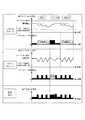
次に、本発明の第2実施形態に係るリソグラフィ装置について説明する。図6は、本実施形態に係る露光装置500の構成を示す概略図である。露光装置500の特徴は、第1実施形態に係る露光装置1に対して、さらに、制御部300が、各キャパシター120、220のキャパシター電圧に基づいて、各電源110、210または各スイッチ140、240のON/OFFを制御する点にある。特に、露光装置500は、複数のキャパシターのそれぞれに対応した複数の電圧計を有する。具体的には、第1電圧計510は、第1キャパシター120のキャパシター電圧を計測するものであり、一方、第2電圧計520は、第2キャパシター220のキャパシター電圧を計測するものであり、それぞれ、制御部300に信号配線を介して接続されている。なお、露光装置500の各構成要素には、露光装置1の各構成要素と対応するものについては同一の符号を付す。(Second Embodiment)
Next, a lithographic apparatus according to a second embodiment of the invention will be described. FIG. 6 is a schematic view showing the arrangement of the
図7は、本実施形態における、全体的な処理の流れに合わせたステージ駆動系の動作制御の流れを示すフローチャートである。この図7において、ステップS100からS150まで、およびステップS170は、第1実施形態における図2に示す工程とそれぞれ同様である。特に、図7での以下の工程では、制御部300は、ステップS140にて露光中ではないと判断している間は(No)、第1キャパシター120のキャパシター電圧が第1電源110の出力電圧未満かどうかを判断する(ステップS200)。ここで、制御部300は、出力電圧未満であると判断した場合には(Yes)、図2におけるステップS160と同様に、第1電源110または第1スイッチ140をONとし、同時に、第2電源210または第2スイッチ240をOFFとする(ステップS210)。このステップS210の工程は、制御部300がステップS200にて出力電圧を超える(No)と判断するまで維持する。そして、制御部300は、ステップS200にて出力電圧を超えると判断した場合には(No)、各電源110、210および各スイッチ140、240をONとする(ステップS220)。これらステップS140、および、S150またはS200からS220までの工程は、露光ジョブ、またはロット単位の処理が継続されている間、繰り返される。 FIG. 7 is a flowchart showing the flow of operation control of the stage drive system in accordance with the overall processing flow in this embodiment. In FIG. 7, steps S100 to S150 and step S170 are the same as the steps shown in FIG. 2 in the first embodiment. In particular, in the following process in FIG. 7, while the
図8は、第2実施形態における第1キャパシター120および第2キャパシター220の各電圧および各消費電力の推移を示すグラフである。実際に各ステージ10、20のステップ移動および露光光照射を実施している期間(図8で「露光中」とある期間)については、第1実施形態における図3と同様である。特に、図7のステップS140にて、レチクルステージ10のステップ移動および露光光照射を行っていた期間では、第1キャパシター120の電荷を消費した分、キャパシター電圧が減少し、第1電源110の出力電圧未満となる。そこで、本実施形態では、ステップ移動および露光光照射を実施していない期間(図8で「ウエハ交換時」とある期間)で、かつ上記出力電圧未満となっている間は、制御部300は、図7のステップS210の工程を実行する。すなわち、制御部300は、レチクルステージ10側については、第1電源110および第1スイッチ140をONとし、第1キャパシター120への充電を行う。なお、このときのウエハステージ20側については、制御部300は、第2電源210および第2スイッチ240をOFFとして、給電を停止させる。そして、ステップ移動および露光光照射を実施していない期間で、第1キャパシター120のキャパシター電圧が第1電源110の出力電圧を超えたということは、第1キャパシター120への充電が完了したことを意味する。そこで、制御部300は、図7のステップS200で出力電圧を超えたと判断したら、図7のステップS220にて第2電源210および第2スイッチ240をONとする。これにより、ステップ移動および露光光照射を実施していない期間に、それを実施していた期間に消費したウエハステージ20の電力を充電して、次のステップ移動および露光光照射に向けて備えることができる。 FIG. 8 is a graph showing the transition of each voltage and each power consumption of the
このように、本実施形態によれば、第1実施形態と同様の効果を奏しつつ、様々な露光ジョブに応じて、より柔軟にリソグラフィ装置のピーク電力を削減することができる Thus, according to the present embodiment, the peak power of the lithography apparatus can be reduced more flexibly according to various exposure jobs while achieving the same effects as those of the first embodiment.
なお、上記各実施形態では、図3や図8を用いて例示したように、「露光中」と「ウエハ交換」の期間として、実際に露光を実施している期間と実施していない期間とに対して、厳密に、各駆動部における給電の停止が対応している。しかしながら、本発明は、これに限定されるものではない。例えば、装置電力側のピーク電力が増大しないように、すなわち、レチクルステージ10の消費電力のピークと、ウエハステージ20の消費電力のピークとが重ならないようにするのであれば、各ステージ10、20についての給電を停止する期間が重なってもよい。また、図3の例では、例えば「露光中」内の全期間で、レチクルステージ10について給電を停止することにしているが、上記のような条件を満たすのであれば、全期間を通して給電を停止させる必要はなく、その一部に給電を行う期間が含まれていてもよい。 In each of the above-described embodiments, as illustrated with reference to FIGS. 3 and 8, as the periods of “during exposure” and “wafer exchange”, a period in which exposure is actually performed and a period in which exposure is not performed On the other hand, strictly speaking, the stopping of power feeding in each drive unit corresponds. However, the present invention is not limited to this. For example, if the peak power on the apparatus power side is not increased, that is, if the peak of the power consumption of the
また、上記各実施形態では、レチクルステージ10とウエハステージ20との駆動部の動作および電力供給について説明したが、本発明は、これに限定されない。例えば、その他マスキングブレードやそれらのアクティブカウンターなどを同期駆動する駆動部についても同様に適用可能である。また、上記各実施形態では、ステージ駆動系を構成する要素として、ドライバー、電源、スイッチ、およびキャパシターを例示したが、上記のような駆動系の動作および電力供給を実現できるならば、それ以外の構成要素を含むものであっても構わない。例えば、上記各実施形態では、レチクルステージ10用の駆動系に対応した第1電源110と、ウエハステージ20用の駆動系に対応した第2電源210との2つ(複数)の電源を用いる構成としている。しかしながら、本発明は、これに限らず、例えば、電源を1つとして、その下流側で各駆動部の各ドライバーおよび各キャパシターに向かう間に各スイッチを設置する構成もあり得る。 In each of the above embodiments, the operation of the driving unit and the power supply of the
また、上記各実施形態では、リソグラフィ装置として露光装置を例示したが、それに限らず、同期駆動し得る複数の駆動部を備える他のリソグラフィ装置であってもよい。例えば、電子線のような荷電粒子線で基板(上の感光剤)に描画を行う描画装置であってもよく、または基板上のインプリント材を型(モールド)で成形(成型)して基板上にパターンを形成するインプリント装置などであってもよい。 In each of the above embodiments, the exposure apparatus is exemplified as the lithography apparatus. However, the present invention is not limited thereto, and other lithography apparatuses including a plurality of driving units that can be driven synchronously may be used. For example, it may be a drawing apparatus that performs drawing on a substrate (upper photosensitive agent) with a charged particle beam such as an electron beam, or an imprint material on the substrate is molded (molded) with a mold (mold). An imprint apparatus that forms a pattern thereon may also be used.
(物品の製造方法)
一実施形態に係る物品の製造方法は、例えば、半導体デバイスなどのマイクロデバイスや微細構造を有する素子などの物品を製造するのに好適である。当該製造方法は、物体(例えば、感光剤を表面に有する基板)上に上記のリソグラフィ装置を用いてパターン(例えば潜像パターン)を形成する工程と、該工程でパターンを形成された物体を処理する工程(例えば、現像工程)とを含み得る。さらに、該製造方法は、他の周知の工程(酸化、成膜、蒸着、ドーピング、平坦化、エッチング、レジスト剥離、ダイシング、ボンディング、パッケージングなど)を含み得る。本実施形態の物品の製造方法は、従来の方法に比べて、物品の性能・品質・生産性・生産コストの少なくとも1つにおいて有利である。(Product manufacturing method)
The method for manufacturing an article according to an embodiment is suitable for manufacturing an article such as a micro device such as a semiconductor device or an element having a fine structure. The manufacturing method includes a step of forming a pattern (for example, a latent image pattern) on an object (for example, a substrate having a photosensitive agent on the surface) by using the above-described lithography apparatus, and a processing of the object on which the pattern is formed in the step. (For example, a development step). Further, the manufacturing method may include other well-known steps (oxidation, film formation, vapor deposition, doping, planarization, etching, resist stripping, dicing, bonding, packaging, and the like). The method for manufacturing an article according to the present embodiment is advantageous in at least one of the performance, quality, productivity, and production cost of the article as compared with the conventional method.
以上、本発明の好ましい実施形態について説明したが、本発明は、これらの実施形態に限定されず、その要旨の範囲内で種々の変形または変更が可能である。 As mentioned above, although preferable embodiment of this invention was described, this invention is not limited to these embodiment, A various deformation | transformation or change is possible within the range of the summary.
1 露光装置
10 レチクルステージ
20 ウエハステージ
110 第1電源
120 第1キャパシター
140 第1スイッチ
210 第2電源
220 第2キャパシター
240 第2スイッチ
300 制御部
DESCRIPTION OF
Claims (8)
Translated fromJapanese前記複数の駆動部へ駆動に要する電力をそれぞれ供給する電源と、
前記電源から電力をそれぞれ充電可能な複数のキャパシターと、
前記電源からの電力を、前記駆動部および前記キャパシターに供給するか否かをそれぞれ切り替える複数の切換部と、
前記複数の切換部の切り替えを制御する制御部と、を有し、
前記制御部は、前記複数の駆動部のうちの少なくとも1つの駆動部については、前記同期駆動する期間の少なくとも一部で、一方、前記少なくとも1つの駆動部とは別の駆動部については、前記同期駆動しない期間の少なくとも一部で、それぞれ対応する前記駆動部および前記キャパシターへの電力の供給を停止させ、前記キャパシターに充電されている電力で駆動させる、
ことを特徴とするリソグラフィ装置。A lithographic apparatus having a plurality of driving units that are driven synchronously in a specific period included in one sequence,
A power source for supplying power required for driving to the plurality of driving units;
A plurality of capacitors each capable of charging power from the power source;
A plurality of switching units each switching whether to supply power from the power source to the drive unit and the capacitor;
A control unit that controls switching of the plurality of switching units,
The control unit is configured to at least a part of the synchronous drive period for at least one drive unit of the plurality of drive units, while for the drive unit different from the at least one drive unit, the In at least a part of a period during which synchronous driving is not performed, supply of power to the corresponding drive unit and the capacitor is stopped, and the capacitor is driven with power charged.
A lithographic apparatus, comprising:
前記制御部は、前記電圧計が計測した前記電圧の値に基づいて、前記駆動部および前記キャパシターへの電力の供給を停止させる当該駆動部を決定する、
ことを特徴とする請求項1または2に記載のリソグラフィ装置。Having a plurality of voltmeters for measuring the voltages of the plurality of capacitors,
The control unit determines the drive unit to stop the supply of power to the drive unit and the capacitor based on the voltage value measured by the voltmeter.
The lithographic apparatus according to claim 1, wherein the apparatus is a lithographic apparatus.
ことを特徴とする請求項4に記載のリソグラフィ装置。When the voltage measured by the voltmeter is less than the output voltage of the power supply for a drive unit different from the at least one drive unit in at least a part of the period in which the synchronous drive is not performed Stops the supply of power to the drive unit and the capacitor, and drives with the power charged in the capacitor,
The lithographic apparatus according to claim 4, wherein:
前記複数の駆動部は、前記原版を保持する原版保持部を移動させる駆動部と、前記基板を保持する基板保持部を移動させる駆動部とを含む、
ことを特徴とする請求項1ないし5のいずれか1項に記載のリソグラフィ装置。The lithography apparatus is an exposure apparatus that irradiates a pattern formed on an original plate with light and exposes an image of the pattern onto a substrate via a projection optical system,
The plurality of driving units include a driving unit that moves an original holding unit that holds the original, and a driving unit that moves a substrate holding unit that holds the substrate.
The lithographic apparatus according to claim 1, wherein the lithographic apparatus is a lithographic apparatus.
前記複数の駆動部のうちの少なくとも1つの駆動部について、前記同期駆動する期間の少なくとも一部で、それに対応する前記駆動部と、該駆動部に対応し、電源から電力を充電可能なキャパシターとへの電力の供給を停止させ、当該キャパシターに充電されている電力で駆動させる第1の工程と、
前記少なくとも1つの駆動部とは別の駆動部について、前記同期駆動しない期間の少なくとも一部で、それに対応する前記駆動部と、該駆動部に対応し、電源から電力を充電可能なキャパシターとへの電力の供給を停止させ、当該キャパシターに充電されている電力で駆動させる第2の工程と、
を含むことを特徴とする電力供給方法。A power supply method for supplying power required for driving to a plurality of driving units that are synchronously driven in a specific period included in one sequence,
For at least one of the plurality of driving units, the driving unit corresponding to at least a part of the synchronous driving period, and a capacitor corresponding to the driving unit and capable of charging power from a power source, A first step of stopping the supply of power to the capacitor and driving with the power charged in the capacitor;
For a drive unit different from the at least one drive unit, to at least a part of the period in which the synchronous drive is not performed, to the drive unit corresponding to the drive unit and a capacitor corresponding to the drive unit and capable of charging power from a power source A second step of stopping the supply of power and driving with the power charged in the capacitor;
A power supply method comprising:
前記工程で前記パターンを形成された基板を処理する工程と、を含む、
ことを特徴とする物品の製造方法。
Forming a pattern on a substrate using the lithographic apparatus according to claim 1;
Processing the substrate on which the pattern is formed in the step.
A method for manufacturing an article.
Priority Applications (2)
| Application Number | Priority Date | Filing Date | Title |
|---|---|---|---|
| JP2013215364AJP6355313B2 (en) | 2013-10-16 | 2013-10-16 | Lithographic apparatus, power supply method, and article manufacturing method |
| US14/512,529US9500964B2 (en) | 2013-10-16 | 2014-10-13 | Lithography apparatus, power supplying method, and article manufacturing method |
Applications Claiming Priority (1)
| Application Number | Priority Date | Filing Date | Title |
|---|---|---|---|
| JP2013215364AJP6355313B2 (en) | 2013-10-16 | 2013-10-16 | Lithographic apparatus, power supply method, and article manufacturing method |
Publications (2)
| Publication Number | Publication Date |
|---|---|
| JP2015079823Atrue JP2015079823A (en) | 2015-04-23 |
| JP6355313B2 JP6355313B2 (en) | 2018-07-11 |
Family
ID=52809399
Family Applications (1)
| Application Number | Title | Priority Date | Filing Date |
|---|---|---|---|
| JP2013215364AActiveJP6355313B2 (en) | 2013-10-16 | 2013-10-16 | Lithographic apparatus, power supply method, and article manufacturing method |
Country Status (2)
| Country | Link |
|---|---|
| US (1) | US9500964B2 (en) |
| JP (1) | JP6355313B2 (en) |
Cited By (2)
| Publication number | Priority date | Publication date | Assignee | Title |
|---|---|---|---|---|
| CN111386029A (en)* | 2020-02-20 | 2020-07-07 | 哈尔滨工业大学 | High-precision synchronous control method and system for double-drive motion platform |
| WO2024219342A1 (en)* | 2023-04-20 | 2024-10-24 | キヤノン株式会社 | Motor drive device, manufacturing device, and article manufacturing method |
Families Citing this family (3)
| Publication number | Priority date | Publication date | Assignee | Title |
|---|---|---|---|---|
| US8836041B2 (en)* | 2012-11-16 | 2014-09-16 | Stmicroelectronics, Inc. | Dual EPI CMOS integration for planar substrates |
| JP2020124010A (en)* | 2019-01-29 | 2020-08-13 | キヤノン株式会社 | Control device, exposure apparatus, and item production method |
| CN120276220B (en)* | 2025-06-12 | 2025-09-09 | 新毅东(北京)科技有限公司 | Control method and system for variable slit of lithography machine and lithography machine |
Citations (8)
| Publication number | Priority date | Publication date | Assignee | Title |
|---|---|---|---|---|
| JP2001258176A (en)* | 2000-03-13 | 2001-09-21 | Sanyo Electric Co Ltd | Power consumption control system |
| US6356340B1 (en)* | 1998-11-20 | 2002-03-12 | Advanced Micro Devices, Inc. | Piezo programmable reticle for EUV lithography |
| JP2002271992A (en)* | 2001-03-14 | 2002-09-20 | Internatl Business Mach Corp <Ibm> | Device and method for supplying power, electrical machinery and apparatus, and method for supplying power in electrical machinery and apparatus |
| JP2002369579A (en)* | 2001-06-01 | 2002-12-20 | Nikon Corp | Motor driving apparatus, stage apparatus, exposure apparatus, device manufactured by this exposure apparatus, and device manufacturing method |
| JP2003143762A (en)* | 2001-10-30 | 2003-05-16 | Canon Inc | Processing device and device control method |
| JP2004104018A (en)* | 2002-09-12 | 2004-04-02 | Canon Inc | Manufacturing system |
| JP2008061352A (en)* | 2006-08-30 | 2008-03-13 | Canon Inc | Electrical apparatus and image forming apparatus |
| JP2009222824A (en)* | 2008-03-14 | 2009-10-01 | Ricoh Co Ltd | Image forming apparatus |
Family Cites Families (3)
| Publication number | Priority date | Publication date | Assignee | Title |
|---|---|---|---|---|
| JPS60175351A (en)* | 1984-02-14 | 1985-09-09 | Nippon Telegr & Teleph Corp <Ntt> | X rays generation device and x rays exposure method |
| WO2006038510A1 (en)* | 2004-10-01 | 2006-04-13 | Kabushiki Kaisha Yaskawa Denki | Linear motor system |
| CN104035287B (en)* | 2013-03-05 | 2016-03-16 | 中芯国际集成电路制造(上海)有限公司 | Exposure device and exposure method thereof |
- 2013
- 2013-10-16JPJP2013215364Apatent/JP6355313B2/enactiveActive
- 2014
- 2014-10-13USUS14/512,529patent/US9500964B2/enactiveActive
Patent Citations (8)
| Publication number | Priority date | Publication date | Assignee | Title |
|---|---|---|---|---|
| US6356340B1 (en)* | 1998-11-20 | 2002-03-12 | Advanced Micro Devices, Inc. | Piezo programmable reticle for EUV lithography |
| JP2001258176A (en)* | 2000-03-13 | 2001-09-21 | Sanyo Electric Co Ltd | Power consumption control system |
| JP2002271992A (en)* | 2001-03-14 | 2002-09-20 | Internatl Business Mach Corp <Ibm> | Device and method for supplying power, electrical machinery and apparatus, and method for supplying power in electrical machinery and apparatus |
| JP2002369579A (en)* | 2001-06-01 | 2002-12-20 | Nikon Corp | Motor driving apparatus, stage apparatus, exposure apparatus, device manufactured by this exposure apparatus, and device manufacturing method |
| JP2003143762A (en)* | 2001-10-30 | 2003-05-16 | Canon Inc | Processing device and device control method |
| JP2004104018A (en)* | 2002-09-12 | 2004-04-02 | Canon Inc | Manufacturing system |
| JP2008061352A (en)* | 2006-08-30 | 2008-03-13 | Canon Inc | Electrical apparatus and image forming apparatus |
| JP2009222824A (en)* | 2008-03-14 | 2009-10-01 | Ricoh Co Ltd | Image forming apparatus |
Cited By (2)
| Publication number | Priority date | Publication date | Assignee | Title |
|---|---|---|---|---|
| CN111386029A (en)* | 2020-02-20 | 2020-07-07 | 哈尔滨工业大学 | High-precision synchronous control method and system for double-drive motion platform |
| WO2024219342A1 (en)* | 2023-04-20 | 2024-10-24 | キヤノン株式会社 | Motor drive device, manufacturing device, and article manufacturing method |
Also Published As
| Publication number | Publication date |
|---|---|
| JP6355313B2 (en) | 2018-07-11 |
| US20150103328A1 (en) | 2015-04-16 |
| US9500964B2 (en) | 2016-11-22 |
Similar Documents
| Publication | Publication Date | Title |
|---|---|---|
| JP6355313B2 (en) | Lithographic apparatus, power supply method, and article manufacturing method | |
| US7084534B2 (en) | Alignment stage apparatus | |
| US8497980B2 (en) | Holding apparatus, exposure apparatus, exposure method, and device manufacturing method | |
| US11381196B2 (en) | Stage driving apparatus, lithography apparatus, and method of manufacturing article | |
| US20010006763A1 (en) | Methods and apparatuses for substrate transporting, positioning, holding, and exposure processing, device manufacturing method and device | |
| JP2018054847A (en) | Mobile device, exposure apparatus, flat panel display manufacturing method, and device manufacturing method | |
| US20110008718A1 (en) | Substrate conveyance method and substrate conveyance device, exposure apparatus using same, and device manufacturing method | |
| CN112540511B (en) | Stage device, lithographic apparatus, and article manufacturing method | |
| JP2005086093A (en) | Exposure apparatus and method for controlling stage apparatus | |
| JP2004031024A (en) | Light generation apparatus, exposure apparatus, and device manufacturing method | |
| US20150103329A1 (en) | Stage apparatus, lithography apparatus, and article manufacturing method | |
| TW202223545A (en) | Exposing apparatus and method for manufacturing article | |
| JP7535027B2 (en) | DRIVE APPARATUS, LITHOGRAPHIC APPARATUS AND METHOD FOR MANUFACTURING ARTICLE - Patent application | |
| JP2001358055A (en) | Exposure apparatus and device manufacturing method | |
| JP2024166936A (en) | MOTOR DRIVE APPARATUS, POWER SUPPLY APPARATUS, POWER SUPPLY METHOD, POWER SUPPLY APPARATUS, LITHOGRAPHY APPARATUS, AND METHOD FOR MANUFACTURING ARTICLE | |
| JP7022527B2 (en) | Stage equipment, lithography equipment, and article manufacturing methods | |
| JP2025143148A (en) | Motor drive device, power supply system, stage device, lithography apparatus, and method for manufacturing an article | |
| JP2002369579A (en) | Motor driving apparatus, stage apparatus, exposure apparatus, device manufactured by this exposure apparatus, and device manufacturing method | |
| JP2005311259A (en) | Drive mechanism deterioration detection apparatus and method, and exposure apparatus | |
| JP2025532450A (en) | Method and apparatus for bonding substrates | |
| NL2025107A (en) | Lithographic apparatus and method for motor temperature control |
Legal Events
| Date | Code | Title | Description |
|---|---|---|---|
| A621 | Written request for application examination | Free format text:JAPANESE INTERMEDIATE CODE: A621 Effective date:20161013 | |
| A977 | Report on retrieval | Free format text:JAPANESE INTERMEDIATE CODE: A971007 Effective date:20170614 | |
| A131 | Notification of reasons for refusal | Free format text:JAPANESE INTERMEDIATE CODE: A131 Effective date:20170620 | |
| A521 | Request for written amendment filed | Free format text:JAPANESE INTERMEDIATE CODE: A523 Effective date:20170808 | |
| A131 | Notification of reasons for refusal | Free format text:JAPANESE INTERMEDIATE CODE: A131 Effective date:20171205 | |
| A521 | Request for written amendment filed | Free format text:JAPANESE INTERMEDIATE CODE: A523 Effective date:20180205 | |
| TRDD | Decision of grant or rejection written | ||
| A01 | Written decision to grant a patent or to grant a registration (utility model) | Free format text:JAPANESE INTERMEDIATE CODE: A01 Effective date:20180515 | |
| A61 | First payment of annual fees (during grant procedure) | Free format text:JAPANESE INTERMEDIATE CODE: A61 Effective date:20180612 | |
| R151 | Written notification of patent or utility model registration | Ref document number:6355313 Country of ref document:JP Free format text:JAPANESE INTERMEDIATE CODE: R151 |