JP2015079187A - Display device and display driver - Google Patents
Display device and display driverDownload PDFInfo
- Publication number
- JP2015079187A JP2015079187AJP2013217242AJP2013217242AJP2015079187AJP 2015079187 AJP2015079187 AJP 2015079187AJP 2013217242 AJP2013217242 AJP 2013217242AJP 2013217242 AJP2013217242 AJP 2013217242AJP 2015079187 AJP2015079187 AJP 2015079187A
- Authority
- JP
- Japan
- Prior art keywords
- display driver
- display
- reference voltage
- grayscale
- grayscale reference
- Prior art date
- Legal status (The legal status is an assumption and is not a legal conclusion. Google has not performed a legal analysis and makes no representation as to the accuracy of the status listed.)
- Pending
Links
- 238000004364calculation methodMethods0.000claimsdescription37
- 239000004065semiconductorSubstances0.000claimsdescription5
- 239000000758substrateSubstances0.000claimsdescription5
- 238000010586diagramMethods0.000description22
- 230000006870functionEffects0.000description8
- 238000000034methodMethods0.000description8
- 238000012545processingMethods0.000description7
- 101100102627Oscarella pearsei VIN1 geneProteins0.000description5
- 230000000694effectsEffects0.000description3
- 238000009966trimmingMethods0.000description3
- 230000005540biological transmissionEffects0.000description2
- 238000012937correctionMethods0.000description2
- 230000006866deteriorationEffects0.000description2
- 239000004973liquid crystal related substanceSubstances0.000description2
- 238000004519manufacturing processMethods0.000description2
- 238000012360testing methodMethods0.000description2
- 230000032683agingEffects0.000description1
- 238000004458analytical methodMethods0.000description1
- 238000006243chemical reactionMethods0.000description1
- 230000000295complement effectEffects0.000description1
- 230000003292diminished effectEffects0.000description1
- 238000005401electroluminescenceMethods0.000description1
- 238000005516engineering processMethods0.000description1
- 230000005669field effectEffects0.000description1
- 239000011521glassSubstances0.000description1
- 239000011159matrix materialSubstances0.000description1
- 230000000717retained effectEffects0.000description1
- 238000005070samplingMethods0.000description1
- 229910052710siliconInorganic materials0.000description1
- 239000010703siliconSubstances0.000description1
- 230000003068static effectEffects0.000description1
Images


Classifications
- G—PHYSICS
- G09—EDUCATION; CRYPTOGRAPHY; DISPLAY; ADVERTISING; SEALS
- G09G—ARRANGEMENTS OR CIRCUITS FOR CONTROL OF INDICATING DEVICES USING STATIC MEANS TO PRESENT VARIABLE INFORMATION
- G09G3/00—Control arrangements or circuits, of interest only in connection with visual indicators other than cathode-ray tubes
- G09G3/20—Control arrangements or circuits, of interest only in connection with visual indicators other than cathode-ray tubes for presentation of an assembly of a number of characters, e.g. a page, by composing the assembly by combination of individual elements arranged in a matrix no fixed position being assigned to or needed to be assigned to the individual characters or partial characters
- G09G3/34—Control arrangements or circuits, of interest only in connection with visual indicators other than cathode-ray tubes for presentation of an assembly of a number of characters, e.g. a page, by composing the assembly by combination of individual elements arranged in a matrix no fixed position being assigned to or needed to be assigned to the individual characters or partial characters by control of light from an independent source
- G09G3/36—Control arrangements or circuits, of interest only in connection with visual indicators other than cathode-ray tubes for presentation of an assembly of a number of characters, e.g. a page, by composing the assembly by combination of individual elements arranged in a matrix no fixed position being assigned to or needed to be assigned to the individual characters or partial characters by control of light from an independent source using liquid crystals
- G09G3/3611—Control of matrices with row and column drivers
- G09G3/3685—Details of drivers for data electrodes
- G09G3/3688—Details of drivers for data electrodes suitable for active matrices only
- G—PHYSICS
- G09—EDUCATION; CRYPTOGRAPHY; DISPLAY; ADVERTISING; SEALS
- G09G—ARRANGEMENTS OR CIRCUITS FOR CONTROL OF INDICATING DEVICES USING STATIC MEANS TO PRESENT VARIABLE INFORMATION
- G09G2310/00—Command of the display device
- G09G2310/02—Addressing, scanning or driving the display screen or processing steps related thereto
- G09G2310/0202—Addressing of scan or signal lines
- G09G2310/0221—Addressing of scan or signal lines with use of split matrices
- G—PHYSICS
- G09—EDUCATION; CRYPTOGRAPHY; DISPLAY; ADVERTISING; SEALS
- G09G—ARRANGEMENTS OR CIRCUITS FOR CONTROL OF INDICATING DEVICES USING STATIC MEANS TO PRESENT VARIABLE INFORMATION
- G09G2320/00—Control of display operating conditions
- G09G2320/02—Improving the quality of display appearance
- G09G2320/0271—Adjustment of the gradation levels within the range of the gradation scale, e.g. by redistribution or clipping
- G09G2320/0276—Adjustment of the gradation levels within the range of the gradation scale, e.g. by redistribution or clipping for the purpose of adaptation to the characteristics of a display device, i.e. gamma correction
- G—PHYSICS
- G09—EDUCATION; CRYPTOGRAPHY; DISPLAY; ADVERTISING; SEALS
- G09G—ARRANGEMENTS OR CIRCUITS FOR CONTROL OF INDICATING DEVICES USING STATIC MEANS TO PRESENT VARIABLE INFORMATION
- G09G2320/00—Control of display operating conditions
- G09G2320/06—Adjustment of display parameters
- G09G2320/0693—Calibration of display systems
- G—PHYSICS
- G09—EDUCATION; CRYPTOGRAPHY; DISPLAY; ADVERTISING; SEALS
- G09G—ARRANGEMENTS OR CIRCUITS FOR CONTROL OF INDICATING DEVICES USING STATIC MEANS TO PRESENT VARIABLE INFORMATION
- G09G3/00—Control arrangements or circuits, of interest only in connection with visual indicators other than cathode-ray tubes
- G09G3/20—Control arrangements or circuits, of interest only in connection with visual indicators other than cathode-ray tubes for presentation of an assembly of a number of characters, e.g. a page, by composing the assembly by combination of individual elements arranged in a matrix no fixed position being assigned to or needed to be assigned to the individual characters or partial characters
- G09G3/34—Control arrangements or circuits, of interest only in connection with visual indicators other than cathode-ray tubes for presentation of an assembly of a number of characters, e.g. a page, by composing the assembly by combination of individual elements arranged in a matrix no fixed position being assigned to or needed to be assigned to the individual characters or partial characters by control of light from an independent source
- G09G3/36—Control arrangements or circuits, of interest only in connection with visual indicators other than cathode-ray tubes for presentation of an assembly of a number of characters, e.g. a page, by composing the assembly by combination of individual elements arranged in a matrix no fixed position being assigned to or needed to be assigned to the individual characters or partial characters by control of light from an independent source using liquid crystals
- G09G3/3611—Control of matrices with row and column drivers
- G09G3/3696—Generation of voltages supplied to electrode drivers
Landscapes
- Engineering & Computer Science (AREA)
- Physics & Mathematics (AREA)
- Computer Hardware Design (AREA)
- General Physics & Mathematics (AREA)
- Theoretical Computer Science (AREA)
- Chemical & Material Sciences (AREA)
- Crystallography & Structural Chemistry (AREA)
- Control Of Indicators Other Than Cathode Ray Tubes (AREA)
- Liquid Crystal Display Device Control (AREA)
- Liquid Crystal (AREA)
Abstract
Description
Translated fromJapanese本発明は、表示装置およびそれに搭載される表示ドライバに関し、特に複数の表示ドライバIC(Integrated Circuit)を用いて高画質の表示を実現する表示装置に好適に利用できるものである。 The present invention relates to a display device and a display driver mounted thereon, and in particular, can be suitably used for a display device that realizes high-quality display using a plurality of display driver ICs (Integrated Circuits).
近年、ディスプレイの高解像度化、大型化が進んでいる。高解像度化、大型化が進むと1チップの表示ドライバで駆動することが困難となり、多チップ(マルチチップ)化が進む。このとき、複数の表示ドライバの間に出力電圧にばらつきがあると表示パネルの輝度差となるため、画質を劣化させるという、問題がある。 In recent years, the resolution and size of displays have been increasing. As resolution and size increase, it becomes difficult to drive with a single-chip display driver, and the number of chips increases. At this time, if there is a variation in the output voltage among the plurality of display drivers, there is a difference in luminance of the display panel.
特許文献1には、複数の駆動回路部品を連携させて1つの表示領域を駆動する液晶表示装置の表示品質の低下を防ぐ技術が開示されている。1つの駆動回路部品で生成した階調基準電圧に基づいて、他の駆動回路部品の階調基準電圧を生成する。ここで、階調基準電圧とは、駆動回路部品から表示パネルに出力される出力電圧を生成するための、複数の階調電圧を生成するときに基準となる電圧である。出力電圧は同じ階調基準電圧から生成されるので、ばらつきを抑えることができるとされる。
特許文献2には、マスターモードの表示ドライバとスレーブモードの表示ドライバとを備える表示装置において、各表示ドライバ間の電源電圧の降下を抑制して、表示品質の低下を防止する技術が開示されている。マスターモードの表示ドライバから、スレーブモードの表示ドライバに対して、複数の階調電圧を供給する。送出側と受信側それぞれにボルテージフォロワ回路を設けることにより、出力インピーダンスを下げ入力インピーダンスを上げることができるので、階調電圧は伝送経路での電圧降下をほとんど生じさせない。これにより、表示装置の画面におけるバイアスずれやブロックむらを防止して表示品質の低下を防止することができるとされる(同文献第14頁)。
特許文献1及び2について本発明者が検討した結果、以下のような新たな課題があることがわかった。 As a result of examination of
特許文献1に開示される表示装置においては、複数の駆動回路部品(表示ドライバ)の間で、階調基準電圧のみを受け渡して、複数の駆動回路部品の間での出力電圧のばらつきを抑えようとしている。階調基準電圧は、複数の階調電圧を生成するときに基準となる電圧であるが、1本のアナログ信号、即ち、1点の基準電位が複数の駆動回路部品の間で共有されるに留まる。複数の階調電圧は、共有された階調基準電圧に基づいて、それぞれの駆動回路部品で生成される。同文献の図9と第0143段落〜第0155段落に記載されるように、それぞれの駆動回路部品では、傾き調整と振幅調整を行うことにより所定のガンマ特性を持たせる補正を行う。階調基準電圧のみを共通化しても、仮にこのガンマ補正回路にばらつきがあれば、複数の駆動回路部品の間での出力電圧のばらつきを生じる恐れがある。 In the display device disclosed in
これに対して特許文献2に開示される表示装置においては、複数の階調電圧をマスター表示ドライバからスレーブ表示ドライバに供給することにより、当該複数の階調電圧の全てを等しい電圧に揃えることができる。 On the other hand, in the display device disclosed in
しかしながら、この場合は、複数の階調電圧を伝送する必要があるため、以下の問題が発生する。 However, in this case, since it is necessary to transmit a plurality of gradation voltages, the following problem occurs.
第1の課題は、表示パネルの基板上の配線が増えることである。階調電圧の本数は、表示データの階調数に依存するので、数10本から100本以上となる場合もあり、配線の占める面積の増加は小型化を妨げ、コスト上昇を招く恐れがある。 The first problem is that the wiring on the substrate of the display panel increases. Since the number of gradation voltages depends on the number of gradations of the display data, the number of gradation voltages may be several tens to 100 or more, and an increase in the area occupied by the wiring may hinder downsizing and increase the cost. .
第2の課題は、表示ドライバをICで実現した場合に、チップ面積が増大し、コスト上昇を招くことである。上述のように階調電圧の本数は多数に上るので、これを出力するためのマスター側のパッド数とこれを受信するためのスレーブ側のパッド数を増加させる。パッド数の増加はチップ面積を増大させ、コスト上昇を招く恐れがある。また、階調電圧の配線長が長い場合には、これを駆動するために十分な駆動能力を備える出力回路を多数備える必要がある。これも同様にチップ面積を増大させ、コスト上昇を招く恐れがある。 The second problem is that when the display driver is realized by an IC, the chip area increases and the cost increases. As described above, since the number of grayscale voltages increases, the number of pads on the master side for outputting them and the number of pads on the slave side for receiving them are increased. An increase in the number of pads increases the chip area and may increase the cost. Further, when the wiring length of the gradation voltage is long, it is necessary to provide a large number of output circuits having a sufficient driving capability for driving the gradation voltage. This also increases the chip area and may increase the cost.
第3の課題は、マスターからスレーブの表示ドライバに供給される階調電圧にノイズが混入すると、その影響がスレーブ側に及ぶので、階調電圧を共有した効果を減殺させ、表示品質の低下を招く恐れがあることである。この点は、特許文献1に記載される技術にも共通する課題である。 The third problem is that if noise is mixed in the grayscale voltage supplied from the master to the slave display driver, the effect will extend to the slave side, so the effect of sharing the grayscale voltage will be diminished and the display quality will be reduced. There is a risk of inviting. This is a problem common to the technique described in
本発明の目的は、表示ドライバのチップ面積の増大や、表示パネルの配線面積の増加を最小限に抑え、且つノイズ耐性を高く保ちながら、複数の表示ドライバ間での出力電圧のばらつきを抑えることである。 It is an object of the present invention to suppress variations in output voltage among a plurality of display drivers while minimizing an increase in chip area of a display driver and an increase in wiring area of a display panel and keeping noise resistance high. It is.
このような課題を解決するための手段を以下に説明するが、その他の課題と新規な特徴は、本明細書の記述及び添付図面から明らかになるであろう。 Means for solving such problems will be described below, but other problems and novel features will become apparent from the description of the present specification and the accompanying drawings.
一実施の形態によれば、下記の通りである。 According to one embodiment, it is as follows.
すなわち、表示データに基づいて、表示パネルの複数の領域の複数のソース線に階調信号を出力する、第1と第2の表示ドライバを含む複数の表示ドライバを備える表示装置であって、以下のように構成される。複数の表示ドライバのそれぞれは、表示データに対応する階調信号を生成するための複数のグレースケール基準電圧を生成可能であり、第1表示ドライバは、第2表示ドライバに対して、自己の生成した複数のグレースケール基準電圧を順次伝送可能に構成される。第2表示ドライバは、伝送されたグレースケール基準電圧に基づいて、第1表示ドライバと第2表示ドライバでそれぞれ生成されるグレースケール基準電圧の差の絶対値を小さくする較正を、第1表示ドライバに実行させ、または自身で実行する。ここで、複数のグレースケール基準電圧は、上述の複数の階調電圧そのものであっても良いし、複数の階調電圧に所望のガンマ特性を持たせるために供給される、複数の特徴点の基準電圧であってもよい。 That is, a display device including a plurality of display drivers including first and second display drivers that outputs gradation signals to a plurality of source lines in a plurality of regions of a display panel based on display data, It is configured as follows. Each of the plurality of display drivers can generate a plurality of gray scale reference voltages for generating gradation signals corresponding to the display data, and the first display driver generates itself for the second display driver. The plurality of gray scale reference voltages can be sequentially transmitted. The second display driver performs calibration to reduce the absolute value of the difference between the gray scale reference voltages generated by the first display driver and the second display driver based on the transmitted gray scale reference voltage. Or run on your own. Here, the plurality of gray scale reference voltages may be the plurality of gradation voltages themselves, or a plurality of feature points supplied to give the plurality of gradation voltages desired gamma characteristics. It may be a reference voltage.
前記一実施の形態によって得られる効果を簡単に説明すれば下記のとおりである。 The effect obtained by the one embodiment will be briefly described as follows.
すなわち、表示ドライバのチップ面積の増大や、表示パネルの配線面積の増加を最小限に抑え、且つノイズ耐性を高く保ちながら、複数の表示ドライバ間での出力電圧のばらつきを抑えることができる。 That is, it is possible to suppress variations in output voltage among a plurality of display drivers while minimizing an increase in the chip area of the display driver and an increase in the wiring area of the display panel and maintaining high noise resistance.
1.実施の形態の概要
先ず、本願において開示される代表的な実施の形態について概要を説明する。代表的な実施の形態についての概要説明で括弧を付して参照する図面中の参照符号はそれが付された構成要素の概念に含まれるものを例示するに過ぎない。1. First, an outline of a typical embodiment disclosed in the present application will be described. Reference numerals in the drawings referred to in parentheses in the outline description of the representative embodiments merely exemplify what are included in the concept of the components to which the reference numerals are attached.
〔1〕<複数の表示ドライバ間でグレースケール基準電圧を順次伝送する表示装置>
本発明の代表的な実施の形態に係る表示装置(100)は、表示データに基づいて、表示パネル(90)の複数のソース線(91_1)に階調信号を出力可能な第1表示ドライバ(1)と、前記表示パネルの他の複数のソース線(91_2)に階調信号を出力可能な第2表示ドライバ(2)とを備え、以下のように構成される。[1] <Display device that sequentially transmits grayscale reference voltage among a plurality of display drivers>
A display device (100) according to a representative embodiment of the present invention includes a first display driver that can output gradation signals to a plurality of source lines (91_1) of a display panel (90) based on display data. 1) and a second display driver (2) capable of outputting gradation signals to the other plurality of source lines (91_2) of the display panel, and is configured as follows.
前記第1表示ドライバと前記第2表示ドライバのそれぞれは、前記表示データに対応する階調信号を生成するための複数のグレースケール基準電圧を生成可能に構成される(7、8)。 Each of the first display driver and the second display driver is configured to be able to generate a plurality of gray scale reference voltages for generating a gradation signal corresponding to the display data (7, 8).
前記第1表示ドライバは、前記第2表示ドライバに対して、自己の生成した前記複数のグレースケール基準電圧を順次伝送可能に構成される(10、83)。 The first display driver is configured to sequentially transmit the plurality of gray scale reference voltages generated by the first display driver to the second display driver (10, 83).
前記第2表示ドライバは、前記順次伝送されたグレースケール基準電圧に基づいて、前記第1表示ドライバで生成されるグレースケール基準電圧と前記第2表示ドライバで生成されるグレースケール基準電圧との差の絶対値を小さくする較正を実行可能に構成される。 The second display driver determines a difference between a grayscale reference voltage generated by the first display driver and a grayscale reference voltage generated by the second display driver based on the sequentially transmitted grayscale reference voltages. It is configured to be able to perform calibration to reduce the absolute value of.
これにより、表示ドライバのチップ面積の増大や、表示パネルの配線面積の増加を最小限に抑え、且つノイズ耐性を高く保ちながら、複数の表示ドライバ間での出力電圧のばらつきを抑えることを可能とした、表示装置を提供することができる。 As a result, it is possible to minimize variations in output voltage among multiple display drivers while minimizing an increase in display driver chip area and display panel wiring area and maintaining high noise resistance. In addition, a display device can be provided.
〔2〕<第2表示ドライバ(マスター)で算出した較正値を第1表示ドライバ(スレーブ)に返送(図2)>
項1において、前記第2表示ドライバは、前記順次伝送されたグレースケール基準電圧と自己の生成した前記複数のグレースケール基準電圧のうちの対応するグレースケール基準電圧とを比較し、前記比較の結果に基づいて較正値を算出し(29)、前記較正値を前記第1表示ドライバに対して伝送可能に構成される(85、86)。[2] <Calibration value calculated by the second display driver (master) is returned to the first display driver (slave) (FIG. 2)>
In the first aspect, the second display driver compares the sequentially transmitted grayscale reference voltage with a corresponding grayscale reference voltage among the plurality of grayscale reference voltages generated by the second display driver. A calibration value is calculated on the basis of (29), and the calibration value can be transmitted to the first display driver (85, 86).
前記第1表示ドライバは伝送された前記較正値に基づいて、自己の生成するグレースケール基準電圧を変更可能に構成される(30)。 The first display driver is configured to change a grayscale reference voltage generated by the first display driver based on the transmitted calibration value (30).
これにより、マスター(第2)表示ドライバが較正値を算出し、スレーブ(第1)表示ドライバが自己の発生するグレースケール基準電圧をマスター側に一致させる方向に較正する、表示装置を提供することができる。スレーブ(第1)表示ドライバから順次伝送されたグレースケール基準電圧を、マスター(第2)表示ドライバが、自己が生成したグレースケール基準電圧と比較することによって算出した較正値を、スレーブ(第1)表示ドライバに返送することによって、スレーブ(第1)表示ドライバが自己の発生するグレースケール基準電圧をマスター側に一致させる方向に較正する。 Thus, a display device is provided in which a master (second) display driver calculates a calibration value, and a slave (first) display driver calibrates the grayscale reference voltage generated by itself to the master side. Can do. The calibration value calculated by the master (second) display driver comparing the grayscale reference voltage sequentially transmitted from the slave (first) display driver with the grayscale reference voltage generated by itself is used as the slave (first). ) By returning it to the display driver, the slave (first) display driver calibrates the grayscale reference voltage generated by itself to the master side.
〔3〕<複数のスレーブ(第3)表示ドライバ(図3)>
項2において、前記表示装置は、前記第1表示ドライバ(1_1)と前記第2表示ドライバ(2)が階調電圧を出力する複数のソース線(91_1、91_2)とは異なる、前記表示パネルの複数のソース線(91_3)に階調信号を出力可能な第3表示ドライバ(1_3)をさらに備える。[3] <Slave (third) display driver (FIG. 3)>
In the
前記第3表示ドライバは、前記表示データに対応する階調信号を生成するための複数のグレースケール基準電圧を生成可能に構成される(21_3)。 The third display driver is configured to be capable of generating a plurality of gray scale reference voltages for generating a gray scale signal corresponding to the display data (21_3).
前記第3表示ドライバは、前記第2表示ドライバに対して、自己の生成した前記複数のグレースケール基準電圧を順次伝送可能に構成される(22_3、83_3、84)。 The third display driver is configured to be able to sequentially transmit the plurality of gray scale reference voltages generated by itself to the second display driver (22_3, 83_3, 84).
前記第2表示ドライバは、前記順次伝送されたグレースケール基準電圧と自己の生成した前記複数のグレースケール基準電圧のうちの対応するグレースケール基準電圧とを比較し、前記比較の結果に基づいて較正値を算出し(29)、前記較正値を前記第3表示ドライバに対して伝送可能に構成される(85、86_3)。 The second display driver compares the sequentially transmitted grayscale reference voltage with a corresponding grayscale reference voltage among the plurality of grayscale reference voltages generated by the second display driver, and calibrates based on a result of the comparison. A value is calculated (29), and the calibration value is configured to be transmitted to the third display driver (85, 86_3).
前記第3表示ドライバは伝送された前記較正値に基づいて、自己の生成するグレースケール基準電圧を変更可能に構成される(30_3)。 The third display driver is configured to change a grayscale reference voltage generated by the third display driver based on the transmitted calibration value (30_3).
これにより、1個のマスター(第2)表示ドライバと複数個のスレーブ(第1、第3等)表示ドライバを備える表示装置において、表示ドライバのチップ面積の増大や、表示パネルの配線面積の増加を最小限に抑え、且つノイズ耐性を高く保ちながら、複数の表示ドライバ間での出力電圧のばらつきを抑えることができる。複数個のスレーブ(第1、第3等)表示ドライバは、マスター(第2)表示ドライバに対して、それぞれ順次自己が発生したグレースケール基準電圧をマスター側に送出し、マスターは順次較正値を算出してスレーブ側に返送する。返送されたスレーブ側は、返送された較正値に基づいて、自己が発生するグレースケール基準電圧を変更する。 Accordingly, in a display device including one master (second) display driver and a plurality of slave (first, third, etc.) display drivers, the chip area of the display driver is increased and the wiring area of the display panel is increased. It is possible to suppress variations in output voltage among a plurality of display drivers while minimizing noise and maintaining high noise resistance. A plurality of slave (first, third, etc.) display drivers sequentially send their own generated gray scale reference voltages to the master (second) display driver, and the master sequentially outputs calibration values. Calculate and send back to the slave side. The returned slave side changes the gray scale reference voltage generated by itself based on the returned calibration value.
〔4〕<第1表示ドライバ(マスター)から伝送されるグレースケール基準電圧を基準に、第2表示ドライバ(スレーブ)が自己較正(図4)>
項1において、前記第2表示ドライバは、前記順次伝送されたグレースケール基準電圧と自己の生成した前記複数のグレースケール基準電圧のうちの対応するグレースケール基準電圧とを比較し(29)、前記比較の結果に基づいて、自己の生成するグレースケール基準電圧を変更可能に構成される(30)。[4] <The second display driver (slave) performs self-calibration based on the gray scale reference voltage transmitted from the first display driver (master) (FIG. 4)>
In the
これにより、マスター(第1)表示ドライバから伝送されるグレースケール基準電圧を基準に、スレーブ(第2)表示ドライバが、自己の発生するグレースケール基準電圧をマスター側に一致させる方向に自律的に較正する、表示装置を提供することができる。スレーブ(第2)表示ドライバは、マスター(第1)表示ドライバから順次伝送されたグレースケール基準電圧を、自己が生成したグレースケール基準電圧と比較することによって、スレーブ(第2)表示ドライバが自己の発生するグレースケール基準電圧をマスター側に一致させる方向に較正する。 This allows the slave (second) display driver to autonomously move the gray scale reference voltage generated by the slave (second) display driver to the master side based on the gray scale reference voltage transmitted from the master (first) display driver. A display device can be provided for calibration. The slave (second) display driver compares the grayscale reference voltage sequentially transmitted from the master (first) display driver with the grayscale reference voltage generated by the slave (second) display driver. Is calibrated in the direction to match the gray scale reference voltage generated by
〔5〕<複数のスレーブ(第2、第4等)表示ドライバが並列に自己較正(図5)>
項4において、前記表示装置は、前記第1表示ドライバ(1)と前記第2表示ドライバ(2_2)が階調電圧を出力する複数のソース線(91_1、91_2)とは異なる、前記表示パネルの複数のソース線(91_3)に階調信号を出力可能な第4表示ドライバ(2_3)をさらに備える。[5] <Slave (second, fourth, etc.) display drivers self-calibrate in parallel (FIG. 5)>
In the
前記第4表示ドライバは、前記表示データに対応する階調信号を生成するための複数のグレースケール基準電圧を生成可能に構成される(21_3)。 The fourth display driver is configured to be capable of generating a plurality of gray scale reference voltages for generating a gradation signal corresponding to the display data (21_3).
前記第1表示ドライバは、前記第2表示ドライバと前記第4表示ドライバに対して並行して、自己の生成した前記複数のグレースケール基準電圧を順次伝送可能に構成される(83、84_2、84_3)。 The first display driver is configured to be capable of sequentially transmitting the plurality of grayscale reference voltages generated by the first display driver in parallel to the second display driver and the fourth display driver (83, 84_2, 84_3). ).
前記第2表示ドライバは、前記順次伝送されたグレースケール基準電圧と自己の生成した前記複数のグレースケール基準電圧のうちの対応するグレースケール基準電圧とを比較し(18_2)、前記比較の結果に基づいて、自己の生成するグレースケール基準電圧を変更可能に構成される(30_2)。 The second display driver compares the sequentially transmitted gray scale reference voltage with a corresponding gray scale reference voltage among the plurality of gray scale reference voltages generated by the second display driver (18_2), and determines the result of the comparison. Based on this, the gray scale reference voltage generated by itself can be changed (30_2).
前記第4表示ドライバも、同様に、前記順次伝送されたグレースケール基準電圧と自己の生成した前記複数のグレースケール基準電圧のうちの対応するグレースケール基準電圧とを比較し(18_3)、前記比較の結果に基づいて、自己の生成するグレースケール基準電圧を変更可能に構成される(30_3)。 Similarly, the fourth display driver compares the sequentially transmitted gray scale reference voltage with the corresponding gray scale reference voltage among the plurality of gray scale reference voltages generated by the fourth display driver (18_3). Based on the result, the grayscale reference voltage generated by itself can be changed (30_3).
これにより、1個のマスター(第1)表示ドライバと複数個のスレーブ(第2、第4等)表示ドライバを備える表示装置において、表示ドライバのチップ面積の増大や、表示パネルの配線面積の増加を最小限に抑え、且つノイズ耐性を高く保ちながら、複数の表示ドライバ間での出力電圧のばらつきを抑えることができる。マスター(第1)表示ドライバは、複数個のスレーブ(第2、第4等)表示ドライバに対して並行に、自己が発生した複数のグレースケール基準電圧を順次送出し、複数個のスレーブ(第2、第4等)表示ドライバは、それぞれ、自己が発生するグレースケール基準電圧を受信したグレースケール基準電圧に近づける制御を行う。 Accordingly, in a display device including one master (first) display driver and a plurality of slave (second, fourth, etc.) display drivers, the chip area of the display driver and the wiring area of the display panel are increased. It is possible to suppress variations in output voltage among a plurality of display drivers while minimizing noise and maintaining high noise resistance. The master (first) display driver sequentially sends a plurality of grayscale reference voltages generated by the master (first) display driver in parallel to a plurality of slave (second, fourth, etc.) display drivers. (2, 4th, etc.) Each display driver controls the grayscale reference voltage generated by itself to be close to the received grayscale reference voltage.
〔6〕<ディジタル較正(図6〜9)>
項1から項5のうちのいずれか1項において、前記第2表示ドライバは、アナログ/ディジタル変換器(13)と、記憶回路(17)と、演算回路(18)とを備え、以下のように構成される。[6] <Digital calibration (FIGS. 6-9)>
In any one of
前記アナログ/ディジタル変換器は、前記第2表示ドライバが生成したグレースケール基準電圧と前記順次伝送されたグレースケール基準電圧とをそれぞれ随時ディジタル値に変換可能であり、前記記憶回路は、前記ディジタル値を記憶可能であり、前記演算回路は、前記記憶回路に記憶されたディジタル値を読み出して比較及び/または除算を実行することにより、前記較正を実行可能に構成される。 The analog / digital converter can convert the grayscale reference voltage generated by the second display driver and the sequentially transmitted grayscale reference voltage into digital values as needed, and the storage circuit can convert the digital value. And the arithmetic circuit is configured to perform the calibration by reading the digital value stored in the storage circuit and performing comparison and / or division.
これにより、グレースケール基準電圧を受信した側である、第2表示ドライバにおいて、ディジタル処理によって、項2と項3の場合には較正値を算出し、または、項4と項5の場合には自己のグレースケール電圧を較正することができる。 Thus, in the second display driver on the side receiving the gray scale reference voltage, the calibration value is calculated in the case of the
〔7〕<アナログ較正(図10〜13)>
項1から項5のうちのいずれか1項において、前記第2表示ドライバは、アナログ比較器(14)と、記憶回路(17)と、演算回路(19)とを備え、以下のように構成される。[7] <Analog calibration (FIGS. 10 to 13)>
In any one of
前記アナログ比較器は、前記第2表示ドライバが生成したグレースケール基準電圧と前記伝送されたグレースケール基準電圧とをそれぞれ随比較可能であり、前記記憶回路は、前記比較結果を記憶可能であり、前記演算回路は、前記記憶回路に記憶された比較結果を読み出して演算を実行することにより、前記較正を実行可能に構成される。 The analog comparator can compare the grayscale reference voltage generated by the second display driver with the transmitted grayscale reference voltage, and the storage circuit can store the comparison result, The arithmetic circuit is configured to execute the calibration by reading the comparison result stored in the storage circuit and executing the calculation.
これにより、グレースケール基準電圧を受信した側である、第2表示ドライバにおいて、ディジタル処理によって、項2と項3の場合には較正値を算出し、または、項4と項5の場合には自己のグレースケール電圧を較正することができる。 Thus, in the second display driver on the side receiving the gray scale reference voltage, the calibration value is calculated in the case of the
〔8〕<アナログ比較器のオフセットキャンセル(図11)>
項7において、前記第2表示ドライバは、前記アナログ比較器の入力を相互に入れ替えることができるスイッチ(15)をさらに備える。[8] <Analog comparator offset cancellation (FIG. 11)>
In
前記アナログ比較器の一方の入力端子に前記第2表示ドライバが生成したグレースケール基準電圧が入力され、前記アナログ比較器の他方の入力端子に前記伝送されたグレースケール基準電圧が入力された場合の、第1比較結果が前記記憶回路に格納される。 When the grayscale reference voltage generated by the second display driver is input to one input terminal of the analog comparator and the transmitted grayscale reference voltage is input to the other input terminal of the analog comparator. The first comparison result is stored in the storage circuit.
前記スイッチを切り替えることにより、前記アナログ比較器の前記一方の入力端子に前記伝送されたグレースケール基準電圧が入力され、前記アナログ比較器の前記他方の入力端子に前記第2表示ドライバが生成したグレースケール基準電圧が入力され、そのときの、第2比較結果が前記記憶回路に格納される。 By switching the switch, the transmitted grayscale reference voltage is input to the one input terminal of the analog comparator, and the second display driver generates the gray display reference voltage generated to the other input terminal of the analog comparator. The scale reference voltage is input, and the second comparison result at that time is stored in the storage circuit.
前記演算回路は、前記第1比較結果と前記第2比較結果に基づいて、前記較正を実行可能に構成される。 The arithmetic circuit is configured to be able to execute the calibration based on the first comparison result and the second comparison result.
これにより、アナログ比較器の入力オフセットを相殺する演算を、前記演算回路に実行させ、前記較正をより正確に実行することができる。 As a result, it is possible to cause the arithmetic circuit to execute an operation for canceling the input offset of the analog comparator, and to execute the calibration more accurately.
〔9〕<電源投入時に較正>
項1から項8のうちのいずれか1項において、前記較正は、電源投入時に実行可能に構成される。[9] <Calibration at power-on>
これにより、経年変化に対応した較正を実行することができる。 Thereby, the calibration corresponding to a secular change can be performed.
〔10〕<表示の帰線期間に較正>
項9項において、前記較正は、さらに表示の帰線期間に実行可能に構成される。[10] <Calibration during display blanking period>
In
これにより、表示中に逐次、較正を実行することができる。 Thereby, calibration can be executed sequentially during display.
〔11〕<較正結果を保持する不揮発性メモリ>
項1から項8のうちのいずれか1項において、前記較正の結果を保持可能な不揮発性メモリを備える。[11] <Nonvolatile memory holding calibration results>
これにより、表示装置の出荷試験において較正を実行、その結果を保持し、出荷時に較正されたグレースケール基準電圧を、出荷後に再現させることができる。 Thus, calibration can be executed in the shipping test of the display device, the result can be retained, and the grayscale reference voltage calibrated at the time of shipping can be reproduced after shipping.
〔12〕<第1表示ドライバ(マスター)から伝送されたグレースケール基準電圧を第2表示ドライバ(スレーブ)でサンプル&ホールド(図14、15)>
項1において、前記第2表示ドライバは、前記複数のグレースケール基準電圧に対応する複数のサンプル・ホールド回路(23)を備え、前記伝送されたグレースケール基準電圧を、対応するサンプル・ホールド回路に取り込んで保持可能に構成される。前記第2表示ドライバは、保持されたグレースケール基準電圧に基づいて、自己の複数のグレースケール基準電圧を生成可能に構成される。[12] <Grayscale reference voltage transmitted from the first display driver (master) is sampled and held by the second display driver (slave) (FIGS. 14 and 15)>
In
これにより、簡単な回路を追加するだけで、マスター(第1)表示ドライバで生成されたグレースケール基準電圧を、スレーブ(第2)表示ドライバに複写して、マスター側と等しいグレースケール基準電圧を発生させるように制御することができる。 Thus, by simply adding a simple circuit, the grayscale reference voltage generated by the master (first) display driver is copied to the slave (second) display driver, and the grayscale reference voltage equal to the master side is set. It can be controlled to generate.
〔13〕<グレースケール基準電圧を順次出力可能な表示ドライバ>
表示データに基づいて、表示パネル(90)の複数のソース線(91_1)に階調信号を出力可能な表示ドライバ(1、1_1、1_3)であって、以下のように構成される。[13] <Display driver capable of sequentially outputting grayscale reference voltages>
Display drivers (1, 1_1, 1_3) that can output grayscale signals to the plurality of source lines (91_1) of the display panel (90) based on the display data, and are configured as follows.
前記表示パネルの他の複数のソース線(91_2)に階調信号を出力可能な他の表示ドライバ(2)とともに表示装置(100)に搭載されることが可能である。 The display device (100) can be mounted together with another display driver (2) capable of outputting a gradation signal to a plurality of other source lines (91_2) of the display panel.
前記表示ドライバと前記他の表示ドライバのそれぞれは、前記表示データに対応する階調信号を生成するための複数のグレースケール基準電圧を生成可能に構成される(21_1、21_2)。 Each of the display driver and the other display driver is configured to be able to generate a plurality of gray scale reference voltages for generating a gradation signal corresponding to the display data (21_1, 21_2).
前記表示ドライバは、前記他の表示ドライバに対して、自己の生成した前記複数のグレースケール基準電圧を順次伝送可能に構成される(83、84)。 The display driver is configured to be able to sequentially transmit the plurality of grayscale reference voltages generated by itself to the other display drivers (83, 84).
前記表示ドライバまたは前記他の表示ドライバの少なくとも一方は、前記伝送されたグレースケール基準電圧に基づいて、それぞれが生成するグレースケール基準電圧の差の絶対値を小さくする較正を実行可能に構成される(30)。 At least one of the display driver or the other display driver is configured to be able to perform calibration based on the transmitted grayscale reference voltage to reduce an absolute value of a difference between grayscale reference voltages generated by the display driver and the other display driver. (30).
これにより、表示ドライバのチップ面積の増大や、表示パネルの配線面積の増加を最小限に抑え、且つノイズ耐性を高く保ちながら、複数の表示ドライバ間での出力電圧のばらつきを抑えることを可能とした、表示装置に搭載される表示ドライバを提供することができる。 As a result, it is possible to minimize variations in output voltage among multiple display drivers while minimizing an increase in display driver chip area and display panel wiring area and maintaining high noise resistance. Thus, a display driver mounted on the display device can be provided.
〔14〕<マスターから較正値を受信するスレーブ表示ドライバ(図2、3)>
項13項において、前記他の表示ドライバ(2)は、前記伝送されたグレースケール基準電圧と、自己が生成したグレースケール基準電圧とを比較することにより、前記差の絶対値を小さくするための較正値を算出し(29)、前記較正値を前記表示ドライバに伝送可能に構成される(85、86)。[14] <Slave display driver receiving calibration values from master (FIGS. 2 and 3)>
In the
前記表示ドライバは、伝送された前記較正値に基づいて、自己が生成した前記複数のグレースケール基準電圧を較正可能に構成される(30)。 The display driver is configured to be able to calibrate the plurality of gray scale reference voltages generated by the display driver based on the transmitted calibration value (30).
これにより、マスターから較正値を受信して、自己が生成した前記複数のグレースケール基準電圧の較正を行う、スレーブ表示ドライバを提供することができる。 Accordingly, it is possible to provide a slave display driver that receives a calibration value from the master and calibrates the plurality of grayscale reference voltages generated by itself.
〔15〕<スレーブに較正を実行させるマスター表示ドライバ(図4、5)>
項13項において、前記他の表示ドライバ(2、2_2、2_3)は、前記伝送されたグレースケール基準電圧と、自己が生成したグレースケール基準電圧とを比較することにより(18)、前記差の絶対値を小さくするために、自己が生成した前記複数のグレースケール基準電圧を較正可能に構成される(30)。[15] <Master display driver that causes slave to execute calibration (FIGS. 4 and 5)>
In the
これにより、マスターから較正値を受信して、自己が生成した前記複数のグレースケール基準電圧の較正を行う、スレーブ表示ドライバを提供することができる。 Accordingly, it is possible to provide a slave display driver that receives a calibration value from the master and calibrates the plurality of grayscale reference voltages generated by itself.
〔16〕<グレースケール基準電圧を順次受信可能な表示ドライバ>
表示データに基づいて、表示パネル(90)の複数のソース線(91_2)に階調信号を出力可能な表示ドライバ(2)であって、以下のように構成される。[16] <Display driver capable of sequentially receiving grayscale reference voltage>
A display driver (2) capable of outputting gradation signals to a plurality of source lines (91_2) of the display panel (90) based on display data, and is configured as follows.
前記表示パネルの他の複数のソース線(91_1)に階調信号を出力可能な他の表示ドライバ(1)とともに表示装置(100)に搭載されることが可能である。 It can be mounted on the display device (100) together with another display driver (1) capable of outputting a gray scale signal to a plurality of other source lines (91_1) of the display panel.
前記表示ドライバと前記他の表示ドライバのそれぞれは、前記表示データに対応する階調信号を生成するための複数のグレースケール基準電圧を生成可能に構成される(21_1、21_2)。 Each of the display driver and the other display driver is configured to be able to generate a plurality of gray scale reference voltages for generating a gradation signal corresponding to the display data (21_1, 21_2).
前記表示ドライバは、前記他の表示ドライバから、生成した前記複数のグレースケール基準電圧を順次受信可能に構成され(84)、受信したグレースケール基準電圧と自己が生成したグレースケール基準電圧を比較可能に構成される(18)。 The display driver is configured to sequentially receive the generated plurality of grayscale reference voltages from the other display driver (84), and the received grayscale reference voltage can be compared with the grayscale reference voltage generated by itself. (18).
前記表示ドライバまたは前記他の表示ドライバの少なくとも一方は、前記比較結果に基づいて、それぞれが生成するグレースケール基準電圧の差の絶対値を小さくする較正(30)を実行可能に構成される。 At least one of the display driver and the other display driver is configured to be able to execute calibration (30) for reducing the absolute value of the difference between the grayscale reference voltages generated by each of the display driver and the other display driver.
これにより、表示ドライバのチップ面積の増大や、表示パネルの配線面積の増加を最小限に抑え、且つノイズ耐性を高く保ちながら、複数の表示ドライバ間での出力電圧のばらつきを抑えることを可能とした、表示装置に搭載される表示ドライバを提供することができる。 As a result, it is possible to minimize variations in output voltage among multiple display drivers while minimizing an increase in display driver chip area and display panel wiring area and maintaining high noise resistance. Thus, a display driver mounted on the display device can be provided.
〔17〕<受信したグレースケール基準電圧に基づいて較正値を算出・返送する、マスター表示ドライバ(図2、3)>
項16項において、前記表示ドライバ(2)は、前記比較結果に基づいて、それぞれが生成するグレースケール基準電圧の差の絶対値を小さくするための較正値を算出し(29)、前記他の表示ドライバに対して送出可能に構成される(85)。[17] <Master display driver that calculates and returns a calibration value based on the received grayscale reference voltage (FIGS. 2 and 3)>
In the
前記他の表示ドライバ(1、1_1、1_3)は、受信した前記較正値に基づいて、自己が生成した前記複数のグレースケール基準電圧を較正可能に構成される(30、30_1、30_3)。 The other display drivers (1, 1_1, 1_3) are configured to be able to calibrate the plurality of grayscale reference voltages generated by themselves based on the received calibration values (30, 30_1, 30_3).
これにより、受信したグレースケール基準電圧に基づいて較正値を算出・返送する、マスター表示ドライバを提供することができる。 Accordingly, it is possible to provide a master display driver that calculates and returns a calibration value based on the received grayscale reference voltage.
〔18〕<受信したグレースケール基準電圧に基づいて較正を実行する、スレーブ表示ドライバ(図4、5)>
項16項において、前記表示ドライバ(2、2_2、2_3)は、前記比較結果に基づいて、それぞれが生成するグレースケール基準電圧の差の絶対値を小さくするために、自己が生成した前記複数のグレースケール基準電圧を較正可能に構成される(30、30_2、30_3)。[18] <Slave display driver that performs calibration based on received grayscale reference voltage (FIGS. 4 and 5)>
In the
これにより、受信したグレースケール基準電圧に基づいて較正を実行可能な、スレーブ表示ドライバを提供することができる。 Accordingly, it is possible to provide a slave display driver capable of performing calibration based on the received grayscale reference voltage.
〔19〕<マスター/スレーブの動作モード切替を有する表示ドライバ(図2、3)>
表示データに基づいて、表示パネル(90)の複数のソース線に階調信号を出力可能な表示ドライバ(1、2)であって、以下のように構成される。[19] <Display driver having master / slave operation mode switching (FIGS. 2 and 3)>
Display drivers (1, 2) that can output gradation signals to a plurality of source lines of a display panel (90) based on display data, and are configured as follows.
前記表示パネルの他の複数のソース線に階調信号を出力可能な他の表示ドライバとともに表示装置に搭載されることが可能である。 The display panel can be mounted together with other display drivers capable of outputting gradation signals to a plurality of other source lines of the display panel.
前記表示ドライバと前記他の表示ドライバのそれぞれは、前記表示データに対応する階調信号を生成するための複数のグレースケール基準電圧を生成可能に構成される(21_1、21_2)。 Each of the display driver and the other display driver is configured to be able to generate a plurality of gray scale reference voltages for generating a gradation signal corresponding to the display data (21_1, 21_2).
前記表示ドライバは、マスターモードとスレーブモードの動作モードを有する。 The display driver has an operation mode of a master mode and a slave mode.
前記表示ドライバは、前記マスターモードにおいて、以下の動作を可能に構成される。 The display driver is configured to enable the following operations in the master mode.
スレーブモードで動作する前記他の表示ドライバから、生成した前記複数のグレースケール基準電圧を順次受信し(84)、受信したグレースケール基準電圧と自己が生成したグレースケール基準電圧を比較し、前記比較結果に基づいて、それぞれが生成するグレースケール基準電圧の差の絶対値を小さくするための較正値を算出し(29)、前記他の表示ドライバに対して送出する(85)。 The plurality of generated grayscale reference voltages are sequentially received from the other display driver operating in the slave mode (84), and the received grayscale reference voltage is compared with the grayscale reference voltage generated by itself, and the comparison is performed. Based on the result, a calibration value for reducing the absolute value of the difference between the gray scale reference voltages generated by each is calculated (29) and sent to the other display driver (85).
前記他の表示ドライバは、前記マスターモードにおいて、受信した前記較正値に基づいて、自己が生成した前記複数のグレースケール基準電圧を較正可能に構成される(30)。 The other display driver is configured to be able to calibrate the plurality of gray scale reference voltages generated by the other display driver based on the received calibration value in the master mode (30).
前記表示ドライバは、前記スレーブモードにおいて、以下の動作を可能に構成される。 The display driver is configured to enable the following operations in the slave mode.
前記表示ドライバは、マスターモードで動作する前記他の表示ドライバに対して、自己の生成した前記複数のグレースケール基準電圧を順次送出する(83)。前記他の表示ドライバは、前記伝送されたグレースケール基準電圧と、自己が生成したグレースケール基準電圧とを比較することにより、前記差の絶対値を小さくするための較正値を算出し(18)、前記較正値を前記表示ドライバに伝送可能に構成される(85)。前記表示ドライバは、伝送された前記較正値に基づいて、自己が生成した前記複数のグレースケール基準電圧を較正する(30)。 The display driver sequentially sends the plurality of grayscale reference voltages generated by itself to the other display driver operating in the master mode (83). The other display driver calculates a calibration value for reducing the absolute value of the difference by comparing the transmitted grayscale reference voltage with a grayscale reference voltage generated by the display driver (18). The calibration value is configured to be transmitted to the display driver (85). The display driver calibrates the plurality of grayscale reference voltages generated by the display driver based on the transmitted calibration value (30).
これにより、項14(スレーブモード)と項17(マスターモード)の機能を切換え可能に有する、表示ドライバを提供することができる。 Accordingly, it is possible to provide a display driver having the functions of the item 14 (slave mode) and the item 17 (master mode) in a switchable manner.
〔20〕<マスター/スレーブの動作モード切替を有する表示ドライバ(図4、5)>
表示データに基づいて、表示パネル(90)の複数のソース線に階調信号を出力可能な表示ドライバ(1、2)であって、以下のように構成される。[20] <Display driver having master / slave operation mode switching (FIGS. 4 and 5)>
Display drivers (1, 2) that can output gradation signals to a plurality of source lines of a display panel (90) based on display data, and are configured as follows.
前記表示パネルの他の複数のソース線に階調信号を出力可能な他の表示ドライバとともに表示装置に搭載されることが可能である。 The display panel can be mounted together with other display drivers capable of outputting gradation signals to a plurality of other source lines of the display panel.
前記表示ドライバと前記他の表示ドライバのそれぞれは、前記表示データに対応する階調信号を生成するための複数のグレースケール基準電圧を生成可能に構成される(21_1、21_2)。 Each of the display driver and the other display driver is configured to be able to generate a plurality of gray scale reference voltages for generating a gradation signal corresponding to the display data (21_1, 21_2).
前記表示ドライバは、マスターモードとスレーブモードの動作モードを有する。 The display driver has an operation mode of a master mode and a slave mode.
前記表示ドライバは、前記マスターモードにおいて、以下の動作を可能に構成される。 The display driver is configured to enable the following operations in the master mode.
前記表示ドライバは、スレーブモードで動作する前記他の表示ドライバに対して、自己の生成した前記複数のグレースケール基準電圧を順次伝送する(83)。 The display driver sequentially transmits the plurality of gray scale reference voltages generated by the display driver to the other display drivers operating in the slave mode (83).
前記他の表示ドライバは、前記伝送されたグレースケール基準電圧と、自己が生成したグレースケール基準電圧とを比較することにより(29)、前記差の絶対値を小さくするために、自己が生成した前記複数のグレースケール基準電圧を較正する(30)。 The other display driver is self-generated in order to reduce the absolute value of the difference by comparing the transmitted grayscale reference voltage with the grayscale reference voltage generated by the other display driver (29). The plurality of grayscale reference voltages are calibrated (30).
前記表示ドライバは、前記スレーブモードにおいて、以下の動作を可能に構成される。 The display driver is configured to enable the following operations in the slave mode.
前記表示ドライバは、マスターモードで動作する前記他の表示ドライバから、生成した前記複数のグレースケール基準電圧を順次受信可能に構成される(84)。 The display driver is configured to sequentially receive the generated plurality of grayscale reference voltages from the other display driver operating in the master mode (84).
前記表示ドライバは、受信したグレースケール基準電圧と自己が生成したグレースケール基準電圧を比較し(18)、前記比較結果に基づいて、それぞれが生成するグレースケール基準電圧の差の絶対値を小さくするために、自己が生成した前記複数のグレースケール基準電圧を較正する(30)。 The display driver compares the received grayscale reference voltage with the grayscale reference voltage generated by itself (18), and reduces the absolute value of the difference between the generated grayscale reference voltages based on the comparison result. For this purpose, the plurality of gray scale reference voltages generated by the self are calibrated (30).
これにより、項15(マスターモード)と項18(スレーブモード)の機能を切換え可能に有する、表示ドライバを提供することができる。 Thereby, it is possible to provide a display driver having the functions of the item 15 (master mode) and the item 18 (slave mode) in a switchable manner.
〔21〕<ディジタル較正(図6〜9)>
項17から項20のうちのいずれか1項において、前記表示ドライバ(2)は、アナログ/ディジタル変換器(13)と、記憶回路(17)と、演算回路(18)とを備え、以下のように構成される。[21] <Digital calibration (FIGS. 6 to 9)>
In any one of
前記アナログ/ディジタル変換器は、自己が生成したグレースケール基準電圧と前記順次伝送されたグレースケール基準電圧とをそれぞれ随時ディジタル値に変換可能であり、前記記憶回路は、前記ディジタル値を記憶可能であり、前記演算回路は、前記記憶回路に記憶されたディジタル値を読み出して比較及び/または除算を実行することにより、前記較正を実行可能に構成される。 The analog / digital converter can convert the grayscale reference voltage generated by itself and the sequentially transmitted grayscale reference voltage into digital values, respectively, and the storage circuit can store the digital values. The arithmetic circuit is configured to be able to execute the calibration by reading the digital value stored in the storage circuit and performing comparison and / or division.
これにより、グレースケール基準電圧を受信した表示ドライバにおいて、ディジタル処理によって、項17の場合には較正値を算出し、また、項18の場合には自己のグレースケール電圧を較正することができる。また、項19ではマスターモードにおいて、項20ではスレーブモードにおいて、それぞれ、ディジタル処理によって、較正のための比較を行うことができる。 Accordingly, in the display driver that has received the gray scale reference voltage, the calibration value can be calculated in the case of the
〔22〕<アナログ較正(図10〜13)>
項17から項20のうちのいずれか1項において、前記表示ドライバ(2)は、アナログ比較器(14)と、記憶回路(17)と、演算回路(19)とを備え、以下のように構成される。[22] <Analog calibration (FIGS. 10 to 13)>
In any one of
前記アナログ比較器は、前記表示ドライバが生成したグレースケール基準電圧と前記伝送されたグレースケール基準電圧とをそれぞれ随比較可能であり、前記記憶回路は、前記比較結果を記憶可能であり、前記演算回路は、前記記憶回路に記憶された比較結果を読み出して演算を実行することにより、前記較正を実行可能に構成される。 The analog comparator can compare the grayscale reference voltage generated by the display driver with the transmitted grayscale reference voltage, and the storage circuit can store the comparison result, The circuit is configured to execute the calibration by reading the comparison result stored in the storage circuit and executing the calculation.
これにより、グレースケール基準電圧を受信した表示ドライバにおいて、アナログ処理によって、項17の場合には較正値を算出し、また、項18の場合には自己のグレースケール電圧を較正することができる。また、項19ではマスターモードにおいて、項20ではスレーブモードにおいて、それぞれ、アナログ処理によって、較正のための比較を行うことができる。 Accordingly, in the display driver that has received the gray scale reference voltage, the calibration value can be calculated in the case of the
〔23〕<アナログ比較器のオフセットキャンセル(図11)>
項22において、前記表示ドライバは、前記アナログ比較器の入力を相互に入れ替えることができるスイッチ(15)をさらに備える。[23] <Offset cancellation of analog comparator (FIG. 11)>
In
前記アナログ比較器の一方の入力端子に前記表示ドライバが生成したグレースケール基準電圧が入力され、前記アナログ比較器の他方の入力端子に前記伝送されたグレースケール基準電圧が入力された場合の、第1比較結果が前記記憶回路に格納される。 The grayscale reference voltage generated by the display driver is input to one input terminal of the analog comparator, and the transmitted grayscale reference voltage is input to the other input terminal of the analog comparator. One comparison result is stored in the storage circuit.
前記スイッチを切り替えることにより、前記アナログ比較器の前記一方の入力端子に前記伝送されたグレースケール基準電圧が入力され、前記アナログ比較器の前記他方の入力端子に前記第2表示ドライバが生成したグレースケール基準電圧が入力された場合の、第2比較結果が前記記憶回路に格納される。 By switching the switch, the transmitted grayscale reference voltage is input to the one input terminal of the analog comparator, and the second display driver generates the gray display reference voltage generated to the other input terminal of the analog comparator. When the scale reference voltage is input, the second comparison result is stored in the storage circuit.
前記演算回路は、前記第1比較結果と前記第2比較結果に基づいて、前記較正を実行可能に構成される。 The arithmetic circuit is configured to be able to execute the calibration based on the first comparison result and the second comparison result.
これにより、アナログ比較器の入力オフセットを相殺する演算を、前記演算回路に実行させ、前記較正をより正確に実行することができる。 As a result, it is possible to cause the arithmetic circuit to execute an operation for canceling the input offset of the analog comparator, and to execute the calibration more accurately.
〔24〕<較正結果を保持する不揮発性メモリ>
項13から項23のうちのいずれか1項において、前記較正の結果を保持可能な不揮発性メモリを備える。[24] <Nonvolatile memory holding calibration result>
In any one of
これにより、表示装置の出荷試験において較正を実行、その結果を保持し、出荷後に、出荷時に較正されたグレースケール基準電圧を再現させることができる、表示ドライバICを提供することができる。 Accordingly, it is possible to provide a display driver IC that can execute calibration in a shipping test of a display device, hold the result, and reproduce a grayscale reference voltage calibrated at the time of shipping after shipping.
〔25〕<伝送されたグレースケール基準電圧をサンプル&ホールドする表示ドライバ(図14、15)>
表示データに基づいて、表示パネル(90)の複数のソース線に階調信号を出力可能な表示ドライバ(1、2)であって、以下のように構成される。[25] <Display driver for sampling and holding the transmitted grayscale reference voltage (FIGS. 14 and 15)>
Display drivers (1, 2) that can output gradation signals to a plurality of source lines of a display panel (90) based on display data, and are configured as follows.
前記表示パネルの他の複数のソース線に階調信号を出力可能な他の表示ドライバとともに表示装置に搭載されることが可能である。 The display panel can be mounted together with other display drivers capable of outputting gradation signals to a plurality of other source lines of the display panel.
前記表示ドライバと前記他の表示ドライバのそれぞれは、前記表示データに対応する階調信号を生成するための複数のグレースケール基準電圧を生成可能に構成される(21_1、21_2)。 Each of the display driver and the other display driver is configured to be able to generate a plurality of gray scale reference voltages for generating a gradation signal corresponding to the display data (21_1, 21_2).
前記表示ドライバは、前記他の表示ドライバから、生成した前記複数のグレースケール基準電圧を順次受信可能に構成される(84)。 The display driver is configured to sequentially receive the generated plurality of gray scale reference voltages from the other display driver (84).
前記表示ドライバは、前記複数のグレースケール基準電圧に対応する複数のサンプル・ホールド回路(23)を備え、前記伝送されたグレースケール基準電圧を、対応するサンプル・ホールド回路に取り込んで保持可能に構成され、保持されたグレースケール基準電圧に基づいて、自己の複数のグレースケール基準電圧を生成可能に構成される。 The display driver includes a plurality of sample and hold circuits (23) corresponding to the plurality of gray scale reference voltages, and is configured to be able to capture and hold the transmitted gray scale reference voltages in the corresponding sample and hold circuits. The plurality of gray scale reference voltages can be generated based on the held gray scale reference voltage.
これにより、簡単な回路を設けるだけで、マスター表示ドライバで生成されたグレースケール基準電圧を、スレーブ表示ドライバに複写して、マスター側と等しいグレースケール基準電圧を発生させるように制御することができる、スレーブ表示ドライバを提供することができる。 Thus, it is possible to control the gray scale reference voltage generated by the master display driver to be copied to the slave display driver and generate the same gray scale reference voltage as that of the master side only by providing a simple circuit. A slave display driver can be provided.
〔26〕<単一チップ>
項13から項25のうちのいずれか1項に記載される表示ドライバは、単一半導体基板上に形成される。[26] <Single chip>
The display driver according to any one of
これにより、集積化された表示ドライバICを提供することができる。 Thereby, an integrated display driver IC can be provided.
2.実施の形態の詳細
実施の形態について更に詳述する。2. Details of Embodiments Embodiments will be further described in detail.
〔実施形態1〕<複数の表示ドライバ間でグレースケール基準電圧を順次伝送する表示装置>
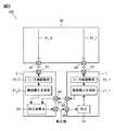
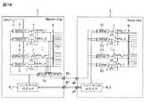
図1は、本発明に係る表示装置100の構成例を表すブロック図である。[Embodiment 1] <Display device for sequentially transmitting grayscale reference voltage among a plurality of display drivers>
FIG. 1 is a block diagram illustrating a configuration example of a
表示装置100は、表示データに基づいて、表示パネル90の複数のソース線91_1に階調信号を出力可能な第1表示ドライバ1と、同じ表示パネル90の他の複数のソース線91_2に階調信号を出力可能な第2表示ドライバ2とを備え、以下のように構成される。 The
第1表示ドライバ1と第2表示ドライバ2は、それぞれ、ソース線駆動部20_1と20_2、階調電圧生成部21_1と21_2、及び制御回路9_1と9_2を含んで構成される。他に表示パネルのゲート線を駆動するための回路や、ホストプロセッサとのインターフェース回路を含んで構成されてもよい。ソース線駆動部20_1と20_2の出力は、複数のソース線駆動出力端子82を介して、表示パネル90のソース線駆動端子92に電気的に接続される。表示パネル90のソース線駆動端子92は、直接またはデマルチプレクサを介すなどして、ソース線91に接続される。第1表示ドライバ1は、ソース線91_1に対して、ソース線駆動部20_1から出力される階調信号を供給し、第2表示ドライバ2は、ソース線91_2に対して、ソース線駆動部20_2から出力される階調信号を供給する。 The
第1表示ドライバ1と第2表示ドライバ2は、特に制限されないが、例えば、公知のCMOS(Complementary Metal-Oxide-Semiconductor field effect transistor)半導体製造技術を用いて、それぞれ、シリコンなどの単一半導体基板上に形成され、表示パネル90のガラス基板上に、フリップチップ実装される。このとき、各端子(82〜87)はパッド電極であり、バンプ(突起電極)により、表示パネル90側の端子92等と、電気的に接続される。 The
ソース線駆動部20_1と20_2は、それぞれ、階調電圧生成部21_1と21_2から供給される、複数の階調電圧に基づいて、ソース線91_1と91_2を駆動する階調信号を出力する。ソース線駆動部20_1と20_2は、複数のソースアンプ3と階調電圧選択部4とラッチ5を含んで構成される。ラッチ5には、表示データがディジタル値で格納されている。表示データは例えば8ビットである。階調電圧選択部4には、階調電圧生成部21_1と21_2から供給される複数の階調電圧が供給されており、ラッチ5から入力される表示データに基づいて、複数の階調電圧から1つの階調を選択し、または2階調選択してその中間値を出力するなどにより、入力された表示データに対応する階調信号を生成する。階調電圧は例えば80階調であり、8ビットの表示データの上位6〜7ビットによってそのうちの隣接する2階調を選択し、下位2ビットによって、その階調間の0、1/4、2/4、3/4、4/4などの中間的な電位の階調信号が出力される。階調電圧は例えば0V〜6Vであり、ラッチ5は低電圧の例えば1.3Vで動作するので、ラッチ5と階調電圧選択回路4との間には、図示が省略されたレベルシフト回路が設けられている。階調電圧選択回路4で生成された階調信号は、例えばボルテージフォロワ増幅回路で構成されるソースアンプ3を介してソース線駆動出力端子82に出力される。 The source line driver units 20_1 and 20_2 output gradation signals for driving the source lines 91_1 and 91_2 based on the plurality of gradation voltages supplied from the gradation voltage generation units 21_1 and 21_2, respectively. The source line driving units 20_1 and 20_2 include a plurality of
階調電圧生成部21_1と21_2は、それぞれ、複数のDA変換器8と複数のボルテージフォロワ増幅器7と抵抗ラダー6とを含んで構成される。複数のDA変換器8はそれぞれ、制御回路9_1または9_2から供給され或いは入力部に設けられた図示されないレジスタに設定される、ディジタルのグレースケール基準電圧設定値を、アナログのグレースケール基準電圧に変換する。各DA変換器8には、参照電圧Vrefが供給されている。DA変換器8の出力であるアナログのグレースケール基準電圧は、ボルテージフォロワ増幅器7を介して抵抗ラダー6の各タップに接続される。抵抗ラダー6の各タップ間をさらに抵抗分圧することにより、複数の階調電圧が生成される。グレースケール基準電圧は、例えば15レベルであり、ガンマ特性を近似するために、複数の階調電圧の折れ線状の特性を規定する。ガンマ特性は、接続される表示パネル90の特性に基づいて規定される、表示データと階調信号レベルの関係を表す曲線状の特性であって、グレースケール基準電圧を設定することによって、折れ線で近似される。 The gradation voltage generation units 21_1 and 21_2 each include a plurality of DA
第1表示ドライバ1は、第2表示ドライバ2に対して、自己の生成した複数のグレースケール基準電圧を順次伝送可能に構成される。例えば、アナログマルチプレクサ10を設け、制御回路9_1により複数のグレースケール基準電圧を順次選択して、出力端子83を介して出力する。 The
第2表示ドライバ2は、順次伝送されたグレースケール基準電圧に基づいて、第1表示ドライバ1で生成されるグレースケール基準電圧と第2表示ドライバ2で生成されるグレースケール基準電圧との差の絶対値を小さくする較正を実行可能に構成される。ここで、「較正」は、第1表示ドライバ1と第2表示ドライバ2のどちらで実行されてもよい。詳細な実施態様は後述するが、第2表示ドライバ2で受信したグレースケール基準電圧と自己が発生したグレースケール基準電圧とを比較して差を求める。その差に基づいて、第1表示ドライバ1に対して較正値を返送して、第1表示ドライバ1側でグレースケール基準電圧を変更させても良いし、その差に基づいて、第2表示ドライバ2が、自身のグレースケール基準電圧を変更してもよい。 The
以上のように、較正を行うことにより、第1表示ドライバ1で生成されるグレースケール基準電圧と第2表示ドライバ2で生成されるグレースケール基準電圧とを一致させることができる。ここで「一致」とは、工業的に通常発生する誤差を許容する範囲での一致を意味する。第1表示ドライバ1と第2表示ドライバ2との間の製造ばらつきや、供給される電源電圧の差により、複数の表示ドライバ間での出力電圧のばらつきが発生する恐れがある場合であっても、グレースケール基準電圧を一致させることによって、そのばらつきを抑えることができる。 As described above, by performing calibration, the grayscale reference voltage generated by the
特許文献1に記載される技術では、1本のアナログ信号である階調基準電圧のみを受け渡して一致させることにより、複数の表示ドライバ(駆動回路部品)の間での出力電圧のばらつきを抑えようとしているのに対して、本発明では、複数のグレースケール基準電圧全てをそれぞれ一致させているので、複数の表示ドライバの間で、ガンマ特性を一致させることができる。即ち、階調信号のどのレベルでも、出力電圧のばらつきを抑えることができる。 In the technique described in
特許文献2に記載される技術では、複数の階調電圧をマスター表示ドライバからスレーブ表示ドライバに供給することにより、当該複数の階調電圧の全てを等しい電圧に揃えることができる。そのため、複数の階調電圧分の、入出力端子と表示パネル上の配線が必要である。これに対して本発明では、順次伝送しているので、1組の入出力端子83と84と1本の表示パネル上の配線があれば足りる。さらに、較正は表示動作を開始する以前に完了させるので、階調電圧を受け渡す信号線に、表示動作中に、ノイズが混入しても、表示には影響しない。 In the technique described in
以上述べたように、表示ドライバのチップ面積の増大や、表示パネルの配線面積の増加を最小限に抑え、且つノイズ耐性を高く保ちながら、複数の表示ドライバ間での出力電圧のばらつきを抑えることを可能とした、表示装置を提供することができる。 As described above, minimizing the increase in the chip area of the display driver and the increase in the wiring area of the display panel, and suppressing the variation in output voltage among multiple display drivers while maintaining high noise resistance. It is possible to provide a display device that makes it possible.
複数の表示ドライバ間でグレースケール基準電圧を一致させる較正の動作は、比較・演算を繰り返しながら誤差を徐々に小さくする収束方式でも、誤差を1回で算出してフィードバックする解析的方式でも良い。また、較正期間中のノイズの影響を軽減するため、複数回の較正動作により、平均値で較正値を求め、或いは、多数決で較正値を求めることもできる。 The calibration operation for matching the gray scale reference voltages among a plurality of display drivers may be a convergence method in which the error is gradually reduced while repeating comparison and calculation, or an analytical method in which the error is calculated and fed back once. Moreover, in order to reduce the influence of noise during the calibration period, the calibration value can be obtained by an average value or the majority value can be obtained by a plurality of calibration operations.
複数の表示ドライバ間でグレースケール基準電圧を一致させる較正は、例えば、表示装置の電源投入時に、パワーアップシーケンスの一環として実施される。これにより、表示装置や表示ドライバに経年変化があった場合にもそれに追随した較正を実施することができる。さらに、表示の帰線期間ごとに較正を実施してもよい。このとき、かならずしも複数のグレースケール基準電圧の全てについて1回の帰線期間内で較正を完了する必要はなく、複数の帰線期間に渡って順次実行すればよい。これにより、表示動作を継続しながらも逐次、較正を実行することができ、温度や電源電圧変動によって出力電圧にばらつきが生じる場合であっても、そのばらつきを抑えることができる。また、較正の結果を保持可能な不揮発性メモリを、表示ドライバ内もしくは外付けに備えることができる。不揮発性メモリには、上記のような較正を行った結果である、DA変換器8への入力データを格納しておき、動作時に読み出して較正されたグレースケール基準電圧を再現させることができる。 Calibration for matching the grayscale reference voltage among the plurality of display drivers is performed as part of a power-up sequence, for example, when the display device is turned on. Thereby, even when there is a secular change in the display device or the display driver, it is possible to carry out calibration following the change. Further, calibration may be performed for each blanking period of the display. At this time, it is not always necessary to complete the calibration within one retrace period for all of the plurality of gray scale reference voltages, and they may be executed sequentially over a plurality of retrace periods. Accordingly, the calibration can be sequentially performed while the display operation is continued, and even when the output voltage varies due to temperature and power supply voltage fluctuations, the variation can be suppressed. In addition, a nonvolatile memory capable of holding the calibration result can be provided in the display driver or externally. The nonvolatile memory can store the input data to the
複数の表示ドライバ間でグレースケール基準電圧を一致させる較正は、例えば、また、表示装置の出荷時に、装置のトリミングとして実行することができる。複数の表示ドライバ間での出力電圧のばらつきが、主に表示ドライバと表示パネルの特性によって発生し、経年変化や、温度依存性、電源電圧依存性が無視できる場合には、出荷時のトリミングのみを行えば十分である。トリミング値は、例えば、不揮発性メモリを、表示ドライバ内もしくは外付けに備えて、それに格納すればよい。 Calibration for matching the gray scale reference voltage among a plurality of display drivers can be performed, for example, as a trimming of the device when the display device is shipped. Output voltage variation among multiple display drivers mainly occurs due to the characteristics of the display driver and the display panel. If aging, temperature dependency, and power supply voltage dependency can be ignored, only trimming at the time of shipment is possible. Is sufficient. The trimming value may be stored in, for example, a nonvolatile memory provided in the display driver or externally.
本発明に係る表示装置100の種々の実装形態について説明する。 Various implementations of the
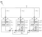
<第2表示ドライバ(マスター)で算出した較正値を第1表示ドライバ(スレーブ)に返送>
図2は、表示装置100の第1の構成例を表す概略ブロック図である。表示装置100は、表示パネル90と、マスターとして機能する第2表示ドライバ2と、スレーブとして機能する第1表示ドライバ1とを含んで構成される。ここで「マスター」とは、同一表示パネルに接続される、複数の表示ドライバが存在するときに、グレースケール基準電圧の較正における基準となる表示ドライバを指し、「スレーブ」とはマスターのグレースケール基準電圧に一致させるように、自己のグレースケール基準電圧を調整する表示ドライバを指す。この用語の定義は、本明細書全体に適用される。<Return the calibration value calculated by the second display driver (master) to the first display driver (slave)>
FIG. 2 is a schematic block diagram illustrating a first configuration example of the
第2表示ドライバ2は、端子82と92を介して表示パネル90のソース線91_2に接続され、第1表示ドライバ1は、端子82と92を介して表示パネル90のソース線91_1に接続されている。 The
第2表示ドライバ2は、ソース線駆動部20_2と、階調電圧生成部21_2と、較正値算出部29と、グレースケール基準電圧入力端子84と、較正値出力端子85とを備え、第1表示ドライバ1は、ソース線駆動部20_1と、階調電圧生成部21_1と、較正部30と、グレースケール基準電圧出力端子83と、較正値入力端子86とを備える。第1表示ドライバ1において、階調電圧生成部21_1には図1に示したマルチプレクサ10が含まれ、階調電圧生成部21_1の内部で発生した複数のグレースケール基準電圧が順次選択されて、グレースケール基準電圧出力端子83から出力される。 The
第2表示ドライバ2は、グレースケール基準電圧入力端子84を介して受信した、順次伝送されたグレースケール基準電圧と自己の生成した複数のグレースケール基準電圧のうちの対応するグレースケール基準電圧とを、較正値算出部29によって比較し、その結果に基づいて較正値を算出して、較正値出力端子85から出力する。第1表示ドライバ1は較正値入力端子86を介して受信した較正値に基づいて、較正部30によって、自己の生成するグレースケール基準電圧を較正する。 The
ここで、「較正値算出部」「較正部」は、制御回路9その他の回路で実現される機能を象徴的に示したものであって、必ずしもそのような特定の回路ブロックが実装される必要はない。これは、図2から図5について同様である。 Here, the “calibration value calculation unit” and the “calibration unit” symbolize functions realized by the
これにより、マスター(第2)表示ドライバ2が較正値を算出し、スレーブ(第1)表示ドライバ1が自己の発生するグレースケール基準電圧をマスター側に一致させる方向に較正する、表示装置100を提供することができる。 In this way, the
<複数のスレーブ表示ドライバ>
図3は、表示装置100の第2の構成例を表す概略ブロック図である。1個のマスター(第2)表示ドライバ2と複数のスレーブを備える構成の一例として、第1表示ドライバ1_1と第3表示ドライバ1_3の2個のスレーブを備える構成例が示される。スレーブの数は任意である。図2との違いは、表示パネル90のソース線91_3に接続される、第3表示ドライバ1_3が追加されている点である。追加された第3表示ドライバ1_3は、第1表示ドライバ1_1と同様に、ソース線駆動部20_3と、階調電圧生成部21_3と、較正部30_3と、グレースケール基準電圧出力端子83_3と、較正値入力端子86_3とを備える。第3表示ドライバ1_3の階調電圧生成部21_3にも図1に示したマルチプレクサ10が含まれ、階調電圧生成部21_3の内部で発生した複数のグレースケール基準電圧が順次選択されて、グレースケール基準電圧出力端子83_3から出力される。第1表示ドライバ1_1と第3表示ドライバ1_3のグレースケール基準電圧出力端子83_1と83_3は、配線で短絡されて、マスター(第2)表示ドライバ2のグレースケール基準電圧出力端子84に接続される。信号の衝突を避けるために、第1表示ドライバ1と第3表示ドライバ3はそれぞれアナログスイッチ22_1と22_3を備える。これに代えて、マスター(第2)表示ドライバ2に個別の入力端子を設けても良い。<Multiple slave display drivers>
FIG. 3 is a schematic block diagram illustrating a second configuration example of the
スレーブ(第1と第3)表示ドライバ1_1と1_3は、マスター(第2)表示ドライバ2に対して、それぞれ順次自己が発生したグレースケール基準電圧をグレースケール基準電圧出力端子83_1と83_3を介して送出する。マスター(第2)表示ドライバ2は順次較正値を算出してスレーブ(第1と第3)表示ドライバ1_1と1_3に返送する。返送されたスレーブ(第1と第3)表示ドライバ1_1と1_3は、返送された較正値に基づいて、自己が発生するグレースケール基準電圧を較正する。 The slave (first and third) display drivers 1_1 and 1_3 send the grayscale reference voltages generated by themselves to the master (second)
これにより、1個のマスター(第2)表示ドライバと複数個のスレーブ(第1、第3等)表示ドライバを備える表示装置において、表示ドライバのチップ面積の増大や、表示パネルの配線面積の増加を最小限に抑え、且つノイズ耐性を高く保ちながら、複数の表示ドライバ間での出力電圧のばらつきを抑えることができる。 Accordingly, in a display device including one master (second) display driver and a plurality of slave (first, third, etc.) display drivers, the chip area of the display driver is increased and the wiring area of the display panel is increased. It is possible to suppress variations in output voltage among a plurality of display drivers while minimizing noise and maintaining high noise resistance.
<第1表示ドライバ(マスター)から伝送されるグレースケール基準電圧を基準に、第2表示ドライバ(スレーブ)が自己較正>
図4は、表示装置の第3の構成例を表す概略ブロック図である。表示装置100は、表示パネル90と、マスターとして機能する第1表示ドライバ1と、スレーブとして機能する第2表示ドライバ2とを含んで構成される。<The second display driver (slave) is self-calibrating based on the grayscale reference voltage transmitted from the first display driver (master)>
FIG. 4 is a schematic block diagram illustrating a third configuration example of the display device. The
第1表示ドライバ1は、端子82と92を介して表示パネル90のソース線91_1に接続され、第2表示ドライバ2は、端子82と92を介して表示パネル90のソース線91_2に接続されている。 The
第1表示ドライバ1は、ソース線駆動部20_1と、階調電圧生成部21_1と、グレースケール基準電圧出力端子83とを備え、第2表示ドライバ2は、ソース線駆動部20_2と、階調電圧生成部21_2と、較正値算出部29と、グレースケール基準電圧入力端子84と、較正部30とを備える。第1表示ドライバ1において、階調電圧生成部21_1には図1に示したマルチプレクサ10が含まれ、階調電圧生成部21_1の内部で発生した複数のグレースケール基準電圧が順次選択されて、グレースケール基準電圧出力端子83から出力される。 The
第2表示ドライバ2は、グレースケール基準電圧入力端子84を介して受信した、順次伝送されたグレースケール基準電圧と自己の生成した前記複数のグレースケール基準電圧のうちの対応するグレースケール基準電圧とを、較正値算出部29によって比較し、その比較の結果に基づいて、較正部30によって、自己の生成するグレースケール基準電圧を較正する。スレーブ(第2)表示ドライバは、マスター(第1)表示ドライバから順次伝送されたグレースケール基準電圧を、自己が生成したグレースケール基準電圧と比較することによって、スレーブ(第2)表示ドライバが自己の発生するグレースケール基準電圧をマスター側に一致させる方向に較正する。 The
これにより、マスター(第1)表示ドライバから伝送されるグレースケール基準電圧を基準に、スレーブ(第2)表示ドライバが、自己の発生するグレースケール基準電圧をマスター側に一致させる方向に自律的に較正する、表示装置を提供することができる。 This allows the slave (second) display driver to autonomously move the gray scale reference voltage generated by the slave (second) display driver to the master side based on the gray scale reference voltage transmitted from the master (first) display driver. A display device can be provided for calibration.
<複数のスレーブ(第2、第4等)表示ドライバが並列に自己較正>
図5は、表示装置の第4の構成例を表す概略ブロック図である。1個のマスター(第1)表示ドライバ1と複数のスレーブを備える構成の一例として、第2表示ドライバ2_2と第4表示ドライバ2_3の2個のスレーブを備える構成例が示される。スレーブの数は任意である。図4との違いは、表示パネル90のソース線91_3に接続される、第4表示ドライバ2_3が追加されている点である。追加された第4表示ドライバ2_3は、第2表示ドライバ2_2と同様に、ソース線駆動部20_3と、階調電圧生成部21_3と、較正値算出部29と、グレースケール基準電圧入力端子84_3と、較正部30_3とを備える。<Self-calibration of multiple slave (second, fourth, etc.) display drivers in parallel>
FIG. 5 is a schematic block diagram illustrating a fourth configuration example of the display device. As an example of a configuration including one master (first)
マスターである第1表示ドライバ1は、第2表示ドライバ2_2と第4表示ドライバ2_3に対して並行して、自己の生成した複数のグレースケール基準電圧を、グレースケール基準電圧出力端子83を介して順次送出する。第2表示ドライバ2_2は、グレースケール基準電圧入力端子84_2を介して受信した、順次伝送されたグレースケール基準電圧と自己の生成した前記複数のグレースケール基準電圧のうちの対応するグレースケール基準電圧とを、較正値算出部29_2によって比較し、その比較の結果に基づいて、較正部30_2によって、自己の生成するグレースケール基準電圧を較正する。これと並行に、第4表示ドライバ2_4も、グレースケール基準電圧入力端子84_3を介して受信した、順次伝送されたグレースケール基準電圧と自己の生成した前記複数のグレースケール基準電圧のうちの対応するグレースケール基準電圧とを、較正値算出部29_3によって比較し、その比較の結果に基づいて、較正部30_3によって、自己の生成するグレースケール基準電圧を較正する。マスター(第1)表示ドライバ1は、複数個のスレーブ(第2、第4等)表示ドライバ2_2と2_3に対して並行に、自己が発生した複数のグレースケール基準電圧を順次送出し、複数個のスレーブ(第2、第4等)表示ドライバ2_2と2_3は、それぞれ、自己が発生するグレースケール基準電圧を受信した、マスターのグレースケール基準電圧に一致させる方向に較正する。 The
これにより、1個のマスター(第1)表示ドライバと複数個のスレーブ(第2、第4等)表示ドライバを備える表示装置において、表示ドライバのチップ面積の増大や、表示パネルの配線面積の増加を最小限に抑え、且つノイズ耐性を高く保ちながら、複数の表示ドライバ間での出力電圧のばらつきを抑えることができる。 Accordingly, in a display device including one master (first) display driver and a plurality of slave (second, fourth, etc.) display drivers, the chip area of the display driver and the wiring area of the display panel are increased. It is possible to suppress variations in output voltage among a plurality of display drivers while minimizing noise and maintaining high noise resistance.
<まとめ>
マスターとスレーブの表示ドライバは、別品種の表示ドライバICとして実現しても良いし、マスターモードとスレーブモードの2つの動作モードを持つ1つの品種として実現しても良い。<Summary>
The master and slave display drivers may be realized as different types of display driver ICs, or may be realized as one type having two operation modes of the master mode and the slave mode.
別品種として実現される場合、上記図3に示される実施態様では、比較的回路規模が大きい、較正値算出部をマスター表示ドライバにのみ設ければ済むのに対して、図5に示される実施態様では、較正値算出部を各スレーブ表示ドライバに設ける必要があるため、図3に示される実施態様の方が、チップコストは低い。また、図5に示される実施態様では、各スレーブ表示ドライバに設けられた較正値算出部の相互ばらつきの影響を受けるが、図3に示される実施態様ではその問題がない。これは、マスターとスレーブの表示ドライバを、別品種の表示ドライバICとして実現した場合も、マスターモードとスレーブモードの2つの動作モードを持つ1つの品種として実現した場合も同様である。 When implemented as a different product, the embodiment shown in FIG. 3 has a relatively large circuit scale, and the calibration value calculation unit need only be provided in the master display driver, whereas the implementation shown in FIG. In the aspect, since it is necessary to provide a calibration value calculation unit in each slave display driver, the embodiment shown in FIG. 3 has a lower chip cost. Further, the embodiment shown in FIG. 5 is affected by the mutual variation of the calibration value calculation units provided in each slave display driver, but there is no such problem in the embodiment shown in FIG. This is the same when the master and slave display drivers are realized as different types of display driver ICs or when they are realized as one type having two operation modes of the master mode and the slave mode.
図3に示される実施態様では、複数のスレーブに対する較正を、順次または時分割で実行する必要があるのに対し、図5に示される実施態様では、複数のスレーブに対して並行に較正を実行することができるので、より短時間で較正を実行することができる。 In the embodiment shown in FIG. 3, calibration for multiple slaves needs to be performed sequentially or in time division, whereas in the embodiment shown in FIG. 5, calibration is performed on multiple slaves in parallel. Calibration can be performed in a shorter time.
グレースケール基準電圧は、表示ドライバ間でアナログ信号として伝送されるが、較正を行うための比較は、アナログで行っても、ディジタルで行っても良い。以下に詳述する、実施形態2〜実施形態4は、そのうちの中の代表的な実施形態である。実施形態2と3はディジタル値で比較して較正を行う例であり、実施形態4と5はアナログ電圧で比較して較正を行う例である。 The gray scale reference voltage is transmitted as an analog signal between the display drivers, but the comparison for performing the calibration may be performed by analog or digital.
〔実施形態2〕<マスターにADCを搭載してディジタル値で比較>
図6は、本発明の実施形態2に係る表示ドライバの構成例を表すブロック図である。[Embodiment 2] <Comparison with digital values by installing ADC in master>
FIG. 6 is a block diagram illustrating a configuration example of a display driver according to the second embodiment of the present invention.
図2を引用して説明した、スレーブ表示ドライバ1からマスター表示ドライバ2にグレースケール基準電圧を順次伝送し、マスター側で、自己が生成したグレースケール基準電圧と受信したグレースケール基準電圧の比較を行うことによって較正値を算出し、算出した較正値をマスター表示ドライバ2からスレーブ表示ドライバ1に返送する構成である。図6には、マスター表示ドライバ2とスレーブ表示ドライバ1のみが示され、表示パネル90は図示を省略されている。また、表示ドライバ1と2の内部は、ソース線駆動部20_1と20_2等は省略され、階調電圧生成部21_1と21_2と、制御回路(コントロールロジック)9_1と9_2を含む較正値算出部29の具体的な構成例が、詳しく示される。この構成は、図3に示される、1個のマスター表示ドライバと複数個のスレーブ表示ドライバを備える表示装置100にも、同様に適用され得る。 The gray scale reference voltage is sequentially transmitted from the
スレーブ表示ドライバ1とマスター表示ドライバ2において、複数のDA変換器8と複数のボルテージフォロワ増幅器7と抵抗ラダー6は、それぞれ、階調電圧生成部21_1と21_2を構成している。複数のボルテージフォロワ増幅器7からは、それぞれのタップのグレースケール基準電圧が出力され、抵抗ラダー6に供給されている。 In the
スレーブ表示ドライバ1において、各タップのグレースケール基準電圧は、マルチプレクサ10に入力され、コントロールロジック9_1によって選択される1個のグレースケール基準電圧が、グレースケール基準電圧出力端子83から出力される。 In the
マスター表示ドライバ2において、較正値算出部29は、マルチプレクサ11とマルチプレクサ12とAD変換器13とメモリ17と比較・演算部18とコントロールロジック9_2を含んで構成される。マルチプレクサ11と12はそれぞれ、入力された複数の信号から1つの信号を選択して、選択された信号のアナログ電圧を出力する、アナログマルチプレクサである。AD変換器13は、アナログ電圧をディジタル値に変換する回路で、特に制限されないが例えば、逐次比較型、シグマデルタ型等の方式が採用される。メモリ17は、特に制限されないが例えば、SRAM(Static Random Access Memory)やレジスタによって構成される。比較・演算部18はメモリ17にアクセス可能に構成され、メモリ17から読み出したデータ間の演算を行い、結果をメモリ17に書き込むことができる。コントロールロジック9_2がMPU(Micro Processing Unit)などのプロセッサで構成されるときに、その機能の一部として実装されてもよい。 In the
表示ドライバ1と2の動作について説明する。 The operation of the
スレーブ表示ドライバ1において、各タップのグレースケール基準電圧は、マルチプレクサ10によって順次選択されて、グレースケール基準電圧出力端子83から出力される。 In the
マスター表示ドライバ2において、各タップのグレースケール基準電圧は、マルチプレクサ11に入力され、コントロールロジック9_2によって選択される1個のグレースケール基準電圧が、マルチプレクサ12の一方の入力端子に入力される。マルチプレクサ12の他方の入力端子には、グレースケール基準電圧入力端子84から入力された、スレーブ表示ドライバ1のグレースケール基準電圧が入力される。コントロールロジック9_2によって選択される一方のグレースケール基準電圧が、マルチプレクサ12からAD変換器13に入力される。AD変換器13の出力はメモリ17に格納される。比較・演算部18は、ディジタル化されたグレースケール基準電圧を読み出して、比較、演算等を行うことにより、較正値を算出する。 In the
スレーブ表示ドライバ1内で生成された複数のグレースケール基準電圧は、マルチプレクサ11で順次選択され、マルチプレクサ12を経由してAD変換器13に入力され、ディジタル値に変換されて、変換結果であるディジタル値がメモリ17に格納される。グレースケール基準電圧入力端子84から入力された、スレーブ表示ドライバ1の複数のグレースケール基準電圧も、順次、マルチプレクサ12を経由してAD変換器13に入力され、ディジタル値に変換されて、変換結果であるディジタル値がメモリ17に格納される。比較・演算部18は、互いに対応するタップどうしの、スレーブ表示ドライバ1のグレースケール基準電圧とマスター表示ドライバ2のグレースケール基準電圧とを読出して比較し、スレーブ表示ドライバ1のグレースケール基準電圧の較正値を算出する。算出された較正値は、コントロールロジック9_2から較正値出力端子85を通してマスター表示ドライバ1に送出される。較正値を受信したマスター表示ドライバ1は、較正値を各タップのDA変換器8に供給することにより、グレースケール基準電圧を較正する。 A plurality of gray scale reference voltages generated in the
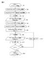
図7は、本発明の実施形態2に係る表示ドライバの動作例を表すフローチャートである。 FIG. 7 is a flowchart showing an operation example of the display driver according to the second embodiment of the present invention.
スレーブ表示ドライバ1の第nタップのグレースケール基準電圧を較正する場合の動作例である。 It is an operation example in the case of calibrating the gray scale reference voltage of the nth tap of the
マスター表示ドライバ2において、マルチプレクサ11によって第nタップTAPm_nを選択し(S2)、マルチプレクサ12によってマスター側を選択し(S3)、マスター側の第nタップのグレースケール基準電圧をAD変換器13に入力してディジタル値に変換し(S4)、その変換結果(MS)をメモリ17に格納する(S5)。 In the
次に、スレーブ表示ドライバ1において、マルチプレクサ10によって第nタップTAPs_nを選択して(S6)、第nタップのグレースケール基準電圧をグレースケール基準電圧出力端子83から出力する。マスター表示ドライバ2では、マルチプレクサ12によってスレーブ側を選択する(S7)。スレーブ表示ドライバ1において、第nタップのグレースケール基準電圧のための、DA変換器8の入力データDsnにゼロ(0)を設定する(S8)。マスター表示ドライバ2では、グレースケール基準電圧入力端子84から入力された、スレーブ側の第nタップのグレースケール基準電圧をAD変換器13に入力してディジタル値に変換し(S9)、その変換結果(SL)をメモリ17に格納する(S10)。メモリ17からマスター側のデータMSとスレーブ側のデータSLとを読み出して、比較・演算部18によって、その差D=MS−SLを算出する(S11)。DA変換器8の入力データDsnを算出した差によって補正(Dsn=Dsn+D)する(S13)。差Dの絶対値が所定の誤差未満になるまで、ステップS9からS13を繰り返す(S12)。図7のS12においてD=0と表記されるのは、差Dの絶対値が所定の誤差未満か否かの判断を示すものである。差Dの絶対値が所定の誤差未満になれば、第nタップTAPs_nの較正を終了する(S20)。差D=0になれば、マスターとスレーブの第nタップのグレースケール基準電圧は一致する。工業的に許容される範囲内の誤差以内に入れば、一致したものとして較正を終了してよい。 Next, in the
上記の各ステップを全てのタップについて繰り返すことにより、スレーブ表示ドライバ1の全てのタップにおいて、グレースケール基準電圧を、マスター表示ドライバ2の対応するタップのグレースケール基準電圧に、一致させることができる。 By repeating the above steps for all the taps, the grayscale reference voltage can be matched with the grayscale reference voltage of the corresponding tap of the
図8は、本発明の実施形態2に係る表示ドライバの別の動作例を表すフローチャートである。 FIG. 8 is a flowchart showing another operation example of the display driver according to the second embodiment of the present invention.
図7と同様に、スレーブ表示ドライバ1の第nタップのグレースケール基準電圧を較正する場合の動作例であり、ステップS1からS10は上述と同様である。図7に示した動作例では、ステップS11において、マスター側のデータMSとスレーブ側のデータSLの差D=MS−SLを算出するのに対して、MSとSLが一致しているか否かを判定し(S14)、不一致の場合にはスレーブ側のDA変換器8の入力データDsnを1だけ増やす(S15)。ステップS9、S10,S14,S15をマスター側のデータMSとスレーブ側のデータSLが一致するまで繰り返し、一致したら終了する(S20)。 As in FIG. 7, this is an operation example when the gray scale reference voltage of the nth tap of the
上記の各ステップを全てのタップについて繰り返すことにより、スレーブ表示ドライバ1の全てのタップにおいて、グレースケール基準電圧を、マスター表示ドライバ2の対応するタップのグレースケール基準電圧に、一致させることができる。 By repeating the above steps for all the taps, the grayscale reference voltage can be matched with the grayscale reference voltage of the corresponding tap of the
〔実施形態3〕<スレーブにADCを搭載してディジタル値で比較>
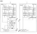
図9は、本発明の実施形態3に係る表示ドライバの構成例を表すブロック図である。[Embodiment 3] <Comparison with digital values by installing ADC in slave>
FIG. 9 is a block diagram illustrating a configuration example of a display driver according to the third embodiment of the present invention.
図4を引用して説明した、マスター表示ドライバ1からスレーブ表示ドライバ2に較正の基準となるグレースケール基準電圧を順次伝送し、スレーブ側で、自己が生成したグレースケール基準電圧と受信したグレースケール基準電圧の比較を行うことによって、スレーブ表示ドライバ2で生成するグレースケール基準電圧を較正する構成である。図9には、マスター表示ドライバ1とスレーブ表示ドライバ2のみが示され、表示パネル90は図示を省略されている。また、表示ドライバ1と2の内部は、ソース線駆動部20_1と20_2等は省略され、階調電圧生成部21_1と21_2と、制御回路(コントロールロジック)9_1と9_2を含む較正値算出部29と較正部30の具体的な構成例が、詳しく示される。この構成は、図5に示される、1個のマスター表示ドライバと複数個のスレーブ表示ドライバを備える表示装置100にも、同様に適用され得る。 The gray scale reference voltage, which is a calibration reference, is sequentially transmitted from the
マスター表示ドライバ1とスレーブ表示ドライバ2において、複数のDA変換器8と複数のボルテージフォロワ増幅器7と抵抗ラダー6は、それぞれ、階調電圧生成部21_1と21_2を構成している。複数のボルテージフォロワ増幅器7からは、それぞれのタップのグレースケール基準電圧が出力され、抵抗ラダー6に供給されている。 In the
マスター表示ドライバ1において、各タップのグレースケール基準電圧は、マルチプレクサ10に入力され、コントロールロジック9_1によって選択される1個のグレースケール基準電圧が、グレースケール基準電圧出力端子83から出力される。 In the
スレーブ表示ドライバ2において、較正値算出部29と較正部30は、マルチプレクサ11とマルチプレクサ12とAD変換器13とメモリ17と比較・演算部18とコントロールロジック9_2を含んで構成される。各タップのグレースケール基準電圧は、マルチプレクサ11に入力され、コントロールロジック9_2によって選択される1個のグレースケール基準電圧が、マルチプレクサ12の一方の入力端子に入力される。マルチプレクサ12の他方の入力端子には、グレースケール基準電圧入力端子84から入力された、マスター表示ドライバ1のグレースケール基準電圧が入力される。コントロールロジック9_2によって選択される一方のグレースケール基準電圧が、マルチプレクサ12からAD変換器13に入力される。AD変換器13の出力はメモリ17に格納される。比較・演算部18は、ディジタル化されたグレースケール基準電圧を読み出して、比較、演算等を行うことにより、較正値を算出する。 In the
コントロールロジック9_1とコントロールロジック9_2は、制御情報入出力端子87を介して互いに通信することができるように、接続されている。実施形態2とは異なり、較正値を送受する必要はないので、この通信路は、表示の同期のために使用される。 The control logic 9_1 and the control logic 9_2 are connected so that they can communicate with each other via the control information input /
表示ドライバ1と2の動作について説明する。 The operation of the
スレーブ表示ドライバ2内で生成された複数のグレースケール基準電圧は、マルチプレクサ11で順次選択され、マルチプレクサ12を経由してAD変換器13に入力され、ディジタル値に変換されて、変換結果であるディジタル値がメモリ17に格納される。グレースケール基準電圧入力端子84から入力された、マスター表示ドライバ1の複数のグレースケール基準電圧も、順次、マルチプレクサ12を経由してAD変換器13に入力され、ディジタル値に変換されて、変換結果であるディジタル値がメモリ17に格納される。比較・演算部18は、互いに対応するタップどうしの、マスター表示ドライバ1のグレースケール基準電圧とスレーブ表示ドライバ2のグレースケール基準電圧とを読出して比較し、スレーブ表示ドライバ2のグレースケール基準電圧の較正値を算出する。スレーブ表示ドライバ2は、算出された較正値を、コントロールロジック9_2を介して階調電圧生成部21_2の対応するタップのDA変換器8に入力することにより、当該タップのグレースケール基準電圧を較正する。 The plurality of gray scale reference voltages generated in the
本実施形態3に係る表示ドライバの動作は、図7と図8を引用して説明した、実施形態2に係る表示ドライバの動作と同様である。実施形態2では、マスター表示ドライバ2が図7と図8のフローチャートに示される動作を実行するのに対して、本実施形態3に係る表示ドライバでは、スレーブ表示ドライバ2が図7と図8のフローチャートに示される動作を実行する。 The operation of the display driver according to the third embodiment is the same as the operation of the display driver according to the second embodiment described with reference to FIGS. In the second embodiment, the
〔実施形態4〕<マスターにコンパレータを搭載してアナログ電圧で比較>
図10は、本発明の実施形態4に係る表示ドライバの構成例を表すブロック図である。[Embodiment 4] <Comparison with analog voltage with a comparator mounted on the master>
FIG. 10 is a block diagram illustrating a configuration example of a display driver according to the fourth embodiment of the present invention.
実施形態2(図6)と同様に、図2を引用して説明した、スレーブ表示ドライバ1からマスター表示ドライバ2にグレースケール基準電圧を順次伝送し、マスター側で、自己が生成したグレースケール基準電圧と受信したグレースケール基準電圧の比較を行うことによって較正値を算出し、算出した較正値をマスター表示ドライバ2からスレーブ表示ドライバ1に返送する構成である。実施形態2(図6)がグレースケール基準電圧をディジタル化して比較し、較正値を求めたのに対し、本実施形態では、アナログ電圧のまま比較を行う。図10には、マスター表示ドライバ2とスレーブ表示ドライバ1のみが示され、表示パネル90は図示を省略されている。また、表示ドライバ1と2の内部は、ソース線駆動部20_1と20_2等は省略され、階調電圧生成部21_1と21_2と、制御回路(コントロールロジック)9_1と9_2を含む較正値算出部29の具体的な構成例が、詳しく示される。この構成は、図3に示される、1個のマスター表示ドライバと複数個のスレーブ表示ドライバを備える表示装置100にも、同様に適用され得る。 As in the second embodiment (FIG. 6), the grayscale reference voltage is sequentially transmitted from the
スレーブ表示ドライバ1とマスター表示ドライバ2において、複数のDA変換器8と複数のボルテージフォロワ増幅器7と抵抗ラダー6は、それぞれ、階調電圧生成部21_1と21_2を構成している。複数のボルテージフォロワ増幅器7からは、それぞれのタップのグレースケール基準電圧が出力され、抵抗ラダー6に供給されている。 In the
スレーブ表示ドライバ1において、各タップのグレースケール基準電圧は、マルチプレクサ10に入力され、コントロールロジック9_1によって選択される1個のグレースケール基準電圧が、グレースケール基準電圧出力端子83から出力される。 In the
マスター表示ドライバ2において、較正値算出部29は、マルチプレクサ11とクロスバースイッチ付きコンパレータ14とメモリ17と演算部19とコントロールロジック9_2を含んで構成される。マルチプレクサ11には、各タップのグレースケール基準電圧が入力され、コントロールロジック9_2によって指定されるタップのグレースケール基準電圧をクロスバースイッチ付きコンパレータ14の一方の入力に供給する。クロスバースイッチ付きコンパレータ14の他方の入力には、グレースケール基準電圧入力端子84で受信した、スレーブ表示ドライバ1の各タップのグレースケール基準電圧が入力される。コンパレータ14の出力はメモリ17に格納される。演算部19は、メモリ17にアクセス可能に構成され、メモリ17から読み出したデータ間の演算を行い、結果をメモリ17に書き込むことができ、コントロールロジック9_2がMPUなどのプロセッサで構成されるときに、その機能の一部として実装されてもよい。 In the
図11は、クロスバースイッチ付きコンパレータ14の動作を説明するための回路図である。図11に示されるように、クロスバースイッチ15は、コンパレータ16の入力を入れ替えることができるように構成される、(a)に示されるフェーズAでは、VIN1がVPに入力され、VIN2がVMに入力される。(b)に示されるフェーズBでは、逆に、VIN1はVMに入力され、VIN2はVPに入力される。クロスバースイッチ15によって入力を入れ替えることにより、コンパレータ16の入力オフセットを相殺することができる。例えば、まずフェーズAにおいて、VIN1を固定してVIN2を徐々に増加し、コンパレータ16の出力が反転する箇所を求める。次にフェーズBにおいても同様に、VIN1を固定してVIN2を徐々に増加し、コンパレータ16の出力が反転する箇所を求める。コンパレータ16に入力オフセットが無ければ、反転箇所はフェーズAとフェーズBで一致するが、入力オフセットがあれば不一致となる。フェーズAとフェーズBにおける反転箇所の中間値から、入力オフセットがない場合の反転箇所を推定することができる。この方法により、クロスバースイッチ付きコンパレータ14を用いて、コンパレータ16の入力オフセットを相殺することができる。 FIG. 11 is a circuit diagram for explaining the operation of the
図12は、本発明の実施形態4に係る表示ドライバの動作例を表すフローチャートである。 FIG. 12 is a flowchart showing an operation example of the display driver according to the fourth embodiment of the present invention.
スレーブ表示ドライバ1の第nタップのグレースケール基準電圧を較正する場合の動作例である。 It is an operation example in the case of calibrating the gray scale reference voltage of the nth tap of the
マスター表示ドライバ2においてマルチプレクサ11によって第nタップTAPm_nを選択し、スレーブ表示ドライバ1においてマルチプレクサ10によって第nタップTAPs_nを選択し、クロスバースイッチ付きコンパレータ14のVIN1にマスター表示ドライバ2のマルチプレクサ11の出力を、VIN2にスレーブ表示ドライバ1のマルチプレクサ10の出力を、それぞれ供給する(S21)。クロスバースイッチ15をフェーズAに設定する(S22)。 In the
パラメータiを使ったループを開始する。まずi=0に初期化する(S23)。スレーブ表示ドライバ1の第nタップのDA変換器8の入力データDsnとして、パラメータiを入力する(S24)。第nタップのDA変換器8の入力データDsnをデータSLAとしてメモリ17に格納しておく(S25)。コンパレータ14による比較を行い(S26)、コンパレータ出力CMPを、i番目のコンパレータ出力D_CMP(i)として、メモリに格納する(S27)。ループにおける1回前の、i−1番目のコンパレータ出力D_CMP(i−1)と、i番目のコンパレータ出力D_CMP(i)とを比較し(S28)、一致していれば、パラメータiを増や(+1)して(S29)、ステップS24に戻る。パラメータiを1ずつ増やしながら、i−1番目のコンパレータ出力D_CMP(i−1)とi番目のコンパレータ出力D_CMP(i)とが一致するまで繰り返し、一致した時点でループを抜ける。ループを抜けた時点で、フェーズAでコンパレータ出力D_CMPが反転する箇所のDA変換器8の入力データDsnが、SLAとしてメモリ17に保持されている。 Start loop using parameter i. First, i = 0 is initialized (S23). The parameter i is input as the input data Dsn of the
次に、クロスバースイッチ15をフェーズBに設定し(S30)、パラメータjを使った同様のループを開始する。まずj=0に初期化する(S31)。スレーブ表示ドライバ1の第nタップのDA変換器8の入力データDsnとして、パラメータjを入力する(S32)。第nタップのDA変換器8の入力データDsnをデータSLBとしてメモリ17に格納しておく(S33)。コンパレータ14による比較を行い(S34)、コンパレータ出力CMPを、j番目のコンパレータ出力D_CMP(j)として、メモリに格納する(S35)。ループにおける1回前の、j−1番目のコンパレータ出力D_CMP(j−1)と、j番目のコンパレータ出力D_CMP(j)とを比較し(S36)、一致していれば、パラメータjを増や(+1)して(S37)、ステップS32に戻る。パラメータjを1ずつ増やしながら、j−1番目のコンパレータ出力D_CMP(j−1)とj番目のコンパレータ出力D_CMP(j)とが一致するまで繰り返し、一致した時点でループを抜ける。ループを抜けた時点で、フェーズBでコンパレータ出力D_CMPが反転する箇所のDA変換器8の入力データDsnが、SLBとしてメモリ17に保持されている。 Next, the
SLAとSLBの平均値をDA変換器8の入力データDsnの較正値として算出し(S38)、第nタップTAPs_nの較正を終了する(S40)。 The average value of SLA and SLB is calculated as the calibration value of the input data Dsn of the DA converter 8 (S38), and the calibration of the nth tap TAPs_n is completed (S40).
上記の各ステップを全てのタップについて繰り返すことにより、スレーブ表示ドライバ1の全てのタップにおいて、グレースケール基準電圧を、マスター表示ドライバ2の対応するタップのグレースケール基準電圧に、一致させることができる。 By repeating the above steps for all the taps, the grayscale reference voltage can be matched with the grayscale reference voltage of the corresponding tap of the
〔実施形態5〕<スレーブにコンパレータを搭載してアナログ電圧で比較>
図13は、本発明の実施形態5に係る表示ドライバの構成例を表すブロック図である。[Embodiment 5] <Comparison with analog voltage by mounting a comparator in the slave>
FIG. 13 is a block diagram illustrating a configuration example of a display driver according to the fifth embodiment of the present invention.
実施形態3(図9)と同様に、図4を引用して説明した、マスター表示ドライバ1からスレーブ表示ドライバ2に較正の基準となるグレースケール基準電圧を順次伝送し、スレーブ側で、自己が生成したグレースケール基準電圧と受信したグレースケール基準電圧の比較を行うことによって、スレーブ表示ドライバ2で生成するグレースケール基準電圧を較正する構成である。実施形態3(図9)がグレースケール基準電圧をディジタル化して比較し、較正値を求めたのに対し、本実施形態では、アナログ電圧のまま比較を行う。図13には、マスター表示ドライバ1とスレーブ表示ドライバ2のみが示され、表示パネル90は図示を省略されている。また、表示ドライバ1と2の内部は、ソース線駆動部20_1と20_2等は省略され、階調電圧生成部21_1と21_2と、制御回路(コントロールロジック)9_1と9_2を含む較正値算出部29と較正部30の具体的な構成例が、詳しく示される。この構成は、図5に示される、1個のマスター表示ドライバと複数個のスレーブ表示ドライバを備える表示装置100にも、同様に適用され得る。 Similarly to the third embodiment (FIG. 9), the gray scale reference voltage serving as a calibration reference is sequentially transmitted from the
マスター表示ドライバ1とスレーブ表示ドライバ2において、複数のDA変換器8と複数のボルテージフォロワ増幅器7と抵抗ラダー6は、それぞれ、階調電圧生成部21_1と21_2を構成している。複数のボルテージフォロワ増幅器7からは、それぞれのタップのグレースケール基準電圧が出力され、抵抗ラダー6に供給されている。 In the
マスター表示ドライバ1において、各タップのグレースケール基準電圧は、マルチプレクサ10に入力され、コントロールロジック9_1によって選択される1個のグレースケール基準電圧が、グレースケール基準電圧出力端子83から出力される。 In the
スレーブ表示ドライバ2において、較正値算出部29と較正部30は、マルチプレクサ11とクロスバースイッチ付きコンパレータ14とメモリ17と演算部19とコントロールロジック9_2を含んで構成される。マルチプレクサ11には、各タップのグレースケール基準電圧が入力され、コントロールロジック9_2によって指定されるタップのグレースケール基準電圧をクロスバースイッチ付きコンパレータ14の一方の入力に供給する。クロスバースイッチ付きコンパレータ14の他方の入力には、グレースケール基準電圧入力端子84で受信した、マスター表示ドライバ1の各タップのグレースケール基準電圧が入力される。コンパレータ14の出力はメモリ17に格納される。演算部19は、メモリ17にアクセス可能に構成され、メモリ17から読み出したデータ間の演算を行い、結果をメモリ17に書き込むことができ、コントロールロジック9_2がMPUなどのプロセッサで構成されるときに、その機能の一部として実装されてもよい。 In the
コントロールロジック9_1とコントロールロジック9_2は、制御情報入出力端子87を介して互いに通信することができるように、接続されている。実施形態2とは異なり、較正値を送受する必要はないので、この通信路は、表示の同期のために使用される。 The control logic 9_1 and the control logic 9_2 are connected so that they can communicate with each other via the control information input /
本実施形態5に係る表示ドライバの動作は、図12を引用して説明した、実施形態4に係る表示ドライバの動作と同様である。実施形態4では、マスター表示ドライバ2が図12のフローチャートに示される動作を実行するのに対して、本実施形態5に係る表示ドライバでは、スレーブ表示ドライバ2が図12のフローチャートに示される動作を実行する。 The operation of the display driver according to the fifth embodiment is the same as the operation of the display driver according to the fourth embodiment described with reference to FIG. In the fourth embodiment, the
〔実施形態6〕<スレーブにS/H回路を搭載してマスターの基準電圧をホールド>
実施形態2から5で説明した表示ドライバは、マスターとスレーブの両方の表示ドライバそれぞれに複数のDA変換器8を設けて、その入力データにグレースケール基準電圧に対応するディジタル値を設定することにより、所望のガンマ特性を近似する構成である。マスター側またはスレーブ側の一方から他方へ、複数のグレースケール基準電圧を順次伝送することにより、受信した側で較正値を算出しまたは実際に較正を行うことにより、スレーブ側のグレースケール基準電圧をマスター側に一致させる較正動作を行っている。[Embodiment 6] <S / H circuit mounted on slave to hold master reference voltage>
In the display drivers described in the second to fifth embodiments, a plurality of DA
グレースケール基準電圧は、必ずしもディジタル値で保持される必要はない。本実施形態6では、スレーブ側表示ドライバ2の階調電圧生成部21_2に、複数のDA変換器8に代えて、複数のサンプル・ホールド(S/H:Sample and Hold)回路23が設けられている。 The gray scale reference voltage does not necessarily have to be held as a digital value. In the sixth embodiment, the gradation voltage generation unit 21_2 of the
図14は、本発明の実施形態6に係る表示ドライバの構成例を表すブロック図である。図10には、マスター表示ドライバ1とスレーブ表示ドライバ2のみが示され、表示パネル90は図示を省略されている。また、表示ドライバ1と2の内部は、ソース線駆動部20_1と20_2等は省略され、階調電圧生成部21_1と21_2と制御回路(コントロールロジック)9_1と9_2とを含む具体的な構成例が、詳しく示される。 FIG. 14 is a block diagram illustrating a configuration example of a display driver according to the sixth embodiment of the present invention. FIG. 10 shows only the
マスター表示ドライバ1においては、複数のDA変換器8と複数のボルテージフォロワ増幅器7と抵抗ラダー6が、階調電圧生成部21_1を構成している。複数のボルテージフォロワ増幅器7からは、それぞれのタップのグレースケール基準電圧が出力され、抵抗ラダー6に供給されている。マスター表示ドライバ1において、各タップのグレースケール基準電圧は、マルチプレクサ10に入力され、コントロールロジック9_1によって選択される1個のグレースケール基準電圧が、グレースケール基準電圧出力端子83から出力される。 In the
スレーブ表示ドライバ2においては、複数のサンプル・ホールド(S/H)回路23と複数のボルテージフォロワ増幅器7と抵抗ラダー6が、階調電圧生成部21_2を構成している。グレースケール基準電圧入力端子84から入力される、マスター側のグレースケール基準電圧が、コントロールロジック9_2による制御によって順次、対応するサンプル・ホールド(S/H)回路23にサンプルされ、ホールドされる。 In the
コントロールロジック9_1とコントロールロジック9_2は、制御情報入出力端子87を介して互いに通信することができるように、接続されている。較正値を送受する必要はないので、この通信路は、グレースケール基準電圧の転送の同期のために使用される。表示動作の同期のためにも使用することができる。 The control logic 9_1 and the control logic 9_2 are connected so that they can communicate with each other via the control information input /
図15は、本発明の実施形態6に係る表示ドライバの動作例を表すフローチャートである。 FIG. 15 is a flowchart showing an operation example of the display driver according to the sixth embodiment of the present invention.
スレーブ表示ドライバ2の第nタップのグレースケール基準電圧を、マスター表示ドライバ1の同じ第nタップのグレースケール基準電圧と一致させる場合の動作例である。 This is an operation example when the gray scale reference voltage of the nth tap of the
まず、マスター表示ドライバ1において、マルチプレクサ10により第nタップを選択する(S52)。次にスレーブ表示ドライバ2において、対応する第nサンプル・ホールド回路S/Nsnをサンプル状態にし(S53)、その後ホールド状態に遷移させる(S54)。以上で第nタップのグレースケール基準電圧のサンプル・ホールド動作は完了する(S60)。 First, in the
上記の各ステップを全てのタップについて繰り返すことにより、スレーブ表示ドライバ2の全てのタップのサンプル・ホールド回路において、マスター表示ドライバ2の対応するタップのグレースケール基準電圧をアナログ的に保持することができる。 By repeating the above steps for all the taps, the gray scale reference voltage of the corresponding tap of the
これにより、簡単な回路を設けるだけで、マスター表示ドライバで生成されたグレースケール基準電圧を、スレーブ表示ドライバに複写して、マスター側と等しいグレースケール基準電圧を発生させるように制御することができる、スレーブ表示ドライバを提供することができる。 Thus, it is possible to control the gray scale reference voltage generated by the master display driver to be copied to the slave display driver and generate the same gray scale reference voltage as that of the master side only by providing a simple circuit. A slave display driver can be provided.
このサンプル・ホールド動作は、表示装置100への電源がオンされ、表示ドライバ1と2が起動された後、表示動作を開始する前の期間に実行され、その後は、垂直帰線(V−blank)期間やライン周期の合間に、繰り返し実行される。サンプル・ホールド回路には電荷のリークがあるので、これをリフレッシュする必要があるためである。 This sample and hold operation is executed in a period before the display operation is started after the power to the
以上本発明者によってなされた発明を実施形態に基づいて具体的に説明したが、本発明はそれに限定されるものではなく、その要旨を逸脱しない範囲において種々変更可能であることは言うまでもない。 Although the invention made by the present inventor has been specifically described based on the embodiments, it is needless to say that the present invention is not limited thereto and can be variously modified without departing from the gist thereof.
例えば、本明細書では主に液晶表示パネルを有する表示装置について例を挙げて説明したが、本発明は、画素毎に階調電圧を持った信号で駆動されるアクティブマトリクス型の表示装置に広く適用することができ、例えば、有機EL(organic electroluminescence display: OELD)表示装置、プラズマディスプレイなどに適用することができる。 For example, in this specification, a display device having a liquid crystal display panel is mainly described as an example. However, the present invention is widely applied to an active matrix display device driven by a signal having a gradation voltage for each pixel. For example, it can be applied to an organic EL (organic electroluminescence display: OELD) display device, a plasma display, and the like.
1、2 表示ドライバ
3 ソースアンプ
4 階調電圧選択部
5 ラッチ
6 抵抗ラダー
7 ボルテージフォロワ増幅器
8 DA変換器
9 コントロールロジック(制御回路)
10、11、12 マルチプレクサ
13 AD変換器
14 クロスバースイッチ付きコンパレータ
15 クロスバースイッチ
16 コンパレータ
17 記憶回路(メモリ、レジスタ等)
18 比較・演算部
19 演算部
20 ソース線駆動部
21 階調電圧生成部
22 アナログスイッチ
23 サンプル・ホールド(S/H)回路
29 較正値算出部
30 較正部
82 ソース線駆動出力端子
83 グレースケール基準電圧出力端子
84 グレースケール基準電圧入力端子
85 較正値出力端子
86 較正値入力端子
87 制御情報入出力端子
90 表示パネル
91 ソース線
92 ソース線駆動端子DESCRIPTION OF
10, 11, 12
18 Comparison /
Claims (26)
Translated fromJapanese前記第1表示ドライバと前記第2表示ドライバのそれぞれは、前記表示データに対応する階調信号を生成するための複数のグレースケール基準電圧を生成可能に構成され、
前記第1表示ドライバは、前記第2表示ドライバに対して、自己の生成した前記複数のグレースケール基準電圧を順次伝送可能に構成され、
前記第2表示ドライバは、前記順次伝送されたグレースケール基準電圧に基づいて、前記第1表示ドライバで生成されるグレースケール基準電圧と前記第2表示ドライバで生成されるグレースケール基準電圧との差の絶対値を小さくする較正を実行可能に構成される、
表示装置。A first display driver capable of outputting gradation signals to a plurality of source lines of the display panel based on display data; a second display driver capable of outputting gradation signals to a plurality of other source lines of the display panel; A display device comprising:
Each of the first display driver and the second display driver is configured to be capable of generating a plurality of gray scale reference voltages for generating a gradation signal corresponding to the display data,
The first display driver is configured to be capable of sequentially transmitting the plurality of grayscale reference voltages generated by itself to the second display driver,
The second display driver determines a difference between a grayscale reference voltage generated by the first display driver and a grayscale reference voltage generated by the second display driver based on the sequentially transmitted grayscale reference voltages. Configured to enable calibration to reduce the absolute value of
Display device.
前記第1表示ドライバは伝送された前記較正値に基づいて、自己の生成するグレースケール基準電圧を変更可能に構成される、
表示装置。2. The second display driver according to claim 1, wherein the second display driver compares the sequentially transmitted gray scale reference voltage with a corresponding gray scale reference voltage among the plurality of gray scale reference voltages generated by the second display driver. A calibration value is calculated based on the result, and the calibration value is configured to be transmitted to the first display driver;
The first display driver is configured to change a gray scale reference voltage generated by the first display driver based on the transmitted calibration value.
Display device.
前記第3表示ドライバは、前記表示データに対応する階調信号を生成するための複数のグレースケール基準電圧を生成可能に構成され、
前記第3表示ドライバは、前記第2表示ドライバに対して、自己の生成した前記複数のグレースケール基準電圧を順次伝送可能に構成され、
前記第2表示ドライバは、前記順次伝送されたグレースケール基準電圧と自己の生成した前記複数のグレースケール基準電圧のうちの対応するグレースケール基準電圧とを比較し、前記比較の結果に基づいて較正値を算出し、前記較正値を前記第3表示ドライバに対して伝送可能に構成され、
前記第3表示ドライバは伝送された前記較正値に基づいて、自己の生成するグレースケール基準電圧を変更可能に構成される、
表示装置。3. The display device according to claim 2, wherein the display device outputs gradation signals to a plurality of source lines of the display panel different from the plurality of source lines from which the first display driver and the second display driver output gradation voltages. A further possible third display driver;
The third display driver is configured to be capable of generating a plurality of gray scale reference voltages for generating a gradation signal corresponding to the display data,
The third display driver is configured to sequentially transmit the plurality of grayscale reference voltages generated by itself to the second display driver.
The second display driver compares the sequentially transmitted grayscale reference voltage with a corresponding grayscale reference voltage among the plurality of grayscale reference voltages generated by the second display driver, and calibrates based on a result of the comparison. A value is calculated, and the calibration value is configured to be transmitted to the third display driver,
The third display driver is configured to change a gray scale reference voltage generated by the third display driver based on the transmitted calibration value.
Display device.
表示装置。2. The second display driver according to claim 1, wherein the second display driver compares the sequentially transmitted gray scale reference voltage with a corresponding gray scale reference voltage among the plurality of gray scale reference voltages generated by the second display driver. Based on the results, the grayscale reference voltage generated by itself can be changed.
Display device.
前記第4表示ドライバは、前記表示データに対応する階調信号を生成するための複数のグレースケール基準電圧を生成可能に構成され、
前記第1表示ドライバは、前記第2表示ドライバと前記第4表示ドライバに対して並行して、自己の生成した前記複数のグレースケール基準電圧を順次伝送可能に構成され、
前記第4表示ドライバは、前記順次伝送されたグレースケール基準電圧と自己の生成した前記複数のグレースケール基準電圧のうちの対応するグレースケール基準電圧とを比較し、前記比較の結果に基づいて、自己の生成するグレースケール基準電圧を変更可能に構成される、
表示装置。5. The display device according to claim 4, wherein the display device outputs gradation signals to a plurality of source lines of the display panel different from the plurality of source lines from which the first display driver and the second display driver output gradation voltages. A further possible fourth display driver;
The fourth display driver is configured to be capable of generating a plurality of grayscale reference voltages for generating a grayscale signal corresponding to the display data,
The first display driver is configured to be capable of sequentially transmitting the plurality of grayscale reference voltages generated by the first display driver in parallel to the second display driver and the fourth display driver.
The fourth display driver compares the sequentially transmitted grayscale reference voltage with a corresponding grayscale reference voltage among the plurality of grayscale reference voltages generated by the driver, and based on the comparison result, It is configured to change the grayscale reference voltage generated by itself.
Display device.
前記アナログ/ディジタル変換器は、前記第2表示ドライバが生成したグレースケール基準電圧と前記順次伝送されたグレースケール基準電圧とをそれぞれ随時ディジタル値に変換可能であり、
前記記憶回路は、前記ディジタル値を記憶可能であり、
前記演算回路は、前記記憶回路に記憶されたディジタル値を読み出して比較及び/または除算を実行することにより、前記較正を実行可能に構成される、
表示装置。6. The display device according to claim 1, wherein the second display driver includes an analog / digital converter, a storage circuit, and an arithmetic circuit.
The analog / digital converter can convert the grayscale reference voltage generated by the second display driver and the sequentially transmitted grayscale reference voltage into digital values as needed,
The storage circuit is capable of storing the digital value;
The arithmetic circuit is configured to be able to perform the calibration by reading a digital value stored in the storage circuit and performing comparison and / or division.
Display device.
前記アナログ比較器は、前記第2表示ドライバが生成したグレースケール基準電圧と前記伝送されたグレースケール基準電圧とをそれぞれ随比較可能であり、
前記記憶回路は、前記比較結果を記憶可能であり、
前記演算回路は、前記記憶回路に記憶された比較結果を読み出して演算を実行することにより、前記較正を実行可能に構成される、
表示装置。In any one of Claims 1 to 5, the second display driver includes an analog comparator, a storage circuit, and an arithmetic circuit.
The analog comparator can compare the grayscale reference voltage generated by the second display driver with the transmitted grayscale reference voltage, respectively.
The storage circuit can store the comparison result;
The arithmetic circuit is configured to be able to execute the calibration by reading the comparison result stored in the storage circuit and executing the calculation.
Display device.
前記アナログ比較器の一方の入力端子に前記第2表示ドライバが生成したグレースケール基準電圧が入力され、前記アナログ比較器の他方の入力端子に前記伝送されたグレースケール基準電圧が入力された場合の、第1比較結果が前記記憶回路に格納され、
前記スイッチを切り替えることにより、前記アナログ比較器の前記一方の入力端子に前記伝送されたグレースケール基準電圧が入力され、前記アナログ比較器の前記他方の入力端子に前記第2表示ドライバが生成したグレースケール基準電圧が入力された場合の、第2比較結果が前記記憶回路に格納され、
前記演算回路は、前記第1比較結果と前記第2比較結果に基づいて、前記較正を実行可能に構成される、
表示装置。8. The second display driver according to claim 7, further comprising a switch capable of switching inputs of the analog comparator to each other,
When the grayscale reference voltage generated by the second display driver is input to one input terminal of the analog comparator and the transmitted grayscale reference voltage is input to the other input terminal of the analog comparator. , The first comparison result is stored in the storage circuit,
By switching the switch, the transmitted grayscale reference voltage is input to the one input terminal of the analog comparator, and the second display driver generates the gray display reference voltage generated to the other input terminal of the analog comparator. When the scale reference voltage is input, the second comparison result is stored in the storage circuit,
The arithmetic circuit is configured to be able to execute the calibration based on the first comparison result and the second comparison result.
Display device.
表示装置。The calibration according to any one of claims 1 to 8, wherein the calibration is configured to be performed at power-on.
Display device.
表示装置。10. The calibration of claim 9, wherein the calibration is further configured to be executable during a display blanking period.
Display device.
表示装置。In any one of Claims 1-8, The non-volatile memory which can hold the result of the calibration is provided.
Display device.
前記第2表示ドライバは、保持されたグレースケール基準電圧に基づいて、自己の複数のグレースケール基準電圧を生成可能に構成される、
表示装置。2. The second display driver according to claim 1, wherein the second display driver includes a plurality of sample and hold circuits corresponding to the plurality of gray scale reference voltages, and takes the transmitted gray scale reference voltage into the corresponding sample and hold circuits. Configured to hold,
The second display driver is configured to be capable of generating a plurality of gray scale reference voltages based on the held gray scale reference voltage.
Display device.
前記表示パネルの他の複数のソース線に階調信号を出力可能な他の表示ドライバとともに表示装置に搭載されることが可能であり、
前記表示ドライバと前記他の表示ドライバのそれぞれは、前記表示データに対応する階調信号を生成するための複数のグレースケール基準電圧を生成可能に構成され、
前記表示ドライバは、前記他の表示ドライバに対して、自己の生成した前記複数のグレースケール基準電圧を順次伝送可能に構成され、
前記表示ドライバまたは前記他の表示ドライバの少なくとも一方は、前記伝送されたグレースケール基準電圧に基づいて、それぞれが生成するグレースケール基準電圧の差の絶対値を小さくする較正を実行可能に構成される、
表示ドライバ。A display driver capable of outputting gradation signals to a plurality of source lines of a display panel based on display data,
It can be mounted on a display device together with other display drivers capable of outputting gradation signals to other source lines of the display panel,
Each of the display driver and the other display driver is configured to be capable of generating a plurality of gray scale reference voltages for generating a gradation signal corresponding to the display data,
The display driver is configured to be capable of sequentially transmitting the plurality of grayscale reference voltages generated by itself to the other display driver,
At least one of the display driver or the other display driver is configured to be able to perform calibration based on the transmitted grayscale reference voltage to reduce an absolute value of a difference between grayscale reference voltages generated by the display driver and the other display driver. ,
Display driver.
前記表示ドライバは、伝送された前記較正値に基づいて、自己が生成した前記複数のグレースケール基準電圧を較正可能に構成される、
表示ドライバ。14. The calibration value for reducing the absolute value of the difference according to claim 13, wherein the other display driver compares the transmitted gray scale reference voltage with a gray scale reference voltage generated by itself. And is configured to transmit the calibration value to the display driver,
The display driver is configured to be able to calibrate the plurality of grayscale reference voltages generated by the display driver based on the transmitted calibration value.
Display driver.
表示ドライバ。14. The other display driver according to claim 13, wherein the other display driver compares the transmitted grayscale reference voltage with a grayscale reference voltage generated by itself to reduce an absolute value of the difference. Configured to calibrate the plurality of grayscale reference voltages generated by
Display driver.
前記表示パネルの他の複数のソース線に階調信号を出力可能な他の表示ドライバとともに表示装置に搭載されることが可能であり、
前記表示ドライバと前記他の表示ドライバのそれぞれは、前記表示データに対応する階調信号を生成するための複数のグレースケール基準電圧を生成可能に構成され、
前記表示ドライバは、前記他の表示ドライバから、生成した前記複数のグレースケール基準電圧を順次受信可能に構成され、受信したグレースケール基準電圧と自己が生成したグレースケール基準電圧を比較可能に構成され、
前記表示ドライバまたは前記他の表示ドライバの少なくとも一方は、前記比較結果に基づいて、それぞれが生成するグレースケール基準電圧の差の絶対値を小さくする較正を実行可能に構成される、
表示ドライバ。A display driver capable of outputting gradation signals to a plurality of source lines of a display panel based on display data,
It can be mounted on a display device together with other display drivers capable of outputting gradation signals to other source lines of the display panel,
Each of the display driver and the other display driver is configured to be capable of generating a plurality of gray scale reference voltages for generating a gradation signal corresponding to the display data,
The display driver is configured to sequentially receive the generated plurality of grayscale reference voltages from the other display driver, and is configured to be able to compare the received grayscale reference voltage with the grayscale reference voltage generated by itself. ,
At least one of the display driver or the other display driver is configured to be able to perform calibration to reduce the absolute value of the difference between the grayscale reference voltages generated by each based on the comparison result.
Display driver.
前記表示ドライバは、前記比較結果に基づいて、それぞれが生成するグレースケール基準電圧の差の絶対値を小さくするための較正値を算出し、前記他の表示ドライバに対して送出可能に構成され、
前記他の表示ドライバは、受信した前記較正値に基づいて、自己が生成した前記複数のグレースケール基準電圧を較正可能に構成される、
表示ドライバ。In claim 16,
The display driver is configured to calculate a calibration value for reducing the absolute value of the difference between the grayscale reference voltages generated by the display driver based on the comparison result, and to send the calibration value to the other display driver.
The other display driver is configured to be able to calibrate the plurality of grayscale reference voltages generated by the display driver based on the received calibration value.
Display driver.
前記表示ドライバは、前記比較結果に基づいて、それぞれが生成するグレースケール基準電圧の差の絶対値を小さくするために、自己が生成した前記複数のグレースケール基準電圧を較正可能に構成される、
表示ドライバ。In claim 16,
The display driver is configured to be capable of calibrating the plurality of grayscale reference voltages generated by the display driver to reduce an absolute value of a difference between grayscale reference voltages generated by the display driver based on the comparison result.
Display driver.
前記表示パネルの他の複数のソース線に階調信号を出力可能な他の表示ドライバとともに表示装置に搭載されることが可能であり、
前記表示ドライバと前記他の表示ドライバのそれぞれは、前記表示データに対応する階調信号を生成するための複数のグレースケール基準電圧を生成可能に構成され、
前記表示ドライバは、マスターモードとスレーブモードの動作モードを有し、
前記マスターモードにおいて、
前記表示ドライバは、スレーブモードで動作する前記他の表示ドライバから、生成した前記複数のグレースケール基準電圧を順次受信し、受信したグレースケール基準電圧と自己が生成したグレースケール基準電圧を比較し、前記比較結果に基づいて、それぞれが生成するグレースケール基準電圧の差の絶対値を小さくするための較正値を算出し、前記他の表示ドライバに対して送出し、
前記他の表示ドライバは、受信した前記較正値に基づいて、自己が生成した前記複数のグレースケール基準電圧を較正可能に構成され、
前記スレーブモードにおいて、
前記表示ドライバは、マスターモードで動作する前記他の表示ドライバに対して、自己の生成した前記複数のグレースケール基準電圧を順次送出し、
前記他の表示ドライバは、前記伝送されたグレースケール基準電圧と、自己が生成したグレースケール基準電圧とを比較することにより、前記差の絶対値を小さくするための較正値を算出し、前記較正値を前記表示ドライバに伝送可能に構成され、
前記表示ドライバは、伝送された前記較正値に基づいて、自己が生成した前記複数のグレースケール基準電圧を較正する、
表示ドライバ。A display driver capable of outputting gradation signals to a plurality of source lines of a display panel based on display data,
It can be mounted on a display device together with other display drivers capable of outputting gradation signals to other source lines of the display panel,
Each of the display driver and the other display driver is configured to be capable of generating a plurality of gray scale reference voltages for generating a gradation signal corresponding to the display data,
The display driver has an operation mode of a master mode and a slave mode,
In the master mode,
The display driver sequentially receives the plurality of generated grayscale reference voltages from the other display driver operating in the slave mode, and compares the received grayscale reference voltage with the grayscale reference voltage generated by itself. Based on the comparison result, calculate a calibration value for reducing the absolute value of the difference between the grayscale reference voltages generated by each, and send to the other display driver,
The other display driver is configured to be able to calibrate the plurality of grayscale reference voltages generated by the display driver based on the received calibration value;
In the slave mode,
The display driver sequentially sends the plurality of grayscale reference voltages generated by itself to the other display driver operating in the master mode,
The other display driver calculates a calibration value for reducing the absolute value of the difference by comparing the transmitted grayscale reference voltage with a grayscale reference voltage generated by the display driver, and the calibration A value configured to be transmitted to the display driver;
The display driver calibrates the plurality of grayscale reference voltages generated by the display driver based on the transmitted calibration value;
Display driver.
前記表示パネルの他の複数のソース線に階調信号を出力可能な他の表示ドライバとともに表示装置に搭載されることが可能であり、
前記表示ドライバと前記他の表示ドライバのそれぞれは、前記表示データに対応する階調信号を生成するための複数のグレースケール基準電圧を生成可能に構成され、
前記表示ドライバは、マスターモードとスレーブモードの動作モードを有し、
前記マスターモードにおいて、
前記表示ドライバは、スレーブモードで動作する前記他の表示ドライバに対して、自己の生成した前記複数のグレースケール基準電圧を順次伝送し、
前記他の表示ドライバは、前記伝送されたグレースケール基準電圧と、自己が生成したグレースケール基準電圧とを比較することにより、前記差の絶対値を小さくするために、自己が生成した前記複数のグレースケール基準電圧を較正し、
前記スレーブモードにおいて、
前記表示ドライバは、マスターモードで動作する前記他の表示ドライバから、生成した前記複数のグレースケール基準電圧を順次受信可能に構成され、
前記表示ドライバは、受信したグレースケール基準電圧と自己が生成したグレースケール基準電圧を比較し、前記比較結果に基づいて、それぞれが生成するグレースケール基準電圧の差の絶対値を小さくするために、自己が生成した前記複数のグレースケール基準電圧を較正する、
表示ドライバ。A display driver capable of outputting gradation signals to a plurality of source lines of a display panel based on display data,
It can be mounted on a display device together with other display drivers capable of outputting gradation signals to other source lines of the display panel,
Each of the display driver and the other display driver is configured to be capable of generating a plurality of gray scale reference voltages for generating a gradation signal corresponding to the display data,
The display driver has an operation mode of a master mode and a slave mode,
In the master mode,
The display driver sequentially transmits the plurality of grayscale reference voltages generated by itself to the other display driver operating in the slave mode,
The other display driver compares the transmitted grayscale reference voltage with a grayscale reference voltage generated by itself to reduce an absolute value of the difference, and Calibrate the grayscale reference voltage,
In the slave mode,
The display driver is configured to be capable of sequentially receiving the generated plurality of grayscale reference voltages from the other display driver operating in the master mode,
The display driver compares the received grayscale reference voltage with the grayscale reference voltage generated by itself, and based on the comparison result, to reduce the absolute value of the difference between the generated grayscale reference voltages, Calibrating the plurality of grayscale reference voltages generated by the self;
Display driver.
前記アナログ/ディジタル変換器は、自己が生成したグレースケール基準電圧と前記順次伝送されたグレースケール基準電圧とをそれぞれ随時ディジタル値に変換可能であり、
前記記憶回路は、前記ディジタル値を記憶可能であり、
前記演算回路は、前記記憶回路に記憶されたディジタル値を読み出して比較及び/または除算を実行することにより、前記較正を実行可能に構成される、
表示ドライバ。The display driver according to any one of claims 17 to 20, comprising an analog / digital converter, a storage circuit, and an arithmetic circuit.
The analog / digital converter can convert the grayscale reference voltage generated by itself and the sequentially transmitted grayscale reference voltage into digital values as needed,
The storage circuit is capable of storing the digital value;
The arithmetic circuit is configured to be able to perform the calibration by reading a digital value stored in the storage circuit and performing comparison and / or division.
Display driver.
前記アナログ比較器は、前記表示ドライバが生成したグレースケール基準電圧と前記伝送されたグレースケール基準電圧とをそれぞれ随比較可能であり、
前記記憶回路は、前記比較結果を記憶可能であり、
前記演算回路は、前記記憶回路に記憶された比較結果を読み出して演算を実行することにより、前記較正を実行可能に構成される、
表示ドライバ。The display driver according to any one of claims 17 to 20, comprising an analog comparator, a memory circuit, and an arithmetic circuit.
The analog comparator can compare the grayscale reference voltage generated by the display driver with the transmitted grayscale reference voltage, respectively.
The storage circuit can store the comparison result;
The arithmetic circuit is configured to be able to execute the calibration by reading the comparison result stored in the storage circuit and executing the calculation.
Display driver.
前記アナログ比較器の一方の入力端子に前記表示ドライバが生成したグレースケール基準電圧が入力され、前記アナログ比較器の他方の入力端子に前記伝送されたグレースケール基準電圧が入力された場合の、第1比較結果が前記記憶回路に格納され、
前記スイッチを切り替えることにより、前記アナログ比較器の前記一方の入力端子に前記伝送されたグレースケール基準電圧が入力され、前記アナログ比較器の前記他方の入力端子に前記第2表示ドライバが生成したグレースケール基準電圧が入力された場合の、第2比較結果が前記記憶回路に格納され、
前記演算回路は、前記第1比較結果と前記第2比較結果に基づいて、前記較正を実行可能に構成される、
表示ドライバ。23. The display driver according to claim 22, further comprising a switch that can interchange inputs of the analog comparator.
The grayscale reference voltage generated by the display driver is input to one input terminal of the analog comparator, and the transmitted grayscale reference voltage is input to the other input terminal of the analog comparator. 1 comparison result is stored in the storage circuit;
By switching the switch, the transmitted grayscale reference voltage is input to the one input terminal of the analog comparator, and the second display driver generates the gray display reference voltage generated to the other input terminal of the analog comparator. When the scale reference voltage is input, the second comparison result is stored in the storage circuit,
The arithmetic circuit is configured to be able to execute the calibration based on the first comparison result and the second comparison result.
Display driver.
表示ドライバ。The non-volatile memory according to any one of claims 13 to 23, the nonvolatile memory capable of holding the result of the calibration.
Display driver.
前記表示パネルの他の複数のソース線に階調信号を出力可能な他の表示ドライバとともに表示装置に搭載されることが可能であり、
前記表示ドライバと前記他の表示ドライバのそれぞれは、前記表示データに対応する階調信号を生成するための複数のグレースケール基準電圧を生成可能に構成され、
前記表示ドライバは、前記他の表示ドライバから、生成した前記複数のグレースケール基準電圧を順次受信可能に構成され、
前記表示ドライバは、前記複数のグレースケール基準電圧に対応する複数のサンプル・ホールド回路を備え、前記伝送されたグレースケール基準電圧を、対応するサンプル・ホールド回路に取り込んで保持可能に構成され、保持されたグレースケール基準電圧に基づいて、自己の複数のグレースケール基準電圧を生成可能に構成される、
表示ドライバ。A display driver capable of outputting gradation signals to a plurality of source lines of a display panel based on display data,
It can be mounted on a display device together with other display drivers capable of outputting gradation signals to other source lines of the display panel,
Each of the display driver and the other display driver is configured to be capable of generating a plurality of gray scale reference voltages for generating a gradation signal corresponding to the display data,
The display driver is configured to be capable of sequentially receiving the plurality of generated grayscale reference voltages from the other display driver,
The display driver includes a plurality of sample and hold circuits corresponding to the plurality of gray scale reference voltages, and is configured to be able to capture and hold the transmitted gray scale reference voltages in the corresponding sample and hold circuits. Configured to generate its own plurality of grayscale reference voltages based on the generated grayscale reference voltages;
Display driver.
表示ドライバ。In any one of Claims 13-25, formed on a single semiconductor substrate,
Display driver.
Priority Applications (3)
| Application Number | Priority Date | Filing Date | Title |
|---|---|---|---|
| JP2013217242AJP2015079187A (en) | 2013-10-18 | 2013-10-18 | Display device and display driver |
| CN201410510437.XACN104575415B (en) | 2013-10-18 | 2014-09-28 | Display device and display driver |
| US14/502,415US9601043B2 (en) | 2013-10-18 | 2014-09-30 | Display device and display driver with sequential transfer of gray scale reference voltages |
Applications Claiming Priority (1)
| Application Number | Priority Date | Filing Date | Title |
|---|---|---|---|
| JP2013217242AJP2015079187A (en) | 2013-10-18 | 2013-10-18 | Display device and display driver |
Publications (1)
| Publication Number | Publication Date |
|---|---|
| JP2015079187Atrue JP2015079187A (en) | 2015-04-23 |
Family
ID=52825801
Family Applications (1)
| Application Number | Title | Priority Date | Filing Date |
|---|---|---|---|
| JP2013217242APendingJP2015079187A (en) | 2013-10-18 | 2013-10-18 | Display device and display driver |
Country Status (3)
| Country | Link |
|---|---|
| US (1) | US9601043B2 (en) |
| JP (1) | JP2015079187A (en) |
| CN (1) | CN104575415B (en) |
Cited By (2)
| Publication number | Priority date | Publication date | Assignee | Title |
|---|---|---|---|---|
| JP2017075984A (en)* | 2015-10-13 | 2017-04-20 | 株式会社ジャパンディスプレイ | Display device |
| JP2017194590A (en)* | 2016-04-21 | 2017-10-26 | ローム株式会社 | Gamma correction voltage generation circuit |
Families Citing this family (14)
| Publication number | Priority date | Publication date | Assignee | Title |
|---|---|---|---|---|
| JP2015090414A (en)* | 2013-11-06 | 2015-05-11 | シナプティクス・ディスプレイ・デバイス株式会社 | Display drive circuit and display device |
| JP6490357B2 (en)* | 2014-07-11 | 2019-03-27 | シナプティクス・ジャパン合同会社 | Voltage transmission circuit, voltage transmission circuit, and voltage reception circuit |
| US9952264B2 (en)* | 2015-01-13 | 2018-04-24 | Apple Inc. | Display driver integrated circuit architecture with shared reference voltages |
| KR102216705B1 (en)* | 2015-06-30 | 2021-02-18 | 엘지디스플레이 주식회사 | Source driver ic, controller, organic light emitting display panel, organic light emitting display device, and the method for driving the organic light emitting display device |
| CN107924726B (en)* | 2015-09-08 | 2020-05-08 | 三菱电机株式会社 | nuclear instrumentation device |
| CN106504687B (en)* | 2016-12-16 | 2018-04-03 | 惠科股份有限公司 | Display panel detection method and display panel detection system |
| CN108986731B (en)* | 2018-08-07 | 2021-10-08 | 京东方科技集团股份有限公司 | A display panel, compensation method thereof, and display device |
| CN109410815B (en)* | 2018-11-01 | 2021-06-01 | 惠科股份有限公司 | Display panel, method for generating gray scale voltage of display panel and computer readable storage medium |
| CN109658896B (en)* | 2019-02-25 | 2021-03-02 | 京东方科技集团股份有限公司 | A gamma voltage generating circuit, driving circuit and display device |
| KR102717858B1 (en)* | 2019-12-30 | 2024-10-14 | 엘지디스플레이 주식회사 | Display device and manufacturing method thereof |
| JP7379194B2 (en)* | 2020-02-05 | 2023-11-14 | ラピスセミコンダクタ株式会社 | Display device and source driver |
| KR102813513B1 (en)* | 2020-12-31 | 2025-05-27 | 엘지디스플레이 주식회사 | Display device and driving method threrof |
| CN113672023A (en)* | 2021-08-17 | 2021-11-19 | 晟合微电子(肇庆)有限公司 | Gamma voltage generation circuit and display device |
| CN114283724B (en)* | 2021-12-22 | 2023-08-11 | 珠海格力电器股份有限公司 | Gamma correction circuit, image processing apparatus, and display apparatus |
Family Cites Families (9)
| Publication number | Priority date | Publication date | Assignee | Title |
|---|---|---|---|---|
| ATE378669T1 (en) | 2000-02-02 | 2007-11-15 | Seiko Epson Corp | DISPLAY CONTROL DEVICE AND DISPLAY DEVICE FOR USE THEREOF |
| JP4346350B2 (en)* | 2003-05-28 | 2009-10-21 | 三菱電機株式会社 | Display device |
| JP2007108457A (en)* | 2005-10-14 | 2007-04-26 | Nec Electronics Corp | Display device, data driver ic, gate driver ic, and scanning line driving circuit |
| JP2009168867A (en)* | 2008-01-11 | 2009-07-30 | Hitachi Displays Ltd | Display device |
| JP5114326B2 (en) | 2008-07-17 | 2013-01-09 | 株式会社ジャパンディスプレイイースト | Display device |
| JP2010169730A (en)* | 2009-01-20 | 2010-08-05 | Renesas Electronics Corp | Driver circuit of display device |
| JP6099311B2 (en)* | 2012-02-10 | 2017-03-22 | 株式会社ジャパンディスプレイ | Display device |
| KR102060788B1 (en)* | 2012-12-31 | 2019-12-31 | 삼성디스플레이 주식회사 | Display device and driving method thereof |
| CN103236243B (en)* | 2013-04-24 | 2016-03-30 | 青岛海信电器股份有限公司 | A kind of display device and televisor |
- 2013
- 2013-10-18JPJP2013217242Apatent/JP2015079187A/enactivePending
- 2014
- 2014-09-28CNCN201410510437.XApatent/CN104575415B/enactiveActive
- 2014-09-30USUS14/502,415patent/US9601043B2/ennot_activeExpired - Fee Related
Cited By (3)
| Publication number | Priority date | Publication date | Assignee | Title |
|---|---|---|---|---|
| JP2017075984A (en)* | 2015-10-13 | 2017-04-20 | 株式会社ジャパンディスプレイ | Display device |
| US10460694B2 (en) | 2015-10-13 | 2019-10-29 | Japan Display Inc. | Display device |
| JP2017194590A (en)* | 2016-04-21 | 2017-10-26 | ローム株式会社 | Gamma correction voltage generation circuit |
Also Published As
| Publication number | Publication date |
|---|---|
| CN104575415B (en) | 2019-08-16 |
| US9601043B2 (en) | 2017-03-21 |
| CN104575415A (en) | 2015-04-29 |
| US20150109348A1 (en) | 2015-04-23 |
Similar Documents
| Publication | Publication Date | Title |
|---|---|---|
| JP2015079187A (en) | Display device and display driver | |
| US20200265769A1 (en) | Source driver and display device including the same | |
| US7403145B2 (en) | Data driver and driving method of organic light emitting display device using the same | |
| JP2005311591A (en) | Current drive | |
| CN112216239B (en) | Source driver and display device | |
| KR20180066313A (en) | Data driver and driving method thereof | |
| US10614744B2 (en) | Display panel and a driving module of the display panel | |
| KR20160030488A (en) | Signal processing device and method, imaging element, and imaging device | |
| JP2005502073A (en) | Self-calibrating image display device | |
| KR20180092502A (en) | Display controller and display driving apparatus including the same | |
| JP2006313306A (en) | Gamma reference voltage generation circuit and flat panel display having the same | |
| JP6578850B2 (en) | Circuit device, electro-optical device and electronic apparatus | |
| KR101768474B1 (en) | Light emitting diode display device and a method for driving the same | |
| US8605078B2 (en) | Source driver and display device having the same | |
| JP2019028292A (en) | Display driver, display controller, electro-optic device, and electronic apparatus | |
| KR102062049B1 (en) | Display device | |
| JP2016170184A (en) | Electronic device | |
| KR20170127716A (en) | Display device and method for driving the same | |
| JP2008134442A (en) | Active matrix type display device and display method | |
| KR20220097116A (en) | Electroluminescence Display Device | |
| KR102523174B1 (en) | Driver for display devie | |
| CN113611234A (en) | Source driver and calibration method thereof | |
| JP2009168842A (en) | Reference voltage generation circuit, driver, electro-optical device, and electronic apparatus | |
| US12002402B2 (en) | Latch circuit for reducing noise based on center grayscale and data driver including the same | |
| US12367808B2 (en) | Display device and method of compensating for an image of the display device |