JP2015073109A - Method for manufacturing semiconductor device - Google Patents
Method for manufacturing semiconductor deviceDownload PDFInfo
- Publication number
- JP2015073109A JP2015073109AJP2014228666AJP2014228666AJP2015073109AJP 2015073109 AJP2015073109 AJP 2015073109AJP 2014228666 AJP2014228666 AJP 2014228666AJP 2014228666 AJP2014228666 AJP 2014228666AJP 2015073109 AJP2015073109 AJP 2015073109A
- Authority
- JP
- Japan
- Prior art keywords
- thin film
- oxide semiconductor
- semiconductor layer
- layer
- film transistor
- Prior art date
- Legal status (The legal status is an assumption and is not a legal conclusion. Google has not performed a legal analysis and makes no representation as to the accuracy of the status listed.)
- Granted
Links
Images


Classifications
- H—ELECTRICITY
- H10—SEMICONDUCTOR DEVICES; ELECTRIC SOLID-STATE DEVICES NOT OTHERWISE PROVIDED FOR
- H10D—INORGANIC ELECTRIC SEMICONDUCTOR DEVICES
- H10D99/00—Subject matter not provided for in other groups of this subclass
- H—ELECTRICITY
- H10—SEMICONDUCTOR DEVICES; ELECTRIC SOLID-STATE DEVICES NOT OTHERWISE PROVIDED FOR
- H10D—INORGANIC ELECTRIC SEMICONDUCTOR DEVICES
- H10D30/00—Field-effect transistors [FET]
- H10D30/60—Insulated-gate field-effect transistors [IGFET]
- H10D30/67—Thin-film transistors [TFT]
- H10D30/6704—Thin-film transistors [TFT] having supplementary regions or layers in the thin films or in the insulated bulk substrates for controlling properties of the device
- H—ELECTRICITY
- H01—ELECTRIC ELEMENTS
- H01L—SEMICONDUCTOR DEVICES NOT COVERED BY CLASS H10
- H01L21/00—Processes or apparatus adapted for the manufacture or treatment of semiconductor or solid state devices or of parts thereof
- H01L21/02—Manufacture or treatment of semiconductor devices or of parts thereof
- H01L21/02104—Forming layers
- H01L21/02107—Forming insulating materials on a substrate
- H01L21/02109—Forming insulating materials on a substrate characterised by the type of layer, e.g. type of material, porous/non-porous, pre-cursors, mixtures or laminates
- H01L21/02112—Forming insulating materials on a substrate characterised by the type of layer, e.g. type of material, porous/non-porous, pre-cursors, mixtures or laminates characterised by the material of the layer
- H01L21/02123—Forming insulating materials on a substrate characterised by the type of layer, e.g. type of material, porous/non-porous, pre-cursors, mixtures or laminates characterised by the material of the layer the material containing silicon
- H01L21/02164—Forming insulating materials on a substrate characterised by the type of layer, e.g. type of material, porous/non-porous, pre-cursors, mixtures or laminates characterised by the material of the layer the material containing silicon the material being a silicon oxide, e.g. SiO2
- H—ELECTRICITY
- H01—ELECTRIC ELEMENTS
- H01L—SEMICONDUCTOR DEVICES NOT COVERED BY CLASS H10
- H01L21/00—Processes or apparatus adapted for the manufacture or treatment of semiconductor or solid state devices or of parts thereof
- H01L21/02—Manufacture or treatment of semiconductor devices or of parts thereof
- H01L21/02104—Forming layers
- H01L21/02365—Forming inorganic semiconducting materials on a substrate
- H01L21/02518—Deposited layers
- H01L21/02521—Materials
- H01L21/02565—Oxide semiconducting materials not being Group 12/16 materials, e.g. ternary compounds
- H—ELECTRICITY
- H01—ELECTRIC ELEMENTS
- H01L—SEMICONDUCTOR DEVICES NOT COVERED BY CLASS H10
- H01L21/00—Processes or apparatus adapted for the manufacture or treatment of semiconductor or solid state devices or of parts thereof
- H01L21/02—Manufacture or treatment of semiconductor devices or of parts thereof
- H01L21/04—Manufacture or treatment of semiconductor devices or of parts thereof the devices having potential barriers, e.g. a PN junction, depletion layer or carrier concentration layer
- H01L21/18—Manufacture or treatment of semiconductor devices or of parts thereof the devices having potential barriers, e.g. a PN junction, depletion layer or carrier concentration layer the devices having semiconductor bodies comprising elements of Group IV of the Periodic Table or AIIIBV compounds with or without impurities, e.g. doping materials
- H01L21/30—Treatment of semiconductor bodies using processes or apparatus not provided for in groups H01L21/20 - H01L21/26
- H01L21/302—Treatment of semiconductor bodies using processes or apparatus not provided for in groups H01L21/20 - H01L21/26 to change their surface-physical characteristics or shape, e.g. etching, polishing, cutting
- H01L21/306—Chemical or electrical treatment, e.g. electrolytic etching
- H01L21/30604—Chemical etching
- H—ELECTRICITY
- H10—SEMICONDUCTOR DEVICES; ELECTRIC SOLID-STATE DEVICES NOT OTHERWISE PROVIDED FOR
- H10D—INORGANIC ELECTRIC SEMICONDUCTOR DEVICES
- H10D30/00—Field-effect transistors [FET]
- H10D30/01—Manufacture or treatment
- H10D30/021—Manufacture or treatment of FETs having insulated gates [IGFET]
- H10D30/031—Manufacture or treatment of FETs having insulated gates [IGFET] of thin-film transistors [TFT]
- H—ELECTRICITY
- H10—SEMICONDUCTOR DEVICES; ELECTRIC SOLID-STATE DEVICES NOT OTHERWISE PROVIDED FOR
- H10D—INORGANIC ELECTRIC SEMICONDUCTOR DEVICES
- H10D30/00—Field-effect transistors [FET]
- H10D30/60—Insulated-gate field-effect transistors [IGFET]
- H10D30/67—Thin-film transistors [TFT]
- H10D30/6704—Thin-film transistors [TFT] having supplementary regions or layers in the thin films or in the insulated bulk substrates for controlling properties of the device
- H10D30/6713—Thin-film transistors [TFT] having supplementary regions or layers in the thin films or in the insulated bulk substrates for controlling properties of the device characterised by the properties of the source or drain regions, e.g. compositions or sectional shapes
- H—ELECTRICITY
- H10—SEMICONDUCTOR DEVICES; ELECTRIC SOLID-STATE DEVICES NOT OTHERWISE PROVIDED FOR
- H10D—INORGANIC ELECTRIC SEMICONDUCTOR DEVICES
- H10D30/00—Field-effect transistors [FET]
- H10D30/60—Insulated-gate field-effect transistors [IGFET]
- H10D30/67—Thin-film transistors [TFT]
- H10D30/674—Thin-film transistors [TFT] characterised by the active materials
- H10D30/6755—Oxide semiconductors, e.g. zinc oxide, copper aluminium oxide or cadmium stannate
- H—ELECTRICITY
- H10—SEMICONDUCTOR DEVICES; ELECTRIC SOLID-STATE DEVICES NOT OTHERWISE PROVIDED FOR
- H10D—INORGANIC ELECTRIC SEMICONDUCTOR DEVICES
- H10D30/00—Field-effect transistors [FET]
- H10D30/60—Insulated-gate field-effect transistors [IGFET]
- H10D30/67—Thin-film transistors [TFT]
- H10D30/6757—Thin-film transistors [TFT] characterised by the structure of the channel, e.g. transverse or longitudinal shape or doping profile
- H—ELECTRICITY
- H10—SEMICONDUCTOR DEVICES; ELECTRIC SOLID-STATE DEVICES NOT OTHERWISE PROVIDED FOR
- H10D—INORGANIC ELECTRIC SEMICONDUCTOR DEVICES
- H10D64/00—Electrodes of devices having potential barriers
- H10D64/60—Electrodes characterised by their materials
- H10D64/62—Electrodes ohmically coupled to a semiconductor
Landscapes
- Engineering & Computer Science (AREA)
- Physics & Mathematics (AREA)
- Condensed Matter Physics & Semiconductors (AREA)
- General Physics & Mathematics (AREA)
- Manufacturing & Machinery (AREA)
- Computer Hardware Design (AREA)
- Microelectronics & Electronic Packaging (AREA)
- Power Engineering (AREA)
- Chemical & Material Sciences (AREA)
- Chemical Kinetics & Catalysis (AREA)
- General Chemical & Material Sciences (AREA)
- Thin Film Transistor (AREA)
- Liquid Crystal (AREA)
- Electroluminescent Light Sources (AREA)
- Shift Register Type Memory (AREA)
- Dram (AREA)
Abstract
Translated fromJapaneseDescription
Translated fromJapanese酸化物半導体を用いる半導体装置及びその作製方法に関する。The present invention relates to a semiconductor device using an oxide semiconductor and a manufacturing method thereof.
金属酸化物は多様に存在しさまざまな用途に用いられている。酸化インジウムはよく知ら
れた材料であり、液晶ディスプレイなどで必要とされる透明電極材料として用いられてい
る。Various metal oxides exist and are used in various applications. Indium oxide is a well-known material and is used as a transparent electrode material required for liquid crystal displays and the like.
金属酸化物の中には半導体特性を示すものがある。半導体特性を示す金属酸化物としては
、例えば、酸化タングステン、酸化錫、酸化インジウム、酸化亜鉛などがあり、このよう
な半導体特性を示す金属酸化物をチャネル形成領域とする薄膜トランジスタが既に知られ
ている(特許文献1乃至4、非特許文献1参照。)。Some metal oxides exhibit semiconductor properties. Examples of metal oxides that exhibit semiconductor characteristics include tungsten oxide, tin oxide, indium oxide, and zinc oxide. Thin film transistors that use such metal oxides that exhibit semiconductor characteristics as a channel formation region are already known. (See
ところで、金属酸化物は一元系酸化物のみでなく多元系酸化物も知られている。例えば、
ホモロガス相を有するInGaO3(ZnO)m(m:自然数)は、In、Ga及びZn
を有する多元系酸化物半導体として知られている(非特許文献2乃至4参照。)。By the way, not only single-component oxides but also multi-component oxides are known as metal oxides. For example,
InGaO3 (ZnO) m (m: natural number) having a homologous phase is composed of In, Ga and Zn
It is known as a multi-element oxide semiconductor having a
そして、上記のようなIn−Ga−Zn系酸化物で構成される酸化物半導体を薄膜トラン
ジスタのチャネル層として適用可能であることが確認されている(特許文献5、非特許文
献5及び6参照。)。Then, it has been confirmed that an oxide semiconductor including the above In—Ga—Zn-based oxide can be used as a channel layer of a thin film transistor (see
安定した電気特性を有する薄膜トランジスタを有する、信頼性のよい半導体装置を作製し
、提供することを課題の一とする。Another object is to manufacture and provide a highly reliable semiconductor device including a thin film transistor having stable electrical characteristics.
チャネル形成領域を含む半導体層を酸化物半導体層とする薄膜トランジスタを有する半導
体装置の作製方法において、酸化物半導体層を形成後、窒素雰囲気下において加熱処理を
行い、かつ加熱処理された酸化物半導体層においてゲート電極層と重なる領域に接してス
パッタ法による酸化珪素膜を形成する。In a method for manufacturing a semiconductor device including a thin film transistor in which a semiconductor layer including a channel formation region is used as an oxide semiconductor layer, the oxide semiconductor layer is subjected to heat treatment in a nitrogen atmosphere after the oxide semiconductor layer is formed, and the heat-treated oxide semiconductor layer A silicon oxide film is formed by sputtering in contact with a region overlapping with the gate electrode layer.
酸化物半導体層は窒素雰囲気下における加熱処理によって、低抵抗化(電気伝導率が高ま
る、好ましくは電気伝導率1×10⁻¹S/cm以上1×102S/cm以下)し、低抵
抗化した酸化物半導体層とすることができる。一方、低抵抗化した酸化物半導体層に接し
てスパッタ法により酸化珪素膜を形成すると、低抵抗化した酸化物半導体層において少な
くとも酸化珪素膜と接する領域を高抵抗化(電気伝導率が低まる)し、高抵抗化酸化物半
導体領域とすることができる。The oxide semiconductor layer is reduced in resistance by heat treatment in a nitrogen atmosphere (electric conductivity is increased, preferably electric conductivity is 1 × 10⁻¹ S / cm or more and 1 × 10² S / cm or less), and low resistance The oxide semiconductor layer can be formed. On the other hand, when a silicon oxide film is formed by a sputtering method in contact with the oxide semiconductor layer with reduced resistance, at least a region in contact with the silicon oxide film in the oxide semiconductor layer with reduced resistance is increased (electric conductivity is decreased). And a high resistance oxide semiconductor region.
本明細書において、成膜した時の酸化物半導体層を第1の酸化物半導体層ともいい、第1
の酸化物半導体層を窒素雰囲気下で加熱し低抵抗化した酸化物半導体層を第2の酸化物半
導体層ともいい、第2の酸化物半導体層に接してスパッタ法で酸化珪素膜を形成し、第2
の酸化物半導体層において酸化珪素膜と接する領域を第2の酸化物半導体層より高抵抗化
した領域として有する酸化物半導体層を第3の酸化物半導体層ともいう。本明細書におい
て、第2の酸化物半導体層は第1の酸化物半導体層より抵抗が低く、第3の酸化物半導体
層の高抵抗化した領域は第2の酸化物半導体層より抵抗が高い。よって第1の酸化物半導
体層と第3の酸化物半導体層の高抵抗化した領域の抵抗はどちらが高くても低くてもよい
(どちらの場合もありうる)。In this specification, the oxide semiconductor layer which is formed is also referred to as a first oxide semiconductor layer.
The oxide semiconductor layer whose resistance is reduced by heating the oxide semiconductor layer in a nitrogen atmosphere is also referred to as a second oxide semiconductor layer, and a silicon oxide film is formed by sputtering in contact with the second oxide semiconductor layer. The second
The oxide semiconductor layer having a region in contact with the silicon oxide film as a region whose resistance is higher than that of the second oxide semiconductor layer is also referred to as a third oxide semiconductor layer. In this specification, the second oxide semiconductor layer has a lower resistance than the first oxide semiconductor layer, and the region where the third oxide semiconductor layer has a higher resistance has a higher resistance than the second oxide semiconductor layer. . Therefore, the resistance of the region where the resistance of the first oxide semiconductor layer and the third oxide semiconductor layer is increased may be higher or lower (which may be either case).
高抵抗化酸化物半導体領域をチャネル形成領域として用いることによって、薄膜トランジ
スタの電気特性は安定化し、オフ電流の増加などを防止することができる。By using the high-resistance oxide semiconductor region as a channel formation region, the electrical characteristics of the thin film transistor can be stabilized and an increase in off-state current can be prevented.
窒素雰囲気下における酸化物半導体層の加熱処理は温度200度以上で行うことが好まし
い。窒素雰囲気下における酸化物半導体層の加熱処理は、ソース電極層及びドレイン電極
層の形成後に行ってもよい。The heat treatment of the oxide semiconductor layer in a nitrogen atmosphere is preferably performed at a temperature of 200 ° C. or higher. The heat treatment of the oxide semiconductor layer in a nitrogen atmosphere may be performed after formation of the source electrode layer and the drain electrode layer.
また、酸化物半導体層は、希ガス(代表的にはアルゴン)雰囲気下、酸素雰囲気下、又は
希ガス(代表的にはアルゴン)及び酸素雰囲気下においてスパッタ法により形成すること
ができる。The oxide semiconductor layer can be formed by a sputtering method in a rare gas (typically argon) atmosphere, an oxygen atmosphere, or a rare gas (typically argon) and oxygen atmosphere.
酸化珪素膜は、薄膜トランジスタの保護絶縁層としても機能する。酸化珪素膜のスパッタ
法による成膜は、希ガス(代表的にはアルゴン)雰囲気下、酸素雰囲気下、又は希ガス(
代表的にはアルゴン)及び酸素雰囲気下において行うことができる。The silicon oxide film also functions as a protective insulating layer for the thin film transistor. The silicon oxide film is formed by sputtering in a rare gas (typically argon) atmosphere, an oxygen atmosphere, or a rare gas (
(Typically argon) and an oxygen atmosphere.
保護絶縁層となる酸化珪素膜を形成後、窒素雰囲気下、又は大気雰囲気下(大気中)にお
いて薄膜トランジスタに加熱処理(好ましくは温度300度以下)を行ってもよい。該加
熱処理を行うと薄膜トランジスタの電気的特性のばらつきを軽減することができる。After the silicon oxide film to be the protective insulating layer is formed, the thin film transistor may be subjected to heat treatment (preferably at a temperature of 300 ° C. or lower) in a nitrogen atmosphere or an air atmosphere (in the air). When the heat treatment is performed, variation in electrical characteristics of the thin film transistor can be reduced.
従って、電気特性が良好で信頼性のよい薄膜トランジスタを有する半導体装置を作製し、
提供することが可能となる。Therefore, a semiconductor device including a thin film transistor with favorable electrical characteristics and high reliability is manufactured.
It becomes possible to provide.
酸化物半導体層としては、半導体特性を有する酸化物材料を用いればよい。例えば、In
MO3(ZnO)m(m>0)で表記される構造の酸化物半導体を用いることができ、特
に、In−Ga−Zn−O系酸化物半導体を用いるのが好ましい。なお、Mは、ガリウム
(Ga)、鉄(Fe)、ニッケル(Ni)、マンガン(Mn)及びコバルト(Co)から
選ばれた一の金属元素又は複数の金属元素を示す。例えばMとして、Gaの場合があるこ
との他、GaとNi又はGaとFeなど、Ga以外の上記金属元素が含まれる場合がある
。また、上記酸化物半導体において、Mとして含まれる金属元素の他に、不純物元素とし
てFe、Niその他の遷移金属元素、又は該遷移金属の酸化物が含まれているものがある
。本明細書においては、InMO3(ZnO)m(m>0)で表記される構造の酸化物半
導体のうち、Mとして少なくともGaを含む構造の酸化物半導体をIn−Ga−Zn−O
系酸化物半導体と呼び、該薄膜をIn−Ga−Zn−O系非単結晶膜とも呼ぶ。An oxide material having semiconductor characteristics may be used for the oxide semiconductor layer. For example, In
An oxide semiconductor having a structure represented by MO3 (ZnO)m (m> 0) can be used, and an In—Ga—Zn—O-based oxide semiconductor is particularly preferable. Note that M represents one metal element or a plurality of metal elements selected from gallium (Ga), iron (Fe), nickel (Ni), manganese (Mn), and cobalt (Co). For example, M may be Ga, and may contain the above metal elements other than Ga, such as Ga and Ni or Ga and Fe. In addition to the metal element contained as M, some of the above oxide semiconductors contain Fe, Ni, other transition metal elements, or oxides of the transition metal as impurity elements. In this specification, among oxide semiconductors having a structure represented by InMO3 (ZnO)m (m> 0), an oxide semiconductor having a structure containing at least Ga as M is referred to as In—Ga—Zn—O.
This thin film is also referred to as an In—Ga—Zn—O-based non-single-crystal film.
また、酸化物半導体層に適用する酸化物半導体として上記の他にも、In−Sn−Zn−
O系、In−Al−Zn−O系、Sn−Ga−Zn−O系、Al−Ga−Zn−O系、S
n−Al−Zn−O系、In−Zn−O系、Sn−Zn−O系、Al−Zn−O系、In
−O系、Sn−O系、Zn−O系の酸化物半導体を適用することができる。また上記酸化
物半導体層に酸化珪素を含ませてもよい。In addition to the above, an In—Sn—Zn— oxide semiconductor applied to the oxide semiconductor layer
O-based, In-Al-Zn-O-based, Sn-Ga-Zn-O-based, Al-Ga-Zn-O-based, S
n-Al-Zn-O, In-Zn-O, Sn-Zn-O, Al-Zn-O, In
An —O-based, Sn—O-based, or Zn—O-based oxide semiconductor can be used. Further, silicon oxide may be included in the oxide semiconductor layer.
本明細書で開示する発明の構成の一形態は、絶縁表面を有する基板上にゲート電極層を形
成し、ゲート電極層上にゲート絶縁層を形成し、ゲート絶縁層上に酸化物半導体層を形成
し、酸化物半導体層を窒素雰囲気下で加熱し、加熱した酸化物半導体層上にソース電極層
及びドレイン電極層を形成し、ゲート絶縁層、加熱した酸化物半導体層、ソース電極層、
及びドレイン電極層上に加熱した酸化物半導体層の一部と接する酸化珪素膜をスパッタ法
により形成する。In one embodiment of the structure disclosed in this specification, a gate electrode layer is formed over a substrate having an insulating surface, a gate insulating layer is formed over the gate electrode layer, and an oxide semiconductor layer is formed over the gate insulating layer. Forming and heating the oxide semiconductor layer in a nitrogen atmosphere, forming a source electrode layer and a drain electrode layer over the heated oxide semiconductor layer, a gate insulating layer, a heated oxide semiconductor layer, a source electrode layer,
A silicon oxide film in contact with part of the heated oxide semiconductor layer is formed over the drain electrode layer by a sputtering method.
本明細書で開示する発明の構成の他の一形態は、絶縁表面を有する基板上にゲート電極層
を形成し、ゲート電極層上にゲート絶縁層を形成し、ゲート絶縁層上に酸化物半導体層を
形成し、酸化物半導体層上にソース電極層及びドレイン電極層を形成し、酸化物半導体層
及びソース電極層及びドレイン電極層を窒素雰囲気下で加熱し、ゲート絶縁層、加熱した
酸化物半導体層、ソース電極層、及びドレイン電極層上に加熱した酸化物半導体層の一部
と接する酸化珪素膜をスパッタ法により形成する。In another embodiment of the structure of the invention disclosed in this specification, a gate electrode layer is formed over a substrate having an insulating surface, the gate insulating layer is formed over the gate electrode layer, and the oxide semiconductor is formed over the gate insulating layer. Forming a layer, forming a source electrode layer and a drain electrode layer over the oxide semiconductor layer, heating the oxide semiconductor layer, the source electrode layer, and the drain electrode layer in a nitrogen atmosphere, and forming a gate insulating layer and a heated oxide A silicon oxide film in contact with part of the heated oxide semiconductor layer is formed over the semiconductor layer, the source electrode layer, and the drain electrode layer by a sputtering method.
本明細書で開示する発明の構成の他の一形態は、絶縁表面を有する基板上にゲート電極層
を形成し、ゲート電極層上にゲート絶縁層を形成し、ゲート絶縁層上にソース電極層及び
ドレイン電極層を形成し、ソース電極層及びドレイン電極層上に酸化物半導体層を形成し
、酸化物半導体層を窒素雰囲気下で加熱し、ゲート絶縁層、ソース電極層、ドレイン電極
層、及び加熱した酸化物半導体層上に加熱した酸化物半導体層と接する酸化珪素膜をスパ
ッタ法により形成する。In another embodiment of the structure of the invention disclosed in this specification, a gate electrode layer is formed over a substrate having an insulating surface, a gate insulating layer is formed over the gate electrode layer, and a source electrode layer is formed over the gate insulating layer. And a drain electrode layer, an oxide semiconductor layer is formed over the source electrode layer and the drain electrode layer, the oxide semiconductor layer is heated in a nitrogen atmosphere, and a gate insulating layer, a source electrode layer, a drain electrode layer, and A silicon oxide film in contact with the heated oxide semiconductor layer is formed over the heated oxide semiconductor layer by a sputtering method.
本明細書で開示する発明の構成の他の一形態は、絶縁表面を有する基板上にゲート電極層
を形成し、ゲート電極層上にゲート絶縁層を形成し、ゲート絶縁層上に第1の酸化物半導
体層を形成し、第1の酸化物半導体層を窒素雰囲気下で加熱して低抵抗化し、低抵抗化し
た第2の酸化物半導体層上に導電膜を形成し、導電膜を選択的にエッチングして、ゲート
電極層と重なる第2の酸化物半導体層の一部を露出し、かつソース電極層及びドレイン電
極層を形成し、第2の酸化物半導体層、ソース電極層、及びドレイン電極層上に酸化珪素
膜をスパッタ法により形成して、第2の酸化物半導体層の酸化珪素膜と接する領域を第2
の酸化物半導体層より高抵抗化する。In another embodiment of the structure of the invention disclosed in this specification, a gate electrode layer is formed over a substrate having an insulating surface, a gate insulating layer is formed over the gate electrode layer, and the first insulating film is formed over the gate insulating layer. An oxide semiconductor layer is formed, the first oxide semiconductor layer is heated in a nitrogen atmosphere to reduce resistance, a conductive film is formed over the reduced second oxide semiconductor layer, and the conductive film is selected Etching, exposing a part of the second oxide semiconductor layer which overlaps with the gate electrode layer, and forming a source electrode layer and a drain electrode layer; a second oxide semiconductor layer; a source electrode layer; A silicon oxide film is formed on the drain electrode layer by a sputtering method, and a region of the second oxide semiconductor layer in contact with the silicon oxide film is formed in the second region.
The resistance is higher than that of the oxide semiconductor layer.
本明細書で開示する発明の構成の他の一形態は、絶縁表面を有する基板上にゲート電極層
を形成し、ゲート電極層上にゲート絶縁層を形成し、ゲート絶縁層上に第1の酸化物半導
体層を形成し、第1の酸化物半導体層上に導電膜を形成し、導電膜を選択的にエッチング
して、ゲート電極層と重なる第1の酸化物半導体層の一部を露出し、かつソース電極層及
びドレイン電極層を形成し、第1の酸化物半導体層、ソース電極層及びドレイン電極層を
窒素雰囲気下で加熱して第1の酸化物半導体層を低抵抗化し、低抵抗化した第2の酸化物
半導体層、ソース電極層、及びドレイン電極層上に酸化珪素膜をスパッタ法により形成し
て、第2の酸化物半導体層の酸化珪素膜と接する領域を第2の酸化物半導体層より高抵抗
化する。In another embodiment of the structure of the invention disclosed in this specification, a gate electrode layer is formed over a substrate having an insulating surface, a gate insulating layer is formed over the gate electrode layer, and the first insulating film is formed over the gate insulating layer. An oxide semiconductor layer is formed, a conductive film is formed over the first oxide semiconductor layer, and the conductive film is selectively etched to expose a part of the first oxide semiconductor layer overlapping with the gate electrode layer And the source electrode layer and the drain electrode layer are formed, and the first oxide semiconductor layer, the source electrode layer, and the drain electrode layer are heated in a nitrogen atmosphere to reduce the resistance of the first oxide semiconductor layer. A silicon oxide film is formed over the resisted second oxide semiconductor layer, the source electrode layer, and the drain electrode layer by a sputtering method, and a region in contact with the silicon oxide film of the second oxide semiconductor layer is formed as the second oxide semiconductor layer. The resistance is higher than that of the oxide semiconductor layer.
本明細書で開示する発明の構成の他の一形態は、絶縁表面を有する基板上にゲート電極層
を形成し、ゲート電極層上にゲート絶縁層を形成し、ゲート絶縁層上に導電膜を形成し、
導電膜を選択的にエッチングしてソース電極層及びドレイン電極層を形成し、ソース電極
層及びドレイン電極層上に第1の酸化物半導体層を形成し、第1の酸化物半導体層を窒素
雰囲気下で加熱して低抵抗化し、低抵抗化した第2の酸化物半導体層上に酸化珪素膜をス
パッタ法により形成して、第2の酸化物半導体層の酸化珪素膜と接する領域を第2の酸化
物半導体層より高抵抗化する。In another embodiment of the structure of the invention disclosed in this specification, a gate electrode layer is formed over a substrate having an insulating surface, a gate insulating layer is formed over the gate electrode layer, and a conductive film is formed over the gate insulating layer. Forming,
The conductive film is selectively etched to form a source electrode layer and a drain electrode layer, a first oxide semiconductor layer is formed over the source electrode layer and the drain electrode layer, and the first oxide semiconductor layer is formed in a nitrogen atmosphere. A silicon oxide film is formed by sputtering on the second oxide semiconductor layer whose resistance has been reduced by heating under the lower resistance, and a region in contact with the silicon oxide film of the second oxide semiconductor layer is formed as the second oxide semiconductor layer. The resistance is higher than that of the oxide semiconductor layer.
また、薄膜トランジスタは静電気などにより破壊されやすいため、ゲート線またはソース
線に対して、駆動回路保護用の保護回路を同一基板上に設けることが好ましい。保護回路
は、酸化物半導体を用いた非線形素子を用いて構成することが好ましい。In addition, since the thin film transistor is easily broken by static electricity or the like, it is preferable to provide a protective circuit for protecting the driver circuit over the same substrate for the gate line or the source line. The protection circuit is preferably formed using a non-linear element using an oxide semiconductor.
なお、第1、第2として付される序数詞は便宜上用いるものであり、工程順又は積層順を
示すものではない。また、本明細書において発明を特定するための事項として固有の名称
を示すものではない。In addition, the ordinal numbers attached as the first and second are used for convenience and do not indicate the order of steps or the order of lamination. In addition, a specific name is not shown as a matter for specifying the invention in this specification.
また、駆動回路を有する表示装置としては、液晶表示装置の他に、発光素子を用いた発光
表示装置や、電気泳動表示素子を用いた電子ペーパーとも称される表示装置が挙げられる
。In addition to a liquid crystal display device, a display device including a driver circuit includes a light-emitting display device using a light-emitting element and a display device also called electronic paper using an electrophoretic display element.
発光素子を用いた発光表示装置においては、画素部に複数の薄膜トランジスタを有し、画
素部においてもある薄膜トランジスタのゲート電極と他のトランジスタのソース配線、或
いはドレイン配線を接続させる箇所を有している。また、発光素子を用いた発光表示装置
の駆動回路においては、薄膜トランジスタのゲート電極とその薄膜トランジスタのソース
配線、或いはドレイン配線を接続させる箇所を有している。A light-emitting display device using a light-emitting element has a plurality of thin film transistors in a pixel portion, and has a portion where a gate electrode of a thin film transistor in the pixel portion is connected to a source wiring or a drain wiring of another transistor. . In addition, a driver circuit of a light-emitting display device using a light-emitting element has a portion where a gate electrode of a thin film transistor is connected to a source wiring or a drain wiring of the thin film transistor.
なお、本明細書中において半導体装置とは、半導体特性を利用することで機能しうる装置
全般を指し、電気光学装置、半導体回路および電子機器は全て半導体装置である。Note that in this specification, a semiconductor device refers to all devices that can function by utilizing semiconductor characteristics, and an electro-optical device, a semiconductor circuit, and an electronic device are all semiconductor devices.
安定した電気特性を有する薄膜トランジスタを作製し、提供することができる。よって、
電気特性が良好で信頼性のよい薄膜トランジスタを有する半導体装置を提供することがで
きる。A thin film transistor having stable electrical characteristics can be manufactured and provided. Therefore,
A semiconductor device including a thin film transistor with favorable electric characteristics and high reliability can be provided.
実施の形態について、図面を用いて詳細に説明する。但し、以下の説明に限定されず、趣
旨及びその範囲から逸脱することなくその形態及び詳細を様々に変更し得ることは当業者
であれば容易に理解される。従って、以下に示す実施の形態の記載内容に限定して解釈さ
れるものではない。なお、以下に説明する構成において、同一部分又は同様な機能を有す
る部分には同一の符号を異なる図面間で共通して用い、その繰り返しの説明は省略する。Embodiments will be described in detail with reference to the drawings. However, it is not limited to the following description, and it will be easily understood by those skilled in the art that modes and details can be variously changed without departing from the spirit and scope of the invention. Therefore, the present invention is not construed as being limited to the description of the embodiments below. Note that in the structures described below, the same portions or portions having similar functions are denoted by the same reference numerals in different drawings, and description thereof is not repeated.
(実施の形態1)
半導体装置及び半導体装置の作製方法を図1、図2及び図28を用いて説明する。(Embodiment 1)
A semiconductor device and a method for manufacturing the semiconductor device will be described with reference to FIGS.
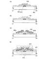
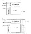
図2(A)は半導体装置の有する薄膜トランジスタ470の平面図であり、図2(B)は
図2(A)の線C1−C2における断面図である。薄膜トランジスタ470は逆スタガ型
の薄膜トランジスタであり、絶縁表面を有する基板である基板400上に、ゲート電極層
401、ゲート絶縁層402、半導体層403、ソース電極層又はドレイン電極層405
a、405bを含む。また、薄膜トランジスタ470を覆い、半導体層403に接する絶
縁膜407が設けられている。2A is a plan view of the
a, 405b. In addition, an insulating
半導体層403は、少なくとも絶縁膜407と接する領域が高抵抗化酸化物半導体領域で
あり、該高抵抗化酸化物半導体領域をチャネル形成領域として用いることができる。In the
高抵抗化酸化物半導体領域をチャネル形成領域として用いることによって、薄膜トランジ
スタの電気特性は安定化し、オフ電流の増加などを防止することができる。By using the high-resistance oxide semiconductor region as a channel formation region, the electrical characteristics of the thin film transistor can be stabilized and an increase in off-state current can be prevented.
なお、酸化物半導体層である半導体層403と接するソース電極層又はドレイン電極層4
05a、405bとして、酸素親和性の高い金属を含有する材料を用いていることが好ま
しい。上記酸素親和性の高い金属は、チタン、アルミニウム、マンガン、マグネシウム、
ジルコニウム、ベリリウム、トリウムのいずれか一または複数から選択された材料である
ことが好ましい。半導体層403と、酸素親和性の高い金属層とを接触させて熱処理を行
うと、半導体層403から金属層へと酸素原子が移動し、界面付近においてキャリア密度
が増加し低抵抗な領域が形成される。よって、薄膜トランジスタ470において、コンタ
クト抵抗が低く、オン電流は高くすることができる。該低抵抗な領域は界面を有する膜状
であってもよい。Note that the source or drain
As 05a and 405b, a material containing a metal having high oxygen affinity is preferably used. The metals with high oxygen affinity are titanium, aluminum, manganese, magnesium,
A material selected from one or more of zirconium, beryllium, and thorium is preferable. When heat treatment is performed by bringing the
従って、電気特性が良好で信頼性のよい薄膜トランジスタ470を有する半導体装置を作
製し、提供することが可能となる。Accordingly, a semiconductor device including the
チャネル形成領域を含む半導体層403としては、半導体特性を有する酸化物材料を用い
ればよい。例えば、InMO3(ZnO)m(m>0)で表記される構造の酸化物半導体
を用いることができ、特に、In−Ga−Zn−O系酸化物半導体を用いるのが好ましい
。なお、Mは、ガリウム(Ga)、鉄(Fe)、ニッケル(Ni)、マンガン(Mn)及
びコバルト(Co)から選ばれた一の金属元素又は複数の金属元素を示す。例えばMとし
て、Gaの場合があることの他、GaとNi又はGaとFeなど、Ga以外の上記金属元
素が含まれる場合がある。また、上記酸化物半導体において、Mとして含まれる金属元素
の他に、不純物元素としてFe、Niその他の遷移金属元素、又は該遷移金属の酸化物が
含まれているものがある。本明細書においては、InMO3(ZnO)m(m>0)で表
記される構造の酸化物半導体のうち、Mとして少なくともGaを含む構造の酸化物半導体
をIn−Ga−Zn−O系酸化物半導体と呼び、該薄膜をIn−Ga−Zn−O系非単結
晶膜とも呼ぶ。As the
また、酸化物半導体層に適用する酸化物半導体として上記の他にも、In−Sn−Zn−
O系、In−Al−Zn−O系、Sn−Ga−Zn−O系、Al−Ga−Zn−O系、S
n−Al−Zn−O系、In−Zn−O系、Sn−Zn−O系、Al−Zn−O系、In
−O系、Sn−O系、Zn−O系の酸化物半導体を適用することができる。また上記酸化
物半導体に酸化珪素を含ませてもよい。In addition to the above, an In—Sn—Zn— oxide semiconductor applied to the oxide semiconductor layer
O-based, In-Al-Zn-O-based, Sn-Ga-Zn-O-based, Al-Ga-Zn-O-based, S
n-Al-Zn-O, In-Zn-O, Sn-Zn-O, Al-Zn-O, In
An —O-based, Sn—O-based, or Zn—O-based oxide semiconductor can be used. Further, silicon oxide may be included in the oxide semiconductor.
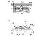
図2(A)乃至(D)に薄膜トランジスタ470の作製工程の断面図を示す。2A to 2D are cross-sectional views illustrating a manufacturing process of the
図2(A)において、絶縁表面を有する基板である基板400上にゲート電極層401を
設ける。下地膜となる絶縁膜を基板400とゲート電極層401の間に設けてもよい。下
地膜は、基板400からの不純物元素の拡散を防止する機能があり、窒化珪素膜、酸化珪
素膜、窒化酸化珪素膜、又は酸化窒化珪素膜から選ばれた一又は複数の膜による積層構造
により形成することができる。ゲート電極層401の材料は、モリブデン、チタン、クロ
ム、タンタル、タングステン、アルミニウム、銅、ネオジム、スカンジウム等の金属材料
又はこれらを主成分とする合金材料を用いて、単層で又は積層して形成することができる
。In FIG. 2A, a
例えば、ゲート電極層401の2層の積層構造としては、アルミニウム層上にモリブデン
層が積層された2層の積層構造、または銅層上にモリブデン層を積層した2層構造、また
は銅層上に窒化チタン層若しくは窒化タンタル層を積層した2層構造、窒化チタン層とモ
リブデン層とを積層した2層構造とすることが好ましい。3層の積層構造としては、タン
グステン層または窒化タングステン層と、アルミニウムとシリコンの合金層またはアルミ
ニウムとチタンの合金層と、窒化チタン層またはチタン層とを積層した積層とすることが
好ましい。For example, the two-layer structure of the
ゲート電極層401上にゲート絶縁層402を形成する。A
ゲート絶縁層402は、プラズマCVD法又はスパッタリング法等を用いて、酸化シリコ
ン層、窒化シリコン層、酸化窒化シリコン層又は窒化酸化シリコン層を単層で又は積層し
て形成することができる。例えば、成膜ガスとして、SiH4、酸素及び窒素を用いてプ
ラズマCVD法により酸化窒化シリコン層を形成すればよい。また、ゲート絶縁層402
として、有機シランガスを用いたCVD法により酸化シリコン層を形成することも可能で
ある。有機シランガスとしては、珪酸エチル(TEOS:化学式Si(OC2H5)4)
、テトラメチルシラン(TMS:化学式Si(CH3)4)、テトラメチルシクロテトラ
シロキサン(TMCTS)、オクタメチルシクロテトラシロキサン(OMCTS)、ヘキ
サメチルジシラザン(HMDS)、トリエトキシシラン(化学式SiH(OC2H5)3
)、トリスジメチルアミノシラン(化学式SiH(N(CH3)2)3)等のシリコン含
有化合物を用いることができる。The
It is also possible to form a silicon oxide layer by a CVD method using an organosilane gas. As the organosilane gas, ethyl silicate (TEOS: chemical formula Si (OC2 H5 )4 )
, Tetramethylsilane (TMS: chemical formula Si (CH3 )4 ), tetramethylcyclotetrasiloxane (TMCTS), octamethylcyclotetrasiloxane (OMCTS), hexamethyldisilazane (HMDS), triethoxysilane (chemical formula SiH (OC2 H5 )3
), Trisdimethylaminosilane (chemical formula SiH (N (CH3 )2 )3 ) and the like can be used.
ゲート絶縁層402上に、酸化物半導体膜を形成する。An oxide semiconductor film is formed over the
なお、酸化物半導体膜をスパッタ法により成膜する前に、アルゴンガスを導入してプラズ
マを発生させる逆スパッタを行い、ゲート絶縁層402の表面に付着しているゴミを除去
することが好ましい。逆スパッタとは、ターゲット側に電圧を印加せずに、アルゴン雰囲
気下で基板側にRF電源を用いて電圧を印加して基板近傍にプラズマを形成して表面を改
質する方法である。なお、アルゴン雰囲気に代えて窒素、ヘリウムなどを用いてもよい。
また、アルゴン雰囲気に酸素、N2Oなどを加えた雰囲気で行ってもよい。また、アルゴ
ン雰囲気にCl2、CF4などを加えた雰囲気で行ってもよい。Note that before the oxide semiconductor film is formed by a sputtering method, it is preferable to perform reverse sputtering in which an argon gas is introduced to generate plasma to remove dust attached to the surface of the
Alternatively, an argon atmosphere may be used in which oxygen, N2 O, or the like is added. Alternatively, an atmosphere obtained by adding Cl2 , CF4, or the like to an argon atmosphere may be used.
酸化物半導体膜としてIn−Ga−Zn−O系非単結晶膜を用いる。酸化物半導体膜は、
In−Ga−Zn−O系酸化物半導体ターゲットを用いてスパッタ法により成膜する。ま
た、酸化物半導体膜は、希ガス(代表的にはアルゴン)雰囲気下、酸素雰囲気下、又は希
ガス(代表的にはアルゴン)及び酸素雰囲気下においてスパッタ法により形成することが
できる。An In—Ga—Zn—O-based non-single-crystal film is used as the oxide semiconductor film. The oxide semiconductor film
A film is formed by a sputtering method using an In—Ga—Zn—O-based oxide semiconductor target. The oxide semiconductor film can be formed by a sputtering method in a rare gas (typically argon) atmosphere, an oxygen atmosphere, or a rare gas (typically argon) and oxygen atmosphere.
ゲート絶縁層402、及び酸化物半導体膜を大気に触れさせることなく連続的に形成して
もよい。大気に触れさせることなく連続成膜することで、界面が、水やハイドロカーボン
などの、大気成分や大気中に浮遊する不純物元素に汚染されることなく各積層界面を形成
することができるので、薄膜トランジスタ特性のばらつきを低減することができる。The
酸化物半導体膜をフォトリソグラフィ工程により島状の酸化物半導体層である酸化物半導
体層430(第1の酸化物半導体層)に加工する(図1(A)参照。)。The oxide semiconductor film is processed into an oxide semiconductor layer 430 (a first oxide semiconductor layer) which is an island-shaped oxide semiconductor layer by a photolithography process (see FIG. 1A).
酸化物半導体層430に窒素雰囲気下において加熱処理を行う。酸化物半導体層430は
窒素雰囲気下における加熱処理によって、低抵抗化(電気伝導率が高まる、好ましくは電
気伝導率1×10⁻¹S/cm以上1×102S/cm以下)し、低抵抗化した酸化物半
導体層431(第2の酸化物半導体層)とすることができる(図1(B)参照。)。Heat treatment is performed on the
窒素雰囲気下における酸化物半導体層430の加熱処理は温度200度以上で行うことが
好ましい。窒素雰囲気下における酸化物半導体層の加熱処理は、島状の酸化物半導体層4
30に加工する前の酸化物半導体膜に行ってもよい。The heat treatment of the
The oxide semiconductor film before being processed into 30 may be used.
ゲート絶縁層402、及び酸化物半導体層431上に導電膜を形成する。A conductive film is formed over the
導電膜の材料としては、Al、Cr、Ta、Ti、Mo、Wから選ばれた元素、または上
述した元素を成分とする合金か、上述した元素を組み合わせた合金膜等が挙げられる。Examples of the material for the conductive film include an element selected from Al, Cr, Ta, Ti, Mo, and W, an alloy containing the above-described element as a component, or an alloy film combining the above-described elements.
また、導電膜の材料としては、酸素親和性の高い金属であるチタン膜を用いると好ましい
。また、チタン膜上に上記Al、Cr、Ta、Mo、Wから選ばれた元素、または上述し
た元素を成分とする合金か、上述した元素を組み合わせた合金膜などを積層してもよい。As a material for the conductive film, a titanium film which is a metal with high oxygen affinity is preferably used. Further, an element selected from the above Al, Cr, Ta, Mo, and W, an alloy containing the above element as a component, or an alloy film combining the above elements may be stacked on the titanium film.
また、200℃〜600℃の熱処理を行う場合には、この熱処理に耐える耐熱性を導電膜
に持たせることが好ましい。Al単体では耐熱性が劣り、また腐蝕しやすい等の問題点が
あるので耐熱性導電性材料と組み合わせて形成する。Alと組み合わせる耐熱性導電性材
料としては、チタン(Ti)、タンタル(Ta)、タングステン(W)、モリブデン(M
o)、クロム(Cr)、ネオジム(Nd)、スカンジウム(Sc)から選ばれた元素、ま
たは上述した元素を成分とする合金か、上述した元素を組み合わせた合金膜、または上述
した元素を成分とする窒化物で形成する。In addition, when heat treatment at 200 ° C. to 600 ° C. is performed, it is preferable that the conductive film has heat resistance enough to withstand the heat treatment. Al alone is inferior in heat resistance and easily corroded, so it is formed in combination with a heat resistant conductive material. Examples of heat-resistant conductive materials combined with Al include titanium (Ti), tantalum (Ta), tungsten (W), and molybdenum (M
o), an element selected from chromium (Cr), neodymium (Nd), scandium (Sc), or an alloy containing the above elements as a component, an alloy film combining the above elements, or the above elements as components. Formed of nitride.
酸化物半導体層431、導電膜をエッチング工程によりエッチングし、酸化物半導体層4
32、及びソース電極層又はドレイン電極層405a、405bを形成する(図1(C)
参照。)。なお、酸化物半導体層431は一部のみがエッチングされ、溝部(凹部)を有
する酸化物半導体層432となる。The
32, and source or drain
reference. ). Note that only part of the
窒素雰囲気下における酸化物半導体層の加熱処理は、図28(A)乃至(D)のようにソ
ース電極層又はドレイン電極層405a、405bの形成後に行ってもよい。絶縁表面を
有する基板400上にゲート電極層401、ゲート絶縁層402、酸化物半導体層430
を形成する(図28(A)参照。)。酸化物半導体層430上にソース電極層又はドレイ
ン電極層405a、405bを形成し、酸化物半導体層430の一部エッチングして酸化
物半導体層441を形成する(図28(B)参照。)。次に酸化物半導体層441、及び
ソース電極層又はドレイン電極層405a、405bに窒素雰囲気下における加熱処理を
行う。その加熱処理によって酸化物半導体層441は低抵抗化され、低抵抗化した酸化物
半導体層432とすることができる(図28(C)参照。)。The heat treatment of the oxide semiconductor layer in a nitrogen atmosphere may be performed after formation of the source or drain
(See FIG. 28A). Source or
酸化物半導体層432に接してスパッタ法による酸化珪素膜を絶縁膜407として形成す
る。低抵抗化した酸化物半導体層432に接してスパッタ法により酸化珪素膜である絶縁
膜407を形成すると、低抵抗化した酸化物半導体層432において少なくとも酸化珪素
膜である絶縁膜407と接する領域を高抵抗化(電気伝導率が低まる)し、高抵抗化酸化
物半導体領域とすることができる。よって酸化物半導体層432は、高抵抗化酸化物半導
体領域を有する半導体層403(第3の酸化物半導体層)となり、薄膜トランジスタ47
0を作製することができる(図1(D)及び図28(D)参照。)。A silicon oxide film is formed as the insulating
0 can be manufactured (see FIGS. 1D and 28D).
絶縁膜407となる酸化珪素膜のスパッタ法による成膜は、希ガス(代表的にはアルゴン
)雰囲気下、酸素雰囲気下、又は希ガス(代表的にはアルゴン)及び酸素雰囲気下におい
て行うことができる。また、ターゲットとして酸化珪素ターゲットを用いても珪素ターゲ
ットを用いてもよい。例えば珪素ターゲットを用いて、酸素、及び窒素雰囲気下でスパッ
タ法により酸化珪素膜を形成することができる。The silicon oxide film to be the insulating
また、絶縁膜407となる酸化珪素膜を形成後、窒素雰囲気下、又は大気雰囲気下(大気
中)において薄膜トランジスタ470に加熱処理(好ましくは温度300度以下)を行っ
てもよい。例えば、窒素雰囲気下で350℃、1時間の熱処理を行う。該加熱処理を行う
と薄膜トランジスタ470の電気的特性のばらつきを軽減することができる。Alternatively, after the silicon oxide film to be the insulating
チャネル形成領域の半導体層は高抵抗化領域であるので、薄膜トランジスタの電気特性は
安定化し、オフ電流の増加などを防止することができる。よって、電気特性が良好で信頼
性のよい薄膜トランジスタを有する半導体装置とすることが可能となる。Since the semiconductor layer in the channel formation region is a high resistance region, the electrical characteristics of the thin film transistor can be stabilized and an increase in off current can be prevented. Therefore, a semiconductor device including a thin film transistor with favorable electric characteristics and high reliability can be obtained.
(実施の形態2)
半導体装置及び半導体装置の作製方法を図3及び図4を用いて説明する。実施の形態1と
同一部分又は同様な機能を有する部分、及び工程は、実施の形態1と同様に行うことがで
き、繰り返しの説明は省略する。(Embodiment 2)
A semiconductor device and a method for manufacturing the semiconductor device will be described with reference to FIGS. The same parts as those in
図4(A)は半導体装置の有する薄膜トランジスタ460の平面図であり、図4(B)は
図4(A)の線D1−D2における断面図である。薄膜トランジスタ460はボトムゲー
ト型の薄膜トランジスタであり、絶縁表面を有する基板である基板450上に、ゲート電
極層451、ゲート絶縁層452、ソース電極層又はドレイン電極層455a、455b
、及び半導体層453を含む。また、薄膜トランジスタ460を覆い、半導体層453に
接する絶縁膜457が設けられている。半導体層453は、In−Ga−Zn−O系非単
結晶膜を用いる。4A is a plan view of the
And a
薄膜トランジスタ460は、薄膜トランジスタ460を含む領域全てにおいてゲート絶縁
層452が存在し、ゲート絶縁層452と絶縁表面を有する基板である基板450の間に
ゲート電極層451が設けられている。ゲート絶縁層452上にはソース電極層又はドレ
イン電極層455a、455bが設けられている。そして、ゲート絶縁層452、及びソ
ース電極層又はドレイン電極層455a、455b上に半導体層453が設けられている
。また、図示しないが、ゲート絶縁層452上にはソース電極層又はドレイン電極層45
5a、455bに加えて配線層を有し、該配線層は半導体層453の外周部より外側に延
在している。In the
In addition to 5a and 455b, a wiring layer is provided, and the wiring layer extends outside the outer peripheral portion of the
半導体層453は、少なくとも絶縁膜457と接する領域が高抵抗化酸化物半導体領域で
あり、該高抵抗化酸化物半導体領域をチャネル形成領域をとして用いることができる。In the
高抵抗化酸化物半導体領域をチャネル形成領域として用いることによって、薄膜トランジ
スタの電気特性は安定化し、オフ電流の増加などを防止することができる。By using the high-resistance oxide semiconductor region as a channel formation region, the electrical characteristics of the thin film transistor can be stabilized and an increase in off-state current can be prevented.
なお、酸化物半導体層である半導体層453と接するソース電極層又はドレイン電極層4
55a、455bとして、酸素親和性の高い金属を含有する材料を用いていることが好ま
しい。上記酸素親和性の高い金属は、チタン、アルミニウム、マンガン、マグネシウム、
ジルコニウム、ベリリウム、トリウムのいずれか一または複数から選択された材料である
ことが好ましい。半導体層453と、酸素親和性の高い金属層とを接触させて熱処理を行
うと、半導体層453から金属層へと酸素原子が移動し、界面付近においてキャリア密度
が増加し低抵抗な領域が形成される。よって、薄膜トランジスタ460において、コンタ
クト抵抗が低く、オン電流は高くすることができる。該低抵抗な領域は界面を有する膜状
であってもよい。Note that the source or drain
As 55a and 455b, it is preferable to use a material containing a metal with high oxygen affinity. The metals with high oxygen affinity are titanium, aluminum, manganese, magnesium,
A material selected from one or more of zirconium, beryllium, and thorium is preferable. When heat treatment is performed by bringing the
従って、電気特性が良好で信頼性のよい薄膜トランジスタ460を有する半導体装置を作
製し、提供することが可能となる。Accordingly, a semiconductor device including the
図3(A)乃至(D)に薄膜トランジスタ460の作製工程の断面図を示す。3A to 3D are cross-sectional views illustrating a manufacturing process of the
絶縁表面を有する基板である基板450上にゲート電極層451を設ける。下地膜となる
絶縁膜を基板450とゲート電極層451の間に設けてもよい。下地膜は、基板450か
らの不純物元素の拡散を防止する機能があり、窒化珪素膜、酸化珪素膜、窒化酸化珪素膜
、又は酸化窒化珪素膜から選ばれた一又は複数の膜による積層構造により形成することが
できる。ゲート電極層451の材料は、モリブデン、チタン、クロム、タンタル、タング
ステン、アルミニウム、銅、ネオジム、スカンジウム等の金属材料又はこれらを主成分と
する合金材料を用いて、単層で又は積層して形成することができる。A
ゲート電極層451上にゲート絶縁層452を形成する。A
ゲート絶縁層452は、プラズマCVD法又はスパッタリング法等を用いて、酸化シリコ
ン層、窒化シリコン層、酸化窒化シリコン層又は窒化酸化シリコン層を単層で又は積層し
て形成することができる。また、また、ゲート絶縁層452として、有機シランガスを用
いたCVD法により酸化シリコン層を形成することも可能である。The
ゲート絶縁層452上に、導電膜を形成し、フォトリソグラフィ工程により島状のソース
電極層又はドレイン電極層455a、455bに加工する(図3(A)参照。)。A conductive film is formed over the
ソース電極層又はドレイン電極層455a、455bの材料としては、Al、Cr、Ta
、Ti、Mo、Wから選ばれた元素、または上述した元素を成分とする合金か、上述した
元素を組み合わせた合金膜等が挙げられる。As the material of the source electrode layer or
An element selected from Ti, Mo, W, an alloy containing the above-described element as a component, an alloy film combining the above-described elements, or the like can be given.
また、ソース電極層又はドレイン電極層455a、455bの材料としては、酸素親和性
の高い金属であるチタン膜を用いると好ましい。また、チタン膜上にAl、Cr、Ta、
Mo、Wから選ばれた元素、または上述した元素を成分とする合金か、上述した元素を組
み合わせた合金膜などを積層してもよい。As a material for the source or drain
You may laminate | stack the alloy film etc. which combined the element chosen from the element chosen from Mo and W, the element mentioned above, or the element mentioned above.
また、200℃〜600℃の熱処理を行う場合には、この熱処理に耐える耐熱性を導電膜
に持たせることが好ましい。Al単体では耐熱性が劣り、また腐蝕しやすい等の問題点が
あるので耐熱性導電性材料と組み合わせて形成する。Alと組み合わせる耐熱性導電性材
料としては、チタン(Ti)、タンタル(Ta)、タングステン(W)、モリブデン(M
o)、クロム(Cr)、ネオジム(Nd)、スカンジウム(Sc)から選ばれた元素、ま
たは上述した元素を成分とする合金か、上述した元素を組み合わせた合金膜、または上述
した元素を成分とする窒化物で形成する。In addition, when heat treatment at 200 ° C. to 600 ° C. is performed, it is preferable that the conductive film has heat resistance enough to withstand the heat treatment. Al alone is inferior in heat resistance and easily corroded, so it is formed in combination with a heat resistant conductive material. Examples of heat-resistant conductive materials combined with Al include titanium (Ti), tantalum (Ta), tungsten (W), and molybdenum (M
o), an element selected from chromium (Cr), neodymium (Nd), scandium (Sc), or an alloy containing the above elements as a component, an alloy film combining the above elements, or the above elements as components. Formed of nitride.
次に、ゲート絶縁層452、及びソース電極層又はドレイン電極層455a、455b上
に酸化物半導体膜を形成し、フォトリソグラフィ工程により島状の酸化物半導体層483
(第1の酸化物半導体層)に加工する(図3(B)参照。)。Next, an oxide semiconductor film is formed over the
The first oxide semiconductor layer is processed (see FIG. 3B).
酸化物半導体層483は、チャネル形成領域となるため、実施の形態1の酸化物半導体膜
と同様に形成する。Since the
なお、酸化物半導体層483をスパッタ法により成膜する前に、アルゴンガスを導入して
プラズマを発生させる逆スパッタを行い、ゲート絶縁層452の表面に付着しているゴミ
を除去することが好ましい。Note that before the
酸化物半導体層483に窒素雰囲気下において加熱処理を行う。酸化物半導体層483は
窒素雰囲気下における加熱処理によって、低抵抗化(電気伝導率が高まる、好ましくは電
気伝導率1×10⁻¹S/cm以上1×102S/cm以下)し、低抵抗化した酸化物半
導体層484(第2の酸化物半導体層)とすることができる(図3(C)参照。)。Heat treatment is performed on the
窒素雰囲気下における酸化物半導体層483の加熱処理は温度200度以上で行うことが
好ましい。The heat treatment of the
酸化物半導体層484に接してスパッタ法による酸化珪素膜を絶縁膜457として形成す
る。低抵抗化した酸化物半導体層484に接してスパッタ法により酸化珪素膜である絶縁
膜457を形成すると、低抵抗化した酸化物半導体層484において少なくとも酸化珪素
膜である絶縁膜457と接する領域を高抵抗化(電気伝導率が低まる)し、高抵抗化酸化
物半導体領域とすることができる。よって酸化物半導体層484は、高抵抗化酸化物半導
体領域を有する半導体層453(第3の酸化物半導体層)となり、薄膜トランジスタ46
0を作製することができる(図3(D)参照。)。A silicon oxide film is formed as the insulating
0 can be manufactured (see FIG. 3D).
絶縁膜457となる酸化珪素膜のスパッタ法による成膜は、希ガス(代表的にはアルゴン
)雰囲気下、酸素雰囲気下、又は希ガス(代表的にはアルゴン)及び酸素雰囲気下におい
て行うことができる。また、ターゲットとして酸化珪素ターゲットを用いても珪素ターゲ
ットを用いてもよい。例えば珪素ターゲットを用いて、酸素、及び窒素雰囲気下でスパッ
タ法により酸化珪素膜を形成することができる。The silicon oxide film to be the insulating
また、絶縁膜457となる酸化珪素膜を形成後、窒素雰囲気下、又は大気雰囲気下(大気
中)において薄膜トランジスタ460に加熱処理(好ましくは温度300度以下)を行っ
てもよい。例えば、窒素雰囲気下で350℃、1時間の熱処理を行う。該加熱処理を行う
と薄膜トランジスタ460の電気的特性のばらつきを軽減することができる。Alternatively, after the silicon oxide film to be the insulating
チャネル形成領域の半導体層は高抵抗化領域であるので、薄膜トランジスタの電気特性は
安定化し、オフ電流の増加などを防止することができる。よって、電気特性が良好で信頼
性のよい薄膜トランジスタを有する半導体装置とすることが可能となる。Since the semiconductor layer in the channel formation region is a high resistance region, the electrical characteristics of the thin film transistor can be stabilized and an increase in off current can be prevented. Therefore, a semiconductor device including a thin film transistor with favorable electric characteristics and high reliability can be obtained.
(実施の形態3)
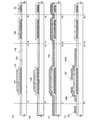
薄膜トランジスタを含む半導体装置の作製工程について、図5乃至図8を用いて説明する
。(Embodiment 3)
A manufacturing process of a semiconductor device including a thin film transistor will be described with reference to FIGS.
図5(A)において、透光性を有する基板100にはバリウムホウケイ酸ガラスやアルミ
ノホウケイ酸ガラスなどのガラス基板を用いることができる。In FIG. 5A, a glass substrate such as barium borosilicate glass or alumino borosilicate glass can be used for the light-transmitting
次いで、導電層を基板100全面に形成した後、第1のフォトリソグラフィ工程を行い、
レジストマスクを形成し、エッチングにより不要な部分を除去して配線及び電極(ゲート
電極層101を含むゲート配線、容量配線108、及び第1の端子121)を形成する。
このとき少なくともゲート電極層101の端部にテーパー形状が形成されるようにエッチ
ングする。Next, after a conductive layer is formed on the entire surface of the
A resist mask is formed, unnecessary portions are removed by etching, and wirings and electrodes (a gate wiring including the
At this time, etching is performed so that at least an end portion of the
ゲート電極層101を含むゲート配線と容量配線108、端子部の第1の端子121は、
耐熱性導電性材料としては、チタン(Ti)、タンタル(Ta)、タングステン(W)、
モリブデン(Mo)、クロム(Cr)、Nd(ネオジム)、スカンジウム(Sc)から選
ばれた元素、または上述した元素を成分とする合金か、上述した元素を組み合わせた合金
膜、または上述した元素を成分とする窒化物で形成することが望ましい。また、アルミニ
ウム(Al)や銅(Cu)などの低抵抗導電性材料で形成する場合は、Al単体又はCu
単体では耐熱性が劣り、また腐蝕しやすい等の問題点があるので上記耐熱性導電性材料と
組み合わせて形成する。The gate wiring including the
Examples of heat-resistant conductive materials include titanium (Ti), tantalum (Ta), tungsten (W),
An element selected from molybdenum (Mo), chromium (Cr), Nd (neodymium), scandium (Sc), an alloy containing the above-described element as a component, an alloy film combining the above-described elements, or the above-described element It is desirable to form with nitride as a component. In addition, when formed of a low resistance conductive material such as aluminum (Al) or copper (Cu), Al alone or Cu
Since the simple substance has poor heat resistance and is susceptible to corrosion, it is formed in combination with the above heat resistant conductive material.
次いで、ゲート電極層101上にゲート絶縁層102を全面に成膜する。ゲート絶縁層1
02はスパッタ法、CVD法などを用い、膜厚を50〜250nmとする。Next, the
02 uses a sputtering method, a CVD method, or the like, and has a film thickness of 50 to 250 nm.
例えば、ゲート絶縁層102としてスパッタ法により酸化シリコン膜を用い、100nm
の厚さで形成する。勿論、ゲート絶縁層102はこのような酸化シリコン膜に限定される
ものでなく、酸化窒化シリコン膜、窒化シリコン膜、酸化アルミニウム膜、酸化タンタル
膜などの他の絶縁膜を用い、これらの材料から成る単層または積層構造として形成しても
良い。For example, a silicon oxide film is used as the
The thickness is formed. Needless to say, the
次に、ゲート絶縁層102上に、酸化物半導体膜(In−Ga−Zn−O系非単結晶膜)
を成膜する。プラズマ処理後、大気に曝すことなくIn−Ga−Zn−O系非単結晶膜を
成膜することは、ゲート絶縁層と半導体膜の界面にゴミや水分を付着させない点で有用で
ある。ここでは、直径8インチのIn、Ga、及びZnを含む酸化物半導体ターゲット(
In−Ga−Zn−O系酸化物半導体ターゲット(In2O3:Ga2O3:ZnO=1
:1:1[mol比]))を用いて、基板とターゲットの間との距離を170mm、圧力
0.4Pa、直流(DC)電源0.5kW、酸素のみ、アルゴンのみ、又はアルゴン及び
酸素雰囲気下で成膜する。なお、パルス直流(DC)電源を用いると、ごみが軽減でき、
膜厚分布も均一となるために好ましい。In−Ga−Zn−O系非単結晶膜の膜厚は、5
nm〜200nmとする。酸化物半導体膜として、In−Ga−Zn−O系酸化物半導体
ターゲットを用いてスパッタ法により膜厚50nmのIn−Ga−Zn−O系非単結晶膜
を成膜する。Next, an oxide semiconductor film (In—Ga—Zn—O-based non-single-crystal film) is formed over the
Is deposited. After the plasma treatment, forming an In—Ga—Zn—O-based non-single-crystal film without exposure to the air is useful in that dust and moisture are not attached to the interface between the gate insulating layer and the semiconductor film. Here, an oxide semiconductor target containing In, Ga, and Zn having a diameter of 8 inches (
In—Ga—Zn—O-based oxide semiconductor target (In2 O3 : Ga2 O3 : ZnO = 1)
: 1: 1 [mol ratio])), the distance between the substrate and the target is 170 mm, pressure 0.4 Pa, direct current (DC) power supply 0.5 kW, oxygen only, argon only, or argon and oxygen atmosphere The film is formed below. Using a pulsed direct current (DC) power supply can reduce dust,
It is preferable because the film thickness distribution is uniform. The thickness of the In—Ga—Zn—O-based non-single-crystal film is 5
nm to 200 nm. As the oxide semiconductor film, an In—Ga—Zn—O-based non-single-crystal film with a thickness of 50 nm is formed by a sputtering method using an In—Ga—Zn—O-based oxide semiconductor target.
スパッタ法にはスパッタ用電源に高周波電源を用いるRFスパッタ法と、DCスパッタ法
があり、さらにパルス的にバイアスを与えるパルスDCスパッタ法もある。RFスパッタ
法は主に絶縁膜を成膜する場合に用いられ、DCスパッタ法は主に金属膜を成膜する場合
に用いられる。Sputtering methods include an RF sputtering method using a high frequency power source as a sputtering power source and a DC sputtering method, and also a pulsed DC sputtering method that applies a bias in a pulsed manner. The RF sputtering method is mainly used when an insulating film is formed, and the DC sputtering method is mainly used when a metal film is formed.
また、材料の異なるターゲットを複数設置できる多元スパッタ装置もある。多元スパッタ
装置は、同一チャンバーで異なる材料膜を積層成膜することも、同一チャンバーで複数種
類の材料を同時に放電させて成膜することもできる。There is also a multi-source sputtering apparatus in which a plurality of targets of different materials can be installed. The multi-source sputtering apparatus can be formed by stacking different material films in the same chamber, or by simultaneously discharging a plurality of types of materials in the same chamber.
また、チャンバー内部に磁石機構を備えたマグネトロンスパッタ法を用いるスパッタ装置
や、グロー放電を使わずマイクロ波を用いて発生させたプラズマを用いるECRスパッタ
法を用いるスパッタ装置がある。Further, there is a sputtering apparatus using a magnetron sputtering method having a magnet mechanism inside a chamber, and a sputtering apparatus using an ECR sputtering method using plasma generated using microwaves without using glow discharge.
また、スパッタ法を用いる成膜方法として、成膜中にターゲット物質とスパッタガス成分
とを化学反応させてそれらの化合物薄膜を形成するリアクティブスパッタ法や、成膜中に
基板にも電圧をかけるバイアススパッタ法もある。In addition, as a film formation method using a sputtering method, a reactive sputtering method in which a target material and a sputtering gas component are chemically reacted during film formation to form a compound thin film thereof, or a voltage is applied to the substrate during film formation. There is also a bias sputtering method.
次に、第2のフォトリソグラフィ工程を行い、レジストマスクを形成し、酸化物半導体膜
をエッチングする。例えば燐酸と酢酸と硝酸を混ぜた溶液を用いたウェットエッチングに
より、不要な部分を除去して酸化物半導体層133を形成する。なお、ここでのエッチン
グは、ウェットエッチングに限定されずドライエッチングを用いてもよい。Next, a second photolithography step is performed to form a resist mask, and the oxide semiconductor film is etched. For example, unnecessary portions are removed by wet etching using a mixed solution of phosphoric acid, acetic acid, and nitric acid, so that the
ドライエッチングに用いるエッチングガスとしては、塩素を含むガス(塩素系ガス、例え
ば塩素(Cl2)、塩化硼素(BCl3)、塩化珪素(SiCl4)、四塩化炭素(CC
l4)など)が好ましい。As an etching gas used for dry etching, a gas containing chlorine (chlorine-based gas such as chlorine (Cl2 ), boron chloride (BCl3 ), silicon chloride (SiCl4 ), carbon tetrachloride (CC
l4 ) etc. are preferred.
また、フッ素を含むガス(フッ素系ガス、例えば四弗化炭素(CF4)、弗化硫黄(SF
6)、弗化窒素(NF3)、トリフルオロメタン(CHF3)など)、臭化水素(HBr
)、酸素(O2)、これらのガスにヘリウム(He)やアルゴン(Ar)などの希ガスを
添加したガス、などを用いることができる。Gases containing fluorine (fluorine-based gases such as carbon tetrafluoride (CF4 ), sulfur fluoride (SF
6 ), nitrogen fluoride (NF3 ), trifluoromethane (CHF3 ), etc.), hydrogen bromide (HBr
), Oxygen (O2 ), a gas obtained by adding a rare gas such as helium (He) or argon (Ar) to these gases, or the like can be used.
ドライエッチング法としては、平行平板型RIE(Reactive Ion Etch
ing)法や、ICP(Inductively Coupled Plasma:誘導
結合型プラズマ)エッチング法を用いることができる。所望の加工形状にエッチングでき
るように、エッチング条件(コイル型の電極に印加される電力量、基板側の電極に印加さ
れる電力量、基板側の電極温度等)を適宜調節する。As a dry etching method, parallel plate RIE (Reactive Ion Etch) is used.
ing) method or ICP (Inductively Coupled Plasma) etching method can be used. Etching conditions (such as the amount of power applied to the coil-type electrode, the amount of power applied to the substrate-side electrode, the substrate-side electrode temperature, etc.) are adjusted as appropriate so that the desired processed shape can be etched.
ウエットエッチングに用いるエッチング液としては、燐酸と酢酸と硝酸を混ぜた溶液、ア
ンモニア過水(過酸化水素:アンモニア:水=5:2:2)などを用いることができる。
また、ITO07N(関東化学社製)を用いてもよい。As an etchant used for wet etching, a mixed solution of phosphoric acid, acetic acid, and nitric acid, ammonia perwater (hydrogen peroxide: ammonia: water = 5: 2: 2), or the like can be used.
In addition, ITO07N (manufactured by Kanto Chemical Co., Inc.) may be used.
また、ウエットエッチング後のエッチング液はエッチングされた材料とともに洗浄によっ
て除去される。その除去された材料を含むエッチング液の廃液を精製し、含まれる材料を
再利用してもよい。当該エッチング後の廃液から酸化物半導体層に含まれるインジウム等
の材料を回収して再利用することにより、資源を有効活用し低コスト化することができる
。Further, the etchant after the wet etching is removed by washing together with the etched material. The waste solution of the etching solution containing the removed material may be purified and the contained material may be reused. By recovering and reusing materials such as indium contained in the oxide semiconductor layer from the waste liquid after the etching, resources can be effectively used and costs can be reduced.
所望の加工形状にエッチングできるように、材料に合わせてエッチング条件(エッチング
液、エッチング時間、温度等)を適宜調節する。Etching conditions (such as an etchant, etching time, and temperature) are adjusted as appropriate depending on the material so that the material can be etched into a desired shape.
次に、酸化物半導体層133に窒素雰囲気下で加熱処理を行う。Next, heat treatment is performed on the
加熱処理は、200℃以上で行うと良い。例えば、窒素雰囲気下で350℃、1時間の熱
処理を行う。この窒素雰囲気下の加熱処理により、酸化物半導体層133は、低抵抗化し
導電率が高まる。よって低抵抗化した酸化物半導体層134が形成される(図5(B)参
照。)。酸化物半導体層134の電気伝導率は1×10⁻¹S/cm以上1×102S/
cm以下が好ましい。なお、この加熱処理は、ソース電極層及びドレイン電極層を形成後
に行ってもよい。The heat treatment is preferably performed at 200 ° C. or higher. For example, heat treatment is performed at 350 ° C. for 1 hour in a nitrogen atmosphere. By the heat treatment under the nitrogen atmosphere, the
cm or less is preferable. Note that this heat treatment may be performed after the source electrode layer and the drain electrode layer are formed.
次に、酸化物半導体層134上に金属材料からなる導電膜132をスパッタ法や真空蒸着
法で形成する(図5(C)参照。)。Next, a
導電膜132の材料としては、Al、Cr、Ta、Ti、Mo、Wから選ばれた元素、ま
たは上述した元素を成分とする合金か、上述した元素を組み合わせた合金膜等が挙げられ
る。Examples of the material of the
また、200℃〜600℃の熱処理を行う場合には、この熱処理に耐える耐熱性を導電膜
に持たせることが好ましい。Al単体では耐熱性が劣り、また腐蝕しやすい等の問題点が
あるので耐熱性導電性材料と組み合わせて形成する。Alと組み合わせる耐熱性導電性材
料としては、チタン(Ti)、タンタル(Ta)、タングステン(W)、モリブデン(M
o)、クロム(Cr)、ネオジム(Nd)、スカンジウム(Sc)から選ばれた元素、ま
たは上述した元素を成分とする合金か、上述した元素を組み合わせた合金膜、または上述
した元素を成分とする窒化物で形成する。In addition, when heat treatment at 200 ° C. to 600 ° C. is performed, it is preferable that the conductive film has heat resistance enough to withstand the heat treatment. Al alone is inferior in heat resistance and easily corroded, so it is formed in combination with a heat resistant conductive material. Examples of heat-resistant conductive materials combined with Al include titanium (Ti), tantalum (Ta), tungsten (W), and molybdenum (M
o), an element selected from chromium (Cr), neodymium (Nd), scandium (Sc), or an alloy containing the above elements as a component, an alloy film combining the above elements, or the above elements as components. Formed of nitride.
導電膜132として酸素親和性の高い金属であるチタン膜を用いると好ましい。また、導
電膜132は、2層構造としてもよく、アルミニウム膜上にチタン膜を積層してもよい。
また、導電膜132としてTi膜と、そのTi膜上に重ねてNdを含むアルミニウム(A
l−Nd)膜を積層し、さらにその上にTi膜を成膜する3層構造としてもよい。導電膜
132は、シリコンを含むアルミニウム膜の単層構造としてもよい。As the
In addition, as the
l-Nd) films may be stacked, and a Ti film may be formed thereon. The
次に、第3のフォトリソグラフィ工程を行い、レジストマスクを形成し、エッチングによ
り不要な部分を除去してソース電極層又はドレイン電極層105a、105b、及び第2
の端子122を形成する(図5(D)参照。)。この際のエッチング方法としてウェット
エッチングまたはドライエッチングを用いる。例えば導電膜132としてアルミニウム膜
、又はアルミニウム合金膜を用いる場合は、燐酸と酢酸と硝酸を混ぜた溶液を用いたウェ
ットエッチングを行うことができる。また、アンモニア過水(過酸化水素:アンモニア:
水=5:2:2)を用いたウェットエッチングにより、導電膜132をエッチングしてソ
ース電極層又はドレイン電極層105a、105bを形成してもよい。このエッチング工
程において、酸化物半導体層134の露出領域も一部エッチングされ、半導体層135と
なる。よってソース電極層又はドレイン電極層105a、105bの間の半導体層135
は膜厚の薄い領域となる。図5(D)においては、ソース電極層又はドレイン電極層10
5a、105b、半導体層135のエッチングをドライエッチングによって一度に行うた
め、ソース電極層又はドレイン電極層105a、105b及び半導体層135の端部は一
致し、連続的な構造となっている。Next, a third photolithography step is performed, a resist mask is formed, unnecessary portions are removed by etching, and the source or drain
The terminal 122 is formed (see FIG. 5D). As an etching method at this time, wet etching or dry etching is used. For example, in the case where an aluminum film or an aluminum alloy film is used as the
The
Is a thin region. In FIG. 5D, the source or drain
Since the etching of 5a, 105b and the
また、この第3のフォトリソグラフィ工程において、ソース電極層又はドレイン電極層1
05a、105bと同じ材料である第2の端子122を端子部に残す。なお、第2の端子
122はソース配線(ソース電極層又はドレイン電極層105a、105bを含むソース
配線)と電気的に接続されている。In the third photolithography step, the source electrode layer or the
The
また、多階調マスクにより形成した複数(代表的には二種類)の厚さの領域を有するレジ
ストマスクを用いると、レジストマスクの数を減らすことができるため、工程簡略化、低
コスト化が図れる。In addition, when a resist mask having a plurality of (typically two types) thickness regions formed using a multi-tone mask is used, the number of resist masks can be reduced, which simplifies processes and reduces costs. I can plan.
ここで、酸化物半導体層である半導体層135及びソース電極層又はドレイン電極層10
5a、105bに加熱処理を行ってもよい。ソース電極層又はドレイン電極層105a、
105bに酸素親和性の高い金属を用いると、この加熱処理により酸化物半導体層からソ
ース電極層又はドレイン電極層105a、105bへと酸素原子が移動するので、ソース
電極層又はドレイン電極層105a、105と接する領域を低抵抗化領域とすることがで
きる。このソース電極層又はドレイン電極層105a、105と、半導体層135との間
に形成される低抵抗領域は、界面を有する膜状であってもよい。Here, the
You may heat-process to 5a, 105b. A source or drain
When a metal having a high oxygen affinity is used for 105b, oxygen atoms move from the oxide semiconductor layer to the source or drain
次に、ゲート絶縁層102、酸化物半導体層135、ソース電極層又はドレイン電極層1
05a、105bを覆う保護絶縁層107を形成する。保護絶縁層107はスパッタ法に
より形成する酸化シリコン膜を用いる。ソース電極層又はドレイン電極層105a、10
5bの間に設けられた酸化物半導体層135の露出領域と保護絶縁層107である酸化珪
素膜が接して設けられることによって、保護絶縁層107と接する酸化物半導体層135
の領域が高抵抗化(電気伝導度が低まる)し、高抵抗化したチャネル形成領域を有する半
導体層103を形成することができる(図6(A)参照。)。Next, the
A protective insulating
The exposed region of the
This region has a higher resistance (lower electrical conductivity), so that the
以上の工程で薄膜トランジスタ170が作製できる。Through the above process, the
薄膜トランジスタ170の形成後、加熱処理を行ってもよい。加熱処理は酸素雰囲気下、
又は窒素雰囲気下において、300度以上で行えばよい。この加熱処理により薄膜トラン
ジスタの電気特性のばらつきを軽減することができる。Heat treatment may be performed after the
Alternatively, it may be performed at 300 ° C. or higher in a nitrogen atmosphere. By this heat treatment, variation in electrical characteristics of the thin film transistor can be reduced.
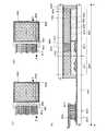
次に、第4のフォトリソグラフィ工程を行い、レジストマスクを形成し、保護絶縁層10
7及びゲート絶縁層102のエッチングによりソース電極層又はドレイン電極層105b
に達するコンタクトホール125を形成する。また、ここでのエッチングにより第2の端
子122に達するコンタクトホール127、第1の端子121に達するコンタクトホール
126も形成する。この段階での断面図を図6(B)に示す。Next, a fourth photolithography step is performed to form a resist mask, and the protective insulating
7 and the
A
次いで、レジストマスクを除去した後、透明導電膜を成膜する。透明導電膜の材料として
は、酸化インジウム(In2O3)や酸化インジウム酸化スズ合金(In2O3―SnO
2、ITOと略記する)などをスパッタ法や真空蒸着法などを用いて形成する。このよう
な材料のエッチング処理は塩酸系の溶液により行う。しかし、特にITOのエッチングは
残渣が発生しやすいので、エッチング加工性を改善するために酸化インジウム酸化亜鉛合
金(In2O3―ZnO)を用いても良い。Next, after removing the resist mask, a transparent conductive film is formed. As a material of the transparent conductive film, indium oxide (In2 O3 ) or indium tin oxide alloy (In2 O3 —SnO) is used.
2 is abbreviated as ITO) using a sputtering method, a vacuum deposition method, or the like. Etching treatment of such a material is performed with a hydrochloric acid based solution. However, in particular, since etching of ITO is likely to generate a residue, an indium oxide-zinc oxide alloy (In2 O3 —ZnO) may be used to improve etching processability.
次に、第5のフォトリソグラフィ工程を行い、レジストマスクを形成し、エッチングによ
り不要な部分を除去して画素電極層110を形成する。Next, a fifth photolithography step is performed to form a resist mask, and unnecessary portions are removed by etching, so that the
また、この第5のフォトリソグラフィ工程において、容量部におけるゲート絶縁層102
及び保護絶縁層107を誘電体として、容量配線108と画素電極層110とで保持容量
が形成される。In the fifth photolithography step, the
The
また、この第5のフォトリソグラフィ工程において、第1の端子121及び第2の端子1
22をレジストマスクで覆い端子部に形成された透明導電膜128、129を残す。透明
導電膜128、129はFPCとの接続に用いられる電極または配線となる。第1の端子
121上に形成された透明導電膜128は、ゲート配線の入力端子として機能する接続用
の端子電極となる。第2の端子122上に形成された透明導電膜129は、ソース配線の
入力端子として機能する接続用の端子電極である。In the fifth photolithography step, the
22 is covered with a resist mask, and the transparent
次いで、レジストマスクを除去し、この段階での断面図を図6(C)に示す。なお、この
段階での平面図が図7に相当する。Next, the resist mask is removed, and a cross-sectional view at this stage is illustrated in FIG. Note that a plan view at this stage corresponds to FIG.
また、図8(A1)、図8(A2)は、この段階でのゲート配線端子部の平面図及び断面
図をそれぞれ図示している。図8(A1)は図8(A2)中のE1−E2線に沿った断面
図に相当する。図8(A1)において、保護絶縁膜154上に形成される透明導電膜15
5は、入力端子として機能する接続用の端子電極である。また、図8(A1)において、
端子部では、ゲート配線と同じ材料で形成される第1の端子151と、ソース配線と同じ
材料で形成される接続電極層153とがゲート絶縁層152を介して重なり、透明導電膜
155で導通させている。なお、図6(C)に図示した透明導電膜128と第1の端子1
21とが接触している部分が、図8(A1)の透明導電膜155と第1の端子151が接
触している部分に対応している。8A1 and 8A2 are a plan view and a cross-sectional view of the gate wiring terminal portion at this stage, respectively. FIG. 8A1 corresponds to a cross-sectional view taken along line E1-E2 in FIG. In FIG. 8A1, the transparent
In the terminal portion, the
A portion in contact with 21 corresponds to a portion in which the transparent
また、図8(B1)、及び図8(B2)は、図6(C)に示すソース配線端子部とは異な
るソース配線端子部の断面図及び平面図をそれぞれ図示している。また、図8(B1)は
図8(B2)中のF1−F2線に沿った断面図に相当する。図8(B1)において、保護
絶縁膜154上に形成される透明導電膜155は、入力端子として機能する接続用の端子
電極である。また、図8(B1)において、端子部では、ゲート配線と同じ材料で形成さ
れる電極層156が、ソース配線と電気的に接続される第2の端子150の下方にゲート
絶縁層152を介して重なる。電極層156は第2の端子150とは電気的に接続してお
らず、電極層156を第2の端子150と異なる電位、例えばフローティング、GND、
0Vなどに設定すれば、ノイズ対策のための容量または静電気対策のための容量を形成す
ることができる。また、第2の端子150は、保護絶縁膜154を介して透明導電膜15
5と電気的に接続している。8B1 and 8B2 are a cross-sectional view and a plan view of a source wiring terminal portion different from the source wiring terminal portion shown in FIG. 6C, respectively. 8B1 corresponds to a cross-sectional view taken along line F1-F2 in FIG. 8B2. In FIG. 8B1, a transparent
If set to 0 V or the like, it is possible to form a capacitor for noise countermeasures or a capacitor for static electricity countermeasures. The
5 is electrically connected.
ゲート配線、ソース配線、及び容量配線は画素密度に応じて複数本設けられるものである
。また、端子部においては、ゲート配線と同電位の第1の端子、ソース配線と同電位の第
2の端子、容量配線と同電位の第3の端子などが複数並べられて配置される。それぞれの
端子の数は、それぞれ任意な数で設ければ良いものとし、実施者が適宣決定すれば良い。A plurality of gate wirings, source wirings, and capacitor wirings are provided depending on the pixel density. In the terminal portion, a plurality of first terminals having the same potential as the gate wiring, second terminals having the same potential as the source wiring, third terminals having the same potential as the capacitor wiring, and the like are arranged. Any number of terminals may be provided, and the practitioner may determine the number appropriately.
こうして5回のフォトリソグラフィ工程により、5枚のフォトマスクを使用して、ボトム
ゲート型のスタガ構造の薄膜トランジスタである薄膜トランジスタ170を有する画素薄
膜トランジスタ部、保持容量を完成させることができる。そして、これらを個々の画素に
対応してマトリクス状に配置して画素部を構成することによりアクティブマトリクス型の
表示装置を作製するための一方の基板とすることができる。本明細書では便宜上このよう
な基板をアクティブマトリクス基板と呼ぶ。In this manner, the pixel thin film transistor portion and the storage capacitor having the
アクティブマトリクス型の液晶表示装置を作製する場合には、アクティブマトリクス基板
と、対向電極が設けられた対向基板との間に液晶層を設け、アクティブマトリクス基板と
対向基板とを固定する。なお、対向基板に設けられた対向電極と電気的に接続する共通電
極をアクティブマトリクス基板上に設け、共通電極と電気的に接続する第4の端子を端子
部に設ける。この第4の端子は、共通電極を固定電位、例えばGND、0Vなどに設定す
るための端子である。In the case of manufacturing an active matrix liquid crystal display device, a liquid crystal layer is provided between an active matrix substrate and a counter substrate provided with a counter electrode, and the active matrix substrate and the counter substrate are fixed. Note that a common electrode electrically connected to the counter electrode provided on the counter substrate is provided over the active matrix substrate, and a fourth terminal electrically connected to the common electrode is provided in the terminal portion. The fourth terminal is a terminal for setting the common electrode to a fixed potential such as GND or 0V.
また、容量配線を設けず、画素電極を隣り合う画素のゲート配線と保護絶縁膜及びゲート
絶縁層を介して重ねて保持容量を形成してもよい。In addition, a storage capacitor may be formed without providing a capacitor wiring by overlapping a pixel electrode with a gate wiring of an adjacent pixel through a protective insulating film and a gate insulating layer.
アクティブマトリクス型の液晶表示装置においては、マトリクス状に配置された画素電極
を駆動することによって、画面上に表示パターンが形成される。詳しくは選択された画素
電極と該画素電極に対応する対向電極との間に電圧が印加されることによって、画素電極
と対向電極との間に配置された液晶層の光学変調が行われ、この光学変調が表示パターン
として観察者に認識される。In an active matrix liquid crystal display device, a display pattern is formed on a screen by driving pixel electrodes arranged in a matrix. Specifically, by applying a voltage between the selected pixel electrode and the counter electrode corresponding to the pixel electrode, optical modulation of the liquid crystal layer disposed between the pixel electrode and the counter electrode is performed. The optical modulation is recognized by the observer as a display pattern.
液晶表示装置の動画表示において、液晶分子自体の応答が遅いため、残像が生じる、また
は動画のぼけが生じるという問題がある。液晶表示装置の動画特性を改善するため、全面
黒表示を1フレームおきに行う、所謂、黒挿入と呼ばれる駆動技術がある。In moving image display of a liquid crystal display device, there is a problem that an afterimage is generated or a moving image is blurred because the response of the liquid crystal molecules themselves is slow. In order to improve the moving image characteristics of a liquid crystal display device, there is a so-called black insertion driving technique in which black display is performed every other frame.
また、垂直同期周波数を通常の1.5倍、好ましくは2倍以上にすることで応答速度を改
善する、所謂、倍速駆動と呼ばれる駆動技術もある。There is also a so-called double speed drive technique that improves the response speed by increasing the vertical synchronization frequency to 1.5 times the normal frequency, preferably twice or more.
また、液晶表示装置の動画特性を改善するため、バックライトとして複数のLED(発光
ダイオード)光源または複数のEL光源などを用いて面光源を構成し、面光源を構成して
いる各光源を独立して1フレーム期間内で間欠点灯駆動する駆動技術もある。面光源とし
て、3種類以上のLEDを用いてもよいし、白色発光のLEDを用いてもよい。独立して
複数のLEDを制御できるため、液晶層の光学変調の切り替えタイミングに合わせてLE
Dの発光タイミングを同期させることもできる。この駆動技術は、LEDを部分的に消灯
することができるため、特に一画面を占める黒い表示領域の割合が多い映像表示の場合に
は、消費電力の低減効果が図れる。In addition, in order to improve the moving image characteristics of the liquid crystal display device, a surface light source is configured using a plurality of LED (light emitting diode) light sources or a plurality of EL light sources as a backlight, and each light source constituting the surface light source is independent. There is also a driving technique that performs intermittent lighting driving within one frame period. As the surface light source, three or more kinds of LEDs may be used, or white light emitting LEDs may be used. Since a plurality of LEDs can be controlled independently, the LE is matched to the optical modulation switching timing of the liquid crystal layer.
The light emission timing of D can also be synchronized. Since this driving technique can partially turn off the LED, an effect of reducing power consumption can be achieved particularly in the case of video display in which the ratio of the black display area occupying one screen is large.
これらの駆動技術を組み合わせることによって、液晶表示装置の動画特性などの表示特性
を従来よりも改善することができる。By combining these driving techniques, the display characteristics such as the moving picture characteristics of the liquid crystal display device can be improved as compared with the related art.
本明細書に開示するnチャネル型のトランジスタは、酸化物半導体膜をチャネル形成領域
に用いており、良好な動特性を有するため、これらの駆動技術を組み合わせることができ
る。The n-channel transistor disclosed in this specification uses an oxide semiconductor film for a channel formation region and has favorable dynamic characteristics; therefore, these driving techniques can be combined.
また、発光表示装置を作製する場合、有機発光素子の一方の電極(カソードとも呼ぶ)は
、低電源電位、例えばGND、0Vなどに設定するため、端子部に、カソードを低電源電
位、例えばGND、0Vなどに設定するための第4の端子が設けられる。また、発光表示
装置を作製する場合には、ソース配線、及びゲート配線に加えて電源供給線を設ける。従
って、端子部には、電源供給線と電気的に接続する第5の端子を設ける。In the case of manufacturing a light-emitting display device, one electrode (also referred to as a cathode) of an organic light-emitting element is set to a low power supply potential, for example, GND, 0 V, and the like. , A fourth terminal for setting to 0V or the like is provided. In the case of manufacturing a light-emitting display device, a power supply line is provided in addition to a source wiring and a gate wiring. Therefore, the terminal portion is provided with a fifth terminal that is electrically connected to the power supply line.
酸化物半導体を用いた薄膜トランジスタで形成することにより、製造コストを低減するこ
とができる。By forming the thin film transistor using an oxide semiconductor, manufacturing cost can be reduced.
チャネル形成領域の半導体層は高抵抗化領域であるので、薄膜トランジスタの電気特性は
安定化し、オフ電流の増加などを防止することができる。よって、電気特性が良好で信頼
性のよい薄膜トランジスタを有する半導体装置とすることが可能となる。Since the semiconductor layer in the channel formation region is a high resistance region, the electrical characteristics of the thin film transistor can be stabilized and an increase in off current can be prevented. Therefore, a semiconductor device including a thin film transistor with favorable electric characteristics and high reliability can be obtained.
本実施の形態は、他の実施の形態に記載した構成と適宜組み合わせて実施することが可能
である。This embodiment can be implemented in appropriate combination with the structures described in the other embodiments.
(実施の形態4)
半導体装置の一例である表示装置において、同一基板上に少なくとも駆動回路の一部と、
画素部に配置する薄膜トランジスタを作製する例について以下に説明する。(Embodiment 4)
In a display device which is an example of a semiconductor device, at least a part of a driver circuit over the same substrate,
An example of manufacturing a thin film transistor disposed in a pixel portion will be described below.
画素部に配置する薄膜トランジスタは、実施の形態1乃至3に従って形成する。また、実
施の形態1乃至3に示す薄膜トランジスタはnチャネル型TFTであるため、駆動回路の
うち、nチャネル型TFTで構成することができる駆動回路の一部を画素部の薄膜トラン
ジスタと同一基板上に形成する。A thin film transistor provided in the pixel portion is formed according to
半導体装置の一例であるアクティブマトリクス型液晶表示装置のブロック図の一例を図1
4(A)に示す。図14(A)に示す表示装置は、基板5300上に表示素子を備えた画
素を複数有する画素部5301と、各画素を選択する走査線駆動回路5302と、選択さ
れた画素へのビデオ信号の入力を制御する信号線駆動回路5303とを有する。An example of a block diagram of an active matrix liquid crystal display device which is an example of a semiconductor device is shown in FIG.
Shown in 4 (A). A display device illustrated in FIG. 14A includes a pixel portion 5301 having a plurality of pixels each provided with a display element over a
また、実施の形態1乃至3に示す薄膜トランジスタは、nチャネル型TFTであり、nチ
ャネル型TFTで構成する信号線駆動回路について図15を用いて説明する。The thin film transistors described in
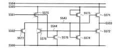
図15に示す信号線駆動回路は、ドライバIC5601、スイッチ群5602_1〜56
02_M、第1の配線5611、第2の配線5612、第3の配線5613及び配線56
21_1〜5621_Mを有する。スイッチ群5602_1〜5602_Mそれぞれは、
第1の薄膜トランジスタ5603a、第2の薄膜トランジスタ5603b及び第3の薄膜
トランジスタ5603cを有する。A signal line driver circuit illustrated in FIG. 15 includes a
02_M, the first wiring 5611, the
21_1 to 5621_M. Each of the switch groups 5602_1 to 5602_M
A first
ドライバIC5601は第1の配線5611、第2の配線5612、第3の配線5613
及び配線5621_1〜5621_Mに接続される。そして、スイッチ群5602_1〜
5602_Mそれぞれは、第1の配線5611、第2の配線5612、第3の配線561
3及びスイッチ群5602_1〜5602_Mそれぞれに対応した配線5621_1〜5
621_Mに接続される。そして、配線5621_1〜5621_Mそれぞれは、第1の
薄膜トランジスタ5603a、第2の薄膜トランジスタ5603b及び第3の薄膜トラン
ジスタ5603cを介して、3つの信号線に接続される。例えば、J列目の配線5621
_J(配線5621_1〜配線5621_Mのうちいずれか一)は、スイッチ群5602
_Jが有する第1の薄膜トランジスタ5603a、第2の薄膜トランジスタ5603b及
び第3の薄膜トランジスタ5603cを介して、信号線Sj−1、信号線Sj、信号線S
j+1に接続される。The
And the wirings 5621_1 to 5621_M. And switch group 5602_1-
Each of 5602_M includes a first wiring 5611, a
3 and switches 5621_1 to 5602_1 to 5602_1 to 5602_M respectively.
621_M. Each of the wirings 5621_1 to 5621_M is connected to three signal lines through the first
_J (any one of the wirings 5621_1 to 5621_M) is a switch group 5602.
_J includes the signal line Sj-1, the signal line Sj, and the signal line S through the first
connected to j + 1.
なお、第1の配線5611、第2の配線5612、第3の配線5613には、それぞれ信
号が入力される。Note that a signal is input to each of the first wiring 5611, the
なお、ドライバIC5601は、単結晶基板上に形成されていることが望ましい。さらに
、スイッチ群5602_1〜5602_Mは、画素部と同一基板上に形成されていること
が望ましい。したがって、ドライバIC5601とスイッチ群5602_1〜5602_
MとはFPCなどを介して接続するとよい。Note that the
It is good to connect with M through FPC or the like.
次に、図15に示した信号線駆動回路の動作について、図16のタイミングチャートを参
照して説明する。なお、図16のタイミングチャートは、i行目の走査線Giが選択され
ている場合のタイミングチャートを示している。さらに、i行目の走査線Giの選択期間
は、第1のサブ選択期間T1、第2のサブ選択期間T2及び第3のサブ選択期間T3に分
割されている。さらに、図15の信号線駆動回路は、他の行の走査線が選択されている場
合でも図16と同様の動作をする。Next, operation of the signal line driver circuit illustrated in FIG. 15 is described with reference to a timing chart of FIG. Note that the timing chart of FIG. 16 shows the timing chart when the i-th scanning line Gi is selected. Further, the selection period of the i-th scanning line Gi is divided into a first sub-selection period T1, a second sub-selection period T2, and a third sub-selection period T3. Further, the signal line driver circuit in FIG. 15 operates in the same manner as in FIG. 16 even when a scan line in another row is selected.
なお、図16のタイミングチャートは、J列目の配線5621_Jが第1の薄膜トランジ
スタ5603a、第2の薄膜トランジスタ5603b及び第3の薄膜トランジスタ560
3cを介して、信号線Sj−1、信号線Sj、信号線Sj+1に接続される場合について
示している。Note that in the timing chart in FIG. 16, the wiring 5621_J in the J-th column includes the first
A case where the signal line Sj−1, the signal line Sj, and the signal line Sj + 1 are connected via 3c is illustrated.
なお、図16のタイミングチャートは、i行目の走査線Giが選択されるタイミング、第
1の薄膜トランジスタ5603aのオン・オフのタイミング5703a、第2の薄膜トラ
ンジスタ5603bのオン・オフのタイミング5703b、第3の薄膜トランジスタ56
03cのオン・オフのタイミング5703c及びJ列目の配線5621_Jに入力される
信号5721_Jを示している。Note that in the timing chart of FIG. 16, the timing at which the i-th scanning line Gi is selected, the on / off timing 5703a of the first
In addition, an ON / OFF timing 5703c of 03c and a signal 5721_J input to the wiring 5621_J in the J-th column are illustrated.
なお、配線5621_1〜配線5621_Mには第1のサブ選択期間T1、第2のサブ選
択期間T2及び第3のサブ選択期間T3において、それぞれ別のビデオ信号が入力される
。例えば、第1のサブ選択期間T1において配線5621_Jに入力されるビデオ信号は
信号線Sj−1に入力され、第2のサブ選択期間T2において配線5621_Jに入力さ
れるビデオ信号は信号線Sjに入力され、第3のサブ選択期間T3において配線5621
_Jに入力されるビデオ信号は信号線Sj+1に入力される。さらに、第1のサブ選択期
間T1、第2のサブ選択期間T2及び第3のサブ選択期間T3において、配線5621_
Jに入力されるビデオ信号をそれぞれData_j−1、Data_j、Data_j+
1とする。Note that different video signals are input to the wirings 5621_1 to 5621_M in the first sub-selection period T1, the second sub-selection period T2, and the third sub-selection period T3. For example, a video signal input to the wiring 5621_J in the first sub-selection period T1 is input to the signal line Sj-1, and a video signal input to the wiring 5621_J in the second sub-selection period T2 is input to the signal line Sj. In the third sub-selection period T3, the wiring 5621
The video signal input to _J is input to the signal
The video signals input to J are represented by Data_j-1, Data_j, Data_j +, respectively.
Set to 1.
図16に示すように、第1のサブ選択期間T1において第1の薄膜トランジスタ5603
aがオンし、第2の薄膜トランジスタ5603b及び第3の薄膜トランジスタ5603c
がオフする。このとき、配線5621_Jに入力されるData_j−1が、第1の薄膜
トランジスタ5603aを介して信号線Sj−1に入力される。第2のサブ選択期間T2
では、第2の薄膜トランジスタ5603bがオンし、第1の薄膜トランジスタ5603a
及び第3の薄膜トランジスタ5603cがオフする。このとき、配線5621_Jに入力
されるData_jが、第2の薄膜トランジスタ5603bを介して信号線Sjに入力さ
れる。第3のサブ選択期間T3では、第3の薄膜トランジスタ5603cがオンし、第1
の薄膜トランジスタ5603a及び第2の薄膜トランジスタ5603bがオフする。この
とき、配線5621_Jに入力されるData_j+1が、第3の薄膜トランジスタ56
03cを介して信号線Sj+1に入力される。As shown in FIG. 16, in the first sub-selection period T1, the first thin film transistor 5603 is used.
a turns on, the second
Turns off. At this time, Data_j−1 input to the wiring 5621_J is input to the signal line Sj−1 through the first
Then, the second
Then, the third
The
The signal is input to the signal line Sj + 1 via 03c.
以上のことから、図15の信号線駆動回路は、1ゲート選択期間を3つに分割することで
、1ゲート選択期間中に1つの配線5621から3つの信号線にビデオ信号を入力するこ
とができる。したがって、図15の信号線駆動回路は、ドライバIC5601が形成され
る基板と、画素部が形成されている基板との接続数を信号線の数に比べて約1/3にする
ことができる。接続数が約1/3になることによって、図15の信号線駆動回路は、信頼
性、歩留まりなどを向上できる。From the above, the signal line driver circuit in FIG. 15 can input a video signal from one wiring 5621 to three signal lines during one gate selection period by dividing one gate selection period into three. it can. Therefore, the signal line driver circuit in FIG. 15 can reduce the number of connections between the substrate on which the
なお、図15のように、1ゲート選択期間を複数のサブ選択期間に分割し、複数のサブ選
択期間それぞれにおいて、ある1つの配線から複数の信号線それぞれにビデオ信号を入力
することができれば、薄膜トランジスタの配置や数、駆動方法などは限定されない。As shown in FIG. 15, if one gate selection period is divided into a plurality of sub-selection periods and a video signal can be input from a certain wiring to each of a plurality of signal lines in each of the plurality of sub-selection periods, The arrangement and number of thin film transistors and the driving method are not limited.
例えば、3つ以上のサブ選択期間それぞれにおいて1つの配線から3つ以上の信号線それ
ぞれにビデオ信号を入力する場合は、薄膜トランジスタ及び薄膜トランジスタを制御する
ための配線を追加すればよい。ただし、1ゲート選択期間を4つ以上のサブ選択期間に分
割すると、1つのサブ選択期間が短くなる。したがって、1ゲート選択期間は、2つ又は
3つのサブ選択期間に分割されることが望ましい。For example, when video signals are input from one wiring to each of three or more signal lines in each of three or more sub-selection periods, a thin film transistor and a wiring for controlling the thin film transistor may be added. However, if one gate selection period is divided into four or more sub selection periods, one sub selection period is shortened. Therefore, it is desirable that one gate selection period is divided into two or three sub selection periods.
別の例として、図17のタイミングチャートに示すように、1つの選択期間をプリチャー
ジ期間Tp、第1のサブ選択期間T1、第2のサブ選択期間T2、第3の選択期間T3に
分割してもよい。さらに、図17のタイミングチャートは、i行目の走査線Giが選択さ
れるタイミング、第1の薄膜トランジスタ5603aのオン・オフのタイミング5803
a、第2の薄膜トランジスタ5603bのオン・オフのタイミング5803b、第3の薄
膜トランジスタ5603cのオン・オフのタイミング5803c及びJ列目の配線562
1_Jに入力される信号5821_Jを示している。図17に示すように、プリチャージ
期間Tpにおいて第1の薄膜トランジスタ5603a、第2の薄膜トランジスタ5603
b及び第3の薄膜トランジスタ5603cがオンする。このとき、配線5621_Jに入
力されるプリチャージ電圧Vpが第1の薄膜トランジスタ5603a、第2の薄膜トラン
ジスタ5603b及び第3の薄膜トランジスタ5603cを介してそれぞれ信号線Sj−
1、信号線Sj、信号線Sj+1に入力される。第1のサブ選択期間T1において第1の
薄膜トランジスタ5603aがオンし、第2の薄膜トランジスタ5603b及び第3の薄
膜トランジスタ5603cがオフする。このとき、配線5621_Jに入力されるDat
a_j−1が、第1の薄膜トランジスタ5603aを介して信号線Sj−1に入力される
。第2のサブ選択期間T2では、第2の薄膜トランジスタ5603bがオンし、第1の薄
膜トランジスタ5603a及び第3の薄膜トランジスタ5603cがオフする。このとき
、配線5621_Jに入力されるData_jが、第2の薄膜トランジスタ5603bを
介して信号線Sjに入力される。第3のサブ選択期間T3では、第3の薄膜トランジスタ
5603cがオンし、第1の薄膜トランジスタ5603a及び第2の薄膜トランジスタ5
603bがオフする。このとき、配線5621_Jに入力されるData_j+1が、第
3の薄膜トランジスタ5603cを介して信号線Sj+1に入力される。As another example, as shown in the timing chart of FIG. 17, one selection period is divided into a precharge period Tp, a first sub selection period T1, a second sub selection period T2, and a third selection period T3. May be. Further, in the timing chart of FIG. 17, the timing at which the i-th scanning line Gi is selected, the on-off timing 5803 of the first
a, ON /
The signal 5821_J input to 1_J is shown. As shown in FIG. 17, in the precharge period Tp, the first
b and the third
1 is input to the signal line Sj and the signal
a_j−1 is input to the signal line Sj−1 through the first
603b is turned off. At this time, Data_j + 1 input to the wiring 5621_J is input to the signal line Sj + 1 through the third
以上のことから、図17のタイミングチャートを適用した図15の信号線駆動回路は、サ
ブ選択期間の前にプリチャージ選択期間を設けることによって、信号線をプリチャージで
きるため、画素へのビデオ信号の書き込みを高速に行うことができる。なお、図17にお
いて、図16と同様なものに関しては共通の符号を用いて示し、同一部分又は同様な機能
を有する部分の詳細な説明は省略する。From the above, the signal line driver circuit in FIG. 15 to which the timing chart in FIG. 17 is applied can precharge the signal line by providing the precharge selection period before the sub selection period. Can be written at high speed. Note that in FIG. 17, components similar to those in FIG. 16 are denoted by common reference numerals, and detailed description of the same portions or portions having similar functions is omitted.
また、走査線駆動回路の構成について説明する。走査線駆動回路は、シフトレジスタ、バ
ッファを有している。また場合によってはレベルシフタを有していても良い。走査線駆動
回路において、シフトレジスタにクロック信号(CLK)及びスタートパルス信号(SP
)が入力されることによって、選択信号が生成される。生成された選択信号はバッファに
おいて緩衝増幅され、対応する走査線に供給される。走査線には、1ライン分の画素のト
ランジスタのゲート電極が接続されている。そして、1ライン分の画素のトランジスタを
一斉にONにしなくてはならないので、バッファは大きな電流を流すことが可能なものが
用いられる。A structure of the scan line driver circuit will be described. The scan line driver circuit includes a shift register and a buffer. In some cases, a level shifter may be provided. In the scan line driver circuit, a clock signal (CLK) and a start pulse signal (SP
) Is input, a selection signal is generated. The generated selection signal is buffered and amplified in the buffer and supplied to the corresponding scanning line. A gate electrode of a transistor of a pixel for one line is connected to the scanning line. Since the transistors of pixels for one line must be turned on all at once, a buffer that can flow a large current is used.
走査線駆動回路の一部に用いるシフトレジスタの一形態について図18及び図19を用い
て説明する。One mode of a shift register used for part of the scan line driver circuit is described with reference to FIGS.
図18にシフトレジスタの回路構成を示す。図18に示すシフトレジスタは、フリップフ
ロップ5701_1〜5701_nという複数のフリップフロップで構成される。また、
第1のクロック信号、第2のクロック信号、スタートパルス信号、リセット信号が入力さ
れて動作する。FIG. 18 shows a circuit configuration of the shift register. The shift register illustrated in FIG. 18 includes a plurality of flip-flops, flip-flops 5701_1 to 5701_n. Also,
The first clock signal, the second clock signal, the start pulse signal, and the reset signal are input to operate.
図18のシフトレジスタの接続関係について説明する。図18のシフトレジスタは、i段
目のフリップフロップ5701_i(フリップフロップ5701_1〜5701_nのう
ちいずれか一)は、図19に示した第1の配線5501が第7の配線5717_i−1に
接続され、図19に示した第2の配線5502が第7の配線5717_i+1に接続され
、図19に示した第3の配線5503が第7の配線5717_iに接続され、図19に示
した第6の配線5506が第5の配線5715に接続される。Connection relations of the shift register in FIG. 18 are described. In the shift register in FIG. 18, the i-th flip-flop 5701_i (any one of the flip-flops 5701_1 to 5701_n) has the
また、図19に示した第4の配線5504が奇数段目のフリップフロップでは第2の配線
5712に接続され、偶数段目のフリップフロップでは第3の配線5713に接続され、
図19に示した第5の配線5505が第4の配線5714に接続される。19 is connected to the
The
ただし、1段目のフリップフロップ5701_1の図19に示す第1の配線5501は第
1の配線5711に接続され、n段目のフリップフロップ5701_nの図19に示す第
2の配線5502は第6の配線5716に接続される。Note that the
なお、第1の配線5711、第2の配線5712、第3の配線5713、第6の配線57
16を、それぞれ第1の信号線、第2の信号線、第3の信号線、第4の信号線と呼んでも
よい。さらに、第4の配線5714、第5の配線5715を、それぞれ第1の電源線、第
2の電源線と呼んでもよい。Note that the
16 may be referred to as a first signal line, a second signal line, a third signal line, and a fourth signal line, respectively. Further, the
次に、図18に示すフリップフロップの詳細について、図19に示す。図19に示すフリ
ップフロップは、第1の薄膜トランジスタ5571、第2の薄膜トランジスタ5572、
第3の薄膜トランジスタ5573、第4の薄膜トランジスタ5574、第5の薄膜トラン
ジスタ5575、第6の薄膜トランジスタ5576、第7の薄膜トランジスタ5577及
び第8の薄膜トランジスタ5578を有する。なお、第1の薄膜トランジスタ5571、
第2の薄膜トランジスタ5572、第3の薄膜トランジスタ5573、第4の薄膜トラン
ジスタ5574、第5の薄膜トランジスタ5575、第6の薄膜トランジスタ5576、
第7の薄膜トランジスタ5577及び第8の薄膜トランジスタ5578は、nチャネル型
トランジスタであり、ゲート・ソース間電圧(Vgs)がしきい値電圧(Vth)を上回
ったとき導通状態になるものとする。Next, FIG. 19 shows details of the flip-flop shown in FIG. A flip-flop illustrated in FIG. 19 includes a first
A third
The second
The seventh
次に、図18に示すフリップフロップの接続構成について、以下に示す。Next, a connection structure of the flip-flop illustrated in FIG. 18 is described below.
第1の薄膜トランジスタ5571の第1の電極(ソース電極またはドレイン電極の一方)
が第4の配線5504に接続され、第1の薄膜トランジスタ5571の第2の電極(ソー
ス電極またはドレイン電極の他方)が第3の配線5503に接続される。First electrode of the first thin film transistor 5571 (one of a source electrode and a drain electrode)
Is connected to the
第2の薄膜トランジスタ5572の第1の電極が第6の配線5506に接続され、第2の
薄膜トランジスタ5572第2の電極が第3の配線5503に接続される。A first electrode of the second
第3の薄膜トランジスタ5573の第1の電極が第5の配線5505に接続され、第3の
薄膜トランジスタ5573の第2の電極が第2の薄膜トランジスタ5572のゲート電極
に接続され、第3の薄膜トランジスタ5573のゲート電極が第5の配線5505に接続
される。The first electrode of the third
第4の薄膜トランジスタ5574の第1の電極が第6の配線5506に接続され、第4の
薄膜トランジスタ5574の第2の電極が第2の薄膜トランジスタ5572のゲート電極
に接続され、第4の薄膜トランジスタ5574のゲート電極が第1の薄膜トランジスタ5
571のゲート電極に接続される。The first electrode of the fourth
571 is connected to the gate electrode.
第5の薄膜トランジスタ5575の第1の電極が第5の配線5505に接続され、第5の
薄膜トランジスタ5575の第2の電極が第1の薄膜トランジスタ5571のゲート電極
に接続され、第5の薄膜トランジスタ5575のゲート電極が第1の配線5501に接続
される。The first electrode of the fifth
第6の薄膜トランジスタ5576の第1の電極が第6の配線5506に接続され、第6の
薄膜トランジスタ5576の第2の電極が第1の薄膜トランジスタ5571のゲート電極
に接続され、第6の薄膜トランジスタ5576のゲート電極が第2の薄膜トランジスタ5
572のゲート電極に接続される。The first electrode of the sixth
572 is connected to the gate electrode.
第7の薄膜トランジスタ5577の第1の電極が第6の配線5506に接続され、第7の
薄膜トランジスタ5577の第2の電極が第1の薄膜トランジスタ5571のゲート電極
に接続され、第7の薄膜トランジスタ5577のゲート電極が第2の配線5502に接続
される。第8の薄膜トランジスタ5578の第1の電極が第6の配線5506に接続され
、第8の薄膜トランジスタ5578の第2の電極が第2の薄膜トランジスタ5572のゲ
ート電極に接続され、第8の薄膜トランジスタ5578のゲート電極が第1の配線550
1に接続される。The first electrode of the seventh
1 is connected.
なお、第1の薄膜トランジスタ5571のゲート電極、第4の薄膜トランジスタ5574
のゲート電極、第5の薄膜トランジスタ5575の第2の電極、第6の薄膜トランジスタ
5576の第2の電極及び第7の薄膜トランジスタ5577の第2の電極の接続箇所をノ
ード5543とする。さらに、第2の薄膜トランジスタ5572のゲート電極、第3の薄
膜トランジスタ5573の第2の電極、第4の薄膜トランジスタ5574の第2の電極、
第6の薄膜トランジスタ5576のゲート電極及び第8の薄膜トランジスタ5578の第
2の電極の接続箇所をノード5544とする。Note that the gate electrode of the first
A connection position of the second electrode of the fifth
A connection position between the gate electrode of the sixth
なお、第1の配線5501、第2の配線5502、第3の配線5503及び第4の配線5
504を、それぞれ第1の信号線、第2の信号線、第3の信号線、第4の信号線と呼んで
もよい。さらに、第5の配線5505を第1の電源線、第6の配線5506を第2の電源
線と呼んでもよい。Note that the
504 may be referred to as a first signal line, a second signal line, a third signal line, and a fourth signal line, respectively. Further, the
また、信号線駆動回路及び走査線駆動回路を実施の形態1乃至3に示すnチャネル型TF
Tのみで作製することも可能である。実施の形態1乃至3に示すnチャネル型TFTはト
ランジスタの移動度が大きいため、駆動回路の駆動周波数を高くすることが可能となる。
また、実施の形態1乃至3に示すnチャネル型TFTは寄生容量が低減されるため、周波
数特性(f特性と呼ばれる)が高い。例えば、実施の形態1乃至3に示すnチャネル型T
FTを用いた走査線駆動回路は、高速に動作させることができるため、フレーム周波数を
高くすること、または、黒画面挿入を実現することなども実現することができる。Further, the signal line driver circuit and the scan line driver circuit are n-channel TFs shown in
It is also possible to produce only with T. Since the n-channel TFTs described in
In addition, the n-channel TFT described in any of
Since the scanning line driving circuit using FT can be operated at high speed, it is possible to increase the frame frequency or to realize black screen insertion.
さらに、走査線駆動回路のトランジスタのチャネル幅を大きくすることや、複数の走査線
駆動回路を配置することなどによって、さらに高いフレーム周波数を実現することができ
る。複数の走査線駆動回路を配置する場合は、偶数行の走査線を駆動する為の走査線駆動
回路を片側に配置し、奇数行の走査線を駆動するための走査線駆動回路をその反対側に配
置することにより、フレーム周波数を高くすることを実現することができる。また、複数
の走査線駆動回路により、同じ走査線に信号を出力すると、表示装置の大型化に有利であ
る。Further, a higher frame frequency can be realized by increasing the channel width of the transistor in the scan line driver circuit or disposing a plurality of scan line driver circuits. When a plurality of scanning line driving circuits are arranged, a scanning line driving circuit for driving even-numbered scanning lines is arranged on one side, and a scanning line driving circuit for driving odd-numbered scanning lines is arranged on the opposite side. By arranging them in this manner, it is possible to increase the frame frequency. In addition, when a plurality of scanning line driving circuits outputs signals to the same scanning line, it is advantageous for increasing the size of the display device.
また、半導体装置の一例であるアクティブマトリクス型発光表示装置を作製する場合、少
なくとも一つの画素に複数の薄膜トランジスタを配置するため、走査線駆動回路を複数配
置することが好ましい。アクティブマトリクス型発光表示装置のブロック図の一例を図1
4(B)に示す。In the case of manufacturing an active matrix light-emitting display device which is an example of a semiconductor device, it is preferable to provide a plurality of scan line driver circuits in order to arrange a plurality of thin film transistors in at least one pixel. An example of a block diagram of an active matrix light-emitting display device is shown in FIG.
Shown in 4 (B).
図14(B)に示す発光表示装置は、基板5400上に表示素子を備えた画素を複数有す
る画素部5401と、各画素を選択する第1の走査線駆動回路5402及び第2の走査線
駆動回路5404と、選択された画素へのビデオ信号の入力を制御する信号線駆動回路5
403とを有する。A light-emitting display device illustrated in FIG. 14B includes a pixel portion 5401 having a plurality of pixels each provided with a display element over a
403.
図14(B)に示す発光表示装置の画素に入力されるビデオ信号をデジタル形式とする場
合、画素はトランジスタのオンとオフの切り替えによって、発光もしくは非発光の状態と
なる。よって、面積階調法または時間階調法を用いて階調の表示を行うことができる。面
積階調法は、1画素を複数の副画素に分割し、各副画素を独立にビデオ信号に基づいて駆
動させることによって、階調表示を行う駆動法である。また時間階調法は、画素が発光す
る期間を制御することによって、階調表示を行う駆動法である。In the case where a video signal input to the pixel of the light-emitting display device illustrated in FIG. 14B is in a digital format, the pixel is turned on or off by switching on and off of the transistor. Therefore, gradation display can be performed using the area gradation method or the time gradation method. The area gradation method is a driving method in which gradation display is performed by dividing one pixel into a plurality of subpixels and independently driving each subpixel based on a video signal. The time gray scale method is a driving method for performing gray scale display by controlling a period during which a pixel emits light.
発光素子は、液晶素子などに比べて応答速度が高いので、液晶素子よりも時間階調法に適
している。具体的に時間階調法で表示を行なう場合、1フレーム期間を複数のサブフレー
ム期間に分割する。そしてビデオ信号に従い、各サブフレーム期間において画素の発光素
子を発光または非発光の状態にする。複数のサブフレーム期間に分割することによって、
1フレーム期間中に画素が実際に発光する期間のトータルの長さを、ビデオ信号により制
御することができ、階調を表示することができる。Since a light emitting element has a higher response speed than a liquid crystal element or the like, it is more suitable for a time gray scale method than a liquid crystal element. Specifically, when displaying by the time gray scale method, one frame period is divided into a plurality of subframe periods. Then, in accordance with the video signal, the light emitting element of the pixel is turned on or off in each subframe period. By dividing into multiple subframe periods,
The total length of a period during which a pixel actually emits light during one frame period can be controlled by a video signal, so that gradation can be displayed.
なお、図14(B)に示す発光表示装置では、一つの画素に2つのスイッチング用TFT
を配置する場合、一方のスイッチング用TFTのゲート配線である第1の走査線に入力さ
れる信号を第1走査線駆動回路5402で生成し、他方のスイッチング用TFTのゲート
配線である第2の走査線に入力される信号を第2の走査線駆動回路5404で生成してい
る例を示しているが、第1の走査線に入力される信号と、第2の走査線に入力される信号
とを、共に1つの走査線駆動回路で生成するようにしても良い。また、例えば、1つの画
素が有するスイッチング用TFTの数によって、スイッチング素子の動作を制御するのに
用いられる走査線が、各画素に複数設けられることもあり得る。この場合、複数の走査線
に入力される信号を、全て1つの走査線駆動回路で生成しても良いし、複数の各走査線駆
動回路で生成しても良い。Note that in the light-emitting display device illustrated in FIG. 14B, two switching TFTs are included in one pixel.
, A signal input to the first scanning line which is the gate wiring of one switching TFT is generated by the first scanning
また、発光表示装置においても、駆動回路のうち、nチャネル型TFTで構成することが
できる駆動回路の一部を画素部の薄膜トランジスタと同一基板上に形成することができる
。また、信号線駆動回路及び走査線駆動回路を実施の形態1乃至3に示すnチャネル型T
FTのみで作製することも可能である。In the light-emitting display device, part of a driver circuit that can include n-channel TFTs among driver circuits can be formed over the same substrate as the thin film transistor in the pixel portion. In addition, the signal line driver circuit and the scan line driver circuit are formed using the n-channel T shown in
It is also possible to produce only by FT.
また、上述した駆動回路は、液晶表示装置や発光表示装置に限らず、スイッチング素子と
電気的に接続する素子を利用して電子インクを駆動させる電子ペーパーに用いてもよい。
電子ペーパーは、電気泳動表示装置(電気泳動ディスプレイ)も呼ばれており、紙と同じ
読みやすさ、他の表示装置に比べ低消費電力、薄くて軽い形状とすることが可能という利
点を有している。The driving circuit described above is not limited to a liquid crystal display device or a light-emitting display device, and may be used for electronic paper that drives electronic ink using an element that is electrically connected to a switching element.
Electronic paper is also called an electrophoretic display device (electrophoretic display), and has the same readability as paper, low power consumption compared to other display devices, and the advantage of being thin and light. ing.
電気泳動ディスプレイは、様々な形態が考えられ得るが、プラスの電荷を有する第1の粒
子と、マイナスの電荷を有する第2の粒子とを含むマイクロカプセルが溶媒または溶質に
複数分散されたものであり、マイクロカプセルに電界を印加することによって、マイクロ
カプセル中の粒子を互いに反対方向に移動させて一方側に集合した粒子の色のみを表示す
るものである。なお、第1の粒子または第2の粒子は染料を含み、電界がない場合におい
て移動しないものである。また、第1の粒子の色と第2の粒子の色は異なるもの(無色を
含む)とする。The electrophoretic display can be considered in various forms, and a plurality of microcapsules including first particles having a positive charge and second particles having a negative charge are dispersed in a solvent or a solute. In other words, by applying an electric field to the microcapsules, the particles in the microcapsules are moved in opposite directions to display only the color of the particles assembled on one side. Note that the first particle or the second particle contains a dye and does not move in the absence of an electric field. In addition, the color of the first particles and the color of the second particles are different (including colorless).
このように、電気泳動ディスプレイは、誘電定数の高い物質が高い電界領域に移動する、
いわゆる誘電泳動的効果を利用したディスプレイである。電気泳動ディスプレイは、液晶
表示装置に必要な偏光板が必要ない。In this way, the electrophoretic display moves a substance having a high dielectric constant to a high electric field region.
This is a display using the so-called dielectrophoretic effect. The electrophoretic display does not require a polarizing plate necessary for a liquid crystal display device.
上記マイクロカプセルを溶媒中に分散させたものが電子インクと呼ばれるものであり、こ
の電子インクはガラス、プラスチック、布、紙などの表面に印刷することができる。また
、カラーフィルタや色素を有する粒子を用いることによってカラー表示も可能である。A solution in which the above microcapsules are dispersed in a solvent is referred to as electronic ink. This electronic ink can be printed on a surface of glass, plastic, cloth, paper, or the like. Color display is also possible by using particles having color filters or pigments.
また、アクティブマトリクス基板上に適宜、二つの電極の間に挟まれるように上記マイク
ロカプセルを複数配置すればアクティブマトリクス型の表示装置が完成し、マイクロカプ
セルに電界を印加すれば表示を行うことができる。例えば、実施の形態1乃至3の薄膜ト
ランジスタによって得られるアクティブマトリクス基板を用いることができる。In addition, an active matrix display device can be completed by arranging a plurality of the above microcapsules so as to be appropriately sandwiched between two electrodes on an active matrix substrate, and display can be performed by applying an electric field to the microcapsules. it can. For example, the active matrix substrate obtained by the thin film transistor of
なお、マイクロカプセル中の第1の粒子および第2の粒子は、導電体材料、絶縁体材料、
半導体材料、磁性材料、液晶材料、強誘電性材料、エレクトロルミネセント材料、エレク
トロクロミック材料、磁気泳動材料から選ばれた一種の材料、またはこれらの複合材料を
用いればよい。Note that the first particle and the second particle in the microcapsule are a conductor material, an insulator material,
A material selected from semiconductor materials, magnetic materials, liquid crystal materials, ferroelectric materials, electroluminescent materials, electrochromic materials, and magnetophoretic materials, or a composite material thereof may be used.
以上の工程により、半導体装置として信頼性の高い表示装置を作製することができる。Through the above process, a highly reliable display device as a semiconductor device can be manufactured.
本実施の形態は、他の実施の形態に記載した構成と適宜組み合わせて実施することが可能
である。This embodiment can be implemented in appropriate combination with the structures described in the other embodiments.
(実施の形態5)
薄膜トランジスタを作製し、該薄膜トランジスタを画素部、さらには駆動回路に用いて表
示機能を有する半導体装置(表示装置ともいう)を作製することができる。また、薄膜ト
ランジスタを駆動回路の一部または全体を、画素部と同じ基板上に一体形成し、システム
オンパネルを形成することができる。(Embodiment 5)
A thin film transistor is manufactured, and a semiconductor device having a display function (also referred to as a display device) can be manufactured using the thin film transistor in a pixel portion and further in a driver circuit. In addition, a part of or the entire driving circuit of the thin film transistor can be formed over the same substrate as the pixel portion to form a system-on-panel.
表示装置は表示素子を含む。表示素子としては液晶素子(液晶表示素子ともいう)、発光
素子(発光表示素子ともいう)を用いることができる。発光素子は、電流または電圧によ
って輝度が制御される素子をその範疇に含んでおり、具体的には無機EL(Electr
o Luminescence)、有機EL等が含まれる。また、電子インクなど、電気
的作用によりコントラストが変化する表示媒体も適用することができる。The display device includes a display element. As the display element, a liquid crystal element (also referred to as a liquid crystal display element) or a light-emitting element (also referred to as a light-emitting display element) can be used. A light-emitting element includes an element whose luminance is controlled by current or voltage, specifically, an inorganic EL (Electr EL).
o Luminescence), organic EL, and the like. In addition, a display medium whose contrast is changed by an electric effect, such as electronic ink, can be used.
また、表示装置は、表示素子が封止された状態にあるパネルと、該パネルにコントローラ
を含むIC等を実装した状態にあるモジュールとを含む。さらに、該表示装置を作製する
過程における、表示素子が完成する前の一形態に相当する素子基板に関し、該素子基板は
、電流を表示素子に供給するための手段を複数の各画素に備える。素子基板は、具体的に
は、表示素子の画素電極のみが形成された状態であっても良いし、画素電極となる導電膜
を成膜した後であって、エッチングして画素電極を形成する前の状態であっても良いし、
あらゆる形態があてはまる。The display device includes a panel in which the display element is sealed, and a module in which an IC including a controller is mounted on the panel. Further, in the process of manufacturing the display device, the element substrate which corresponds to one embodiment before the display element is completed is provided with a means for supplying current to the display element in each of the plurality of pixels. Specifically, the element substrate may be in a state where only the pixel electrode of the display element is formed, or after the conductive film to be the pixel electrode is formed, the pixel electrode is formed by etching. It may be in the previous state,
All forms apply.
なお、本明細書中における表示装置とは、画像表示デバイス、表示デバイス、もしくは光
源(照明装置含む)を指す。また、コネクター、例えばFPC(Flexible pr
inted circuit)もしくはTAB(Tape Automated Bon
ding)テープもしくはTCP(Tape Carrier Package)が取り
付けられたモジュール、TABテープやTCPの先にプリント配線板が設けられたモジュ
ール、または表示素子にCOG(Chip On Glass)方式によりIC(集積回
路)が直接実装されたモジュールも全て表示装置に含むものとする。Note that a display device in this specification means an image display device, a display device, or a light source (including a lighting device). Also, a connector such as an FPC (Flexible pr
integrated circuit) or TAB (Tape Automated Bon)
ding) tape or TCP (Tape Carrier Package) attached module, TAB tape or TCP is provided with a printed wiring board, or a display element is an IC (integrated circuit) by COG (Chip On Glass) method. All directly mounted modules are included in the display device.
半導体装置の一形態に相当する液晶表示パネルの外観及び断面について、図10を用いて
説明する。図10は、第1の基板4001上に形成された実施の形態3で示した酸化物半
導体層を含む信頼性の高い薄膜トランジスタ4010、4011、及び液晶素子4013
を、第2の基板4006との間にシール材4005によって封止した、パネルの平面図で
あり、図10(B)は、図10(A1)(A2)のM−Nにおける断面図に相当する。An appearance and a cross section of a liquid crystal display panel, which is one embodiment of a semiconductor device, will be described with reference to FIGS. FIG. 10 shows highly reliable
FIG. 10B is a plan view of the panel sealed with the
第1の基板4001上に設けられた画素部4002と、走査線駆動回路4004とを囲む
ようにして、シール材4005が設けられている。また画素部4002と、走査線駆動回
路4004の上に第2の基板4006が設けられている。よって画素部4002と、走査
線駆動回路4004とは、第1の基板4001とシール材4005と第2の基板4006
とによって、液晶層4008と共に封止されている。また第1の基板4001上のシール
材4005によって囲まれている領域とは異なる領域に、別途用意された基板上に単結晶
半導体膜又は多結晶半導体膜で形成された信号線駆動回路4003が実装されている。A
Are sealed together with the
なお、別途形成した駆動回路の接続方法は、特に限定されるものではなく、COG方法、
ワイヤボンディング方法、或いはTAB方法などを用いることができる。図10(A1)
は、COG方法により信号線駆動回路4003を実装する例であり、図10(A2)は、
TAB方法により信号線駆動回路4003を実装する例である。Note that a connection method of a separately formed drive circuit is not particularly limited, and a COG method,
A wire bonding method, a TAB method, or the like can be used. FIG. 10 (A1)
Is an example in which the signal
In this example, the signal
また第1の基板4001上に設けられた画素部4002と、走査線駆動回路4004は、
薄膜トランジスタを複数有しており、図10(B)では、画素部4002に含まれる薄膜
トランジスタ4010と、走査線駆動回路4004に含まれる薄膜トランジスタ4011
とを例示している。薄膜トランジスタ4010、4011上には絶縁層4020、402
1が設けられている。In addition, the
10B, the
And are illustrated. Insulating
1 is provided.
薄膜トランジスタ4010、4011は、実施の形態3で示した酸化物半導体層を含む信
頼性の高い薄膜トランジスタを適用することができる。また実施の形態1又は実施の形態
2に示す薄膜トランジスタを適用してもよい。本実施の形態において、薄膜トランジスタ
4010、4011はnチャネル型薄膜トランジスタである。As the
また、液晶素子4013が有する画素電極層4030は、薄膜トランジスタ4010と電
気的に接続されている。そして液晶素子4013の対向電極層4031は第2の基板40
06上に形成されている。画素電極層4030と対向電極層4031と液晶層4008と
が重なっている部分が、液晶素子4013に相当する。なお、画素電極層4030、対向
電極層4031はそれぞれ配向膜として機能する絶縁層4032、4033が設けられ、
絶縁層4032、4033を介して液晶層4008を挟持している。In addition, the
06 is formed. A portion where the
A
なお、第1の基板4001、第2の基板4006としては、ガラス、金属(代表的にはス
テンレス)、セラミックス、プラスチックを用いることができる。プラスチックとしては
、FRP(Fiberglass−Reinforced Plastics)板、PV
F(ポリビニルフルオライド)フィルム、ポリエステルフィルム、またはアクリル樹脂フ
ィルムを用いることができる。また、アルミニウムホイルをPVFフィルムやポリエステ
ルフィルムで挟んだ構造のシートを用いることもできる。Note that as the
An F (polyvinyl fluoride) film, a polyester film, or an acrylic resin film can be used. A sheet having a structure in which an aluminum foil is sandwiched between PVF films or polyester films can also be used.
また4035は絶縁膜を選択的にエッチングすることで得られる柱状のスペーサであり、
画素電極層4030と対向電極層4031との間の距離(セルギャップ)を制御するため
に設けられている。なお球状のスペーサを用いていても良い。また、対向電極層4031
は、薄膜トランジスタ4010と同一基板上に設けられる共通電位線と電気的に接続され
る。共通接続部を用いて、一対の基板間に配置される導電性粒子を介して対向電極層40
31と共通電位線とを電気的に接続することができる。なお、導電性粒子はシール材40
05に含有させる。4035 is a columnar spacer obtained by selectively etching the insulating film,
It is provided to control the distance (cell gap) between the
Are electrically connected to a common potential line provided over the same substrate as the
31 and the common potential line can be electrically connected. The conductive particles are the sealing
05.
また、配向膜を用いないブルー相を示す液晶を用いてもよい。ブルー相は液晶相の一つで
あり、コレステリック液晶を昇温していくと、コレステリック相から等方相へ転移する直
前に発現する相である。ブルー相は狭い温度範囲でしか発現しないため、温度範囲を改善
するために5重量%以上のカイラル剤を混合させた液晶組成物を用いて液晶層4008に
用いる。ブルー相を示す液晶とカイラル剤とを含む液晶組成物は、応答速度が1msec
以下と短く、光学的等方性であるため配向処理が不要であり、視野角依存性が小さい。Alternatively, a liquid crystal exhibiting a blue phase for which an alignment film is unnecessary may be used. The blue phase is one of the liquid crystal phases. When the temperature of the cholesteric liquid crystal is increased, the blue phase appears immediately before the transition from the cholesteric phase to the isotropic phase. Since the blue phase appears only in a narrow temperature range, a liquid crystal composition mixed with 5% by weight or more of a chiral agent is used for the
Since it is short as follows and is optically isotropic, alignment treatment is unnecessary, and viewing angle dependency is small.
なお透過型液晶表示装置の他に、反射型液晶表示装置でも半透過型液晶表示装置でも適用
できる。In addition to the transmissive liquid crystal display device, a reflective liquid crystal display device or a transflective liquid crystal display device can be applied.
また、液晶表示装置では、基板の外側(視認側)に偏光板を設け、内側に着色層、表示素
子に用いる電極層という順に設ける例を示すが、偏光板は基板の内側に設けてもよい。ま
た、偏光板と着色層の積層構造も本実施の形態に限定されず、偏光板及び着色層の材料や
作製工程条件によって適宜設定すればよい。また、ブラックマトリクスとして機能する遮
光膜を設けてもよい。In the liquid crystal display device, a polarizing plate is provided on the outer side (viewing side) of the substrate, a colored layer is provided on the inner side, and an electrode layer used for the display element is provided in this order, but the polarizing plate may be provided on the inner side of the substrate. . In addition, the stacked structure of the polarizing plate and the colored layer is not limited to this embodiment mode, and may be set as appropriate depending on the material and manufacturing process conditions of the polarizing plate and the colored layer. Further, a light shielding film functioning as a black matrix may be provided.
また、薄膜トランジスタの表面凹凸を低減するため、及び薄膜トランジスタの信頼性を向
上させるため、上記実施の形態で得られた薄膜トランジスタを保護膜や平坦化絶縁膜とし
て機能する絶縁層(絶縁層4020、絶縁層4021)で覆う構成となっている。なお、
保護膜は、大気中に浮遊する有機物や金属物、水蒸気などの汚染不純物の侵入を防ぐため
のものであり、緻密な膜が好ましい。保護膜は、スパッタ法を用いて、酸化珪素膜、窒化
珪素膜、酸化窒化珪素膜、窒化酸化珪素膜、酸化アルミニウム膜、窒化アルミニウム膜、
酸化窒化アルミニウム膜、又は窒化酸化アルミニウム膜の単層、又は積層で形成すればよ
い。保護膜をスパッタ法で形成する例を示すが、特に限定されず種々の方法で形成すれば
よい。In order to reduce surface roughness of the thin film transistor and improve the reliability of the thin film transistor, the thin film transistor obtained in the above embodiment functions as a protective film or a planarization insulating film (insulating
The protective film is for preventing entry of contaminant impurities such as organic substances, metal substances, and water vapor floating in the air, and a dense film is preferable. The protective film is formed by sputtering using a silicon oxide film, a silicon nitride film, a silicon oxynitride film, a silicon nitride oxide film, an aluminum oxide film, an aluminum nitride film,
An aluminum oxynitride film or an aluminum nitride oxide film may be formed as a single layer or a stacked layer. Although an example in which the protective film is formed by a sputtering method is shown, it is not particularly limited and may be formed by various methods.
ここでは、保護膜として積層構造の絶縁層4020を形成する。ここでは、絶縁層402
0の一層目として、スパッタ法を用いて酸化珪素膜を形成する。保護膜として酸化珪素膜
を用いると、ソース電極層及びドレイン電極層として用いるアルミニウム膜のヒロック防
止に効果がある。Here, an insulating
As the first layer, a silicon oxide film is formed by sputtering. The use of a silicon oxide film as the protective film is effective in preventing hillocks of the aluminum film used as the source electrode layer and the drain electrode layer.
また、保護膜の二層目として絶縁層を形成する。ここでは、絶縁層4020の二層目とし
て、スパッタ法を用いて窒化珪素膜を形成する。保護膜として窒化珪素膜を用いると、ナ
トリウム等の可動イオンが半導体領域中に侵入して、TFTの電気特性を変化させること
を抑制することができる。In addition, an insulating layer is formed as a second layer of the protective film. Here, as the second layer of the insulating
また、保護膜を形成した後に、窒素雰囲気下、又は大気雰囲気下で加熱処理(300℃以
下)を行ってもよい。Further, after the protective film is formed, heat treatment (300 ° C. or lower) may be performed in a nitrogen atmosphere or an air atmosphere.
また、平坦化絶縁膜として絶縁層4021を形成する。絶縁層4021としては、ポリイ
ミド、アクリル、ベンゾシクロブテン、ポリアミド、エポキシ等の、耐熱性を有する有機
材料を用いることができる。また上記有機材料の他に、低誘電率材料(low−k材料)
、シロキサン系樹脂、PSG(リンガラス)、BPSG(リンボロンガラス)等を用いる
ことができる。なお、これらの材料で形成される絶縁膜を複数積層させることで、絶縁層
4021を形成してもよい。In addition, the insulating
Siloxane resin, PSG (phosphorus glass), BPSG (phosphorus boron glass), or the like can be used. Note that the insulating
なおシロキサン系樹脂とは、シロキサン系材料を出発材料として形成されたSi−O−S
i結合を含む樹脂に相当する。シロキサン系樹脂は置換基としては有機基(例えばアルキ
ル基やアリール基)やフルオロ基を用いても良い。また、有機基はフルオロ基を有してい
ても良い。Note that the siloxane-based resin is Si—O—S formed using a siloxane-based material as a starting material.
It corresponds to a resin containing i-bond. Siloxane resins may use organic groups (for example, alkyl groups and aryl groups) and fluoro groups as substituents. The organic group may have a fluoro group.
絶縁層4021の形成法は、特に限定されず、その材料に応じて、スパッタ法、SOG法
、スピンコート、ディップ、スプレー塗布、液滴吐出法(インクジェット法、スクリーン
印刷、オフセット印刷等)、ドクターナイフ、ロールコーター、カーテンコーター、ナイ
フコーター等を用いることができる。絶縁層4021の焼成工程と半導体層のアニールを
兼ねることで効率よく半導体装置を作製することが可能となる。The formation method of the insulating
画素電極層4030、対向電極層4031は、酸化タングステンを含むインジウム酸化物
、酸化タングステンを含むインジウム亜鉛酸化物、酸化チタンを含むインジウム酸化物、
酸化チタンを含むインジウム錫酸化物、インジウム錫酸化物(以下、ITOと示す。)、
インジウム亜鉛酸化物、酸化ケイ素を添加したインジウム錫酸化物などの透光性を有する
導電性材料を用いることができる。The
Indium tin oxide containing titanium oxide, indium tin oxide (hereinafter referred to as ITO),
A light-transmitting conductive material such as indium zinc oxide or indium tin oxide to which silicon oxide is added can be used.
また、画素電極層4030、対向電極層4031として、導電性高分子(導電性ポリマー
ともいう)を含む導電性組成物を用いて形成することができる。導電性組成物を用いて形
成した画素電極は、シート抵抗が10000Ω/□以下、波長550nmにおける透光率
が70%以上であることが好ましい。また、導電性組成物に含まれる導電性高分子の抵抗
率が0.1Ω・cm以下であることが好ましい。The
導電性高分子としては、いわゆるπ電子共役系導電性高分子が用いることができる。例え
ば、ポリアニリンまたはその誘導体、ポリピロールまたはその誘導体、ポリチオフェンま
たはその誘導体、若しくはこれらの2種以上の共重合体などがあげられる。As the conductive polymer, a so-called π-electron conjugated conductive polymer can be used. For example, polyaniline or a derivative thereof, polypyrrole or a derivative thereof, polythiophene or a derivative thereof, or a copolymer of two or more kinds thereof can be given.
また別途形成された信号線駆動回路4003と、走査線駆動回路4004または画素部4
002に与えられる各種信号及び電位は、FPC4018から供給されている。In addition, a separately formed signal
Various signals and potentials applied to 002 are supplied from the
接続端子電極4015が、液晶素子4013が有する画素電極層4030と同じ導電膜か
ら形成され、端子電極4016は、薄膜トランジスタ4010、4011のソース電極層
及びドレイン電極層と同じ導電膜で形成されている。The
接続端子電極4015は、FPC4018が有する端子と、異方性導電膜4019を介し
て電気的に接続されている。The
また図10においては、信号線駆動回路4003を別途形成し、第1の基板4001に実
装している例を示しているがこの構成に限定されない。走査線駆動回路を別途形成して実
装しても良いし、信号線駆動回路の一部または走査線駆動回路の一部のみを別途形成して
実装しても良い。FIG. 10 illustrates an example in which the signal
図20は、本明細書に開示する作製方法により作製されるTFT基板2600を用いて半
導体装置として液晶表示モジュールを構成する一例を示している。FIG. 20 illustrates an example in which a liquid crystal display module is formed as a semiconductor device using a
図20は液晶表示モジュールの一例であり、TFT基板2600と対向基板2601がシ
ール材2602により固着され、その間にTFT等を含む画素部2603、液晶層を含む
表示素子2604、着色層2605が設けられ表示領域を形成している。着色層2605
はカラー表示を行う場合に必要であり、RGB方式の場合は、赤、緑、青の各色に対応し
た着色層が各画素に対応して設けられている。TFT基板2600と対向基板2601の
外側には偏光板2606、偏光板2607、拡散板2613が配設されている。光源は冷
陰極管2610と反射板2611により構成され、回路基板2612は、フレキシブル配
線基板2609によりTFT基板2600の配線回路部2608と接続され、コントロー
ル回路や電源回路などの外部回路が組みこまれている。また偏光板と、液晶層との間に位
相差板を有した状態で積層してもよい。FIG. 20 illustrates an example of a liquid crystal display module. A
Is necessary for color display. In the case of the RGB method, a colored layer corresponding to each color of red, green, and blue is provided corresponding to each pixel. A
液晶表示モジュールには、TN(Twisted Nematic)モード、IPS(I
n−Plane−Switching)モード、FFS(Fringe Field S
witching)モード、MVA(Multi−domain Vertical A
lignment)モード、PVA(Patterned Vertical Alig
nment)モード、ASM(Axially Symmetric aligned
Micro−cell)モード、OCB(Optical Compensated B
irefringence)モード、FLC(Ferroelectric Liqui
d Crystal)モード、AFLC(AntiFerroelectric Liq
uid Crystal)モードなどを用いることができる。The liquid crystal display module has TN (Twisted Nematic) mode, IPS (I
n-Plane-Switching) mode, FFS (Fringe Field S)
switching) mode, MVA (Multi-domain Vertical A)
license) mode, PVA (Patterned Vertical Align)
nment) mode, ASM (Axial Symmetrical aligned)
Micro-cell mode, OCB (Optical Compensated B)
irefringence mode, FLC (Ferroelectric Liquid)
d Crystal) mode, AFLC (Antiferroelectric Liq)
uid Crystal) mode or the like can be used.
以上の工程により、半導体装置として信頼性の高い液晶表示パネルを作製することができ
る。Through the above process, a highly reliable liquid crystal display panel as a semiconductor device can be manufactured.
本実施の形態は、他の実施の形態に記載した構成と適宜組み合わせて実施することが可能
である。This embodiment can be implemented in appropriate combination with the structures described in the other embodiments.
(実施の形態6)(Embodiment 6)
半導体装置として電子ペーパーの例を示す。An example of electronic paper will be described as a semiconductor device.
スイッチング素子と電気的に接続する素子を利用して電子インクを駆動させる電子ペーパ
ーに用いてもよい。電子ペーパーは、電気泳動表示装置(電気泳動ディスプレイ)も呼ば
れており、紙と同じ読みやすさ、他の表示装置に比べ低消費電力、薄くて軽い形状とする
ことが可能という利点を有している。You may use for the electronic paper which drives an electronic ink using the element electrically connected with a switching element. Electronic paper is also called an electrophoretic display device (electrophoretic display), and has the same readability as paper, low power consumption compared to other display devices, and the advantage of being thin and light. ing.
電気泳動ディスプレイは、様々な形態が考えられ得るが、プラスの電荷を有する第1の粒
子と、マイナスの電荷を有する第2の粒子とを含むマイクロカプセルが溶媒または溶質に
複数分散されたものであり、マイクロカプセルに電界を印加することによって、マイクロ
カプセル中の粒子を互いに反対方向に移動させて一方側に集合した粒子の色のみを表示す
るものである。なお、第1の粒子または第2の粒子は染料を含み、電界がない場合におい
て移動しないものである。また、第1の粒子の色と第2の粒子の色は異なるもの(無色を
含む)とする。The electrophoretic display can be considered in various forms, and a plurality of microcapsules including first particles having a positive charge and second particles having a negative charge are dispersed in a solvent or a solute. In other words, by applying an electric field to the microcapsules, the particles in the microcapsules are moved in opposite directions to display only the color of the particles assembled on one side. Note that the first particle or the second particle contains a dye and does not move in the absence of an electric field. In addition, the color of the first particles and the color of the second particles are different (including colorless).
このように、電気泳動ディスプレイは、誘電定数の高い物質が高い電界領域に移動する、
いわゆる誘電泳動的効果を利用したディスプレイである。電気泳動ディスプレイは、液晶
表示装置に必要な偏光板が必要ない。In this way, the electrophoretic display moves a substance having a high dielectric constant to a high electric field region.
This is a display using the so-called dielectrophoretic effect. The electrophoretic display does not require a polarizing plate necessary for a liquid crystal display device.
上記マイクロカプセルを溶媒中に分散させたものが電子インクと呼ばれるものであり、こ
の電子インクはガラス、プラスチック、布、紙などの表面に印刷することができる。また
、カラーフィルタや色素を有する粒子を用いることによってカラー表示も可能である。A solution in which the above microcapsules are dispersed in a solvent is referred to as electronic ink. This electronic ink can be printed on a surface of glass, plastic, cloth, paper, or the like. Color display is also possible by using particles having color filters or pigments.
また、アクティブマトリクス基板上に適宜、二つの電極の間に挟まれるように上記マイク
ロカプセルを複数配置すればアクティブマトリクス型の表示装置が完成し、マイクロカプ
セルに電界を印加すれば表示を行うことができる。例えば、実施の形態1乃至3の薄膜ト
ランジスタによって得られるアクティブマトリクス基板を用いることができる。In addition, an active matrix display device can be completed by arranging a plurality of the above microcapsules so as to be appropriately sandwiched between two electrodes on an active matrix substrate, and display can be performed by applying an electric field to the microcapsules. it can. For example, the active matrix substrate obtained by the thin film transistor of
なお、マイクロカプセル中の第1の粒子および第2の粒子は、導電体材料、絶縁体材料、
半導体材料、磁性材料、液晶材料、強誘電性材料、エレクトロルミネセント材料、エレク
トロクロミック材料、磁気泳動材料から選ばれた一種の材料、またはこれらの複合材料を
用いればよい。Note that the first particle and the second particle in the microcapsule are a conductor material, an insulator material,
A material selected from semiconductor materials, magnetic materials, liquid crystal materials, ferroelectric materials, electroluminescent materials, electrochromic materials, and magnetophoretic materials, or a composite material thereof may be used.
図9は、半導体装置の例としてアクティブマトリクス型の電子ペーパーを示す。半導体装
置に用いられる薄膜トランジスタ581としては、実施の形態1で示す薄膜トランジスタ
と同様に作製でき、酸化物半導体層を含む信頼性の高い薄膜トランジスタである。また、
実施の形態2又は実施の形態3で示す薄膜トランジスタも本実施の薄膜トランジスタ58
1として適用することもできる。FIG. 9 illustrates active matrix electronic paper as an example of a semiconductor device. The
The thin film transistor described in
It can also be applied as 1.
図9の電子ペーパーは、ツイストボール表示方式を用いた表示装置の例である。ツイスト
ボール表示方式とは、白と黒に塗り分けられた球形粒子を表示素子に用いる電極層である
第1の電極層及び第2の電極層の間に配置し、第1の電極層及び第2の電極層に電位差を
生じさせての球形粒子の向きを制御することにより、表示を行う方法である。The electronic paper in FIG. 9 is an example of a display device using a twisting ball display system. The twist ball display method is a method in which spherical particles separately painted in white and black are arranged between a first electrode layer and a second electrode layer which are electrode layers used for a display element, and the first electrode layer and the second electrode layer are arranged. In this method, display is performed by controlling the orientation of spherical particles by generating a potential difference between the two electrode layers.
基板580と基板596との間に封止される薄膜トランジスタ581はボトムゲート構造
の薄膜トランジスタであり、半導体層と接する絶縁膜583に覆われている。薄膜トラン
ジスタ581のソース電極層又はドレイン電極層によって第1の電極層587と、絶縁層
585に形成する開口で接しており電気的に接続している。第1の電極層587と第2の
電極層588との間には黒色領域590a及び白色領域590bを有し、周りに液体で満
たされているキャビティ594を含む球形粒子589が設けられており、球形粒子589
の周囲は樹脂等の充填材595で充填されている(図9参照。)。第1の電極層587が
画素電極に相当し、第2の電極層588が共通電極に相当する。第2の電極層588は、
薄膜トランジスタ581と同一基板上に設けられる共通電位線と電気的に接続される。共
通接続部を用いて、一対の基板間に配置される導電性粒子を介して第2の電極層588と
共通電位線とを電気的に接続することができる。A
Is filled with a
The
また、ツイストボールの代わりに、電気泳動素子を用いることも可能である。透明な液体
と、正に帯電した白い微粒子と負に帯電した黒い微粒子とを封入した直径10μm〜20
0μm程度のマイクロカプセルを用いる。第1の電極層と第2の電極層との間に設けられ
るマイクロカプセルは、第1の電極層と第2の電極層によって、電場が与えられると、白
い微粒子と、黒い微粒子が逆の方向に移動し、白または黒を表示することができる。この
原理を応用した表示素子が電気泳動表示素子であり、一般的に電子ペーパーとよばれてい
る。電気泳動表示素子は、液晶表示素子に比べて反射率が高いため、補助ライトは不要で
あり、また消費電力が小さく、薄暗い場所でも表示部を認識することが可能である。また
、表示部に電源が供給されない場合であっても、一度表示した像を保持することが可能で
あるため、電波発信源から表示機能付き半導体装置(単に表示装置、又は表示装置を具備
する半導体装置ともいう)を遠ざけた場合であっても、表示された像を保存しておくこと
が可能となる。Further, instead of the twisting ball, an electrophoretic element can be used. A diameter of 10 μm to 20 in which transparent liquid, positively charged white fine particles, and negatively charged black fine particles are enclosed.
Use microcapsules of about 0 μm. In the microcapsule provided between the first electrode layer and the second electrode layer, when an electric field is applied by the first electrode layer and the second electrode layer, the white particles and the black particles are in opposite directions. And can display white or black. A display element using this principle is an electrophoretic display element, and is generally called electronic paper. Since the electrophoretic display element has higher reflectance than the liquid crystal display element, an auxiliary light is unnecessary, power consumption is small, and the display portion can be recognized even in a dim place. Further, even when power is not supplied to the display portion, an image once displayed can be held; therefore, a semiconductor device with a display function from a radio wave source (simply a display device or a semiconductor having a display device) Even when the device is also moved away, the displayed image can be stored.
以上の工程により、半導体装置として信頼性の高い電子ペーパーを作製することができる
。Through the above steps, highly reliable electronic paper as a semiconductor device can be manufactured.
本実施の形態は、他の実施の形態に記載した構成と適宜組み合わせて実施することが可能
である。This embodiment can be implemented in appropriate combination with the structures described in the other embodiments.
(実施の形態7)
半導体装置として発光表示装置の例を示す。表示装置の有する表示素子としては、ここで
はエレクトロルミネッセンスを利用する発光素子を用いて示す。エレクトロルミネッセン
スを利用する発光素子は、発光材料が有機化合物であるか、無機化合物であるかによって
区別され、一般的に、前者は有機EL素子、後者は無機EL素子と呼ばれている。(Embodiment 7)
An example of a light-emitting display device will be described as a semiconductor device. As a display element included in the display device, a light-emitting element utilizing electroluminescence is used here. A light-emitting element using electroluminescence is distinguished depending on whether the light-emitting material is an organic compound or an inorganic compound. Generally, the former is called an organic EL element and the latter is called an inorganic EL element.
有機EL素子は、発光素子に電圧を印加することにより、一対の電極から電子および正孔
がそれぞれ発光性の有機化合物を含む層に注入され、電流が流れる。そして、それらキャ
リア(電子および正孔)が再結合することにより、発光性の有機化合物が励起状態を形成
し、その励起状態が基底状態に戻る際に発光する。このようなメカニズムから、このよう
な発光素子は、電流励起型の発光素子と呼ばれる。In the organic EL element, by applying a voltage to the light emitting element, electrons and holes are respectively injected from the pair of electrodes into the layer containing the light emitting organic compound, and a current flows. Then, these carriers (electrons and holes) recombine, whereby the light-emitting organic compound forms an excited state, and emits light when the excited state returns to the ground state. Due to such a mechanism, such a light-emitting element is referred to as a current-excitation light-emitting element.
無機EL素子は、その素子構成により、分散型無機EL素子と薄膜型無機EL素子とに分
類される。分散型無機EL素子は、発光材料の粒子をバインダ中に分散させた発光層を有
するものであり、発光メカニズムはドナー準位とアクセプター準位を利用するドナー−ア
クセプター再結合型発光である。薄膜型無機EL素子は、発光層を誘電体層で挟み込み、
さらにそれを電極で挟んだ構造であり、発光メカニズムは金属イオンの内殻電子遷移を利
用する局在型発光である。なお、ここでは、発光素子として有機EL素子を用いて説明す
る。Inorganic EL elements are classified into a dispersion-type inorganic EL element and a thin-film inorganic EL element depending on the element structure. The dispersion-type inorganic EL element has a light-emitting layer in which particles of a light-emitting material are dispersed in a binder, and the light emission mechanism is donor-acceptor recombination light emission using a donor level and an acceptor level. The thin-film inorganic EL element has a light emitting layer sandwiched between dielectric layers,
Furthermore, it has a structure in which it is sandwiched between electrodes, and the light emission mechanism is localized light emission that utilizes inner-shell electron transition of metal ions. Note that description is made here using an organic EL element as a light-emitting element.
図12は、半導体装置の例としてデジタル時間階調駆動を適用可能な画素構成の一例を示
す図である。FIG. 12 is a diagram illustrating an example of a pixel configuration to which digital time grayscale driving can be applied as an example of a semiconductor device.
デジタル時間階調駆動を適用可能な画素の構成及び画素の動作について説明する。ここで
は酸化物半導体層をチャネル形成領域に用いるnチャネル型のトランジスタを1つの画素
に2つ用いる例を示す。A structure and operation of a pixel to which digital time gray scale driving can be applied will be described. Here, an example is shown in which two n-channel transistors each using an oxide semiconductor layer for a channel formation region are used for one pixel.
画素6400は、スイッチング用トランジスタ6401、駆動用トランジスタ6402、
発光素子6404及び容量素子6403を有している。スイッチング用トランジスタ64
01はゲートが走査線6406に接続され、第1電極(ソース電極及びドレイン電極の一
方)が信号線6405に接続され、第2電極(ソース電極及びドレイン電極の他方)が駆
動用トランジスタ6402のゲートに接続されている。駆動用トランジスタ6402は、
ゲートが容量素子6403を介して電源線6407に接続され、第1電極が電源線640
7に接続され、第2電極が発光素子6404の第1電極(画素電極)に接続されている。
発光素子6404の第2電極は共通電極6408に相当する。共通電極6408は、同一
基板上に形成される共通電位線と電気的に接続される。The
A light-emitting
In 01, the gate is connected to the
The gate is connected to the
7 and the second electrode is connected to the first electrode (pixel electrode) of the
The second electrode of the
なお、発光素子6404の第2電極(共通電極6408)には低電源電位が設定されてい
る。なお、低電源電位とは、電源線6407に設定される高電源電位を基準にして低電源
電位<高電源電位を満たす電位であり、低電源電位としては例えばGND、0Vなどが設
定されていても良い。この高電源電位と低電源電位との電位差を発光素子6404に印加
して、発光素子6404に電流を流して発光素子6404を発光させるため、高電源電位
と低電源電位との電位差が発光素子6404の順方向しきい値電圧以上となるようにそれ
ぞれの電位を設定する。Note that a low power supply potential is set for the second electrode (the common electrode 6408) of the light-emitting
なお、容量素子6403は駆動用トランジスタ6402のゲート容量を代用して省略する
ことも可能である。駆動用トランジスタ6402のゲート容量については、チャネル領域
とゲート電極との間で容量が形成されていてもよい。Note that the
ここで、電圧入力電圧駆動方式の場合には、駆動用トランジスタ6402のゲートには、
駆動用トランジスタ6402が十分にオンするか、オフするかの二つの状態となるような
ビデオ信号を入力する。つまり、駆動用トランジスタ6402は線形領域で動作させる。
駆動用トランジスタ6402は線形領域で動作させるため、電源線6407の電圧よりも
高い電圧を駆動用トランジスタ6402のゲートにかける。なお、信号線6405には、
(電源線電圧+駆動用トランジスタ6402のVth)以上の電圧をかける。Here, in the case of the voltage input voltage driving method, the gate of the driving
A video signal is input so that the driving
Since the driving
A voltage equal to or higher than (power line voltage + Vth of driving transistor 6402) is applied.
また、デジタル時間階調駆動に代えて、アナログ階調駆動を行う場合、信号の入力を異な
らせることで、図12と同じ画素構成を用いることができる。In addition, when analog grayscale driving is performed instead of digital time grayscale driving, the same pixel configuration as that in FIG. 12 can be used by changing signal input.
アナログ階調駆動を行う場合、駆動用トランジスタ6402のゲートに発光素子6404
の順方向電圧+駆動用トランジスタ6402のVth以上の電圧をかける。発光素子64
04の順方向電圧とは、所望の輝度とする場合の電圧を指しており、少なくとも順方向し
きい値電圧を含む。なお、駆動用トランジスタ6402が飽和領域で動作するようなビデ
オ信号を入力することで、発光素子6404に電流を流すことができる。駆動用トランジ
スタ6402を飽和領域で動作させるため、電源線6407の電位は、駆動用トランジス
タ6402のゲート電位よりも高くする。ビデオ信号をアナログとすることで、発光素子
6404にビデオ信号に応じた電流を流し、アナログ階調駆動を行うことができる。In the case of performing analog gradation driving, a
The forward voltage plus the voltage Vth of the driving
The forward voltage of 04 indicates a voltage in a case where a desired luminance is obtained, and includes at least a forward threshold voltage. Note that when a video signal that causes the driving
なお、図12に示す画素構成は、これに限定されない。例えば、図12に示す画素に新た
にスイッチ、抵抗素子、容量素子、トランジスタ又は論理回路などを追加してもよい。Note that the pixel structure illustrated in FIG. 12 is not limited thereto. For example, a switch, a resistor, a capacitor, a transistor, a logic circuit, or the like may be newly added to the pixel illustrated in FIG.
次に、発光素子の構成について、図13を用いて説明する。ここでは、駆動用TFTがn
型の場合を例に挙げて、画素の断面構造について説明する。図13(A)(B)(C)の
半導体装置に用いられる駆動用TFTであるTFT7001、7011、7021は、実
施の形態1で示す薄膜トランジスタと同様に作製でき、酸化物半導体層を含む信頼性の高
い薄膜トランジスタである。また、実施の形態2又は実施の形態3で示す薄膜トランジス
タをTFT7001、7011、7021として適用することもできる。Next, the structure of the light-emitting element will be described with reference to FIG. Here, the driving TFT is n
Taking the case of a mold as an example, the cross-sectional structure of a pixel will be described.
発光素子は発光を取り出すために少なくとも陽極又は陰極の一方が透明であればよい。そ
して、基板上に薄膜トランジスタ及び発光素子を形成し、基板とは逆側の面から発光を取
り出す上面射出や、基板側の面から発光を取り出す下面射出や、基板側及び基板とは反対
側の面から発光を取り出す両面射出構造の発光素子があり、画素構成はどの射出構造の発
光素子にも適用することができる。In order to extract light emitted from the light-emitting element, at least one of the anode and the cathode may be transparent. Then, a thin film transistor and a light emitting element are formed on the substrate, and a top emission that extracts light from a surface opposite to the substrate, a bottom emission that extracts light from a surface on the substrate, and a surface opposite to the substrate and the substrate are provided. There is a light-emitting element having a dual emission structure in which light emission is extracted from the pixel, and the pixel structure can be applied to a light-emitting element having any emission structure.
上面射出構造の発光素子について図13(A)を用いて説明する。A light-emitting element having a top emission structure will be described with reference to FIG.
図13(A)に、駆動用TFTであるTFT7001がn型で、発光素子7002から発
せられる光が陽極7005側に抜ける場合の、画素の断面図を示す。図13(A)では、
発光素子7002の陰極7003と駆動用TFTであるTFT7001が電気的に接続さ
れており、陰極7003上に発光層7004、陽極7005が順に積層されている。陰極
7003は仕事関数が小さく、なおかつ光を反射する導電膜であれば様々の材料を用いる
ことができる。例えば、Ca、Al、MgAg、AlLi等が望ましい。そして発光層7
004は、単数の層で構成されていても、複数の層が積層されるように構成されていても
どちらでも良い。複数の層で構成されている場合、陰極7003上に電子注入層、電子輸
送層、発光層、ホール輸送層、ホール注入層の順に積層する。なおこれらの層を全て設け
る必要はない。陽極7005は光を透過する透光性を有する導電性材料を用いて形成し、
例えば酸化タングステンを含むインジウム酸化物、酸化タングステンを含むインジウム亜
鉛酸化物、酸化チタンを含むインジウム酸化物、酸化チタンを含むインジウム錫酸化物、
インジウム錫酸化物(以下、ITOと示す。)、インジウム亜鉛酸化物、酸化ケイ素を添
加したインジウム錫酸化物などの透光性を有する導電性導電膜を用いても良い。FIG. 13A is a cross-sectional view of a pixel in the case where the
A
004 may be composed of a single layer or may be composed of a plurality of layers stacked. In the case of a plurality of layers, an electron injection layer, an electron transport layer, a light emitting layer, a hole transport layer, and a hole injection layer are stacked in this order on the
For example, indium oxide containing tungsten oxide, indium zinc oxide containing tungsten oxide, indium oxide containing titanium oxide, indium tin oxide containing titanium oxide,
A light-transmitting conductive conductive film such as indium tin oxide (hereinafter referred to as ITO), indium zinc oxide, or indium tin oxide to which silicon oxide is added may be used.
陰極7003及び陽極7005で発光層7004を挟んでいる領域が発光素子7002に
相当する。図13(A)に示した画素の場合、発光素子7002から発せられる光は、矢
印で示すように陽極7005側に射出する。A region where the light-emitting
次に、下面射出構造の発光素子について図13(B)を用いて説明する。駆動用TFT7
011がn型で、発光素子7012から発せられる光が陰極7013側に射出する場合の
、画素の断面図を示す。図13(B)では、駆動用TFT7011と電気的に接続された
透光性を有する導電膜7017上に、発光素子7012の陰極7013が成膜されており
、陰極7013上に発光層7014、陽極7015が順に積層されている。なお、陽極7
015が透光性を有する場合、陽極上を覆うように、光を反射または遮蔽するための遮蔽
膜7016が成膜されていてもよい。陰極7013は、図13(A)の場合と同様に、仕
事関数が小さい導電性材料であれば様々な材料を用いることができる。ただしその膜厚は
、光を透過する程度(好ましくは、5nm〜30nm程度)とする。例えば20nmの膜
厚を有するアルミニウム膜を、陰極7013として用いることができる。そして発光層7
014は、図13(A)と同様に、単数の層で構成されていても、複数の層が積層される
ように構成されていてもどちらでも良い。陽極7015は光を透過する必要はないが、図
13(A)と同様に、透光性を有する導電性材料を用いて形成することができる。そして
遮蔽膜7016は、例えば光を反射する金属等を用いることができるが、金属膜に限定さ
れない。例えば黒の顔料を添加した樹脂等を用いることもできる。Next, a light-emitting element having a bottom emission structure will be described with reference to FIG. Driving TFT7
A cross-sectional view of a pixel in the case where 011 is an n-type and light emitted from the light-emitting
When 015 has a light-transmitting property, a
Similarly to FIG. 13A, 014 may be composed of a single layer or a plurality of layers stacked. The
陰極7013及び陽極7015で、発光層7014を挟んでいる領域が発光素子7012
に相当する。図13(B)に示した画素の場合、発光素子7012から発せられる光は、
矢印で示すように陰極7013側に射出する。A region where the
It corresponds to. In the case of the pixel illustrated in FIG. 13B, light emitted from the light-emitting
As indicated by the arrow, the light is emitted to the
次に、両面射出構造の発光素子について、図13(C)を用いて説明する。図13(C)
では、駆動用TFT7021と電気的に接続された透光性を有する導電膜7027上に、
発光素子7022の陰極7023が成膜されており、陰極7023上に発光層7024、
陽極7025が順に積層されている。陰極7023は、図13(A)の場合と同様に、仕
事関数が小さい導電性材料であれば様々な材料を用いることができる。ただしその膜厚は
、光を透過する程度とする。例えば20nmの膜厚を有するAlを、陰極7023として
用いることができる。そして発光層7024は、図13(A)と同様に、単数の層で構成
されていても、複数の層が積層されるように構成されていてもどちらでも良い。陽極70
25は、図13(A)と同様に、光を透過する透光性を有する導電性材料を用いて形成す
ることができる。Next, a light-emitting element having a dual emission structure will be described with reference to FIG. FIG. 13 (C)
Then, over the light-transmitting
A
An
Similarly to FIG. 13A, 25 can be formed using a light-transmitting conductive material.
陰極7023と、発光層7024と、陽極7025とが重なっている部分が発光素子70
22に相当する。図13(C)に示した画素の場合、発光素子7022から発せられる光
は、矢印で示すように陽極7025側と陰極7023側の両方に射出する。A portion where the
This corresponds to 22. In the case of the pixel shown in FIG. 13C, light emitted from the light-emitting
なお、ここでは、発光素子として有機EL素子について述べたが、発光素子として無機E
L素子を設けることも可能である。Note that although an organic EL element is described here as a light-emitting element, inorganic E is used as a light-emitting element.
An L element can also be provided.
なお、発光素子の駆動を制御する薄膜トランジスタ(駆動用TFT)と発光素子が電気的
に接続されている例を示したが、駆動用TFTと発光素子との間に電流制御用TFTが接
続されている構成であってもよい。Although an example in which a thin film transistor (driving TFT) for controlling driving of a light emitting element and the light emitting element are electrically connected is shown, a current control TFT is connected between the driving TFT and the light emitting element. It may be a configuration.
なお半導体装置は、図13に示した構成に限定されるものではなく、本明細書に開示する
技術的思想に基づく各種の変形が可能である。Note that the semiconductor device is not limited to the configuration shown in FIG. 13 and can be variously modified based on the technical idea disclosed in this specification.
次に、半導体装置の一形態に相当する発光表示パネル(発光パネルともいう)の外観及び
断面について、図11を用いて説明する。図11(A)は、第1の基板上に形成された薄
膜トランジスタ及び発光素子を、第2の基板との間にシール材によって封止した、パネル
の平面図であり、図11(B)は、図11(A)のH−Iにおける断面図に相当する。Next, the appearance and cross section of a light-emitting display panel (also referred to as a light-emitting panel), which is one embodiment of a semiconductor device, will be described with reference to FIGS. FIG. 11A is a plan view of a panel in which a thin film transistor and a light-emitting element formed over the first substrate are sealed with a sealant between the second substrate and FIG. 11B. 11 corresponds to a cross-sectional view taken along line HI in FIG.
第1の基板4501上に設けられた画素部4502、信号線駆動回路4503a、450
3b、及び走査線駆動回路4504a、4504bを囲むようにして、シール材4505
が設けられている。また画素部4502、信号線駆動回路4503a、4503b、及び
走査線駆動回路4504a、4504bの上に第2の基板4506が設けられている。よ
って画素部4502、信号線駆動回路4503a、4503b、及び走査線駆動回路45
04a、4504bは、第1の基板4501とシール材4505と第2の基板4506と
によって、充填材4507と共に密封されている。このように外気に曝されないように気
密性が高く、脱ガスの少ない保護フィルム(貼り合わせフィルム、紫外線硬化樹脂フィル
ム等)やカバー材でパッケージング(封入)することが好ましい。A
3b and the scanning
Is provided. A
04a and 4504b are sealed together with a
また第1の基板4501上に設けられた画素部4502、信号線駆動回路4503a、4
503b、及び走査線駆動回路4504a、4504bは、薄膜トランジスタを複数有し
ており、図11(B)では、画素部4502に含まれる薄膜トランジスタ4510と、信
号線駆動回路4503aに含まれる薄膜トランジスタ4509とを例示している。In addition, a
503b and the scan
薄膜トランジスタ4509、4510は、実施の形態3で示した酸化物半導体層を含む信
頼性の高い薄膜トランジスタを適用することができる。また実施の形態1又は実施の形態
2に示す薄膜トランジスタを適用してもよい。薄膜トランジスタ4509、4510はn
チャネル型薄膜トランジスタである。As the
It is a channel type thin film transistor.
また4511は発光素子に相当し、発光素子4511が有する画素電極である第1の電極
層4517は、薄膜トランジスタ4510のソース電極層またはドレイン電極層と電気的
に接続されている。なお発光素子4511の構成は、第1の電極層4517、電界発光層
4512、第2の電極層4513の積層構造であるが、示した構成に限定されない。発光
素子4511から取り出す光の方向などに合わせて、発光素子4511の構成は適宜変え
ることができる。4511 corresponds to a light-emitting element, and a
隔壁4520は、有機樹脂膜、無機絶縁膜または有機ポリシロキサンを用いて形成する。
特に感光性の材料を用い、第1の電極層4517上に開口部を形成し、その開口部の側壁
が連続した曲率を持って形成される傾斜面となるように形成することが好ましい。A
In particular, a photosensitive material is preferably used so that an opening is formed over the
電界発光層4512は、単数の層で構成されていても、複数の層が積層されるように構成
されていてもどちらでも良い。The
発光素子4511に酸素、水素、水分、二酸化炭素等が侵入しないように、第2の電極層
4513及び隔壁4520上に保護膜を形成してもよい。保護膜としては、窒化珪素膜、
窒化酸化珪素膜、DLC膜等を形成することができる。A protective film may be formed over the
A silicon nitride oxide film, a DLC film, or the like can be formed.
また、信号線駆動回路4503a、4503b、走査線駆動回路4504a、4504b
、または画素部4502に与えられる各種信号及び電位は、FPC4518a、4518
bから供給されている。In addition, signal
Alternatively, various signals and potentials supplied to the
b.
接続端子電極4515が、発光素子4511が有する第1の電極層4517と同じ導電膜
から形成され、端子電極4516は、薄膜トランジスタ4509、4510が有するソー
ス電極層及びドレイン電極層と同じ導電膜から形成されている。The
接続端子電極4515は、FPC4518aが有する端子と、異方性導電膜4519を介
して電気的に接続されている。The
発光素子4511からの光の取り出し方向に位置する基板には、第2の基板は透光性でな
ければならない。その場合には、ガラス板、プラスチック板、ポリエステルフィルムまた
はアクリルフィルムのような透光性を有する材料を用いる。For the substrate positioned in the direction in which light is extracted from the light-emitting
また、充填材4507としては窒素やアルゴンなどの不活性な気体の他に、紫外線硬化樹
脂または熱硬化樹脂を用いることができ、PVC(ポリビニルクロライド)、アクリル、
ポリイミド、エポキシ樹脂、シリコーン樹脂、PVB(ポリビニルブチラル)またはEV
A(エチレンビニルアセテート)を用いることができる。例えば充填材として窒素を用い
ればよい。Further, as the
Polyimide, epoxy resin, silicone resin, PVB (polyvinyl butyral) or EV
A (ethylene vinyl acetate) can be used. For example, nitrogen may be used as the filler.
また、必要であれば、発光素子の射出面に偏光板、又は円偏光板(楕円偏光板を含む)、
位相差板(λ/4板、λ/2板)、カラーフィルタなどの光学フィルムを適宜設けてもよ
い。また、偏光板又は円偏光板に反射防止膜を設けてもよい。例えば、表面の凹凸により
反射光を拡散し、映り込みを低減できるアンチグレア処理を施すことができる。In addition, if necessary, a polarizing plate or a circularly polarizing plate (including an elliptical polarizing plate) on the emission surface of the light emitting element,
An optical film such as a retardation plate (λ / 4 plate, λ / 2 plate) or a color filter may be provided as appropriate. Further, an antireflection film may be provided on the polarizing plate or the circularly polarizing plate. For example, anti-glare treatment can be performed that diffuses reflected light due to surface irregularities and reduces reflection.
信号線駆動回路4503a、4503b、及び走査線駆動回路4504a、4504bは
、別途用意された基板上に単結晶半導体膜又は多結晶半導体膜によって形成された駆動回
路で実装されていてもよい。また、信号線駆動回路のみ、或いは一部、又は走査線駆動回
路のみ、或いは一部のみを別途形成して実装しても良く、図11の構成に限定されない。The signal
以上の工程により、半導体装置として信頼性の高い発光表示装置(表示パネル)を作製す
ることができる。Through the above process, a highly reliable light-emitting display device (display panel) as a semiconductor device can be manufactured.
本実施の形態は、他の実施の形態に記載した構成と適宜組み合わせて実施することが可能
である。This embodiment can be implemented in appropriate combination with the structures described in the other embodiments.
(実施の形態8)
本明細書に開示する半導体装置は、電子ペーパーとして適用することができる。電子ペー
パーは、情報を表示するものであればあらゆる分野の電子機器に用いることが可能である
。例えば、電子ペーパーを用いて、電子書籍(電子ブック)、ポスター、電車などの乗り
物の車内広告、クレジットカード等の各種カードにおける表示等に適用することができる
。電子機器の一例を図21、図22に示す。(Embodiment 8)
The semiconductor device disclosed in this specification can be applied as electronic paper. Electronic paper can be used for electronic devices in various fields as long as they display information. For example, the electronic paper can be applied to an electronic book (electronic book), a poster, an advertisement in a vehicle such as a train, and a display on various cards such as a credit card. Examples of electronic devices are illustrated in FIGS.
図21(A)は、電子ペーパーで作られたポスター2631を示している。広告媒体が紙
の印刷物である場合には、広告の交換は人手によって行われるが、本明細書に開示する電
子ペーパーを用いれば短時間で広告の表示を変えることができる。また、表示も崩れるこ
となく安定した画像が得られる。なお、ポスターは無線で情報を送受信できる構成として
もよい。FIG. 21A illustrates a
また、図21(B)は、電車などの乗り物の車内広告2632を示している。広告媒体が
紙の印刷物である場合には、広告の交換は人手によって行われるが、本明細書に開示する
電子ペーパーを用いれば人手を多くかけることなく短時間で広告の表示を変えることがで
きる。また表示も崩れることなく安定した画像が得られる。なお、広告は無線で情報を送
受信できる構成としてもよい。FIG. 21B illustrates an
また、図22は、電子書籍2700の一例を示している。例えば、電子書籍2700は、
筐体2701および筐体2703の2つの筐体で構成されている。筐体2701および筐
体2703は、軸部2711により一体とされており、該軸部2711を軸として開閉動
作を行うことができる。このような構成により、紙の書籍のような動作を行うことが可能
となる。FIG. 22 illustrates an example of an e-book reader 2700. For example, an e-book 2700
The housing 2701 is composed of two housings 2701 and 2703. The housing 2701 and the housing 2703 are integrated with a shaft portion 2711 and can be opened / closed using the shaft portion 2711 as an axis. With such a configuration, an operation like a paper book can be performed.
筐体2701には表示部2705が組み込まれ、筐体2703には表示部2707が組み
込まれている。表示部2705および表示部2707は、続き画面を表示する構成として
もよいし、異なる画面を表示する構成としてもよい。異なる画面を表示する構成とするこ
とで、例えば右側の表示部(図22では表示部2705)に文章を表示し、左側の表示部
(図22では表示部2707)に画像を表示することができる。A display portion 2705 and a display portion 2707 are incorporated in the housing 2701 and the housing 2703, respectively. The display unit 2705 and the display unit 2707 may be configured to display a continuous screen or may be configured to display different screens. By adopting a configuration in which different screens are displayed, for example, a sentence can be displayed on the right display unit (display unit 2705 in FIG. 22) and an image can be displayed on the left display unit (display unit 2707 in FIG. 22). .
また、図22では、筐体2701に操作部などを備えた例を示している。例えば、筐体2
701において、電源2721、操作キー2723、スピーカ2725などを備えている
。操作キー2723により、頁を送ることができる。なお、筐体の表示部と同一面にキー
ボードやポインティングディバイスなどを備える構成としてもよい。また、筐体の裏面や
側面に、外部接続用端子(イヤホン端子、USB端子、またはACアダプタおよびUSB
ケーブルなどの各種ケーブルと接続可能な端子など)、記録媒体挿入部などを備える構成
としてもよい。さらに、電子書籍2700は、電子辞書としての機能を持たせた構成とし
てもよい。FIG. 22 shows an example in which the housing 2701 is provided with an operation unit and the like. For example, the
701 includes a power source 2721, operation keys 2723, a speaker 2725, and the like. Pages can be turned with the operation keys 2723. Note that a keyboard, a pointing device, or the like may be provided on the same surface as the display portion of the housing. In addition, external connection terminals (earphone terminal, USB terminal, or AC adapter and USB
A terminal that can be connected to various cables such as a cable), a recording medium insertion portion, and the like. Further, the e-book reader 2700 may have a structure having a function as an electronic dictionary.
また、電子書籍2700は、無線で情報を送受信できる構成としてもよい。無線により、
電子書籍サーバから、所望の書籍データなどを購入し、ダウンロードする構成とすること
も可能である。Further, the e-book reader 2700 may have a configuration capable of transmitting and receiving information wirelessly. By radio
It is also possible to purchase desired book data from an electronic book server and download it.
(実施の形態9)
本明細書に開示する半導体装置は、さまざまな電子機器(遊技機も含む)に適用すること
ができる。電子機器としては、例えば、テレビジョン装置(テレビ、またはテレビジョン
受信機ともいう)、コンピュータ用などのモニタ、デジタルカメラ、デジタルビデオカメ
ラ等のカメラ、デジタルフォトフレーム、携帯電話機(携帯電話、携帯電話装置ともいう
)、携帯型ゲーム機、携帯情報端末、音響再生装置、パチンコ機などの大型ゲーム機など
が挙げられる。(Embodiment 9)
The semiconductor device disclosed in this specification can be applied to a variety of electronic devices (including game machines). Examples of the electronic device include a television device (also referred to as a television or a television receiver), a monitor for a computer, a camera such as a digital camera or a digital video camera, a digital photo frame, a mobile phone (a mobile phone or a mobile phone). Large-sized game machines such as portable game machines, portable information terminals, sound reproduction apparatuses, and pachinko machines.
図23(A)は、テレビジョン装置9600の一例を示している。テレビジョン装置96
00は、筐体9601に表示部9603が組み込まれている。表示部9603により、映
像を表示することが可能である。また、ここでは、スタンド9605により筐体9601
を支持した構成を示している。FIG. 23A illustrates an example of a
00 includes a
The structure which supported is shown.
テレビジョン装置9600の操作は、筐体9601が備える操作スイッチや、別体のリモ
コン操作機9610により行うことができる。リモコン操作機9610が備える操作キー
9609により、チャンネルや音量の操作を行うことができ、表示部9603に表示され
る映像を操作することができる。また、リモコン操作機9610に、当該リモコン操作機
9610から出力する情報を表示する表示部9607を設ける構成としてもよい。The
なお、テレビジョン装置9600は、受信機やモデムなどを備えた構成とする。受信機に
より一般のテレビ放送の受信を行うことができ、さらにモデムを介して有線または無線に
よる通信ネットワークに接続することにより、一方向(送信者から受信者)または双方向
(送信者と受信者間、あるいは受信者間同士など)の情報通信を行うことも可能である。Note that the
図23(B)は、デジタルフォトフレーム9700の一例を示している。例えば、デジタ
ルフォトフレーム9700は、筐体9701に表示部9703が組み込まれている。表示
部9703は、各種画像を表示することが可能であり、例えばデジタルカメラなどで撮影
した画像データを表示させることで、通常の写真立てと同様に機能させることができる。FIG. 23B illustrates an example of a
なお、デジタルフォトフレーム9700は、操作部、外部接続用端子(USB端子、US
Bケーブルなどの各種ケーブルと接続可能な端子など)、記録媒体挿入部などを備える構
成とする。これらの構成は、表示部と同一面に組み込まれていてもよいが、側面や裏面に
備えるとデザイン性が向上するため好ましい。例えば、デジタルフォトフレームの記録媒
体挿入部に、デジタルカメラで撮影した画像データを記憶したメモリを挿入して画像デー
タを取り込み、取り込んだ画像データを表示部9703に表示させることができる。Note that the
A terminal that can be connected to various cables such as a B cable), a recording medium insertion portion, and the like. These configurations may be incorporated on the same surface as the display portion, but it is preferable to provide them on the side surface or the back surface because the design is improved. For example, a memory that stores image data captured by a digital camera can be inserted into the recording medium insertion unit of the digital photo frame to capture the image data, and the captured image data can be displayed on the
また、デジタルフォトフレーム9700は、無線で情報を送受信できる構成としてもよい
。無線により、所望の画像データを取り込み、表示させる構成とすることもできる。Further, the
図24(A)は携帯型遊技機であり、筐体9881と筐体9891の2つの筐体で構成さ
れており、連結部9893により、開閉可能に連結されている。筐体9881には表示部
9882が組み込まれ、筐体9891には表示部9883が組み込まれている。また、図
24(A)に示す携帯型遊技機は、その他、スピーカ部9884、記録媒体挿入部988
6、LEDランプ9890、入力手段(操作キー9885、接続端子9887、センサ9
888(力、変位、位置、速度、加速度、角速度、回転数、距離、光、液、磁気、温度、
化学物質、音声、時間、硬度、電場、電流、電圧、電力、放射線、流量、湿度、傾度、振
動、におい又は赤外線を測定する機能を含むもの)、マイクロフォン9889)等を備え
ている。もちろん、携帯型遊技機の構成は上述のものに限定されず、少なくとも本明細書
に開示する半導体装置を備えた構成であればよく、その他付属設備が適宜設けられた構成
とすることができる。図24(A)に示す携帯型遊技機は、記録媒体に記録されているプ
ログラム又はデータを読み出して表示部に表示する機能や、他の携帯型遊技機と無線通信
を行って情報を共有する機能を有する。なお、図24(A)に示す携帯型遊技機が有する
機能はこれに限定されず、様々な機能を有することができる。FIG. 24A illustrates a portable game machine including two housings, a
6,
888 (force, displacement, position, velocity, acceleration, angular velocity, rotation speed, distance, light, liquid, magnetism, temperature,
Including a function of measuring chemical substances, sound, time, hardness, electric field, current, voltage, power, radiation, flow rate, humidity, gradient, vibration, odor or infrared), microphone 9889) and the like. Needless to say, the structure of the portable game machine is not limited to that described above, and may be any structure as long as it includes at least a semiconductor device disclosed in this specification, and can have a structure in which other accessory facilities are provided as appropriate. The portable game machine shown in FIG. 24A reads a program or data recorded in a recording medium and displays the program or data on a display unit, or performs wireless communication with another portable game machine to share information. It has a function. Note that the function of the portable game machine illustrated in FIG. 24A is not limited to this, and the portable game machine can have a variety of functions.
図24(B)は大型遊技機であるスロットマシン9900の一例を示している。スロット
マシン9900は、筐体9901に表示部9903が組み込まれている。また、スロット
マシン9900は、その他、スタートレバーやストップスイッチなどの操作手段、コイン
投入口、スピーカなどを備えている。もちろん、スロットマシン9900の構成は上述の
ものに限定されず、少なくとも本明細書に開示する半導体装置を備えた構成であればよく
、その他付属設備が適宜設けられた構成とすることができる。FIG. 24B illustrates an example of a
図25(A)は携帯型のコンピュータの一例を示す斜視図である。FIG. 25A is a perspective view illustrating an example of a portable computer.
図25(A)の携帯型のコンピュータは、上部筐体9301と下部筐体9302とを接続
するヒンジユニットを閉状態として表示部9303を有する上部筐体9301と、キーボ
ード9304を有する下部筐体9302とを重ねた状態とすることができ、持ち運ぶこと
が便利であるとともに、使用者がキーボード入力する場合には、ヒンジユニットを開状態
として、表示部9303を見て入力操作を行うことができる。A portable computer in FIG. 25A has an
また、下部筐体9302はキーボード9304の他に入力操作を行うポインティングデバ
イス9306を有する。また、表示部9303をタッチ入力パネルとすれば、表示部の一
部に触れることで入力操作を行うこともできる。また、下部筐体9302はCPUやハー
ドディスク等の演算機能部を有している。また、下部筐体9302は他の機器、例えばU
SBの通信規格に準拠した通信ケーブルが差し込まれる外部接続ポート9305を有して
いる。In addition to the
It has an
上部筐体9301には更に上部筐体9301内部にスライドさせて収納可能な表示部93
07を有しており、広い表示画面を実現することができる。また、収納可能な表示部93
07の画面の向きを使用者は調節できる。また、収納可能な表示部9307をタッチ入力
パネルとすれば、収納可能な表示部の一部に触れることで入力操作を行うこともできる。The
07, and a wide display screen can be realized. Further, the display unit 93 that can be stored is provided.
The user can adjust the screen orientation of 07. Further, when the
表示部9303または収納可能な表示部9307は、液晶表示パネル、有機発光素子また
は無機発光素子などの発光表示パネルなどの映像表示装置を用いる。The
また、図25(A)の携帯型のコンピュータは、受信機などを備えた構成として、テレビ
放送を受信して映像を表示部に表示することができる。また、上部筐体9301と下部筐
体9302とを接続するヒンジユニットを閉状態としたまま、表示部9307をスライド
させて画面全面を露出させ、画面角度を調節して使用者がテレビ放送を見ることもできる
。この場合には、ヒンジユニットを開状態として表示部9303を表示させず、さらにテ
レビ放送を表示するだけの回路の起動のみを行うため、最小限の消費電力とすることがで
き、バッテリー容量の限られている携帯型のコンピュータにおいて有用である。In addition, the portable computer in FIG. 25A can be provided with a receiver and the like and can receive a television broadcast to display an image on the display portion. In addition, with the hinge unit connecting the
また、図25(B)は、腕時計のように使用者の腕に装着可能な形態を有している携帯電
話の一例を示す斜視図である。FIG. 25B is a perspective view showing an example of a mobile phone having a form that can be worn on a user's arm like a wristwatch.
この携帯電話は、少なくとも電話機能を有する通信装置及びバッテリーを有する本体、本
体を腕に装着するためのバンド部、腕に対するバンド部の固定状態を調節する調節部92
05、表示部9201、スピーカ9207、及びマイク9208から構成されている。This mobile phone includes a communication device having at least a telephone function and a main body having a battery, a band portion for attaching the main body to the arm, and an adjustment portion 92 for adjusting a fixed state of the band portion with respect to the arm.
05, a
また、本体は、操作スイッチ9203を有し、電源入力スイッチや、表示切り替えスイッ
チや、撮像開始指示スイッチの他、例えばスイッチを押すとインタネット用のプログラム
が起動されるなど、各ファンクションを対応づけることができる。In addition, the main body has an
この携帯電話の入力操作は、表示部9201に指や入力ペンなどで触れること、又は操作
スイッチ9203の操作、またはマイク9208への音声入力により行われる。なお、図
25(B)では、表示部9201に表示された表示ボタン9202を図示しており、指な
どで触れることにより入力を行うことができる。This input operation of the cellular phone is performed by touching the
また、本体は、撮影レンズを通して結像される被写体像を電子画像信号に変換する撮像手
段を有するカメラ部9206を有する。なお、特にカメラ部は設けなくともよい。In addition, the main body includes a
また、図25(B)に示す携帯電話は、テレビ放送の受信機などを備えた構成として、テ
レビ放送を受信して映像を表示部9201に表示することができ、さらにメモリーなどの
記憶装置などを備えた構成として、テレビ放送をメモリーに録画できる。また、図25(
B)に示す携帯電話は、GPSなどの位置情報を収集できる機能を有していてもよい。In addition, the cellular phone illustrated in FIG. 25B includes a television broadcast receiver and the like, can receive television broadcast and display video on the
The mobile phone shown in B) may have a function of collecting position information such as GPS.
表示部9201は、液晶表示パネル、有機発光素子または無機発光素子などの発光表示パ
ネルなどの映像表示装置を用いる。図25(B)に示す携帯電話は、小型、且つ、軽量で
あるため、バッテリー容量の限られており、表示部9201に用いる表示装置は低消費電
力で駆動できるパネルを用いることが好ましい。The
なお、図25(B)では”腕”に装着するタイプの電子機器を図示したが、特に限定され
ず、携行できる形状を有しているものであればよい。Note that FIG. 25B illustrates an electronic device of a type attached to an “arm”; however, there is no particular limitation, and any electronic device having a shape that can be carried may be used.
本実施例では、発明の一形態である薄膜トランジスタを作製し、その電気特性を評価した
結果を示す。In this example, a thin film transistor which is one embodiment of the present invention is manufactured and the electrical characteristics thereof are evaluated.
本実施例では工程の異なる4種類の薄膜トランジスタ(A〜D)を作製した。薄膜トラン
ジスタの作製方法を説明する。ガラス基板上に下地膜として、CVD法により膜厚100
nmの酸化窒化珪素膜を形成し、酸化窒化珪素膜上にゲート電極層としてスパッタ法によ
り膜厚150nmのタングステン膜を形成し、ゲート電極層上にゲート絶縁層としてCV
D法により膜厚200nmの酸化窒化珪素膜を形成した。In this example, four types of thin film transistors (A to D) having different processes were manufactured. A method for manufacturing a thin film transistor will be described. A film thickness of 100 as a base film on a glass substrate by a CVD method.
A silicon oxynitride film having a thickness of 150 nm is formed, a tungsten film having a thickness of 150 nm is formed as a gate electrode layer over the silicon oxynitride film by a sputtering method, and a CV film as a gate insulating layer is formed over the gate electrode layer.
A silicon oxynitride film having a thickness of 200 nm was formed by the D method.
ゲート絶縁層上に、In−Ga−Zn−O系酸化物半導体ターゲット(In2O3:Ga
2O3:ZnO=1:1:1)を用いて、基板とターゲットの間との距離を60mm、圧
力0.4Pa、直流(DC)電源0.5kW、アルゴン及び酸素(アルゴン:酸素=30
sccm:15sccm)雰囲気下で成膜し、半導体層を形成した。An In—Ga—Zn—O-based oxide semiconductor target (In2 O3 : Ga is formed over the gate insulating layer.
2 O3 : ZnO = 1: 1: 1), the distance between the substrate and the target is 60 mm, the pressure is 0.4 Pa, the direct current (DC) power supply is 0.5 kW, argon and oxygen (argon: oxygen = 30).
A film was formed under an atmosphere of sccm: 15 sccm, and a semiconductor layer was formed.
半導体層上にソース電極層及びドレイン電極層としてチタン膜(膜厚50nm)、アルミ
ニウム膜(膜厚200nm)、及びチタン膜(膜厚50nm)の積層を、スパッタ法によ
り形成した。A stack of a titanium film (film thickness of 50 nm), an aluminum film (film thickness of 200 nm), and a titanium film (film thickness of 50 nm) was formed as a source electrode layer and a drain electrode layer over the semiconductor layer by a sputtering method.
次に、薄膜トランジスタA及びBにおいては、半導体層を大気雰囲気下、350℃で1時
間加熱し、薄膜トランジスタC及びDにおいては、半導体層を窒素雰囲気下、350℃で
1時間加熱した。この加熱処理を第1の加熱処理とする。Next, in the thin film transistors A and B, the semiconductor layer was heated at 350 ° C. for 1 hour in an air atmosphere, and in the thin film transistors C and D, the semiconductor layer was heated at 350 ° C. for 1 hour in a nitrogen atmosphere. This heat treatment is referred to as a first heat treatment.
薄膜トランジスタ(A〜D)において、半導体層に接するように絶縁膜としてスパッタ法
により膜厚300nmの酸化珪素膜を形成した。さらに絶縁膜上に配線層としてチタン膜
(膜厚50nm)、アルミニウム膜(膜厚200nm)、及びチタン膜(膜厚50nm)
の積層を、スパッタ法により形成した。In the thin film transistor (A to D), a 300 nm-thickness silicon oxide film was formed as an insulating film so as to be in contact with the semiconductor layer by a sputtering method. Further, a titanium film (film thickness: 50 nm), an aluminum film (film thickness: 200 nm), and a titanium film (film thickness: 50 nm) as wiring layers on the insulating film.
Was formed by sputtering.
次に、薄膜トランジスタA及びCにおいては、大気雰囲気下、250℃で1時間加熱し、
薄膜トランジスタB及びDにおいては、半導体層を窒素雰囲気下、250℃で1時間加熱
した。この加熱処理を第2の加熱処理とする。Next, in the thin film transistors A and C, heating is performed at 250 ° C. for 1 hour in an air atmosphere.
In the thin film transistors B and D, the semiconductor layer was heated at 250 ° C. for 1 hour in a nitrogen atmosphere. This heat treatment is referred to as second heat treatment.
以上の工程で、第1の加熱処理が大気雰囲気下350℃で1時間、第2の加熱処理が大気
雰囲気下250℃で1時間の薄膜トランジスタA、第1の加熱処理が大気雰囲気下350
℃で1時間、第2の加熱処理が窒素雰囲気下250℃で1時間の薄膜トランジスタB、第
1の加熱処理が窒素雰囲気下350℃で1時間、第2の加熱処理が大気雰囲気下250℃
で1時間の薄膜トランジスタC、第1の加熱処理が窒素雰囲気下350℃で1時間、第2
の加熱処理が窒素雰囲気下250℃で1時間の薄膜トランジスタDを作製した。薄膜トラ
ンジスタA〜Dの半導体層のチャネル長(L)は20μm、チャネル幅(W)は20μm
であった。Through the above steps, the first heat treatment is performed at 350 ° C. for 1 hour in an air atmosphere, the second heat treatment is performed at 250 ° C. for 1 hour in an air atmosphere, and the first heat treatment is performed in an air atmosphere at 350 ° C.
The thin film transistor B is 1 hour at 250 ° C., the second heat treatment is 250 ° C. for 1 hour in a nitrogen atmosphere, the first heat treatment is 350 ° C. for 1 hour in a nitrogen atmosphere, and the second heat treatment is 250 ° C. in an air atmosphere.
The thin film transistor C for 1 hour, the first heat treatment in a nitrogen atmosphere at 350 ° C. for 1 hour, the second
A thin film transistor D was manufactured in which the heat treatment was performed at 250 ° C. for 1 hour in a nitrogen atmosphere. The channel length (L) of the semiconductor layers of the thin film transistors A to D is 20 μm, and the channel width (W) is 20 μm.
Met.
薄膜トランジスタA〜DにそれぞれBTストレス試験(バイアス・温度ストレス試験)を
行い、電気特性を評価した。BTストレス試験における測定条件は、温度150℃、時間
1時間、ゲート電圧(Vg)+20V、ドレイン電圧(Vd)1Vと10Vである。The thin film transistors A to D were each subjected to a BT stress test (bias / temperature stress test) to evaluate electrical characteristics. The measurement conditions in the BT stress test are a temperature of 150 ° C., a time of 1 hour, a gate voltage (Vg) of +20 V, and a drain voltage (Vd) of 1 V and 10 V.
図26はプラスゲートBTストレス試験、図27はマイナスゲートBTストレス試験の結
果(Vg(ゲート電圧)−Id(ドレイン電流)、Vg(ゲート電圧)−Ig(ゲート電
流)、Vg(ゲート電圧)−μFE(移動度))であり、図26(A)図27(A)に薄
膜トランジスタA、図26(B)図27(B)に薄膜トランジスタB、図26(C)図2
7(C)に薄膜トランジスタC、図26(D)図27(D)に薄膜トランジスタDの評価
結果を示す。なお図26中の矢印は試験前と試験後のVg(ゲート電圧)−Id(ドレイ
ン電流)曲線のシフトを示している。FIG. 26 shows the result of the positive gate BT stress test, and FIG. 27 shows the result of the negative gate BT stress test (Vg (gate voltage) −Id (drain current), Vg (gate voltage) −Ig (gate current), Vg (gate voltage) − 26 (A) and FIG. 27 (A), the thin film transistor A, FIG. 26 (B) and FIG. 27 (B), the thin film transistor B, and FIG. 26 (C) and FIG.
7C shows the evaluation results of the thin film transistor C, and FIGS. 26D and 27D show the evaluation results of the thin film transistor D. FIG. In addition, the arrow in FIG. 26 has shown the shift of the Vg (gate voltage) -Id (drain current) curve before and after a test.
図27(A)乃至(D)に示すように、マイナスゲートBTストレス試験においては、薄
膜トランジスタA〜Dにおいてしきい値電圧のシフト(動き)はほとんど見られなかった
。As shown in FIGS. 27A to 27D, in the negative gate BT stress test, the threshold voltage shift (movement) was hardly observed in the thin film transistors A to D.
しかし、図26(A)乃至(D)に示すように、プラスゲートBTストレス試験において
は、第1の加熱処理を大気雰囲気下で行った薄膜トランジスタA(図26(A))及び薄
膜トランジスタB(図26(B))はプラスゲートBTストレス試験前と試験後とではそ
のしきい値電圧が大きくシフトしており、+15V以上の動きがあった。一方、第1の加
熱処理を窒素雰囲気下で行った薄膜トランジスタC(図26(C))及び薄膜トランジス
タD(図26(D))はプラスゲートBTストレス試験前と試験後とではそのしきい値電
圧にほとんどシフトがなく動きは+5V以下であった。よって、第1の加熱処理を窒素雰
囲気下で行って作製した薄膜トランジスタC及び薄膜トランジスタDにおいては、安定し
た電気特性を有することが確認できた。However, as shown in FIGS. 26A to 26D, in the plus gate BT stress test, the thin film transistor A (FIG. 26A) and the thin film transistor B (FIG. 26) in which the first heat treatment is performed in an air atmosphere. 26 (B)), the threshold voltage of the positive gate BT stress test before and after the test was greatly shifted, and there was a movement of + 15V or more. On the other hand, the threshold voltage of the thin film transistor C (FIG. 26C) and the thin film transistor D (FIG. 26D) in which the first heat treatment is performed in a nitrogen atmosphere is before and after the positive gate BT stress test. There was almost no shift and the movement was less than + 5V. Thus, it was confirmed that the thin film transistor C and the thin film transistor D which were manufactured by performing the first heat treatment in a nitrogen atmosphere had stable electrical characteristics.
以上のことから、本明細書で開示する発明のように、半導体層形成後、絶縁膜形成前に行
う第1の加熱処理を窒素雰囲気下で行って薄膜トランジスタを作製すると、安定した電気
特性の薄膜トランジスタとすることができ、該薄膜トランジスタを有する半導体装置に高
い信頼性を付与できることが確認できた。As described above, when a thin film transistor is manufactured by performing the first heat treatment performed in a nitrogen atmosphere after forming a semiconductor layer and before forming an insulating film as in the invention disclosed in this specification, a thin film transistor having stable electric characteristics It was confirmed that high reliability can be imparted to the semiconductor device including the thin film transistor.
Claims (3)
Translated fromJapanese前記酸化物半導体層を窒素雰囲気下で加熱し、
前記加熱した後、前記酸化物半導体層と電気的に接続されたソース電極及びドレイン電極を形成し、
前記酸化物半導体層上方、前記ソース電極上方及び前記ドレイン電極上方に、珪素及び酸素を含む絶縁膜を形成し、
前記酸化物半導体層は、In、Zn及びM(Mは、Ga、Fe、Ni、Mn及びCoから選ばれた一又は複数の元素)を含み、
前記絶縁膜は、前記酸化物半導体層の一部に接していることを特徴とする半導体装置の作製方法。Forming an oxide semiconductor layer;
Heating the oxide semiconductor layer under a nitrogen atmosphere;
After the heating, forming a source electrode and a drain electrode electrically connected to the oxide semiconductor layer,
Forming an insulating film containing silicon and oxygen above the oxide semiconductor layer, above the source electrode and above the drain electrode;
The oxide semiconductor layer includes In, Zn, and M (M is one or more elements selected from Ga, Fe, Ni, Mn, and Co),
The method for manufacturing a semiconductor device, wherein the insulating film is in contact with part of the oxide semiconductor layer.
前記酸化物半導体層を窒素雰囲気下で加熱し、
前記加熱した後、前記酸化物半導体層と電気的に接続されたソース電極及びドレイン電極を形成し、
前記酸化物半導体層上方、前記ソース電極上方及び前記ドレイン電極上方に、珪素及び酸素を含む絶縁膜を形成し、
前記絶縁膜を加熱し、
前記酸化物半導体層は、In、Zn及びM(Mは、Ga、Fe、Ni、Mn及びCoから選ばれた一又は複数の元素)を含み、
前記絶縁膜は、前記酸化物半導体層の一部に接していることを特徴とする半導体装置の作製方法。Forming an oxide semiconductor layer;
Heating the oxide semiconductor layer under a nitrogen atmosphere;
After the heating, forming a source electrode and a drain electrode electrically connected to the oxide semiconductor layer,
Forming an insulating film containing silicon and oxygen above the oxide semiconductor layer, above the source electrode and above the drain electrode;
Heating the insulating film;
The oxide semiconductor layer includes In, Zn, and M (M is one or more elements selected from Ga, Fe, Ni, Mn, and Co),
The method for manufacturing a semiconductor device, wherein the insulating film is in contact with part of the oxide semiconductor layer.
前記酸化物半導体層を窒素雰囲気下で加熱し、
前記加熱した後、前記酸化物半導体層と電気的に接続されたソース電極及びドレイン電極を形成し、
前記酸化物半導体層上方、前記ソース電極上方及び前記ドレイン電極上方に、珪素及び酸素を含む絶縁膜を形成し、
前記酸化物半導体層は、In、Zn及びM(Mは、Ga、Fe、Ni、Mn及びCoから選ばれた一又は複数の元素)を含み、
前記酸化物半導体層は、第1の領域と、第2の領域と、を有し、
前記第1の領域は、前記絶縁膜に接しており、
前記第2の領域は、前記ソース電極及び前記ドレイン電極の一つと接しており、
前記第1の領域は、前記第2の領域より高抵抗であることを特徴とする半導体装置の作製方法。Forming an oxide semiconductor layer;
Heating the oxide semiconductor layer under a nitrogen atmosphere;
After the heating, forming a source electrode and a drain electrode electrically connected to the oxide semiconductor layer,
Forming an insulating film containing silicon and oxygen above the oxide semiconductor layer, above the source electrode and above the drain electrode;
The oxide semiconductor layer includes In, Zn, and M (M is one or more elements selected from Ga, Fe, Ni, Mn, and Co),
The oxide semiconductor layer has a first region and a second region,
The first region is in contact with the insulating film;
The second region is in contact with one of the source electrode and the drain electrode;
The method for manufacturing a semiconductor device, wherein the first region has a higher resistance than the second region.
Priority Applications (1)
| Application Number | Priority Date | Filing Date | Title |
|---|---|---|---|
| JP2014228666AJP5973529B2 (en) | 2009-05-29 | 2014-11-11 | Method for manufacturing semiconductor device |
Applications Claiming Priority (3)
| Application Number | Priority Date | Filing Date | Title |
|---|---|---|---|
| JP2009131187 | 2009-05-29 | ||
| JP2009131187 | 2009-05-29 | ||
| JP2014228666AJP5973529B2 (en) | 2009-05-29 | 2014-11-11 | Method for manufacturing semiconductor device |
Related Parent Applications (1)
| Application Number | Title | Priority Date | Filing Date |
|---|---|---|---|
| JP2010120079ADivisionJP5649331B2 (en) | 2009-05-29 | 2010-05-26 | Method for manufacturing semiconductor device |
Related Child Applications (1)
| Application Number | Title | Priority Date | Filing Date |
|---|---|---|---|
| JP2016139263ADivisionJP6192780B2 (en) | 2009-05-29 | 2016-07-14 | Method for manufacturing liquid crystal display device |
Publications (2)
| Publication Number | Publication Date |
|---|---|
| JP2015073109Atrue JP2015073109A (en) | 2015-04-16 |
| JP5973529B2 JP5973529B2 (en) | 2016-08-23 |
Family
ID=42735506
Family Applications (8)
| Application Number | Title | Priority Date | Filing Date |
|---|---|---|---|
| JP2010120079AActiveJP5649331B2 (en) | 2009-05-29 | 2010-05-26 | Method for manufacturing semiconductor device |
| JP2014228666AActiveJP5973529B2 (en) | 2009-05-29 | 2014-11-11 | Method for manufacturing semiconductor device |
| JP2016139263AActiveJP6192780B2 (en) | 2009-05-29 | 2016-07-14 | Method for manufacturing liquid crystal display device |
| JP2017153309AExpired - Fee RelatedJP6460604B2 (en) | 2009-05-29 | 2017-08-08 | Method for manufacturing semiconductor device |
| JP2018240432AWithdrawnJP2019062232A (en) | 2009-05-29 | 2018-12-24 | Method for manufacturing semiconductor device |
| JP2020103556AWithdrawnJP2020170849A (en) | 2009-05-29 | 2020-06-16 | Semiconductor device |
| JP2022042312AWithdrawnJP2022087116A (en) | 2009-05-29 | 2022-03-17 | Semiconductor device |
| JP2023105855AWithdrawnJP2023129422A (en) | 2009-05-29 | 2023-06-28 | Semiconductor device |
Family Applications Before (1)
| Application Number | Title | Priority Date | Filing Date |
|---|---|---|---|
| JP2010120079AActiveJP5649331B2 (en) | 2009-05-29 | 2010-05-26 | Method for manufacturing semiconductor device |
Family Applications After (6)
| Application Number | Title | Priority Date | Filing Date |
|---|---|---|---|
| JP2016139263AActiveJP6192780B2 (en) | 2009-05-29 | 2016-07-14 | Method for manufacturing liquid crystal display device |
| JP2017153309AExpired - Fee RelatedJP6460604B2 (en) | 2009-05-29 | 2017-08-08 | Method for manufacturing semiconductor device |
| JP2018240432AWithdrawnJP2019062232A (en) | 2009-05-29 | 2018-12-24 | Method for manufacturing semiconductor device |
| JP2020103556AWithdrawnJP2020170849A (en) | 2009-05-29 | 2020-06-16 | Semiconductor device |
| JP2022042312AWithdrawnJP2022087116A (en) | 2009-05-29 | 2022-03-17 | Semiconductor device |
| JP2023105855AWithdrawnJP2023129422A (en) | 2009-05-29 | 2023-06-28 | Semiconductor device |
Country Status (6)
| Country | Link |
|---|---|
| US (2) | US8796078B2 (en) |
| EP (1) | EP2256795B1 (en) |
| JP (8) | JP5649331B2 (en) |
| KR (3) | KR101809887B1 (en) |
| CN (2) | CN104658915B (en) |
| TW (2) | TWI574324B (en) |
Families Citing this family (22)
| Publication number | Priority date | Publication date | Assignee | Title |
|---|---|---|---|---|
| KR101732859B1 (en) | 2009-06-30 | 2017-05-04 | 가부시키가이샤 한도오따이 에네루기 켄큐쇼 | Method for manufacturing semiconductor device |
| KR20120101716A (en) | 2009-12-24 | 2012-09-14 | 가부시키가이샤 한도오따이 에네루기 켄큐쇼 | Display device and electronic device |
| CN102157562B (en)* | 2011-01-18 | 2013-07-10 | 上海交通大学 | Method for manufacturing bottom gate metal oxide thin film transistor |
| JP5404963B2 (en)* | 2011-03-01 | 2014-02-05 | シャープ株式会社 | Thin film transistor and display device |
| JP5827145B2 (en) | 2011-03-08 | 2015-12-02 | 株式会社半導体エネルギー研究所 | Signal processing circuit |
| JP5490314B2 (en)* | 2011-04-18 | 2014-05-14 | シャープ株式会社 | Thin film transistor, display panel, and method of manufacturing thin film transistor |
| JP6006975B2 (en) | 2011-05-19 | 2016-10-12 | 株式会社半導体エネルギー研究所 | Method for manufacturing semiconductor device |
| US9252279B2 (en)* | 2011-08-31 | 2016-02-02 | Semiconductor Energy Laboratory Co., Ltd. | Semiconductor device and manufacturing method thereof |
| JP2013149953A (en)* | 2011-12-20 | 2013-08-01 | Semiconductor Energy Lab Co Ltd | Semiconductor device and method for manufacturing semiconductor device |
| JPWO2013111225A1 (en)* | 2012-01-26 | 2015-05-11 | パナソニック株式会社 | Thin film transistor array device and EL display device using the same |
| US8956912B2 (en)* | 2012-01-26 | 2015-02-17 | Semiconductor Energy Laboratory Co., Ltd. | Method for manufacturing semiconductor device |
| CN104272461B (en)* | 2012-05-09 | 2017-08-08 | Imec 非营利协会 | For the method for the electrical conductivity for increasing metal oxide semiconductor layer |
| US9035301B2 (en) | 2013-06-19 | 2015-05-19 | Semiconductor Energy Laboratory Co., Ltd. | Imaging device |
| US9666697B2 (en)* | 2013-07-08 | 2017-05-30 | Semiconductor Energy Laboratory Co., Ltd. | Semiconductor device and method for manufacturing semiconductor device including an electron trap layer |
| US20150008428A1 (en) | 2013-07-08 | 2015-01-08 | Semiconductor Energy Laboratory Co., Ltd. | Semiconductor device and method for manufacturing semiconductor device |
| TWI635750B (en) | 2013-08-02 | 2018-09-11 | 半導體能源研究所股份有限公司 | Camera device and working method thereof |
| US9449853B2 (en) | 2013-09-04 | 2016-09-20 | Semiconductor Energy Laboratory Co., Ltd. | Method for manufacturing semiconductor device comprising electron trap layer |
| CN103730414B (en) | 2013-12-31 | 2016-02-24 | 深圳市华星光电技术有限公司 | The manufacture method of thin film transistor base plate |
| US10361290B2 (en) | 2014-03-14 | 2019-07-23 | Semiconductor Energy Laboratory Co., Ltd. | Method for manufacturing semiconductor device comprising adding oxygen to buffer film and insulating film |
| US9685560B2 (en) | 2015-03-02 | 2017-06-20 | Semiconductor Energy Laboratory Co., Ltd. | Transistor, method for manufacturing transistor, semiconductor device, and electronic device |
| TWI730017B (en)* | 2016-08-09 | 2021-06-11 | 日商半導體能源研究所股份有限公司 | Manufacturing method of display device, display device, display module and electronic device |
| JP7154136B2 (en) | 2017-02-07 | 2022-10-17 | 株式会社半導体エネルギー研究所 | Manufacturing method of semiconductor device |
Citations (5)
| Publication number | Priority date | Publication date | Assignee | Title |
|---|---|---|---|---|
| JP2008235871A (en)* | 2007-02-20 | 2008-10-02 | Canon Inc | Thin film transistor forming method and display device |
| US20080277663A1 (en)* | 2007-05-08 | 2008-11-13 | Samsung Electronics Co., Ltd. | Thin film transistor and method of manufacturing the same |
| JP2009010362A (en)* | 2007-05-31 | 2009-01-15 | Canon Inc | Method for manufacturing thin film transistor using oxide semiconductor |
| JP2009031742A (en)* | 2007-04-10 | 2009-02-12 | Fujifilm Corp | Organic electroluminescence display |
| JP2009099944A (en)* | 2007-09-28 | 2009-05-07 | Canon Inc | THIN FILM TRANSISTOR, MANUFACTURING METHOD THEREOF, AND DISPLAY DEVICE USING THE SAME |
Family Cites Families (131)
| Publication number | Priority date | Publication date | Assignee | Title |
|---|---|---|---|---|
| JPS60198861A (en) | 1984-03-23 | 1985-10-08 | Fujitsu Ltd | Thin film transistor |
| JPH0244256B2 (en) | 1987-01-28 | 1990-10-03 | Kagaku Gijutsucho Mukizaishitsu Kenkyushocho | INGAZN2O5DESHIMESARERUROTSUHOSHOKEINOSOJOKOZOOJUSURUKAGOBUTSUOYOBISONOSEIZOHO |
| JPH0244258B2 (en) | 1987-02-24 | 1990-10-03 | Kagaku Gijutsucho Mukizaishitsu Kenkyushocho | INGAZN3O6DESHIMESARERUROTSUHOSHOKEINOSOJOKOZOOJUSURUKAGOBUTSUOYOBISONOSEIZOHO |
| JPH0244260B2 (en) | 1987-02-24 | 1990-10-03 | Kagaku Gijutsucho Mukizaishitsu Kenkyushocho | INGAZN5O8DESHIMESARERUROTSUHOSHOKEINOSOJOKOZOOJUSURUKAGOBUTSUOYOBISONOSEIZOHO |
| JPS63210023A (en) | 1987-02-24 | 1988-08-31 | Natl Inst For Res In Inorg Mater | Compound having a hexagonal layered structure represented by InGaZn↓4O↓7 and its manufacturing method |
| JPH0244262B2 (en) | 1987-02-27 | 1990-10-03 | Kagaku Gijutsucho Mukizaishitsu Kenkyushocho | INGAZN6O9DESHIMESARERUROTSUHOSHOKEINOSOJOKOZOOJUSURUKAGOBUTSUOYOBISONOSEIZOHO |
| JPH0244263B2 (en) | 1987-04-22 | 1990-10-03 | Kagaku Gijutsucho Mukizaishitsu Kenkyushocho | INGAZN7O10DESHIMESARERUROTSUHOSHOKEINOSOJOKOZOOJUSURUKAGOBUTSUOYOBISONOSEIZOHO |
| EP0445535B1 (en) | 1990-02-06 | 1995-02-01 | Sel Semiconductor Energy Laboratory Co., Ltd. | Method of forming an oxide film |
| JP2585118B2 (en) | 1990-02-06 | 1997-02-26 | 株式会社半導体エネルギー研究所 | Method for manufacturing thin film transistor |
| JPH05251705A (en) | 1992-03-04 | 1993-09-28 | Fuji Xerox Co Ltd | Thin-film transistor |
| JP3479375B2 (en) | 1995-03-27 | 2003-12-15 | 科学技術振興事業団 | Metal oxide semiconductor device in which a pn junction is formed with a thin film transistor made of a metal oxide semiconductor such as cuprous oxide, and methods for manufacturing the same |
| KR100394896B1 (en) | 1995-08-03 | 2003-11-28 | 코닌클리케 필립스 일렉트로닉스 엔.브이. | A semiconductor device including a transparent switching element |
| US5847410A (en) | 1995-11-24 | 1998-12-08 | Semiconductor Energy Laboratory Co. | Semiconductor electro-optical device |
| JP3625598B2 (en)* | 1995-12-30 | 2005-03-02 | 三星電子株式会社 | Manufacturing method of liquid crystal display device |
| JP4170454B2 (en) | 1998-07-24 | 2008-10-22 | Hoya株式会社 | Article having transparent conductive oxide thin film and method for producing the same |
| JP2000150861A (en)* | 1998-11-16 | 2000-05-30 | Tdk Corp | Oxide thin film |
| JP3276930B2 (en) | 1998-11-17 | 2002-04-22 | 科学技術振興事業団 | Transistor and semiconductor device |
| TW460731B (en)* | 1999-09-03 | 2001-10-21 | Ind Tech Res Inst | Electrode structure and production method of wide viewing angle LCD |
| JP4089858B2 (en) | 2000-09-01 | 2008-05-28 | 国立大学法人東北大学 | Semiconductor device |
| KR20020038482A (en)* | 2000-11-15 | 2002-05-23 | 모리시타 요이찌 | Thin film transistor array, method for producing the same, and display panel using the same |
| JP3997731B2 (en)* | 2001-03-19 | 2007-10-24 | 富士ゼロックス株式会社 | Method for forming a crystalline semiconductor thin film on a substrate |
| JP2002289859A (en) | 2001-03-23 | 2002-10-04 | Minolta Co Ltd | Thin film transistor |
| JP3925839B2 (en) | 2001-09-10 | 2007-06-06 | シャープ株式会社 | Semiconductor memory device and test method thereof |
| JP4090716B2 (en)* | 2001-09-10 | 2008-05-28 | 雅司 川崎 | Thin film transistor and matrix display device |
| JP4164562B2 (en) | 2002-09-11 | 2008-10-15 | 独立行政法人科学技術振興機構 | Transparent thin film field effect transistor using homologous thin film as active layer |
| WO2003040441A1 (en)* | 2001-11-05 | 2003-05-15 | Japan Science And Technology Agency | Natural superlattice homologous single crystal thin film, method for preparation thereof, and device using said single crystal thin film |
| JP4083486B2 (en)* | 2002-02-21 | 2008-04-30 | 独立行政法人科学技術振興機構 | Method for producing LnCuO (S, Se, Te) single crystal thin film |
| CN1445821A (en)* | 2002-03-15 | 2003-10-01 | 三洋电机株式会社 | Forming method of ZnO film and ZnO semiconductor layer, semiconductor element and manufacturing method thereof |
| JP3933591B2 (en)* | 2002-03-26 | 2007-06-20 | 淳二 城戸 | Organic electroluminescent device |
| US7339187B2 (en)* | 2002-05-21 | 2008-03-04 | State Of Oregon Acting By And Through The Oregon State Board Of Higher Education On Behalf Of Oregon State University | Transistor structures |
| JP2003347399A (en)* | 2002-05-23 | 2003-12-05 | Sharp Corp | Method of manufacturing semiconductor substrate |
| JP2004022625A (en)* | 2002-06-13 | 2004-01-22 | Murata Mfg Co Ltd | Semiconductor device and method of manufacturing the semiconductor device |
| US7105868B2 (en)* | 2002-06-24 | 2006-09-12 | Cermet, Inc. | High-electron mobility transistor with zinc oxide |
| US7067843B2 (en) | 2002-10-11 | 2006-06-27 | E. I. Du Pont De Nemours And Company | Transparent oxide semiconductor thin film transistors |
| JP4166105B2 (en) | 2003-03-06 | 2008-10-15 | シャープ株式会社 | Semiconductor device and manufacturing method thereof |
| JP2004273732A (en) | 2003-03-07 | 2004-09-30 | Sharp Corp | Active matrix substrate and manufacturing method thereof |
| JP4108633B2 (en) | 2003-06-20 | 2008-06-25 | シャープ株式会社 | THIN FILM TRANSISTOR, MANUFACTURING METHOD THEREOF, AND ELECTRONIC DEVICE |
| US7262463B2 (en)* | 2003-07-25 | 2007-08-28 | Hewlett-Packard Development Company, L.P. | Transistor including a deposited channel region having a doped portion |
| CN1998087B (en) | 2004-03-12 | 2014-12-31 | 独立行政法人科学技术振兴机构 | Amorphous oxide and thin film transistor |
| US7297977B2 (en) | 2004-03-12 | 2007-11-20 | Hewlett-Packard Development Company, L.P. | Semiconductor device |
| US7282782B2 (en)* | 2004-03-12 | 2007-10-16 | Hewlett-Packard Development Company, L.P. | Combined binary oxide semiconductor device |
| US7145174B2 (en)* | 2004-03-12 | 2006-12-05 | Hewlett-Packard Development Company, Lp. | Semiconductor device |
| US7211825B2 (en)* | 2004-06-14 | 2007-05-01 | Yi-Chi Shih | Indium oxide-based thin film transistors and circuits |
| JP2006100760A (en)* | 2004-09-02 | 2006-04-13 | Casio Comput Co Ltd | Thin film transistor and manufacturing method thereof |
| US7285501B2 (en)* | 2004-09-17 | 2007-10-23 | Hewlett-Packard Development Company, L.P. | Method of forming a solution processed device |
| US7298084B2 (en)* | 2004-11-02 | 2007-11-20 | 3M Innovative Properties Company | Methods and displays utilizing integrated zinc oxide row and column drivers in conjunction with organic light emitting diodes |
| US7453065B2 (en)* | 2004-11-10 | 2008-11-18 | Canon Kabushiki Kaisha | Sensor and image pickup device |
| US7791072B2 (en)* | 2004-11-10 | 2010-09-07 | Canon Kabushiki Kaisha | Display |
| US7829444B2 (en)* | 2004-11-10 | 2010-11-09 | Canon Kabushiki Kaisha | Field effect transistor manufacturing method |
| KR100953596B1 (en)* | 2004-11-10 | 2010-04-21 | 캐논 가부시끼가이샤 | Light emitting device |
| EP2453481B1 (en)* | 2004-11-10 | 2017-01-11 | Canon Kabushiki Kaisha | Field effect transistor with amorphous oxide |
| AU2005302964B2 (en)* | 2004-11-10 | 2010-11-04 | Canon Kabushiki Kaisha | Field effect transistor employing an amorphous oxide |
| US7863611B2 (en)* | 2004-11-10 | 2011-01-04 | Canon Kabushiki Kaisha | Integrated circuits utilizing amorphous oxides |
| JP5126730B2 (en)* | 2004-11-10 | 2013-01-23 | キヤノン株式会社 | Method for manufacturing field effect transistor |
| US7579224B2 (en)* | 2005-01-21 | 2009-08-25 | Semiconductor Energy Laboratory Co., Ltd. | Method for manufacturing a thin film semiconductor device |
| TWI445178B (en)* | 2005-01-28 | 2014-07-11 | Semiconductor Energy Lab | Semiconductor device, electronic device, and method of manufacturing semiconductor device |
| TWI505473B (en)* | 2005-01-28 | 2015-10-21 | Semiconductor Energy Lab | Semiconductor device, electronic device, and method of manufacturing semiconductor device |
| US7858451B2 (en)* | 2005-02-03 | 2010-12-28 | Semiconductor Energy Laboratory Co., Ltd. | Electronic device, semiconductor device and manufacturing method thereof |
| US7948171B2 (en)* | 2005-02-18 | 2011-05-24 | Semiconductor Energy Laboratory Co., Ltd. | Light emitting device |
| JP4579012B2 (en)* | 2005-03-03 | 2010-11-10 | シャープ株式会社 | Manufacturing method of liquid crystal display device |
| US20060197092A1 (en)* | 2005-03-03 | 2006-09-07 | Randy Hoffman | System and method for forming conductive material on a substrate |
| US8681077B2 (en)* | 2005-03-18 | 2014-03-25 | Semiconductor Energy Laboratory Co., Ltd. | Semiconductor device, and display device, driving method and electronic apparatus thereof |
| US7544967B2 (en)* | 2005-03-28 | 2009-06-09 | Massachusetts Institute Of Technology | Low voltage flexible organic/transparent transistor for selective gas sensing, photodetecting and CMOS device applications |
| US7645478B2 (en)* | 2005-03-31 | 2010-01-12 | 3M Innovative Properties Company | Methods of making displays |
| US8300031B2 (en)* | 2005-04-20 | 2012-10-30 | Semiconductor Energy Laboratory Co., Ltd. | Semiconductor device comprising transistor having gate and drain connected through a current-voltage conversion element |
| JP2006344849A (en) | 2005-06-10 | 2006-12-21 | Casio Comput Co Ltd | Thin film transistor |
| US7402506B2 (en)* | 2005-06-16 | 2008-07-22 | Eastman Kodak Company | Methods of making thin film transistors comprising zinc-oxide-based semiconductor materials and transistors made thereby |
| US7691666B2 (en) | 2005-06-16 | 2010-04-06 | Eastman Kodak Company | Methods of making thin film transistors comprising zinc-oxide-based semiconductor materials and transistors made thereby |
| US7507618B2 (en) | 2005-06-27 | 2009-03-24 | 3M Innovative Properties Company | Method for making electronic devices using metal oxide nanoparticles |
| KR100711890B1 (en)* | 2005-07-28 | 2007-04-25 | 삼성에스디아이 주식회사 | OLED display and manufacturing method thereof |
| JP2007059128A (en)* | 2005-08-23 | 2007-03-08 | Canon Inc | Organic EL display device and manufacturing method thereof |
| JP5116225B2 (en)* | 2005-09-06 | 2013-01-09 | キヤノン株式会社 | Manufacturing method of oxide semiconductor device |
| JP4280736B2 (en)* | 2005-09-06 | 2009-06-17 | キヤノン株式会社 | Semiconductor element |
| JP4850457B2 (en) | 2005-09-06 | 2012-01-11 | キヤノン株式会社 | Thin film transistor and thin film diode |
| JP2007073705A (en)* | 2005-09-06 | 2007-03-22 | Canon Inc | Oxide semiconductor channel thin film transistor and method for manufacturing the same |
| EP1770788A3 (en) | 2005-09-29 | 2011-09-21 | Semiconductor Energy Laboratory Co., Ltd. | Semiconductor device having oxide semiconductor layer and manufacturing method thereof |
| JP5064747B2 (en) | 2005-09-29 | 2012-10-31 | 株式会社半導体エネルギー研究所 | Semiconductor device, electrophoretic display device, display module, electronic device, and method for manufacturing semiconductor device |
| JP5078246B2 (en) | 2005-09-29 | 2012-11-21 | 株式会社半導体エネルギー研究所 | Semiconductor device and manufacturing method of semiconductor device |
| JP5037808B2 (en)* | 2005-10-20 | 2012-10-03 | キヤノン株式会社 | Field effect transistor using amorphous oxide, and display device using the transistor |
| CN101577231B (en)* | 2005-11-15 | 2013-01-02 | 株式会社半导体能源研究所 | Semiconductor device and method of manufacturing the same |
| TWI292281B (en)* | 2005-12-29 | 2008-01-01 | Ind Tech Res Inst | Pixel structure of active organic light emitting diode and method of fabricating the same |
| US7867636B2 (en)* | 2006-01-11 | 2011-01-11 | Murata Manufacturing Co., Ltd. | Transparent conductive film and method for manufacturing the same |
| JP4977478B2 (en)* | 2006-01-21 | 2012-07-18 | 三星電子株式会社 | ZnO film and method of manufacturing TFT using the same |
| US7576394B2 (en)* | 2006-02-02 | 2009-08-18 | Kochi Industrial Promotion Center | Thin film transistor including low resistance conductive thin films and manufacturing method thereof |
| US7977169B2 (en)* | 2006-02-15 | 2011-07-12 | Kochi Industrial Promotion Center | Semiconductor device including active layer made of zinc oxide with controlled orientations and manufacturing method thereof |
| JP5110803B2 (en) | 2006-03-17 | 2012-12-26 | キヤノン株式会社 | FIELD EFFECT TRANSISTOR USING OXIDE FILM FOR CHANNEL AND METHOD FOR MANUFACTURING THE SAME |
| KR20070101595A (en) | 2006-04-11 | 2007-10-17 | 삼성전자주식회사 | ZnO TFT |
| KR100785038B1 (en) | 2006-04-17 | 2007-12-12 | 삼성전자주식회사 | Amorphous ZnO based Thin Film Transistor |
| CN101060139A (en)* | 2006-04-17 | 2007-10-24 | 三星电子株式会社 | Amorphous zinc oxide thin film transistor and method of manufacturing the same |
| KR101206033B1 (en)* | 2006-04-18 | 2012-11-28 | 삼성전자주식회사 | Fabrication method of ZnO Thin Film and ZnO Transistor, and Thin Film Transistor adopting the same |
| US20070252928A1 (en) | 2006-04-28 | 2007-11-01 | Toppan Printing Co., Ltd. | Structure, transmission type liquid crystal display, reflection type display and manufacturing method thereof |
| JP5028033B2 (en) | 2006-06-13 | 2012-09-19 | キヤノン株式会社 | Oxide semiconductor film dry etching method |
| JP4609797B2 (en)* | 2006-08-09 | 2011-01-12 | Nec液晶テクノロジー株式会社 | Thin film device and manufacturing method thereof |
| JP4999400B2 (en)* | 2006-08-09 | 2012-08-15 | キヤノン株式会社 | Oxide semiconductor film dry etching method |
| JP4332545B2 (en)* | 2006-09-15 | 2009-09-16 | キヤノン株式会社 | Field effect transistor and manufacturing method thereof |
| JP4274219B2 (en)* | 2006-09-27 | 2009-06-03 | セイコーエプソン株式会社 | Electronic devices, organic electroluminescence devices, organic thin film semiconductor devices |
| JP5164357B2 (en)* | 2006-09-27 | 2013-03-21 | キヤノン株式会社 | Semiconductor device and manufacturing method of semiconductor device |
| US7622371B2 (en)* | 2006-10-10 | 2009-11-24 | Hewlett-Packard Development Company, L.P. | Fused nanocrystal thin film semiconductor and method |
| US7772021B2 (en)* | 2006-11-29 | 2010-08-10 | Samsung Electronics Co., Ltd. | Flat panel displays comprising a thin-film transistor having a semiconductive oxide in its channel and methods of fabricating the same for use in flat panel displays |
| JP2008140684A (en)* | 2006-12-04 | 2008-06-19 | Toppan Printing Co Ltd | Color EL display and manufacturing method thereof |
| JP5305630B2 (en) | 2006-12-05 | 2013-10-02 | キヤノン株式会社 | Manufacturing method of bottom gate type thin film transistor and manufacturing method of display device |
| WO2008069255A1 (en) | 2006-12-05 | 2008-06-12 | Canon Kabushiki Kaisha | Method for manufacturing thin film transistor using oxide semiconductor and display apparatus |
| KR101146574B1 (en)* | 2006-12-05 | 2012-05-16 | 캐논 가부시끼가이샤 | Method for manufacturing thin film transistor using oxide semiconductor and display apparatus |
| KR20080052107A (en) | 2006-12-07 | 2008-06-11 | 엘지전자 주식회사 | Thin film transistor with oxide semiconductor layer |
| KR101303578B1 (en)* | 2007-01-05 | 2013-09-09 | 삼성전자주식회사 | Etching method of thin film |
| US8207063B2 (en)* | 2007-01-26 | 2012-06-26 | Eastman Kodak Company | Process for atomic layer deposition |
| KR101410926B1 (en) | 2007-02-16 | 2014-06-24 | 삼성전자주식회사 | Thin film transistor and manufacturing method thereof |
| US8436349B2 (en)* | 2007-02-20 | 2013-05-07 | Canon Kabushiki Kaisha | Thin-film transistor fabrication process and display device |
| JP5196870B2 (en) | 2007-05-23 | 2013-05-15 | キヤノン株式会社 | Electronic device using oxide semiconductor and method for manufacturing the same |
| WO2008105347A1 (en) | 2007-02-20 | 2008-09-04 | Canon Kabushiki Kaisha | Thin-film transistor fabrication process and display device |
| KR100858088B1 (en)* | 2007-02-28 | 2008-09-10 | 삼성전자주식회사 | Thin film transistor and method of manufacturing the same |
| KR100851215B1 (en)* | 2007-03-14 | 2008-08-07 | 삼성에스디아이 주식회사 | Thin film transistor and organic light emitting display device using same |
| JP2008276212A (en) | 2007-04-05 | 2008-11-13 | Fujifilm Corp | Organic electroluminescence display |
| JP5197058B2 (en) | 2007-04-09 | 2013-05-15 | キヤノン株式会社 | Light emitting device and manufacturing method thereof |
| WO2008126879A1 (en) | 2007-04-09 | 2008-10-23 | Canon Kabushiki Kaisha | Light-emitting apparatus and production method thereof |
| US7795613B2 (en)* | 2007-04-17 | 2010-09-14 | Toppan Printing Co., Ltd. | Structure with transistor |
| KR101325053B1 (en)* | 2007-04-18 | 2013-11-05 | 삼성디스플레이 주식회사 | Thin film transistor substrate and manufacturing method thereof |
| KR20080094300A (en)* | 2007-04-19 | 2008-10-23 | 삼성전자주식회사 | Thin film transistors and methods of manufacturing the same and flat panel displays comprising thin film transistors |
| KR101334181B1 (en)* | 2007-04-20 | 2013-11-28 | 삼성전자주식회사 | Thin Film Transistor having selectively crystallized channel layer and method of manufacturing the same |
| KR101334182B1 (en)* | 2007-05-28 | 2013-11-28 | 삼성전자주식회사 | Fabrication method of ZnO family Thin film transistor |
| KR101345376B1 (en) | 2007-05-29 | 2013-12-24 | 삼성전자주식회사 | Fabrication method of ZnO family Thin film transistor |
| US7682882B2 (en)* | 2007-06-20 | 2010-03-23 | Samsung Electronics Co., Ltd. | Method of manufacturing ZnO-based thin film transistor |
| US8566502B2 (en)* | 2008-05-29 | 2013-10-22 | Vmware, Inc. | Offloading storage operations to storage hardware using a switch |
| KR101402189B1 (en)* | 2007-06-22 | 2014-06-02 | 삼성전자주식회사 | Oxide thin film transistor and etchant of Zn oxide |
| KR101270174B1 (en)* | 2007-12-03 | 2013-05-31 | 삼성전자주식회사 | Method of manufacturing oxide semiconductor thin film transistor |
| US8202365B2 (en)* | 2007-12-17 | 2012-06-19 | Fujifilm Corporation | Process for producing oriented inorganic crystalline film, and semiconductor device using the oriented inorganic crystalline film |
| KR101461127B1 (en)* | 2008-05-13 | 2014-11-14 | 삼성디스플레이 주식회사 | Semiconductor device and method for manufacturing the same |
| KR101510212B1 (en)* | 2008-06-05 | 2015-04-10 | 삼성전자주식회사 | Method of manufacturing oxide semiconductor thin film transistor |
| TWI469354B (en)* | 2008-07-31 | 2015-01-11 | Semiconductor Energy Lab | Semiconductor device and method of manufacturing same |
| TWI489628B (en)* | 2009-04-02 | 2015-06-21 | Semiconductor Energy Lab | Semiconductor device and method of manufacturing same |
| US8338226B2 (en)* | 2009-04-02 | 2012-12-25 | Semiconductor Energy Laboratory Co., Ltd. | Method for manufacturing semiconductor device |
- 2010
- 2010-05-12EPEP10162610.9Apatent/EP2256795B1/ennot_activeNot-in-force
- 2010-05-25TWTW099116681Apatent/TWI574324B/enactive
- 2010-05-25TWTW105106498Apatent/TWI656579B/enactive
- 2010-05-26JPJP2010120079Apatent/JP5649331B2/enactiveActive
- 2010-05-26USUS12/787,757patent/US8796078B2/enactiveActive
- 2010-05-27CNCN201510086663.4Apatent/CN104658915B/enactiveActive
- 2010-05-27KRKR1020100049476Apatent/KR101809887B1/enactiveActive
- 2010-05-27CNCN201010194245.4Apatent/CN101901768B/enactiveActive
- 2014
- 2014-07-10USUS14/328,060patent/US10283627B2/enactiveActive
- 2014-11-11JPJP2014228666Apatent/JP5973529B2/enactiveActive
- 2016
- 2016-07-14JPJP2016139263Apatent/JP6192780B2/enactiveActive
- 2017
- 2017-08-08JPJP2017153309Apatent/JP6460604B2/ennot_activeExpired - Fee Related
- 2017-12-11KRKR1020170169239Apatent/KR20170141167A/ennot_activeCeased
- 2018
- 2018-12-24JPJP2018240432Apatent/JP2019062232A/ennot_activeWithdrawn
- 2019
- 2019-03-08KRKR1020190027157Apatent/KR102106317B1/enactiveActive
- 2020
- 2020-06-16JPJP2020103556Apatent/JP2020170849A/ennot_activeWithdrawn
- 2022
- 2022-03-17JPJP2022042312Apatent/JP2022087116A/ennot_activeWithdrawn
- 2023
- 2023-06-28JPJP2023105855Apatent/JP2023129422A/ennot_activeWithdrawn
Patent Citations (5)
| Publication number | Priority date | Publication date | Assignee | Title |
|---|---|---|---|---|
| JP2008235871A (en)* | 2007-02-20 | 2008-10-02 | Canon Inc | Thin film transistor forming method and display device |
| JP2009031742A (en)* | 2007-04-10 | 2009-02-12 | Fujifilm Corp | Organic electroluminescence display |
| US20080277663A1 (en)* | 2007-05-08 | 2008-11-13 | Samsung Electronics Co., Ltd. | Thin film transistor and method of manufacturing the same |
| JP2009010362A (en)* | 2007-05-31 | 2009-01-15 | Canon Inc | Method for manufacturing thin film transistor using oxide semiconductor |
| JP2009099944A (en)* | 2007-09-28 | 2009-05-07 | Canon Inc | THIN FILM TRANSISTOR, MANUFACTURING METHOD THEREOF, AND DISPLAY DEVICE USING THE SAME |
Also Published As
| Publication number | Publication date |
|---|---|
| CN104658915A (en) | 2015-05-27 |
| JP6192780B2 (en) | 2017-09-06 |
| CN104658915B (en) | 2018-02-23 |
| EP2256795B1 (en) | 2014-11-19 |
| JP2019062232A (en) | 2019-04-18 |
| US10283627B2 (en) | 2019-05-07 |
| JP6460604B2 (en) | 2019-01-30 |
| CN101901768B (en) | 2015-04-01 |
| TW201624574A (en) | 2016-07-01 |
| KR101809887B1 (en) | 2018-01-25 |
| KR20100129198A (en) | 2010-12-08 |
| JP2020170849A (en) | 2020-10-15 |
| US20150011049A1 (en) | 2015-01-08 |
| JP5973529B2 (en) | 2016-08-23 |
| US20100304529A1 (en) | 2010-12-02 |
| TWI656579B (en) | 2019-04-11 |
| TW201117304A (en) | 2011-05-16 |
| EP2256795A1 (en) | 2010-12-01 |
| JP2023129422A (en) | 2023-09-14 |
| JP2011009728A (en) | 2011-01-13 |
| CN101901768A (en) | 2010-12-01 |
| KR20190028678A (en) | 2019-03-19 |
| KR102106317B1 (en) | 2020-05-04 |
| US8796078B2 (en) | 2014-08-05 |
| JP2016208045A (en) | 2016-12-08 |
| TWI574324B (en) | 2017-03-11 |
| JP2022087116A (en) | 2022-06-09 |
| JP2017212463A (en) | 2017-11-30 |
| JP5649331B2 (en) | 2015-01-07 |
| KR20170141167A (en) | 2017-12-22 |
Similar Documents
| Publication | Publication Date | Title |
|---|---|---|
| JP6460604B2 (en) | Method for manufacturing semiconductor device | |
| JP6570603B2 (en) | Semiconductor device | |
| JP6246963B2 (en) | Liquid crystal display | |
| JP6298511B2 (en) | Method for manufacturing liquid crystal display device | |
| JP6087456B2 (en) | Method for manufacturing semiconductor device |
Legal Events
| Date | Code | Title | Description |
|---|---|---|---|
| A977 | Report on retrieval | Free format text:JAPANESE INTERMEDIATE CODE: A971007 Effective date:20151111 | |
| A131 | Notification of reasons for refusal | Free format text:JAPANESE INTERMEDIATE CODE: A131 Effective date:20151117 | |
| TRDD | Decision of grant or rejection written | ||
| A01 | Written decision to grant a patent or to grant a registration (utility model) | Free format text:JAPANESE INTERMEDIATE CODE: A01 Effective date:20160628 | |
| A61 | First payment of annual fees (during grant procedure) | Free format text:JAPANESE INTERMEDIATE CODE: A61 Effective date:20160714 | |
| R150 | Certificate of patent or registration of utility model | Ref document number:5973529 Country of ref document:JP Free format text:JAPANESE INTERMEDIATE CODE: R150 | |
| R250 | Receipt of annual fees | Free format text:JAPANESE INTERMEDIATE CODE: R250 | |
| R250 | Receipt of annual fees | Free format text:JAPANESE INTERMEDIATE CODE: R250 | |
| R250 | Receipt of annual fees | Free format text:JAPANESE INTERMEDIATE CODE: R250 | |
| R250 | Receipt of annual fees | Free format text:JAPANESE INTERMEDIATE CODE: R250 | |
| R250 | Receipt of annual fees | Free format text:JAPANESE INTERMEDIATE CODE: R250 | |
| R250 | Receipt of annual fees | Free format text:JAPANESE INTERMEDIATE CODE: R250 | |
| R250 | Receipt of annual fees | Free format text:JAPANESE INTERMEDIATE CODE: R250 |