JP2015072686A - Display protection technology - Google Patents
Display protection technologyDownload PDFInfo
- Publication number
- JP2015072686A JP2015072686AJP2014195645AJP2014195645AJP2015072686AJP 2015072686 AJP2015072686 AJP 2015072686AJP 2014195645 AJP2014195645 AJP 2014195645AJP 2014195645 AJP2014195645 AJP 2014195645AJP 2015072686 AJP2015072686 AJP 2015072686A
- Authority
- JP
- Japan
- Prior art keywords
- electrode
- sensor
- display
- signal
- electrodes
- Prior art date
- Legal status (The legal status is an assumption and is not a legal conclusion. Google has not performed a legal analysis and makes no representation as to the accuracy of the status listed.)
- Granted
Links
Images


Classifications
- G—PHYSICS
- G06—COMPUTING OR CALCULATING; COUNTING
- G06F—ELECTRIC DIGITAL DATA PROCESSING
- G06F3/00—Input arrangements for transferring data to be processed into a form capable of being handled by the computer; Output arrangements for transferring data from processing unit to output unit, e.g. interface arrangements
- G06F3/01—Input arrangements or combined input and output arrangements for interaction between user and computer
- G06F3/03—Arrangements for converting the position or the displacement of a member into a coded form
- G06F3/041—Digitisers, e.g. for touch screens or touch pads, characterised by the transducing means
- G06F3/044—Digitisers, e.g. for touch screens or touch pads, characterised by the transducing means by capacitive means
- G—PHYSICS
- G02—OPTICS
- G02F—OPTICAL DEVICES OR ARRANGEMENTS FOR THE CONTROL OF LIGHT BY MODIFICATION OF THE OPTICAL PROPERTIES OF THE MEDIA OF THE ELEMENTS INVOLVED THEREIN; NON-LINEAR OPTICS; FREQUENCY-CHANGING OF LIGHT; OPTICAL LOGIC ELEMENTS; OPTICAL ANALOGUE/DIGITAL CONVERTERS
- G02F1/00—Devices or arrangements for the control of the intensity, colour, phase, polarisation or direction of light arriving from an independent light source, e.g. switching, gating or modulating; Non-linear optics
- G02F1/01—Devices or arrangements for the control of the intensity, colour, phase, polarisation or direction of light arriving from an independent light source, e.g. switching, gating or modulating; Non-linear optics for the control of the intensity, phase, polarisation or colour
- G02F1/13—Devices or arrangements for the control of the intensity, colour, phase, polarisation or direction of light arriving from an independent light source, e.g. switching, gating or modulating; Non-linear optics for the control of the intensity, phase, polarisation or colour based on liquid crystals, e.g. single liquid crystal display cells
- G02F1/133—Constructional arrangements; Operation of liquid crystal cells; Circuit arrangements
- G02F1/1333—Constructional arrangements; Manufacturing methods
- G02F1/13338—Input devices, e.g. touch panels
- G—PHYSICS
- G06—COMPUTING OR CALCULATING; COUNTING
- G06F—ELECTRIC DIGITAL DATA PROCESSING
- G06F3/00—Input arrangements for transferring data to be processed into a form capable of being handled by the computer; Output arrangements for transferring data from processing unit to output unit, e.g. interface arrangements
- G06F3/01—Input arrangements or combined input and output arrangements for interaction between user and computer
- G06F3/03—Arrangements for converting the position or the displacement of a member into a coded form
- G06F3/041—Digitisers, e.g. for touch screens or touch pads, characterised by the transducing means
- G06F3/0412—Digitisers structurally integrated in a display
- G—PHYSICS
- G06—COMPUTING OR CALCULATING; COUNTING
- G06F—ELECTRIC DIGITAL DATA PROCESSING
- G06F3/00—Input arrangements for transferring data to be processed into a form capable of being handled by the computer; Output arrangements for transferring data from processing unit to output unit, e.g. interface arrangements
- G06F3/01—Input arrangements or combined input and output arrangements for interaction between user and computer
- G06F3/03—Arrangements for converting the position or the displacement of a member into a coded form
- G06F3/041—Digitisers, e.g. for touch screens or touch pads, characterised by the transducing means
- G06F3/0416—Control or interface arrangements specially adapted for digitisers
- G06F3/0418—Control or interface arrangements specially adapted for digitisers for error correction or compensation, e.g. based on parallax, calibration or alignment
- G06F3/04184—Synchronisation with the driving of the display or the backlighting unit to avoid interferences generated internally
- G—PHYSICS
- G06—COMPUTING OR CALCULATING; COUNTING
- G06F—ELECTRIC DIGITAL DATA PROCESSING
- G06F3/00—Input arrangements for transferring data to be processed into a form capable of being handled by the computer; Output arrangements for transferring data from processing unit to output unit, e.g. interface arrangements
- G06F3/01—Input arrangements or combined input and output arrangements for interaction between user and computer
- G06F3/03—Arrangements for converting the position or the displacement of a member into a coded form
- G06F3/041—Digitisers, e.g. for touch screens or touch pads, characterised by the transducing means
- G06F3/044—Digitisers, e.g. for touch screens or touch pads, characterised by the transducing means by capacitive means
- G06F3/0443—Digitisers, e.g. for touch screens or touch pads, characterised by the transducing means by capacitive means using a single layer of sensing electrodes
- G—PHYSICS
- G06—COMPUTING OR CALCULATING; COUNTING
- G06F—ELECTRIC DIGITAL DATA PROCESSING
- G06F3/00—Input arrangements for transferring data to be processed into a form capable of being handled by the computer; Output arrangements for transferring data from processing unit to output unit, e.g. interface arrangements
- G06F3/01—Input arrangements or combined input and output arrangements for interaction between user and computer
- G06F3/03—Arrangements for converting the position or the displacement of a member into a coded form
- G06F3/041—Digitisers, e.g. for touch screens or touch pads, characterised by the transducing means
- G06F3/044—Digitisers, e.g. for touch screens or touch pads, characterised by the transducing means by capacitive means
- G06F3/0445—Digitisers, e.g. for touch screens or touch pads, characterised by the transducing means by capacitive means using two or more layers of sensing electrodes, e.g. using two layers of electrodes separated by a dielectric layer
- G—PHYSICS
- G06—COMPUTING OR CALCULATING; COUNTING
- G06F—ELECTRIC DIGITAL DATA PROCESSING
- G06F3/00—Input arrangements for transferring data to be processed into a form capable of being handled by the computer; Output arrangements for transferring data from processing unit to output unit, e.g. interface arrangements
- G06F3/01—Input arrangements or combined input and output arrangements for interaction between user and computer
- G06F3/03—Arrangements for converting the position or the displacement of a member into a coded form
- G06F3/041—Digitisers, e.g. for touch screens or touch pads, characterised by the transducing means
- G06F3/044—Digitisers, e.g. for touch screens or touch pads, characterised by the transducing means by capacitive means
- G06F3/0446—Digitisers, e.g. for touch screens or touch pads, characterised by the transducing means by capacitive means using a grid-like structure of electrodes in at least two directions, e.g. using row and column electrodes
- G—PHYSICS
- G06—COMPUTING OR CALCULATING; COUNTING
- G06F—ELECTRIC DIGITAL DATA PROCESSING
- G06F2203/00—Indexing scheme relating to G06F3/00 - G06F3/048
- G06F2203/041—Indexing scheme relating to G06F3/041 - G06F3/045
- G06F2203/04107—Shielding in digitiser, i.e. guard or shielding arrangements, mostly for capacitive touchscreens, e.g. driven shields, driven grounds
- G—PHYSICS
- G09—EDUCATION; CRYPTOGRAPHY; DISPLAY; ADVERTISING; SEALS
- G09G—ARRANGEMENTS OR CIRCUITS FOR CONTROL OF INDICATING DEVICES USING STATIC MEANS TO PRESENT VARIABLE INFORMATION
- G09G2330/00—Aspects of power supply; Aspects of display protection and defect management
- G09G2330/06—Handling electromagnetic interferences [EMI], covering emitted as well as received electromagnetic radiation
Landscapes
- Engineering & Computer Science (AREA)
- General Engineering & Computer Science (AREA)
- Theoretical Computer Science (AREA)
- Physics & Mathematics (AREA)
- General Physics & Mathematics (AREA)
- Human Computer Interaction (AREA)
- Nonlinear Science (AREA)
- Mathematical Physics (AREA)
- Chemical & Material Sciences (AREA)
- Crystallography & Structural Chemistry (AREA)
- Optics & Photonics (AREA)
- Position Input By Displaying (AREA)
Abstract
Description
Translated fromJapanese[0001]本発明の実施形態は、一般には静電容量の検知を行う際に寄生容量に対処することに関し、より詳細には、寄生容量に対処するために表示電極に保護信号を送信することに関する。 [0001] Embodiments of the present invention generally relate to dealing with parasitic capacitance when sensing capacitance, and more particularly, transmitting a protection signal to the display electrode to deal with parasitic capacitance. About.
[0002]近接センサ装置(一般にはタッチパッド又はタッチセンサ装置とも呼ばれる)を含む入力装置は各種の電子システムで広く使用されている。近接センサ装置は通例、多くの場合は1つの表面で画定される検知領域を含み、この領域内で近接センサ装置が1つ又は複数の入力物体の存在、位置、及び/又は動きを判断する。近接センサ装置は、電子システムとのインターフェースを提供するために使用することができる。例えば、近接センサ装置はしばしば、大型のコンピューティングシステムの入力装置(ノート型コンピュータやデスクトップコンピュータに組み込まれた、又は周辺にある不透明のタッチパッド等)として使用される。近接センサ装置は、しばしば小型のコンピューティングシステムでも使用される(携帯電話に組み込まれたタッチ画面等)。 [0002] Input devices, including proximity sensor devices (also commonly referred to as touchpads or touch sensor devices), are widely used in various electronic systems. Proximity sensor devices typically include a sensing region, often defined by a single surface, within which the proximity sensor device determines the presence, position, and / or movement of one or more input objects. Proximity sensor devices can be used to provide an interface with an electronic system. For example, proximity sensor devices are often used as input devices in large computing systems (such as opaque touchpads built into or around notebook computers or desktop computers). Proximity sensor devices are often also used in small computing systems (such as touch screens built into cell phones).
[0003]本明細書に記載される一実施形態は、入力装置の検知領域を定める複数のセンサ電極と、表示の更新中に、表示装置の画素に関連付けられた電圧を設定するように構成された少なくとも1つの表示電極とを含む入力装置である。入力装置は、複数のセンサ電極と少なくとも1つの表示電極とに結合された処理システムをさらに含み、処理システムは、第1の期間に複数のセンサ電極のうち第1のセンサ電極に変調信号を駆動して入力物体と第1のセンサ電極との間の静電結合の変化を取得し、第1の期間に少なくとも1つの表示電極を保護モードで動作させて、第1のセンサ電極と少なくとも1つの表示電極との間の結合静電容量の影響を緩和する。 [0003] One embodiment described herein is configured to set a plurality of sensor electrodes defining a sensing area of an input device and a voltage associated with a pixel of the display device during display update. And an input device including at least one display electrode. The input device further includes a processing system coupled to the plurality of sensor electrodes and the at least one display electrode, the processing system driving a modulation signal to the first sensor electrode of the plurality of sensor electrodes in the first period. And obtaining a change in electrostatic coupling between the input object and the first sensor electrode, and operating the at least one display electrode in the protection mode in the first period, so that the first sensor electrode and the at least one The influence of the coupling capacitance between the display electrode and the display electrode is reduced.
[0004]本明細書に記載される別の実施形態は、静電容量検知を行う時に表示電極に関連する結合静電容量の影響を緩和する方法である。この方法は、第1の期間に複数のセンサ電極の第1のセンサ電極に変調信号を駆動して、入力物体と第1のセンサ電極との間の静電結合の変化を検出するステップを含む。方法は、第1の期間に表示電極を保護モードで動作させて、第1のセンサ電極と表示電極との間の結合静電容量の影響を緩和するステップも含む。 [0004] Another embodiment described herein is a method for mitigating the effects of coupled capacitance associated with display electrodes when performing capacitance sensing. The method includes driving a modulation signal to a first sensor electrode of the plurality of sensor electrodes in a first period to detect a change in electrostatic coupling between the input object and the first sensor electrode. . The method also includes operating the display electrode in a protection mode during the first period to mitigate the effect of the coupling capacitance between the first sensor electrode and the display electrode.
[0005]本明細書に記載される別の実施形態は、入力装置の処理システムである。この処理システムは、少なくとも1つの表示電極に結合されたディスプレイドライバ回路を備えたディスプレイドライバモジュールを含み、ディスプレイドライバ回路は、少なくとも1つの表示電極を駆動して、表示装置の画素に関連付けられた電圧を設定し、第1の期間に少なくとも1つの表示電極を保護モードで動作させて、複数のセンサ電極の第1のセンサ電極と少なくとも1つの表示電極との間の結合静電容量の影響を緩和するように構成される。第1の期間に第1のセンサ電極に変調信号が駆動されて、第1のセンサ電極と入力物体との間の静電容量の変化を検出する。 [0005] Another embodiment described herein is an input device processing system. The processing system includes a display driver module comprising a display driver circuit coupled to at least one display electrode, the display driver circuit driving the at least one display electrode and a voltage associated with a pixel of the display device. And at least one display electrode is operated in the protection mode in the first period to reduce the influence of the coupling capacitance between the first sensor electrode and the at least one display electrode of the plurality of sensor electrodes. Configured to do. In the first period, the modulation signal is driven to the first sensor electrode to detect a change in capacitance between the first sensor electrode and the input object.
[0006]本明細書に記載される別の実施形態は、入力装置の処理システムである。この処理システムは、センサ回路を含むセンサモジュールを含み、複数のセンサ電極に結合される。センサモジュールは、第1の期間に、複数のセンサ電極の1つに変調信号を駆動して、その1つのセンサ電極と入力物体との間の静電結合の変化を検出するように構成される。センサモジュールは、ディスプレイドライバモジュールに結合され、ディスプレイドライバモジュールと同期され、ディスプレイドライバモジュールは、第1の期間に少なくとも1つの表示電極を保護モードで動作させて、1つのセンサ電極と少なくとも1つの表示電極との間の結合静電容量の影響を緩和するように構成される。 [0006] Another embodiment described herein is a processing system for an input device. The processing system includes a sensor module that includes a sensor circuit and is coupled to a plurality of sensor electrodes. The sensor module is configured to drive a modulation signal to one of the plurality of sensor electrodes and detect a change in electrostatic coupling between the one sensor electrode and the input object during the first period. . The sensor module is coupled to the display driver module and synchronized with the display driver module, the display driver module operating at least one display electrode in a protected mode during the first period to provide one sensor electrode and at least one display. It is configured to mitigate the influence of the coupling capacitance between the electrodes.
[0007]本発明の上記の特徴をより詳しく理解できるように、上記で簡単に要約した本発明のより詳細な説明を実施形態を参照して得ることができ、実施形態の一部は添付図面に示す。ただし、添付図面は本発明の典型的な実施形態を示すものに過ぎず、したがって本発明の範囲を限定するものと解釈すべきでないことに留意されたい。本発明には他の同等に有効な実施形態が可能である可能性がある。 [0007] In order that the above features of the present invention may be more fully understood, a more detailed description of the invention, briefly summarized above, may be had by reference to embodiments, some of which are illustrated in the accompanying drawings. Shown in It should be noted, however, that the accompanying drawings are merely illustrative of exemplary embodiments of the invention and are therefore not to be construed as limiting the scope of the invention. Other equally effective embodiments may be possible for the present invention.
[0014]理解を助けるために、可能な場合は、図面と共通の同じ要素は同じ参照符号を使用して表す。一実施形態に開示される要素は、特に記載しなくとも他の実施形態で有益に利用できることが企図される。ここで参照される図面は、特に断らない限り一定の縮尺で描かれていると解釈すべきでない。また、図示と説明を分かりやすくするために、しばしば図面を簡略化し、詳細や構成要素を省略する。図面及び説明は以下で述べる原理を説明する役割を果たし、同様の名称は同様の要素を指す。 [0014] To aid understanding, wherever possible, the same elements in common with the drawings will be referred to using the same reference numerals. It is contemplated that elements disclosed in one embodiment may be beneficially utilized in other embodiments without specific description. The drawings referred to herein should not be construed as drawn to scale unless specifically noted. In addition, to simplify the illustration and description, the drawings are often simplified and details and components are omitted. The drawings and description serve to explain the principles described below, and like names refer to like elements.
[0015]以下の詳細な説明は本質的に例示に過ぎず、本発明又は本発明の適用及び使用を限定するものではない。さらに、上記の技術分野、背景、短い要約、又は以下の詳細な説明で明示的又は暗示的に述べられるどの理論にも制約される意図はない。 [0015] The following detailed description is merely exemplary in nature and is not intended to limit the invention or the application and uses of the invention. Furthermore, there is no intention to be bound by any theory expressed or implied in the above technical field, background, brief summary or the following detailed description.
[0016]本発明の技術の各種実施形態は、操作性を向上させる入力装置及び方法を提供する。 [0016] Various embodiments of the technology of the present invention provide input devices and methods that improve operability.
[0017]入力装置は、入力装置と入力物体(例えばスタイラスやユーザの指)との相互作用を検出する検知素子として使用されるセンサ電極を含むことができる。そのために、入力装置は、センサ電極に静電容量検知信号を駆動することができる。静電容量検知信号の駆動に伴う静電容量の測定に基づいて、入力装置は、入力装置とのユーザ対話の場所を判断する。一実施形態では、センサ電極は、入力装置内で他の電極の近傍に配置することができる。例えば、入力装置は、ユーザに画像を出力するディスプレイ画面を含むことができる。センサ電極はこのディスプレイ画面の上に取り付けるか、又は画面内部の1つ又は複数の層の中に組み込むことができる。画像を更新するためにディスプレイ画面で使用される各種の表示電極(例えば、ソース電極、ゲート電極、共通電極等)が、センサ電極に容量結合する可能性がある。この結合静電容量により、入力装置が、電極に静電容量検知信号を駆動した時に入力物体と関係しない静電容量を測定する可能性がある。この余分な静電容量は、システムのダイナミックレンジを消費し、入力物体に起因する静電容量の変化に対する感度を制限する可能性がある。この不要な余分の静電容量は、画像内容やセンサの温度などの環境要因に起因して変化する可能性もあり、システムのバックグラウンド静電容量の変化が入力物体からの変化として誤って解釈され、その結果誤った処理結果となる可能性もある。 [0017] The input device may include a sensor electrode that is used as a sensing element that detects the interaction between the input device and an input object (eg, a stylus or a user's finger). Therefore, the input device can drive a capacitance detection signal to the sensor electrode. Based on the measurement of the capacitance accompanying the driving of the capacitance detection signal, the input device determines the location of the user interaction with the input device. In one embodiment, the sensor electrode can be placed in the input device in the vicinity of the other electrode. For example, the input device can include a display screen that outputs an image to the user. The sensor electrodes can be mounted on this display screen or incorporated into one or more layers inside the screen. Various display electrodes (eg, source electrode, gate electrode, common electrode, etc.) used on the display screen to update the image may be capacitively coupled to the sensor electrode. With this combined capacitance, the input device may measure a capacitance that is not related to the input object when driving a capacitance detection signal to the electrode. This extra capacitance consumes the dynamic range of the system and can limit the sensitivity to changes in capacitance due to the input object. This unwanted extra capacitance can change due to environmental factors such as image content and sensor temperature, and changes in system background capacitance are misinterpreted as changes from the input object. As a result, an erroneous processing result may be obtained.
[0018]センサ電極に関連する静電容量を測定する際に、表示電極と、静電容量の測定を行うために現在使用されていないセンサ電極の両方に保護信号を送信することで、この結合静電容量の影響を緩和することができると共に、消費電力を低減する、又は整定時間を改善することができる。一実施形態では、保護信号(又はガード信号)は、静電容量検知信号(変調信号又はトランスミッタ信号)と同様の特性(例えば、同様の振幅、周波数、又は位相)を有する。静電容量検知信号と似た保護信号を表示電極に駆動することにより、センサ電極と表示電極の間の電圧差が一定に保たれる。そのため、電極間の結合静電容量が、静電容量検知時に得られる静電容量の測定に影響しなくなる。一実施形態では、保護信号は、静電容量検知信号(トランスミッタ信号又は変調信号)より大きい振幅を有する。別の実施形態では、保護信号は、静電容量検知信号(トランスミッタ信号又は変調信号)よりも小さい振幅を有する。 [0018] When measuring the capacitance associated with a sensor electrode, this coupling is accomplished by sending a protection signal to both the display electrode and the sensor electrode that is not currently used to make the capacitance measurement. The influence of the capacitance can be reduced, and the power consumption can be reduced or the settling time can be improved. In one embodiment, the protection signal (or guard signal) has similar characteristics (eg, similar amplitude, frequency, or phase) as the capacitance sensing signal (modulation signal or transmitter signal). By driving a protective signal similar to the capacitance detection signal to the display electrode, the voltage difference between the sensor electrode and the display electrode is kept constant. Therefore, the coupling capacitance between the electrodes does not affect the measurement of the capacitance obtained when detecting the capacitance. In one embodiment, the protection signal has a larger amplitude than the capacitance sensing signal (transmitter signal or modulation signal). In another embodiment, the protection signal has a smaller amplitude than the capacitance sensing signal (transmitter signal or modulation signal).
[0019]図1Aは、本技術の実施形態による例示的な表示装置160に組み込まれた入力装置100の概略ブロック図である。図では本開示の例示的な実施形態は表示装置と一体化されているが、本発明は表示装置と一体化されない入力装置として実施してもよいことが企図される。入力装置100は、電子システム150に入力を提供するように構成することができる。本文献で使用される場合、用語「電子システム」(又は「電子装置」)は、情報を電子的に処理することが可能な任意のシステムを広く指す。電子システムの非限定的な例には、デスクトップコンピュータ、ラップトップコンピュータ、ネットブックコンピュータ、タブレットなどのあらゆる大きさと形状のパーソナルコンピュータ、ウェブブラウザ、電子書籍リーダ、及び携帯情報端末(PDA)がある。電子システムの他の例には、入力装置100と、別個のジョイスティックやキースイッチとを含む物理的なキーボードなどの複合入力装置がある。電子システムのさらに他の例には、データ入力装置(リモコンやマウスを含む)、及びデータ出力装置(ディスプレイ画面やプリンタを含む)などの周辺機器がある。他の例には、遠隔の端末、キオスク、ビデオゲーム機(例えばビデオゲーム操作機、携帯型ゲーム機器等)が含まれる。他の例には、通信装置(スマートフォンなどの携帯電話を含む)、及びメディア機器(レコーダ、エディタ、及びテレビ、セットトップボックス、音楽プレーヤなどの再生機、デジタル写真フレーム、デジタルカメラ等)が含まれる。また、電子システムは入力装置に対して上位であっても下位であってもよい。 [0019] FIG. 1A is a schematic block diagram of an
[0020]入力装置100は、電子システムの物理的な一部として実施しても、電子システムから物理的に分離していてもよい。適宜、入力装置100は、バス、ネットワーク、及び他の有線又は無線の相互接続の1つ又は複数を使用して電子システムの一部と通信することができる。それらの例には、I2C、SPI、PS/2、ユニバーサルシリアルバス(USB)、Bluetooth(登録商標)、RF、及びIRDAがある。[0020] The
[0021]図1Aでは、入力装置100は、検知領域170内の1つ又は複数の入力物体140から提供される入力を検知するように構成された近接センサ装置(しばしば「タッチパッド」又は「タッチセンサ装置」とも呼ばれる)として示している。入力物体の例には、図1に示すように指及びスタイラスが含まれる。 In FIG. 1A, the
[0022]検知領域170は、入力装置100がユーザ入力(例えば、1つ又は複数の入力物体140で提供されるユーザ入力)を検出することが可能な、入力装置100の上方、周囲、内部、及び/又は近傍の空間を包含する。特定の検知領域の大きさ、形状、及び場所は実施形態によって広く異なる可能性がある。一部の実施形態では、検知領域170は、入力装置100の一表面から、十分に正確な物体の検出ができなくなる信号対雑音比となる所まで、空間内に1つ又は複数の方向に広がる。各種実施形態でこの検知領域170が特定の方向に広がる距離は、1ミリメートル未満、数ミリメートル、数センチメートル、又はそれ以上であり、使用される検知技術の種類と要求される精度に応じて大きく異なる。したがって、実施形態によっては、入力装置100のどの表面との接触も含まない入力、入力装置100の入力面(例えばタッチ面)との接触を含む入力、いくらかの量の力若しくは圧力の印加を伴う入力装置100の入力面との接触を含む入力、及び/又はそれらの組み合わせを検知する。各種実施形態で、入力面は、センサ電極が収容される筐体の表面、センサ電極に貼られた表面板、又は任意の筐体等により得ることができる。一部の実施形態では、検知領域170は、入力装置100の入力面に投影された時に矩形形状を有する。 [0022] The
[0023]入力装置100は、センサ部品と検知技術の任意の組み合わせを利用して検知領域170内のユーザ入力を検出することができる。入力装置100は、ユーザ入力を検出するための複数の検知素子120を備える。入力装置100は、組み合わさってセンサ電極(これも参照符号120を使用して参照する)を形成する1つ又は複数の検知素子120を含むことができる。いくつかの非制限的な例として、入力装置100は、静電容量、弾性波、抵抗、誘導、磁気音響、超音波、及び/又は光学技術を使用することができる。 [0023] The
[0024]一部の実施は、1次元、2次元、3次元、又はそれ以上の次元の空間にわたる画像を提供するように構成される。一部の実施は、特定の軸又は面に沿った入力の投影を提供するように構成される。 [0024] Some implementations are configured to provide images that span a one-dimensional, two-dimensional, three-dimensional, or higher dimensional space. Some implementations are configured to provide a projection of input along a particular axis or plane.
[0025]入力装置100の抵抗方式の実施では、柔軟で導電性のある第1の層が、1つ又は複数のスペーサ要素で導電性の第2の層から隔てられる。動作時には、それらの層間で1つ又は複数の電圧勾配を発生させる。柔軟性のある第1の層を押圧すると、二層の間に電気的接触を生じさせるのに十分なだけ第1の層が屈曲し、その結果、二層の間の(1つ又は複数の)接触点を反映した電圧出力が得られる。その電圧出力を使用して位置情報を求めることができる。 [0025] In a resistive implementation of the
[0026]入力装置100の誘導方式の実施では、1つ又は複数の検知素子120が、共振コイル又はコイル対によって誘発されるループ電流を捕捉する。そして、その電流の大きさ、位相、及び周波数の何らかの組み合わせを使用して位置情報を求めることができる。 [0026] In the inductive implementation of
[0027]入力装置100の静電容量方式の実施では、電圧又は電流を印加して電場を作り出す。近傍にある入力物体によって電場に変化が生じ、電圧や電流などの変化として検出することができる、検出可能な静電結合の変化が生じる。 [0027] In the capacitive implementation of the
[0028]静電容量方式の実施によっては、静電容量検知素子120の配列又は他の規則的若しくは不規則的なパターンを利用して電場を作り出す。静電容量方式の実施によっては、それぞれ独立した検知素子120同士をオーム的に短絡させて大きなセンサ電極を形成することができる。静電容量方式の実施によっては、均一な抵抗を持つことが可能な抵抗シートを利用する。 [0028] Depending on the implementation of the capacitive scheme, the electric field is created using an array of
[0029]上記のように、静電容量方式の実施によっては、センサ電極120と入力物体の間の静電結合の変化に基づく「自己容量」(又は「絶対静電容量」)検知方法を利用する。一実施形態では、処理システム110は、既知の振幅を持つ電圧をセンサ電極120に駆動し、センサ電極を駆動された電圧に帯電させるのに必要な帯電量を測定するように構成される。他の実施形態では、処理システム110は、既知の電流を駆動し、結果として生じる電圧を測定するように構成される。各種実施形態で、センサ電極120の近くにある入力物体がセンサ電極120近傍の電場を変化させ、したがって測定される静電結合を変化させる。一実施では、絶対静電容量検知方法は、変調信号を使用して基準電圧(例えば系統接地)に対してセンサ電極120を変調し、センサ電極120と入力物体140の間の静電結合を検出することによって動作する。 [0029] As described above, depending on the implementation of the capacitance method, a “self-capacitance” (or “absolute capacitance”) detection method based on a change in electrostatic coupling between the
[0030]また、上記のように、一部の静電容量方式の実施では、検知電極間の静電結合の変化に基づく「相互キャパシタンス」(又は「トランスキャパシタンス」)による検知方法を利用する。各種実施形態で、検知電極の近くにある入力物体140が検知電極間の電場を変化させ、したがって測定される静電結合を変化させる。一実施では、トランスキャパシタンス検知方法は、下記でさらに説明するように1つ又は複数の送信検知電極(「送信電極」とも呼ぶ)と1つ又は複数の受信検知電極(「受信電極」とも呼ぶ)との間の静電結合を検出することによって動作する。送信検知電極は、基準電圧(例えば系統接地)を基準として変調されてトランスミッタ信号を送信することができる。受信検知電極は、基準電圧に対して実質的に一定に保持されて、結果として生じる信号の受信を容易にする。結果として生じる信号は、1つ又は複数のトランスミッタ信号に対応する影響、及び/又は環境干渉の1つ又は複数の発生源(例えば他の電磁信号)に対応する(1つ又は複数の)影響を含んでいる可能性がある。検知電極は専用の送信電極若しくは受信電極としても、又は送信と受信の両方を行うように構成してもよい。 [0030] Also, as noted above, some capacitive implementations utilize a sensing method based on "mutual capacitance" (or "transcapacitance") based on changes in capacitive coupling between sensing electrodes. In various embodiments, the
[0031]図1Aでは、処理システム110は入力装置100の一部として図示している。処理システム110は、入力装置100のハードウェアを動作させて検知領域170内の入力を検出するように構成される。処理システム110は、1つ又は複数の集積回路(IC)の一部又はすべて、及び/又は他の回路部品からなる。(例えば、相互静電容量センサ装置向けの処理システムは、送信センサ電極で信号を送信するように構成された送信器回路、及び/又は受信センサ電極で信号を受信するように構成された受信器回路を備えることができる。)一部の実施形態では、処理システム110は、ファームウェアコードやソフトウェアコード等の電子的に読み取り可能な命令を含む。一部の実施形態では、処理システム110を構成する構成要素は、入力装置100の(1つ又は複数の)検知素子120の近傍などに共に位置する。他の実施形態では、処理システム110の構成要素は物理的に独立しており、1つ又は複数の構成要素が入力装置100の(1つ又は複数の)検知素子120の近くにあり、1つ又は複数の構成要素が他の場所にある。例えば、入力装置100はデスクトップコンピュータに結合された周辺機器であり、処理システム110は、そのデスクトップコンピュータの中央演算処理装置で実行されるように構成されたソフトウェア及び中央演算処理装置とは別の1つ又は複数のIC(恐らくは関連付けられたファームウェアを伴う)からなることができる。別の例として、入力装置100を物理的に電話機に組み込み、処理システム110は、電話機の主プロセッサの一部である回路とファームウェアからなることができる。一部の実施形態では、処理システム110は入力装置100の実装専用である。他の実施形態では、処理システム110は、ディスプレイ画面の動作や触覚アクチュエータの駆動などの他の機能も行う。 In FIG. 1A, the
[0032]処理システム110は、処理システム110の種々の機能を扱うモジュールのセットとして実装することができる。各モジュールは、処理システム110の一部である回路、ファームウェア、ソフトウェア、又はそれらの組み合わせからなることができる。各種実施形態で、モジュールの異なる組み合わせを使用することができる。例示的なモジュールには、センサ電極やディスプレイ画面などのハードウェアを動作させるハードウェア動作モジュール、センサ信号や位置情報などのデータを処理するデータ処理モジュール、及び情報を報知する報知モジュールが含まれる。他の例示的なモジュールには、検知素子120を動作させて入力を検出するように構成されたセンサ動作モジュール、モード変更ジェスチャなどのジェスチャを識別するように構成された識別モジュール、及び動作モードを変更するモード変更モジュールが含まれる。処理システム110は、1つ又は複数のコントローラも含むことができる。 [0032] The
[0033]一部の実施形態では、処理システム110は、1つ又は複数の動作を発生させることにより、検知領域170内のユーザ入力(又はユーザ入力の欠如)に直接反応する。動作の例には、動作モードの変更、並びにカーソルの移動、選択、メニューの移動、その他の機能等のGUI動作が含まれる。一部の実施形態では、処理システム110は、電子システムのいずれかの部分(例えば、そのような独立した中央処理システムが存在する場合には処理システム110とは別個の電子システムの中央処理システム)に入力(又は入力の欠如)についての情報を提供する。一部の実施形態では、電子システムのいずれかの部分が、処理システム110から受け取った情報を処理してユーザ入力に反応して、モード変更動作やGUI動作を含むあらゆる種類の動作を容易にする。 [0033] In some embodiments, the
[0034]例えば、一部の実施形態では、処理システム110は入力装置100の(1つ又は複数の)検知素子120を動作させて、検知領域170内の入力(又は入力の欠如)を示す電気信号を生成する。処理システム110は、電子システムに提供する情報を生成する際に電気信号に対して任意の適切な量の処理を行うことができる。例えば、処理システム110は検知素子120から取得されるアナログの電気信号をデジタル化することができる。別の例として、処理システム110はフィルタリング又は他の信号処理を行うことができる。さらに別の例として、処理システム110はベースラインを減算又はその他の方法で考慮して、情報が電気信号とベースラインとの差を反映するようにする。さらに他の例として、処理システム110は、位置情報を判定する、入力をコマンドとして認識する、手書きを認識する等を行うことができる。 [0034] For example, in some embodiments, the
[0035]本発明で使用される「位置情報」は、絶対的位置、相対位置、速度、加速度、及び他の種の空間情報を広く包含する。例示的な「ゼロ次元の」位置情報は、近い/遠い、又は接触のある/なしの情報を含む。例示的な「1次元の」位置情報は1つの軸に沿った位置を含む。例示的な「2次元の」位置情報は平面内の動きを含む。例示的な「3次元の」位置情報は、空間内の瞬間的又は平均の速度を含む。さらに他の例には空間情報の他の表現が含まれる。1つ又は複数の種類の位置情報に関する履歴データも判定及び/又は記憶することができ、そのようなデータには、例えば、位置、動き、又は瞬間的な速度を時間の経過と共に追跡した履歴データが含まれる。 [0035] "Position information" as used in the present invention broadly encompasses absolute position, relative position, velocity, acceleration, and other types of spatial information. Exemplary “zero-dimensional” location information includes near / far, or touched / not touched information. Exemplary “one-dimensional” position information includes positions along one axis. Exemplary “two-dimensional” position information includes motion in a plane. Exemplary “three-dimensional” position information includes instantaneous or average velocity in space. Still other examples include other representations of spatial information. Historical data regarding one or more types of position information can also be determined and / or stored, such as historical data tracking position, movement, or instantaneous speed over time. Is included.
[0036]一部の実施形態では、入力装置100は、処理システム110又は何らかの他の処理システムによって動作させられる追加的な入力構成要素を備えて実施される。そのような追加的な入力構成要素は、検知領域170内の入力についての冗長な機能、又は何らかの他の機能を提供することができる。図1Aには、検知領域170の近くにあるボタン130を示しており、これを使用して入力装置100を使用した項目の選択を助けることができる。他の種類の追加的な入力構成要素には、スライダ、ボール、ホイール、スイッチ等がある。逆に、実施形態によっては、入力装置100は他の入力構成要素を備えずに実施することもできる。 [0036] In some embodiments, the
[0037]一部の実施形態では、入力装置100はタッチ画面インターフェースを備え、検知領域170が、表示装置160のディスプレイ画面の有効領域の少なくとも一部に重なる。例えば、入力装置100は、ディスプレイ画面に重畳した実質的に透明の検知素子120を備え、関連する電子システムのためのタッチ画面インターフェースを提供することができる。ディスプレイ画面は、視覚的インターフェースをユーザに表示することが可能な任意の種類の動的ディスプレイとすることができ、任意種の発光ダイオード(LED)、有機LED(OLED)、陰極管(CRT)、液晶ディスプレイ(LCD)、プラズマ、エレクトロルミネセンス(EL)、又は他のディスプレイ技術を含むことができる。入力装置100と表示装置160は物理的な要素を共有することができる。例えば、一部の実施形態では、同じ電気構成部品の一部を表示と検知に利用することができる。別の例として、表示装置160は、部分的又は完全に処理システム110よって動作させられる。 [0037] In some embodiments, the
[0038]本技術の多くの実施形態は完全に機能する装置の文脈で説明するが、本技術の機構は各種形態のプログラム製品(例えばソフトウェア)として配布することが可能であることを理解されたい。例えば、本技術の機構はソフトウェアプログラムとして実装し、電子プロセッサで読み取り可能な情報担持媒体で配布することができる(例えば、処理システム110により読み取り可能な非一時的コンピュータ読み取り可能な情報担持媒体、及び/又は記録可能/書き込み可能な情報担持媒体)。また、本技術の実施形態は、配布を実行する際に使用される特定の媒体種類に関係なく等しく適用することができる。非一時的な電子的に読み取り可能な媒体の例には、各種ディスク、メモリスティック、メモリカード、メモリモジュール等がある。電子的に読み取り可能な媒体は、フラッシュ、光学、磁気、ホログラフィー、又は任意の他の記憶技術に基づくことができる。 [0038] Although many embodiments of the present technology will be described in the context of a fully functional device, it should be understood that the mechanisms of the present technology can be distributed as various forms of program products (eg, software). . For example, the mechanisms of the present technology can be implemented as a software program and distributed on an electronic processor readable information bearing medium (eg, a non-transitory computer readable information bearing medium readable by the
保護信号
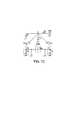
[0039]絶対静電容量検知は、センサ電極から実質的に一定の電圧(すなわち系統接地又は任意の他の実質的に一定の電圧)までの静電容量を測定することによって行うことができる。図1B〜1Gは、静電容量検知を行う際に使用することが可能な、A、B、C、及びGNDの4つのノードを含む回路網を示す。図1Bは例えば、そのような4つのノードを含む回路網に存在し得る各種の静電容量を示す。図に示すように、この4ノードの回路網には6つの静電容量が示される。本明細書ではノードAを図1Bでセンサ電極と呼ぶが(変調信号で駆動されるため)、ノードA、B、又はCのどれをセンサ電極として使用してもよい。図1Bで、センサ電極(ノードA)はCAと並列なGNDまでの静電容量CFを有する。静電容量CFは、センサ電極に入力物体が近接することに基づいて変化する。したがって、CFを測定することによって近傍にある入力物体の位置を判定することができる。この説明を通じてノードAとセンサ電極は同義で使用することができる。Protection signal
[0039] Absolute capacitance sensing can be performed by measuring the capacitance from the sensor electrode to a substantially constant voltage (ie, system ground or any other substantially constant voltage). 1B-1G illustrate a network that includes four nodes A, B, C, and GND that can be used to perform capacitance sensing. FIG. 1B shows, for example, various capacitances that may exist in a network that includes four such nodes. As shown in the figure, six capacitances are shown in this four-node network. Although node A is referred to herein as a sensor electrode in FIG. 1B (because it is driven with a modulation signal), any of nodes A, B, or C may be used as the sensor electrode. In FIG. 1B, the sensor electrode (node A) has a capacitance CF to GND in parallel with CA. The capacitance CF changes based on the proximity of the input object to the sensor electrode. Therefore, it is possible to determine the position of the input object in the vicinity by measuring the CF. Throughout this description, node A and sensor electrode can be used interchangeably.
[0040]一実施形態では、センサ電極から近くの入力物体までの静電容量の変化は、センサ電極に変調信号(図ではV(t))を駆動してから、センサ電極で受け取られる、結果として生じる信号を測定することにより測定される。一実施形態では、結果として生じる信号は、結果として生じる電流i(t)に対応する。結果として生じる信号を測定することにより、入力物体の位置を求めることができる。しかし、図1Bに示す静電容量CA、CAB、CCA、CB、CBC、及び/又はCCはいくつかの悪影響を及ぼす可能性がある。例えば、センサ電極から接地までの総静電容量が増すと、センサ電極の整定時間が増大し、結果として生じる信号の静電容量の大きさも増し、その結果必要とされる検知回路のダイナミックレンジが拡大する。各種実施形態で、これらの静電容量の一部は可変である(プロセス、温度、印加されるDC電圧等により)可能性があり、それにより変動を補償することが難しくなる。多くの実施形態では、これらの他の静電容量を低減又は除去することで入力装置の性能を改善し、入力物体とセンサ電極の間の静電容量の変化をより容易に判定できるようにすることができる。[0040] In one embodiment, the change in capacitance from the sensor electrode to a nearby input object drives the modulation signal (V (t) in the figure) to the sensor electrode and then is received at the sensor electrode, resulting Is measured by measuring the resulting signal. In one embodiment, the resulting signal corresponds to the resulting current i (t). By measuring the resulting signal, the position of the input object can be determined. However, the capacitances CA , CAB , CCA , CB , CBC , and / or CC shown in FIG. 1B can have some adverse effects. For example, as the total capacitance from the sensor electrode to ground increases, the settling time of the sensor electrode increases and the resulting signal capacitance increases, resulting in the required dynamic range of the sensing circuit. Expanding. In various embodiments, some of these capacitances can be variable (depending on process, temperature, applied DC voltage, etc.), which makes it difficult to compensate for variations. In many embodiments, reducing or eliminating these other capacitances improves the performance of the input device, making it easier to determine the change in capacitance between the input object and the sensor electrode. be able to.
[0041]一実施形態では、さらに図1Bを参照すると、静電容量CFは、ノードA、すなわちセンサ電極を変調信号で駆動し、結果として生じる受信信号を測定することにより求めることができる。この駆動及び測定の段階中に、ノードB(すなわち別の電極)を浮遊状態にしておくか、又は実質的に一定の電圧(例えば接地等)を駆動するか、又は保護信号を駆動することができる。同様に、ノードCも浮遊状態にしておくか、実質的に一定の電圧(接地)を駆動するか、又は保護信号を駆動することができる。したがって、下の表1に示すように、測定時にはノード/電極BとCとの可能な組み合わせが9つあることになる。
[0042]寄生容量の影響を低減又は解消することで、図1B〜1Gに示していない寄生抵抗の存在を考慮すると、センサ電極(図1BのノードA)の整定時間が改善され、単位時間当たりの測定回数を増やすことが可能となり、信号対雑音比が高まる。静電容量CA、CB、CC、CAB、CBC、及びCCAの一部又はすべても、温度、プロセス、印加電圧、又は他の条件に応じて変化する可能性がある。この変動性を緩和することは、入力物体に起因して生じた静電容量の変化を正確に検出するために重要である。[0042] By taking into account the presence of parasitic resistance not shown in FIGS. 1B-1G by reducing or eliminating the effects of parasitic capacitance, the settling time of the sensor electrode (node A in FIG. 1B) is improved, per unit time The number of measurements can be increased, and the signal-to-noise ratio is increased. Some or all of the capacitances CA , CB , CC , CAB , CBC , and CCA can also vary depending on temperature, process, applied voltage, or other conditions. Alleviating this variability is important for accurately detecting changes in capacitance caused by the input object.
[0043]図1Bの別の実施形態では、CFの測定中にノードB及びCをオープンにしておく(ノードB及びCを電気的に浮遊状態にする)ことによりCFの測定を改善することができる。CA、CB、及びCCの値が結合静電容量CBCとCCAに対して小さい場合(例えば1桁小さい場合)は、一方のノードを保護し、他方のノードを浮遊状態にすることがより効果的になる。一方、ノードから接地までの静電容量の値が結合静電容量に対して大きい場合は、ノードを浮遊状態にすることの効果が低下する。[0043] In another embodiment of FIG. 1B, the measurement ofCF is improved by keeping nodes B and C open during measurement ofCF (by leaving nodes B and C electrically floating). be able to. If the values of CA , CB , and CC are small relative to the combined capacitances CBC and CCA (for example, one order of magnitude smaller), one node is protected and the other node is left floating. Is more effective. On the other hand, when the value of the capacitance from the node to the ground is larger than the combined capacitance, the effect of making the node floating is reduced.
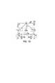
[0044]図1Cに示す実施形態では、静電容量CFは、ノードB及びCを接地した状態でノードAを変調信号で駆動し、結果として生じる信号を測定することにより求めることができる。ノードB及びCは接地されているので、静電容量CAB及びCCBは実質的に静電容量CF及びCAと並列であり、一方CB、CBC、及びCCは回路から実質的に除去される(点線の枠で示す)。静電容量CAB及びCCBは通例はCFに対して大きく、CFはCAB及びCCBと併せて測定されるため、受信モジュールの必要なダイナミックレンジが増大する。さらに、静電容量CAB及びCCBは抵抗センサ電極に沿って分散した静電容量であるため、センサ電極の整定時間も増大する。[0044] In the embodiment shown in FIG. 1C, capacitance CF can be determined by driving node A with a modulation signal with nodes B and C grounded, and measuring the resulting signal. Since nodes B and C are grounded, capacitances CAB and CCB are substantially in parallel with capacitances CF and CA , while CB , CBC and CC are substantially from the circuit. Removed (indicated by a dotted frame). CapacitanceC AB andC CB is typically greater relativeC F,C F is to be measured in conjunction withC AB andC CB, the required dynamic range of the receiver module is increased. Furthermore, since the capacitancesCAB andCCB are capacitances dispersed along the resistance sensor electrode, the settling time of the sensor electrode also increases.
[0045]或いは、図1Dに示すように、2つのV(t)電圧発生器で示すノードで保護信号を駆動することにより、ノードB及びC(電極B及びC)の両方を「保護」する。保護信号は、振幅、形状、位相、及び/又は周波数の少なくとも1つを変調信号V(t)と等しくすることができる。そのような実施形態では、ノードB及びCに接続された図1Dに示すすべての結合静電容量CAB、CBC、及びCCAの間の電圧は変化せず、したがってこれらの静電容量は実質的に回路から除去される。測定される静電容量は、CFと1つの静電容量CAとの合計である。多くの実施形態では、CAはCFと同じオーダーであり、そのため受信モジュールのダイナミックレンジを拡大する必要がなく、及び/又はセンサ電極の整定時間もCAのためにわずかに増大するだけであり、より高い変調信号又はトランスミッタ信号周波数を使用することが可能になる。保護には、温度や電圧に起因する静電容量CAB、CBC、及びCCAの変化の影響を解消するという重要な副次的な利益もある。[0045] Alternatively, as shown in FIG. 1D, both nodes B and C (electrodes B and C) are “protected” by driving a protection signal at a node represented by two V (t) voltage generators. . The protection signal may have at least one of amplitude, shape, phase, and / or frequency equal to the modulation signal V (t). In such an embodiment, the voltages between all of the coupled capacitances CAB , CBC , and CCA shown in FIG. 1D connected to nodes B and C do not change, and therefore these capacitances are Substantially removed from the circuit. The measured capacitance is the sum of CF and one capacitance CA. In many embodiments, CA is on the same order as CF , so there is no need to increase the dynamic range of the receiving module and / or the sensor electrode settling time is only slightly increased due to CA. Yes, it is possible to use higher modulation signals or transmitter signal frequencies. Protection also has an important side benefit of eliminating the effects of changes in capacitance CAB , CBC and CCA due to temperature and voltage.
[0046]一部の実施形態では、図1Eに示すように、保護信号がノードB及びCの一方に印加され、他方のノードB又はCは電気的に浮遊状態にする。この特定の実施形態では、保護信号は、図のV(t)電圧発生器で示されるようにノードBに印加される。静電容量CCは、CBC及びCCAに比べて小さいと想定され、したがってノードCはノードBに印加される保護信号で有効に駆動される。これにより回路からCCAが実質的に除去される。さらに、変調信号と保護信号はCBCとCCAの直列の組み合わせの両端に印加されるので、静電容量CBC及びCCAも等価回路から実質的に除去することができる。したがって、CCがCBC及びCCAと比べて小さい場合は、ノード/電極Bだけを保護し、一方ノード/電極Cは浮遊状態にしておくことが、ノード/電極B及びCの両方を保護することと実質的に同等となる可能性がある。[0046] In some embodiments, as shown in FIG. 1E, a protection signal is applied to one of nodes B and C, leaving the other node B or C electrically floating. In this particular embodiment, the protection signal is applied to node B as shown by the V (t) voltage generator in the figure. Capacitance CC is assumed to be small compared to CBC and CCA , so node C is effectively driven with a protection signal applied to node B. This substantially removes CCA from the circuit. Furthermore, the modulation signal and the protection signal so is applied across the series combination of CBC and CCA, it can be the capacitance CBC and CCA also substantially removed from the equivalent circuit. Therefore, if CC is smaller than CBC and CCA , only node / electrode B is protected, while node / electrode C is left floating, which protects both node / electrode B and C May be substantially equivalent to
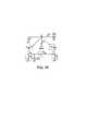
[0047]図1Fに示す実施形態では、ガード信号はノードB又はノードCに駆動され、一方ノードB又はノードCの他方は実質的に一定の電圧で駆動される(すなわち接地される)。ノードBが駆動されるので、静電容量CBは、結果として生じる信号には実質的に影響を与えず、またCBCの一方の端が駆動され、他方が接地されるため、CBCは結果として生じる信号には実質的に影響を与えない。さらに、ノードCが接地されるため、静電容量CCは結果として生じる信号に実質的に影響を与えない。さらに、CABの両端が同様の信号で駆動されるので、結果として生じる信号に影響を与えない。ただし、ノードCは実質的に一定の電圧で駆動され、ノードAは変調信号で駆動されるので、ノードCとノードA間の静電容量(CCA)は結果として生じる信号に影響する可能性がある。この実施形態は、例えば、ノードと接地間の静電容量値(例えばCC)が除去される一方で、結合静電容量(例えばCCA)は除去されない点で図1D及び図1Eと異なる。[0047] In the embodiment shown in FIG. 1F, the guard signal is driven to Node B or Node C, while the other of Node B or Node C is driven with a substantially constant voltage (ie, grounded). Since node B is driven, capacitance CB does not substantially affect the resulting signal, and because one end of CBC is driven and the other is grounded, CBC is The resulting signal is not substantially affected. Furthermore, since node C is grounded, the capacitance CC does not substantially affect the resulting signal. Furthermore, since both ends of the CAB is driven by the same signal, it does not affect the resulting signal. However, since node C is driven with a substantially constant voltage and node A is driven with a modulation signal, the capacitance (CCA ) between node C and node A can affect the resulting signal. There is. This embodiment differs from FIGS. 1D and 1E in that, for example, the capacitance value (eg, CC ) between the node and ground is removed, while the combined capacitance (eg, CCA ) is not removed.
[0048]図1Gは、ノードB及びノードCの一方が接地され、他方のノードを浮遊状態にする実施形態を示す。図の実施形態では、ノードBが接地されるので、静電容量CBは結果として生じる信号に影響を与えない。さらに、CCとCBCは並列であり、CCは多くの実施形態ではCBCよりも小さいため、CCは無視できる。これらの結果CAB、CA、及びCCAがCBCと直列になり、結果として生じる信号に影響する可能性がある。[0048] FIG. 1G illustrates an embodiment in which one of node B and node C is grounded and the other node is floating. In the illustrated embodiment, since node B is grounded, capacitance CB does not affect the resulting signal. Furthermore,C C andC BC is parallel,C C is smaller thanC BC in many embodiments,C C is negligible. These results CAB , CA , and CCA can be in series with CBC and affect the resulting signal.
[0049]表示装置の一実施形態では、画素に共有される電極が通例は、例えばVcom電極(すなわち(1つ又は複数の)共通電極)、ゲート電極(すなわちゲート線)、及びソース電極(すなわちソース線)の3つある。下記で詳細に述べるように、各種実施形態で、これらの電極のいずれでもセンサ電極として構成することができる。一実施形態では、図1B〜1Gで説明した4ノードの回路網は1つの副画素に対応することができるが、同様の説明を副画素の集合した群に適用することができる。例えば、ノードAをセンサ電極とし、これをディスプレイの更新にも使用する。ノードB及びCは、他の種の表示電極(例えば、ゲート電極及びソース電極)とすることができる。さらに、センサ電極に関連する静電容量は、関連する配線やその他の経路の静電容量も含むことができる。副画素に関連する静電容量は、4つのノード、すなわち、AC系統接地(各種図面では「GND」とも表記し、特殊記号で示す)、Vcom電極、ソース電極、及びゲート電極を含む回路網を含むことができる。 [0049] In one embodiment of the display device, the electrodes shared by the pixels are typically, for example, Vcom electrodes (ie, the common electrode (s)), gate electrodes (ie, gate lines), and source electrodes (ie, There are three source lines. As described in detail below, in various embodiments, any of these electrodes can be configured as a sensor electrode. In one embodiment, the four-node network described in FIGS. 1B-1G can correspond to one subpixel, but the same description can be applied to a group of subpixels. For example, the node A is used as a sensor electrode, which is also used for updating the display. Nodes B and C can be other types of display electrodes (eg, gate electrodes and source electrodes). Furthermore, the capacitance associated with the sensor electrode can also include capacitance of associated wiring and other paths. The capacitance associated with the sub-pixel is a network including four nodes, that is, an AC system ground (also referred to as “GND” in various drawings and indicated by a special symbol), a Vcom electrode, a source electrode, and a gate electrode. Can be included.
[0050]一実施形態では、各センサ電極は、共通電極層の1つ又は複数の部分(Vcom電極部分)、ソース線、及びゲート線からなり、上記説明のセンサ電極がノードAに相当し、ソース線がノードBに相当し、ゲート線がノードCに相当する。ソース線及び/又はゲート線は、保護信号を駆動するか、又は電気的に浮遊状態にして、それらの寄生容量の影響を少なくとも一部取り除くことができる。さらに、共通電極も保護信号で駆動して、その静電容量が、静電容量検知のために駆動されているセンサ電極に影響しないようにすることができる。これに対して、典型的な表示装置は、例えばノードB及びノードCが接地される図1Cに示すようにタッチ測定期間中にソース線とゲート線にDC電圧を駆動する。それに対して、図1D〜図1Fは、結合静電容量の1つ又は複数を除去するために表示電極の少なくとも1つに保護信号を駆動することを示す。 [0050] In one embodiment, each sensor electrode comprises one or more portions of a common electrode layer (Vcom electrode portion), a source line, and a gate line, and the sensor electrode described above corresponds to node A, The source line corresponds to the node B, and the gate line corresponds to the node C. The source line and / or gate line can drive a protection signal or be electrically floating to at least partially eliminate the effects of their parasitic capacitance. Furthermore, the common electrode can also be driven with a protection signal so that its capacitance does not affect the sensor electrode being driven for capacitance detection. On the other hand, a typical display device drives a DC voltage to the source line and the gate line during the touch measurement period as shown in FIG. In contrast, FIGS. 1D-1F illustrate driving a protection signal on at least one of the display electrodes to remove one or more of the combined capacitances.
[0051]別の実施形態では、センサ電極は(1つ又は複数の)Vcom電極(共通電極)とは別であり、Vcom電極に保護信号を駆動してVcom電極とセンサ電極間の寄生静電結合の影響を低減させる。さらに、ゲート線及び/又はソース線もすべて保護信号を駆動するか、又は電気的に浮遊状態にして、ゲート線とセンサ電極間、及びソース線とセンサ電極間の寄生容量の影響を低減することができる。 [0051] In another embodiment, the sensor electrode is separate from the Vcom electrode (s) (common electrode) and drives a protection signal to the Vcom electrode to cause parasitic electrostatics between the Vcom electrode and the sensor electrode. Reduce the effect of coupling. Furthermore, all the gate lines and / or source lines also drive a protection signal or are in an electrically floating state to reduce the influence of parasitic capacitance between the gate line and the sensor electrode and between the source line and the sensor electrode. Can do.
[0052]さらに他の実施形態では、第1のセンサ電極にトランスミッタ信号を駆動し、一方で結果として生じる、トランスミッタ信号に対応する影響を含んでいる信号を第2のセンサ電極で受信する。上記と同様の方式を第1のセンサ電極及び/又は第2のセンサ電極の近傍にある表示電極に適用することができる。送信電極(第1のセンサ電極)及び受信電極(第2のセンサ電極)から接地までの静電容量を低減又は除去することにより、送信電極及び/又は受信電極の整定時間を改善することができる。さらに、送信電極及び/又は受信電極と表示電極の間の静電容量の変動に基づく送信電極と受信電極間の静電容量値の変動を低減又は解消することができる。 [0052] In yet another embodiment, a transmitter signal is driven to the first sensor electrode while the resulting signal containing an effect corresponding to the transmitter signal is received at the second sensor electrode. A method similar to the above can be applied to the display electrode in the vicinity of the first sensor electrode and / or the second sensor electrode. By reducing or eliminating the capacitance from the transmission electrode (first sensor electrode) and the reception electrode (second sensor electrode) to ground, the settling time of the transmission electrode and / or the reception electrode can be improved. . Furthermore, the variation in the capacitance value between the transmission electrode and the reception electrode based on the variation in the capacitance between the transmission electrode and / or the reception electrode and the display electrode can be reduced or eliminated.
[0053]上記の説明はさらに、以下の説明で実施される各種構成に適用することができる。 [0053] The above description can be further applied to various configurations implemented in the following description.
センサ電極の配置
[0054]一実施形態では、センサ電極120は同じ基板の異なる面に配置することができる。例えば、(1つ又は複数の)センサ電極120は各々、基板の表面の1つに沿って長手方向に延在することができる。さらに、基板の一方の面ではセンサ電極120が第1の方向に延在するが、基板の他方の面ではセンサ電極120が第1の方向に対して平行又は直交する第2の方向に延在することができる。例えば、電極120は棒状又は縞状にすることができ、その場合、基板の一方の面の電極120は、基板の反対側の面のセンサ電極120に対して直交する方向に延在する。Sensor electrode placement
[0054] In one embodiment, the
[0055]センサ電極は、基板の両面に任意の所望の形状に形成することができる。さらに、基板の一方の面のセンサ電極120の大きさ及び/又は形状を、基板の別の面のセンサ電極120の大きさ及び/又は形状と異ならせることができる。また、同じ面にあるセンサ電極120が互いに異なる形状と大きさであってもよい。 [0055] The sensor electrodes can be formed in any desired shape on both sides of the substrate. Further, the size and / or shape of the
[0056]別の実施形態では、センサ電極120を異なる基板に形成し、その後共に積層することができる。一例では、基板の1つに配置された第1の複数のセンサ電極120を使用して検知信号を送信し(すなわち送信電極)、一方他方の基板に配置された第2の複数のセンサ電極120を使用して、生じる信号を受信することができる(すなわち受信電極)。他の実施形態では、第1及び/又は第2の複数のセンサ電極を絶対静電容量センサ電極として駆動することができる。一実施形態では、第1の複数のセンサ電極は第2の複数のセンサ電極よりも大きい(表面積が大きい)が、これは必要条件ではない。他の実施形態では、第1の複数のセンサ電極と第2の複数のセンサ電極は、似たような大きさ及び/又は形状を有することができる。したがって、一方の基板のセンサ電極120の大きさ及び/又は形状は、他方の基板の電極120の大きさ及び/又は形状と異なる可能性がある。その場合でも、センサ電極120はそれぞれの基板で任意の所望形状に形成することができる。また、同じ基板のセンサ電極120が異なる形状及び大きさであってもよい。 [0056] In another embodiment, the
[0057]別の実施形態では、センサ電極120がすべて共通の基板の同じ側又は面に配置される。一例では、第1の複数のセンサ電極が、第1の複数のセンサ電極が第2の複数のセンサ電極と交差する領域内にジャンパーを備え、ジャンパーは第2の複数のセンサ電極から絶縁される。上記のように、センサ電極120は各々同じ大きさ若しくは形状、又は異なる大きさ及び形状とすることができる。 [0057] In another embodiment, the
[0058]別の実施形態では、センサ電極120はすべて、共通の基板の同じ側又は面に配置され、検知領域170内で互いから隔離される。そのような実施形態では、センサ電極120は互いから電気的に隔離される。一実施形態では、電極120はマトリクス配列で配置され、各センサ電極120は実質的に同じ大きさ及び/又は形状である。そのような実施形態では、センサ電極120をマトリクスセンサ電極と呼ぶ場合がある。一実施形態では、センサ電極120のマトリクス配列にあるセンサ電極の1つ又は複数は、大きさ及び形状の少なくとも一方が異なる。マトリクス配列の各センサ電極は、静電画像の1画素に対応することができる。一実施形態では、処理システム110は、センサ電極120を変調信号で駆動して、絶対静電容量の変化を判定するように構成される。他の実施形態では、処理システム110は、センサ電極120のうち第1のセンサ電極にトランスミッタ信号を駆動し、結果として生じる信号をセンサ電極120のうち第2のセンサ電極で受信するように構成される。(1つ又は複数の)トランスミッタ信号と(1つ又は複数の)変調信号は、形状、振幅、周波数、及び位相の少なくとも1つを同様にすることができる。各種実施形態で、(1つ又は複数の)トランスミッタ信号と(1つ又は複数の)変調信号は同じ信号である。さらに、トランスミッタ信号は、トランスキャパシタンス検知に使用される変調信号である。各種実施形態で、1つ又は複数のグリッド電極を共通の基板上のセンサ電極120間に配置することができ、(1つ又は複数の)グリッド電極を使用してセンサ電極を防護及び保護することができる。 [0058] In another embodiment, the
[0059]本明細書で使用される「防護(shield)」とは、電極に一定の電圧を駆動することを言い、「保護する(guard)」とは、第1の電極の静電容量を測定するために第1の電極を変調する信号と振幅及び位相が実質的に同等の可変電圧信号を第2の電極に駆動することを言う。電極を電気的に浮遊状態にするとは、浮遊状態にすることにより第2の電極が静電結合を介して入力装置100内の第1又は第3の電極から所望の保護波長を受け取る場合の保護の一形態と解釈することができる。各種実施形態で、保護は防護のサブセットと考えることができ、したがって、センサ電極を保護するとそのセンサ電極の防護も行われる。グリッド電極は、可変の電圧、又は実質的に一定の電圧で駆動するか、又は電気的に浮遊状態にすることができる。グリッド電極はトランスミッタ信号で駆動される場合には送信電極としても使用することができ、グリッド電極と1つ又は複数のセンサ電極との間の静電結合を求めることができる。一実施形態では、グリッド電極とセンサ電極の間に浮遊電極を配置することができる。特定の一実施形態では、浮遊電極、グリッド電極、及びセンサ電極は、表示装置の共通電極全体からなる。他の実施形態では、グリッド電極をセンサ電極120とは別の基板若しくは基板の面、又はその両方に配置することができる。センサ電極120は基板上で電気的に隔離することができるが、電極は検知領域170の外側、例えばセンサ電極120に静電容量検知信号を送信又は受信する接続領域内では共に結合することができる。各種実施形態で、センサ電極120は、各種パターンを使用して配列として配置することができ、その場合、電極120のすべてが同じ大きさ及び形状ではない。さらに、配列内の電極120間の距離は等距離でなくともよい。 [0059] As used herein, "shield" refers to driving a constant voltage across an electrode, and "guard" refers to the capacitance of a first electrode. It means that a variable voltage signal having substantially the same amplitude and phase as that of a signal that modulates the first electrode is driven to measure the second electrode. Making the electrode electrically floating means protection when the second electrode receives a desired protection wavelength from the first or third electrode in the
[0060]上記のセンサ電極の配置のいずれでも、センサ電極120及び/又は(1つ又は複数の)グリッド電極は、表示装置160の外部の基板に形成することができる。例えば、電極120及び/又は(1つ又は複数の)グリッド電極は、入力装置100内のレンズの外側表面に配置することができる。他の実施形態では、センサ電極120及び/又は(1つ又は複数の)グリッド電極は、表示装置のカラーフィルタガラスと入力装置のレンズの間に配置される。他の実施形態では、センサ電極及び/又は(1つ又は複数の)グリッド電極の少なくとも一部を、薄膜トランジスタ基板(TFT基板)と表示装置160のカラーフィルタガラスの間に位置するように配置することができる。一実施形態では、第1の複数のセンサ電極及び/又は(1つ又は複数の)グリッド電極がTFT基板と表示装置160のカラーフィルタガラスの間に配置され、第2の複数のセンサ電極及び/又は(1つ又は複数の)第2のグリッド電極がカラーフィルタガラスと入力装置100のレンズの間に配置される。さらに他の実施形態では、センサ電極120及び/又は(1つ又は複数の)グリッド電極のすべてがTFT基板と表示装置のカラーフィルタガラスの間に配置され、センサ電極は上記のように同じ基板又は別の基板に配置することができる。 [0060] In any of the sensor electrode arrangements described above, the
[0061]1つ又は複数の実施形態では、少なくとも第1の複数のセンサ電極120は、ディスプレイの更新に使用される表示装置の1つ又は複数の表示電極からなる。例えば、センサ電極120は、Vcom電極の1つ又は複数の部分、ソース駆動線、ゲート線、アノード副画素電極若しくは陰極画素電極、又は他の表示素子などの共通電極からなる。これらの共通電極は適切なディスプレイ画面基板に配置することができる。例えば、共通電極は、何らかのディスプレイ画面(例えば、IPS(In Plane Switching)、FFS(Fringe FieldSwitching)、又はPLS(Plane to Line Switching)、有機発光ダイオード(OLED))内の透明基板(ガラス基板、TFTガラス、又は他の透明材料)、何らかのディスプレイ画面(例えば、PVA(Patterned Vertical Alignment)、MVA(Multi-domainVertical Alignment)、IPS、及びFFS)のカラーフィルタガラスの下部、陰極層(OLED)の上などに配置することができる。そのような実施形態では、共通電極は、複数の機能を行うことから、「複合電極」とも呼ぶことができる。各種実施形態で、各センサ電極120は、1つの画素又は副画素に関連付けられた1つ又は複数の共通電極からなる。他の実施形態では、少なくとも2つのセンサ電極120が、1つの画素又は副画素に関連付けられた少なくとも1つの共通電極を共有することができる。第1の複数のセンサ電極は、表示の更新と静電容量検知のために構成された1つ又は複数の共通電極からなることができるのに対し、第2の複数のセンサ電極は、静電容量検知を行うために構成し、表示の更新については構成しないことが可能である。さらに、1つ又は複数の実施形態で、存在する場合グリッド電極及び/又は浮遊電極は1つ又は複数の共通電極からなる。 [0061] In one or more embodiments, at least the first plurality of
[0062]或いは、すべてのセンサ電極120をTFT基板と表示装置160のカラーフィルタガラスの間に配置することができる。一実施形態では、第1の複数のセンサ電極がTFT基板に配置され、各々は1つ又は複数の共通電極からなり、第2の複数のセンサ電極をカラーフィルタガラスとTFT基板の間に配置することができる。具体的には、受信電極は、カラーフィルタガラスのブラックマスク内に配線することができる。別の実施形態では、すべてのセンサ電極120が1つ又は複数の共通電極からなる。センサ電極120はすべて、電極の配列としてTFT基板又はカラーフィルタガラスに配置することができる。上記のように、センサ電極120の一部はジャンパーを使用して配列内で共に結合するか、又はすべての電極120を配列内で電気的に隔離し、グリッド電極を使用してセンサ電極120を防護又は保護することができる。もう一つの実施形態では、存在する場合、グリッド電極は1つ又は複数の共通電極からなる。 Alternatively, all of the
[0063]上記のセンサ電極配置のいずれでも、センサ電極120は、入力装置100内で、センサ電極120を送信電極と受信電極に分けることによってトランスキャパシタンスモードで、又は絶対静電容量検知モードで、又はそれらのモードの何らかの混合で動作させることができる。 [0063] In any of the sensor electrode arrangements described above, the
[0064]下記で詳細に述べるように、センサ電極120又は表示電極(例えば、ソース線、ゲート線、又は基準(共通)線)の1つ又は複数を使用して防護又は保護を行うことができる。本明細書で使用する場合、防護とは、一定の電圧又はガード信号(可変電圧信号)を電極に駆動することと、入力装置100内の電極を浮遊状態にすることを言う。 [0064] As described in detail below, one or more of the
[0065]引き続き図1Aを参照すると、センサ電極120に結合された処理システム110はセンサモジュールを含み、各種実施形態で、処理システム110は、それに加えて、又はそれに代えて、ディスプレイドライバモジュールを備えることができる。センサモジュールは、入力の検知が要求される期間中に静電容量検知を行うためにセンサ電極120の少なくとも1つを駆動するように構成された回路を含む。一実施形態では、センサモジュールは、少なくとも1つのセンサ電極に変調信号を駆動して、その少なくとも1つのセンサ電極と入力物体の間の絶対静電容量の変化を検出するように構成される。別の実施形態では、センサモジュールは、少なくとも1つのセンサ電極にトランスミッタ信号を駆動して、その少なくとも1つのセンサ電極と別のセンサ電極の間のトランスキャパシタンスの変化を検出するように構成される。変調信号及びトランスミッタ信号は、一般に、入力検知のために割り当てられた時間にわたって複数回の電圧遷移を含む可変電圧信号であり、静電容量検知信号と呼ぶこともある。各種実施形態で、変調信号とトランスミッタ信号は、形状、周波数、振幅、及び/又は位相の少なくとも1つが互いと似ている。他の実施形態では、変調信号とトランスミッタ信号は、周波数、形状、位相、振幅、及び位相が互いと異なる。センサモジュールは、センサ電極120の1つ又は複数に選択的に結合することができる。例えば、センサモジュール204は、センサ電極120の少なくとも1つに結合され、絶対静電容量モード又はトランスキャパシタンス検知モードで動作することができる。 [0065] With continued reference to FIG. 1A, the
[0066]センサモジュールは、入力の検知が所望される期間内に、変調信号又はトランスミッタ信号に対応する影響を含んでいる、結果として生じる信号をセンサ電極120で受信するように構成された回路を含む。センサモジュールは、検知領域内の入力物体140の位置を判定するか、又は、検知領域内の入力物体140の位置を判定するために、結果として生じる信号を表す情報を含む信号を別のモジュール又はプロセッサ、例えば判定モジュールや電子装置のプロセッサ(すなわちホストプロセッサ)に提供することができる。 [0066] The sensor module includes a circuit configured to receive the resulting signal at the
[0067]ディスプレイドライバモジュールは、表示の更新期間中に表示装置160のディスプレイに表示画像更新情報を提供するように構成された回路を含む。一実施形態では、ディスプレイドライバは、少なくとも1つの表示電極を駆動して表示装置の一画素に関連する電圧を設定するように構成された表示電極(ソース電極、ゲート電極、及びVcom電極)に結合され、保護モードで少なくとも1つの表示電極を動作させて、複数のセンサ電極のうち第1のセンサ電極とその少なくとも1つの表示電極との間の結合静電容量の影響を緩和する。各種実施形態で、表示電極は、画素に対応する記憶素子に電圧を駆動するソース電極、画素に対応するトランジスタにゲート電圧を設定するゲート電極、及び、記憶素子に基準電圧を供給する共通電極の少なくとも1つである。 [0067] The display driver module includes circuitry configured to provide display image update information to the display of the
[0068]一実施形態では、センサモジュールとディスプレイドライバモジュールは、共通の集積回路(第1のコントローラ)の内部に備えることができる。別の実施形態では、センサモジュールとディスプレイドライバモジュールは、2つの別個の集積回路に備えられる。複数個の集積回路からなる実施形態では、表示更新期間、検知期間、トランスミッタ信号、表示更新信号等を同期させるように構成された同期化機構をそれらの回路の間に結合することができる。 [0068] In one embodiment, the sensor module and the display driver module may be provided within a common integrated circuit (first controller). In another embodiment, the sensor module and display driver module are provided in two separate integrated circuits. In embodiments comprising a plurality of integrated circuits, a synchronization mechanism configured to synchronize the display update period, the detection period, the transmitter signal, the display update signal, etc. can be coupled between the circuits.
表示電極の保護
[0069]図2A〜図2Eは、本明細書に記載される実施形態による静電容量を測定するための回路を説明する回路図である。具体的には、図2A〜図2Eは、上記のように絶対静電容量検知を行う場合の図1Aの入力装置100の回路モデルを表すことができる。本実施形態では絶対静電容量検知の文脈で保護信号を使用することについて述べるが、本開示はそれに限定されない。代わりに、トランスキャパシタンス検知時に、保護信号(すなわちトランスミッタ信号と同様の信号)を、静電容量検知時に使用されない下記の表示電極に送信することができる。それにより、電力消費を低減し、整定時間を改善することができる。Display electrode protection
[0069] FIGS. 2A-2E are circuit diagrams illustrating a circuit for measuring capacitance according to embodiments described herein. Specifically, FIGS. 2A to 2E can represent a circuit model of the
[0070]図2Aの図200で示すように、ノードDでは検知電圧がセンサ電極120の1つ又は複数に結合される。図200は、帰還コンデンサ(CFB)を備えた演算増幅器からなる積算器210を含む。積算器210は、センサ電極120と、図2AにおいてコンデンサCABSで表される自由空間(又はアース)との間の静電容量を測定する。この静電容量は、入力装置の検知領域の近くに入力物体が来ると変化する。一実施形態では、ノードEで変調信号を低電圧と高電圧の間で切り替えることができる。ノードEの電圧が変化すると、積算器は負端子を同じ電圧にする。積算器210の出力電圧に基づいて、入力装置は、静電容量CABS及びCPを蓄積するためにどれほどの電荷が流れなければならなかったかを判断し、したがって、それらの静電容量の値を判定する。他の実施形態では、代わりにCABSを測定するために、変調された電圧をノードEに印加することができる。さらに、図2A〜図2Fに示すように電流を測定してCABSの値を判定するために電圧を駆動するのに代えて、入力装置は電流を駆動して電圧を測定してもよい。CABSの測定に使用される特定の技術に関係なく、下記のようにセンサ電極及び/又は表示電極を保護することで性能を改善することができる。[0070] At node D, the sense voltage is coupled to one or more of the
[0071]図200は、寄生容量CPが積算器210によって得られる測定結果に影響する可能性があることも示している。上記で図1B〜図1Gとの関係で説明したように、寄生容量は静電容量CABSの変化に比べてはるかに大きい可能性があるため、積算器210は、そのような高い寄生容量CPに対処する技術を利用しないと静電容量CABSの変化を有効に識別できない可能性がある。図2Bの図250は、保護信号215が印加され、それにより高い寄生容量CPがある場合でも積算器210が静電容量CABSの変化を有効に識別することができる回路モデルを示す。[0071] FIG. 200 also illustrates that the parasitic capacitance CP can affect the measurement results obtained by the
[0072]図250では、上記のように、寄生容量CPはセンサ電極120と入力装置内の任意の電極205間の結合静電容量を表す。そのため、電極205は、現在は検知されていない別のセンサ電極、又は電極120の近傍にある表示電極、例えば入力装置内で表示画像を更新するために使用されるソース電極、Vcom電極、陰極電極、又はゲート電極である可能性がある。電極205とセンサ電極120の間の寄生容量が積算器210によって行われる絶対静電容量の測定に干渉するのを防ぐために、電極205に保護信号を直接又は間接的に印加することができる。具体的には、保護信号は、電極120に駆動される変調信号と同とするか又は実質的に同様とすることができる。したがって、寄生容量の両端の電圧が変化しない場合(すなわち静電容量CPの一方の側の電圧が他方の側の電圧と同じ量だけ変化する場合)は、静電容量CPは積算器210で取得される測定結果に影響しない。例えば、ノードEで、低い検知電圧と高い検知電圧間の切り替えによって変調信号が定義される場合は、それと同じ電圧変化を保護信号として電極205に印加することができる。In [0072] Figure 250, as described above, the parasitic capacitance CP represents the coupling capacitance between any
[0073]一実施形態では、ノードD又はノードEを電気的に電極205と結合して、電極120に駆動される変調信号と同じ変調信号を保護信号として電極205に駆動するが、これは必要条件ではない。例えば、同期された他の駆動回路を使用して、電極120に駆動される変調信号と実質的に同様の(すなわち同じ位相及び/又は周波数及び/又は振幅)保護信号を電極205に駆動することができる。 [0073] In one embodiment, node D or node E is electrically coupled to
[0074]図2Cに示す図260では、センサ電極が表示電極(例えば、ソース電極、ゲート電極、又はVcom(若しくは陰極)電極)と別である。電極間が近接しているために、センサ電極(図2Cでは第1のセンサ電極として示す)と入力装置内のその他の電極との間に寄生容量が存在する可能性がある。言い換えると、図2Cの寄生容量は、第1のセンサ電極と、第2のセンサ電極との間(CSE)、Vcom電極との間(CVCOM)、ソース電極との間(CS)、及びゲート電極との間(CG)の結合静電容量の組み合わせになる。絶対静電容量を測定する際にこれらの寄生容量の影響を緩和するために、これらの電極に1つ又は複数の保護信号を直接又は間接的に駆動する。[0074] In FIG. 260, shown in FIG. 2C, the sensor electrode is separate from the display electrode (eg, source electrode, gate electrode, or Vcom (or cathode) electrode). Due to the proximity of the electrodes, there may be parasitic capacitance between the sensor electrode (shown as the first sensor electrode in FIG. 2C) and the other electrodes in the input device. In other words, the parasitic capacitance in FIG. 2C is between the first sensor electrode and the second sensor electrode (CSE ), between the Vcom electrode (CVCOM ), between the source electrode (CS ), And (CG ) coupling capacitance between the gate electrode and the gate electrode. In order to mitigate the effects of these parasitic capacitances when measuring absolute capacitance, one or more protection signals are driven directly or indirectly on these electrodes.
[0075]一実施形態では、第1のセンサ電極は、複数の受信電極の1つ又は複数であり、第2のセンサ電極は複数の送信電極の1つ又は複数である。他の実施形態では、第1及び第2のセンサ電極は、共通の複数のセンサ電極(例えば、送信電極、受信電極、又はマトリクスセンサ電極)のうちの第1及び第2のセンサ電極である。別の実施形態では、第1のセンサ電極は、複数の送信電極の1つ又は複数であり、第2のセンサ電極は複数の受信電極の1つ又は複数である。他の実施形態では、第1のセンサ電極はある種類のマトリクスセンサ電極であり、第2のセンサ電極はそれと同じ種類のマトリクスセンサ電極である。さらに他の実施形態では、第1のセンサ電極は複数のマトリクスセンサ電極1つ又は複数であり、一方第2のセンサ電極は1つ又は複数のグリッド電極である。さらに、第1のセンサ電極はある種類のマトリクスセンサ電極であり、一方第2のセンサ電極は第2の別の種類のマトリクスセンサ電極である。図2Cには示さないが、第2のセンサ電極、Vcom電極、ソース電極、及びゲート電極の1つがさらに別のセンサ電極に静電容量結合する可能性があり、それによりセンサ電極の寄生容量が増大する可能性がある。[0075] In one embodiment, the first sensor electrode is one or more of a plurality of receiving electrodes and the second sensor electrode is one or more of a plurality of transmitting electrodes. In other embodiments, the first and second sensor electrodes are first and second sensor electrodes of a plurality of common sensor electrodes (e.g., transmit electrodes, receive electrodes, or matrix sensor electrodes). In another embodiment, the first sensor electrode is one or more of the plurality of transmit electrodes and the second sensor electrode is one or more of the plurality of receive electrodes. In other embodiments, the first sensor electrode is a type of matrix sensor electrode and the second sensor electrode is the same type of matrix sensor electrode. In still other embodiments, the first sensor electrode is one or more matrix sensor electrodes, while the second sensor electrode is one or more grid electrodes. Furthermore, the first sensor electrode is a type of matrix sensor electrode, while the second sensor electrode is a second different type of matrix sensor electrode. Although not shown in FIG. 2C, one of the second sensor electrode, the Vcom electrode, the source electrode, and the gate electrode may be capacitively coupled to another sensor electrode, thereby causing a parasitic capacitance of the sensor electrode. May increase.
[0076]図2Dに示す図270では、センサ電極の第2のセンサ電極が、表示の更新に使用される表示装置の1つ又は複数の共通電極(ここではVcom/センサ電極として示す)と、表示装置の更新には使用されない入力センサ及び第1のセンサ電極からなる。図に示すように、第1のセンサ電極は表示装置のVcom/センサ電極、ソース電極、及びゲート電極に静電容量結合される。したがって、変調信号が第1のセンサ電極に駆動される時に、(1つ又は複数の)保護信号もVcom/センサ電極、ソース電極、及びゲート電極に駆動して、それにより絶対静電容量CABSを測定する際に寄生容量の影響を緩和することができる。図2Dには示さないが、第1及び第2のセンサ電極が共通の複数のセンサ電極からなる場合には第1のセンサ電極と第2のセンサ電極の間、又は第1のセンサ電極とグリッド電極の間に別の寄生容量が存在する可能性がある。さらに、第2のセンサ電極、Vcom電極、ソース電極、及びゲート電極の1つがさらに別のセンサ電極に静電容量結合する可能性があり、それによりセンサ電極の寄生容量が増大する可能性がある。[0076] In FIG. 270, shown in FIG. 2D, the second sensor electrode of the sensor electrode is one or more common electrodes (shown here as Vcom / sensor electrodes) of the display device used for display updates; It consists of an input sensor and a first sensor electrode that are not used for updating the display device. As shown, the first sensor electrode is capacitively coupled to the Vcom / sensor electrode, source electrode, and gate electrode of the display device. Thus, when the modulation signal is driven to the first sensor electrode, the protection signal (s) are also driven to the Vcom / sensor electrode, the source electrode, and the gate electrode, thereby providing an absolute capacitance CABS. When measuring the effect of parasitic capacitance can be mitigated. Although not shown in FIG. 2D, when the first and second sensor electrodes are composed of a plurality of common sensor electrodes, the first sensor electrode and the grid are arranged between the first sensor electrode and the second sensor electrode. There may be another parasitic capacitance between the electrodes. In addition, one of the second sensor electrode, the Vcom electrode, the source electrode, and the gate electrode may be capacitively coupled to another sensor electrode, thereby increasing the parasitic capacitance of the sensor electrode. is there.
[0077]一実施形態では、入力装置は、第2のセンサ電極(Vcom/センサ電極)とアース間の絶対静電容量も測定することができる。その場合は、第2のセンサ電極に変調信号を駆動し、第1のセンサ電極に保護信号を駆動することができる。言い換えると、すべてのセンサ電極に同時に変調信号を駆動するのではなく、1回の検知周期中に第1のセンサ電極に保護信号を駆動しながら回路が第2のセンサ電極だけで絶対静電容量検知を行い、次の検知周期にそれを逆転させて、第2のセンサ電極に保護信号を送りながら、第1のセンサ電極に関連する絶対静電容量を測定する。 [0077] In one embodiment, the input device can also measure the absolute capacitance between the second sensor electrode (Vcom / sensor electrode) and ground. In that case, the modulation signal can be driven to the second sensor electrode, and the protection signal can be driven to the first sensor electrode. In other words, instead of simultaneously driving the modulation signal to all the sensor electrodes, the circuit drives the protection signal to the first sensor electrode during one detection cycle, and the circuit has only the second sensor electrode for absolute capacitance. The detection is performed and reversed at the next detection cycle, and the absolute capacitance associated with the first sensor electrode is measured while sending a protection signal to the second sensor electrode.
[0078]図2Eは、すべてのセンサ電極が表示装置の1つ又は複数の共通電極からなる回路380を示す。ただし、他の実施形態では、センサ電極はソース又はゲート電極とすることができる。例えば、センサ電極は、電極の配列として同じ基板(若しくは同じ面)に配置しても、又は表示装置の複数の面に分散させてもよい。第1のセンサ電極間(すなわち共通電極又はVcom/センサ電極)の寄生容量は、共通電極と、ソース電極、ゲート電極、及び第1のセンサ電極と同じ方式で駆動されない近傍センサ電極との間の結合静電容量を含む可能性がある。それらの寄生容量間の電圧が変化しないようにするために、ソース電極、ゲート電極、及び近傍電極に直接又は間接的に保護信号を駆動することができる。近傍のセンサ電極はグリッド電極又は第2のセンサ電極からなる可能性がある。また、センサ電極と追加的な近傍センサ電極の間に寄生容量が存在する可能性もあり、この場合、第1の近傍センサ電極は別のセンサ電極であり、第2の近傍センサ電極はグリッド電極である可能性がある。さらに、近傍センサ電極、ソース電極、及びゲート電極の1つがさらに別のセンサ電極に静電容量結合する可能性があり、それがセンサ電極の寄生容量に影響する可能性がある。 [0078] FIG. 2E shows a circuit 380 in which all sensor electrodes consist of one or more common electrodes of the display device. However, in other embodiments, the sensor electrode can be a source or gate electrode. For example, the sensor electrodes may be arranged on the same substrate (or the same surface) as the electrode arrangement, or may be distributed on a plurality of surfaces of the display device. The parasitic capacitance between the first sensor electrodes (ie, the common electrode or Vcom / sensor electrode) is between the common electrode and the source sensor, the gate electrode, and a neighboring sensor electrode that is not driven in the same manner as the first sensor electrode. May include coupled capacitance. In order to prevent the voltage between the parasitic capacitances from changing, a protection signal can be directly or indirectly driven to the source electrode, the gate electrode, and the neighboring electrode. The nearby sensor electrode may consist of a grid electrode or a second sensor electrode. There may also be parasitic capacitance between the sensor electrode and the additional proximity sensor electrode, where the first proximity sensor electrode is another sensor electrode and the second proximity sensor electrode is a grid electrode. There is a possibility. In addition, one of the proximity sensor electrode, the source electrode, and the gate electrode can be capacitively coupled to another sensor electrode, which can affect the parasitic capacitance of the sensor electrode.
[0079]さらなる実施形態では、図2Fに示すように、第1のセンサ電極(送信電極)にトランスミッタ信号を駆動し、一方結果として生じる、トランスミッタ信号に対応する影響を含んでいる信号が第2のセンサ電極(受信電極)で受信される。回路290では、送信電極は少なくとも1つの共通電極からなる。さらに、受信電極は少なくとも1つの共通電極からなることが可能であるが、各種実施形態で、受信電極は共通電極とは別個にすることができる。送信電極(第1のセンサ電極)からソース/ゲート電極までの静電容量を低減又は解消することにより、送信電極の整定時間を改善することができる。図に示すように、ソース電極及び/又はゲート電極は、送信電極とソース電極及び/又はゲート電極との間の寄生容量CTS及びCTGが減るか、又はなくなるように、保護信号を駆動することができる。図2Fには示さないが、送信電極がVcom電極と別である場合には、受信電極とVcom電極の間に追加的な寄生容量が存在する可能性がある。[0079] In a further embodiment, as shown in FIG. 2F, the transmitter signal is driven to the first sensor electrode (transmitting electrode), while the resulting signal containing an effect corresponding to the transmitter signal is a second signal. Are received by the sensor electrode (receiving electrode). In the
[0080]図2C〜2Fでは各種表示電極及びセンサ電極に同じ保護信号を駆動しているが、これは説明を容易にするためである。他の実施形態では、表示電極とセンサ電極の両端のDC電圧を固有にすることができる。したがって、保護信号をそれらの電極に駆動すると、電極のDC電圧は同じように変化するだけで、等しい電圧にはならない。例えば、保護信号は、ソース電極、ゲート電極、及びVcom電極の各電圧を4Vずつ増加させるが、結果として生じる各電極の電圧は、例えばそれぞれ−1V、3V、及び5V等と異なる可能性がある。したがって、寄生容量の影響の緩和は、各種電極の絶対電圧に依存するのではなく、寄生容量両端の電圧は実質的に変化しない。 [0080] In FIGS. 2C-2F, the same protection signal is driven for the various display electrodes and sensor electrodes for ease of explanation. In other embodiments, the DC voltage across the display and sensor electrodes can be unique. Therefore, when the protection signal is driven to those electrodes, the DC voltage of the electrodes will change in the same way and not equal. For example, the protection signal increases each voltage of the source electrode, the gate electrode, and the Vcom electrode by 4V, but the resulting voltage of each electrode may be different from, for example, −1V, 3V, and 5V, respectively. . Therefore, the relaxation of the influence of the parasitic capacitance does not depend on the absolute voltages of the various electrodes, and the voltage across the parasitic capacitance does not substantially change.
[0081]また、保護信号は、静電結合を利用して異なる電極間で伝達することができる。例えば、Vcom電極及びゲート電極は、表示装置内で互いに隣接する層に配置される場合がある。そのため、保護信号はそれらの電極の一方の組だけに駆動すれば、電極間の静電結合に依拠して両方の電極の組に保護信号を伝搬させることができる。 [0081] The protection signal can also be transmitted between different electrodes using electrostatic coupling. For example, the Vcom electrode and the gate electrode may be disposed in layers adjacent to each other in the display device. Therefore, if the protection signal is driven to only one set of these electrodes, the protection signal can be propagated to both sets of electrodes depending on the electrostatic coupling between the electrodes.
[0082]さらに、図2B〜2Fの実施形態のいずれでも、寄生静電結合に寄与する表示電極及びセンサ電極の1つに実質的に一定の信号を駆動し、一方その他の電極には図1B〜1Gで説明したように保護信号を駆動する。さらに、図2B〜2Fの実施形態のいずれでも、寄生静電結合に寄与する表示電極及びセンサ電極の少なくとも1つを電気的に浮遊状態にし、一方その他の電極は図1B〜1Gで説明したように保護信号を駆動するか、電気的に浮遊状態にする。 [0082] In addition, in any of the embodiments of FIGS. 2B-2F, a substantially constant signal is driven to one of the display and sensor electrodes that contribute to parasitic electrostatic coupling, while the other electrode is driven to FIG. 1B. Drive protection signal as described in ~ 1G. Further, in any of the embodiments of FIGS. 2B-2F, at least one of the display electrodes and sensor electrodes that contribute to parasitic electrostatic coupling is electrically floating, while the other electrodes are as described in FIGS. 1B-1G. The protection signal is driven to an electrical floating state.
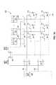
[0083]図3A〜3Bは、本明細書に記載される実施形態による、静電容量検知時に表示電極を保護するディスプレイシステムの概略ブロック図である。具体的には、ディスプレイシステム300は、ゲート選択ロジック305、及び画素315に結合された複数のソースドライバ310を含む。例えば、システム300は、図1Aで説明した入力装置100の表示装置の一部とすることができる。ゲート選択ロジック305(行選択ロジックとも呼ぶ)は、画素315内の個々のトランジスタスイッチを作動させることによりゲート電極325(又は行)の1つを選択することができる。オンの時、それらのスイッチは、ソースドライバ310がコンデンサ320の両端に所望の電圧を駆動することが可能な導電経路を実現する。コンデンサ320の電圧は、ソースドライバ310に接続されたソース電極330(又はカラム線)の電圧と、共通電極350における基準電圧(例えばVcom)との間の電圧差によって定義される。一実施形態では、コンデンサ320の静電容量は、画素315に対応する色を設定するために使用される液晶材料に少なくとも部分的に基づくことができる。ただし、本明細書に記載される実施形態はどの特定のディスプレイ技術にも限定されず、例えばLED、OLED、CRT、プラズマ、EL、又は他のディスプレイ技術に使用することができる。 [0083] FIGS. 3A-3B are schematic block diagrams of a display system that protects display electrodes during capacitance sensing according to embodiments described herein. Specifically, the
[0084]ゲート選択ロジック305は、すべての画素が更新されるまでディスプレイ画面の個々の行をラスタ走査することができる(これを本明細書では表示フレームの更新と呼ぶ)。例えば、ゲート選択ロジック305は、1つのゲート電極325又は行を導通させることができる。それに応じて、ソースドライバ310は、ソース電極330にそれぞれの電圧を駆動し、それにより導通状態になった行のコンデンサ320の両端に所望の電圧(基準電圧に対して)を生じさせる。そしてゲート選択ロジック305はその行を非導通状態にしてから次の行を導通させることができる。そのようにして、ゲート選択ロジック305及びソースドライバ310は、例えば処理システムのディスプレイドライバモジュールによって制御され、ゲート選択ロジック305が各行を導通させると、ソースドライバ310が画素315に適正な電圧を供給する。 [0084] The
[0085]静電容量検知を行う際、より具体的には絶対静電容量検知を行う際には、ゲート電極、ソース電極、及び共通電極325、330、350が保護信号を送信することができる。システム300は、マルチプレクサ340(すなわちMUX)を含み、これを使用して表示電極に保護信号を送信することができる。例えば、静電容量検知を行う際、表示装置は、MUX340を制御する選択信号を切り替えて、保護信号が表示電極、すなわちゲート電極、ソース電極、及び共通(又は陰極)電極325、330、350に送信されるようにする。図ではシステム300はすべての表示電極に保護信号を送信しているが、他の実施形態では、電極の1つ又は複数のみを選択して保護信号を搬送させ、一方その他の表示電極は任意で電気的に浮遊状態にする。例えば、センサ電極とソース電極330間の結合静電容量がセンサ電極とゲート電極325間の結合静電容量と比べてはるかに大きい場合、保護信号はソース電極330のみに駆動し、ゲート電極は駆動するか、又は電気的に浮遊状態にすることができる。 [0085] When performing capacitance detection, more specifically, when performing absolute capacitance detection, the gate electrode, the source electrode, and the
[0086]図3Bは、電荷共有システムを使用して、ソース電極330及び共通電極350に保護信号を駆動するディスプレイシステム390の使用を説明する図である。静電容量検知を行う際、ディスプレイシステム390は、ロジック、例えば制御ロジック345、及び電荷共有システムなどのディスプレイシステム390にすでに含まれているスイッチ素子335を使用することができる。静電容量検知時にこのロジックを使用するために、制御ロジック345は、ソースドライバをオフにし、スイッチ素子335を作動させて、共通電極350がソース電極330に接続されるようにする。また、制御ロジック345は、スイッチ340(ここではMUXとして示す)に、共通電極350に保護信号215を駆動するように指示する。すなわち、共通電極350を基準電圧Vcomに結合する代わりに、共通電極350が保護信号を送信する。共通電極350とソース電極330がスイッチ素子335を介して接続されるので、保護信号はソース線330にも駆動される。このようにして、静電容量検知を行う際に、ディスプレイシステム390内のスイッチ素子335は、ソース電極及び共通電極330、350とセンサ電極(図示せず)間の寄生容量をなくすために、ソース電極及び共通電極330、350に保護信号を送信できるようにする。 [0086] FIG. 3B is a diagram illustrating the use of a
[0087]図3Bではスイッチ340を使用して基準電圧と保護信号間を切り替えるものと示すが、これは例示の目的に過ぎない。他の実施形態では、共通電極350を、基準電圧又は保護信号を共通電極350に駆動することが可能なドライバに結合することができる。したがって、基準及びソース電極330に保護信号を送信するためにディスプレイシステム390に追加的なハードウェアを追加する必要がない。さらに、図3Bにはディスプレイシステム390は例えば電荷共有システムを含む場合にソース電極及び共通電極330、350に保護信号を送信する一例のみを示す。別の実施形態では、ディスプレイシステムが電荷共有システムを備えない場合でも、ソースドライバ310を使用して各ソース電極330に保護信号を駆動することができ、一方別のドライバ(図示せず)が共通電極350に保護信号を送信する。すなわち、ソース電極330が互いと結合されない、又は共通電極350と結合されない場合でも、表示電極に保護信号を送信するようにディスプレイシステムを構成することができる。 [0087] Although FIG. 3B shows that
[0088]例えば、共通電極350に保護信号が駆動される時に、ゲート電極325及び/又はソース電極330は電気的に浮遊状態にして、センサ電極からのそれらの静電容量を有効に除去することができる。別の例では、共通電極350及びゲート電極325に保護信号を駆動し、一方ソース電極330を電気的に浮遊状態にすることができる。他の例では、共通電極350及びソース電極330に保護信号を駆動し、一方ゲート電極325を電気的に浮遊状態にすることができる。さらに別の例では、ゲート電極325に保護信号を駆動し、一方ソース電極330及び/又は共通電極350を電気的に浮遊状態にする。別の例では、ゲート電極325及びソース電極330に保護信号を駆動し、一方共通電極350を電気的に浮遊状態にすることができる。さらに他の例では、ソース電極330に変調信号を駆動し、一方ゲート電極325及び/又は共通電極350を電気的に浮遊状態にすることができる。上記の例では、電気的に浮遊状態にする(1つ又は複数の)電極は、(1つ又は複数の)浮遊電極と駆動される(1つ又は複数の)電極の間の結合静電容量を介して保護信号で変調される。他の例では、電極(共通電極350、ゲート電極325、及びソース電極330)の1つにガード信号が駆動される時には、少なくとも1つの他の電極が実質的に一定の電圧で駆動される。 [0088] For example, when a protection signal is driven to the
[0089]一実施形態では、センサ電極の1つ又は複数が図3A及び3Bに示すディスプレイシステムで使用されるカラーフィルタガラスと入力装置の入力面との間に配置される。一実施形態では、1組のセンサ電極が、表示装置のカラーフィルタガラスと入力装置の入力面との間に配置される。表示装置内の電極は、表示装置の1つ又は複数の表示電極からなることができ、すなわち、それらの電極は表示の更新と静電容量検知を行う際の両方に使用される。さらに別の実施形態では、センサ電極の1つ又は複数が表示装置の活性層とカラーフィルタガラスとの間に配置され、センサ電極は表示装置の表示電極としても使用することができる。ゲートインパネル(gate-in-panel)システムでは、入力装置は、静電容量検知中にゲート電極を切り替えて高インピーダンス状態にすることができる。 [0089] In one embodiment, one or more of the sensor electrodes are disposed between the color filter glass used in the display system shown in FIGS. 3A and 3B and the input surface of the input device. In one embodiment, a set of sensor electrodes is disposed between the color filter glass of the display device and the input surface of the input device. The electrodes in the display device can consist of one or more display electrodes of the display device, i.e., they are used both for display updates and capacitance sensing. In yet another embodiment, one or more of the sensor electrodes are disposed between the active layer of the display device and the color filter glass, and the sensor electrode can also be used as a display electrode of the display device. In a gate-in-panel system, the input device can switch the gate electrode to a high impedance state during capacitance sensing.
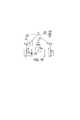
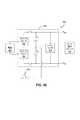
[0090]図4A〜4Bは、本明細書に記載される実施形態による、ディスプレイシステム内でゲート電極を保護するためのタッチ及びディスプレイ一体型コントローラ400を示す。具体的には、コントローラ400は、図3Aのディスプレイシステム300に結合して、ゲート選択ロジック305に結合されたゲート電極325に保護信号を駆動することができる。一実施形態では、コントローラ400は、図1Aに示す処理システム110とすることができる。さらに、コントローラ400は、入力装置内で静電容量検知と表示の更新の両方を行うために必要なロジックを含むことができる。例えば、コントローラ400は単一のICチップとすることができる。図には示さないが、コントローラ400は、上記のようにソース電極及び共通電極に保護信号を駆動するための制御信号を発行する、図3Aに示す制御ロジック345を含むことができる。 [0090] FIGS. 4A-4B illustrate an integrated touch and
[0091]一体型コントローラ400は、電源405及び電力変換器410を含む。電源405は、コントローラ400の外部にあってもよく、図3Aに示すゲート電極325の電圧を発生させるために電力変換器410に電力信号を供給する。ここで、電力変換器410は、高ゲート電圧VGH及び低ゲート電圧VGLを生成し、図3Aのゲート選択ロジック305がそれを使用して画素315の行を導通又は非導通状態にすることができる。一実施形態では、一体型コントローラ400はソースドライバ310を含むことができる。したがって、一体型コントローラ400は、ソース電圧(VS)並びにゲート電圧VGH及びVGLをディスプレイ画面に供給することができる。一実施形態では、保護信号は、表示電極を駆動する回路に送られる電源電圧を変調することにより直接又は間接的に生成することができる。[0091] The integrated
[0092]図4Bは、コントローラ400のより詳細な回路モデルを示す。具体的には、チャージポンプ420はゲート電圧VGH及びVGLを生成する。例えば、電源405は、ゲート電圧VGH及びVGLを生成するチャージポンプ420に電力を供給する。一実施形態では、VGHはおよそ15Vであり、一方VGLは−10Vである。保護信号215をゲート電圧に挿入するために、電力変換器410は、リザーバコンデンサC1とC2の間に結合されたノードを含む。これらのコンデンサは保護信号215を、電力変換器410で生成されたDCゲート供給電圧に結合する。一実施形態では、このノードは共通電極に結合することができる。したがって、このようにして、ゲート電圧VGH及びVGLに保護信号215を駆動することができる。保護信号215が送信されない時、コンデンサC1とC2の間のノードは代わりにDC電圧に接続することができる。一実施形態では、回路(例えばレベルシフタ415)は、個々の構成要素が、保護信号215によって誘発される電圧の変動に確実に耐えられるように設計することができる。さらに、レベルシフタ415は、ディスプレイドライバモジュールからゲート選択ロジック305へのクロック及び制御信号をレベルシフトするために使用することができ、電源に結合されて、制御信号が電力信号(VGH及びVGL)と同じように変調されることを保証する。それにより、制御信号も自動的に保護される。[0092] FIG. 4B shows a more detailed circuit model of the
[0093]図3A〜3B及び4A〜4Bに示すように、表示電極(すなわちソース電極、ゲート電極、及び共通電極)は保護信号215を駆動することにより、それらの電極とセンサ電極の間の寄生容量を除去することができる。さらに、表示電極に保護信号を適切に駆動することにより、画素コンデンサ320に蓄えられた電圧が影響を受けず、したがって、一体型ディスプレイ画面に現在表示されている画像が変化しない。言い換えると、保護信号は表示電極の電圧を同じように変化させる、すなわち表示電極における電圧の変動が同じであるため、画素トランジスタはオフのままとなり、それにより、画素の電圧が損失することを阻止する。したがって、コンデンサ320両端の電圧電位は変化せず、それにより表示画像を維持する。一例示的実施形態では、ゲートオフ電圧VGLは、−10Vから−6Vまで変動し、Vcom/ソース線は、4Vのピーク間保護信号に基づいて0Vから4Vまで変動する。[0093] As shown in FIGS. 3A-3B and 4A-4B, the display electrodes (ie, the source electrode, the gate electrode, and the common electrode) drive parasitic signals between the electrodes and the sensor electrode by driving the
[0094]保護信号が選択的に表示電極に印加された場合、例えば共通電極だけに印加される場合、保護信号は、信号が画素によって表示されている画像を破損させないように設計することができる。例えば、共通電極がゲート電極の電圧に対して負側に駆動され過ぎた場合は、スイッチが作動し、画素から電荷を失わせることができる。画素で電荷が失われることは、保護信号を正側の方向のみに駆動する、又はゲートオフ電圧を減らしてトランジスタが作動しないようにすることによっても防ぐことができる。 [0094] When a protection signal is selectively applied to the display electrodes, for example when applied only to the common electrode, the protection signal can be designed so that the signal does not damage the image displayed by the pixel. . For example, when the common electrode is driven too negatively with respect to the voltage of the gate electrode, the switch is activated and the charge can be lost from the pixel. The loss of charge in the pixel can also be prevented by driving the protection signal only in the positive direction or by reducing the gate-off voltage so that the transistor does not operate.
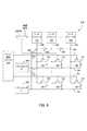
[0095]図5は、本明細書に記載される実施形態による、静電容量検知を行うために表示電極が使用されるディスプレイシステム500の概略ブロック図である。具体的には、ディスプレイシステム500は、表示を更新する際に使用される電極を静電容量検知を行う際にセンサ電極としても使用できることを示している。一実施形態では、コンデンサ320に結合された共通電極350を図1Aに示すセンサ電極120の1つ又は複数として使用することができる。すなわち、センサ電極をディスプレイ画面の上に配置するのではなく、共通電極350がセンサ電極の1つ又は複数として働くことができる。共通電極350に選択的に変調信号を駆動するために、ディスプレイシステム500は、それぞれの共通電極350に結合された複数のトランスミッタ505を含む。スイッチ素子510を使用して、各共通電極350をその他の電極350から電気的に隔離し、それにより1つのトランスミッタ505が共通電極350に固有の信号を駆動し、一方その他のトランスミッタ505はその他の電極に別の信号を駆動することができる。 [0095] FIG. 5 is a schematic block diagram of a
[0096]例えば、共通電極350が現在絶対静電容量検知用のセンサ電極として使用されている場合、トランスミッタ505は共通電極350に変調信号を送信することができる。ソース電極330に保護信号を駆動するために、ディスプレイシステム500はなおスイッチ素子335を使用して、ソース電極330を、MUXから出力される保護信号に電気的に接続することができる。スイッチ素子510を使用して、保護信号を選択的に共通電極350に駆動することができる。例えば、保護信号は、現在検知されていないすべての共通電極350(すなわち、トランスミッタ信号を使用して駆動されていないすべての電極350)に駆動することができる。静電容量検知を行わない時は、スイッチ素子335を使用してソース電極330を共通電極350から切断することができ、MUXがスイッチ素子510を使用して電極350にVcomを出力することができる。 [0096] For example, if the
[0097]図3A〜3B及び図5には示さないが、1つ又は複数の表示電極にスイッチング機構を結合して、表示電極を3状態にするか、又は電気的に浮遊状態にすることができる。これは、各表示電極、又は表示電極のサブセットのみに結合することができる。例えば、共通電極、ソース電極、及びゲート電極の1つ又は複数をスイッチング機構に結合して、それらの電極を電気的に浮遊状態にすることができる。 [0097] Although not shown in FIGS. 3A-3B and FIG. 5, a switching mechanism may be coupled to one or more display electrodes to place the display electrodes in three states or electrically floating. it can. This can be coupled to each display electrode or only a subset of the display electrodes. For example, one or more of the common electrode, the source electrode, and the gate electrode can be coupled to a switching mechanism to make those electrodes electrically floating.
[0098]静電容量プロファイル又は静電容量画像を形成するために、入力装置は、個々のトランスミッタ505を使用してすべての共通電極350を順次駆動するか、各共通電極350をラスタ走査して、電極350に関連する静電容量値を測定することができる。一実施形態では、入力装置はその後ディスプレイ画面の外部にあるセンサ電極のセットを順次駆動することができる。そのため、保護信号を共通電極350に駆動し、一方で外部のセンサ電極に変調信号を駆動することができる。
結び[0098] To form a capacitance profile or capacitance image, the input device drives each
Knot
[0099]表示電極と、現在静電容量の測定を行うために使用されていないセンサ電極の両方に保護信号を駆動することにより、センサ電極に関連する静電容量を測定する際に結合静電容量の影響を緩和することができ、電力消費を低減し、又は整定時間を改善することができる。一実施形態では、表示電極は、変調信号と同様の特性を持つことができる(例えば、同様の振幅及び/又は位相)。変調信号と実質的に近い保護信号を表示電極に駆動することにより、センサ電極と表示電極間の電圧差が変化しない。したがって、センサ電極と表示電極間の結合静電容量が静電容量の測定に影響を与えない。 [0099] By driving a protection signal to both the display electrode and a sensor electrode that is not currently used to make a capacitance measurement, a combined electrostatic capacitance is measured when measuring the capacitance associated with the sensor electrode. Capacitance effects can be mitigated, power consumption can be reduced, or settling time can be improved. In one embodiment, the display electrode can have characteristics similar to the modulation signal (eg, similar amplitude and / or phase). By driving a protective signal substantially close to the modulation signal to the display electrode, the voltage difference between the sensor electrode and the display electrode does not change. Therefore, the coupling capacitance between the sensor electrode and the display electrode does not affect the capacitance measurement.
[00100]以上、本技術とその特定の応用例による実施形態を最もよく説明し、それにより当業者が本発明を作製し、使用できるように、実施形態及びその例を提示した。ただし、当業者は、前述の説明及び例は説明のために与えられたものであり、単なる例に過ぎないことを認識されよう。提供される説明は網羅的なものではなく、また本発明を開示される通りの形態に限定するものでもない。 [00100] The embodiments and examples thereof are presented above to best describe embodiments according to the present technology and its specific applications, thereby enabling those skilled in the art to make and use the invention. However, one skilled in the art will recognize that the foregoing description and examples are given by way of illustration and are merely examples. The description provided is not intended to be exhaustive or to limit the invention to the precise form disclosed.
[00101]上記に鑑みて、本開示の範囲は下記の特許請求の範囲によって決まる。 [00101] In view of the above, the scope of the present disclosure is determined by the following claims.
100…入力装置、110…処理システム、120…感知素子、140…入力物体、150…電子システム、160…表示装置、170…感知領域、205…電極、210…積算器、215…保護信号、290…回路、300…ディスプレイシステム、305…ゲート選択ロジック、310…ソースドライバ、315…画素、320…コンデンサ、325、330、350…電極、335…スイッチ素子、345…制御ロジック、340…MUX、390…ディスプレイシステム、400…コントローラ、405…電源、410…電力変換器、415…レベルシフタ、420…チャージポンプ、500…ディスプレイシステム、505…トランスミッタ、510…スイッチ素子。 DESCRIPTION OF
Claims (30)
Translated fromJapanese前記入力装置の検知領域を定める複数のセンサ電極と、
表示の更新中に、表示装置の画素に関連付けられた電圧を設定するように構成された少なくとも1つの表示電極と、
前記複数のセンサ電極及び前記少なくとも1つの表示電極に結合された処理システムであって、
第1の期間に前記複数のセンサ電極のうち第1のセンサ電極に変調信号を駆動して入力物体と前記第1のセンサ電極との間の静電結合の変化を取得し、
前記第1の期間に前記少なくとも1つの表示電極を保護モードで動作させて、前記第1のセンサ電極と前記少なくとも1つの表示電極との間の結合静電容量の影響を緩和する処理システムと
を備える入力装置。An input device,
A plurality of sensor electrodes defining a detection region of the input device;
At least one display electrode configured to set a voltage associated with a pixel of the display device during a display update;
A processing system coupled to the plurality of sensor electrodes and the at least one display electrode,
In the first period, a modulation signal is driven to the first sensor electrode among the plurality of sensor electrodes to obtain a change in electrostatic coupling between the input object and the first sensor electrode,
A processing system for operating the at least one display electrode in a protection mode during the first period to mitigate an influence of a coupling capacitance between the first sensor electrode and the at least one display electrode; Input device provided.
第1の期間に複数のセンサ電極の第1のセンサ電極を駆動して、入力物体と前記第1のセンサ電極との間の静電結合の変化を検出するステップと、
前記第1の期間に前記表示電極を保護モードで動作させて、前記第1のセンサ電極と前記表示電極との間の結合静電容量の影響を緩和するステップと
を含む方法。A method of mitigating the influence of the combined capacitance related to the display electrode when performing capacitance detection,
Driving a first sensor electrode of a plurality of sensor electrodes in a first period to detect a change in electrostatic coupling between an input object and the first sensor electrode;
Operating the display electrode in a protection mode during the first period to mitigate the effects of coupling capacitance between the first sensor electrode and the display electrode.
少なくとも1つの表示電極に結合されたディスプレイドライバ回路を備えたディスプレイドライバモジュールであり、ディスプレイドライバ回路は、
前記少なくとも1つの表示電極を駆動して、表示装置の画素に関連付けられた電圧を設定し、
第1の期間に前記少なくとも1つの表示電極を保護モードで動作させて、複数のセンサ電極の第1のセンサ電極と前記少なくとも1つの表示電極との間の結合静電容量の影響を緩和する
ように構成されるディスプレイドライバモジュールを備え、
前記第1の期間に前記第1のセンサ電極に変調信号が駆動されて、前記第1のセンサ電極と入力物体との間の静電容量の変化を検出する処理システム。An input device processing system,
A display driver module comprising a display driver circuit coupled to at least one display electrode, the display driver circuit comprising:
Driving the at least one display electrode to set a voltage associated with a pixel of the display device;
Operating the at least one display electrode in a protection mode during a first period to mitigate the effects of coupling capacitance between the first sensor electrode of the plurality of sensor electrodes and the at least one display electrode. With a display driver module configured
A processing system in which a modulation signal is driven by the first sensor electrode in the first period to detect a change in capacitance between the first sensor electrode and an input object.
センサモジュールを備え、前記センサモジュールが、センサ回路を備え、複数のセンサ電極に結合されており、第1の期間に、前記複数のセンサ電極のうち1つのセンサ電極に変調信号を駆動して、前記1つのセンサ電極と入力物体との間の静電結合の変化を検出するように構成され、前記センサモジュールは、ディスプレイドライバモジュールに結合され、前記ディスプレイドライバモジュールと同期され、前記ディスプレイドライバモジュールは、前記第1の期間に少なくとも1つの表示電極を保護モードで動作させて、前記1つのセンサ電極と前記少なくとも1つの表示電極との間の結合静電容量の影響を緩和するように構成される処理システム。An input device processing system,
Comprising a sensor module, the sensor module comprising a sensor circuit and coupled to a plurality of sensor electrodes, and driving a modulation signal to one of the plurality of sensor electrodes in a first period; Configured to detect a change in electrostatic coupling between the one sensor electrode and an input object, the sensor module coupled to a display driver module and synchronized with the display driver module, wherein the display driver module is , Configured to operate at least one display electrode in a protection mode during the first period to mitigate the effects of coupling capacitance between the one sensor electrode and the at least one display electrode. Processing system.
Applications Claiming Priority (4)
| Application Number | Priority Date | Filing Date | Title |
|---|---|---|---|
| US201361885473P | 2013-10-01 | 2013-10-01 | |
| US61/885,473 | 2013-10-01 | ||
| US14/067,792US9007343B1 (en) | 2013-10-01 | 2013-10-30 | Display guarding techniques |
| US14/067,792 | 2013-10-30 |
Related Child Applications (1)
| Application Number | Title | Priority Date | Filing Date |
|---|---|---|---|
| JP2019087922ADivisionJP6990673B2 (en) | 2013-10-01 | 2019-05-07 | Multiple sensor touch integrated display driver configuration for capacitive sensing devices |
Publications (2)
| Publication Number | Publication Date |
|---|---|
| JP2015072686Atrue JP2015072686A (en) | 2015-04-16 |
| JP6525536B2 JP6525536B2 (en) | 2019-06-05 |
Family
ID=52739657
Family Applications (2)
| Application Number | Title | Priority Date | Filing Date |
|---|---|---|---|
| JP2014195645AActiveJP6525536B2 (en) | 2013-10-01 | 2014-09-25 | Display protection technology |
| JP2019087922AActiveJP6990673B2 (en) | 2013-10-01 | 2019-05-07 | Multiple sensor touch integrated display driver configuration for capacitive sensing devices |
Family Applications After (1)
| Application Number | Title | Priority Date | Filing Date |
|---|---|---|---|
| JP2019087922AActiveJP6990673B2 (en) | 2013-10-01 | 2019-05-07 | Multiple sensor touch integrated display driver configuration for capacitive sensing devices |
Country Status (4)
| Country | Link |
|---|---|
| US (3) | US9007343B1 (en) |
| JP (2) | JP6525536B2 (en) |
| KR (1) | KR102265245B1 (en) |
| CN (2) | CN105022541B (en) |
Cited By (12)
| Publication number | Priority date | Publication date | Assignee | Title |
|---|---|---|---|---|
| JP2016212823A (en)* | 2015-05-13 | 2016-12-15 | 奇景光電股▲分▼有限公司 | In-cell touch panel and driving method of the same |
| JP2017004482A (en)* | 2015-06-05 | 2017-01-05 | 株式会社ジャパンディスプレイ | Display device with touch detection function and display system |
| JP2017073054A (en)* | 2015-10-09 | 2017-04-13 | 株式会社ジャパンディスプレイ | Sensor and display device with sensor |
| JP2017097771A (en)* | 2015-11-27 | 2017-06-01 | 株式会社ジャパンディスプレイ | Display device and touch detection method of display device |
| JP2017162174A (en)* | 2016-03-09 | 2017-09-14 | 株式会社ジャパンディスプレイ | Detection device, display device, and electronic apparatus |
| JP2017162255A (en)* | 2016-03-10 | 2017-09-14 | 株式会社ジャパンディスプレイ | Display device and display device touch detection method |
| JP2018073126A (en)* | 2016-10-28 | 2018-05-10 | 株式会社ジャパンディスプレイ | Display device |
| US10222898B2 (en) | 2015-06-05 | 2019-03-05 | Japan Display Inc. | Display device with touch detection function and display system |
| US10528200B2 (en) | 2015-09-07 | 2020-01-07 | Samsung Electronics Co., Ltd. | Coordinate measurement device and method for hover sensing |
| JP2020140729A (en)* | 2019-03-20 | 2020-09-03 | 株式会社ジャパンディスプレイ | Sensor and display device with sensor |
| JP2021157786A (en)* | 2020-03-25 | 2021-10-07 | シナプティクス インコーポレイテッド | Partial guarding for sensing devices |
| WO2024116795A1 (en)* | 2022-11-28 | 2024-06-06 | 株式会社ワコム | Location detection device and electronic apparatus |
Families Citing this family (46)
| Publication number | Priority date | Publication date | Assignee | Title |
|---|---|---|---|---|
| US9259904B2 (en) | 2011-10-20 | 2016-02-16 | Apple Inc. | Opaque thin film passivation |
| US9336723B2 (en) | 2013-02-13 | 2016-05-10 | Apple Inc. | In-cell touch for LED |
| EP2887185B1 (en) | 2013-12-20 | 2016-11-09 | LG Display Co., Ltd. | Display device integrated with touch screen panel and method of driving the same |
| JP6375223B2 (en)* | 2014-01-31 | 2018-08-15 | 株式会社ジャパンディスプレイ | Display device with sensor and driving method thereof |
| WO2015178920A1 (en) | 2014-05-22 | 2015-11-26 | Onamp Research Llc | Panel bootstrapping architectures for in-cell self-capacitance |
| KR102357768B1 (en)* | 2014-09-26 | 2022-02-04 | 엘지디스플레이 주식회사 | Touch sensing device |
| US9703439B2 (en)* | 2014-12-26 | 2017-07-11 | Lg Display Co., Ltd. | Touch sensor integrated type display device |
| US10795488B2 (en) | 2015-02-02 | 2020-10-06 | Apple Inc. | Flexible self-capacitance and mutual capacitance touch sensing system architecture |
| TWI579755B (en)* | 2015-06-04 | 2017-04-21 | 瑞鼎科技股份有限公司 | Self-capacitive touch display panel and driving method thereof |
| US20170003776A1 (en)* | 2015-06-30 | 2017-01-05 | Synaptics Incorporated | Dynamic estimation of ground condition in a capacitive sensing device |
| TWI585662B (en)* | 2015-07-23 | 2017-06-01 | 矽創電子股份有限公司 | Touch apparatus |
| KR102586275B1 (en) | 2015-08-26 | 2023-10-11 | 주식회사 엘엑스세미콘 | Panel driving device and panel driving method |
| US9645670B2 (en) | 2015-09-30 | 2017-05-09 | Synaptics Incorporated | Sensing frame averaging for cancelling display noise in simultaneous display and touch sensing |
| US20170090615A1 (en)* | 2015-09-30 | 2017-03-30 | Synaptics Incorporated | Two-dimensional absolute capacitance sensing using electrode guarding techniques |
| US10061437B2 (en)* | 2015-09-30 | 2018-08-28 | Synaptics Incorporated | Active canceling of display noise in simultaneous display and touch sensing using an impulse response |
| KR102372536B1 (en)* | 2015-09-30 | 2022-03-11 | 엘지디스플레이 주식회사 | Display device and driving method of the same |
| KR102408163B1 (en)* | 2015-10-12 | 2022-06-14 | 엘지디스플레이 주식회사 | Touch circuit, display driving circuit, touch display device, and the method for driving the touch display device |
| CN105335715A (en)* | 2015-10-28 | 2016-02-17 | 深圳市汇顶科技股份有限公司 | Fingerprint identification system |
| CN106775040B (en)* | 2015-11-20 | 2019-09-24 | 京东方科技集团股份有限公司 | Control device, touch screen and the display device of electroluminescent touch-control display panel |
| US9891774B2 (en) | 2015-12-31 | 2018-02-13 | Synaptics Incorporated | Touch noise canceling for dot-inversion driving scheme |
| KR102512989B1 (en) | 2016-01-22 | 2023-03-22 | 삼성전자주식회사 | Touch Processor, Touch DDI Chip and Operating Method of Touch Processor |
| KR102456350B1 (en) | 2016-01-28 | 2022-10-20 | 엘지디스플레이 주식회사 | Active stylus pen and touch sensing system and driving method of the same |
| KR101809917B1 (en)* | 2016-01-29 | 2017-12-21 | 엘지디스플레이 주식회사 | Driving circuit, touch display device, and method for driving the touch display device |
| US10146388B2 (en) | 2016-03-08 | 2018-12-04 | Synaptics Incorporated | Capacitive sensing in an LED display |
| US10042470B2 (en)* | 2016-04-15 | 2018-08-07 | Lg Display Co., Ltd. | Touch sensing method, touch sensing circuit, and touch display device |
| KR102518933B1 (en)* | 2016-06-02 | 2023-04-17 | 주식회사 엘엑스세미콘 | Panel driving apparatus and touch driving apparatus |
| EP3491500B1 (en) | 2016-07-29 | 2023-11-29 | Apple Inc. | Touch sensor panel with multi-power domain chip configuration |
| KR102586120B1 (en)* | 2016-09-23 | 2023-10-06 | 엘지디스플레이 주식회사 | Touch driving circuit, touch display device and method for driving thereof |
| CN114527893B (en) | 2016-09-23 | 2023-11-10 | 苹果公司 | Touch sensor panel with top shield and/or bottom shield |
| KR102623873B1 (en) | 2016-11-02 | 2024-01-12 | 삼성전자주식회사 | Controller of touch pannel |
| US10372282B2 (en) | 2016-12-01 | 2019-08-06 | Apple Inc. | Capacitive coupling reduction in touch sensor panels |
| KR102729883B1 (en) | 2016-12-30 | 2024-11-13 | 엘지디스플레이 주식회사 | Operational amplifier and touch display device using the same |
| JP6823483B2 (en)* | 2017-02-02 | 2021-02-03 | 株式会社ミツトヨ | Displacement detector |
| JP2018147396A (en)* | 2017-03-08 | 2018-09-20 | 株式会社ジャパンディスプレイ | Display device |
| CN108983996A (en)* | 2017-06-02 | 2018-12-11 | 立顶科技有限公司 | Touch-control system and touch-control sensing controller and stylus are in utilization wherein |
| US12282620B2 (en)* | 2017-07-17 | 2025-04-22 | Xmyth Ip Group Limited | Touch display driving circuit |
| CN107479776B (en)* | 2017-08-03 | 2020-07-24 | 京东方科技集团股份有限公司 | Pressure-sensing detection circuit and driving method thereof, and electronic device |
| US10761659B2 (en)* | 2018-03-09 | 2020-09-01 | Synaptics Incorporated | Mitigating electromagnetic emissions from sensor electrodes |
| KR102552745B1 (en)* | 2018-07-19 | 2023-07-06 | 주식회사 엘엑스세미콘 | Touch driving device and display device |
| KR102610819B1 (en)* | 2018-08-10 | 2023-12-07 | 주식회사 엘엑스세미콘 | Touch driving device and display device |
| KR102555832B1 (en)* | 2018-08-29 | 2023-07-14 | 엘지디스플레이 주식회사 | Touch display device |
| US11662867B1 (en) | 2020-05-30 | 2023-05-30 | Apple Inc. | Hover detection on a touch sensor panel |
| KR20220061373A (en) | 2020-11-06 | 2022-05-13 | 주식회사 엘엑스세미콘 | Display device for supplying auxiliary signal to panel |
| US11556212B2 (en)* | 2021-02-08 | 2023-01-17 | Synaptics Incorporated | Device and method for capacitive sensing |
| CN114281217B (en)* | 2021-12-31 | 2022-09-06 | 北京奕斯伟计算技术股份有限公司 | Method for coping with screen touch function failure |
| US12429979B2 (en)* | 2023-12-05 | 2025-09-30 | Sung Ho Lee | How to layout the signal lines on the upper layer of the conductor |
Citations (4)
| Publication number | Priority date | Publication date | Assignee | Title |
|---|---|---|---|---|
| JP2010197576A (en)* | 2009-02-24 | 2010-09-09 | Sony Corp | Display device and method of manufacturing same |
| JP2010277443A (en)* | 2009-05-29 | 2010-12-09 | Sony Corp | Touch sensor, display device, and electronic device |
| JP2012203901A (en)* | 2011-03-25 | 2012-10-22 | Lg Display Co Ltd | Built-in touch sensor type display device and method for driving the same |
| JP2013521548A (en)* | 2010-02-26 | 2013-06-10 | シナプティクス インコーポレイテッド | Demodulation changes to prevent interference |
Family Cites Families (22)
| Publication number | Priority date | Publication date | Assignee | Title |
|---|---|---|---|---|
| GB0319714D0 (en)* | 2003-08-21 | 2003-09-24 | Philipp Harald | Anisotropic touch screen element |
| JP5395429B2 (en)* | 2005-06-03 | 2014-01-22 | シナプティクス インコーポレイテッド | Method and system for detecting capacitance using sigma delta measurement |
| US8259078B2 (en)* | 2006-06-09 | 2012-09-04 | Apple Inc. | Touch screen liquid crystal display |
| US7583092B2 (en) | 2007-07-30 | 2009-09-01 | Synaptics Incorporated | Capacitive sensing apparatus that uses a combined guard and sensing electrode |
| US8508495B2 (en)* | 2008-07-03 | 2013-08-13 | Apple Inc. | Display with dual-function capacitive elements |
| JP5372630B2 (en) | 2008-07-17 | 2013-12-18 | Nltテクノロジー株式会社 | Display device and driving method of display device |
| US8760412B2 (en) | 2009-02-02 | 2014-06-24 | Apple Inc. | Dual configuration for display data lines |
| US8507811B2 (en) | 2009-02-02 | 2013-08-13 | Apple Inc. | Touch sensor panels with reduced static capacitance |
| CN103925935B (en)* | 2009-05-13 | 2017-07-07 | 辛纳普蒂克斯公司 | Capacitive sensor means |
| US9383881B2 (en)* | 2009-06-03 | 2016-07-05 | Synaptics Incorporated | Input device and method with pressure-sensitive layer |
| US8174273B2 (en)* | 2010-01-07 | 2012-05-08 | 3M Innovative Properties Company | Capacitance measurement circuit with dynamic feedback |
| US20110284949A1 (en) | 2010-05-24 | 2011-11-24 | National Chiao Tung University | Vertical transistor and a method of fabricating the same |
| US9164620B2 (en) | 2010-06-07 | 2015-10-20 | Apple Inc. | Touch sensing error compensation |
| KR101260665B1 (en)* | 2010-10-08 | 2013-05-10 | 엘지디스플레이 주식회사 | Liquid Crystal Display Device With Interred Touch Screen |
| US9310916B2 (en)* | 2011-01-14 | 2016-04-12 | Apple Inc. | Display to touch crosstalk compensation |
| KR101868473B1 (en)* | 2011-08-11 | 2018-06-19 | 엘지디스플레이 주식회사 | Display Device Integrated with Touch Screen |
| US8525405B2 (en)* | 2011-08-19 | 2013-09-03 | Apple Inc. | Electronic devices with flexible glass polarizers |
| KR20130078068A (en)* | 2011-12-30 | 2013-07-10 | 주식회사 실리콘웍스 | A method for setting sensing period and the touch screen panel driving system using the method |
| KR101330320B1 (en) | 2012-02-20 | 2013-11-14 | 엘지디스플레이 주식회사 | Display device with integrated touch screen and method for driving the same |
| KR101315227B1 (en) | 2012-05-30 | 2013-10-07 | 엘지디스플레이 주식회사 | Display device with integrated touch screen and method for driving the same |
| CN103163676B (en)* | 2012-09-26 | 2016-03-09 | 敦泰电子有限公司 | The liquid crystal display touch screen of integrated single-layer capacitance sensor and application apparatus thereof |
| JP6025697B2 (en)* | 2012-12-05 | 2016-11-16 | 株式会社ジャパンディスプレイ | Display device with touch detection function, driving method thereof, and electronic device |
- 2013
- 2013-10-30USUS14/067,792patent/US9007343B1/enactiveActive
- 2014
- 2014-09-25JPJP2014195645Apatent/JP6525536B2/enactiveActive
- 2014-09-30KRKR1020140131809Apatent/KR102265245B1/enactiveActive
- 2014-10-08CNCN201510387135.2Apatent/CN105022541B/enactiveActive
- 2014-10-08CNCN201410523445.8Apatent/CN104516607B/enactiveActive
- 2015
- 2015-03-02USUS14/635,927patent/US9465482B2/enactiveActive
- 2016
- 2016-08-25USUS15/246,928patent/US10268313B2/enactiveActive
- 2019
- 2019-05-07JPJP2019087922Apatent/JP6990673B2/enactiveActive
Patent Citations (4)
| Publication number | Priority date | Publication date | Assignee | Title |
|---|---|---|---|---|
| JP2010197576A (en)* | 2009-02-24 | 2010-09-09 | Sony Corp | Display device and method of manufacturing same |
| JP2010277443A (en)* | 2009-05-29 | 2010-12-09 | Sony Corp | Touch sensor, display device, and electronic device |
| JP2013521548A (en)* | 2010-02-26 | 2013-06-10 | シナプティクス インコーポレイテッド | Demodulation changes to prevent interference |
| JP2012203901A (en)* | 2011-03-25 | 2012-10-22 | Lg Display Co Ltd | Built-in touch sensor type display device and method for driving the same |
Cited By (16)
| Publication number | Priority date | Publication date | Assignee | Title |
|---|---|---|---|---|
| JP2016212823A (en)* | 2015-05-13 | 2016-12-15 | 奇景光電股▲分▼有限公司 | In-cell touch panel and driving method of the same |
| US10222898B2 (en) | 2015-06-05 | 2019-03-05 | Japan Display Inc. | Display device with touch detection function and display system |
| JP2017004482A (en)* | 2015-06-05 | 2017-01-05 | 株式会社ジャパンディスプレイ | Display device with touch detection function and display system |
| US10528200B2 (en) | 2015-09-07 | 2020-01-07 | Samsung Electronics Co., Ltd. | Coordinate measurement device and method for hover sensing |
| JP2017073054A (en)* | 2015-10-09 | 2017-04-13 | 株式会社ジャパンディスプレイ | Sensor and display device with sensor |
| US10809851B2 (en) | 2015-11-27 | 2020-10-20 | Japan Display Inc. | Display device and touch detection method of display device |
| US10282017B2 (en) | 2015-11-27 | 2019-05-07 | Japan Display Inc. | Display device and touch detection method of display device |
| JP2017097771A (en)* | 2015-11-27 | 2017-06-01 | 株式会社ジャパンディスプレイ | Display device and touch detection method of display device |
| JP2017162174A (en)* | 2016-03-09 | 2017-09-14 | 株式会社ジャパンディスプレイ | Detection device, display device, and electronic apparatus |
| JP2017162255A (en)* | 2016-03-10 | 2017-09-14 | 株式会社ジャパンディスプレイ | Display device and display device touch detection method |
| US10572062B2 (en) | 2016-03-10 | 2020-02-25 | Japan Display Inc. | Display device and touch detection method of display device |
| JP2018073126A (en)* | 2016-10-28 | 2018-05-10 | 株式会社ジャパンディスプレイ | Display device |
| JP2020140729A (en)* | 2019-03-20 | 2020-09-03 | 株式会社ジャパンディスプレイ | Sensor and display device with sensor |
| JP2021157786A (en)* | 2020-03-25 | 2021-10-07 | シナプティクス インコーポレイテッド | Partial guarding for sensing devices |
| JP7720154B2 (en) | 2020-03-25 | 2025-08-07 | シナプティクス インコーポレイテッド | Partial guarding for sensing devices |
| WO2024116795A1 (en)* | 2022-11-28 | 2024-06-06 | 株式会社ワコム | Location detection device and electronic apparatus |
Also Published As
| Publication number | Publication date |
|---|---|
| US9007343B1 (en) | 2015-04-14 |
| JP6525536B2 (en) | 2019-06-05 |
| US20160364081A1 (en) | 2016-12-15 |
| US20150091843A1 (en) | 2015-04-02 |
| US20150193082A1 (en) | 2015-07-09 |
| KR20150039109A (en) | 2015-04-09 |
| JP2019145165A (en) | 2019-08-29 |
| CN104516607B (en) | 2017-03-15 |
| CN105022541A (en) | 2015-11-04 |
| CN105022541B (en) | 2018-04-17 |
| KR102265245B1 (en) | 2021-06-15 |
| US9465482B2 (en) | 2016-10-11 |
| CN104516607A (en) | 2015-04-15 |
| US10268313B2 (en) | 2019-04-23 |
| JP6990673B2 (en) | 2022-01-12 |
Similar Documents
| Publication | Publication Date | Title |
|---|---|---|
| JP6990673B2 (en) | Multiple sensor touch integrated display driver configuration for capacitive sensing devices | |
| JP7113062B2 (en) | Matrix sensor with via routing | |
| CN107025013B (en) | Two-dimensional absolute capacitive sensing using electrode protection techniques | |
| KR102257173B1 (en) | Modulated power supply for reduced parasitic capacitance | |
| JP6484227B2 (en) | Multi-sensor touch integrated display driver configuration for capacitive sensing devices | |
| US9594458B2 (en) | Shielding with display elements | |
| KR102362638B1 (en) | Routing for an integrated display and input sensing device | |
| CN105027044A (en) | Reduced display artifacts after non-display update cycles | |
| KR20140144248A (en) | System and method for reducing transmitter power consumption | |
| US10572081B2 (en) | Force sensing using sensor electrodes of different materials | |
| US11003288B2 (en) | Active input sensing using regional scanning | |
| JP2016529539A (en) | Reduce display artifacts when resuming display updates on integrated input devices | |
| US9459367B2 (en) | Capacitive sensor driving technique that enables hybrid sensing or equalization |
Legal Events
| Date | Code | Title | Description |
|---|---|---|---|
| RD01 | Notification of change of attorney | Free format text:JAPANESE INTERMEDIATE CODE: A7421 Effective date:20170828 | |
| A621 | Written request for application examination | Free format text:JAPANESE INTERMEDIATE CODE: A621 Effective date:20170921 | |
| A521 | Request for written amendment filed | Free format text:JAPANESE INTERMEDIATE CODE: A523 Effective date:20171204 | |
| A521 | Request for written amendment filed | Free format text:JAPANESE INTERMEDIATE CODE: A523 Effective date:20171222 | |
| RD02 | Notification of acceptance of power of attorney | Free format text:JAPANESE INTERMEDIATE CODE: A7422 Effective date:20171222 | |
| A131 | Notification of reasons for refusal | Free format text:JAPANESE INTERMEDIATE CODE: A131 Effective date:20181126 | |
| A521 | Request for written amendment filed | Free format text:JAPANESE INTERMEDIATE CODE: A523 Effective date:20190226 | |
| TRDD | Decision of grant or rejection written | ||
| A01 | Written decision to grant a patent or to grant a registration (utility model) | Free format text:JAPANESE INTERMEDIATE CODE: A01 Effective date:20190403 | |
| A61 | First payment of annual fees (during grant procedure) | Free format text:JAPANESE INTERMEDIATE CODE: A61 Effective date:20190507 | |
| R150 | Certificate of patent or registration of utility model | Ref document number:6525536 Country of ref document:JP Free format text:JAPANESE INTERMEDIATE CODE: R150 | |
| R250 | Receipt of annual fees | Free format text:JAPANESE INTERMEDIATE CODE: R250 | |
| R250 | Receipt of annual fees | Free format text:JAPANESE INTERMEDIATE CODE: R250 | |
| R250 | Receipt of annual fees | Free format text:JAPANESE INTERMEDIATE CODE: R250 | |
| R250 | Receipt of annual fees | Free format text:JAPANESE INTERMEDIATE CODE: R250 |