JP2015011207A - Optical device - Google Patents
Optical deviceDownload PDFInfo
- Publication number
- JP2015011207A JP2015011207AJP2013136917AJP2013136917AJP2015011207AJP 2015011207 AJP2015011207 AJP 2015011207AJP 2013136917 AJP2013136917 AJP 2013136917AJP 2013136917 AJP2013136917 AJP 2013136917AJP 2015011207 AJP2015011207 AJP 2015011207A
- Authority
- JP
- Japan
- Prior art keywords
- layer
- optical device
- diffraction grating
- silicon
- optical
- Prior art date
- Legal status (The legal status is an assumption and is not a legal conclusion. Google has not performed a legal analysis and makes no representation as to the accuracy of the status listed.)
- Pending
Links
Images


Classifications
- G—PHYSICS
- G02—OPTICS
- G02B—OPTICAL ELEMENTS, SYSTEMS OR APPARATUS
- G02B6/00—Light guides; Structural details of arrangements comprising light guides and other optical elements, e.g. couplings
- G02B6/24—Coupling light guides
- G02B6/26—Optical coupling means
- G02B6/34—Optical coupling means utilising prism or grating
- G—PHYSICS
- G02—OPTICS
- G02B—OPTICAL ELEMENTS, SYSTEMS OR APPARATUS
- G02B6/00—Light guides; Structural details of arrangements comprising light guides and other optical elements, e.g. couplings
- G02B6/10—Light guides; Structural details of arrangements comprising light guides and other optical elements, e.g. couplings of the optical waveguide type
- G02B6/12—Light guides; Structural details of arrangements comprising light guides and other optical elements, e.g. couplings of the optical waveguide type of the integrated circuit kind
- G02B6/122—Basic optical elements, e.g. light-guiding paths
- G02B6/124—Geodesic lenses or integrated gratings
- G—PHYSICS
- G02—OPTICS
- G02B—OPTICAL ELEMENTS, SYSTEMS OR APPARATUS
- G02B6/00—Light guides; Structural details of arrangements comprising light guides and other optical elements, e.g. couplings
- G02B6/24—Coupling light guides
- G02B6/26—Optical coupling means
- G02B6/30—Optical coupling means for use between fibre and thin-film device
Landscapes
- Physics & Mathematics (AREA)
- General Physics & Mathematics (AREA)
- Optics & Photonics (AREA)
- Engineering & Computer Science (AREA)
- Microelectronics & Electronic Packaging (AREA)
- Optical Integrated Circuits (AREA)
- Optical Couplings Of Light Guides (AREA)
Abstract
Translated fromJapaneseDescription
Translated fromJapanese本発明は、光通信技術に関し、特に光導波路に対して光信号を入出力する光デバイスに関する。The present invention relates to an optical communication technique, and more particularly to an optical device that inputs and outputs optical signals to and from an optical waveguide.
光通信技術、特にシリコンチップに光導波路を設けたシリコンフォトニクス技術において、シリコン光導波路を外部の光ファイバやソースレーザと効果的に光結合することは極めて重要である。In optical communication technology, particularly silicon photonics technology in which an optical waveguide is provided on a silicon chip, it is extremely important to effectively optically couple the silicon optical waveguide with an external optical fiber or a source laser.
この光結合の方法として、1)シリコン光導波路と別の光導波路(光ファイバを含む)を直接つなぎ合わせるバット結合、2)シリコン光導波路と別の光導波路の間に微小なレンズを配置して光結合するレンズ結合、3)シリコン基板上の光導波路に光回折格子の構造を作製し、シリコン光導波路と別の光導波路の間を光結合する回折格子(グレーティング)結合などが考案されている。As a method of optical coupling, 1) a butt coupling for directly connecting a silicon optical waveguide and another optical waveguide (including an optical fiber), and 2) a minute lens is disposed between the silicon optical waveguide and another optical waveguide. Lens coupling for optical coupling, 3) Fabrication of optical diffraction grating structure on optical waveguide on silicon substrate, and diffraction grating (grating) coupling for optical coupling between silicon optical waveguide and another optical waveguide have been devised. .
バット結合は、2つの光導波路の開口比(NA)が異なるため、NAの変換が必要で、高い位置決め精度も必要である。レンズ結合はレンズの3次元形状の作製が必要で、且つレンズなどの位置も高い精度で維持する必要がある。In the butt coupling, since the aperture ratios (NA) of the two optical waveguides are different, conversion of NA is necessary, and high positioning accuracy is also necessary. For lens coupling, it is necessary to produce a three-dimensional shape of the lens, and it is also necessary to maintain the position of the lens with high accuracy.
シリコン基板上に作製の回折格子は、NAの変換も可能であり、回折格子の構造は、高精度で作製可能である。しかしながら、シリコン光導波路に回折格子を作製すると、上下2つの方向に信号光は結合可能であり、このため、高い結合効率を実現することが難しい。A diffraction grating manufactured on a silicon substrate can also convert NA, and the structure of the diffraction grating can be manufactured with high accuracy. However, when a diffraction grating is fabricated in a silicon optical waveguide, signal light can be coupled in two directions, upper and lower, and it is difficult to achieve high coupling efficiency.
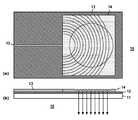
図1に、シリコン光導波路の中を伝播する信号光を外部に取り出す即ち出力したり、外部から信号光をその中に取り入れる即ち入力したりするグレーティング(回折格子)構造を設けた光デバイスの概要を示す。図1では、(a)に光デバイス10の上平面図を示し、(b)に光デバイス10の側断面図を示す。図1は、シリコン光導波路から信号光を外部に取り出す即ち出力する場合を示す。FIG. 1 shows an outline of an optical device provided with a grating (diffraction grating) structure for taking out or outputting signal light propagating through a silicon optical waveguide to outside or taking in signal light from outside. Indicates. 1A is a top plan view of the
光デバイス10では、シリコン基板11の上に酸化物層12が設けられ、酸化物層12の上にシリコン光導波路13が形成されている。さらに、シリコン光導波路13の一方の端にグレーティングカプラ14が形成されている。グレーティングカプラ14には、複数の溝が平行に同心円状に設けられている。グレーティングカプラ14での回折による回折光は、酸化物層12およびシリコン基板11を通って外部に出て行く。In the
特許文献1に、基板の上に設けられ光導波路からの信号光を基板の上方向に光路変換する集光型グレーティングカップラにおいて、回折格子部が、光導波路のコア層とは異なる、例えば上部クラッド層や別途形成した他の層に形成されていても良いことが示されている。Patent Document 1 discloses a concentrating grating coupler that is provided on a substrate and optically converts signal light from an optical waveguide in an upward direction of the substrate. The diffraction grating portion is different from the core layer of the optical waveguide. It is shown that it may be formed in a layer or another layer formed separately.
特許文献2に、光導波路層の一端に設けられたグレーティングを覆うオーバークラッド層の上に金などの光反射膜を形成することが示されている。Patent Document 2 discloses that a light reflecting film such as gold is formed on an over clad layer covering a grating provided at one end of an optical waveguide layer.
通常、シリコン光導波路の結合用回折格子は、光導波路のコア層と同じシリコン層を加工して形成される。しかしながら、コア層を直接加工すると、伝播モードへの影響が大きく、伝播損失が大きい。図1の光デバイス10のように、コア層を直接加工する回折格子では、回折格子の回折効率と結合効率は回折格子の加工深さだけで同時に決まるので、回折格子の設計および加工が簡単ではない。本発明は、回折格子の回折効率と結合効率を独立に決定できる光結合の実現を目的とする。本発明の目的には、そのような光結合を実現する光デバイスの提供が含まれる。Usually, the coupling diffraction grating of the silicon optical waveguide is formed by processing the same silicon layer as the core layer of the optical waveguide. However, when the core layer is directly processed, the influence on the propagation mode is large and the propagation loss is large. As in the
本発明により提供される1実施態様の光デバイスは、光導波路の一端を成す第1の層と、第1の層の上に第1の層よりも屈折率の低い第2の層を備え、第1の層から第2の層に入る光を回折させて第2の層から第1の層に出す光回折手段とを含む。An optical device of one embodiment provided by the present invention includes a first layer forming one end of an optical waveguide, and a second layer having a lower refractive index than the first layer on the first layer, Light diffracting means for diffracting light entering the second layer from the first layer and emitting the light from the second layer to the first layer.
好ましくは、光デバイスは、第1の層がシリコンから成り、第2の層が窒化シリコン、酸化シリコン又は酸化窒化シリコンから成ると良い。Preferably, in the optical device, the first layer is made of silicon, and the second layer is made of silicon nitride, silicon oxide, or silicon oxynitride.
好ましくは、光デバイスは、光回折手段が、第2の層の上に回折格子構造を成す第3の層を備えると良い。Preferably, in the optical device, the light diffracting means may include a third layer forming a diffraction grating structure on the second layer.
好ましくは、光デバイスは、第3の層の回折格子構造の上に反射膜を備えると良い。Preferably, the optical device includes a reflective film on the diffraction grating structure of the third layer.
好ましくは、光デバイスは、第2の層が回折格子構造を成すと良い。Preferably, in the optical device, the second layer has a diffraction grating structure.
好ましくは、光デバイスは、第2の層の回折格子構造の上に反射膜を備えると良い。Preferably, the optical device may include a reflective film on the diffraction grating structure of the second layer.
好ましくは、光デバイスは、反射膜が金属から成ると良い。Preferably, in the optical device, the reflective film is made of metal.
本発明により、回折格子の回折効率と結合効率を独立に決定できる光結合が実現される。特に、回折格子の回折効率と結合効率を独立に決定できるので、回折格子を作製する設計の自由度が増し、回折格子の回折効率を十分に高くした上で、回折格子への結合効率を独立に制御して、最適な回折格子を作製することができ、高い回折効率と結合効率を達成する。According to the present invention, optical coupling capable of independently determining the diffraction efficiency and the coupling efficiency of the diffraction grating is realized. In particular, since the diffraction efficiency and coupling efficiency of the diffraction grating can be determined independently, the degree of freedom in designing the diffraction grating is increased, the diffraction efficiency of the diffraction grating is sufficiently high, and the coupling efficiency to the diffraction grating is independent. The diffraction grating can be optimally controlled to achieve high diffraction efficiency and coupling efficiency.
以下、本発明を実施するための最良の形態を図面に基づいて詳細に説明するが、以下の実施形態は特許請求の範囲に係る発明を限定するものではなく、また実施形態の中で説明されている特徴の組み合わせの全てが発明の解決手段に必須であるとは限らない。本発明は多くの異なる態様で実施することが可能であり、記載された実施形態の内容に限定して解釈されるべきではない。なお、実施形態の説明の全体を通じて同じ構成部分乃至構成要素には同じ番号を付している。BEST MODE FOR CARRYING OUT THE INVENTION Hereinafter, the best mode for carrying out the present invention will be described in detail with reference to the drawings. However, the following embodiments do not limit the invention according to the claims, and are described in the embodiments. Not all combinations of features that are present are essential to the solution of the invention. The present invention may be implemented in many different ways and should not be construed as limited to the details of the described embodiments. Note that the same reference numerals are given to the same components or components throughout the description of the embodiment.
図2に、本発明の1実施形態に係る、光導波路の一端を成すコア層の上に屈折率の低い層と回折格子構造を成す層とを設けた光デバイス20を概略的に示す。図2でも、(a)に光デバイス20の上平面図を示し、(b)に光デバイス20の側断面図を示す。FIG. 2 schematically shows an
光デバイス20でも、光デバイス10と同様に、シリコン基板11の上に酸化物層12が設けられ、酸化物層12の上にシリコン光導波路13が形成されている。しかし、光デバイス20では、シリコン光導波路13の一端を成す、例えばシリコンの第1の層21に回折格子構造は設けられない。第1の層21の上には、第1の層21よりも屈折率の低い、好ましくは窒化シリコン、酸化シリコン又は酸化窒化シリコンから成る第2の層22が設けられる。そして、第2の層22の上に、例えばシリコンから成る第3の層23が設けられて、第3の層23に回折格子構造が形成される。In the
シリコン光導波路13の一端を成す第1の層21そのものには回折格子構造を形成しないで、第1の層21の上に低屈折率の第2の層22を設け、第2の層22の上に第3の層23を設けて、第3の層23に回折格子構造を形成するので、回折格子構造の作製が容易になる。また、シリコン光導波路13の一端を成す第1の層21そのものには回折格子構造を形成していないので、第1の層21では信号光の回折は起きず、信号光は第2の層22に導かれ、回折格子構造が形成されている第3の層23で信号光の回折が起きる。The
図3に、回折格子構造を成す第3の層23に反射膜31を設けた光デバイス30を概略的に示す。回折格子構造を成す第3の層23の上に反射膜31を設けることにより、第3の層23での回折光は、第2の層22がある下方向だけの一方向に限定されることになり、結合効率を高くすることができる。FIG. 3 schematically shows an
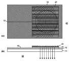
図4に、本発明の他の実施形態に係る、光導波路の一端を成すコア層の上に屈折率の低い層を設けて回折格子構造を形成した光デバイス40を概略的に示す。図4でも、(a)に光デバイス40の上平面図を示し、(b)に光デバイス40の側断面図を示す。FIG. 4 schematically shows an
光デバイス40でも、光デバイス10と同様に、シリコン基板11の上に酸化物層12が設けられ、酸化物層12の上にシリコン光導波路13が形成されている。しかし、光デバイス40でも、光デバイス20と同様に、シリコン光導波路13の一端を成す、例えばシリコンの第1の層21に回折格子構造は設けられない。第1の層21の上には、第1の層21よりも屈折率の低い、好ましくは窒化シリコン、酸化シリコン又は酸化窒化シリコンから成る第2の層41が設けられる。そして、この第2の層41に回折格子構造が形成される。In the
光デバイス40でも、シリコン光導波路13の一端を成す第1の層21そのものには回折格子構造を形成しないで、第1の層21の上に低屈折率の第2の層41を設け、第2の層41に回折格子構造を形成するので、回折格子構造の作製が容易になる。また、シリコン光導波路13の一端を成す第1の層21そのものには回折格子構造を形成していないので、第1の層21では信号光の回折は起きず、信号光は第2の層41に導かれ、回折格子構造が形成されている第2の層41で信号光の回折が起きる。Even in the
図5に、回折格子構造を成す第2の層41に反射膜51を設けた光デバイス50を概略的に示す。回折格子構造を成す第2の層41の上に反射膜51を設けることにより、第2の層41での回折光は、第1の層21がある下方向だけの一方向に限定されることになり、結合効率を高くすることができる。FIG. 5 schematically shows an
図2乃至図4では、シリコン光導波路13から信号光を外部に取り出す即ち出力する場合が示されているが、光デバイス20、30、40および50は、外部から信号光をシリコン光導波路13の中に取り入れる即ち入力する場合でも使用することができ、高い回折効率と結合効率を達成する。FIGS. 2 to 4 show the case where the signal light is extracted from the silicon
以上、実施態様を用いて本発明の説明をしたが、本発明の技術的範囲は実施態様について記載した範囲には限定されない。実施態様に種々の変更又は改良を加えることが可能であり、そのような変更又は改良を加えた態様も当然に本発明の技術的範囲に含まれる。As mentioned above, although this invention was demonstrated using the embodiment, the technical scope of this invention is not limited to the range described about the embodiment. Various modifications or improvements can be added to the embodiments, and the modes with such modifications or improvements are naturally included in the technical scope of the present invention.
10、20、30、40、50 光デバイス
21 第1の層
22、41 第2の層
23 第3の層
31、51 反射膜10, 20, 30, 40, 50
Claims (7)
Translated fromJapanese前記第1の層の上に前記第1の層よりも屈折率の低い第2の層を備え、前記第1の層から前記第2の層に入る光を回折させて前記第2の層から前記第1の層に出す光回折手段と、
を含む、光デバイス。A first layer forming one end of the optical waveguide;
A second layer having a lower refractive index than the first layer is provided on the first layer, and light entering the second layer from the first layer is diffracted to diffract light from the second layer. A light diffracting means for emitting to the first layer;
Including optical devices.
Priority Applications (2)
| Application Number | Priority Date | Filing Date | Title |
|---|---|---|---|
| JP2013136917AJP2015011207A (en) | 2013-06-28 | 2013-06-28 | Optical device |
| US14/299,354US9638864B2 (en) | 2013-06-28 | 2014-06-09 | Optical device |
Applications Claiming Priority (1)
| Application Number | Priority Date | Filing Date | Title |
|---|---|---|---|
| JP2013136917AJP2015011207A (en) | 2013-06-28 | 2013-06-28 | Optical device |
Publications (1)
| Publication Number | Publication Date |
|---|---|
| JP2015011207Atrue JP2015011207A (en) | 2015-01-19 |
Family
ID=52115678
Family Applications (1)
| Application Number | Title | Priority Date | Filing Date |
|---|---|---|---|
| JP2013136917APendingJP2015011207A (en) | 2013-06-28 | 2013-06-28 | Optical device |
Country Status (2)
| Country | Link |
|---|---|
| US (1) | US9638864B2 (en) |
| JP (1) | JP2015011207A (en) |
Families Citing this family (1)
| Publication number | Priority date | Publication date | Assignee | Title |
|---|---|---|---|---|
| CN114460745B (en)* | 2020-11-09 | 2024-06-07 | 宏达国际电子股份有限公司 | Waveguide device and optical engine |
Citations (5)
| Publication number | Priority date | Publication date | Assignee | Title |
|---|---|---|---|---|
| US5303316A (en)* | 1989-12-22 | 1994-04-12 | David Sarnoff Research Center, Inc. | Optical beam scanner |
| US20040156589A1 (en)* | 2003-02-11 | 2004-08-12 | Luxtera, Inc | Optical waveguide grating coupler incorporating reflective optical elements and anti-reflection elements |
| JP2010044290A (en)* | 2008-08-18 | 2010-02-25 | Oki Electric Ind Co Ltd | Diameter broadening circuit of optical waveguide, method of manufacturing the same and optical waveguide type apparatus |
| US20120045172A1 (en)* | 2010-08-23 | 2012-02-23 | Hon Hai Precision Industry Co., Ltd. | Grating coupler and package structure incorporating the same |
| JP2012098513A (en)* | 2010-11-02 | 2012-05-24 | Kyoto Institute Of Technology | Wavelength selection filter, and filter device and laser device provided with the same |
Family Cites Families (2)
| Publication number | Priority date | Publication date | Assignee | Title |
|---|---|---|---|---|
| JP2011107384A (en) | 2009-11-17 | 2011-06-02 | Nec Corp | Method for manufacturing optical coupling device |
| US9239432B2 (en)* | 2013-03-14 | 2016-01-19 | Micron Technology, Inc. | Photonics grating coupler and method of manufacture |
- 2013
- 2013-06-28JPJP2013136917Apatent/JP2015011207A/enactivePending
- 2014
- 2014-06-09USUS14/299,354patent/US9638864B2/enactiveActive
Patent Citations (5)
| Publication number | Priority date | Publication date | Assignee | Title |
|---|---|---|---|---|
| US5303316A (en)* | 1989-12-22 | 1994-04-12 | David Sarnoff Research Center, Inc. | Optical beam scanner |
| US20040156589A1 (en)* | 2003-02-11 | 2004-08-12 | Luxtera, Inc | Optical waveguide grating coupler incorporating reflective optical elements and anti-reflection elements |
| JP2010044290A (en)* | 2008-08-18 | 2010-02-25 | Oki Electric Ind Co Ltd | Diameter broadening circuit of optical waveguide, method of manufacturing the same and optical waveguide type apparatus |
| US20120045172A1 (en)* | 2010-08-23 | 2012-02-23 | Hon Hai Precision Industry Co., Ltd. | Grating coupler and package structure incorporating the same |
| JP2012098513A (en)* | 2010-11-02 | 2012-05-24 | Kyoto Institute Of Technology | Wavelength selection filter, and filter device and laser device provided with the same |
Also Published As
| Publication number | Publication date |
|---|---|
| US20150003781A1 (en) | 2015-01-01 |
| US9638864B2 (en) | 2017-05-02 |
Similar Documents
| Publication | Publication Date | Title |
|---|---|---|
| JP6175263B2 (en) | Spot size converter, manufacturing method thereof, and optical integrated circuit device | |
| WO2016131355A1 (en) | Photonic chip surface grating coupler (sgc) -based optical splitter and optical combiner | |
| WO2014034458A1 (en) | Structure for connecting optical module and optical connector | |
| JP6130290B2 (en) | Mode coupler | |
| JP2010524022A (en) | Multiplexer waveguide coupling method and system | |
| JP6402519B2 (en) | Optical waveguide device | |
| US9372312B2 (en) | Optical device | |
| US20180306977A1 (en) | Method And System For Mode Converters For Grating Couplers | |
| CN110770615A (en) | Method and system for two-dimensional pattern-matched grating coupler | |
| JP2016018191A (en) | Spot size converter and manufacturing method thereof | |
| CN109791251A (en) | Beam spot size converter | |
| JP2015011207A (en) | Optical device | |
| JP2017134228A (en) | Optical waveguide | |
| JP2010085564A (en) | Optical waveguide circuit and optical circuit device | |
| JP5104568B2 (en) | Light guide plate and optical module | |
| JP5263071B2 (en) | Optical interconnection circuit | |
| JP6302375B2 (en) | Optical receiver | |
| JP2013195721A (en) | Optical micro ring resonator | |
| JP2015191029A (en) | spot size converter | |
| JP6325941B2 (en) | Optical circuit | |
| JP6002795B1 (en) | Spot size converter | |
| JP5772436B2 (en) | Optical coupler and optical device | |
| JP4408083B2 (en) | Optical multiplexing / demultiplexing device and optical circuit using the same | |
| WO2013157287A1 (en) | Optical module | |
| JP2009080449A (en) | Wavelength multiplex optical coupler |
Legal Events
| Date | Code | Title | Description |
|---|---|---|---|
| A521 | Request for written amendment filed | Free format text:JAPANESE INTERMEDIATE CODE: A821 Effective date:20150626 | |
| RD12 | Notification of acceptance of power of sub attorney | Free format text:JAPANESE INTERMEDIATE CODE: A7432 Effective date:20150626 | |
| A521 | Request for written amendment filed | Free format text:JAPANESE INTERMEDIATE CODE: A821 Effective date:20150630 | |
| A521 | Request for written amendment filed | Free format text:JAPANESE INTERMEDIATE CODE: A821 Effective date:20160317 | |
| A621 | Written request for application examination | Free format text:JAPANESE INTERMEDIATE CODE: A621 Effective date:20160317 | |
| A977 | Report on retrieval | Free format text:JAPANESE INTERMEDIATE CODE: A971007 Effective date:20161207 | |
| A131 | Notification of reasons for refusal | Free format text:JAPANESE INTERMEDIATE CODE: A131 Effective date:20161228 | |
| A02 | Decision of refusal | Free format text:JAPANESE INTERMEDIATE CODE: A02 Effective date:20170816 |