JP2014522700A - Electrode, electrode system and manufacturing method thereof - Google Patents
Electrode, electrode system and manufacturing method thereofDownload PDFInfo
- Publication number
- JP2014522700A JP2014522700AJP2014521614AJP2014521614AJP2014522700AJP 2014522700 AJP2014522700 AJP 2014522700AJP 2014521614 AJP2014521614 AJP 2014521614AJP 2014521614 AJP2014521614 AJP 2014521614AJP 2014522700 AJP2014522700 AJP 2014522700A
- Authority
- JP
- Japan
- Prior art keywords
- conductive
- layer
- electrode
- conductive layer
- connector
- Prior art date
- Legal status (The legal status is an assumption and is not a legal conclusion. Google has not performed a legal analysis and makes no representation as to the accuracy of the status listed.)
- Granted
Links
- 238000004519manufacturing processMethods0.000titledescription14
- 230000000638stimulationEffects0.000claimsabstractdescription104
- 238000000034methodMethods0.000claimsabstractdescription63
- 230000001225therapeutic effectEffects0.000claimsdescription24
- 238000004891communicationMethods0.000claimsdescription22
- 239000000463materialSubstances0.000claimsdescription21
- 239000011248coating agentSubstances0.000claimsdescription19
- 238000000576coating methodMethods0.000claimsdescription19
- 150000001875compoundsChemical class0.000claimsdescription18
- 230000002093peripheral effectEffects0.000claimsdescription15
- 238000012377drug deliveryMethods0.000claimsdescription12
- 229910052782aluminiumInorganic materials0.000claimsdescription10
- XAGFODPZIPBFFR-UHFFFAOYSA-NaluminiumChemical compound[Al]XAGFODPZIPBFFR-UHFFFAOYSA-N0.000claimsdescription10
- OKTJSMMVPCPJKN-UHFFFAOYSA-NCarbonChemical group[C]OKTJSMMVPCPJKN-UHFFFAOYSA-N0.000claimsdescription8
- 229910052799carbonInorganic materials0.000claimsdescription8
- 238000003825pressingMethods0.000claimsdescription7
- 229920000642polymerPolymers0.000claimsdescription5
- 239000000126substanceSubstances0.000claimsdescription5
- 229910000859α-FeInorganic materials0.000claimsdescription4
- 238000002788crimpingMethods0.000claimsdescription3
- 229920002635polyurethanePolymers0.000claimsdescription3
- 239000004814polyurethaneSubstances0.000claimsdescription3
- 239000004800polyvinyl chlorideSubstances0.000claimsdescription3
- 229920000915polyvinyl chloridePolymers0.000claimsdescription3
- 229910001220stainless steelInorganic materials0.000claimsdescription3
- 239000010935stainless steelSubstances0.000claimsdescription3
- 230000005540biological transmissionEffects0.000claimsdescription2
- 239000006260foamSubstances0.000claimsdescription2
- 238000010438heat treatmentMethods0.000claimsdescription2
- 239000000499gelSubstances0.000description103
- 210000001519tissueAnatomy0.000description43
- 238000002646transcutaneous electrical nerve stimulationMethods0.000description23
- 239000004020conductorSubstances0.000description16
- 239000000853adhesiveSubstances0.000description11
- 230000001070adhesive effectEffects0.000description11
- WABPQHHGFIMREM-UHFFFAOYSA-Nlead(0)Chemical compound[Pb]WABPQHHGFIMREM-UHFFFAOYSA-N0.000description11
- 238000002560therapeutic procedureMethods0.000description10
- 238000007373indentationMethods0.000description9
- 230000008569processEffects0.000description7
- 238000010586diagramMethods0.000description6
- 238000009826distributionMethods0.000description6
- 229910052751metalInorganic materials0.000description6
- 239000002184metalSubstances0.000description6
- 238000012986modificationMethods0.000description6
- 230000004048modificationEffects0.000description6
- 238000013500data storageMethods0.000description5
- 230000032798delaminationEffects0.000description5
- 239000012811non-conductive materialSubstances0.000description5
- 229920003023plasticPolymers0.000description5
- 239000004033plasticSubstances0.000description5
- 238000012545processingMethods0.000description5
- 230000008901benefitEffects0.000description4
- 230000015572biosynthetic processEffects0.000description4
- 238000001827electrotherapyMethods0.000description4
- 230000006870functionEffects0.000description4
- 230000004888barrier functionEffects0.000description3
- 230000000295complement effectEffects0.000description3
- 229920001940conductive polymerPolymers0.000description3
- 230000000694effectsEffects0.000description3
- 150000002739metalsChemical class0.000description3
- 238000004080punchingMethods0.000description3
- 230000004044responseEffects0.000description3
- 239000000758substrateSubstances0.000description3
- HBBGRARXTFLTSG-UHFFFAOYSA-NLithium ionChemical compound[Li+]HBBGRARXTFLTSG-UHFFFAOYSA-N0.000description2
- 235000014676Phragmites communisNutrition0.000description2
- 230000008859changeEffects0.000description2
- 238000006243chemical reactionMethods0.000description2
- 210000000078clawAnatomy0.000description2
- 238000010276constructionMethods0.000description2
- 238000005260corrosionMethods0.000description2
- 230000007797corrosionEffects0.000description2
- 230000007423decreaseEffects0.000description2
- 238000013461designMethods0.000description2
- 238000005553drillingMethods0.000description2
- 230000005684electric fieldEffects0.000description2
- 239000012212insulatorSubstances0.000description2
- 230000001788irregularEffects0.000description2
- 229910001416lithium ionInorganic materials0.000description2
- 230000007246mechanismEffects0.000description2
- 238000012544monitoring processMethods0.000description2
- 229920001296polysiloxanePolymers0.000description2
- 230000003014reinforcing effectEffects0.000description2
- 238000005476solderingMethods0.000description2
- 238000006467substitution reactionMethods0.000description2
- 238000003856thermoformingMethods0.000description2
- 238000007666vacuum formingMethods0.000description2
- 241000282537Mandrillus sphinxSpecies0.000description1
- 206010049816Muscle tightnessDiseases0.000description1
- 208000012266Needlestick injuryDiseases0.000description1
- 229910052779NeodymiumInorganic materials0.000description1
- 206010040880Skin irritationDiseases0.000description1
- 238000009825accumulationMethods0.000description1
- 238000004026adhesive bondingMethods0.000description1
- 230000002917arthritic effectEffects0.000description1
- 230000000712assemblyEffects0.000description1
- 238000000429assemblyMethods0.000description1
- 230000033228biological regulationEffects0.000description1
- 230000002051biphasic effectEffects0.000description1
- 210000000988bone and boneAnatomy0.000description1
- 150000001793charged compoundsChemical class0.000description1
- 230000001427coherent effectEffects0.000description1
- 230000008878couplingEffects0.000description1
- 238000010168coupling processMethods0.000description1
- 238000005859coupling reactionMethods0.000description1
- 239000013078crystalSubstances0.000description1
- 238000005520cutting processMethods0.000description1
- 229920001971elastomerPolymers0.000description1
- 238000005516engineering processMethods0.000description1
- 238000009207exercise therapyMethods0.000description1
- 238000001914filtrationMethods0.000description1
- 239000012530fluidSubstances0.000description1
- 239000000017hydrogelSubstances0.000description1
- 230000007794irritationEffects0.000description1
- 238000002955isolationMethods0.000description1
- 238000005304joiningMethods0.000description1
- 210000003127kneeAnatomy0.000description1
- 238000003475laminationMethods0.000description1
- 239000007788liquidSubstances0.000description1
- 239000000696magnetic materialSubstances0.000description1
- 230000005389magnetismEffects0.000description1
- 238000007726management methodMethods0.000description1
- 239000011159matrix materialSubstances0.000description1
- 210000003205muscleAnatomy0.000description1
- QEFYFXOXNSNQGX-UHFFFAOYSA-Nneodymium atomChemical compound[Nd]QEFYFXOXNSNQGX-UHFFFAOYSA-N0.000description1
- 239000000615nonconductorSubstances0.000description1
- 238000002360preparation methodMethods0.000description1
- 230000008707rearrangementEffects0.000description1
- 230000002787reinforcementEffects0.000description1
- 239000011347resinSubstances0.000description1
- 229920005989resinPolymers0.000description1
- 238000007789sealingMethods0.000description1
- 230000035939shockEffects0.000description1
- 230000036556skin irritationEffects0.000description1
- 231100000475skin irritationToxicity0.000description1
- 238000009827uniform distributionMethods0.000description1
- 238000004804windingMethods0.000description1
- 210000000707wristAnatomy0.000description1
Images


Classifications
- A—HUMAN NECESSITIES
- A61—MEDICAL OR VETERINARY SCIENCE; HYGIENE
- A61N—ELECTROTHERAPY; MAGNETOTHERAPY; RADIATION THERAPY; ULTRASOUND THERAPY
- A61N1/00—Electrotherapy; Circuits therefor
- A61N1/02—Details
- A61N1/04—Electrodes
- A61N1/0404—Electrodes for external use
- A61N1/0408—Use-related aspects
- A61N1/0428—Specially adapted for iontophoresis, e.g. AC, DC or including drug reservoirs
- A61N1/0432—Anode and cathode
- A61N1/044—Shape of the electrode
- A—HUMAN NECESSITIES
- A61—MEDICAL OR VETERINARY SCIENCE; HYGIENE
- A61B—DIAGNOSIS; SURGERY; IDENTIFICATION
- A61B5/00—Measuring for diagnostic purposes; Identification of persons
- A61B5/24—Detecting, measuring or recording bioelectric or biomagnetic signals of the body or parts thereof
- A61B5/25—Bioelectric electrodes therefor
- A61B5/251—Means for maintaining electrode contact with the body
- A—HUMAN NECESSITIES
- A61—MEDICAL OR VETERINARY SCIENCE; HYGIENE
- A61B—DIAGNOSIS; SURGERY; IDENTIFICATION
- A61B5/00—Measuring for diagnostic purposes; Identification of persons
- A61B5/24—Detecting, measuring or recording bioelectric or biomagnetic signals of the body or parts thereof
- A61B5/25—Bioelectric electrodes therefor
- A61B5/263—Bioelectric electrodes therefor characterised by the electrode materials
- A61B5/268—Bioelectric electrodes therefor characterised by the electrode materials containing conductive polymers, e.g. PEDOT:PSS polymers
- A—HUMAN NECESSITIES
- A61—MEDICAL OR VETERINARY SCIENCE; HYGIENE
- A61B—DIAGNOSIS; SURGERY; IDENTIFICATION
- A61B5/00—Measuring for diagnostic purposes; Identification of persons
- A61B5/24—Detecting, measuring or recording bioelectric or biomagnetic signals of the body or parts thereof
- A61B5/25—Bioelectric electrodes therefor
- A61B5/271—Arrangements of electrodes with cords, cables or leads, e.g. single leads or patient cord assemblies
- A61B5/273—Connection of cords, cables or leads to electrodes
- A61B5/274—Connection of cords, cables or leads to electrodes using snap or button fasteners
- A—HUMAN NECESSITIES
- A61—MEDICAL OR VETERINARY SCIENCE; HYGIENE
- A61N—ELECTROTHERAPY; MAGNETOTHERAPY; RADIATION THERAPY; ULTRASOUND THERAPY
- A61N1/00—Electrotherapy; Circuits therefor
- A61N1/02—Details
- A61N1/04—Electrodes
- A61N1/0404—Electrodes for external use
- A61N1/0408—Use-related aspects
- A61N1/0428—Specially adapted for iontophoresis, e.g. AC, DC or including drug reservoirs
- A—HUMAN NECESSITIES
- A61—MEDICAL OR VETERINARY SCIENCE; HYGIENE
- A61N—ELECTROTHERAPY; MAGNETOTHERAPY; RADIATION THERAPY; ULTRASOUND THERAPY
- A61N1/00—Electrotherapy; Circuits therefor
- A61N1/02—Details
- A61N1/04—Electrodes
- A61N1/0404—Electrodes for external use
- A61N1/0408—Use-related aspects
- A61N1/0456—Specially adapted for transcutaneous electrical nerve stimulation [TENS]
- A—HUMAN NECESSITIES
- A61—MEDICAL OR VETERINARY SCIENCE; HYGIENE
- A61N—ELECTROTHERAPY; MAGNETOTHERAPY; RADIATION THERAPY; ULTRASOUND THERAPY
- A61N1/00—Electrotherapy; Circuits therefor
- A61N1/02—Details
- A61N1/04—Electrodes
- A61N1/0404—Electrodes for external use
- A61N1/0472—Structure-related aspects
- A61N1/048—Electrodes characterised by a specific connection between lead and electrode
- A—HUMAN NECESSITIES
- A61—MEDICAL OR VETERINARY SCIENCE; HYGIENE
- A61N—ELECTROTHERAPY; MAGNETOTHERAPY; RADIATION THERAPY; ULTRASOUND THERAPY
- A61N1/00—Electrotherapy; Circuits therefor
- A61N1/02—Details
- A61N1/04—Electrodes
- A61N1/0404—Electrodes for external use
- A61N1/0472—Structure-related aspects
- A61N1/0492—Patch electrodes
- A—HUMAN NECESSITIES
- A61—MEDICAL OR VETERINARY SCIENCE; HYGIENE
- A61N—ELECTROTHERAPY; MAGNETOTHERAPY; RADIATION THERAPY; ULTRASOUND THERAPY
- A61N1/00—Electrotherapy; Circuits therefor
- A61N1/18—Applying electric currents by contact electrodes
- A61N1/20—Applying electric currents by contact electrodes continuous direct currents
- A61N1/30—Apparatus for iontophoresis, i.e. transfer of media in ionic state by an electromotoric force into the body, or cataphoresis
- A—HUMAN NECESSITIES
- A61—MEDICAL OR VETERINARY SCIENCE; HYGIENE
- A61N—ELECTROTHERAPY; MAGNETOTHERAPY; RADIATION THERAPY; ULTRASOUND THERAPY
- A61N1/00—Electrotherapy; Circuits therefor
- A61N1/18—Applying electric currents by contact electrodes
- A61N1/32—Applying electric currents by contact electrodes alternating or intermittent currents
- A61N1/325—Applying electric currents by contact electrodes alternating or intermittent currents for iontophoresis, i.e. transfer of media in ionic state by an electromotoric force into the body
- A—HUMAN NECESSITIES
- A61—MEDICAL OR VETERINARY SCIENCE; HYGIENE
- A61N—ELECTROTHERAPY; MAGNETOTHERAPY; RADIATION THERAPY; ULTRASOUND THERAPY
- A61N1/00—Electrotherapy; Circuits therefor
- A61N1/18—Applying electric currents by contact electrodes
- A61N1/32—Applying electric currents by contact electrodes alternating or intermittent currents
- A61N1/36—Applying electric currents by contact electrodes alternating or intermittent currents for stimulation
- A61N1/36014—External stimulators, e.g. with patch electrodes
- A—HUMAN NECESSITIES
- A61—MEDICAL OR VETERINARY SCIENCE; HYGIENE
- A61B—DIAGNOSIS; SURGERY; IDENTIFICATION
- A61B2562/00—Details of sensors; Constructional details of sensor housings or probes; Accessories for sensors
- A61B2562/12—Manufacturing methods specially adapted for producing sensors for in-vivo measurements
- A61B2562/125—Manufacturing methods specially adapted for producing sensors for in-vivo measurements characterised by the manufacture of electrodes
- A—HUMAN NECESSITIES
- A61—MEDICAL OR VETERINARY SCIENCE; HYGIENE
- A61B—DIAGNOSIS; SURGERY; IDENTIFICATION
- A61B2562/00—Details of sensors; Constructional details of sensor housings or probes; Accessories for sensors
- A61B2562/22—Arrangements of medical sensors with cables or leads; Connectors or couplings specifically adapted for medical sensors
- A61B2562/225—Connectors or couplings
- A61B2562/227—Sensors with electrical connectors
- A—HUMAN NECESSITIES
- A61—MEDICAL OR VETERINARY SCIENCE; HYGIENE
- A61B—DIAGNOSIS; SURGERY; IDENTIFICATION
- A61B5/00—Measuring for diagnostic purposes; Identification of persons
- A61B5/24—Detecting, measuring or recording bioelectric or biomagnetic signals of the body or parts thereof
- A61B5/25—Bioelectric electrodes therefor
- A61B5/251—Means for maintaining electrode contact with the body
- A61B5/257—Means for maintaining electrode contact with the body using adhesive means, e.g. adhesive pads or tapes
- A61B5/259—Means for maintaining electrode contact with the body using adhesive means, e.g. adhesive pads or tapes using conductive adhesive means, e.g. gels
- A—HUMAN NECESSITIES
- A61—MEDICAL OR VETERINARY SCIENCE; HYGIENE
- A61B—DIAGNOSIS; SURGERY; IDENTIFICATION
- A61B5/00—Measuring for diagnostic purposes; Identification of persons
- A61B5/24—Detecting, measuring or recording bioelectric or biomagnetic signals of the body or parts thereof
- A61B5/25—Bioelectric electrodes therefor
- A61B5/279—Bioelectric electrodes therefor specially adapted for particular uses
- A61B5/28—Bioelectric electrodes therefor specially adapted for particular uses for electrocardiography [ECG]
- A61B5/282—Holders for multiple electrodes
- H—ELECTRICITY
- H01—ELECTRIC ELEMENTS
- H01R—ELECTRICALLY-CONDUCTIVE CONNECTIONS; STRUCTURAL ASSOCIATIONS OF A PLURALITY OF MUTUALLY-INSULATED ELECTRICAL CONNECTING ELEMENTS; COUPLING DEVICES; CURRENT COLLECTORS
- H01R11/00—Individual connecting elements providing two or more spaced connecting locations for conductive members which are, or may be, thereby interconnected, e.g. end pieces for wires or cables supported by the wire or cable and having means for facilitating electrical connection to some other wire, terminal, or conductive member, blocks of binding posts
- H01R11/11—End pieces or tapping pieces for wires, supported by the wire and for facilitating electrical connection to some other wire, terminal or conductive member
- H01R11/30—End pieces held in contact by a magnet
- H—ELECTRICITY
- H01—ELECTRIC ELEMENTS
- H01R—ELECTRICALLY-CONDUCTIVE CONNECTIONS; STRUCTURAL ASSOCIATIONS OF A PLURALITY OF MUTUALLY-INSULATED ELECTRICAL CONNECTING ELEMENTS; COUPLING DEVICES; CURRENT COLLECTORS
- H01R2201/00—Connectors or connections adapted for particular applications
- H01R2201/12—Connectors or connections adapted for particular applications for medicine and surgery
- Y—GENERAL TAGGING OF NEW TECHNOLOGICAL DEVELOPMENTS; GENERAL TAGGING OF CROSS-SECTIONAL TECHNOLOGIES SPANNING OVER SEVERAL SECTIONS OF THE IPC; TECHNICAL SUBJECTS COVERED BY FORMER USPC CROSS-REFERENCE ART COLLECTIONS [XRACs] AND DIGESTS
- Y10—TECHNICAL SUBJECTS COVERED BY FORMER USPC
- Y10T—TECHNICAL SUBJECTS COVERED BY FORMER US CLASSIFICATION
- Y10T29/00—Metal working
- Y10T29/49—Method of mechanical manufacture
- Y10T29/49002—Electrical device making
- Y10T29/49117—Conductor or circuit manufacturing
- Y10T29/49124—On flat or curved insulated base, e.g., printed circuit, etc.
- Y10T29/49155—Manufacturing circuit on or in base
Landscapes
- Health & Medical Sciences (AREA)
- Life Sciences & Earth Sciences (AREA)
- Engineering & Computer Science (AREA)
- General Health & Medical Sciences (AREA)
- Veterinary Medicine (AREA)
- Biomedical Technology (AREA)
- Public Health (AREA)
- Animal Behavior & Ethology (AREA)
- Nuclear Medicine, Radiotherapy & Molecular Imaging (AREA)
- Radiology & Medical Imaging (AREA)
- Biophysics (AREA)
- Heart & Thoracic Surgery (AREA)
- Bioinformatics & Cheminformatics (AREA)
- Physics & Mathematics (AREA)
- Pathology (AREA)
- Medical Informatics (AREA)
- Molecular Biology (AREA)
- Surgery (AREA)
- Electrotherapy Devices (AREA)
Abstract
Translated fromJapaneseDescription
Translated fromJapanese[関連出願の相互参照]
本願は、2011年7月18日出願の米国仮出願第61/508874号の優先権を主張し、その全内容は参照として本願に組み込まれる。[Cross-reference of related applications]
This application claims priority from US Provisional Application No. 61/508874, filed July 18, 2011, the entire contents of which are incorporated herein by reference.
医療用の従来の電極には複数の欠点がある。第一に、或る電極は手作業で製造されていて、多重ストランドワイヤの一方の端のストランドを手で解いて、各ストランドをカーボンを含浸させた導電性ポリマーに対して扇状に広げて(fanning)、電極及びピグテールを形成する。別個のコネクタを多重ストランドワイヤの他方の端に取り付けるが、これは手ではんだ付けすることによって行われることが多い。電極のピグテールとして多重ストランドワイヤを用いると、ワイヤと導電性ポリマーとの間の複数の離散的な接触点が生じて、その各接触点が、電極表面における均一な電流分布を乱して、電気刺激治療中の患者を焼いてしまう可能性のある“ホットスポット”を形成し得る。ワイヤのストランド間の接触の不均一性もホットスポットの危険性を高め得る。このような電極は、目的とするカスタマイズされた治療を提供するために医者や患者が望む形状に切断したり容易に製造したりすることができないものである。或る電極はピグテールの代わりにスナップコネクタを含みが、これにもホットスポットの危険性があり、電気刺激リードへの接続及び接続解除が難しいものとなり得る。 Conventional electrodes for medical use have several drawbacks. First, some electrodes are manufactured by hand, the strands at one end of the multi-strand wire are manually unwound and each strand is fanned out against a conductive polymer impregnated with carbon ( fanning), forming electrodes and pigtails. A separate connector is attached to the other end of the multi-strand wire, often by hand soldering. Using a multi-strand wire as the electrode pigtail creates multiple discrete contact points between the wire and the conductive polymer, each of which disrupts the uniform current distribution on the electrode surface, “Hot spots” can be formed that can burn the patient undergoing stimulation treatment. Non-uniformity of contact between strands of wire can also increase the risk of hot spots. Such electrodes cannot be cut or easily manufactured into the shape desired by the physician or patient to provide the desired customized treatment. Some electrodes include snap connectors instead of pigtails, which also have the risk of hot spots and can be difficult to connect and disconnect to the electrical stimulation leads.
本願では、電極、電極コネクタ、刺激システム、及びそれらを組み立てる方法が開示される。一側面では、電極が提供される。特定の実施形態では、電極は、患者組織に治療電気刺激を印加するように設計された第一の領域と、第一の領域の単一延長部として構成されたテールを含む第二の領域とを有する導電性層を含む。一部実施形態では、導電性層はアルミニウム製である。コネクタが、テールの遠位端に配置されて、非導電性頂部層が導電性層の頂部に沿って配置される。一部実施形態では、テールの遠位端の先端が張り出している。張り出した先端は、雄型ピンを受容するように構成された内部通路を備えたチューブを形成し得る。一部実施形態では、コネクタは、波状レセプタクルを備えたコネクタ筐体を含む。テールの遠位端は、波状レセプタクルの導電性接続部に接続し得る。一部実施形態では、テールの遠位端は、電気刺激発生器からのリードと結合するように構成されたコネクタに対して波形に縮められるか又は接着される。 In this application, electrodes, electrode connectors, stimulation systems, and methods of assembling them are disclosed. In one aspect, an electrode is provided. In certain embodiments, the electrode includes a first region designed to apply therapeutic electrical stimulation to patient tissue and a second region including a tail configured as a single extension of the first region; A conductive layer having In some embodiments, the conductive layer is made of aluminum. A connector is disposed at the distal end of the tail and a non-conductive top layer is disposed along the top of the conductive layer. In some embodiments, the tip of the distal end of the tail overhangs. The overhanging tip may form a tube with an internal passage configured to receive a male pin. In some embodiments, the connector includes a connector housing with a corrugated receptacle. The distal end of the tail may be connected to the conductive connection of the wavy receptacle. In some embodiments, the distal end of the tail is crimped or glued to a connector configured to couple with a lead from the electrical stimulus generator.
一部実施形態では、第二の導電性層が単一テールの遠位端の上に配置される。第二の導電性層と、単一テールの遠位端とは、電気刺激リードからの雄型ピンを受容するように構成された内部通路を備えたチューブ内に形成され得る。第二の導電性層は、例えば、カーボンストリップ、又は、カーボンを含浸させた導電性のポリ塩化ビニルやポリウレタンであり得る。 In some embodiments, a second conductive layer is disposed on the distal end of the single tail. The second conductive layer and the distal end of the single tail can be formed in a tube with an internal passage configured to receive a male pin from the electrical stimulation lead. The second conductive layer can be, for example, a carbon strip or conductive polyvinyl chloride or polyurethane impregnated with carbon.
一部実施形態では、電極は、導電性層の下に配置されたゲル層を含む。一部実施形態では、電極は、導電性層のテールの底部に沿って配置された非導電性底部層を含む。非導電性底部層は、導電性層の下に部分的に配置された延長部を含み得る。また、底部層の延長部は、ゲル層の下にも部分的に配置され得る。一部実施形態では、導電性層は、周囲側面と、その周囲側面のまわりに少なくとも部分的に配置されたゲルコーティングとを有する。ゲルコーティングは、周囲側面全体に延在し得る。 In some embodiments, the electrode includes a gel layer disposed below the conductive layer. In some embodiments, the electrode includes a non-conductive bottom layer disposed along the bottom of the tail of the conductive layer. The non-conductive bottom layer may include an extension that is partially disposed below the conductive layer. An extension of the bottom layer can also be partially disposed under the gel layer. In some embodiments, the conductive layer has a peripheral side and a gel coating disposed at least partially around the peripheral side. The gel coating can extend over the entire peripheral side.
特定の実施形態では、電極は、非導電性頂部層と、非導電性頂部層の下に配置された導電性層と、導電性層の下に配置されたゲル層と、スナップコネクタとを含む。スナップコネクタは、非導電性頂部層の上に配置された第一の導電性筐体と、導電性層の下に配置された第二の筐体とを含み、その第二の筐体は、少なくとも部分的に非導電性であり、前記第一の導電性筐体に接続して導電性層及び非導電性頂部層に渡されるように構成される。一部実施形態では、第二の筐体は、非導電性素子と第一の導電性筐体との間に配置された第二の導電性筐体を含み、第二の導電性筐体は導電性層の下に配置される。非導電性素子はポリマーであり得る。一部実施形態では、導電性層は、周囲側面と、その周囲側面のまわりに少なくとも部分的に配置されたゲルコーティングとを有する。ゲルコーティングは周囲側面全体に延在し得る。 In certain embodiments, the electrode includes a non-conductive top layer, a conductive layer disposed under the non-conductive top layer, a gel layer disposed under the conductive layer, and a snap connector. . The snap connector includes a first conductive housing disposed over the non-conductive top layer and a second housing disposed under the conductive layer, the second housing comprising: At least partially non-conductive and configured to connect to the first conductive housing and to be passed to the conductive layer and the non-conductive top layer. In some embodiments, the second housing includes a second conductive housing disposed between the non-conductive element and the first conductive housing, wherein the second conductive housing is Located under the conductive layer. The non-conductive element can be a polymer. In some embodiments, the conductive layer has a peripheral side and a gel coating disposed at least partially around the peripheral side. The gel coating can extend over the entire peripheral side.
一部実施形態では、電極は、導電性層と、導電性層の頂部に沿って配置された導電性磁性層と、導電性磁性層の頂部に沿って配置された非導電性頂部層と、非導電性頂部層の頂部に沿って配置されて、磁気リードコネクタを受容するように構成されたソケットとを含む。一部実施形態では、導電性層はアルミニウムである。一部実施形態では、導電性磁性層は、ステンレス鋼等のフェライト材料を含む。一部実施形態では、導電性磁性層の直径は、導電性層の直径よりも小さい。一部実施形態では、ソケットは、ベース直径を有するベース部と、頂部直径を有する頂部とを有し、ベース直径が頂部直径よりも大きい。ベース部は非導電性頂部層の下に配置され得て、頂部は非導電性頂部層の上に配置され得る。 In some embodiments, the electrode comprises a conductive layer, a conductive magnetic layer disposed along the top of the conductive layer, a non-conductive top layer disposed along the top of the conductive magnetic layer, A socket disposed along the top of the non-conductive top layer and configured to receive a magnetic lead connector. In some embodiments, the conductive layer is aluminum. In some embodiments, the conductive magnetic layer includes a ferrite material such as stainless steel. In some embodiments, the diameter of the conductive magnetic layer is smaller than the diameter of the conductive layer. In some embodiments, the socket has a base portion having a base diameter and a top portion having a top diameter, the base diameter being greater than the top diameter. The base can be disposed below the non-conductive top layer, and the top can be disposed above the non-conductive top layer.
一部実施形態では、電極は、非導電性頂部層と、非導電性頂部層の下に配置された導電性層と、導電性層の下に配置されたゲル層と、電気刺激システムからのリードの雄型コネクタを受容するように構成された導電性層のくぼみとして構造化されたレセプタクルとを含む。非導電性素子がレセプタクルの下に配置される。一部実施形態では、レセプタクルは、雄型スナップコネクタを受容するように構成される。一部実施形態では、非導電性素子は、レセプタクルの底面とゲル層の底面との間に配置される。 In some embodiments, the electrode comprises a non-conductive top layer, a conductive layer disposed under the non-conductive top layer, a gel layer disposed under the conductive layer, and an electrical stimulation system. And a receptacle structured as a recess in the conductive layer configured to receive the male connector of the lead. A non-conductive element is disposed under the receptacle. In some embodiments, the receptacle is configured to receive a male snap connector. In some embodiments, the non-conductive element is disposed between the bottom surface of the receptacle and the bottom surface of the gel layer.
他の側面では、電極システムが提供される。特定の実施形態では、電極システムは、複数の導電性領域を含み、各導電性領域が、単一テールを備えた導電性層を有する電極を含む。また、電極システムは、複数のコネクタと、導電性領域の上に配置された非導電性頂部層とも含み、各コネクタが各単一テールの遠位端に配置される。複数の導電性領域は、絶縁発泡層によって横方向に分離され得る。一部実施形態では、複数の導電性領域が、非導電性頂部層のホールのまわりに対称に配置される。複数の導電性領域は、非導電性頂部層のホールのまわりに同心円状に配置され得る。一部実施形態では、複数の導電性領域のうちの第一の導電性領域が、複数の導電性領域のうちの第二の導電性領域と非導電性との間に配置される。また、非導電性層が、複数の導電性領域のうちの第一の導電性領域の一部と複数の導電性領域のうちの第二の導電性領域との間に配置され得る。 In another aspect, an electrode system is provided. In certain embodiments, the electrode system includes a plurality of conductive regions, each conductive region including an electrode having a conductive layer with a single tail. The electrode system also includes a plurality of connectors and a non-conductive top layer disposed over the conductive region, with each connector disposed at the distal end of each single tail. The plurality of conductive regions can be separated laterally by an insulating foam layer. In some embodiments, the plurality of conductive regions are arranged symmetrically around the holes in the non-conductive top layer. The plurality of conductive regions may be concentrically arranged around the holes of the nonconductive top layer. In some embodiments, the first conductive region of the plurality of conductive regions is disposed between the second conductive region of the plurality of conductive regions and non-conductive. In addition, the non-conductive layer may be disposed between a part of the first conductive region of the plurality of conductive regions and the second conductive region of the plurality of conductive regions.
特定の実施形態では、電極システムが、磁気リードコネクタを受容するように構成されたソケットと、磁気リードコネクタを含むリードとを有する電極を含み得て、その磁気リードコネクタは、ソケット内部に収容されるように構成された磁石を含む。磁気リードコネクタは外壁を含み得て、その外壁は、外壁と磁石との間にソケットの少なくとも一部を捕獲するように構成される。 In certain embodiments, the electrode system can include an electrode having a socket configured to receive a magnetic lead connector and a lead including the magnetic lead connector, the magnetic lead connector being housed within the socket. Including a magnet configured to. The magnetic lead connector may include an outer wall that is configured to capture at least a portion of the socket between the outer wall and the magnet.
本願で説明される電極及び電極システムの一部実施形態では、非導電性層が、非動径対称形状に形成される。非動径対称形状は矩形であり得る。本願で説明される電極及び電極システムの一部実施形態では、非導電性層が非対称形状に形成される。 In some embodiments of the electrodes and electrode systems described herein, the non-conductive layer is formed in a non-radial symmetric shape. The non-radial symmetric shape can be rectangular. In some embodiments of the electrodes and electrode systems described herein, the non-conductive layer is formed in an asymmetric shape.
他の側面では、刺激システムが提供される。特定の実施形態では、刺激システムは、非導電性頂部層と、非導電性頂部層の下に配置された電子機器層とを含む。電子機器層は、電子機器層の第一の導電性接触点と電気通信するパルス発生回路を含む。また、刺激システムは、電子機器層の下に配置された導電性層も含み、その導電性層は、電子機器層と導電性層との間の穴開け接続を介して第一の導電性接触点と電気的に接触して整列した第二の導電性接触点を有する。一部実施形態では、刺激システムは、電子機器層の下に配置された第二の導電性層を含む。第二の導電性層は、電子機器層と第二の導電性層との間の穴開け接続を介して電子機器層の第四の導電性接触点と電気的に接触して整列した第三の導電性接触点を有する。刺激システムは、本願で説明される電極又は電極システムのいずれかを含み得る。 In another aspect, a stimulation system is provided. In certain embodiments, the stimulation system includes a non-conductive top layer and an electronics layer disposed below the non-conductive top layer. The electronic device layer includes a pulse generation circuit that is in electrical communication with the first conductive contact point of the electronic device layer. The stimulation system also includes a conductive layer disposed below the electronic device layer, the conductive layer being a first conductive contact via a piercing connection between the electronic device layer and the conductive layer. A second conductive contact point is in electrical contact with the point and aligned. In some embodiments, the stimulation system includes a second conductive layer disposed below the electronics layer. The second conductive layer is aligned in electrical contact with the fourth conductive contact point of the electronic device layer via a piercing connection between the electronic device layer and the second conductive layer. With conductive contact points. The stimulation system can include any of the electrodes or electrode systems described herein.
他の側面では、イオン導入デリバリーシステムが提供される。特定の実施形態では、イオン導入デリバリーシステムは、導電性層と、ドラッグデリバリー層とを含む。ドラッグデリバリー層は、治療化合物を含み、DC(直流)電流が導電性層から患者組織に流れた際に患者組織内に治療化合物を届けるように配置される。また、イオン導入デリバリーシステムは、パルス発生回路を備えた電子機器層も含む。パルス発生回路は、所定の期間にわたって導電性層にDC電流を流して、患者組織内に治療化合物を届け、所定の期間にわたってDC電流を流した後に、導電性層にAC(交流)TENS電流を流すように構成される。一部実施形態では、イオン導入デリバリーシステムはバッテリも含み、パルス発生回路が、バッテリを用いてDC電流及びAC TENS電流を流すように構成される。一部実施形態では、イオン導入デリバリーシステムは、所定の量の治療化合物が患者組織内に届けられた際に所定の期間が経過したことを示すように構成された化学スイッチを含む。 In another aspect, an iontophoretic delivery system is provided. In certain embodiments, the iontophoretic delivery system includes a conductive layer and a drug delivery layer. The drug delivery layer includes a therapeutic compound and is arranged to deliver the therapeutic compound into the patient tissue when a DC (direct current) current flows from the conductive layer to the patient tissue. The iontophoretic delivery system also includes an electronic device layer that includes a pulse generation circuit. The pulse generation circuit applies a DC current to the conductive layer for a predetermined period of time to deliver the therapeutic compound into the patient tissue, and after applying the DC current for a predetermined period of time, an AC (alternating current) TENS current is applied to the conductive layer. Configured to flow. In some embodiments, the iontophoretic delivery system also includes a battery, and the pulse generation circuit is configured to flow DC current and AC TENS current using the battery. In some embodiments, the iontophoretic delivery system includes a chemical switch configured to indicate that a predetermined period of time has elapsed when a predetermined amount of therapeutic compound is delivered into the patient tissue.
他の側面では、電極を組み立てる方法が提供される。特定の実施形態では、本方法は、患者組織に治療電気刺激を印加するように設計された第一の領域と、第一の領域の単一延長部として構成されたテールを含む第二の領域とを含む導電性層を提供するステップと、導電性層の頂部に沿って非導電性頂部層を配置するステップと、テールの遠位端にコネクタを形成するステップとを含む。テールの遠位端にコネクタを形成するステップは、レセプタクル内にテールの遠位端を挿入することと、レセプタクル内部にテールの遠位端を固定するようにレセプタクルを波形に縮れさせることとを含み得る。テールの遠位端は、第一の側部及び第二の側部を備えた張り出し部を含み得て、この場合、コネクタを形成するステップは、第一の側部及び第二の側部を互いに近付けて固定して、張り出し部からチューブを形成することを含み得る。その固定は、第一の側部及び第二の側部を互いに近付けて配置することと、第一の側部及び第二の側部を互いに近付けた際に張り出し部のまわりに或る長さの熱収縮チューブを配置することと、熱収縮チューブを加熱して、張り出し部のまわりで熱収縮チューブの直径を減少させることによって、張り出し部をチューブ状に捕獲することとを含み得る。 In another aspect, a method for assembling an electrode is provided. In certain embodiments, the method includes a first region designed to apply therapeutic electrical stimulation to patient tissue and a second region including a tail configured as a single extension of the first region. Providing a conductive layer including: disposing a non-conductive top layer along the top of the conductive layer; and forming a connector at the distal end of the tail. Forming the connector at the distal end of the tail includes inserting the distal end of the tail into the receptacle and crimping the receptacle to corrugate to secure the distal end of the tail within the receptacle. obtain. The distal end of the tail can include an overhang with a first side and a second side, wherein the step of forming a connector includes the first side and the second side. It may include fixing the tube close together and forming a tube from the overhang. The fixing is such that the first side and the second side are arranged close to each other and a certain length around the overhang when the first side and the second side are brought close to each other. Placing the heat shrink tube and capturing the bulge in a tube by heating the heat shrink tube to reduce the diameter of the heat shrink tube around the bulge.
他の側面では、電極を組み立てる方法が提供される。特定の実施形態では、本方法は、導電性層を提供するステップと、導電性層の頂面にくぼみを形成するステップ(くぼみは電気刺激システムからのリードの雄型コネクタを受容するためのレセプタクルとして構成される)と、導電性層の底面にゲル層を配置するステップとを含む。一部実施形態では、本方法は、導電性層の底面とゲル層の底面との間において、くぼみの下に非導電性素子を配置するステップも含む。 In another aspect, a method for assembling an electrode is provided. In certain embodiments, the method includes providing a conductive layer and forming a recess in the top surface of the conductive layer (the recess is a receptacle for receiving a male connector of a lead from the electrical stimulation system). And a step of disposing a gel layer on the bottom surface of the conductive layer. In some embodiments, the method also includes disposing a non-conductive element below the recess between the bottom surface of the conductive layer and the bottom surface of the gel layer.
特定の側面では、電極システムを組み立てる方法が提供される。特定の実施形態では、本方法は、第一のリング状導電性層を提供するステップと、第一のリング状導電性層の内部にリング状導電性層を配置するステップと、リング状導電性層の内部に第二の導電性層を配置するステップと、第一及び第二のリング状導電性層の頂部に沿って非導電性頂部層を配置するステップとを含む。第二の導電性層はリング状であり得る。 In certain aspects, a method for assembling an electrode system is provided. In certain embodiments, the method includes providing a first ring-shaped conductive layer, placing the ring-shaped conductive layer within the first ring-shaped conductive layer, and ring-shaped conductive Disposing a second conductive layer within the layer; and disposing a non-conductive top layer along the top of the first and second ring-shaped conductive layers. The second conductive layer can be ring-shaped.
他の側面では、刺激システムを組み立てる方法が提供される。特定の実施形態では、本方法は、電子機器層の第一の導電性接触点と電気通信するパルス発生回路を含む電子機器層を提供するステップと、電子機器層の下に導電性層を配置するステップと、第一の導電性接触点において電子機器層及び導電性層に穴を開けて、電子機器層の導電性接触点と導電性層との間の電気接続を形成するステップとを含む。一部実施形態では、本方法は、導電性層の下にゲル層を配置するステップと、電子機器層の上に非導電性頂部層を配置するステップとを更に含む。一部実施形態では、電子機器層は、パルス発生回路を制御するように構成された一つ以上のスイッチを含み、本方法が、一つ以上のスイッチと整列した一つ以上のボタンを含み、一つ以上のボタンを押すと対応する一つ以上のスイッチが作動するようにするステップを更に含む。一部実施形態では、一つ以上のスイッチは電源オンスイッチを含み、電源オンスイッチに付随するボタンを押すと、パルス発生回路から導電性層に電気パルスを伝えることが開始する。 In another aspect, a method for assembling a stimulation system is provided. In certain embodiments, the method includes providing an electronic device layer that includes a pulse generating circuit that is in electrical communication with the first conductive contact point of the electronic device layer, and disposing the conductive layer below the electronic device layer. And piercing the electronic device layer and the conductive layer at a first conductive contact point to form an electrical connection between the conductive contact point of the electronic device layer and the conductive layer. . In some embodiments, the method further includes disposing a gel layer under the conductive layer and disposing a non-conductive top layer over the electronics layer. In some embodiments, the electronics layer includes one or more switches configured to control the pulse generation circuit, and the method includes one or more buttons aligned with the one or more switches, The method further includes causing one or more corresponding switches to be activated when one or more buttons are pressed. In some embodiments, the one or more switches include a power-on switch, and pressing a button associated with the power-on switch initiates an electrical pulse from the pulse generation circuit to the conductive layer.
他の側面では、イオン導入処置及びTENS処置を実施するための単一デバイスを構成する方法が提供される。特定の実施形態では、本方法は、導電性層と、治療化合物を備えたドラッグデリバリー層と、パルス発生回路とを有する電気刺激システムを提供するステップを含む。本方法は、患者組織の上に配置されて作動した際に、所定の期間にわたって導電性層のDC電流を流して、ドラッグデリバリー層から患者組織内に治療化合物を届けて、所定の期間にわたってDC電流を流した後に、AC TENS電流を導電性層に流すようにパルス発生回路を構成するステップを含み得る。一部実施形態では、本方法は、バッテリが枯渇するまでAC TENS電流を流すようにパルス発生回路を構成するステップを更に含む。 In another aspect, a method is provided for configuring a single device for performing iontophoresis and TENS procedures. In certain embodiments, the method includes providing an electrical stimulation system having a conductive layer, a drug delivery layer with a therapeutic compound, and a pulse generating circuit. When the method is placed and operated over patient tissue, the method applies a DC current in the conductive layer for a predetermined period of time to deliver the therapeutic compound from the drug delivery layer into the patient tissue and DC for a predetermined period of time. The method may include configuring the pulse generation circuit to flow an AC TENS current through the conductive layer after passing the current. In some embodiments, the method further includes configuring the pulse generator circuit to conduct AC TENS current until the battery is depleted.
本開示を読んだ後においては、当業者には多様なバリエーション及び修正が想起されるものであり、開示される特徴を、本願で開示される一以上の他の特徴との任意の組み合わせ及びサブコンビネーションで実施し得る(多数の従属項の組み合わせ及びサブコンビネーション等)。上記で説明又は例示した多様な特徴(その構成要素を含む)は、他のシステムと組み合わせたり統合したりすることができるものであり、更には、特定の特徴を省略したり実施しなかったりし得る。 After reading this disclosure, various variations and modifications will occur to those skilled in the art, and the disclosed features may be combined with any combination and sub-configuration with one or more other features disclosed herein. Can be implemented in combinations (such as combinations of subordinate claims and subcombinations). The various features described or exemplified above (including their components) can be combined or integrated with other systems, and certain features may be omitted or not implemented. obtain.
変更例、置換例及び修正例は、本願で開示される情報の範囲を逸脱せずに当業者には実施可能なものである。本願でひかれる全ての参考文献は、その全体が参照として本願に組み込まれ、本願の一部を成すものである。 Modifications, substitutions, and modifications can be made by those skilled in the art without departing from the scope of information disclosed herein. All references cited in this application are incorporated herein by reference in their entirety and form part of this application.
上述の及び他の課題及び利点は、添付図面を参照して、以下の説明からより完全に明らかとなるものである。 The above and other problems and advantages will become more fully apparent from the following description with reference to the accompanying drawings.
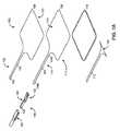
図1Aは一体(ユニボディ)電極100の分解図である。電極100は、非導電性頂部層106と、導電性層102と、ゲル層118と、非導電性底部層112とを含む。導電性層102は、本体117と、遠位端104a及び近位端104bを有する単一(ユニタリ)テール104とを含む。近位端104bは本体117内に延伸し、遠位端104aは、コネクタ108に含まれるコネクタ筐体120の波状レセプタクル122内部に収容される。コネクタ筐体120の遠位端128は、電気刺激デバイス(図示せず)からのリードと結合するように構成されて、導電性層102を電気刺激デバイスに結合して、電気刺激デバイスが発生させる電気刺激電流を、電極100を介して患者の組織に印加することができるようになっている。また、コネクタ108は、コネクタ筐体120に適合するコネクタジャケット126も含む。 FIG. 1A is an exploded view of an integral (unibody)
非導電性頂部層106は、導電性層102の頂部114に沿って配置される。非導電性頂部層106は、PTE等の非導電性シート材料製であり得て、その底面107に接着剤を含み、その接着剤は、非導電性頂部層106を導電性層102に接着するのに用いられる。非導電性頂部層106の寸法は、導電性層102の寸法と略同一の広がりを持つものであるが、非導電性頂部層106のテール105は、導電性層102のテール104よりも短くなり得て、電極100を組み立てた際に、テール105が、テール104と波状レセプタクルとの間に介在しないようにする(図2Bに示されるように)。 A non-conductive top layer 106 is disposed along the top 114 of the
導電性層102及びその単一テール104は好ましくはアルミニウムの連続片から形成されるが、他の金属や導電性プラスチック(例えば、カーボンを含浸させたポリマー)等の他の導体を用いてもよい。導電性層102及びその単一テール104は、例えば、導電材料のシートを打ち抜くことによって形成され得る。多重ストランドワイヤ製のピグテールを有する従来の電極とは異なり、単一テール104は導電性層102の本体117と連続している。この構成は、テール104と本体117との間の不規則な接続をなくして、導電性表面まわりに更に均一に電流を分布させるのに役立つ。この均一な分布は、導電性表面に不規則性を生じる可能性のあるホットスポットの形成を防止するのに役立ち、二種類の異種金属を接合する際に生じる腐食を回避する。また、導電性層102の単一テール104と本体117との間のインターフェースの引っ張り強度が、ストランドを扇状に広げることや多様な層の接着の質や均一性に依存する必要がなくなり、所定の製造バッチにおける電極間の機械特性がより一定になる。
ゲル層118は導電性層102の下に配置される。導電性ハイドロゲル等の多様なゲルをゲル層118に用いることができる。しかしながら、アルミニウム等の導電性層102に適した一部の導電性材料は、ゲル層118に用いられる一般的に利用可能なゲルに対して容易に接着しない可能性がある。導電性層102とゲル層118との間の接着強度が十分ではない場合、使用中に導電性層102がゲル層118から剥離し得る(例えば、使用前に、ゲル層118を保護する裏張り(ライナ)材料から電極100を剥がす場合や、電極100を患者組織から取り外す場合)。剥離は患者及び医師にとって不都合なものであり、導電性層102とゲル層118との間の不均一な接触を生じさせることが多く、電気刺激中における患者組織にわたる電流の不均一性が生じて、患者を焼いたり、所望の治療領域を刺激するのに失敗したりし得る。アルミニウム導電性層102を用いた際に剥離が生じる可能性を低減する一方法は、ゲルの化学的性質を変更して、導電性層102とゲル層118との間の接着強度を改善することである。しかしながら、接着強度を改善する化学的な変更は、ゲル層118の“レジネス(脚線美,legginess)”(つまり、ゲル層118が広がったり伸びたりする性能)を低下させ得る。レジネスの低下したゲルは、患者組織の表面(皮膚の溝やその下にある骨等の不均一性を含む)に対するコンフォーマル性があまりよくなく、電極100と患者組織との間の不均一な接触が生じるので、不均一な電流分布が生じる。また、レジネスの低下したゲルを用いる電極は、レジネスの高いゲル(“粘着性が高く”、患者に接着し易く、繰り返し接着可能)と同程度に再利用することができず、治療中の電極の再配置の妨げとなる。 The
十分に“レジネス”のあるゲル層118を用いながら剥離の可能性を低下させて均一な電流分布とするために、非導電性底部層112を、単一テール104の底部116に沿って配置し、その非導電性底部層112は、導電性層102とその本体117の一部との下に部分的に配置され且つゲル層118の下に部分的に配置された延長部124を含む。図1Bは、ゲル層118に対する非導電性底部層112及び延長部124の相対的な位置の平面図である。電極テール126を持ち上げて患者組織から電極100を取り外すと、延長部124が、“スパチュラ(ゴムベラ)効果”で、ゲル層118の底部から組織を外すようにゲル層118を持ち上げて、導電性層102とゲル層118との間の剥離の可能性を低下させる。患者組織から電極100を取り外すこの追加的なテコの作用点を提供することによって、電極100が、ゲル層118に多様な物質(従来技術の電極において用いられていたタイプのゲル材料では不可能であったような剥離の危険性の低さを有する“レジネス”のより高いゲル材料等)を含むことを延長部124が可能にする。 A non-conductive
コネクタ108は、コネクタ筐体120及びコネクタジャケット126を含み、電気刺激デバイス(図示せず)からのリードと導電性層102との間の電気的インターフェースを提供する。コネクタ筐体120が導体製である一方、コネクタジャケット126は絶縁体製である。一部実施形態では、コネクタジャケット126は、コネクタ筐体120上に配置された熱収縮チューブのセグメントから形成されて、加熱されて、コネクタ筐体120の輪郭にモールドされる。一部実施形態では、コネクタジャケット126は、コネクタ筐体120を後で硬化する流体(シリコーンやプラスチック等)でコーティングすることによってコネクタ筐体120の上に形成される。また、コネクタジャケット126は、コネクタ筐体120をテープや他の材料で巻くことによっても形成可能である。波状レセプタクル122の形状を形成するように機械的に縮れさせる工程(図2A及び図2Bに示されるような)の前又は後に、コネクタジャケット126は、コネクタ筐体120の周りに配置され得て、また、波状レセプタクル122の端部を越えて延伸し得る。一部実施形態では、コネクタジャケット126が、波状レセプタクル122の端部を越えて、且つ、非導電性頂部層105の遠位端103を越えて延伸し得て、導電性コネクタ筐体120と導電性テール104の露出面とを、患者や、医師、他の電気デバイスとの偶発的接触から保護する。 The
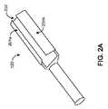
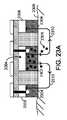
図2A及び図2Bは、図1の単一テール104の遠位端104aと係合された前後のコネクタ筐体120を示す。図2Aでは、コネクタ筐体120は、導電性接続部202と、フラップ204a及び204bとを含む。コネクタ筐体120を単一テール104の遠位端104aと係合させるため、遠位端104aを導電性接続部202とフラップ204a及び204bとの間に挿入して、単一テール104の遠位端104aが、導電性接続部202との電気的接触点となるようにする。そして、フラップ204a及び204bを、遠位端104aの上に折り畳んで、フラップ204a及び204bと導電性接続部2020との間において遠位端104aを機械的に固定する。一部実施形態では、フラップ204a及び204bも導電体製となり、一部実施形態では、コネクタ筐体120全体が導電性となる。フラップ204a及び204bを単一テール104の遠位端104a上に折り畳んだ後に、コネクタ筐体120に一つ以上の波形ができるようにそのコネクタ筐体を縮れさせて、単一テール104の遠位端104aを受容する波状レセプタクル122を形成する。これらの波形は追加的な引張強度を提供して、長手方向の力によって単一テール104からコネクタ筐体120が離れることを防止し、また、単一テール104と導電性接続部202との間の電気接続を改善する。波状レセプタクルは、一つ、二つ、三つ、又はそれ以上の波形を含み得る。 2A and 2B show the front and
図3は、一体電極300の分解図である。電極300は、導電性層312の頂部に沿って配置された非導電性頂部層310と、導電性層312の下に配置されたゲル層314とを含む。また、電極300は、導電性層312の下に部分的に配置され且つゲル層314の下に部分的に配置された延長部318を備えた非導電性底部層316も含む。非導電性頂部層310、導電性層312、ゲル層314、及び非導電性底部層316の材料及び配置は、図1の一体電極100の対応する構成要素に対して上述したものと同様である。導電性層312は、単一テール306も含み、その単一テール306はその遠位端306a及び張り出し部302を含む。導電性層312の張り出し部302、単一テール306及び本体307は、連続的な導体から形成される。また、非導電性底部層316も張り出し部320を含む。非導電性底部層316の張り出し部320は、単一テール306の張り出し部302と略同一の寸法を有し得る。一部実施形態では、導電性層312及び非導電性底部層326は同一の寸法に打ち抜かれる。 FIG. 3 is an exploded view of the
図3は、単一テール306の遠位端306aの張り出し部302上に配置された第二の導電性層308も示す。一部実施形態では、第二の導電性層308は、導電性層312とは異なる導電体から形成される。例えば、導電性層312がアルミニウムから形成され得て、第二の導電性層308が、カーボンストリップ、炭素を含浸させた導電性ポリ塩化ビニル又はポリウレタン等の導電性プラスチックとなり得る。第二の導電性層308は、単一テール306の張り出し部302に追加的な剛性を与え得る。一部実施形態では、第二の導電性層308によって与えられる追加的な剛性は、自動製造設備(例えば変換設備)によって電極300用のコネクタ内に張り出し部302を形成することを可能にして、結果的にコネクタの機械的強度を増加させ得る。更なる説明を、張り出し部302から形成されたコネクタの代表的な(非限定的)実施形態について以下に与える。図3は、非導電性材料から形成された底部支持層322も示し、これは、非導電性底部層316の張り出し部320に代えて又は加えて電極300内に含まれ得て、機械的支持を与える。 FIG. 3 also shows a second
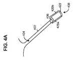
図4A〜図4Cは、図3に示される電極300から形成されたコネクタ400を示す。図4Aは、導電性層406の上に配置された非導電性頂部層404を示し、その遠位端に配置された張り出し部408を備えた電極テール402を形成している。張り出し部408は導電性層406の延長部であり、その上に配置された第二の導電性層422を有する。張り出し部408の側部420a及び420bを、例えばマンドリルや他の適切な製造プロセスを用いて、互いに向けて湾曲させる。図4Bは、側部420a及び420bを互いにくっつけて形成されるチューブ410を示す。側部420a及び420bを、シーリング、接着、又はホチキスによって互いに取り付け得て、又は単純に重ねることができる。図4Bは、熱収縮チューブ414のセグメントも示す。側部420a及び420bを近付けて、熱収縮チューブ414をチューブ410上に配置して、チューブ410を越えて単一テール406上にまで伸ばす。熱を加えると、好ましくは図4Cに示されるように、熱収縮チューブ414が、単一テール406及びチューブ410に対してコンフォーマルになる。熱収縮チューブ414がチューブに対してコンフォーマルになると、熱収縮チューブ414がチューブ410に対する機械的支持を提供し、単一テール406がチューブ410と電極の使用者との間の電気的絶縁を提供する。チューブ410は内部通路412を形成し、これは、電気刺激リード(図示せず)からの雄型ピンを受容するように形成される。張り出し部408上の第二の導電性層422は、接続及び接続解除による摩耗及び断裂に対してコネクタ400を強くするのに役立つ。導電性層406の単一テールの張り出し部408からコネクタ400を形成するプロセスは、自動化され得て、これは、電極の均一性を更に改善する。 4A-4C show a
図5はスナップ電極500の分解図である。電極500は、第一の開口516を備えた非導電性頂部層502と、第二の開口418を備えた導電性層504と、ゲル層506とを含む。非導電性頂部層502、導電性層504、及びゲル層506の材料及び配置は、図1及び図3の一体電極100及び300の対応する構成要素について上述したものと同様である。スナップ電極500は、第一の導電性筐体508と、導電性ポスト511を備えた第二の筐体510とを含み。その導電性ポスト511は第二の筐体510に固定されて、第一の導電性筐体508のレセプタクル(図示せず)内部にはまって、二つの筐体508及び510を接続する。第二の筐体510は、導電性層504の下に配置された第二の導電性筐体512を含む。第二の筐体510は、第二の導電性筐体512及び導電性層504の下であってゲル層506の上に配置された非導電性素子514も含む。第二の開口518は、第二の筐体510の一部を受容するようなサイズにされる。スナップ電極500を組み立てると、第二の筐体510が第一の導電性筐体508と係合して、層502及び504の開口516及び518を貫通するポスト511で、導電性層504及び非導電性頂部層502を挟み込む。 FIG. 5 is an exploded view of the
非導電性素子514は、誘電体ポリマー等の絶縁体から形成されて、第二の導電性筐体512のフットプリント以上の周囲寸法を有する。使用時には、電気刺激デバイスからの電流が、電気リード(図示せず)から第一の導電性筐体508、導電性層504及び第二の導電性筐体512へと流れる。そして、電流はゲル層506を介して患者組織に分布する。非導電性素子514は、電流が非導電性素子514の周りでゲル層506を通って流れるようにして、過度の電流が、第二の導電性筐体512の真下のゲル層506の一部を介して患者組織に向かう最小抵抗経路をとることを防止することによって、第一の導電性筐体508及び第二の導電性筐体512aの真下における熱及び電流の蓄積(ホットスポット)を防止する。従来のスナップ電極は、導電性層とゲル層との間に非導電性素子を含まず、直接的な電気の流れに起因してスナップコネクタの下にホットスポットを形成する傾向があり、これは患者組織を焼く可能性がある。電極500は、第二の導電性筐体512から患者組織までの経路内に非導電性障壁を配置することによって、このようなホットスポットの可能性を低下させて、ゲル層506に対するより均一な電流分布をもたらす。 The
図6は、第一の開口622を備えた非導電性頂部層620と、第二の開口618を備えた導電性層604と、ゲル層606と有するスナップ電極650の分解図である。非導電性頂部層620、導電性層604及びゲル層606の材料及び配置は、図1、図3及び図5に示される電極に対して上述したものと同様である。スナップ電極640は第一の導電性筐体608及び第二の筐体624を更に含む。第二の開口618は、第二の筐体624のポスト部613を受容するようなサイズにされる。スナップ電極650を組み立てると、第二の筐体624のポスト部613が第一の導電性筐体608と係合して、図5の電極500を参照して上述したように、導電性層604及び非導電性頂部層620に渡される。第一の導電性筐体608は、非導電性頂部層620の開口622を介して導電性層604と電気的に接触する。 FIG. 6 is an exploded view of a
第二の筐体624は、誘電体ポリマー等の電気絶縁体から形成される。図5のスナップ電極500と同様に、スナップ電極650も、第一の導電性筐体608の真下におけるホットスポットの形成を防止する。使用時には、非導電性の第二の筐体624が、第一の導電性筐体608からゲル層606を介して患者組織に向かう直接的な電気の流れに対する障壁として機能する。結果として、ゲル層606に対するより均一な電流分布が得られ、危険なホットスポットの可能性が減る。 The
図7及び図8は磁気コネクタ電極を示す。図7は、磁気コネクタ電極700の分解図である。電極700は、ソケット712と、開口708を備えた非導電性頂部層706と、導電性磁性層704と、導電性層702と、ゲル層722とを含む。非導電性頂部層706、導電性層702、及びゲル層722の材料及び配置は、図1、図3、図5及び図6に示される電極に対して上述したものと同様である。ソケット712は、プラスチックなどのリジッドな非導電性材料から形成されて、非導電性頂部層706の上に結合されるか、接着されるか、又は他の方法で固定される。導電性磁性層704は、非導電性頂部層706の開口708の下に配置される。導電性磁性層704は、ステンレス鋼等のフェライト材料から形成され得るが、他の導電性磁性体ともなり得る。導電性層702は、アルミニウム等の導体から形成され得る。導電性磁性層704は、非導電性頂部層706と導電性層702との間に配置される。非導電性頂部層706の底面上の接着剤で、非導電性頂部層706と導電性層702との間に導電性磁性層704を挟み込むことによって、磁気コネクタ電極700を組み立てた際に導電性磁性層704を適所に保持する。 7 and 8 show magnetic connector electrodes. FIG. 7 is an exploded view of the
図8は、磁気コネクタ電極850の分解図である。電極850は、開口810を備えた非導電性頂部層820と、ソケット814と、導電性磁性層804と、導電性層802と、ゲル層822とを含む。図7の磁気コネクタ電極700とは異なり、図8の磁気コネクタ電極は、非導電性頂部層820の下に配置されたソケット814を有する。図8に示されるソケット814の具体的な実施形態は、頂部816及び底部818を有し、頂部816の直径が底部818の直径よりも小さくて、ソケット814の側部が、頂部816と底部818との間に張り出している。電極850が組み立てられると、ソケット814の頂部816が、非導電性頂部層820の開口を貫通する一方で、ソケット814の底部818は非導電性頂部層820の下に留まる。導電性磁性層804はソケット814の下に配置される。例えば、非導電性頂部層820と導電性層802との間の接着結合を用いて、ソケット814及び導電性磁性層804の両方が非導電性頂部層820と導電性層802との間に挟み込まれる。 FIG. 8 is an exploded view of the
図7及び図8の磁気コネクタ電極は、一以上の有利な特徴を与える。第一に、磁気接続機構の使用によって、患者又は医師が電極を接続又は接続解除するために機械的抵抗力を克服しなければならないスナップ接続機構と比較して、より滑らかな垂直方向における接続及び接続解除が得られる。関節炎の又は障害のある使用者が電極を接続及び接続解除することを容易にして、損傷した又は敏感な組織に不快な力を印加することを回避する。第二に、導電性磁性層(図7の層704、図8の層804)は、磁気リードコネクタ(図9の磁気リードコネクタ904等)に含まれる磁石に引き寄せられるので、使用者が、図7及び図8の磁気コネクタ電極を背中等の見ることが難しい体の箇所に対して適所に適用及び接続することが簡単である。第三に、ソケット712及び814は、磁気リードコネクタ(図9に示される磁気リードコネクタ902等)が導電性磁性層(図7の層704、図8の層804)と整列するように患者や医師が磁気リードコネクタを配置するのに役立ち、電極に対して磁気リードコネクタを保持するのに十分な磁気結合が得られる。一部実施形態では、ソケット(ソケット712や814等)の形状は、相補的形状の磁気リードコネクタのみがソケット内に収容されるように選択され得る(ソケットとコネクタの“鍵”と称する)。ソケット及びコネクタの鍵は、製造業者が一緒に機能するように設計された磁気リードコネクタと電極との組み合わせを製造して、治療的に有用ではなくなり得る他の磁気リードコネクタと電極との組み合わせの使用を防止することを可能にする。第四に、ソケット712及び814は、横方向の力(図9に示されるリードワイヤ908に対する急な強い引っ張り等)によって磁気リードコネクタから電極から接続解除されることを防止する機械的障壁を提供する。病院では、横方向の引っ張りが接続解除の事象におけるかなりの割合を占めている。導電性磁性層(図7の層704、図8の層804)と磁気リードコネクタに含まれる磁石との間の磁力は、垂直方向よりも横方向において弱いので、ソケット712及び814がこのような引っ張りに対する追加的に安全性を提供する。 The magnetic connector electrodes of FIGS. 7 and 8 provide one or more advantageous features. First, the use of a magnetic connection mechanism allows for a smoother vertical connection and a smoother connection compared to a snap connection mechanism where the patient or physician must overcome mechanical resistance to connect or disconnect electrodes. Disconnection is obtained. It makes it easier for arthritic or disabled users to connect and disconnect electrodes and avoids applying unpleasant forces to damaged or sensitive tissue. Second, the conductive magnetic layer (the
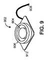
図9は、電気刺激デバイス(図示せず)からのリードワイヤ908を図7又は図8の磁気コネクタ電極に係合させるのに使用可能な磁気リードコネクタ902を示す。磁気リードコネクタ902はコネクタベース部912を含み、その上に磁石904が固定される。磁石904はネオジム等の導体製であり、リードワイヤ908に電気的に接続される。一部実施形態では、磁石904が、リードワイヤ908又は中間導電性素子(図示せず)にはんだ付けされる。一部実施形態では、好ましくは、磁石904は、低温のままに保たれて、磁石904の結晶構造の変化や磁性への影響を防止する。一部実施形態では、磁石904は、金属の鉤爪システムを用いてコネクタベース部912に対して保持されて、その金属の鉤爪システムは、磁石904と摩擦でフィットするように形成された雌型受容器を含む。一部実施形態では、接着剤(導電性接着剤等)を用いて、磁石904をコネクタベース部912に取り付けることができる。図9の磁気リードコネクタ902は、外壁906も含み、その外壁906は、非導電性材料から形成され得て、また、電極のソケットを取り囲むように構成され得る(図7のソケット712や、図8のソケット814の頂部816等であり、それぞれの図面に示される電極に磁気リードコネクタ902が係合した場合)。外壁906は、追加的な引っ張り強度を与え得て、リードワイヤ908に対する横方向の急な強い引っ張り等の横方向に印加される力によって、磁気リードコネクタ902が磁気コネクタ電極との接続状態からずれることを防止する。磁気リードコネクタ902の一部実施形態では、外壁が含まれない。磁気リードコネクタ902が図7の電極700又は図8の電極850に取り付けられる場合、磁石904はソケット712又は814内に収容されて、磁石904と導電性磁性層(図7の層704、図8の層804)との間の電気接続が得られる。使用時には、電気刺激電流が、電気刺激電流発生器(図示せず)から、リードワイヤ908、磁石904、導電性磁性層を通って、導電性層(図7の層702、図8の層802)に向かい、そして、ゲル層(図7の層722、図8の層822)を通って、患者組織に向かう。 FIG. 9 shows a
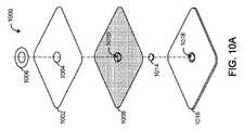
図10A及び図10Bは、本願で説明される一体電極の構成法に従って形成可能な反転スナップ電極1000を示す。図10Aは反転スナップ電極1000の分解図である。反転スナップ電極1000は、開口1004を備えた非導電性頂部層1002を含み、その開口1004は、非導電性頂部層1002の上又は内部に配置された強化リング1006によって取り囲まれている。強化リング1006は、非導電性材料(例えば、非導電性層や絶縁層としての使用に適していると本願で説明されるような材料)から成り、使用時にスナップコネクタを反転スナップ電極1000に対して接続及び接続解除する際における反転スナップ電極1000に対する機械的な強化を与え得る。反転スナップ電極は、くぼみ1010を備えた導電性層1008と、くぼみ1018を備えたゲル層とも含む。非導電性頂部層1002、導電性層1008、ゲル層1016の材料は、図1及び図3の一体電極100及び300の対応する構成要素に対して上述したものと同様である。非導電性素子1014は、導電性層1008のくぼみ1010とゲル層1016のくぼみ1018との間に配置される。図10Bは、図10Aの反転スナップ電極の断面図であり、非導電性頂部層1002と、導電性層10089と、くぼみ1010と、ゲル層1016と、くぼみ1018と、非導電性素子1014とが含まれている。 10A and 10B show an
導電性層1008のくぼみ1010は、ロール製造プロセス中における熱成形や真空成形等の多様な方法で機械的に形成可能である。くぼみ1010は、導電性層1008内部に雄型コネクタ(例えば、以下で詳述される図11のコネクタ1100の雄型部1010)を受容するような雌型レセプタクルとして形成される。一部実施形態では、くぼみ1010は、標準的な雄型スナップコネクタをぴったりと受容するような寸法とされる。一部実施形態では、くぼみ1010は、カスタマイズされたサイズ又はカスタマイズされた形状の雄型コネクタをぴったりと受容するような寸法とされる。カスタマイズされた雄型コネクタは任意の深さや、幅、長さ、形状を有し得て、“鍵型”コネクタとして機能し得て、くぼみ1010によって形成されたレセプタクルに対して相補的な形状を有するコネクタのみが、反転スナップ電極1000としっかり係合することができる。反転スナップ電極1000(又は、本願で説明されるいずれかの電極及び電極システム)と共に鍵型コネクタを使用すると、(一群の鍵型電極のうちの)誤った電極が所定の電気治療デバイスと共に使用される可能性や、電気治療デバイス製造業者の許可なく製造された低品質の電極が鍵型コネクタと上手く係合してしまう可能性を低下させることによって、治療結果を改善し得る。 The
特定の組み立てモードにおいて、非導電性素子1014が、導電性層1008とゲル層1016との間において、導電性層1008のくぼみ1010の底面の下に配置される。ゲル層1016のくぼみ1018は、くぼみ1010及び非導電性素子1014の形状と相補的であるが、好ましくは、ゲル層1016の底面を越えては延伸せず、平坦なゲル表面が患者組織に適用されるようにする。好ましい実施形態では、くぼみ1010を形成して非導電性素子1014を配置した後に、ゲル層1016を導電性層1008上に流し込んで、その後、ゲル層1016が適所で架橋する(これを“適所流し込み(pour−in−place)”プロセスと称する)。ゲル層1016及びそのくぼみ1016は、モールドでも形成され得るし、複数の個別のシートからも形成され得る。図5の非導電性素子514について上述したように、非導電性素子1014は、電流が非導電性素子1014周りでゲル層1016を通って流れるようにして、過度の電流が、くぼみ1010の真下におけるゲル層1016の部分を通って患者組織に向かう最小抵抗経路をとることを防止することによって、くぼみ1010の下に“ホットスポット”が形成されることを防止する。 In a particular assembly mode, a
反転スナップ電極1000は、標準的なスナップ電極に対して複数の利点を有し得る。第一に、(スナップ電極に基づいたシステムにおいて典型的なコネクタ内部ではなくて)電極自体の内部に雌型レセプタクルを含むことによって、雄型コネクタの深さが電極の厚さ内部に留められるので、反転スナップ電極1000は、既存のスナップ電極システムよりも薄い形状を提供する。この薄い形状は、ギプスや支持具内部といった既存のスナップ電極が適していない治療設定において反転スナップ電極1000を使用することを可能にする。また、反転スナップ電極1000の薄い形状は、患者が動いた際に電極又はコネクタが患者の衣服や他の物体にひっかかる可能性を減らして、既存の電極よりも活動的な患者(例えば、運動療法中の患者)の電気刺激やモニタリングにより適したものとなり得る。また、小型のリードピンを電極のリードワイヤの端部のソケット内に供給しなければならない従来の“薄い形状”の電極よりも、反転スナップ電極1000は使い易い。年配の患者にとっては一般的にリードピンの構成よりもスナップ電極の方が使い易いので、これは、特に年配の患者にとって有用である。また、導電性層1008を形成するのにロール材料(アルミニウムラミネート等)を使用することや、ゲル層1016を追加するのに適所注ぎ込みプロセスを用いることによって、手作業で組み立てられる電極や、製造中の多数の段階において材料を手動で移送して投入しなければならない機械によって組み立てられる電極と比較して、効率、信頼性、及び均一性が改善されて、製造上の利点を得ることができる。
図11は、コネクタ1100の斜視図であり、このコネクタ1100は、図10の反転スナップ電極1000等の反転スナップ電極とリードワイヤ1106を係合させるように構成されている。コネクタ1100は、コネクタベース部1104を含み、その上に雄型部1102が配置される。雄型部1102は、導体製であり、リードワイヤ1106に電気的に接続される。一部実施形態では、雄型部1102は、上述の反転スナップ電極1000の導電性層1008のくぼみ1010を形成するためのものと同じ又は同様の製造法(例えば、真空成形や熱成形)を用いて形成され、また、導電性層1008と同じ又は同様の材料から形成され得る。図示されるように、雄型部1102は、コネクタベース部1104から開口1110を通って非導電性頂部層1108内に延伸している。コネクタベース部1104と向き合う非導電性頂部層1109の表面は接着性であり得て、非導電性頂部層1108とコネクタベース部との間において雄型部1102を機械的に捕獲し得る。一部実施形態では、反転スナップ電極1000用のコネクタに非導電性頂部層1108が含まれず、雄型部1102が、接着剤、タブ、又は他の固定手段を用いて、コネクタベース部1104に固定される。リードコネクタ110を図10の反転スナップ電極1000に取り付けると、雄型部1102が、くぼみ1010によって形成されたレセプタクル内部に収容されて、リードワイヤ1106と導電性層1108との間の電気接続が得られる。使用時には、電気刺激電流が、電気刺激電流発生器(図示せず)から、リードワイヤ1106を通って導電性層1108に流れ、そして、患者組織へと流れる。図10を参照して上述したように、コネクタ1100を反転スナップ電極1000と係合させると、これら二つが、既存のスナップ電極-コネクタ組み立て体よりも薄い形状を有し得て、性能が改善され、多様な治療及び診断環境における使用範囲が広がり得る。 FIG. 11 is a perspective view of the
電極設計の追加的なバリエーションも考えられる。例えば、図12は、上述の単一の本体及びテール構造と同様の複数の電極構造を含む電極システム1200の分解図である。電極システム1200は、非導電性頂部層1202と、第一の電極1204と、絶縁層1206と、第二の電極1208と、ゲル層1210とを含む。第一の電極1204及び第二の電極1208は、図1及び図3に関して上述したような単一の導電性材料から構成される。第一の電極1204は、単一テール1222及び本体を含む。絶縁層1206は、第一の電極1204の本体の1224の外径に略適合するようなサイズのホール1214を含む。第二の電極1208は、単一テール1220及び本体1221を含む。第二の電極1208の本体1221は、絶縁層1206の外径に略適合するようなサイズのホール1212を含む。ゲル層1210は、第一のゲルセグメント1210a及び第二のゲルセグメント1210bを含む。第一のゲルセグメント1210aは、第二の電極1208の本体1221の寸法に略適合するようなサイズにされ、第二のゲルセグメント1210bは、第一の電極1204の本体1224の寸法に略適合するようなサイズにされる。非導電性頂部層1202は、第二の電極1208の本体1221の外径に略適合する外径を有し得る。非導電性頂部層1202の底面には接着剤がコーティングされ得て、その接着剤に、第一の電極1204、絶縁層1206及び第二の電極1208が付着し得る。これらの構成要素が非導電性頂部層1202に付着すると、絶縁層1206の厚さが、第二の電極1208の底面の下まで延伸し得て、第一のゲルセグメント1210a及び第二のゲルセグメント1210bがその組み立て体の底部に付着した際に、絶縁層1206の底部が、ゲル層1210の底部と略同一の平面内に存在して、実質的に均一な表面が患者組織に付着するようになる。 Additional variations in electrode design are possible. For example, FIG. 12 is an exploded view of an
図13は、図12の電極システム1200の説明に従って構築された電極システム1300の分解図である。電極システム1300は、非導電性頂部層1302と、第一の電極1304と、絶縁層1306と、第二の電極1308と、ゲル層1310とを含む。第一の電極1304及び第二の電極1308は、図1、図3及び図12を参照して上述したように、単一の導電性材料から構成される。第一の電極1304は、単一テール1322と、本体1324と、ホール1316とを含む。絶縁層1306は、第一の電極1304の本体1324の外径に略適合するようなサイズのホール1314を含む。第二の電極1308は、単一テール1320と、ホール1312を備えた本体1321とを含み、そのホール1312は、絶縁層1306の外径に略適合するようなサイズにされる。ゲル層1310は、第一のゲルセグメント1310a及び第二のゲルセグメント1310bを含む。ゲルセグメント1310aの寸法は、第二の電極1308の本体1321の寸法に略適合するようなサイズにされ、ゲルセグメント1310bの寸法は、第一の電極1304の本体1324の寸法に略適合するようなサイズにされる。 13 is an exploded view of
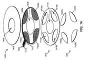
図14は、電極システム1400の分解図である。電極システム1400は、ホール1406を備えた非導電性頂部層1404を含む。更に、電極システム1400は、基板1412上に取り付け又は印刷された複数の導電性領域1402a、1402b、1402c及び1402dを含む。基板1412は、各導電性領域1402に対する導電性トレース1422を備えたテール部1414を含む。更に、基板1412はホール1408を含む。また、電極システム1400は、複数の開口1418a、1418b、1418c及び1418dを有する絶縁層1416も含む。各開口1418は、各導電性領域1402と整列するように配置される。更に、絶縁層1416は、ホール1408及びホール1406と同心円状に整列したホール1410を含む。また、電極システム1400は、複数の下セグメント1420a、1420b、1420c及び1420dを有するゲル層1422も含む。電極システム1400を組み立てると、各ゲルセグメント1420は、絶縁層1416の各開口1418内に配置される。電極システム1400の使用時には、ゲルセグメント1420が、導電性領域1402と患者組織との間に介在する。 FIG. 14 is an exploded view of the
電極システム1400は、特に、2チャンネル干渉性電気刺激及びTENS治療に向いている。電極システム1400の中心のホールは、医師用の作業領域を与え、縫合や、ドラッグデリバリー用のニードルスティック、検査等の他の医療行為の準備のための又はそれらの行為中に患者組織を麻痺させることができる。また、ホールは、患者組織に対して電極を適所に配置することも容易にする。つまり、患者又は医師が、各導電性領域を別々に配置することなく、患者の疼痛部位に対してホールを“中心に置く”ことができる。更に、電極システム1400の使い易さは、患者に対する電気治療の治療効果を実証する有利な方法を提供し、その患者はその使用からの利点を得ることができる。つまり、電極システム1400及び電気刺激を患者組織に素早く適用することができ、数秒の間に明確な効果が得られる。
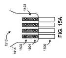
図15A及び図15Bはそれぞれ、接続素子を分離するために電極テール上の導電性トレースを電気的に接続するのに使用可能な接続システムの正面図及び背面図である。図15Aでは、テール1414は、四つの導電部1422を備えるものとして示されている。各導電部は、一組の第一の歯部1502及び一組の第二の歯部1504によって穴開けされ、第一及び第二の歯部は、複数のコネクタ1506に取り付けられる。コネクタ1506は第一の歯部1502及び第二の歯部1506を含み、導体から形成され、電極システム(図14の電極システム1400等)を電気刺激デバイス(図示せず)に電気接続するためにワイヤや他の導電性リードに取り付け可能である。図15Bは、導電部1422に取り付けられたコネクタ1506を備えたテール1414の背面図である。 FIGS. 15A and 15B are front and rear views, respectively, of a connection system that can be used to electrically connect conductive traces on the electrode tail to separate the connection elements. In FIG. 15A, the
図16は、患者の指1602に配置されたカスタマイズ切断された電極1600の斜視図である。一部実施形態では、医師又は患者が、患者組織の特定の輪郭にフィットするように本願で説明される一体電極(導電体の連続片から一体形成された電極本体及び電極テールを含む)を切断することができる。例えば、医師は、患者の指1602の治療領域にフィットするように、一般的なハサミを用いて大きな電極(例えば、図1及び図3の電極)から図16の電極1600を切り出すことができる。従来の電極は、導電性ポリマーに対する多様な接触点を形成するために扇状に広げられた多重ストランドテールを含むので、扇状に広げられたストランドを損傷させずに、このように切断することができないものである。本願で説明される電極は、患者固有の輪郭及び治療目標に対して電極の形状及びサイズを医師がカスタマイズすることを可能にして、電気刺激の伝達を改善する。 FIG. 16 is a perspective view of a customized
図17及び図18はそれぞれ、二つのリボン状電極1700及び1800の平面図である。各電極は、一体形成されたテールを備える導電性層を含む。一部実施形態では、電極1700及び1800の本体の寸法は略3/4インチ×5インチであるが、他の寸法も使用可能である。図17の電極1700のテール1702は、電極1700の主軸に対して長手方向に向けられているが、図18の電極1800のテール1802は、電極1800の主軸に対して垂直に向けられている。こうしたリボン状電極は、手首や膝等の患者の身体の一部の周りに巻かれ得る。本願で説明される一体構築法は、扇状に広げられた金属接続に起因するホットスポットや異種金属の腐食の危険性がなく、リボン状電極1700及び1800等の多様な形状の電極を製造することを可能にする。 17 and 18 are plan views of two ribbon-
図19Aは、電極本体1900(本願で説明されるいずれかの電極と共に使用可能である)の一部の断面図である。非導電性頂部層1904が導電性層1906の上に配置されて、導電性層1906を覆う。追加的な導電性層及び非導電性層も電極本体1900(又は他の電極本体)に含まれ得るが、簡単のため、図19Aには示されていない。ゲル層1908が、導電性層1906の下に配置され、ゲル層1906に隣接したゲルコーティング1910が本体1900の側部まわりに延在して、導電性層1906の周囲側面1902を覆う。周囲側面1902上のゲルコーティング1910の存在は、電流がゲルコーティング1910又はゲル層1908を迂回して、患者又は医師の組織に直接入り込み、痛みを伴うショックや不均一な電流分布を生じさせるのを防止するのに役立つ。図19Aに示されるゲルコーティング1910の構成を、例えば、材料層から電極を打ち抜くことによって得ることができる。 FIG. 19A is a cross-sectional view of a portion of electrode body 1900 (which can be used with any of the electrodes described herein). A
図19Bは、電極テール1920(本願で説明されるいずれかの電極と共に使用可能であり、例えば、電極本体の単一延長部として本願で説明される)の断面図である。電極テール1920は、非導電性頂部層1922と、導電性層1924と、非導電性底部層1926とを含む。追加的な導電性層及び非導電性層も電極テール1920に含まれ得るが、簡単のため、図19Bには示されていない。電極テール1920は、左側面1928a及び右側面1928bも含む。絶縁コーティング1930が側面1928に沿って配置されると、電極テール1920の側部に沿った患者若しくは医師と導電性層1924との間における、又は導電性層1924と他の電気的に晒された表面(他の電極のテール等)との間における意図していない電気接触を防止するのに役立つ。図示されるように、絶縁コーティング1930bは、左側面1928aを覆う左コーティング領域1930aと、右側面1928bを覆う右コーティング領域1930bとを有する。一部実施形態では、絶縁コーティング1930は、液状で適用されるシリコーンである。 FIG. 19B is a cross-sectional view of an electrode tail 1920 (which can be used with any of the electrodes described herein, eg, described herein as a single extension of the electrode body).
自動製造プロセスを用いて、本願で説明される電極を形成することができる。一部実施形態では、電極は、特に接着剤の分配、積層化、及び切断によってロールストックから電極を製造する回転変換機を用いて形成される。二つ目の自動製造プロセスを用いて、コネクタ(図4A〜図4Cに示される単一導電性テール406の張り出し部408から形成されたコネクタ400等)を形成したり、コネクタ(図2A〜図2Bに示される波状レセプタクル122を備えたコネクタ筐体120や、図15A〜図15Bに示されるコネクタ1506等)を取り付けたりすることができる。 An automated manufacturing process can be used to form the electrodes described herein. In some embodiments, the electrodes are formed using a rotary transducer that produces the electrodes from roll stock, particularly by adhesive dispensing, lamination, and cutting. A second automated manufacturing process can be used to form a connector (such as the
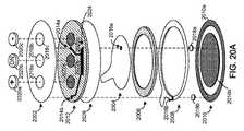
図20Aは、電子機器層2012を備えた刺激システム2000の分解図である。図12の電極システム1200と同様に、刺激システム2000は、複数の電極構造を含む。特に、刺激システム2000は、非導電性頂部層2002と、第一の電極2004と、絶縁層2006と、第二の電極2008と、ゲル層2010とを含み、そのゲル層2010は、第一のゲルセグメント2010a及び第二のゲルセグメント2010bを有する。第一の電極2004及び第二の電極2008は、図12の対応する構造を参照して上述したように構築され、非導電性頂部層2002、絶縁層2006及びゲル層2010についても同様である。図12の電極システム1200とは異なり、刺激システム2000は、非導電性頂部層2002及び第一の電極2004の下に配置された電子機器層2012を含む。非導電性層2026が電子機器層2012と第一の電極2004との間に配置される。一部実施形態では、非導電性層2026は、電子機器層2012の底面又は第一の電極2004の頂面の上の非導電性材料(非導電性プラスチック等)のコーティング状となる。 FIG. 20A is an exploded view of a stimulation system 2000 that includes an
電子機器層2012は、一以上の電気刺激処置を実施するための回路を含む。一部実施形態では、電子機器層2012は、所定の又はプログラム可能な電気刺激プロトロコルを実施するようにパッシブ電気部品及びアクティブ電気部品を備えて構成された印刷回路板を含む。これらの電気部品は、機械実行可能ロジックを備えて構成された一つ以上の制御マイクロプロセッサを含み得て、電子機器層2012に含まれる一つ以上の電源(印刷型又はコイル型の電池)からのエネルギーを、第一の電極2004及び第二の電極2008の一方又は両方を介して患者組織内に流すことのできる電気刺激電流に変換することを制御する。電子機器層2012は、回路部品を接続する一つ以上のサブ層(図示せず)の上に導体の印刷トレースを含み得る。電子機器層2012に含まれる回路部品の間に、パルス発生器2024が存在する。パルス発生器2024は、第一の電極2004及び第二の電極2008を介してそれぞれ患者組織に伝えられる二つの異なるチャネルの電気信号を発生させる。以下、図21〜図24を参照して、パルス発生器の多様な例示的実施形態について説明する。 The
刺激システム2000において、電子機器層2012は、接触点2014a(電子機器層2012内の)及び2016a(第一の電極2004内の)を介して第一の電極2004に電気的に接続される。これらの接触点2014a及び2016aは、穴開けによって電気的に接続されて、電子機器層2012内の接触点2014aが、第一の電極2004の接触点2016aと整列して且つ隣接して配置されて、電子機器層2012及び第一の電極2004が、接触点2014a及び2016aにおいて穴開けされて、電子機器層2012に含まれる導体と第一の電極2004との間に電気接続が形成される。一部実施形態では、ピンやロッド又は他の硬い部材を電子機器層2012の導電部を貫通するようにさして、導電部を変形させて、電子機器層2012から離れるように延伸する導体の突出部によって囲まれたホールを形成することによって、穴開け接続が形成される。一部実施形態では、突出部はギザギザで不規則であるが、他の実施形態では、導電性層の本体に予め切れ目が付けられていて、又は、突出部がより規則的な間隔及びサイズになるように作製される。電子機器層2012を非導電性層2026によって第一の電極2004から離隔すると、突出部が非導電性層2026を通って延伸して、第一の電極2004に対して折り曲げられて、電子機器層2012の導電部と第一の電極2004との間の電気接続が形成される。一部実施形態では、電子機器層2012、非導電性層2026及び第一の電極2004が積層されて、その全積層体に対して穴開け工程が行われる。 In the stimulation system 2000, the
電子機器層2012が、穴開け箇所以外の全ての点において非導電性層2026によって第一の電極2004から分離されるので、接触点2014a及び2016a間の穴は、パルス発生器2024の適切なチャネル(例えば、第一のチャネル)が発生させた電気信号を、電子機器層2012の残りの構成要素を短絡させることなく、第一の電極2004まで流すことができる。図20には、電子機器層2012と第一の電極2004との間に一つの接触点のみが示されているが、任意の数の接触点を用いることができる。また、刺激システム2000は、接触点2016aの下に配置された非導電性素子2018aも含み、上述のようにゲル層2010内部でのホットスポットの形成を防止し得る。 Since the
一組以上の同様の接触点を設けることができる。図20Aに示されるように、第二の組の接触点2014b及び2016bがそれぞれ電子機器層2012、第二の電極2008に含まれる。パルス発生器2024の第二のチャネルで発生した電気信号を第二の電極2008に送信する。接触点2014b及び2016bは、上述の穴開け法を用いて接続される。また、刺激デバイス2000は、接触点2016bの下に配置された非導電性素子2018bも含む。図20Bは、図20Aの刺激デバイスの断面図である。図20には二つの電極及び単一の電子機器層が示されているが、任意の数の電極及び任意の数の電子機器層を所望の配向で配置して用いることができる(本願で説明されるいずれかの電極等)。この接続構造を用いて、パルス発生器2024の異なる複数の出力チャネルを、かさばるワイヤを用いたり手作業ではんだ付けする必要なく、刺激システム2000内部の異なる複数の電極に向けることができる。一部実施形態では、穴開け接続は、電子機器層2012、第一の電極2004、第二の電極2008、非導電性層2026を提供する材料ロールに作用する回転変換設備によって形成される。本願で説明される電極及びシステムの製造における穴開けプロセスや他のステップは、以前では実現不可能であった構造の効率的な製造を可能にして、製造された製品の品質を改善し得る。例えば、自動電極製造プロセスは、手作業の組み立てプロセスよりも監視が簡単であり(例えば、カメラや他のセンサを用いて)、製造エラーをより簡単に検出することを可能にして、不適切な電極が市場に投入されることを防止する。 One or more sets of similar contact points can be provided. As shown in FIG. 20A, the second set of
電子機器層2012は、電気スイッチ2022a、2022b及び2022cも含む。これらの電気スイッチは、スイッチの表面上に働く力に対して電気的応答を提供する部品であり、ボタンの押下又は他のユーザー入力を検知するためのユーザーインターフェースの設計において一般的に用いられている。三つのボタン2020a、2020b及び2020cがそれぞれ電気スイッチ2022a、2022b及び2022cの上に配置されて、非導電性頂部層2002の開口2018a、2018b及び2018cと整列される。電気スイッチ2022a、2022b及び2022cは、電子機器層2012に含まれるマイクロプロセッサや他の回路と電気通信して、刺激システム2000によって与えられる電気刺激を開始又は調節する。図20Aに示されるように、“ON”と記された電源ボタン2020bを使用者又は医師が押して、電気スイッチ2022bを作動させて、電気刺激を開始(停止)させることができる。それぞれ“+”、“−”と記されたボタン2020a、2020cは、患者又は医師がこれらのボタンを用いて、強度調節スイッチ2022a及び2022cを作動させて、刺激デバイス2000によって与えられる電気刺激の強度を上げ下げする(又は、発生する刺激電流の振幅又は周波数を変更する)ためのものである。キー2020a、2020b及び2020cの代わりに又はこれらに加えて使用可能な追加的なユーザーインターフェースがMueller等の特許文献1に開示されていて、その全内容は参照として本願に組み込まれる。 The
刺激デバイス2000の電子機器層2012に含まれる回路は、一以上の電気刺激プロトコル(つまり、所定の電流又は電圧の波形)を発生させるように構成され得る。こうした電気刺激プロトコルは、電子機器層2012に含まれるメモリ(EEPROM等)や、論理ゲートや他の回路(例えばASIC)を用いて回路内にエンコーディングされ得る。一部実施形態では、刺激デバイス2000は、電源ボタン2020bを押した際に単一の電気刺激プロトコルを提供するように構成される(例えば、特定のTENS治療や特定のイオン導入治療)。単一の電気刺激プロトコルは、特定の症状(例えば、痛みや筋肉の張り)を処置することを対象としたものであり得て、刺激システム2000がパッケージングされて、患者組織に対して刺激システム2000を配置する方法の説明書と共に、医師及び患者に提供される。そして、刺激システム2000を作動させて、電源ボタン2020bを押下することによって電気治療が与えられる。一部実施形態では、刺激システム2000は、電源ボタン2020bを押しても反応しなくなる前に所定の回数のみ使用できる。刺激システム2000をオンにした回数は、電子機器層2012に含まれるEEPROMや他のメモリに記憶され得て、マイクロプロセッサが、最大使用回数を表す固定値に向けてカウントアップ又はカウントダウンを行うように構成され得る。一部実施形態では、電気刺激プロトコルは、所定の期間(例えば、30分間)にわたって電気刺激処置を提供し得る。その期間は、電子機器層2012に含まれるタイマー回路や、電子機器層2012の化学的な又は他のスイッチによって守られ得る。 Circuits included in the
一部実施形態では、刺激デバイス2000の電子機器層2012に含まれる回路は、イオン導入処置及びそれに続くTENS処置を提供するように構成される。このような実施形態では、ゲルセグメント2010a及び2010bが、ドラッグデリバリー容器に交換されて、その容器は、第一の電極2004及び第二の電極2008を介してDC(直流)電流が印加された際に容器から患者の皮膚内に届けられる帯電化合物を含んでいる。ドラッグデリバリー容器は、例えば、ドラッグデリバリーマトリクスを含み得て、その中に治療化合物が懸濁されている。 In some embodiments, circuitry included in the
図21は、イオン導入及びTENS治療を提供するように構成された刺激システム(図20の刺激システム2000等)の動作を示すフロー図である。ステップ2102では、刺激システム2000が、治療化合物を患者組織内に届ける電場を印加することによって、イオン導入処置を提供する。ステップ2104において、刺激システム2000が、イオン導入処置時間が経過したことを検知すると、刺激システム2000は、TENS処置の提供を開始する。上述のように、刺激システム2000は、電子機器層2012に含まれるタイマー回路を用いて、又は電子機器層2012の化学的又は他のスイッチによって、イオン導入処置時間が経過したことをステップ2104において決定し得る。 FIG. 21 is a flow diagram illustrating the operation of a stimulation system (such as the stimulation system 2000 of FIG. 20) configured to provide iontophoresis and TENS therapy. In step 2102, the stimulation system 2000 provides an iontophoretic treatment by applying an electric field that delivers the therapeutic compound into the patient tissue. In
イオン導入処置及びTENS処置の提供は、同じ組の電極(つまり、第一の電極2004及び第二の電極2008)を用いて行われ得るが、これらの電極には異なる波形が印加される。図22は、波形2200の第一の部分2200aの間イオン導入処置を提供して、波形2200の第二の部分2200bの間TENS処置を提供するために刺激デバイス2000が発生させる例示的な波形2200を示す。第一の部分2200aはDC部分であり、期間TIにわたる第一の電極2004と第二の電極2008との間の一方通行の電流を表す。波形2200の第一の部分2200aは、治療化合物を患者組織内に届ける電場を提供する。イオン導入処置が図23Aに示されていて、電流が、第一の電極2004(及びこれに対応する容器2302)と第二の電極2008(及びこれに対応する容器2304)との間で患者組織2308を通って一方向に印加されている。結果として、治療化合物2306が患者組織2308内に届けられる。The provision of iontophoretic treatment and TENS treatment can be performed using the same set of electrodes (ie,
刺激デバイス2000がイオン導入処置の時間が終了したと決定すると(図22の垂直線2202で表される)、刺激デバイス2000の電子機器層2012に含まれる回路が、AC(交流)波形を発生し始める。一部実施形態では、この回路は、Hブリッジトランジスタ構成を含む。図22に示される第二の部分2200bは矩形、二相性で対照的な波形であるが、他のAC波形も使用可能である。TENS処置が図23Bに示されていて、電流が、第一の電極2004(及びその対応する容器2302)と第二の電極2008(及びその対応する容器2304)との間において患者組織2308を介して二方向(矢印2310及び2312によって示される)に印加される。好ましい実施形態では、波形のTENS部分はDC成分を有さず、イオン導入処置時間に達した後においては、刺激システムが容器内に残存している治療化合物を送らないようにする。追加的に、残留化合物の存在は、刺激システムの電極と患者組織との間の境界における導電性を改善し得る。 When the stimulation device 2000 determines that the iontophoresis treatment time has ended (represented by the
好ましい実施形態では、イオン導入処置用のエネルギーを提供する(図21のステップ2102において)のと同じ電源(例えば、バッテリ)を用いて、TENS処置用のエネルギーを提供する(図21のステップ2106において)。既存の一部のイオン導入デバイスでは、イオン導入処置が完了した後に追加的なバッテリ電力が残り得るが、こうしたデバイスが使い捨てであれば、バッテリを捨てることで、そのエネルギーが失われる。対照的に、図21のプロセスに従って動作するように構成された刺激システムでは、バッテリに残っている電力を、TENS治療用の電流を発生させるのに用いることができて、その電流は、バッテリが枯渇するか又は所定の停止時間に達するまで続き得る。このように構成されたデバイスは、痛みを処置するためにイオン導入治療を受けている患者にとって特に有用であり、この場合、イオン導入処置に続いて痛みを和らげるTENS処置が患者の不快感を更に低下させ得る。追加的に、イオン導入処置と同じ物理的デバイスを用いてTENS処置を適用することによって、多数のデバイスを取り外したり適用したりすることに付随する皮膚の炎症を低減し、イオン導入処置及びTENS処置が患者の身体の別の場所に誤って配置される危険性を排除して、既存の技術を改善する。 In a preferred embodiment, the same power source (eg, a battery) that provides energy for iontophoretic treatment (in step 2102 in FIG. 21) is used to provide energy for TENS treatment (in step 2106 in FIG. 21). ). In some existing iontophoresis devices, additional battery power can remain after the iontophoresis procedure is completed, but if such devices are disposable, the energy is lost by throwing away the battery. In contrast, in a stimulation system configured to operate according to the process of FIG. 21, the power remaining in the battery can be used to generate a current for TENS therapy, which current is It can continue until it is depleted or a predetermined stop time is reached. Devices configured in this manner are particularly useful for patients undergoing iontophoretic therapy to treat pain, where TENS procedures that relieve pain following iontophoretic treatment further increase patient discomfort. Can be reduced. Additionally, applying the TENS procedure using the same physical device as the iontophoretic procedure reduces skin irritation associated with removing and applying multiple devices, and the iontophoretic and TENS procedures. Eliminates the risk of being misplaced elsewhere on the patient's body, improving existing technology.
図24は、図20の刺激システム2000の電子機器層2012に含まれ得る例示的な回路2010のブロック図である。回路2010は、電源2400と、パルス発生器2402と、電源スイッチ2404と、強度調節入力部2406と、出力部2408とを含む。電源2400は、回路2010の電力を提供し、例えば、一つ以上の印刷型又はコイン型の電池を含み得る。一部実施形態では、電源2400は、電力フィルタリング及び/又は電圧調節回路も含む。電源2400は、電源スイッチ2022b(図20)及びパルス発生器2402に電気的に結合される。電源スイッチ2022bは、電源ボタン2020b(図20)を介して使用者からの入力を受信して、回路2010に電力を供給するように電源2400と共に動作する。 FIG. 24 is a block diagram of an
パルス発生器2402は、第一の電極2004及び第二の電極2008(図20)を介して患者組織に伝えられる電気信号を発生させる。パルス発生器2402は、2チャネル出力部2408に電気的に結合されて、2チャネル出力部2408に電気信号を提供する。そして、2チャネル出力部2408の各チャネルは、第一の電極2004及び第二の電極2008(図20)の一方と接続されて、患者の治療箇所に電気信号を伝える。強度調節入力部2406(図20の強度調節スイッチ2022a及び2022cを含む)は、パルス発生器2402に電気的に結合されて、強度調節ボタン2020a及び2020c(図20)を介して使用者からの入力を受信する。強度調節入力部2406は、2チャネル出力部2408に送られる電気信号を強度を調節するようにパルス発生器2402と共に動作する。適切なパルス発生器のいくつかの例が、共にMorawetz等の特許文献2及び特許文献3に記載されていて、その全内容は参照として本願に組み込まれる。一部実施形態では、パルス発生器2402の発生させる電気信号は、単変調パルス(SMP,simple modulated pulse)信号である。他の構成及び電気信号も考えられる。 The
図25は、図24の回路2410を実現するのに使用可能な回路2500の電気回路図である。回路2500は、電源2500と、パルス発生器2502と、電源スイッチ2504と、振幅調節スイッチ2506と、出力部2508とを含む。電源2500は、バッテリ2512と、サーミスタ2514と、昇圧器2516と、他の電気部品とを含む。電源2500は、パルス発生器2502に電気的に結合されて、それに電力を供給する。また、電源2504は、コネクタブロック2520に電気的に結合されたものとして示されていて、そのコネクタブロック2520は、電源2500の電力を供給して、バッテリ2512を充電するのに用いられる。充電のエネルギーは、例えば家庭用電源や商用電源から得られ得て、電源出力や車両の電源を介して利用可能であり、12Vのコンセントを介してアクセス可能である。サーミスタ2514は、バッテリ2512とコネクタブロック2520との間に電気的に結合されて、バッテリ2512が充電中に過熱しないことを保証するためにバッテリの2512の温度を検出するのに用いられる。一部実施形態(使い捨ての応用のためのものを含む)では、図20の刺激システム2000の電子回路層に含まれる電源は充電可能ではなく、この場合、充電機能を提供する回路2500の構成要素は含まれない。 FIG. 25 is an electrical schematic of a
電源スイッチ2504は、回路2500をオン、オフにするのに用いられる。電源スイッチ2504は、例えば、上述のように、図20の電源ボタン2020bによって容易に制御可能である。一部実施形態では、電源スイッチ2504は、図示されるように、単極双投(SPDT, single-pole double-throw)スイッチである。また、電源2500は、昇圧器2516も含み、これは、バッテリ2512によって供給される電力の電圧レベルを所望の電圧レベルに上昇させるように動作する。パルス発生器2502は、電源2500から電力を受けて、電気信号を発生させる。電気信号は、パルス発生器2502によって提供されて出力部2508に送られる。パルス発生器2502は、振幅調節スイッチ2506を含む。振幅調節スイッチ2506は、例えば、図20の強度調節ボタン2020a及び2020cによって容易に制御可能である。この実施形態では、振幅調節スイッチ2506は電位差計である。電位差計が調節されると、パルス発生器2502が発生させる電気信号の強度がそれに応じて増大するか減少する。パルス発生器2502は、第一のタイマー2530及び第二のタイマー2532並びに図25に示されるような追加回路を含む。 The
また、パルス発生器2502は出力段2540も含む。簡単のため、図25に示される出力段2540には、1チャネル用の出力部(つまり、第一の電極2004及び第二の電極2008のうち一方に提供される出力部)しか示されていないが、第二の出力チャネルも同様に設けられる。出力段2540は、MOSFET2542及び変圧器2544を含む。出力段2540は、電気信号を出力部2508に送る前に電気信号の出力電圧を上昇させて、その出力部2508が患者組織に伝えるための電極に電気的に結合される。 The
図26は、図20の刺激システム2000の電子機器層2012に含まれ得る例示的な回路2600のブロック図である。この実施形態では、回路2600は、一次デジタル回路から形成される。回路2600は、電源2602と、バッテリ2604と、制御プロセッサ2606と、電源スイッチ2025b(図20)と、強度調節入力物2610と、データ通信デバイス2612と、データストレージデバイス2614と、出力段2616と、出力部2618とを含む。動作中において、電源2602はバッテリから2604から電力を受ける。電源2602は、電力を回路2600の他の構成要素に供給する前に、バッテリの電力を所望の電圧に変換する。電源2602はバッテリ充電器2630も含む。バッテリ充電器2630は、外部電源2620からの電力を受けて、バッテリ2604を充電する。図25を参照して上述したように、一部実施形態では、図20の刺激デバイス2000の電子機器層2012に含まれる電源は充電可能ではなく、この場合、充電機能を提供する回路2600の構成要素は含まれない。 26 is a block diagram of an
制御プロセッサ2606は、回路2600の動作を制御する。制御プロセッサ2606は、電源2602によって電力供給されて、出力段2616に提供される電気信号を発生させる。また、制御プロセッサ2606は、電源スイッチ2022b及び強度調節入力部2610にも電気的に結合される。制御プロセッサ2606は、電源スイッチ2022bの状態を監視する。制御プロセッサ2606が、電源スイッチの状態が変化したことを検出すると(例えば、使用者が図20の電源ボタン2020bを押すことに応答して)、制御プロセッサ2606は、それに応じて回路2600をオン又はオフにする。また、制御プロセッサ2606は、強度調節入力部2610(例えば、図20の強度調節スイッチ2022a及び2022c)の状態も監視する。制御プロセッサ2606が、強度調節入力部2610の状態が変化したことを検出すると(例えば、図20の強度調節ボタン2020a及び2020bを使用者が押したことに応答して)、それに応じて、制御プロセッサ2606は、出力段2616に提供される電気信号の強度を増大又は減少させる。 Control processor 2606 controls the operation of
制御プロセッサ2606は、コンピュータ可読ファームウェア2634を記憶しているメモリ2632を含む。ファームウェア2634は、制御プロセッサ2606によって実行されるソフトウェア命令及びアルゴリズムを含み、制御プロセッサ2606によって実行される論理演算を定める。ファームウェア2634のソフトウェア命令及びアルゴリズムを用いて、電気刺激デバイスを所望のモード(経皮電気神経刺激治療を提供するモードや、筋肉刺激治療を提供するモード等)で動作させることができる。一部実施形態では、回路2600は、データ通信デバイス2612を含む。データ通信デバイスは、有線又は無線の通信デバイスを含み、シリアルバス通信デバイス(例えば、ユニバーサルシリアルバス通信デバイス)、ローカルエリアネットワーク通信デバイス(例えば、イーサネット(登録商標)通信デバイス)、モデム、ワイヤレスエリアネットワークデバイス(例えば、802.11x通信デバイス)、ワイヤレスパーソナルエリアネットワーク通信デバイス(例えば、ブルートゥース(登録商標)通信デバイス)、他の通信デバイス等が挙げられる。データ通信デバイス2612を用いて、他のデバイスとデータを送受信することができる。例えば、データ通信デバイス2612を用いて、異なるバージョンのファームウェア2634を回路2600ダウンロードして、制御プロセッサ2606の動作を変更して、図20の刺激システム2000を所望のモード(イオン導入治療を提供するモード等)で動作させることができる。特定の実施形態では、ファームウェアアルゴリズムは、使用者によってダウンロード可能となる前に購入しなければならないものである。特定の実施形態では、使用者は、ファームウェアアルゴリズムをダウンロードする前に、ウェブサーバの患者インターフェース又は同様の他のインターフェースにアクセスしなければならない。また、回路2600は、メモリカードや他の既知のデータストレージデバイス等のデータストレージデバイス2614も含む。一部実施形態では、データストレージデバイス2614はメモリ2632の一部である。データ通信デバイス2612を用いて他のデバイスへのデータのアップロードを行うこともできる。例えば、制御プロセッサ2606は、データストレージデバイス2614内に電気刺激伝達の記録を記憶し得る。制御プロセッサ2606を用いて、データの記録をデータ通信デバイス2614に送信することによって、外部デバイスに治療の記録をアップロードすることができる。 Control processor 2606 includes memory 2632 that stores computer-readable firmware 2634. Firmware 2634 includes software instructions and algorithms executed by control processor 2606 and defines logical operations executed by control processor 2606. Software instructions and algorithms in firmware 2634 can be used to operate the electrical stimulation device in a desired mode (such as a mode providing transcutaneous electrical nerve stimulation therapy, a mode providing muscle stimulation therapy, etc.). In some embodiments, the
回路2600をオンにすると、制御プロセッサ2606は治療電気信号を発生させて、その信号を出力段2616に提供する。出力段2616は、電気信号を変換及びフィルタリングして、その電気信号を出力部2618に提供する。出力部2618は、図20の刺激システム2000の第一の電極2004及び第二の電極2008のうち一方に電気的に結合されて、電気信号を患者組織に伝える。図25を参照して上述したように、簡単のため、図26には、1チャネル用の出力部(つまり、第一の電極2004及び第二の電極2008のうち一方に提供される出力部)しか示されていないが、第二の出力チャネルも同様に設けられる。 When
図27は、図26の回路2600を実施するのに使用可能な回路2700の電気回路図である。回路2700は、回路2600の動作を制御する制御プロセッサ2706を含み、また、電源2702と、バッテリ2704と、電源スイッチ2708と、振幅調節スイッチ2710と、出力段2716と、出力部2718とも含む。また、上述のように、回路2700は、バッテリ2704を充電するのに使用可能な外部電源2720にも接続可能である。バッテリ2704(リチウムイオンバッテリであり得る)は、電源2702に電力を提供する。電源2702は、リチウムイオン充電管理制御装置(既製品として入手可能である)及び昇圧器2732並びに図示されている他の電気的構成要素を含む。また、電源2702は、上述のように5V DC電源等の外部電源2720に接続可能である。バッテリ2704が充電可能である一部実施形態では、バッテリ2704は、充電中のバッテリ2704の温度を監視するためのサーミスタを含む。 FIG. 27 is an electrical schematic of a
制御プロセッサ2706は、回路2700の動作を制御する。制御プロセッサ2706は、8ビットマイクロプロセッサを含み得て、又は、他のマイクロプロセッサ、中央処理装置(CPU,central processing unit)、マイクロコントローラ、プログラマブル論理デバイス、フィールドプログラマブルゲートアレイ、デジタル信号処理(DSP,digital signal processing)デバイス等の一以上の他の処理デバイスを含み得る。制御プロセッサ2706は、縮小命令セットコンピューティング(RISC,reduced instruction set computing)デバイスや、複数命令セットコンピューティング(CISC,complex instruction set computing)デバイス等の一般的なもの、又は、特定用途向け集積回路(ASIC,application specific integrated circuit)デバイス等の特別設計処理デバイスであり得る。
制御プロセッサ2706は、電源スイッチ2708及び振幅調節スイッチ2710に電気的に結合される。電源スイッチ2708は、制御プロセッサ2706に信号を提供し、それに応じて、制御プロセッサ2706が、オン状態とオフ状態とで回路2700を変更する。振幅調節スイッチ2710は、制御プロセッサ2706に電気信号を提供し、制御プロセッサ2706は、回路2700が発生させる電気信号の強度を調節するのに用いられる。制御プロセッサ2706が発生させる電気信号は、出力段2716に送られる。
出力段2716は、制御プロセッサ2706から受信した電気信号を適切なフォーマットに変換して、電気信号を出力部2718に提供する。簡単のため、図27に示される出力段2716には、1チャネル用の出力部(つまり、図20の通信システム2000の第一の電極2004及び第二の電極2008のうち一方に提供される出力部)のみが示されているが、第二の出力チャネルも同様に設けられる。図示されるように、出力段2716は、MOSFET2742及び変圧器2744を含む。他の実施形態では、変圧器2744が含まれず、フライバックコンバータや、適切な出力信号を発生させる他のコンバータが用いられる。 The output stage 2716 converts the electrical signal received from the
上述の説明は単に例示的なものであり、本願で与えられる詳細に限定されるものではないことを理解されたい。本開示には複数の実施形態が与えられているが、開示されるシステム、デバイス及び方法並びにそれらの構成要素が、本開示の範囲から逸脱せず、多数の他の具体的な形式で実現可能であることを理解されたい。 It should be understood that the above description is illustrative only and is not limited to the details provided herein. Although multiple embodiments are provided in this disclosure, the disclosed systems, devices and methods and components thereof can be implemented in numerous other specific forms without departing from the scope of this disclosure. Please understand that.
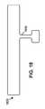
本開示を読んだ後においては、当業者には多様なバリエーション及び修正が想起されるものであり、開示される特徴を、本願で開示される一以上の他の特徴との任意の組み合わせ及びサブコンビネーションで実施し得る(多数の従属項の組み合わせ及びサブコンビネーション等)。上記で説明又は例示した多様な特徴(その構成要素を含む)は、他のシステムと組み合わせたり統合したりすることができるものであり、更には、特定の特徴を省略したり実施しなかったりし得る。 After reading this disclosure, various variations and modifications will occur to those skilled in the art, and the disclosed features may be combined with any combination and sub-configuration with one or more other features disclosed herein. Can be implemented in combinations (such as combinations of subordinate claims and subcombinations). The various features described or exemplified above (including their components) can be combined or integrated with other systems, and certain features may be omitted or not implemented. obtain.
変更例、置換例及び修正例は、本願で開示される情報の範囲を逸脱せずに当業者には実施可能なものである。本願でひかれる全ての参考文献は、その全体が参照として本願に組み込まれ、本願の一部を成すものである。 Modifications, substitutions, and modifications can be made by those skilled in the art without departing from the scope of information disclosed herein. All references cited in this application are incorporated herein by reference in their entirety and form part of this application.
100 一体電極
102 導電性層
104 単一テール
105 テール
106 非導電性頂部層
108 コネクタ
110 リードコネクタ
112 非導電性底部層
118 ゲル層
120 コネクタ筐体
122 波状レセプタクル
126 コネクタジャケットDESCRIPTION OF
Claims (64)
Translated fromJapanese前記テールの遠位端に配置されたコネクタと、
前記導電性層の頂部に沿って配置された非導電性頂部層と、を備えた電極。A conductive layer having a first region designed to apply therapeutic electrical stimulation to patient tissue and a second region with a tail configured as a single extension of said first region;
A connector disposed at a distal end of the tail;
An electrode comprising: a non-conductive top layer disposed along the top of the conductive layer.
前記非導電性頂部層の下に配置された導電性層と、
前記導電性層の下に配置されたゲル層と、
前記非導電性頂部層の上に配置された第一の導電性筐体及び前記導電性層の下に配置された第二の筐体を備えたスナップコネクタと、を備えた電極であって、
前記第二の筐体が、少なくとも部分的に非導電性であり、前記第一の導電性筐体と接続して前記導電性層及び前記非導電性頂部層に渡されるように構成されている、電極。A non-conductive top layer;
A conductive layer disposed under the non-conductive top layer;
A gel layer disposed under the conductive layer;
A snap connector comprising a first conductive housing disposed on the non-conductive top layer and a second housing disposed below the conductive layer;
The second housing is at least partially non-conductive and is configured to connect to the first conductive housing and pass to the conductive layer and the non-conductive top layer. ,electrode.
複数のコネクタと、
前記導電性領域の上に配置された非導電性頂部層と、を備えた電極システムであって、
各導電性領域が、単一テールを備えた導電性層を有する電極を含み、
各コネクタが、各単一テールの遠位端に配置されている、電極システム。A plurality of conductive regions;
Multiple connectors,
An electrode system comprising a non-conductive top layer disposed over the conductive region,
Each conductive region includes an electrode having a conductive layer with a single tail;
An electrode system, wherein each connector is located at the distal end of each single tail.
前記導電性層の頂部に沿って配置された導電性磁性層と、
前記導電性磁性層の頂部に沿って配置された非導電性頂部層と、
前記非導電性頂部層の頂部に沿って配置され、磁気リードコネクタを受容するように構成されたソケットと、を備えた電極。A conductive layer;
A conductive magnetic layer disposed along the top of the conductive layer;
A non-conductive top layer disposed along the top of the conductive magnetic layer;
An electrode comprising a socket disposed along the top of the non-conductive top layer and configured to receive a magnetic lead connector.
前記非導電性頂部層の下に配置された導電性層と、
前記導電性層の下に配置されたゲル層と、
電気刺激システムからのリードの雄型コネクタを受容するように構成された前記導電性層のくぼみとして構造化されたレセプタクルと、
前記レセプタクルの下に配置された非導電性素子と、を備えた電極。A non-conductive top layer;
A conductive layer disposed under the non-conductive top layer;
A gel layer disposed under the conductive layer;
A receptacle structured as a recess in the conductive layer configured to receive a male connector of a lead from an electrical stimulation system;
An electrode comprising: a non-conductive element disposed under the receptacle.
磁気リードコネクタを含むリードと、を備えた電極システムであって、
前記磁気リードコネクタが、前記ソケット内部に収容されるように構成された磁石を含む、電極システム。An electrode according to any one of claims 32 to 41;
An electrode system comprising a lead including a magnetic lead connector,
The electrode system, wherein the magnetic lead connector includes a magnet configured to be received within the socket.
前記非導電性頂部層の下に配置された電子機器層であって、該電子機器層の第一の導電性接触点と電気通信するパルス発生回路を備えた電子機器層と、
前記電子機器層の下に配置された導電性層であって、前記電子機器層と該導電性層との間の穴開け接続を介して前記第一の導電性接触点と電気的に接触して整列している第二の導電性接触点を有する導電性層と、を備えた刺激システム。A non-conductive top layer;
An electronic device layer disposed below the non-conductive top layer, the electronic device layer comprising a pulse generating circuit in electrical communication with a first conductive contact point of the electronic device layer;
A conductive layer disposed under the electronic device layer and in electrical contact with the first conductive contact point through a piercing connection between the electronic device layer and the conductive layer; And a conductive layer having a second conductive contact point aligned.
患者組織に治療電気刺激を印加するように設計された第一の領域と、前記第一の領域の単一延長部として構成されたテールを備えた第二の領域とを有する導電性層を提供するステップと、
前記導電性層の頂部に沿って非導電性頂部層を配置するステップと、
前記テールの遠位端にコネクタを形成するステップと、を備えた方法。A method of assembling electrodes,
Providing a conductive layer having a first region designed to apply therapeutic electrical stimulation to patient tissue and a second region with a tail configured as a single extension of said first region And steps to
Disposing a non-conductive top layer along the top of the conductive layer;
Forming a connector at a distal end of the tail.
前記テールの遠位端をレセプタクル内に挿入することと、
前記レセプタクル内部に前記テールの遠位端を固定するように前記レセプタクルを波形に縮れさせることとを備える、請求項47に記載の方法。Forming a connector at the distal end of the tail;
Inserting the distal end of the tail into the receptacle;
48. The method of claim 47, comprising crimping the receptacle into a corrugated shape to secure a distal end of the tail within the receptacle.
前記張り出し部からチューブを形成するように前記第一の側部及び前記第二の側部を互いに近付けて固定することを備える、請求項47に記載の方法。The distal end of the tail comprises an overhang including a first side and a second side, and forming a connector at the distal end of the tail;
48. The method of claim 47, comprising securing the first side and the second side close together to form a tube from the overhang.
前記第一の側部及び前記第二の側部を互いに近付けて配置することと、
前記第一の側部及び前記第二の側部が互いに近付いて配置された際に、前記張り出し部のまわりに或る長さの熱収縮チューブを配置することと、
前記熱収縮チューブを加熱して前記張り出し部のまわりで前記熱収縮チューブの直径を減少させることによって、前記張り出し部をチューブ状に固定することとを備える、請求項49に記載の方法。Fixing the first side and the second side close together,
Placing the first side and the second side close together,
Placing a length of heat-shrinkable tube around the overhang when the first side and the second side are positioned close to each other;
50. The method of claim 49, comprising fixing the overhang in a tube shape by heating the heat shrink tube to reduce the diameter of the heat shrink tube around the overhang.
第一のリング状導電性層を提供するステップと、
前記第一のリング状導電性層の内部にリング状導電性層を配置するステップと、
前記リング状導電性層の内部に第二の導電性層を配置するステップと、
前記第一及び第二のリング状導電性層の頂部に沿って非導電性頂部層を配置するステップと、を備えた方法。A method for assembling an electrode system comprising:
Providing a first ring-shaped conductive layer;
Disposing a ring-shaped conductive layer inside the first ring-shaped conductive layer;
Disposing a second conductive layer inside the ring-shaped conductive layer;
Disposing a non-conductive top layer along tops of the first and second ring-like conductive layers.
導電性層を提供するステップと、
電気刺激システムからのリードの雄型コネクタを受容するためのレセプタクルとして構成されたくぼみを前記導電性層の頂部に形成するステップと、
前記導電性層の底面にゲル層を配置するステップと、を備えた方法。An electrode assembly method,
Providing a conductive layer;
Forming a recess at the top of the conductive layer configured as a receptacle for receiving a male connector of a lead from an electrical stimulation system;
Disposing a gel layer on the bottom surface of the conductive layer.
電子機器層であって、該電子機器層の第一の導電性接触点と電気通信するパルス発生回路を備えた電子機器層を提供するステップと、
前記電子機器層の下に導電性層を配置するステップと、
前記第一の導電性接触点において電気電子機器層及び前記導電性層に穴を開けて、前記電子機器層の導電性接触点と前記導電性層との間に電気接続を形成するステップと、を備えた方法。A method of assembling a stimulation system,
Providing an electronic device layer comprising a pulse generation circuit in electrical communication with a first conductive contact point of the electronic device layer,
Disposing a conductive layer under the electronic device layer;
Piercing the electrical and electronic device layer and the conductive layer at the first conductive contact point to form an electrical connection between the conductive contact point of the electronic device layer and the conductive layer; With a method.
前記電子機器層の上に非導電性頂部層を配置するステップと、を更に備えた請求項55に記載の方法。Disposing a gel layer under the conductive layer;
56. The method of claim 55, further comprising disposing a non-conductive top layer over the electronics layer.
前記一つ以上のスイッチと整列させて一つ以上のボタンを配置して、前記一つ以上のボタンを押すと対応する前記一つ以上のスイッチが作動するようにするステップを更に備えた請求項55又は56に記載の方法。The electronic device layer comprises one or more switches configured to control the pulse generation circuit;
The method of claim 1, further comprising the step of arranging one or more buttons in alignment with the one or more switches such that pressing the one or more buttons activates the corresponding one or more switches. The method according to 55 or 56.
治療化合物を備えたドラッグデリバリー層であって、直流電流が前記導電性層から患者組織内に流される際に患者組織内に前記治療化合物を届けるように配置されたドラッグデリバリー層と、
パルス発生回路を備えた電子機器層と、を備えたイオン導入デリバリーシステムであって、
前記パルス発生回路が、
所定の期間にわたって前記導電性層に直流電流を流して、前記患者組織内に前記治療化合物を届け、
前記所定の期間にわたって前記直流電流を流した後に、交流TENS電流を前記導電性層に流すように構成されている、イオン導入デリバリーシステム。A conductive layer;
A drug delivery layer comprising a therapeutic compound, wherein the drug delivery layer is arranged to deliver the therapeutic compound into the patient tissue when a direct current is passed from the conductive layer into the patient tissue;
An iontophoretic delivery system comprising an electronic device layer comprising a pulse generation circuit,
The pulse generation circuit is
Directing a direct current through the conductive layer for a predetermined period of time to deliver the therapeutic compound into the patient tissue;
An iontophoretic delivery system configured to flow an alternating current TENS current through the conductive layer after flowing the direct current over the predetermined period.
導電性層と、治療化合物を備えたドラッグデリバリー層と、パルス発生回路とを備えた電気刺激システムを提供するステップと、
患者組織の上に配置された際に作動して、
所定の期間にわたって前記導電性層に直流電流を流して、前記ドラッグデリバリー層から前記患者組織内に前記治療化合物を届け、
前記所定の期間にわたって前記直流電流を流した後に、交流TENS電流を前記導電性層に流すように前記パルス発生回路を構成するステップと、を備えた方法。A method of configuring a single device for performing an iontophoretic procedure and a TENS procedure comprising:
Providing an electrical stimulation system comprising a conductive layer, a drug delivery layer comprising a therapeutic compound, and a pulse generating circuit;
When placed on patient tissue,
Directing a direct current through the conductive layer for a predetermined period of time to deliver the therapeutic compound from the drug delivery layer into the patient tissue;
Configuring the pulse generation circuit to flow an alternating TENS current through the conductive layer after flowing the direct current over the predetermined period of time.
前記バッテリを用いて前記直流電流及び前記交流TENS電流を流すように前記パルス発生回路を構成するステップを更に備えた請求項62に記載の方法。The pulse generation circuit comprises a battery;
64. The method of claim 62, further comprising configuring the pulse generation circuit to flow the direct current and the alternating TENS current using the battery.
Applications Claiming Priority (3)
| Application Number | Priority Date | Filing Date | Title |
|---|---|---|---|
| US201161508874P | 2011-07-18 | 2011-07-18 | |
| US61/508,874 | 2011-07-18 | ||
| PCT/US2012/033575WO2013012465A1 (en) | 2011-07-18 | 2012-04-13 | Electrodes, electrode systems, and methods of manufacture |
Publications (3)
| Publication Number | Publication Date |
|---|---|
| JP2014522700Atrue JP2014522700A (en) | 2014-09-08 |
| JP2014522700A5 JP2014522700A5 (en) | 2015-04-23 |
| JP6042430B2 JP6042430B2 (en) | 2016-12-14 |
Family
ID=46051919
Family Applications (1)
| Application Number | Title | Priority Date | Filing Date |
|---|---|---|---|
| JP2014521614AActiveJP6042430B2 (en) | 2011-07-18 | 2012-04-13 | Electrode, electrode system and manufacturing method thereof |
Country Status (8)
| Country | Link |
|---|---|
| US (2) | US9211400B2 (en) |
| EP (1) | EP2734263B1 (en) |
| JP (1) | JP6042430B2 (en) |
| CN (2) | CN103998095B (en) |
| AU (2) | AU2012284577B2 (en) |
| CA (1) | CA2841950C (en) |
| MX (1) | MX336474B (en) |
| WO (1) | WO2013012465A1 (en) |
Cited By (3)
| Publication number | Priority date | Publication date | Assignee | Title |
|---|---|---|---|---|
| KR20190015487A (en)* | 2016-06-27 | 2019-02-13 | 세키스이가세이힝코교가부시키가이샤 | Gel sheet |
| KR20200105807A (en)* | 2018-01-03 | 2020-09-09 | 엔에스이 프로덕츠, 인크. | Microcurrent device equipped with fingertip for skin |
| JP2021171078A (en)* | 2020-04-20 | 2021-11-01 | 相元 金 | Terminal for electrotherapy, device for electrotherapy, and electrotherapy method |
Families Citing this family (54)
| Publication number | Priority date | Publication date | Assignee | Title |
|---|---|---|---|---|
| US20150201858A1 (en)* | 2008-08-15 | 2015-07-23 | Global Cardiac Monitors, Inc. | Diagnostic device for remote sensing and transmitting biophysiological signals |
| DK2568878T3 (en) | 2010-05-12 | 2018-10-29 | Irhythm Tech Inc | Interior features and design elements for long-term adhesion |
| US11259735B2 (en)* | 2010-05-25 | 2022-03-01 | Neurowave Systems Inc. | Physiological recording device with novel and proprietary connector |
| US8515522B2 (en)* | 2010-05-25 | 2013-08-20 | Neurowave Systems Inc. | Electrode kit for easy and fast deployment in electroencephalogram acquisition and monitoring applications |
| WO2013012465A1 (en) | 2011-07-18 | 2013-01-24 | Thomas Jerome Bachinski | Electrodes, electrode systems, and methods of manufacture |
| US20140046240A1 (en)* | 2012-08-07 | 2014-02-13 | Stmicroelectronics International N.V. | Electronic assembly for iontophoresis transdermal drug delivery and device thereof |
| US9108039B2 (en)* | 2012-11-15 | 2015-08-18 | Zoll Medical Corporation | Electrode construction for crevice corrosion protection |
| KR102145450B1 (en) | 2013-01-24 | 2020-08-18 | 아이리듬 테크놀로지스, 아이엔씨 | Physiological monitoring device |
| CN105073187B (en) | 2013-03-01 | 2018-05-08 | Empi有限公司 | System and method for the wireless control of noninvasive electrotherapy |
| CN105163653B (en) | 2013-03-15 | 2018-07-06 | Empi有限公司 | Personalized image-based guidance for energy-based therapy devices |
| US10166383B2 (en) | 2013-03-29 | 2019-01-01 | Empi, Inc. | Metallized film electrode for noninvasive electrotherapy |
| JP6031622B2 (en) | 2013-06-05 | 2016-11-24 | コーニンクレッカ フィリップス エヌ ヴェKoninklijke Philips N.V. | Adapter, electrode assembly and connector assembly |
| RU2672045C2 (en) | 2013-09-16 | 2018-11-08 | Конинклейке Филипс Н.В. | Biomedical electrode |
| US10035016B2 (en) | 2014-04-14 | 2018-07-31 | Elidah, Inc. | Electrical stimulation device |
| US9623231B2 (en)* | 2014-04-14 | 2017-04-18 | Elidah, LLC | Device to treat incontinence |
| FR3020959A1 (en)* | 2014-05-19 | 2015-11-20 | Commissariat Energie Atomique | CUTANE DEVICE, IN PARTICULAR PULSE GENERATOR FOR ELECTROSTIMULATION. |
| FR3020958B1 (en)* | 2014-05-19 | 2016-06-24 | Commissariat Energie Atomique | SKIN ELECTRODE DEVICE AND ELECTROSTIMULATION DEVICE INTEGRATING THIS ELECTRODE DEVICE. |
| FR3020955B1 (en)* | 2014-05-19 | 2016-06-24 | Commissariat Energie Atomique | ELECTRICAL CONNECTOR, IN PARTICULAR FOR A CUTANE DEVICE. |
| US9608310B2 (en)* | 2014-05-23 | 2017-03-28 | Nokia Technologies Oy | Apparatus having a conductive housing and an antenna with tunable resonance |
| WO2016070128A1 (en) | 2014-10-31 | 2016-05-06 | Irhythm Technologies, Inc. | Wireless physiological monitoring device and systems |
| JP2017538563A (en)* | 2014-11-09 | 2017-12-28 | センソ メディカル ラボ リミテッド | Three-dimensional custom formation of surgical guide |
| WO2016105965A1 (en)* | 2014-12-22 | 2016-06-30 | 3M Innovative Properties Company | Biomedical electrode comprising discontinuous primer layer |
| KR101649821B1 (en)* | 2015-04-28 | 2016-08-19 | 조정호 | Conductive pad attaching to skin |
| FR3043332B1 (en)* | 2015-11-06 | 2019-05-10 | Seb S.A. | DEVICE FOR APPLYING A PRODUCT TO BE DISTRIBUTED ON THE SKIN OF A USER BY IONTOPHORESIS |
| CN105411564B (en)* | 2016-01-20 | 2018-11-20 | 弦普智能科技无锡有限公司 | A kind of bioelectric electrode of detection |
| US11571562B2 (en)* | 2016-11-21 | 2023-02-07 | Feng Ching Tu | Shape cutting device for skin electrode patch |
| CN106505363B (en)* | 2016-12-23 | 2019-11-26 | 深圳市泰科汉泽精密电子有限公司 | Magnetic pole button |
| EP3609569A4 (en)* | 2017-04-12 | 2021-01-20 | The Administrators of The Tulane Educational Fund | INTEGRATED MICROELECTRODES AND METHOD OF MANUFACTURING THEREOF |
| KR101913949B1 (en)* | 2017-06-26 | 2018-10-31 | 엘지전자 주식회사 | touch sensor assembly |
| WO2019006609A1 (en)* | 2017-07-03 | 2019-01-10 | 陈坚胜 | Physiotherapy instrument and control method therefor |
| US10312631B1 (en)* | 2018-02-20 | 2019-06-04 | The Boeing Company | Detachable communications connector for vehicle stores and method therefor |
| CN108744267A (en)* | 2018-06-22 | 2018-11-06 | 厦门乐范健康科技有限公司 | Countable low frequency massaging electrode slice and low frequency massaging device |
| AU2019327429B2 (en)* | 2018-08-31 | 2022-04-14 | Conmed Corporation | Separate printed traces for ecg and defibrillation circuits |
| IT201800008276A1 (en)* | 2018-08-31 | 2020-03-02 | Spes Medica Srl | Adhesive electrode for recording electrical signals |
| GB201816785D0 (en)* | 2018-10-15 | 2018-11-28 | Tangi0 Ltd | Sensor device and method |
| EP3946558B1 (en)* | 2019-04-05 | 2024-03-13 | Memstim, LLC | Stimulating device including an electrode array |
| US11642454B2 (en)* | 2019-06-06 | 2023-05-09 | Medtronic Minimed, Inc. | Fluid infusion systems |
| KR102780302B1 (en) | 2019-09-03 | 2025-03-14 | 삼성전자주식회사 | Electronic device for measuring bio-signals |
| US12064171B2 (en)* | 2019-12-05 | 2024-08-20 | Megadyne Medical Products, Inc. | Electrical return connections for electrosurgical systems |
| CN110975144B (en)* | 2019-12-19 | 2024-02-06 | 杭州诺为医疗技术有限公司 | Implantable pulse generator and electrode thereof |
| EP4103051A1 (en) | 2020-02-12 | 2022-12-21 | Irhythm Technologies, Inc. | Non-invasive cardiac monitor and methods of using recorded cardiac data to infer a physiological characteristic of a patient |
| US12226637B2 (en)* | 2020-03-31 | 2025-02-18 | Cirtec Medical Corporation | Connection mechanism for thin film stimulation leads |
| CN111616699B (en)* | 2020-06-29 | 2023-11-07 | 天津大学 | Flexible twelve-lead electrocardiograph monitoring device and manufacturing method thereof |
| US11350865B2 (en) | 2020-08-06 | 2022-06-07 | Irhythm Technologies, Inc. | Wearable device with bridge portion |
| WO2022032118A1 (en)* | 2020-08-06 | 2022-02-10 | Irhythm Technologies, Inc. | Electrical components for physiological monitoring device |
| KR20220030021A (en) | 2020-09-02 | 2022-03-10 | 삼성전자주식회사 | Apparatus for electric stimulation |
| US20220176121A1 (en)* | 2020-11-10 | 2022-06-09 | Mindmaze Holding Sa | Addressable electrode array systems, devices and methods |
| US11103699B1 (en)* | 2020-11-11 | 2021-08-31 | Zida Llc | Nerve stimulation garment |
| US20220176116A1 (en)* | 2020-12-08 | 2022-06-09 | Stoparkinson Healthcare Systems, Llc | Electro-stimulation apparatus effective in auricular stimulation |
| KR102531924B1 (en)* | 2021-04-15 | 2023-05-12 | 연세대학교 산학협력단 | Implantable Electrode and Method for Preparing the Same |
| CN115701357A (en)* | 2021-08-02 | 2023-02-10 | 上海新微技术研发中心有限公司 | Electric stimulation therapeutic apparatus for orthopedics department and assembling process and method thereof |
| USD1063079S1 (en) | 2021-08-06 | 2025-02-18 | Irhythm Technologies, Inc. | Physiological monitoring device |
| CN113797019B (en)* | 2021-09-16 | 2022-04-22 | 杭州昀鼎医疗科技有限公司 | Ionic pulse-activating plaster adopting micro-ionic conduction technology and production equipment |
| CN117771545B (en)* | 2024-02-26 | 2024-08-06 | 苏州新云医疗设备有限公司 | Implantable electric stimulator and electric stimulation system |
Citations (6)
| Publication number | Priority date | Publication date | Assignee | Title |
|---|---|---|---|---|
| US4736752A (en)* | 1986-11-28 | 1988-04-12 | Axelgaard Manufacturing Co., Ltd. | Transcutaneous medical electrode |
| JPH09173077A (en)* | 1995-07-20 | 1997-07-08 | Tadayuki Imanaka | Ultrathermoresistant acidic alpha-amylase and dna fragment containing gene for producing the alpha-amylase |
| JPH11506368A (en)* | 1995-06-02 | 1999-06-08 | アルザ コーポレイション | Electric transport device and output setting method |
| WO2004047915A1 (en)* | 2002-11-27 | 2004-06-10 | Ya-Man Ltd. | Electronic treatment device |
| JP2004529473A (en)* | 2001-06-01 | 2004-09-24 | シャーウッド・サービシーズ・アクチェンゲゼルシャフト | Return pad cable connector |
| JP2008512197A (en)* | 2004-09-08 | 2008-04-24 | スパイナル・モデュレーション・インコーポレイテッド | Neural stimulation method and system |
Family Cites Families (33)
| Publication number | Priority date | Publication date | Assignee | Title |
|---|---|---|---|---|
| US4543958A (en)* | 1979-04-30 | 1985-10-01 | Ndm Corporation | Medical electrode assembly |
| US4922908A (en) | 1985-07-22 | 1990-05-08 | Empi, Inc. | Medical stimulator with stimulation signal characteristics modulated as a function of stimulation signal frequency |
| US4887603A (en) | 1985-07-22 | 1989-12-19 | Empi, Inc. | Medical stimulator with stimulation signal characteristics modulated as a function of stimulation signal frequency |
| AT385663B (en)* | 1985-11-08 | 1988-05-10 | Hepax Ltd | ELECTRODE FOR ELECTROTHERAPY |
| IL86076A (en)* | 1988-04-14 | 1992-12-01 | Inventor S Funding Corp Ltd | Transdermal drug delivery device |
| CN2043508U (en)* | 1988-09-09 | 1989-08-30 | 王伟光 | Electrode for curing skin disease |
| US5169384A (en)* | 1991-08-16 | 1992-12-08 | Bosniak Stephen L | Apparatus for facilitating post-traumatic, post-surgical, and/or post-inflammatory healing of tissue |
| US5423874A (en)* | 1994-03-24 | 1995-06-13 | D'alerta; Mario | Patch for applying pain reducing electrical energy to the body |
| DE69910003T2 (en)* | 1998-05-13 | 2004-04-22 | Cygnus, Inc., Redwood City | MONITORING PHYSIOLOGICAL ANALYSIS |
| EP1175241A1 (en)* | 1999-03-08 | 2002-01-30 | PALTI, Yoram | Transdermal drug delivery system and method |
| US7127285B2 (en)* | 1999-03-12 | 2006-10-24 | Transport Pharmaceuticals Inc. | Systems and methods for electrokinetic delivery of a substance |
| US6754528B2 (en) | 2001-11-21 | 2004-06-22 | Cameraon Health, Inc. | Apparatus and method of arrhythmia detection in a subcutaneous implantable cardioverter/defibrillator |
| US6600957B2 (en)* | 2001-06-28 | 2003-07-29 | The Ludlow Company Lp | High-energy disposable medical stimulation electrode |
| US6953446B2 (en)* | 2001-09-21 | 2005-10-11 | Iomed, Inc. | Method and device for the iontophoretic delivery of a drug |
| US20040072475A1 (en)* | 2002-07-03 | 2004-04-15 | Gmp Wireless Medicine, Inc. | Electrode connector |
| EP1566197A4 (en) | 2002-11-27 | 2008-07-09 | Tokuyama Corp | IONOTHERAPY APPARATUS |
| US7483738B2 (en)* | 2002-11-29 | 2009-01-27 | Power Paper Ltd. | Combination stimulating and exothermic heating device and method of use thereof |
| JP4348993B2 (en)* | 2003-04-24 | 2009-10-21 | アイシン精機株式会社 | Electrical component and manufacturing method thereof |
| CA2546282A1 (en)* | 2003-11-13 | 2005-06-02 | Alza Corporation | System and method for transdermal delivery |
| US7822488B2 (en)* | 2004-03-23 | 2010-10-26 | Koninklijke Philips Electronics N.V. | Self-storing medical electrodes |
| US7938817B2 (en)* | 2004-09-09 | 2011-05-10 | Plc Medical Systems, Inc. | Patient hydration system and method |
| CN101437570A (en)* | 2004-10-27 | 2009-05-20 | 阿希奥特公司 | Methods and devices for sustained in-vivo release of an active agent |
| AT502879B1 (en)* | 2004-11-22 | 2009-02-15 | Lang Leonh | MEDICAL ELECTRODE |
| AP2007004039A0 (en)* | 2004-11-23 | 2007-06-30 | Internat Biotherapeutic Res In | Method of delivery of therapeutic metal ions, alloys and salts |
| US7590444B2 (en)* | 2004-12-09 | 2009-09-15 | Tti Ellebeau, Inc. | Iontophoresis device |
| GB2422549A (en)* | 2005-02-01 | 2006-08-02 | Wound Solutions Ltd | Flexible electrodes comprising a honey-comb mesh and integrated wound stimulation treatment devices |
| WO2006113801A2 (en) | 2005-04-19 | 2006-10-26 | Compex Technologies, Inc. | Electrical stimulation device and method for therapeutic treatment and pain management |
| BRPI0614240A2 (en)* | 2005-08-08 | 2011-03-15 | Transcu Ltd | iontophoresis device |
| US20070038273A1 (en) | 2005-08-10 | 2007-02-15 | Maurice Bales | Method and apparatus for improved photon irradiation therapy and treatment of pain |
| US9138573B2 (en)* | 2007-03-07 | 2015-09-22 | Zoll Medical Corporation | External defibrillators,transcutaneous electrodes for same, and methods of use |
| CN101878053B (en)* | 2007-10-30 | 2014-04-09 | 麦克内尔-Ppc股份有限公司 | Microcurrent device with sensory cue |
| JP5463136B2 (en)* | 2009-12-22 | 2014-04-09 | 帝國製薬株式会社 | Electrode device used for iontophoresis therapy |
| WO2013012465A1 (en) | 2011-07-18 | 2013-01-24 | Thomas Jerome Bachinski | Electrodes, electrode systems, and methods of manufacture |
- 2012
- 2012-04-13WOPCT/US2012/033575patent/WO2013012465A1/enactiveApplication Filing
- 2012-04-13CNCN201280044948.6Apatent/CN103998095B/enactiveActive
- 2012-04-13CACA2841950Apatent/CA2841950C/enactiveActive
- 2012-04-13CNCN201710188521.8Apatent/CN107456653B/enactiveActive
- 2012-04-13EPEP12720029.3Apatent/EP2734263B1/enactiveActive
- 2012-04-13USUS13/446,832patent/US9211400B2/enactiveActive
- 2012-04-13AUAU2012284577Apatent/AU2012284577B2/enactiveActive
- 2012-04-13MXMX2014000630Apatent/MX336474B/enunknown
- 2012-04-13JPJP2014521614Apatent/JP6042430B2/enactiveActive
- 2015
- 2015-11-12USUS14/940,045patent/US11040190B2/ennot_activeExpired - Fee Related
- 2016
- 2016-12-20AUAU2016277591Apatent/AU2016277591B2/enactiveActive
Patent Citations (6)
| Publication number | Priority date | Publication date | Assignee | Title |
|---|---|---|---|---|
| US4736752A (en)* | 1986-11-28 | 1988-04-12 | Axelgaard Manufacturing Co., Ltd. | Transcutaneous medical electrode |
| JPH11506368A (en)* | 1995-06-02 | 1999-06-08 | アルザ コーポレイション | Electric transport device and output setting method |
| JPH09173077A (en)* | 1995-07-20 | 1997-07-08 | Tadayuki Imanaka | Ultrathermoresistant acidic alpha-amylase and dna fragment containing gene for producing the alpha-amylase |
| JP2004529473A (en)* | 2001-06-01 | 2004-09-24 | シャーウッド・サービシーズ・アクチェンゲゼルシャフト | Return pad cable connector |
| WO2004047915A1 (en)* | 2002-11-27 | 2004-06-10 | Ya-Man Ltd. | Electronic treatment device |
| JP2008512197A (en)* | 2004-09-08 | 2008-04-24 | スパイナル・モデュレーション・インコーポレイテッド | Neural stimulation method and system |
Cited By (9)
| Publication number | Priority date | Publication date | Assignee | Title |
|---|---|---|---|---|
| KR20190015487A (en)* | 2016-06-27 | 2019-02-13 | 세키스이가세이힝코교가부시키가이샤 | Gel sheet |
| KR102196805B1 (en)* | 2016-06-27 | 2020-12-30 | 세키스이가세이힝코교가부시키가이샤 | Gel sheet |
| US11197991B2 (en) | 2016-06-27 | 2021-12-14 | Sekisui Plastics Co., Ltd. | Gel sheet |
| KR20200105807A (en)* | 2018-01-03 | 2020-09-09 | 엔에스이 프로덕츠, 인크. | Microcurrent device equipped with fingertip for skin |
| JP2021514208A (en)* | 2018-01-03 | 2021-06-10 | エヌエスイー プロダクツ インコーポレイテッド | Fingertip mounting micro current device for skin |
| JP7231616B2 (en) | 2018-01-03 | 2023-03-01 | エヌエスイー プロダクツ インコーポレイテッド | Fingertip microcurrent device for skin |
| KR102655298B1 (en)* | 2018-01-03 | 2024-04-04 | 엔에스이 프로덕츠, 인크. | Microcurrent device equipped with fingertip for skin |
| JP2021171078A (en)* | 2020-04-20 | 2021-11-01 | 相元 金 | Terminal for electrotherapy, device for electrotherapy, and electrotherapy method |
| JP7540688B2 (en) | 2020-04-20 | 2024-08-27 | 金田 相元 | Electrical treatment terminal and electrical treatment device |
Also Published As
| Publication number | Publication date |
|---|---|
| MX2014000630A (en) | 2014-09-25 |
| CA2841950A1 (en) | 2013-01-24 |
| WO2013012465A1 (en) | 2013-01-24 |
| CN107456653B (en) | 2021-06-22 |
| AU2016277591A1 (en) | 2017-01-12 |
| AU2012284577A1 (en) | 2014-02-06 |
| US9211400B2 (en) | 2015-12-15 |
| JP6042430B2 (en) | 2016-12-14 |
| EP2734263A1 (en) | 2014-05-28 |
| CA2841950C (en) | 2021-04-13 |
| US20160067483A1 (en) | 2016-03-10 |
| EP2734263B1 (en) | 2017-10-04 |
| AU2012284577B2 (en) | 2016-09-29 |
| CN107456653A (en) | 2017-12-12 |
| US20130023816A1 (en) | 2013-01-24 |
| MX336474B (en) | 2016-01-20 |
| US11040190B2 (en) | 2021-06-22 |
| CN103998095A (en) | 2014-08-20 |
| AU2016277591B2 (en) | 2018-05-17 |
| CN103998095B (en) | 2017-04-26 |
Similar Documents
| Publication | Publication Date | Title |
|---|---|---|
| JP6042430B2 (en) | Electrode, electrode system and manufacturing method thereof | |
| AU2021212090B2 (en) | Systems and methods for wireless control of noninvasive electrotherapy | |
| JP5667205B2 (en) | System that sends electric current to body tissue | |
| CN111787889B (en) | hot and/or cold pads | |
| CN105358211A (en) | Adaptor | |
| WO2007134288A2 (en) | Electrode-battery assembly for tens device | |
| KR101447530B1 (en) | Electrical Wireless-Power Supplyment Moxibustion Terminal with Acupuncture Hole for Acupuncturing and its Acupucture-Moxibustion Mix System | |
| WO2007063383A2 (en) | Medical device | |
| WO2025217625A1 (en) | System and method for nerve regeneration therapy |
Legal Events
| Date | Code | Title | Description |
|---|---|---|---|
| A521 | Request for written amendment filed | Free format text:JAPANESE INTERMEDIATE CODE: A523 Effective date:20150302 | |
| A621 | Written request for application examination | Free format text:JAPANESE INTERMEDIATE CODE: A621 Effective date:20150302 | |
| A977 | Report on retrieval | Free format text:JAPANESE INTERMEDIATE CODE: A971007 Effective date:20160224 | |
| A131 | Notification of reasons for refusal | Free format text:JAPANESE INTERMEDIATE CODE: A131 Effective date:20160307 | |
| A521 | Request for written amendment filed | Free format text:JAPANESE INTERMEDIATE CODE: A523 Effective date:20160510 | |
| TRDD | Decision of grant or rejection written | ||
| A01 | Written decision to grant a patent or to grant a registration (utility model) | Free format text:JAPANESE INTERMEDIATE CODE: A01 Effective date:20161017 | |
| A61 | First payment of annual fees (during grant procedure) | Free format text:JAPANESE INTERMEDIATE CODE: A61 Effective date:20161109 | |
| R150 | Certificate of patent or registration of utility model | Ref document number:6042430 Country of ref document:JP Free format text:JAPANESE INTERMEDIATE CODE: R150 | |
| R250 | Receipt of annual fees | Free format text:JAPANESE INTERMEDIATE CODE: R250 | |
| R250 | Receipt of annual fees | Free format text:JAPANESE INTERMEDIATE CODE: R250 | |
| R250 | Receipt of annual fees | Free format text:JAPANESE INTERMEDIATE CODE: R250 | |
| R250 | Receipt of annual fees | Free format text:JAPANESE INTERMEDIATE CODE: R250 | |
| R250 | Receipt of annual fees | Free format text:JAPANESE INTERMEDIATE CODE: R250 | |
| R250 | Receipt of annual fees | Free format text:JAPANESE INTERMEDIATE CODE: R250 |