JP2014514680A - Capacitive sensing component, method of manufacturing the same, and touch screen having capacitive sensing component - Google Patents
Capacitive sensing component, method of manufacturing the same, and touch screen having capacitive sensing componentDownload PDFInfo
- Publication number
- JP2014514680A JP2014514680AJP2014510652AJP2014510652AJP2014514680AJP 2014514680 AJP2014514680 AJP 2014514680AJP 2014510652 AJP2014510652 AJP 2014510652AJP 2014510652 AJP2014510652 AJP 2014510652AJP 2014514680 AJP2014514680 AJP 2014514680A
- Authority
- JP
- Japan
- Prior art keywords
- sensing
- layer
- capacitive sensing
- patterned
- substrate
- Prior art date
- Legal status (The legal status is an assumption and is not a legal conclusion. Google has not performed a legal analysis and makes no representation as to the accuracy of the status listed.)
- Granted
Links
Images


Classifications
- G—PHYSICS
- G01—MEASURING; TESTING
- G01R—MEASURING ELECTRIC VARIABLES; MEASURING MAGNETIC VARIABLES
- G01R27/00—Arrangements for measuring resistance, reactance, impedance, or electric characteristics derived therefrom
- G01R27/02—Measuring real or complex resistance, reactance, impedance, or other two-pole characteristics derived therefrom, e.g. time constant
- G01R27/26—Measuring inductance or capacitance; Measuring quality factor, e.g. by using the resonance method; Measuring loss factor; Measuring dielectric constants ; Measuring impedance or related variables
- G01R27/2605—Measuring capacitance
- G—PHYSICS
- G06—COMPUTING OR CALCULATING; COUNTING
- G06F—ELECTRIC DIGITAL DATA PROCESSING
- G06F3/00—Input arrangements for transferring data to be processed into a form capable of being handled by the computer; Output arrangements for transferring data from processing unit to output unit, e.g. interface arrangements
- G06F3/01—Input arrangements or combined input and output arrangements for interaction between user and computer
- G06F3/03—Arrangements for converting the position or the displacement of a member into a coded form
- G06F3/041—Digitisers, e.g. for touch screens or touch pads, characterised by the transducing means
- G06F3/044—Digitisers, e.g. for touch screens or touch pads, characterised by the transducing means by capacitive means
- G06F3/0443—Digitisers, e.g. for touch screens or touch pads, characterised by the transducing means by capacitive means using a single layer of sensing electrodes
- G—PHYSICS
- G06—COMPUTING OR CALCULATING; COUNTING
- G06F—ELECTRIC DIGITAL DATA PROCESSING
- G06F2203/00—Indexing scheme relating to G06F3/00 - G06F3/048
- G06F2203/041—Indexing scheme relating to G06F3/041 - G06F3/045
- G06F2203/04103—Manufacturing, i.e. details related to manufacturing processes specially suited for touch sensitive devices
- G—PHYSICS
- G06—COMPUTING OR CALCULATING; COUNTING
- G06F—ELECTRIC DIGITAL DATA PROCESSING
- G06F2203/00—Indexing scheme relating to G06F3/00 - G06F3/048
- G06F2203/041—Indexing scheme relating to G06F3/041 - G06F3/045
- G06F2203/04112—Electrode mesh in capacitive digitiser: electrode for touch sensing is formed of a mesh of very fine, normally metallic, interconnected lines that are almost invisible to see. This provides a quite large but transparent electrode surface, without need for ITO or similar transparent conductive material
Landscapes
- Engineering & Computer Science (AREA)
- General Engineering & Computer Science (AREA)
- Theoretical Computer Science (AREA)
- Physics & Mathematics (AREA)
- General Physics & Mathematics (AREA)
- Human Computer Interaction (AREA)
- Position Input By Displaying (AREA)
Abstract
Translated fromJapaneseDescription
Translated fromJapanese本発明は、静電容量式感知コンポーネント、その製造方法及び静電容量式感知コンポーネントを有するタッチスクリーンに関する。 The present invention relates to a capacitive sensing component, a method for manufacturing the same, and a touch screen having the capacitive sensing component.
近年、高い透明性、マルチタッチ、長寿命及び他の利点のために、静電容量式タッチスクリーンがますます市場に支持されるようになっている。現在では、真空蒸着又はマグネトロン・スパッタリングにより、透明な導電性材料である酸化インジウムスズ(ITO)をPET又はガラス基板上に塗布して、静電容量式感知コンポーネントを形成する。静電容量式感知コンポーネント、カバープレート及び回路基板を組み立ててタッチスクリーンを形成する。 In recent years, capacitive touch screens have become increasingly popular on the market due to high transparency, multi-touch, long life and other advantages. Currently, transparent conductive material, indium tin oxide (ITO), is applied onto a PET or glass substrate by vacuum evaporation or magnetron sputtering to form a capacitive sensing component. The capacitive sensing component, cover plate and circuit board are assembled to form a touch screen.
しかしながら、インジウムは、希土類元素であり、自然埋蔵量が比較的少なく、高価であるため、静電容量式感知コンポーネント及び静電容量式感知コンポーネントを有するタッチスクリーンの価格は高くなっている。 However, since indium is a rare earth element, has a relatively small natural reserve and is expensive, the price of capacitive sensing components and touch screens having capacitive sensing components is high.
本発明の1つの目的は、低価格の静電容量式感知コンポーネント、その製造方法及び静電容量式感知コンポーネントを有するタッチスクリーンを提供することである。 One object of the present invention is to provide a low cost capacitive sensing component, a method of manufacturing the same, and a touch screen having the capacitive sensing component.
静電容量式感知コンポーネントが、
基板と基板上に形成されたパターン化感知層とを含み、パターン化感知層は複数の感知電極を含み、複数の感知電極は、基板上に配置された金属メッシュにより形成される。Capacitive sensing components
The substrate includes a substrate and a patterned sensing layer formed on the substrate, the patterned sensing layer includes a plurality of sensing electrodes, and the plurality of sensing electrodes is formed by a metal mesh disposed on the substrate.
1つの実施形態において、金属メッシュの線幅は、45nmより広いか又はこれと等しく、かつ、40000nmより狭いか又はこれと等しい。 In one embodiment, the line width of the metal mesh is greater than or equal to 45 nm and less than or equal to 40000 nm.
1つの実施形態において、金属メッシュは、銅、モリブデン−アルミニウム−モリブデン合金、及び銅−ニッケル合金から成る群から選択される材料で作製される。 In one embodiment, the metal mesh is made of a material selected from the group consisting of copper, molybdenum-aluminum-molybdenum alloy, and copper-nickel alloy.
1つの実施形態において、金属メッシュの表面には、抗酸化層が設けられ、抗酸化層は、金、白金、及びニッケルから成る群から選択される材料から作製される。 In one embodiment, the surface of the metal mesh is provided with an antioxidant layer, and the antioxidant layer is made from a material selected from the group consisting of gold, platinum, and nickel.
静電容量式感知コンポーネントの製造方法が、
基板上に金属層を形成するステップと、
露光及び現像により金属層を処理して金属メッシュを形成し、金属メッシュにより、基板上に配列された複数の感知電極を形成し、基板上にパターン化感知層を形成するステップとを含む。A method of manufacturing a capacitive sensing component includes:
Forming a metal layer on the substrate;
Treating the metal layer by exposure and development to form a metal mesh, forming a plurality of sensing electrodes arranged on the substrate with the metal mesh, and forming a patterned sensing layer on the substrate.
1つの実施形態において、金属層は、銅、モリブデン−アルミニウム−モリブデン合金及び銅−ニッケル合金から成る群から選択される材料で作製される。 In one embodiment, the metal layer is made of a material selected from the group consisting of copper, molybdenum-aluminum-molybdenum alloy and copper-nickel alloy.
タッチスクリーンが、
上述のいずれか1つによる静電容量式感知コンポーネントと、
静電容量式感知コンポーネントのパターン化感知層上に積層されたカバープレートと、を含む。Touch screen
A capacitive sensing component according to any one of the above;
And a cover plate laminated on the patterned sensing layer of the capacitive sensing component.
1つの実施形態において、感知電極は、第1の感知電極及び第2の感知電極を含み、第1の感知電極及び第2の感知電極は交互配置される。 In one embodiment, the sensing electrode includes a first sensing electrode and a second sensing electrode, the first sensing electrode and the second sensing electrode being interleaved.
1つの実施形態において、静電容量式感知コンポーネントの数は2つであり、静電容量式感知コンポーネントの一方の基板は、静電容量式感知コンポーネントの他方のパターン化感知層上に積層され、静電容量式感知コンポーネントの一方のパターン化感知層の複数の感知電極は、第1の方向に沿って配列され、静電容量式感知コンポーネントの他方の第2のパターン化感知層の複数の感知電極は、第2の方向に沿って配列される。 In one embodiment, the number of capacitive sensing components is two and one substrate of the capacitive sensing component is stacked on the other patterned sensing layer of the capacitive sensing component, The plurality of sensing electrodes of one patterned sensing layer of the capacitive sensing component are arranged along a first direction and the plurality of sensing of the other second patterned sensing layer of the capacitive sensing component. The electrodes are arranged along the second direction.
1つの実施形態において、第1の方向は、第2の方向に対して直角である。 In one embodiment, the first direction is perpendicular to the second direction.
静電容量式コンポーネント、その製造方法及び静電容量式感知コンポーネントを有するタッチスクリーンにおいて、パターン化感知層の感知電極は、金属メッシュにより作製され、酸化インジウムスズを使用しないので、静電容量式感知コンポーネントの価格は低い。 In a touch screen having a capacitive component, a method of manufacturing the same, and a capacitive sensing component, the sensing electrode of the patterned sensing layer is made of a metal mesh and does not use indium tin oxide. Component prices are low.
より容易に理解できるように、図面を参照して本発明を詳細に説明する。本発明の好ましい実施形態が、図中に与えられる。しかしながら、本発明は、本明細書に説明される実施形態に限定されるものではなく、異なる方法で実施することができる。対照的に、これらの実施形態を提供する目的は、開示される本発明の内容をより完全かつ包括的にすることである。 In order that the present invention may be more readily understood, the invention will be described in detail with reference to the drawings. Preferred embodiments of the invention are given in the figures. However, the invention is not limited to the embodiments described herein and can be implemented in different ways. In contrast, the purpose of providing these embodiments is to make the disclosed subject matter more complete and comprehensive.
1つのコンポーネントが別のコンポーネント上に「固定される」と言われる場合、そのコンポーネントが別のコンポーネント上に直接存在することもあり、又はそれらの間にコンポーネントが存在することもあることを明らかにする必要がある。1つのコンポーネントが別のコンポーネントに「接続される」と考えられる場合、そのコンポーネントが別のコンポーネントに直接接続されることもあり、又は同時にそれらの間にコンポーネントが存在してもよい。本文書において、「垂直方向」、「水平方向」、「左」、「右」、及び類似した表現の用語の使用は、例示の目的のためだけのものである。 When one component is said to be “fixed” on another component, it is clear that the component may exist directly on another component, or a component may exist between them There is a need to. If one component is considered “connected” to another component, it may be directly connected to another component, or there may be a component between them at the same time. In this document, the use of the terms “vertical”, “horizontal”, “left”, “right”, and similar expressions are for illustrative purposes only.
特に別に定めのない限り、本文書で用いられる技術及び科学用語は、当業者によって一般的に理解されるのと同じ意味を有する。本文書における本発明の明細書で用いられる用語は、特定の実施形態を説明するためのものであり、本発明を限定するためのものではない。本文書で用いられる「及び/又は」という用語は、1つ又はそれ以上の関連した項目の組み合わせを含む。 Unless defined otherwise, technical and scientific terms used herein have the same meaning as commonly understood by one of ordinary skill in the art. The terminology used in the specification of the invention in this document is for the purpose of describing particular embodiments and is not intended to be limiting of the invention. As used herein, the term “and / or” includes a combination of one or more related items.
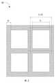
図1を参照すると、タッチスクリーン10の実施形態が、第1の静電容量式感知コンポーネント110、第1の接着剤層130、第2の静電容量式感知コンポーネント140、第2の接着剤層160、カバープレート170、及び回路基板180を含む。第1の静電容量式感知コンポーネント110は、第1の基板112及び第1のパターン化感知層114から成り、第2の静電容量式感知コンポーネント140は、第2の基板142及び第2のパターン化感知層144から成る。 Referring to FIG. 1, an embodiment of a
第1の基板112は、光学膜又はガラス板である。図示される実施形態において、第1の基板112は、ポリエチレンテレフタレート(PET)の材料で作製される。 The
第1のパターン化感知層114は、第1の基板112の表面上に形成される。 A first patterned sensing layer 114 is formed on the surface of the
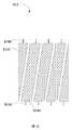
図2を参照すると、第1のパターン化感知層114は、第1の方向Xに沿って配列された複数の第1の感知電極1142を含む。第1の感知電極1142は、第1の基板112の表面上に配置された金属メッシュ20により作製される。 Referring to FIG. 2, the first patterned sensing layer 114 includes a plurality of
図3を参照すると、図示される実施形態において、金属メッシュ20は、銅、モリブデン−アルミニウム−モリブデン合金、又は銅−ニッケル合金で作製される。金属メッシュ20の酸化を避けるため、抗酸化層が金属メッシュ20の表面上に形成され、抗酸化層は、金、白金又はニッケル等のような不活性金属の材料で作製される。 Referring to FIG. 3, in the illustrated embodiment, the
金属メッシュ20の線幅(D)は、45nmより広い又はこれに等しく、かつ40000nmより狭いか又はこれに等しい。金属メッシュ20の線幅(D)は、タッチスクリーン10の解像度に影響を及ぼし、金属メッシュ20の線幅(D)が広すぎると、線が見えるため、タッチスクリーン10の解像度が影響を受け得ることに留意すべきである。金属メッシュ20の線幅(D)は、45nmより広いか又はこれに等しく、かつ、5000nmより狭いか又はこれに等しいことが好ましい。 The line width (D) of the
信号に対するタッチスクリーン10の感度を保証するために、金属メッシュ20の開口率(K)、第1の静電容量式感知コンポーネント110の透過率(T1)及び第1の基板112の透過率(T2)は、T1=T2*Kのように表される。従って、所望の条件を満たした金属メッシュ20の開口率は、第1の静電容量式感知コンポーネント110の設計透過率に従って計算することができる。In order to ensure the sensitivity of the
以下の金属メッシュ20を例にとると、金属メッシュ20のグリッドの形状は正方形である。金属メッシュ20の線幅はDであり、金属メッシュ20のグリッドの開口幅はLである。金属メッシュ20は、辺の長さがD+Lである複数のユニットセルから成るものと見なすことができ、金属メッシュ20の開口率(K)=ユニットセルの面積を金属メッシュ20の面積で割ったもの、である。具体的には、図示される実施形態において、K=L2/(L+D)2である。Taking the following
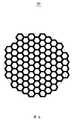
金属メッシュ20のグリッドは、図2に示した正方形に限られるものではなく、例えばそれぞれ図4乃至図6に示される、金属メッシュ30、金属メッシュ40及び金属メッシュ50のグリッドは、角柱形、三角形、又は六角形など、多角形であってもよいことに留意すべきである。 The grid of the
図2を参照すると、図示される実施形態において、第1の感知電極1142の各々は、順に接続された複数の感知ユニット1144及びワイヤ1146を含む。感知ユニット1144は、略角柱形であり、複数の感知ユニット1144は、第2の方向Yに沿って順に接続され、感知ユニット1144の1つの、2つの対向するコーナー部は、それぞれ2つの隣接する2つの感知ユニット1144のコーナー部に接続される。第1の基板114は略矩形であるため、2つの端部上の2つの感知ユニット1144は、切断のために三角形又は多角形であることに留意すべきである。 Referring to FIG. 2, in the illustrated embodiment, each of the
ワイヤ1146は、第1の感知電極1142の一端に配置された感知ユニット1144に電気的に接続される。図示される実施形態において、ワイヤ1146は金属ワイヤであり、ワイヤ1146及び該ワイヤ1146に接続された第1の感知電極1142は、一体化される。 The
図1を参照すると、第2の基板142は、第1の接着剤層130を介して第1のパターン化感知層114に接合される。第1の接着剤層130は、光学接着剤であり、具体的に、第1の接着剤層130の材料は、シリコーン又はアクリル接着剤である。アクリル接着剤は、アクリル接着剤及びメチルアクリル接着剤を含む。 Referring to FIG. 1, the
第2の基板142は、光学膜又はガラス板である。図示される実施形態において、第1の基板112の材料はPETである。第2の基板142のサイズは、第1の基板112のサイズより小さい。 The
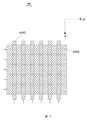
図2を参照すると、第2のパターン化感知層144は、第2の基板142の表面上に形成される。第2のパターン化感知層144は、第2の方向Yに配列された複数の第2の感知電極1442を含む。第2の感知電極1442は、第2の基板142上に配置された金属メッシュ20により作製される。図示される実施形態において、第2の感知電極1442の各々は、順に接続された複数の感知ユニット1444とワイヤ1446とを含む。感知ユニット1444は、略角柱形であり、複数の感知ユニット1444は、第1の方向Xに沿って順に接続される、つまり感知ユニット1444の1つの2つの対向するコーナー部は、それぞれ、2つの隣接する感知ユニット1444のコーナー部に接続される。第2の基板144は略矩形であるため、2つの端部にある2つの感知ユニット1444は、切断のために三角形又は多角形である。第2のパターン化感知層144の感知ユニット1444は、第1のパターン化感知層114の感知ユニット1144の隙間に対応する。 Referring to FIG. 2, the second
カバープレート170は、第2の接着剤層160を介して第2のパターン化感知層144に接合される。第2の接着剤層160は、光学接着剤であり、具体的には、第2の接着剤層160の材料は、シリコーン又はアクリル接着剤である。アクリル接着剤は、アクリル接着剤及びメチルアクリル接着剤を含む。 The
カバープレート170は、強化ガラス、ポリカーボネート(PC)、ポリメチルアクリレート(PMA)又はポリメチルメタクリレート(アクリル樹脂と略される)により形成された単層の板又は多層の複合板である。図示される実施形態において、カバープレート170のサイズは、第1の基板112のサイズとほぼ同じである。 The
回路基板180は、可撓性回路基板である。図示される実施形態において、回路基板180は、制御回路を有し、かつ、導電接着剤を介して、第1のパターン化感知層114の第1の感知電極1142のワイヤ1146及び第2のパターン化感知層144の第2の感知電極1142のワイヤ1446に電気的に接続される。導電接着剤は、異方性導電接着剤であることが好ましい。 The
タッチスクリーン10の第1のパターン化感知層114及び第2のパターン化感知層144は、金属メッシュで作製され、酸化インジウムスズを使用しないので、タッチスクリーン10の価格は低い。一方、金属メッシュの透過率は高い。 Since the first patterned sensing layer 114 and the second
図7を参照すると、別の実施形態のタッチスクリーン60の構造は、タッチスクリーン10のものとほぼ同じであり、違いは、タッチスクリーン60の第1の感知電極6142は、第2の方向Yに沿って延びる細長い棒であり、第2の感知電極6442は、第1の方向Xに沿って延びる細長いストリップであることである。図示される実施形態において、第1の感知電極6142の幅は、第2の感知電極6442の幅より狭い。 Referring to FIG. 7, the structure of the
第1の接着剤層130、並びに第2の基板142及び第2のパターン化感知層144からなる第2の静電容量式感知コンポーネント140を省略できることを理解すべきである。図8を参照すると、第1のパターン化感知層814は、複数の第1の感知電極8142及び複数の第2の感知電極8144を含む。第1の感知電極8142及び第2の感知電極8144は、直角三角形であり、第1の感知電極8142の形状及びサイズは、第2の感知電極8144の形状及びサイズと同じである。第1の感知電極8142及び第2の感知電極8144は、対で配置され、対で配置された第1の感知電極8142及び第2の感知電極8144の斜辺は、互いに対向する。第1の感知電極8142のより短い直角辺は、同一直線上にある。第2の感知電極8144のより短い直角辺は、同一直線上にある。図示される実施形態において、第1の感知電極8142及び第2の感知電極8144のより短い直角辺には、共にワイヤ8146が設けられる。図示される実施形態において、ワイヤ8146は金属ワイヤであり、ワイヤ8146及び第1の感知電極8142又は第2の感知電極8144は、一体化される。 It should be understood that the first
静電容量式感知コンポーネントの製造方法が、以下のステップを含む。:即ち、 A method of manufacturing a capacitive sensing component includes the following steps. :
S101:金属層が基板上に形成される。
図示される実施形態において、金属層は、真空蒸着又はマグネトロン・スパッタリングにより形成される。金属層は、銅、モリブデン−アルミニウム−モリブデン合金、又は銅−ニッケル合金で作製される。金属層の酸化を避けるため、真空蒸着又はマグネトロン・スパッタリングにより、抗酸化層が金属層の表面上に形成される。抗酸化層は、金、白金又はニッケル等のような不活性金属で作製される。S101: A metal layer is formed on the substrate.
In the illustrated embodiment, the metal layer is formed by vacuum evaporation or magnetron sputtering. The metal layer is made of copper, molybdenum-aluminum-molybdenum alloy, or copper-nickel alloy. In order to avoid oxidation of the metal layer, an antioxidant layer is formed on the surface of the metal layer by vacuum evaporation or magnetron sputtering. The antioxidant layer is made of an inert metal such as gold, platinum or nickel.
S102:金属層を、露光及び現像により処理して金属メッシュを形成し、さらに、金属メッシュを基板上に配列した複数の感知電極にパターン化する。従って、パターン化感知層は、基板上に形成される。 S102: The metal layer is processed by exposure and development to form a metal mesh, and further patterned into a plurality of sensing electrodes arranged on the substrate. Accordingly, the patterned sensing layer is formed on the substrate.
図示される実施形態において、パターン化感知層は、感知電極に対応して接続された複数のワイヤをさらに含み、ワイヤ及び対応する感知電極は一体化される。 In the illustrated embodiment, the patterned sensing layer further includes a plurality of wires connected corresponding to the sensing electrodes, and the wires and the corresponding sensing electrodes are integrated.
静電容量式感知コンポーネントのパターン化感知層は金属で作製され、価格は低い。さらに、露光及び現像により、ワイヤ及び対応する感知電極は一体化され、これは、高効率の処理方法である。 The patterned sensing layer of the capacitive sensing component is made of metal and is inexpensive. Furthermore, by exposure and development, the wires and corresponding sensing electrodes are integrated, which is a highly efficient processing method.
タッチスクリーン10の製造方法が、以下のステップを含む。 The manufacturing method of the
S901:第1の静電容量式感知コンポーネント110及び第2の静電容量式感知コンポーネント140を準備する。 S901: The first
図示される実施形態において、第1の静電容量式感知コンポーネント110の製造方法は、以下のステップを含む。:即ち、最初に、金属層を第1の基板112上に形成し、次いで、金属層を、露光及び現像により処理して金属メッシュ20を形成し、さらに金属メッシュ20をパターン化して、第1の基板112上に配列した複数の感知電極1142を形成し、かくしてパターン化感知層114が第1の基板112上に形成される。図示される実施形態において、第1の感知電極1142に接続されたワイヤ1146及び対応する第1の感知電極1142は、一体化される。 In the illustrated embodiment, the method of manufacturing the first
第2の静電容量式感知コンポーネント140の製造方法は、第1の静電容量式感知コンポーネント110の製造方法と同じであり、ここでは詳細に説明しない。 The method of manufacturing the second capacitive sensing component 140 is the same as the method of manufacturing the first
S902:第1の静電容量式感知コンポーネント110、第2の静電容量式感知コンポーネント140及びカバープレート170が、光学接着剤を介して順に接合される。 S902: The first
図示される実施形態において、光学接着剤の材料は、シリコーン又はアクリル接着剤である。アクリル接着剤は、アクリル接着剤及びメチルアクリル接着剤を含む。 In the illustrated embodiment, the optical adhesive material is a silicone or acrylic adhesive. The acrylic adhesive includes an acrylic adhesive and a methyl acrylic adhesive.
具体的には、第2の静電容量式感知コンポーネント140の第2の基板142は、第1の接着剤層130を介して、第1の静電容量式感知コンポーネント110の第1のパターン化感知層114に接合され、第1のパターン化感知層114の第1の感知電極1142は、第1の方向(X)に沿って配列され、第2のパターン化感知層144の第2の感知電極1442は、第2の方向(Y)に沿って配列される。カバープレート170は、第2の接着剤層160を介して、第2のパターン化感知層144に固定される。 Specifically, the
S903:第1の静電容量式感知コンポーネント110及び第2の静電容量式感知コンポーネント140は、回路基板180に電気的に接続される。 S903: The first
図示される実施形態において、回路基板180は、導電接着剤を介して、第1のパターン化感知層114の第1の感知電極1142のワイヤ1446及び第2のパターン化感知層144の第2の感知電極1442のワイヤ1446に接合され、従って、第1の静電容量式感知コンポーネント110及び第2の静電容量式感知コンポーネント140は、回路基板180に電気的に接続される。導電接着剤は、異方性導電接着剤であることが好ましい。 In the illustrated embodiment, the
静電容量式感知コンポーネント及びタッチスクリーン10の製造方法において、パターン化感知層は、金属で作製されるので価格が低く、ワイヤ及び対応する感知電極は、露光及び現像により一体化されるので、効率性が高い。 In the method of manufacturing the capacitive sensing component and the
第2の静電容量式感知コンポーネント120は省略することができ、その場合、第1の静電容量式感知コンポーネント110の第1のパターン化感知層114は、複数の第1の感知電極及び複数の第2の感知電極を含み、ステップS902において、カバープレート180は、光学接着剤を介して、第1の静電容量式感知コンポーネント110の第1のパターン化感知層114に接着される。 The second capacitive sensing component 120 can be omitted, in which case the first patterned sensing layer 114 of the first
実施例の説明は、具体的かつ詳細であるが、これらの説明は、本開示を限定するために用いてはならないことを理解すべきである。従って、本特許の保護の範囲は、添付の特許請求の範囲に従うべきである。 While the description of the examples is specific and detailed, it should be understood that these descriptions should not be used to limit the present disclosure. Accordingly, the scope of protection of this patent should be subject to the appended claims.
10、60:タッチスクリーン
20、30、40:金属メッシュ
110:第1の静電容量式感知コンポーネント
112:第1の基板
114、814:第1のパターン化感知層
130:第1の接着剤層
140:第2の静電容量式感知コンポーネント
142:第2の基板
144:第2のパターン化感知層
160:第2の接着剤層
160:第2の接着剤層
170:カバープレート
180:回路基板
1142、6142、8142:第1の感知電極
1442、6442、8144:第2の感知電極
1144、1444:感知ユニット
1146、8146:ワイヤ10, 60:
Claims (10)
Translated fromJapanese基板上に金属層を形成するステップと、
露光及び現像により、前記金属層を処理して金属メッシュを形成し、さらに前記金属メッシュをパターン化して前記基板上に配列された複数の感知電極にし、これにより前記基板上にパターン化感知層を形成するステップと、
を含むことを特徴とする方法。A method of manufacturing a capacitive sensing component, comprising:
Forming a metal layer on the substrate;
The metal layer is processed by exposure and development to form a metal mesh, and the metal mesh is further patterned to form a plurality of sensing electrodes arranged on the substrate, thereby forming a patterned sensing layer on the substrate. Forming step;
A method comprising the steps of:
前記静電容量式感知コンポーネントの前記パターン化感知層上に積層されたカバープレートと、
を含むことを特徴とするタッチスクリーン。The capacitive sensing component of claim 1;
A cover plate laminated on the patterned sensing layer of the capacitive sensing component;
A touch screen comprising:
Applications Claiming Priority (3)
| Application Number | Priority Date | Filing Date | Title |
|---|---|---|---|
| CN201210116195.7 | 2012-04-19 | ||
| CN2012101161957ACN103376958A (en) | 2012-04-19 | 2012-04-19 | Capacitive sensing component, preparing method thereof, and touch control screen with capacitive sensing component |
| PCT/CN2012/087082WO2013155852A1 (en) | 2012-04-19 | 2012-12-20 | Capacitive sensing module, manufacturing method therefor, and touch screen using capacitive sensing module |
Publications (2)
| Publication Number | Publication Date |
|---|---|
| JP2014514680Atrue JP2014514680A (en) | 2014-06-19 |
| JP5719476B2 JP5719476B2 (en) | 2015-05-20 |
Family
ID=49382870
Family Applications (1)
| Application Number | Title | Priority Date | Filing Date |
|---|---|---|---|
| JP2014510652AExpired - Fee RelatedJP5719476B2 (en) | 2012-04-19 | 2012-12-20 | Capacitive sensing component, method of manufacturing the same, and touch screen having capacitive sensing component |
Country Status (5)
| Country | Link |
|---|---|
| US (1) | US20140118009A1 (en) |
| JP (1) | JP5719476B2 (en) |
| KR (1) | KR20140066741A (en) |
| CN (1) | CN103376958A (en) |
| WO (1) | WO2013155852A1 (en) |
Cited By (1)
| Publication number | Priority date | Publication date | Assignee | Title |
|---|---|---|---|---|
| JP2020537199A (en)* | 2017-09-21 | 2020-12-17 | 京東方科技集團股▲ふん▼有限公司Boe Technology Group Co.,Ltd. | Touch panel and its manufacturing method, touch display panel |
Families Citing this family (6)
| Publication number | Priority date | Publication date | Assignee | Title |
|---|---|---|---|---|
| KR102187929B1 (en)* | 2013-11-22 | 2020-12-07 | 엘지이노텍 주식회사 | Touch window and display with the same |
| KR101512568B1 (en)* | 2013-12-24 | 2015-04-15 | 삼성전기주식회사 | Touch panel and touchscreen apparatus including the same |
| WO2015113395A1 (en)* | 2014-01-30 | 2015-08-06 | Zheng Shi | System and method for directing a moving object on an interactive surface |
| JP6009488B2 (en)* | 2014-03-28 | 2016-10-19 | 富士フイルム株式会社 | Sheet-like conductor and touch panel using the same |
| KR102154216B1 (en)* | 2017-09-18 | 2020-09-09 | 주식회사 아모그린텍 | Substrate for touch screen panel, touch screen panel having the same and manufacturing method thereof |
| US11360628B2 (en)* | 2020-06-23 | 2022-06-14 | Wuhan China Star Optoelectronics Semiconductor Display Technology Co., Ltd. | Self-capacitive touch substrate and display device |
Citations (5)
| Publication number | Priority date | Publication date | Assignee | Title |
|---|---|---|---|---|
| JP2010039537A (en)* | 2008-07-31 | 2010-02-18 | Gunze Ltd | Touch panel |
| JP2010160745A (en)* | 2009-01-09 | 2010-07-22 | Dainippon Printing Co Ltd | Color filter and display |
| JP2012014669A (en)* | 2009-11-20 | 2012-01-19 | Fujifilm Corp | Conductive sheet, method of using conductive sheet and electrostatic capacitive touch panel |
| JP2012053644A (en)* | 2010-08-31 | 2012-03-15 | Fujifilm Corp | Conductive sheet, method for using conductive sheet and capacitance system touch panel |
| WO2012043189A1 (en)* | 2010-09-29 | 2012-04-05 | 大日本印刷株式会社 | Touch panel sensor film and method for manufacturing same |
Family Cites Families (15)
| Publication number | Priority date | Publication date | Assignee | Title |
|---|---|---|---|---|
| US7663607B2 (en)* | 2004-05-06 | 2010-02-16 | Apple Inc. | Multipoint touchscreen |
| CN102981678B (en)* | 2006-06-09 | 2015-07-22 | 苹果公司 | Touch screen liquid crystal display |
| JP2009259063A (en)* | 2008-04-18 | 2009-11-05 | Gunze Ltd | Touch panel and its production method |
| WO2010013679A1 (en)* | 2008-07-31 | 2010-02-04 | グンゼ株式会社 | Planar element, and touch switch |
| US9244568B2 (en)* | 2008-11-15 | 2016-01-26 | Atmel Corporation | Touch screen sensor |
| CN101577148B (en)* | 2009-06-23 | 2012-11-07 | 中国乐凯胶片集团公司 | Transparent conducting film and preparation method thereof |
| WO2011002617A1 (en)* | 2009-06-30 | 2011-01-06 | 3M Innovative Properties Company | Electronic displays and metal micropatterned substrates having a graphic |
| TWI438671B (en)* | 2009-09-02 | 2014-05-21 | Mstar Semiconductor Inc | Touch sensing module, display apparatus and manufacturing method thereof |
| CN101655759B (en)* | 2009-09-22 | 2012-07-04 | 友达光电股份有限公司 | touch display panel |
| US8593413B2 (en)* | 2010-03-01 | 2013-11-26 | Cando Corporation | Sensory structure of capacitive touch panel and capacitive touch panel having the same |
| KR101048913B1 (en)* | 2010-04-01 | 2011-07-12 | 삼성모바일디스플레이주식회사 | Touch screen panel |
| US8941395B2 (en)* | 2010-04-27 | 2015-01-27 | 3M Innovative Properties Company | Integrated passive circuit elements for sensing devices |
| CN101968697B (en)* | 2010-08-13 | 2015-12-16 | 牧东光电(苏州)有限公司 | The method of manufacture grid pattern type contact panel |
| CN101976146B (en)* | 2010-10-12 | 2012-05-30 | 友达光电股份有限公司 | Manufacturing method of touch panel |
| WO2013155854A1 (en)* | 2012-04-19 | 2013-10-24 | 深圳欧菲光科技股份有限公司 | Electrically conductive component and manufacturing method therefor |
- 2012
- 2012-04-19CNCN2012101161957Apatent/CN103376958A/enactivePending
- 2012-12-20JPJP2014510652Apatent/JP5719476B2/ennot_activeExpired - Fee Related
- 2012-12-20KRKR1020147008151Apatent/KR20140066741A/ennot_activeCeased
- 2012-12-20WOPCT/CN2012/087082patent/WO2013155852A1/enactiveApplication Filing
- 2012-12-20USUS14/000,163patent/US20140118009A1/ennot_activeAbandoned
Patent Citations (5)
| Publication number | Priority date | Publication date | Assignee | Title |
|---|---|---|---|---|
| JP2010039537A (en)* | 2008-07-31 | 2010-02-18 | Gunze Ltd | Touch panel |
| JP2010160745A (en)* | 2009-01-09 | 2010-07-22 | Dainippon Printing Co Ltd | Color filter and display |
| JP2012014669A (en)* | 2009-11-20 | 2012-01-19 | Fujifilm Corp | Conductive sheet, method of using conductive sheet and electrostatic capacitive touch panel |
| JP2012053644A (en)* | 2010-08-31 | 2012-03-15 | Fujifilm Corp | Conductive sheet, method for using conductive sheet and capacitance system touch panel |
| WO2012043189A1 (en)* | 2010-09-29 | 2012-04-05 | 大日本印刷株式会社 | Touch panel sensor film and method for manufacturing same |
Cited By (1)
| Publication number | Priority date | Publication date | Assignee | Title |
|---|---|---|---|---|
| JP2020537199A (en)* | 2017-09-21 | 2020-12-17 | 京東方科技集團股▲ふん▼有限公司Boe Technology Group Co.,Ltd. | Touch panel and its manufacturing method, touch display panel |
Also Published As
| Publication number | Publication date |
|---|---|
| KR20140066741A (en) | 2014-06-02 |
| JP5719476B2 (en) | 2015-05-20 |
| US20140118009A1 (en) | 2014-05-01 |
| WO2013155852A1 (en) | 2013-10-24 |
| CN103376958A (en) | 2013-10-30 |
Similar Documents
| Publication | Publication Date | Title |
|---|---|---|
| JP5719476B2 (en) | Capacitive sensing component, method of manufacturing the same, and touch screen having capacitive sensing component | |
| JP3192251U (en) | Touch panel and touch display device | |
| JP5849340B2 (en) | Touch screen sensing module, manufacturing method thereof, and display device | |
| CN109871157B (en) | Touch display panel and touch display device | |
| JP5734828B2 (en) | Structural material for touch panel and touch panel structure | |
| CN103186287B (en) | A kind of touching display screen and touch control display apparatus | |
| JP5914925B2 (en) | Touch panel | |
| US10496232B2 (en) | Capacitive touch panel | |
| JP5887642B2 (en) | Conductive film, method for manufacturing the same, and touch screen including the conductive film | |
| EP3683661A1 (en) | Touch panel and manufacturing method thereof, and touch display device | |
| TW201337680A (en) | Input device | |
| CN104182101B (en) | Touch display panel and touch display device | |
| JP2013178738A (en) | Input device | |
| CN108073335A (en) | Touch panel | |
| KR20140137282A (en) | Capacitive transparent conductive film and preparation method thereof | |
| JP6047420B2 (en) | Capacitance switch and manufacturing method thereof | |
| CN203178979U (en) | Touch screen induction module and display with same | |
| US9538654B2 (en) | Conductive film, method for manufacturing the same, and touch screen including the same | |
| JP5734799B2 (en) | Structural material for touch panel and touch panel structure | |
| CN103809797A (en) | Touch electrode device | |
| JP2014513845A (en) | Conductive component and preparation method thereof | |
| CN203643969U (en) | A kind of touch substrate, touch screen and display device | |
| US9089061B2 (en) | Conductive film, method for making the same, and touch screen including the same | |
| CN202632261U (en) | Capacitive sensing component and touch screen employing same | |
| CN103472969A (en) | Capacitive touch screen |
Legal Events
| Date | Code | Title | Description |
|---|---|---|---|
| A621 | Written request for application examination | Free format text:JAPANESE INTERMEDIATE CODE: A621 Effective date:20131113 | |
| A131 | Notification of reasons for refusal | Free format text:JAPANESE INTERMEDIATE CODE: A131 Effective date:20140901 | |
| A521 | Request for written amendment filed | Free format text:JAPANESE INTERMEDIATE CODE: A523 Effective date:20141121 | |
| A131 | Notification of reasons for refusal | Free format text:JAPANESE INTERMEDIATE CODE: A131 Effective date:20150107 | |
| A521 | Request for written amendment filed | Free format text:JAPANESE INTERMEDIATE CODE: A523 Effective date:20150127 | |
| TRDD | Decision of grant or rejection written | ||
| A01 | Written decision to grant a patent or to grant a registration (utility model) | Free format text:JAPANESE INTERMEDIATE CODE: A01 Effective date:20150218 | |
| A61 | First payment of annual fees (during grant procedure) | Free format text:JAPANESE INTERMEDIATE CODE: A61 Effective date:20150320 | |
| R150 | Certificate of patent or registration of utility model | Ref document number:5719476 Country of ref document:JP Free format text:JAPANESE INTERMEDIATE CODE: R150 | |
| R250 | Receipt of annual fees | Free format text:JAPANESE INTERMEDIATE CODE: R250 | |
| LAPS | Cancellation because of no payment of annual fees |