JP2014507011A - Glassy polymer antireflection film, production method, and light energy absorption device using the film - Google Patents
Glassy polymer antireflection film, production method, and light energy absorption device using the filmDownload PDFInfo
- Publication number
- JP2014507011A JP2014507011AJP2013543221AJP2013543221AJP2014507011AJP 2014507011 AJP2014507011 AJP 2014507011AJP 2013543221 AJP2013543221 AJP 2013543221AJP 2013543221 AJP2013543221 AJP 2013543221AJP 2014507011 AJP2014507011 AJP 2014507011A
- Authority
- JP
- Japan
- Prior art keywords
- light
- structured
- film
- antireflective
- light energy
- Prior art date
- Legal status (The legal status is an assumption and is not a legal conclusion. Google has not performed a legal analysis and makes no representation as to the accuracy of the status listed.)
- Pending
Links
- 238000004519manufacturing processMethods0.000titleclaimsdescription19
- 238000010521absorption reactionMethods0.000titleabstractdescription22
- 229920000642polymerPolymers0.000titledescription5
- 230000003667anti-reflective effectEffects0.000claimsabstractdescription122
- 239000006096absorbing agentSubstances0.000claimsabstractdescription52
- 239000000758substrateSubstances0.000claimsabstractdescription45
- 229910004298SiO 2Inorganic materials0.000claimsabstractdescription29
- 239000000463materialSubstances0.000claimsdescription89
- 229920002379silicone rubberPolymers0.000claimsdescription77
- QVGXLLKOCUKJST-UHFFFAOYSA-Natomic oxygenChemical compound[O]QVGXLLKOCUKJST-UHFFFAOYSA-N0.000claimsdescription18
- 229910052760oxygenInorganic materials0.000claimsdescription18
- 239000001301oxygenSubstances0.000claimsdescription18
- 238000000034methodMethods0.000claimsdescription16
- 125000004432carbon atomChemical groupC*0.000claimsdescription5
- 230000008569processEffects0.000claimsdescription5
- CBENFWSGALASAD-UHFFFAOYSA-NOzoneChemical compound[O-][O+]=OCBENFWSGALASAD-UHFFFAOYSA-N0.000claimsdescription4
- 230000005855radiationEffects0.000claimsdescription3
- 229920001296polysiloxanePolymers0.000abstractdescription34
- 239000013536elastomeric materialSubstances0.000abstractdescription2
- 239000010408filmSubstances0.000description178
- 238000012360testing methodMethods0.000description84
- VYPSYNLAJGMNEJ-UHFFFAOYSA-NSilicium dioxideChemical compoundO=[Si]=OVYPSYNLAJGMNEJ-UHFFFAOYSA-N0.000description73
- 238000002834transmittanceMethods0.000description57
- 239000004576sandSubstances0.000description33
- 238000001179sorption measurementMethods0.000description28
- 239000002689soilSubstances0.000description27
- 230000005540biological transmissionEffects0.000description24
- 239000002243precursorSubstances0.000description23
- 238000010894electron beam technologyMethods0.000description21
- 239000011521glassSubstances0.000description19
- 230000001965increasing effectEffects0.000description18
- 239000002245particleSubstances0.000description16
- 230000004888barrier functionEffects0.000description14
- 229920000139polyethylene terephthalatePolymers0.000description14
- 239000005020polyethylene terephthalateSubstances0.000description14
- 239000008119colloidal silicaSubstances0.000description12
- XLYOFNOQVPJJNP-UHFFFAOYSA-NwaterSubstancesOXLYOFNOQVPJJNP-UHFFFAOYSA-N0.000description12
- -1polydimethylsiloxanePolymers0.000description10
- 239000011248coating agentSubstances0.000description9
- 238000000576coating methodMethods0.000description9
- 238000004132cross linkingMethods0.000description9
- IJGRMHOSHXDMSA-UHFFFAOYSA-NAtomic nitrogenChemical compoundN#NIJGRMHOSHXDMSA-UHFFFAOYSA-N0.000description8
- 239000000203mixtureSubstances0.000description8
- 239000004447silicone coatingSubstances0.000description8
- 229920002799BoPETPolymers0.000description7
- XUIMIQQOPSSXEZ-UHFFFAOYSA-NSiliconChemical compound[Si]XUIMIQQOPSSXEZ-UHFFFAOYSA-N0.000description7
- 239000000428dustSubstances0.000description7
- 239000000377silicon dioxideSubstances0.000description7
- 230000003068static effectEffects0.000description7
- 229920003229poly(methyl methacrylate)Polymers0.000description6
- 229910052710siliconInorganic materials0.000description6
- 239000010703siliconSubstances0.000description6
- 230000005611electricityEffects0.000description5
- 238000010438heat treatmentMethods0.000description5
- 230000014759maintenance of locationEffects0.000description5
- 239000011295pitchSubstances0.000description5
- 238000012545processingMethods0.000description5
- 239000004743PolypropyleneSubstances0.000description4
- 229910020175SiOHInorganic materials0.000description4
- GWEVSGVZZGPLCZ-UHFFFAOYSA-NTitan oxideChemical compoundO=[Ti]=OGWEVSGVZZGPLCZ-UHFFFAOYSA-N0.000description4
- MCMNRKCIXSYSNV-UHFFFAOYSA-NZirconium dioxideChemical compoundO=[Zr]=OMCMNRKCIXSYSNV-UHFFFAOYSA-N0.000description4
- 230000008901benefitEffects0.000description4
- 230000008859changeEffects0.000description4
- 238000006243chemical reactionMethods0.000description4
- 239000002105nanoparticleSubstances0.000description4
- 229910052757nitrogenInorganic materials0.000description4
- 238000009832plasma treatmentMethods0.000description4
- 239000002033PVDF binderSubstances0.000description3
- 230000001133accelerationEffects0.000description3
- 239000000853adhesiveSubstances0.000description3
- 230000001070adhesive effectEffects0.000description3
- 239000012298atmosphereSubstances0.000description3
- 239000004205dimethyl polysiloxaneSubstances0.000description3
- 238000005516engineering processMethods0.000description3
- 229910052739hydrogenInorganic materials0.000description3
- 230000003287optical effectEffects0.000description3
- 229920000435poly(dimethylsiloxane)Polymers0.000description3
- 229920002981polyvinylidene fluoridePolymers0.000description3
- 238000003860storageMethods0.000description3
- 229920001187thermosetting polymerPolymers0.000description3
- 239000004812Fluorinated ethylene propyleneSubstances0.000description2
- 229920002274NalgenePolymers0.000description2
- 229910018540Si CInorganic materials0.000description2
- 229920004482WACKER®Polymers0.000description2
- 238000005299abrasionMethods0.000description2
- 239000002390adhesive tapeSubstances0.000description2
- 229910052782aluminiumInorganic materials0.000description2
- XAGFODPZIPBFFR-UHFFFAOYSA-NaluminiumChemical compound[Al]XAGFODPZIPBFFR-UHFFFAOYSA-N0.000description2
- 230000015556catabolic processEffects0.000description2
- 229910010293ceramic materialInorganic materials0.000description2
- 230000006378damageEffects0.000description2
- 238000006731degradation reactionMethods0.000description2
- 230000007613environmental effectEffects0.000description2
- 239000004744fabricSubstances0.000description2
- 239000002657fibrous materialSubstances0.000description2
- 239000007789gasSubstances0.000description2
- 230000006698inductionEffects0.000description2
- 239000011368organic materialSubstances0.000description2
- 229920009441perflouroethylene propylenePolymers0.000description2
- 239000013500performance materialSubstances0.000description2
- 238000001020plasma etchingMethods0.000description2
- 229920001155polypropylenePolymers0.000description2
- 229920002635polyurethanePolymers0.000description2
- 239000004814polyurethaneSubstances0.000description2
- 238000010248power generationMethods0.000description2
- 230000002035prolonged effectEffects0.000description2
- 238000010926purgeMethods0.000description2
- 239000010453quartzSubstances0.000description2
- 150000003839saltsChemical class0.000description2
- 229910010271silicon carbideInorganic materials0.000description2
- 238000004381surface treatmentMethods0.000description2
- 239000010409thin filmSubstances0.000description2
- LEVFXWNQQSSNAC-UHFFFAOYSA-N2-(4,6-diphenyl-1,3,5-triazin-2-yl)-5-hexoxyphenolChemical compoundOC1=CC(OCCCCCC)=CC=C1C1=NC(C=2C=CC=CC=2)=NC(C=2C=CC=CC=2)=N1LEVFXWNQQSSNAC-UHFFFAOYSA-N0.000description1
- NIXOWILDQLNWCW-UHFFFAOYSA-MAcrylateChemical compound[O-]C(=O)C=CNIXOWILDQLNWCW-UHFFFAOYSA-M0.000description1
- 101100008050Caenorhabditis elegans cut-6 geneProteins0.000description1
- RYGMFSIKBFXOCR-UHFFFAOYSA-NCopperChemical compound[Cu]RYGMFSIKBFXOCR-UHFFFAOYSA-N0.000description1
- 241000218691CupressaceaeSpecies0.000description1
- MYMOFIZGZYHOMD-UHFFFAOYSA-NDioxygenChemical compoundO=OMYMOFIZGZYHOMD-UHFFFAOYSA-N0.000description1
- VGGSQFUCUMXWEO-UHFFFAOYSA-NEtheneChemical compoundC=CVGGSQFUCUMXWEO-UHFFFAOYSA-N0.000description1
- 239000005977EthyleneSubstances0.000description1
- GYHNNYVSQQEPJS-UHFFFAOYSA-NGalliumChemical compound[Ga]GYHNNYVSQQEPJS-UHFFFAOYSA-N0.000description1
- OWYWGLHRNBIFJP-UHFFFAOYSA-NIpazineChemical compoundCCN(CC)C1=NC(Cl)=NC(NC(C)C)=N1OWYWGLHRNBIFJP-UHFFFAOYSA-N0.000description1
- 229920009405Polyvinylidenefluoride (PVDF) FilmPolymers0.000description1
- BUGBHKTXTAQXES-UHFFFAOYSA-NSeleniumChemical compound[Se]BUGBHKTXTAQXES-UHFFFAOYSA-N0.000description1
- BLRPTPMANUNPDV-UHFFFAOYSA-NSilaneChemical compound[SiH4]BLRPTPMANUNPDV-UHFFFAOYSA-N0.000description1
- 238000013459approachMethods0.000description1
- 238000007664blowingMethods0.000description1
- 239000003795chemical substances by applicationSubstances0.000description1
- 239000003245coalSubstances0.000description1
- 238000002485combustion reactionMethods0.000description1
- 238000009833condensationMethods0.000description1
- 230000005494condensationEffects0.000description1
- 229910052802copperInorganic materials0.000description1
- 239000010949copperSubstances0.000description1
- 238000003851corona treatmentMethods0.000description1
- 239000013078crystalSubstances0.000description1
- 230000007423decreaseEffects0.000description1
- 230000006866deteriorationEffects0.000description1
- 229910001882dioxygenInorganic materials0.000description1
- 239000006185dispersionSubstances0.000description1
- 238000009826distributionMethods0.000description1
- 230000000694effectsEffects0.000description1
- 230000002708enhancing effectEffects0.000description1
- 229920000840ethylene tetrafluoroethylene copolymerPolymers0.000description1
- 239000012530fluidSubstances0.000description1
- 239000002803fossil fuelSubstances0.000description1
- 229910052733galliumInorganic materials0.000description1
- 239000005431greenhouse gasSubstances0.000description1
- 229910052738indiumInorganic materials0.000description1
- APFVFJFRJDLVQX-UHFFFAOYSA-Nindium atomChemical compound[In]APFVFJFRJDLVQX-UHFFFAOYSA-N0.000description1
- 229910010272inorganic materialInorganic materials0.000description1
- 239000011147inorganic materialSubstances0.000description1
- 239000010954inorganic particleSubstances0.000description1
- 238000010030laminatingMethods0.000description1
- 230000007774longtermEffects0.000description1
- 238000002156mixingMethods0.000description1
- 238000012986modificationMethods0.000description1
- 230000004048modificationEffects0.000description1
- 239000003607modifierSubstances0.000description1
- 239000003921oilSubstances0.000description1
- 230000003647oxidationEffects0.000description1
- 238000007254oxidation reactionMethods0.000description1
- 230000035515penetrationEffects0.000description1
- 229920003023plasticPolymers0.000description1
- 239000004033plasticSubstances0.000description1
- 229920006289polycarbonate filmPolymers0.000description1
- 239000004926polymethyl methacrylateSubstances0.000description1
- 229920006264polyurethane filmPolymers0.000description1
- 239000000843powderSubstances0.000description1
- 230000001105regulatory effectEffects0.000description1
- 238000012827research and developmentMethods0.000description1
- 229920005989resinPolymers0.000description1
- 239000011347resinSubstances0.000description1
- 230000004044responseEffects0.000description1
- 229920002631room-temperature vulcanizate siliconePolymers0.000description1
- 229910052711seleniumInorganic materials0.000description1
- 239000011669seleniumSubstances0.000description1
- 229910000077silaneInorganic materials0.000description1
- 239000004945silicone rubberSubstances0.000description1
- 239000007787solidSubstances0.000description1
- 238000010998test methodMethods0.000description1
- 229920001169thermoplasticPolymers0.000description1
- 229920005992thermoplastic resinPolymers0.000description1
- 239000004416thermosoftening plasticSubstances0.000description1
- 239000013306transparent fiberSubstances0.000description1
- 229940124543ultraviolet light absorberDrugs0.000description1
Images


Classifications
- F—MECHANICAL ENGINEERING; LIGHTING; HEATING; WEAPONS; BLASTING
- F24—HEATING; RANGES; VENTILATING
- F24S—SOLAR HEAT COLLECTORS; SOLAR HEAT SYSTEMS
- F24S80/00—Details, accessories or component parts of solar heat collectors not provided for in groups F24S10/00-F24S70/00
- F24S80/50—Elements for transmitting incoming solar rays and preventing outgoing heat radiation; Transparent coverings
- F24S80/52—Elements for transmitting incoming solar rays and preventing outgoing heat radiation; Transparent coverings characterised by the material
- F—MECHANICAL ENGINEERING; LIGHTING; HEATING; WEAPONS; BLASTING
- F24—HEATING; RANGES; VENTILATING
- F24S—SOLAR HEAT COLLECTORS; SOLAR HEAT SYSTEMS
- F24S70/00—Details of absorbing elements
- F24S70/30—Auxiliary coatings, e.g. anti-reflective coatings
- G—PHYSICS
- G02—OPTICS
- G02B—OPTICAL ELEMENTS, SYSTEMS OR APPARATUS
- G02B1/00—Optical elements characterised by the material of which they are made; Optical coatings for optical elements
- G02B1/10—Optical coatings produced by application to, or surface treatment of, optical elements
- G02B1/11—Anti-reflection coatings
- G02B1/118—Anti-reflection coatings having sub-optical wavelength surface structures designed to provide an enhanced transmittance, e.g. moth-eye structures
- G—PHYSICS
- G02—OPTICS
- G02B—OPTICAL ELEMENTS, SYSTEMS OR APPARATUS
- G02B1/00—Optical elements characterised by the material of which they are made; Optical coatings for optical elements
- G02B1/10—Optical coatings produced by application to, or surface treatment of, optical elements
- G02B1/12—Optical coatings produced by application to, or surface treatment of, optical elements by surface treatment, e.g. by irradiation
- G—PHYSICS
- G02—OPTICS
- G02B—OPTICAL ELEMENTS, SYSTEMS OR APPARATUS
- G02B27/00—Optical systems or apparatus not provided for by any of the groups G02B1/00 - G02B26/00, G02B30/00
- G—PHYSICS
- G02—OPTICS
- G02B—OPTICAL ELEMENTS, SYSTEMS OR APPARATUS
- G02B27/00—Optical systems or apparatus not provided for by any of the groups G02B1/00 - G02B26/00, G02B30/00
- G02B27/0006—Optical systems or apparatus not provided for by any of the groups G02B1/00 - G02B26/00, G02B30/00 with means to keep optical surfaces clean, e.g. by preventing or removing dirt, stains, contamination, condensation
- G—PHYSICS
- G02—OPTICS
- G02B—OPTICAL ELEMENTS, SYSTEMS OR APPARATUS
- G02B5/00—Optical elements other than lenses
- G02B5/02—Diffusing elements; Afocal elements
- G02B5/0205—Diffusing elements; Afocal elements characterised by the diffusing properties
- G02B5/021—Diffusing elements; Afocal elements characterised by the diffusing properties the diffusion taking place at the element's surface, e.g. by means of surface roughening or microprismatic structures
- H—ELECTRICITY
- H10—SEMICONDUCTOR DEVICES; ELECTRIC SOLID-STATE DEVICES NOT OTHERWISE PROVIDED FOR
- H10F—INORGANIC SEMICONDUCTOR DEVICES SENSITIVE TO INFRARED RADIATION, LIGHT, ELECTROMAGNETIC RADIATION OF SHORTER WAVELENGTH OR CORPUSCULAR RADIATION
- H10F77/00—Constructional details of devices covered by this subclass
- H10F77/40—Optical elements or arrangements
- H10F77/42—Optical elements or arrangements directly associated or integrated with photovoltaic cells, e.g. light-reflecting means or light-concentrating means
- H—ELECTRICITY
- H10—SEMICONDUCTOR DEVICES; ELECTRIC SOLID-STATE DEVICES NOT OTHERWISE PROVIDED FOR
- H10F—INORGANIC SEMICONDUCTOR DEVICES SENSITIVE TO INFRARED RADIATION, LIGHT, ELECTROMAGNETIC RADIATION OF SHORTER WAVELENGTH OR CORPUSCULAR RADIATION
- H10F77/00—Constructional details of devices covered by this subclass
- H10F77/60—Arrangements for cooling, heating, ventilating or compensating for temperature fluctuations
- H10F77/63—Arrangements for cooling directly associated or integrated with photovoltaic cells, e.g. heat sinks directly associated with the photovoltaic cells or integrated Peltier elements for active cooling
- H—ELECTRICITY
- H10—SEMICONDUCTOR DEVICES; ELECTRIC SOLID-STATE DEVICES NOT OTHERWISE PROVIDED FOR
- H10F—INORGANIC SEMICONDUCTOR DEVICES SENSITIVE TO INFRARED RADIATION, LIGHT, ELECTROMAGNETIC RADIATION OF SHORTER WAVELENGTH OR CORPUSCULAR RADIATION
- H10F77/00—Constructional details of devices covered by this subclass
- H10F77/70—Surface textures, e.g. pyramid structures
- H10F77/707—Surface textures, e.g. pyramid structures of the substrates or of layers on substrates, e.g. textured ITO layer on a glass substrate
- Y—GENERAL TAGGING OF NEW TECHNOLOGICAL DEVELOPMENTS; GENERAL TAGGING OF CROSS-SECTIONAL TECHNOLOGIES SPANNING OVER SEVERAL SECTIONS OF THE IPC; TECHNICAL SUBJECTS COVERED BY FORMER USPC CROSS-REFERENCE ART COLLECTIONS [XRACs] AND DIGESTS
- Y02—TECHNOLOGIES OR APPLICATIONS FOR MITIGATION OR ADAPTATION AGAINST CLIMATE CHANGE
- Y02E—REDUCTION OF GREENHOUSE GAS [GHG] EMISSIONS, RELATED TO ENERGY GENERATION, TRANSMISSION OR DISTRIBUTION
- Y02E10/00—Energy generation through renewable energy sources
- Y02E10/40—Solar thermal energy, e.g. solar towers
- Y—GENERAL TAGGING OF NEW TECHNOLOGICAL DEVELOPMENTS; GENERAL TAGGING OF CROSS-SECTIONAL TECHNOLOGIES SPANNING OVER SEVERAL SECTIONS OF THE IPC; TECHNICAL SUBJECTS COVERED BY FORMER USPC CROSS-REFERENCE ART COLLECTIONS [XRACs] AND DIGESTS
- Y02—TECHNOLOGIES OR APPLICATIONS FOR MITIGATION OR ADAPTATION AGAINST CLIMATE CHANGE
- Y02E—REDUCTION OF GREENHOUSE GAS [GHG] EMISSIONS, RELATED TO ENERGY GENERATION, TRANSMISSION OR DISTRIBUTION
- Y02E10/00—Energy generation through renewable energy sources
- Y02E10/50—Photovoltaic [PV] energy
- Y02E10/52—PV systems with concentrators
- Y—GENERAL TAGGING OF NEW TECHNOLOGICAL DEVELOPMENTS; GENERAL TAGGING OF CROSS-SECTIONAL TECHNOLOGIES SPANNING OVER SEVERAL SECTIONS OF THE IPC; TECHNICAL SUBJECTS COVERED BY FORMER USPC CROSS-REFERENCE ART COLLECTIONS [XRACs] AND DIGESTS
- Y10—TECHNICAL SUBJECTS COVERED BY FORMER USPC
- Y10T—TECHNICAL SUBJECTS COVERED BY FORMER US CLASSIFICATION
- Y10T156/00—Adhesive bonding and miscellaneous chemical manufacture
- Y10T156/10—Methods of surface bonding and/or assembly therefor
Landscapes
- Physics & Mathematics (AREA)
- Engineering & Computer Science (AREA)
- Optics & Photonics (AREA)
- General Physics & Mathematics (AREA)
- Chemical & Material Sciences (AREA)
- Thermal Sciences (AREA)
- Sustainable Energy (AREA)
- Combustion & Propulsion (AREA)
- Mechanical Engineering (AREA)
- General Engineering & Computer Science (AREA)
- Sustainable Development (AREA)
- Life Sciences & Earth Sciences (AREA)
- Laminated Bodies (AREA)
- Photovoltaic Devices (AREA)
- Surface Treatment Of Optical Elements (AREA)
Abstract
Translated fromJapaneseDescription
Translated fromJapanese (関連出願の相互参照)
本出願は2010年12月8日出願の米国特許仮出願第61/421047号の利益を主張するものであり、その全容は参照により本明細書に組み込まれる。(Cross-reference of related applications)
This application claims the benefit of US Provisional Application No. 61 / 421,647, filed Dec. 8, 2010, which is incorporated herein by reference in its entirety.
本発明は、透明反射防止構造化フィルム、特に架橋シリコーンエラストマー材を含む透明反射防止構造化フィルム、より詳細には、ガラス状表面を有する反射防止構造体を含むそのようなフィルム、そのようなフィルムの製造方法、及びそのようなフィルムを備えた光エネルギー吸収装置に関する。 The present invention relates to a transparent antireflective structured film, in particular a transparent antireflective structured film comprising a crosslinked silicone elastomer material, more particularly such a film comprising an antireflective structure having a glassy surface, such a film. And a light energy absorbing device provided with such a film.
従来の化石燃料の燃焼に基づく発電(例えば、石油及び石炭に頼った発電所)のコストの上昇、及びこれにともなう温室効果ガスを低減する必要から、従来とは異なる電力の供給源に対する投資が増大している。例えば、米国エネルギー省は、太陽光発電の研究開発に多大な投資を行ってきた(例えば、太陽光エネルギーに基づいた温水及び電力の発生)。このような従来とは異なる発電の供給源の1つとして、太陽光エネルギーを電力に変換する光電池の使用がある。太陽光エネルギーは、住宅用及び商業用の温水を直接的又は間接的に加熱する目的でも使用されている。このような関心の高まりとともに、従来とは異なるこうした太陽光エネルギー技術による光エネルギーの吸収効率を高め、これにより利用可能な太陽光エネルギーの量を増大させることが求められている。 Because of the increased cost of power generation based on the combustion of conventional fossil fuels (for example, power plants that rely on oil and coal) and the need to reduce greenhouse gases, there is a need to invest in different power sources. It is increasing. For example, the US Department of Energy has made significant investments in solar power research and development (eg, generation of hot water and electricity based on solar energy). One of the power supply sources different from the conventional one is the use of a photovoltaic cell that converts solar energy into electric power. Solar energy is also used for the purpose of directly or indirectly heating residential and commercial hot water. Along with such an increase in interest, there is a need to increase the amount of solar energy that can be used by increasing the absorption efficiency of light energy by such a different solar energy technology.
本発明は、より有用な光エネルギーを該当する光吸収要素(例えば、光電池)に与えることによって、太陽光エネルギー及び他の光エネルギー吸収技術の効率を高める(即ち、エネルギー発生能力を高める)手段を提供するものである。 The present invention provides a means for increasing the efficiency of solar energy and other light energy absorption technologies (ie, increasing the ability to generate energy) by providing more useful light energy to the appropriate light absorbing elements (eg, photovoltaic cells). It is to provide.
シリコーンエラストマーは、長期の紫外線曝露下におけるその安定性によって知られ、光学的に透明かつ強靱であり得る。残念なことに、シリコーンエラストマーは、汚れ及び埃の粒子を誘引、吸着及び保持する傾向を有する比較的粘着性の表面を有してもいる。これまで、汚れ及び埃を吸着及び保持するこうした特性のため、シリコーンエラストマーは、例えば光電池用の光学的に透明な角柱状カバーなどの光エネルギー吸収又は変換装置の露出表面を形成するための候補としては望ましくないものであった。本発明は、少なくとも部分的に、シリコーンエラストマー材の構造化表面を、化学量論的量のSiO2を含むガラス状表面となるように処理することによって、シリコーンエラストマー表面のこの粘着性が有意に低減され、またそれらの汚れ及び埃粒子の吸着に対する耐性が有意に増大され得るという発見に基づくものである。Silicone elastomers are known for their stability under prolonged UV exposure and can be optically clear and tough. Unfortunately, silicone elastomers also have a relatively sticky surface that tends to attract, adsorb and retain dirt and dust particles. So far, because of these properties of adsorbing and retaining dirt and dust, silicone elastomers are candidates for forming exposed surfaces of light energy absorption or conversion devices, such as optically transparent prismatic covers for photovoltaic cells, for example. Was undesirable. The present invention significantly reduces this stickiness of the silicone elastomer surface by at least partially treating the structured surface of the silicone elastomer material to be a glassy surface containing a stoichiometric amount of SiO2. And is based on the discovery that their resistance to dirt and dust particle adsorption can be significantly increased.
本発明の一態様において、光の反射を防止する構造化表面を画定する反射防止構造体を有する構造化面を含む構造化フィルム基材を備えた、透明反射防止構造化フィルム、シート、ウェブなどを提供する。少なくとも反射防止構造体は架橋シリコーンエラストマー材を含み、構造化表面の全部、又は殆ど、又は少なくとも実質的な部分がガラス状表面を含み、このガラス状表面は、化学量論的量のSiO2を含む。In one aspect of the invention, a transparent antireflective structured film, sheet, web, etc., comprising a structured film substrate having a structured surface having an antireflective structure that defines a structured surface that prevents light reflection I will provide a. At least the antireflective structure includes a crosslinked silicone elastomer material, and all, most, or at least a substantial portion of the structured surface includes a glassy surface that includes a stoichiometric amount of SiO2 . Including.
ガラス状表面は、約50モルパーセントを超えるSiO2を含むことが望ましい。ガラス状表面が、約50モルパーセント超〜約90モルパーセントの範囲内のSiO2含むことが望ましい可能性がある。又はガラス状表面が、少なくとも約60モルパーセント〜約90モルパーセントの範囲内のSiO2を含むことが望ましい可能性もある。ガラス状表面は、少なくとも約60、65、70、75、80又は85モルパーセントのSiO2を含むことが好ましい。ガラス状表面は、少なくとも幾分かのSiOHを含んでもよい。本明細書で使用されるとき、SiOHに対する任意の参照にはSiOHのみでなく、同様にSi及びOHを含む他の構成成分も含まれる。Glassy surface, it is desirable to include SiO2 of greater than about 50 mole percent. Glassy surface, it may be desirable to include SiO2 in the range of about 50 mole percent super to about 90 mole percent. Alternatively, it may be desirable for the glassy surface to include SiO2 in the range of at least about 60 mole percent to about 90 mole percent. Glassy surface preferably contains SiO2 of at least about 60,65,70,75,80 or 85 mole percent. The glassy surface may contain at least some SiOH. As used herein, any reference to SiOH includes not only SiOH but also other components including Si and OH as well.
各反射防止構造体の外側層のみがガラス状(即ち、各反射防止構造体がガラス状表面を有する)であることが望ましい。反射防止構造体は、ベース部分又は構造化フィルム基材の裏材から突出していてもよい。ガラス状表面の深さは、反射防止構造体の少なくとも有意な部分上にガラス状表面を形成するのに用いられる処理(例えば、火炎の温度及び継続時間、紫外線の強度及び継続時間、酸素プラズマの出力及び継続時間など)の設定(例えば、強度及び/又は持続時間)に依存する。 It is desirable that only the outer layer of each antireflective structure is glassy (ie, each antireflective structure has a glassy surface). The antireflection structure may protrude from the base portion or the backing of the structured film substrate. The depth of the glassy surface depends on the treatment used to form the glassy surface on at least a significant portion of the antireflective structure (eg, flame temperature and duration, ultraviolet intensity and duration, oxygen plasma Output and duration etc.) (eg intensity and / or duration).
本発明の別の態様では、本発明による透明反射防止構造化フィルムを製造するための方法を提供する。本方法は、光の反射を防止する反射防止構造化表面を画定する反射防止構造体を含む構造化面を有する構造化フィルム基材を提供する工程であって、少なくとも反射防止構造体が架橋シリコーンエラストマー材を含む、工程と、反射防止構造化表面の少なくとも実質的な部分が化学量論的量のSiO2を有するガラス状表面を含むように、反射防止構造化表面を処理して、反射防止構造化表面の少なくとも実質的な部分を画定する架橋シリコーンエラストマー材を、化学量論的量のSiO2を含むガラス状材料に変換する工程と、を含む。In another aspect of the present invention, a method for producing a transparent antireflective structured film according to the present invention is provided. The method includes providing a structured film substrate having a structured surface that includes an antireflective structure that defines an antireflective structured surface that prevents reflection of light, wherein at least the antireflective structure is a crosslinked silicone. An antireflective structured surface is treated to include an elastomeric material and the antireflective structured surface is treated so that at least a substantial portion of the antireflective structured surface includes a glassy surface having a stoichiometric amount of SiO2. Converting the crosslinked silicone elastomer material defining at least a substantial portion of the structured surface to a glassy material comprising a stoichiometric amount of SiO2 .
構造化フィルム基材を提供する工程は、硬化性であることで架橋シリコーンエラストマー材を形成するシリコーンエラストマー前駆材料を提供する工程と、シリコーンエラストマー前駆材料を構造化フィルム基材の形状に形成する工程と、シリコーンエラストマー前駆材料を硬化させて構造化フィルム基材を形成する工程と、を含んでもよい。 The steps of providing a structured film substrate include providing a silicone elastomer precursor that forms a crosslinked silicone elastomer material by being curable, and forming the silicone elastomer precursor into the shape of a structured film substrate. And curing the silicone elastomer precursor material to form a structured film substrate.
本発明の更なる態様では、光吸収器(例えば、太陽光温水循環管又は他の導管、光電池など)及び透明反射防止構造化フィルムを有する光エネルギー吸収装置(例えば、太陽光温水システム、光起電力発電システムなど)を提供する。光吸収器は光エネルギー受容面を有し、少なくとも光エネルギーの供給源(例えば太陽)からの光エネルギーが光吸収器によって吸収されている間は、透明反射防止構造化フィルムが光エネルギーの供給源と光エネルギー受容面との間となるように配置される。光エネルギー吸収装置(例えば、太陽光エネルギー変換装置)は、地上における用途及び宇宙での用途の両方を含む広範な用途で使用されている。いくつかの実施形態では、太陽光エネルギー変換装置は、自動車、飛行機、列車、船又は人工衛星などの地上の、水上の、空上の、及び/又は宇宙での乗物に取り付けられてもよい。これらの環境の多くは、有機高分子材料には非常に有害であり得る。 In a further aspect of the invention, a light energy absorber (eg, solar water heating system, photovoltaic, etc.) having a light absorber (eg, solar hot water circulation tube or other conduit, photovoltaic cell, etc.) and a transparent antireflective structured film. Power generation system). The light absorber has a light energy receiving surface, and the transparent anti-reflective structured film is the light energy source at least while light energy from the light energy source (eg, the sun) is absorbed by the light absorber. And the light energy receiving surface. Light energy absorbers (eg, solar energy converters) are used in a wide range of applications, including both terrestrial and space applications. In some embodiments, the solar energy conversion device may be attached to a ground, water, air and / or space vehicle such as an automobile, airplane, train, ship or satellite. Many of these environments can be very harmful to organic polymeric materials.
本発明の更なる態様では、光エネルギー吸収装置を製造するための方法を提供する。本方法は、本発明による透明反射防止構造化フィルムを提供する工程と、光受容面を有する光吸収器を提供する工程と、反射防止構造化フィルムを通って光吸収器の光受容面へと光が通過できるように、光吸収器に対して反射防止構造化フィルムを固定する工程と、を含む。 In a further aspect of the present invention, a method for manufacturing a light energy absorbing device is provided. The method includes providing a transparent anti-reflective structured film according to the present invention, providing a light absorber having a light receiving surface, and passing through the anti-reflective structured film to the light receiving surface of the light absorber. Fixing the anti-reflective structured film to the light absorber so that light can pass through.
本明細書で使用されるとき、用語「フィルム」は、特に断らない限りは、シート、ウェブ、及び同様の構造と同義語である。 As used herein, the term “film” is synonymous with sheet, web, and similar structures unless otherwise specified.
本明細書で使用されるとき、用語「透明な」は、例えば本発明のフィルムのような構造体が所望の帯域幅の光を透過させる能力を指す。ある構造体は、この用語が本明細書において用いられる意味においては、澄んでいるとは考えられない場合であってもなお透明であり得る。これは、この用語が本明細書において用いられる意味において、ある構造体は曇っていると考えられる場合であってもなお透明であり得る、ということである。本発明による透明な構造体は、少なくとも85%、91%、92%、93%、94%、95%、96%、97%又は98%の光透過率を有することが望ましい。本発明は、広い光の波長帯域において有用であり得る。例えば、本発明は、約400nm〜約2500nmの波長帯域内の光の透過に対して透明であることが望ましい場合がある。この帯域は、近赤外線(IR)を含む可視光の帯域に一般的に相当する。 As used herein, the term “transparent” refers to the ability of a structure, such as a film of the present invention, to transmit a desired bandwidth of light. Certain structures may still be transparent even if this term is not considered clear in the sense used herein. This means that in the sense that the term is used herein, certain structures may still be transparent even when considered cloudy. The transparent structure according to the present invention desirably has a light transmittance of at least 85%, 91%, 92%, 93%, 94%, 95%, 96%, 97% or 98%. The present invention may be useful in a wide light wavelength band. For example, it may be desirable for the present invention to be transparent to the transmission of light in the wavelength band of about 400 nm to about 2500 nm. This band generally corresponds to a band of visible light including near infrared (IR).
本明細書で使用されるとき、用語「反射防止構造体」は、光が臨界角よりも大きな角度で高分子材料に入射して内部で伝播するように、光の入射角を変化させる表面構造体のことを指して言う。 As used herein, the term “antireflective structure” is a surface structure that changes the incident angle of light so that the light is incident on and propagates inside the polymeric material at an angle greater than the critical angle. Point to the body.
本明細書で使用されるとき、用語「ガラス状表面」は、シリコーンエラストマー基材(即ち、架橋シリコーンエラストマー材、又は熱可塑性シリコーンエラストマー材、又は両方を含む基材)の表面を指し、ここで表面は化学量論的量のシリカ(SiO2)を含み、100%ガラス表面が有するものと同等の又は少なくとも類似した、汚れ及び埃粒子の吸着に対する耐性(即ち、汚れ耐性)及び/又は摩耗耐性を有する。「ガラス状表面」は親水性であってもよいが、必ずしも親水性でなくてもよい。加えて、「ガラス状表面」は、以下に記載するように、汚れ吸着試験、又は砂落下試験、又は両方の試験に供された後、その意図される光エネルギー吸収用途に許容可能なある程度の光透過率を有する。本明細書で使用されるとき、反射防止構造化表面の一部分は、その表面が汚れ吸着試験、又は砂落下試験、又は両方の試験に対して所望の耐性を有する場合に実質的にガラス状であり、これは、そのように試験された後の、それらの試験の光透過率の程度に対する影響、及び/又はガラス状表面が有する光透過率の変化から明かとなる。As used herein, the term “glassy surface” refers to the surface of a silicone elastomer substrate (ie, a substrate comprising a crosslinked silicone elastomer material, or a thermoplastic silicone elastomer material, or both), where The surface comprises a stoichiometric amount of silica (SiO2 ) and is resistant to dirt and dust particle adsorption (ie, soil resistance) and / or abrasion resistance equivalent or at least similar to that of a 100% glass surface. Have The “glassy surface” may be hydrophilic, but not necessarily hydrophilic. In addition, the “glassy surface” has a degree acceptable to its intended light energy absorption application after being subjected to a soil adsorption test, or a sand drop test, or both tests, as described below. It has light transmittance. As used herein, a portion of an antireflective structured surface is substantially glassy if the surface has the desired resistance to a dirt adsorption test, or a sand drop test, or both tests. Yes, and this is evident from the effect of these tests on the degree of light transmission and / or the change in light transmission of the glassy surface after such testing.
本明細書で使用されるとき、用語「化学量論的量のシリカ又はSiO2」は、ケイ素及び酸素を化学量論的量のシリカ(即ち、酸素対ケイ素の2:1)に十分近い割合で含み、シリカガラスの少なくともいくつかの特性を有する組成物を指す。例えば、組成物は、少なくとも1.25:1.00、少なくとも1.5:1.0、少なくとも1.75:1.00のケイ素に対する酸素の比を有する場合、好ましくは約2.0:1.0により近い又は等しいケイ素に対する酸素の比を有する場合、化学量論的量のシリカを有する。As used herein, the term “stoichiometric amount of silica or SiO2 ” refers to a ratio of silicon and oxygen close enough to a stoichiometric amount of silica (ie, 2: 1 oxygen to silicon). And a composition having at least some properties of silica glass. For example, when the composition has a ratio of oxygen to silicon of at least 1.25: 1.00, at least 1.5: 1.0, at least 1.75: 1.00, preferably about 2.0: 1 Having a stoichiometric amount of silica if it has a ratio of oxygen to silicon closer or equal to 0.0.
「備える」、「備えている」、「含んでいる」という用語及びその変形は、これらの用語が明細書及び特許請求の範囲で用いられる場合、限定的な意味を有しない。 The terms “comprising”, “comprising”, “including” and variations thereof do not have a limiting meaning where these terms are used in the description and claims.
用語「好ましい」及び「好ましくは」は、特定の状況下で、特定の利点をもたらし得る本発明の実施形態を指す。しかしながら、同じ、又は他の状況下においては他の実施形態が好ましい場合もある。更に、1つ以上の好ましい実施形態の引用は、他の実施形態が有用ではないという意味を含むものではなく、他の実施形態を本発明の範囲から除外することを意図しない。 The terms “preferred” and “preferably” refer to embodiments of the invention that may provide certain advantages under certain circumstances. However, other embodiments may be preferred under the same or other circumstances. Furthermore, references to one or more preferred embodiments do not imply that other embodiments are not useful, and are not intended to exclude other embodiments from the scope of the invention.
本明細書で使用される「a」、「an」、「the」、「少なくとも1つ」、及び「1つ以上」は、内容上そうでないことが明らかに示されない場合は互換可能に使用される。 As used herein, “a”, “an”, “the”, “at least one”, and “one or more” are used interchangeably unless the content clearly indicates otherwise. The
用語「及び/又は」は、列挙した要素の1つ若しくは全部、又は列挙した要素の任意の2つ以上を意味する(例えば、「反射防止構造化表面を処理するためにUV光、UVO、酸素プラズマ、及び/又は熱を使用する」は、UV光、又はUVO、又は酸素プラズマ、又は熱、又は3つの任意の組み合わせを使用することを意味する)。 The term “and / or” means one or all of the listed elements, or any two or more of the listed elements (eg, “UV light, UVO, oxygen to treat an antireflective structured surface”). “Using plasma and / or heat” means using UV light, or UVO, or oxygen plasma, or heat, or any combination of the three).
本明細書では更に、端点による数値範囲の列挙には、その範囲内に包含されるすべての数(例えば、1〜5の範囲には、1、1.5、2、2.75、3、3.80、4、4.6、5、5.3などが包含される)、及びその範囲内のあらゆる範囲が含まれる。 Further herein, the recitation of numerical ranges by endpoints includes all numbers subsumed within that range (e.g., a range of 1 to 5 includes 1, 1.5, 2, 2.75, 3, 3.80, 4, 4.6, 5, 5.3, etc. are included), and any range within that range.
本明細書に開示される反射防止構造化フィルムの使用によって、反射されて光エネルギー吸収装置の光吸収要素(1つ又は複数)に到達しない光の量が減少することが実証されている。例えば、このような反射防止構造化フィルムにより、従来の光起電太陽光モジュールにおいて約3%〜約7%の範囲内で平均出力を増加させることが可能となる。本発明は、反射防止構造化フィルムの露出表面の汚れ及び埃粒子の吸着に対する耐性(即ち、汚れ耐性)、並びに/又は摩耗耐性を向上させることにより、光エネルギー吸収装置の寿命の間に、このような反射防止構造化フィルムを介した光の透過率を維持する助けとなりうるものである。これにより、本発明は、こうした光エネルギー吸収装置の光に曝露される表面から反射される入射光の量を低減する助けとなり得るものである。特に、ガラス状表面を有することにより、本発明の構造化面は、ガラス状表面を有さない同一のシリコーンエラストマー材と比較して、また他の高分子材料(例えば、ポリウレタン)で作製された同一の構造化面と比較して、容易に洗浄することができ(即ち、汚れ吸着に対する耐性がより高い)、比較的良好な機械的耐久性(例えば、砂落下に対する耐性)を有する。このような構造化面は更に、蓄積した汚れ及び埃粒子を比較的容易に取り除くことができる。 It has been demonstrated that the use of the antireflective structured film disclosed herein reduces the amount of light that is reflected and does not reach the light absorbing element (s) of the light energy absorbing device. For example, such an antireflective structured film can increase the average output within a range of about 3% to about 7% in a conventional photovoltaic solar module. The present invention improves the resistance of the exposed surface of the antireflective structured film to the adsorption of dirt and dust particles (ie, dirt resistance) and / or wear resistance during the lifetime of the light energy absorber. Such an antireflection structured film can help maintain light transmission. Thus, the present invention can help reduce the amount of incident light reflected from surfaces exposed to light of such light energy absorbers. In particular, by having a glassy surface, the structured surface of the present invention was made of another polymeric material (eg, polyurethane) compared to the same silicone elastomer material that does not have a glassy surface. Compared to the same structured surface, it can be easily cleaned (i.e., more resistant to dirt adsorption) and has relatively good mechanical durability (e.g., resistance to falling sand). Such structured surfaces can also remove accumulated dirt and dust particles relatively easily.
光エネルギー吸収装置、及び特に反射防止構造化フィルムの構造化面は、外部環境からの様々な有害な条件に曝され得る。例えば構造化面は、構造化面の構造化表面を損傷させ得る雨、風、雹、雪、氷、吹きつける砂などの環境的要素に曝され得る。加えて、太陽からの熱及び紫外線に対する曝露などの他の環境条件に対する長期の曝露も構造化面の劣化を引き起こし得る。例えば多くの高分子有機材料は、紫外線に繰り返し曝露されると分解しやすい。例えば太陽光エネルギー変換装置のような光エネルギー吸収装置の耐候性は、材料が劣化したり又は性能が損なわれたりすることなく何年にもわたって機能しうることが望ましいため、一般的に年数によって測定される。材料は、光透過率又は機械的一体性が大幅に損なわれることなく20年程度の屋外曝露に耐え得ることが望ましい。一般的な高分子有機材料は、20年といった長期に及んで光透過率又は機械的一体性が損なわれることなく屋外曝露に耐え得るものではない。少なくともいくつかの実施形態において、本発明の構造化面は、少なくとも約5年〜少なくとも約20年の範囲内、場合によっては更に長期(例えば、少なくとも約25年)の汚れ耐性及び/又は機械的耐久性を示すことが予想される。加えて、構造化面はシリコーン材料で形成されることから、少なくとも約15年、約20年、又は更には約25年の長期の紫外線安定性を示し得る。 Light energy absorbers, and especially the structured surfaces of antireflective structured films, can be exposed to various harmful conditions from the outside environment. For example, the structured surface may be exposed to environmental factors such as rain, wind, hail, snow, ice, and blowing sand that can damage the structured surface of the structured surface. In addition, prolonged exposure to other environmental conditions such as exposure to heat from the sun and ultraviolet light can also cause degradation of the structured surface. For example, many polymeric organic materials are susceptible to degradation when repeatedly exposed to ultraviolet light. The weather resistance of light energy absorbers, such as solar energy converters, for example, is generally a matter of years since it is desirable that the material can function for many years without deterioration or loss of performance. Measured by. It is desirable that the material can withstand outdoor exposure for as long as 20 years without significant loss of light transmission or mechanical integrity. Common polymeric organic materials cannot withstand outdoor exposure for as long as 20 years without loss of light transmission or mechanical integrity. In at least some embodiments, the structured surface of the present invention has a soil resistance and / or mechanical strength within the range of at least about 5 years to at least about 20 years, and possibly longer (eg, at least about 25 years). It is expected to show durability. In addition, because the structured surface is formed of a silicone material, it can exhibit long-term UV stability of at least about 15 years, about 20 years, or even about 25 years.
本発明のこれらの及び他の潜在的な利点を、同様の参照符合を用いて同様の部材を表す本発明の図面及び「発明を実施するための形態」に更に示し、説明する。ただし、図面及び説明文はあくまで説明を目的としたものであって、本発明の範囲を不要に限定するものとして読まれるべきものではない点は理解を要する。 These and other potential advantages of the present invention will be further illustrated and described in the drawings of the present invention and "Mode for Carrying Out the Invention" which represent similar elements using similar reference numerals. However, it should be understood that the drawings and explanatory texts are for illustrative purposes only and should not be read as unnecessarily limiting the scope of the present invention.
以下の説明は、実例となる実施形態をより詳細に例示するものである。以下の本発明の実施形態の説明では、説明を分かりやすくするために特定の用語を用いる。しかしながら、本発明は、そのように選択された特定の用語に限定されることを意図せず、そのように選択された各用語は、同様に作動するすべての技術的相当物を含む。加えて、説明される異なる実施形態の同じ、又は類似の要素を特定するために同じ参照符合を用いる。 The following description illustrates example embodiments in more detail. In the following description of embodiments of the present invention, specific terminology is used for ease of explanation. However, the present invention is not intended to be limited to the specific terms so selected, and each such selected term includes all technical equivalents that operate in a similar manner. In addition, the same reference signs are used to identify the same or similar elements of the different embodiments described.
そうではない旨が断られない限り、上記明細書及び添付の「特許請求の範囲」に記載される数値的パラメータは、本明細書に開示される教示を利用する当業者が得ようとする所望の特性に応じて変更することが可能な近似的な値である。 Unless otherwise stated, the numerical parameters set forth in the above specification and the appended claims are intended to be obtained by one of ordinary skill in the art using the teachings disclosed herein. It is an approximate value that can be changed according to the characteristics of
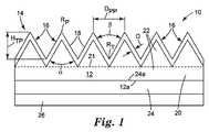
図1を参照すると、例示的な透明反射防止構造化フィルム10は、例えば光の反射を防止する角柱状リブレット16(図5を参照)の形態の反射防止構造体を含む主構造化面14を有する構造化フィルム基材12を備える。各反射防止構造体(例えば、リブレット)16は、先端角度α、谷から山の高さHTP、及び露出された構造化表面18を有する。隣接する2つの反射防止構造(例えば、リブレット)16は、谷角度βと、山から山の距離DPPとをそれらの間に画定する。フィルム10は更に、そこから反射防止構造体16が延出するベース部分20を有する。ベース部分20は、図に示されるように構造体16の一体形成された部分としてもよく、あるいは破線21によって示されるような別の層としてもよい。それらの耐久性を向上させるために、丸みのある山RP及び丸みのある谷RTを有するリブレット16を提供することが望ましい可能性がある。Referring to FIG. 1, an exemplary transparent anti-reflective
構造化フィルム基材12は、架橋シリコーンエラストマー材を含む。シリコーンエラストマー材は、例えば、熱硬化若しくは縮合硬化され得る2部分シリコーンゴム(例えば、Momentive RTV615 Silicone)、又電子ビーム(e−ビーム)硬化され得るポリジメチルシロキサン(例えば、Morrisville,PAのGelestから入手可能なDMS−S51)など、又はこれらの組み合わせであってもよい。構造化表面を形成するのに使用できるシリコーン材の他の特定の例は、例えばDow Corningから入手可能なSylgard 184、又はWacker Chemie AGから入手可能なElastosil 601)などの他のヒドロシリル化硬化シリコーン、例えばDow Corningから入手可能な732及び734 RTVシリコーンなどの縮合硬化シリコーン、並びに例えば、Gelestから入手可能なDMS−S42、又はWackerから入手可能なEL Polymer NAなどの電子ビーム架橋性シリコーンである。 The structured
構造化面14は、各構造体16の表面18の全部、又は殆ど、又は少なくとも実質的な部分を画定する架橋シリコーンエラストマー材を、化学量論的量のSiO2を含むガラス状材料に変換する処理に暴露される。そのような処理には、例えば、シリコーン材を真空紫外線(VUV)光(例えば、172nmエキシマVUVランプ処理)、真空紫外線光及びオゾン(VUVO)、火炎、酸素プラズマのうちの1つ又はこれらの組み合わせに暴露すること、並びに、化学量論的量のSiO2を有するように、シリコーンエラストマー材中のケイ素原子を転換することができる任意の他の処理を挙げることができる。このガラス状材料は、各構造体16内に深さDまで形成される。ガラス状材料の深さDは、暴露強度及び/又は処理の継続時間に依存する。それ故、ガラス状材料は、それぞれの構造体16内に架橋シリコーンエラストマー材のコア若しくは残りの部分22を残し、又は各構造16をガラス状材料で完全に形成されている状態とする深さDまで形成されてもよい。後者の実施形態では、未処理シリコーンエラストマー材から形成されているフィルム基材12の残りの部分(例えば、破線21の下方)が存在し得る。構造化表面18を形成する材料が化学量論的量のSiO2を示すにつれて、表面18は、汚れ及び埃粒子吸着(汚れ吸着試験結果で示される)、又は磨耗耐性(砂落下試験結果で示される)、又は両方に対して耐性となる可能性が高くなる。The structured
理論に束縛されるものではないが、ガラス状表面は、高エネルギー光子の吸収又は熱酸化による、反射防止構造体の露出表面上の又は該表面の付近のSi−C結合の破壊により形成されると考えられる。そのようなSi−C結合の破壊後、SiOHが生成され、これは縮合して化学量論的量のSiO2を形成する。Without being bound by theory, the glassy surface is formed by the breakage of Si-C bonds on or near the exposed surface of the antireflective structure by absorption or thermal oxidation of high energy photons. it is conceivable that. After the destruction of such Si-C bond, SiOH is generated, which forms SiO2 fused to the stoichiometric amount.
フィルム10又は本発明による任意の他の透明反射防止構造化フィルムは、場合により用いられる透明支持裏材24と組み合わせて使用することが望ましい場合がある。こうした実施形態では、支持裏材24は主面24aを有し、構造化フィルム基材12は更に支持裏材24の主面24aと結合される主裏打ち面12aを含むことにより、強化された透明反射防止構造化フィルムが形成される。支持裏材24は、高分子材料若しくはガラス、又は他の透明セラミック材料で形成することができる。例示的な高分子材料には、ポリメチル(メタ)アクリレート(PMMA)フィルム、ポリフッ化ビニリデン(PVDF)フィルム、ポリエチレンテレフタレート(PET)フィルム、プライミングされたPETフィルム、ポリカーボネートフィルム、架橋ポリウレタンフィルム、アクリレートフィルム、エチレンテ谷ルオロエチレン(ETFE)、フッ素化エチレン−プロピレン(FEP)フィルム、又はこれらのブレンドのうちの少なくとも1つ又は組み合わせが含まれる。紫外線光の吸収剤(例えば、Ciba Geigy製のTinuvin 1577、並びに両方がSukano Polymers Corporation,Duncan,SCから入手可能なSukano TA11−10 MB03 PMMA−UVA及びSukano TA07−07 MV02 PET−UVAなど)を、PMMA及びPVDFとPMMAとのブレンドに組み込んで、屋外耐久性を向上させることができる。他の透明セラミック材料は、例えば石英結晶などであってもよい。透明の不織布若しくは織布繊維材料、又は細断された透明繊維も、支持裏材24の形成に使用することができる。こうした繊維材料は、構造化フィルム10を形成するシリコーンエラストマー材中に配置され、又は構造化フィルム10上に配置され、又はその両方であってもよい。 It may be desirable to use
透明支持裏材24は、静電気を消散させるように選択することもできる。例えば、支持裏材は、支持裏材24に静電気を消散させるような1種以上の高分子材料を含むことができる。静電気を消散させるために、透明支持裏材24は、Lubrizol Corp.製のSTATRITE X5091ポリウレタン又はSTATRITE M809ポリメチルメタクリレートとして入手可能なものなどの、本質的に静電気消散性を有するポリマーも含み得る。代替的に、3M Companyから入手可能なFC4400などの静電気拡散性塩を、透明支持裏材24(例えば、PVDF)の作製に使用されるポリマーにブレンドしてもよい。加えて又は代替的に、構造化フィルム基材12はこうした静電気消散性塩を含んでもよい。 The transparent support backing 24 can also be selected to dissipate static electricity. For example, the support backing can include one or more polymeric materials that cause the support backing 24 to dissipate static electricity. In order to dissipate static electricity, the
支持裏材24に加えて又は支持裏材24の代わりに、フィルム10又は本発明による任意の他の透明反射防止構造化フィルムは、場合により用いられる水分バリア層26と組み合わせて使用することが望ましい場合もある。こうした実施形態では、耐水分バリア層26は、例えば水分バリア層26を1つ以上の中間層(例えば、支持裏材層24)を介して間接的に、又は構造化フィルム基材12の主裏打ち面12a上に直接的に積層し、又はコーティングし、又は結合することによって形成することができる。あるいは、水分バリア層26は、フィルム10の組成を水分バリア性を示すように(例えば、水分の吸収、浸透を阻止するように)配合することによって形成することもできる。 In addition to or instead of support backing 24,
水分バリアは、例えば、その全容が参照により本明細書に組み込まれる国際特許出願第PCT/US2009/062944号、米国特許第7,486,019号及び同第7,215,473号、並びに米国特許出願公開第2006/0062937 A1号に開示されているバリアアセンブリ、又は1つ以上のバリア層であってもよい。水分バリアは、シリコーンが高い湿気透過速度を有し、光電池が一般に水分感受性であるため有用であり得る。したがって、本発明の透明反射防止構造化フィルムは、水分バリア層により裏打ちされることによって、水分感受性の光電池(例えば、銅/インジウム/ガリウム/セレン又はCIGS光電池)上に直接使用することができる。 Moisture barriers are, for example, international patent applications PCT / US2009 / 062944, US Pat. Nos. 7,486,019 and 7,215,473, which are incorporated herein by reference in their entirety, and US Pat. It may be the barrier assembly disclosed in published application 2006/0062937 A1, or one or more barrier layers. A moisture barrier can be useful because silicone has a high moisture transmission rate and photovoltaic cells are generally moisture sensitive. Thus, the transparent antireflective structured film of the present invention can be used directly on moisture sensitive photovoltaic cells (eg, copper / indium / gallium / selenium or CIGS photovoltaic cells) by being lined with a moisture barrier layer.
図2を参照すると、本発明の透明反射防止構造化フィルムの別の実施形態10aでは、主構造化面14は、それぞれの反射防止構造体16の全部のシリコーンエラストマー材が、化学量論的量のSiO2を含むガラス状材料に変換される程度に/処理継続時間にて露出される。この実施形態では、フィルム基材12の残りの部分22はシリコーンエラストマー材のまま留まる。破線23は、基材12のガラス状材料部分をシリコーンエラストマー材部分から分離する。Referring to FIG. 2, in another
図3を参照すると、本発明の透明反射防止構造化フィルムの更なる実施形態10bでは、反射防止構造体16のそれぞれが別体のベース部分20’から延出している。別体のベース部分20’は架橋シリコーンエラストマー材の1つ以上の層であってもよく、あるいは別体のベース部分20’は異なる材料の1つ以上の層であってもよい(例えば、PMMA、PVDF及びPETなどのより安価な材料)。別体のベース部分20’は、シリコーンエラストマー材と異なる材料との適合性に応じて、任意の適当な手段によって反射防止構造体16に接着又は結合される。例えば、ベース部分20’は、シリコーンエラストマー反射防止構造体16のそれぞれの主裏打ち面16aを受承して、主裏打ち面16aと結合されるように場合に応じてプライマーでコーティングされるか、又は処理(例えば、コロナ放電処理)若しくは準備される主面20aを有し得る。反射防止構造体16は、例えば、その主面の少なくとも一方に反射防止構造体16の所望のパターンと一致する微小複製パターンが形成された金型フィルム(図に示されていない)によって形成することができる。 Referring to FIG. 3, in a
所望のシリコーンエラストマー前駆材料の層を、ベース部分面20aの表面上に押出し、又はコーティングし、又は適用することができる。次いで金型フィルムの微小複製された主面を、シリコーンエラストマー前駆材料の層と接触させることによって、適用されたシリコーンエラストマー前駆材料の露出表面を所望の反射防止構造体16の形状に形成することができる。代替的に、シリコーンエラストマー前駆材料の層を金型フィルムの微小複製された主面上に押出し、又はコーティングし、又は適用し、次いで適用された前駆材料の露出した裏面をベース部分面20aの表面と積層し又は接触させて結合させてもよい。代替的に、全ての3つの層は、例えばニップロールステーションに通過させることにより一緒に積層されるときに、シリコーンエラストマー前駆材料の層を、金型フィルムの微小複製された主面とベース部分面20aの表面との間に直接的に押出し、又はコーティングし、又は別様に適用してもよい。形成された前駆材料をベース部分面20aの表面と接触させた時点で、最初にシリコーンエラストマー前駆材料を架橋又は硬化させ、金型を取り除き、この後、反射防止構造体16の少なくとも表面18にガラス状の材料を生じさせる処理を行う。 A layer of the desired silicone elastomer precursor material can be extruded, coated, or applied onto the surface of the
反射防止構造体は、角柱状、角錐状、円錐状、半球状、放物線状、円筒状、及び柱状構造体の少なくとも1つ又は組み合わせで構成され得る。角柱を含む反射防止構造体は、約90°未満、約60°以下、約30°以下、又は約10°〜約90°までの範囲内の角柱先端角度αを有し得る。そのような反射防止角柱構造体は、約2マイクロメートル〜約2cmの範囲内の谷から谷の、又は山から山のピッチ又は距離も有し得る。角柱を含む反射防止構造体は、約15度〜約75度の範囲内の角柱先端角度も有し得る。角柱を含む反射防止構造体は、約10マイクロメートル〜約250マイクロメートルの範囲内の谷から谷の、又は山から山のピッチも有し得る。向上された耐久性を有する反射防止構造体16の一実施形態では、リブレット16は、丸みのある山RP及び谷RTを有し、約5マイクロメートルの半径、約53度の谷角度β、約50マイクロメートルの山から山のピッチ又は距離DPP、並びに約37.7307マイクロメートルの谷から山の高さHTPを有する。The antireflection structure may be composed of at least one or a combination of prismatic, pyramidal, conical, hemispherical, parabolic, cylindrical, and columnar structures. An antireflective structure that includes a prism may have a prism tip angle α less than about 90 °, less than about 60 °, less than about 30 °, or in a range from about 10 ° to about 90 °. Such anti-reflective prismatic structures may also have valley-to-valley or peak-to-peak pitches or distances in the range of about 2 micrometers to about 2 cm. An antireflective structure that includes a prism may also have a prism tip angle within a range of about 15 degrees to about 75 degrees. An anti-reflective structure that includes a prism may also have a valley-to-valley or peak-to-peak pitch within the range of about 10 micrometers to about 250 micrometers. In one embodiment of the
反射防止構造体は、約1.55未満の屈折率、好ましくは約1.50未満の屈折率を示すことが望ましい場合がある。反射防止構造体が角柱構造体を有する場合(例えば、直線状角柱構造体又はリブレット)、それぞれの角柱が、それらの基部から約90°未満の頂角、好ましくは約60°以下の頂角を有する先端へと幅が狭くなることが望ましい場合がある。このような角柱構造体は、約10マイクロメートル〜約250マイクロメートルの範囲内の、谷から山の高さを有することが望ましい場合がある。このような角柱構造体は、約25マイクロメートル〜約100マイクロメートルの範囲内の、谷から山の高さを有することが望ましい場合もある。 It may be desirable for the antireflective structure to exhibit a refractive index less than about 1.55, preferably less than about 1.50. When the antireflective structure has a prismatic structure (eg, a linear prismatic structure or riblet), each prism has an apex angle of less than about 90 °, preferably no more than about 60 ° from their base. It may be desirable for the width to narrow towards the tip it has. It may be desirable for such prismatic structures to have valley to mountain heights in the range of about 10 micrometers to about 250 micrometers. It may be desirable for such prismatic structures to have valley-to-mountain heights in the range of about 25 micrometers to about 100 micrometers.
本発明の透明反射防止構造化フィルムは、構造化表面を汚れ吸着試験、又は砂落下試験、又は両試験の組み合わせに曝露した後に、少なくとも約85%、90%、91%、92%、93%、94%、95%、96%、97%、98%又は99%の光透過率を示すことが望ましい場合がある。これらの試験については後述する。本発明の透明反射防止構造化フィルムは、構造化表面を汚れ吸着試験、又は砂落下試験、又は両試験の組み合わせに曝露した後に、10%、9%、8%、7%、6%、5%、4%、3%、2%又は1%未満の光透過率の変化を示すことが望ましい場合もある。 The transparent antireflective structured film of the present invention has at least about 85%, 90%, 91%, 92%, 93% after exposing the structured surface to a soil adsorption test, or a sand drop test, or a combination of both tests. , 94%, 95%, 96%, 97%, 98% or 99% light transmission may be desirable. These tests will be described later. The transparent antireflective structured film of the present invention is 10%, 9%, 8%, 7%, 6%, 5% after exposing the structured surface to a dirt adsorption test, or a sand drop test, or a combination of both tests. It may be desirable to exhibit a change in light transmission of less than 4%, 4%, 3%, 2% or 1%.
本発明の透明反射防止構造化フィルムは、反射防止構造体のシリコーンエラストマー材中に無機粒子、好ましくはナノ粒子を含んでもよい。これらの粒子には、任意の好適な無機材料が含まれ得る(例えば、シリカ、ジルコニア、チタニアなど、又はこれらの任意の組み合わせ)。そのような粒子はまた、シラン表面改質剤で被覆されてシリコーン中での分散を促進してもよい。こうした粒子は、約2.0マイクロメートル以下の範囲内の粒径を有するものでよい。シリカ粒子は最大でマイクロメートルサイズであってよいが、他の材料で形成された粒子はナノメートルサイズのものが使用されることが好ましい(即ち、約5nm〜約50nm以下の範囲内)。こうした粒子、特にナノ粒子は、0重量%〜約60重量%以下の範囲内でシリコーンエラストマー材中に添加してもよい。 The transparent antireflection structured film of the present invention may contain inorganic particles, preferably nanoparticles, in the silicone elastomer material of the antireflection structure. These particles can include any suitable inorganic material (eg, silica, zirconia, titania, etc., or any combination thereof). Such particles may also be coated with a silane surface modifier to promote dispersion in the silicone. Such particles may have a particle size in the range of about 2.0 micrometers or less. Silica particles can be up to micrometer size, but particles made of other materials are preferably nanometer sized (ie, in the range of about 5 nm to about 50 nm or less). Such particles, particularly nanoparticles, may be added to the silicone elastomer material in the range of 0 wt% to about 60 wt% or less.
図4を参照すると、本発明の透明反射防止構造化フィルム10のいずれの実施形態も、例えば、光源熱エネルギー吸収装置(例えば、太陽光温水システム)、光起電装置、又は任意の他の光エネルギー吸収装置などの光エネルギー吸収装置30において使用することができる。こうした装置30は、光エネルギー受容面32aを有する光吸収器32(例えば、光電池)を更に含み、透明反射防止構造化フィルム10が、光エネルギーの供給源(例えば、太陽)と光エネルギー受容面32aとの間となるように光吸収器32に対して配置される。これにより、光源からの光エネルギーは、光吸収器32によって吸収される前に構造化フィルム10を通過することになる。フィルム10は、光エネルギー受容面32aに結合、接着、機械的に締結又は直接接触させて配置することができる。また、必要な場合には、1つ以上の透明支持裏材24又は他の中間層を、フィルム10と光吸収器32との間に配置することができる。 Referring to FIG. 4, any embodiment of the transparent anti-reflective
図5を参照すると、本発明の透明反射防止構造化フィルム10を光エネルギー吸収装置30の光吸収器32とともに使用することにより、反射防止構造体16の表面18に入射する入射光(矢印40により示される)が複数回反射される可能性が高くなる(矢印40Rにより示される)。このような光40の複数回の反射によって、光40が光吸収器32内へと屈折する確率、及び入射光の受容角が大きくなる確率が高くなる。このように、こうした透明反射防止構造体の使用により、装置30の効率及びエネルギー出力を高めることが可能である。Referring to FIG. 5, by using the transparent antireflection structured
光エネルギー吸収装置が光起電装置の場合、光吸収器は、太陽光又は他の光エネルギーを電気エネルギーに変換するための少なくとも1つの光電池を有する光電池モジュールである。反射防止構造化フィルムは表面反射を低減し、これは光電池上に衝突する光の量を増大させ、電気エネルギー生成の増大をもたらすことができる。このようにして本発明の透明反射防止構造化フィルムを使用することにより、光エネルギーを電気エネルギーに変換する効率を、少なくとも約3%、場合により約5%〜約10%以下の範囲内で高めることが可能である。透明反射防止構造体はフィルムの形態であるため、光電池は、破損することなくロールに巻いたり、折り畳めたりするような充分な可撓性及び柔軟性を有し得る。 When the light energy absorber is a photovoltaic device, the light absorber is a photovoltaic module having at least one photovoltaic cell for converting sunlight or other light energy into electrical energy. Anti-reflective structured films reduce surface reflections, which can increase the amount of light impinging on the photovoltaic cells, resulting in increased electrical energy generation. Thus, by using the transparent antireflective structured film of the present invention, the efficiency of converting light energy into electrical energy is increased by at least about 3%, and in some cases from about 5% to about 10% or less. It is possible. Since the transparent antireflective structure is in the form of a film, the photovoltaic cell can have sufficient flexibility and flexibility to wind or fold on a roll without breakage.
本発明の光エネルギー吸収装置は、反射防止構造化フィルムを通って光吸収器(例えば、光電池)の光受容面へと光が通過できるように、光吸収器に反射防止構造化フィルムを機械的に取り付け、又は接着剤により接着し、又は他の手段により固定することによって作製することができる。光吸収器は例えば、太陽光温水ヒーター又は他の光により発生する熱エネルギーの吸収装置、太陽光エネルギー又は他の光エネルギーを電気エネルギーに変換するための光電池、又はこれらの組み合わせであってよい。 The light energy absorber of the present invention mechanically attaches an antireflection structured film to the light absorber so that light can pass through the antireflection structured film to the light receiving surface of the light absorber (eg, photovoltaic cell). It can be made by attaching to, or adhering with an adhesive, or fixing by other means. The light absorber may be, for example, a solar water heater or other light energy absorbing device generated by light, a photovoltaic cell for converting solar energy or other light energy into electrical energy, or a combination thereof.
本発明による透明反射防止構造化フィルムは、上述したような透明構造化フィルム基材を提供した後、構造化表面を画定する架橋シリコーンエラストマー材の全部、又は殆ど、又は少なくとも実質的な部分が、化学量論的量のSiO2を含むガラス状材料に変換されるように、構造化表面を処理することにより作製することができる。初期の構造化フィルム基材の反射防止構造化表面を、例えば該表面を真空紫外線(VUV)光(例えば、172nmエキシマ処理により)、真空紫外線光及びオゾン(VUVO)、酸素プラズマ、並びに熱(例えば、誘導加熱、火炎など)のうちの少なくとも1つ又は組み合わせなどの任意の好適な処理に暴露することにより処理して、ガラス状表面を形成してもよい。高真空製造の設定での使用に好適であるように、そのような処理は、比較的急速に行われる必要がある。特に、例えば高速(即ち、大量)ウェブベース製造プロセスでは、例えば約5分以下の短い処理時間を用いる必要があるであろう。同時に、シリコーン材の表面は、十分な期間(例えば、5〜300秒間の172nmエキシマランプ暴露)、かつ好適なエネルギーレベル(例えば、酸素50ppm未満の窒素不活性雰囲気中で10〜50mW/cm2)で処理されて、ケイ素から化学量論的量のSiO2への所望のレベルの転換を生じる必要がある。ガラス状表面の生成に用いられる処理の設定(例えば、強度及び/又は継続時間)に応じて、ガラス状材料に転換されていない構造化フィルム基材の残りの部分が存在し得る。例えば図2から明らかなように、処理設定はまた、反射防止構造体のそれぞれを画定する架橋シリコーンエラストマー材の全部が、化学量論的量のSiO2を含むガラス状表面に変換されるように選択されてもよい。代替的に、処理設定は、反射防止構造体のそれぞれのコア部分がシリコーンエラストマー材のまま留まるように選択されてもよい(図1、3及び4参照)。エネルギー費用を節約するために、反射防止構造化表面がガラス状表面に転換される深さ及び程度を最小限にすることが望ましい場合がある。The transparent antireflective structured film according to the present invention provides a transparent structured film substrate as described above, after which all or most or at least a substantial portion of the crosslinked silicone elastomer material defining the structured surface is It can be made by treating the structured surface so that it is converted to a glassy material containing a stoichiometric amount of SiO2 . An anti-reflective structured surface of an initial structured film substrate, such as vacuum ultraviolet (VUV) light (eg, by 172 nm excimer treatment), vacuum ultraviolet light and ozone (VUVO), oxygen plasma, and heat (eg, Treatment by exposure to any suitable treatment such as at least one or a combination of induction heating, flame, etc.) to form a glassy surface. In order to be suitable for use in a high vacuum manufacturing setting, such processing needs to be performed relatively quickly. In particular, for example, high speed (ie, high volume) web-based manufacturing processes may require the use of short processing times, for example about 5 minutes or less. At the same time, the surface of the silicone material has a sufficient duration (eg, exposure to a 172 nm excimer lamp for 5 to 300 seconds) and a suitable energy level (eg, 10-50 mW / cm2 in a nitrogen inert atmosphere with less than 50 ppm oxygen). To produce the desired level of conversion from silicon to stoichiometric amounts of SiO2 . Depending on the treatment settings (eg, strength and / or duration) used to generate the glassy surface, there may be a remaining portion of the structured film substrate that has not been converted to a glassy material. As can be seen, for example, from FIG. 2, the treatment setting also ensures that all of the crosslinked silicone elastomer material defining each of the antireflective structures is converted to a glassy surface containing a stoichiometric amount of SiO2. It may be selected. Alternatively, the processing settings may be selected such that each core portion of the antireflective structure remains a silicone elastomer material (see FIGS. 1, 3 and 4). In order to save energy costs, it may be desirable to minimize the depth and extent to which the antireflective structured surface is converted to a glassy surface.
透明構造化フィルム基材は、硬化性であることで架橋シリコーンエラストマー材料を形成するシリコーンエラストマー前駆材料を与えることによって作製することができる。このシリコーンエラストマー前駆材料は、任意の適当な形成方法によって構造化フィルム基材の形状に形成される。例えば、適当な大きさの溝を基材に形成した後、この基材を鋳型表面として使用してその上にシリコーンエラストマー前駆材料をコーティングすることによって、構造化フィルム基材の反射防止構造体を有する主構造化面を成形することができる。このような鋳型基材は、例えば、その全容が参照により本明細書に組み込まれる米国特許出願公開第2006/0234605号に開示される方法及び装置に基づいて作製することができる。シリコーンエラストマー前駆材料は、この形状で硬化させることで構造化フィルム基材が形成される。代替的に、米国特許出願第2006/0234605号に開示される金型を使用して、適当な大きさの溝を高分子鋳型基材(例えば、フィルムの形態の)に成形した後、これを鋳型表面として使用することもできる。使用するシリコーンシリコーンエラストマー前駆材料に応じて、硬化プロセスにおいて前駆材料に架橋処理を行ってもよい(例えば、熱及び/又は放射線処理)。前駆材料が2成分型の自己硬化型シリコーンエラストマー材である場合、硬化プロセスにおいて、2成分を混合した後、前駆材料を鋳型表面と充分に長い時間、接触状態に維持することで架橋を生じさせることができる。 Transparent structured film substrates can be made by providing a silicone elastomer precursor that is curable to form a crosslinked silicone elastomer material. The silicone elastomer precursor material is formed into the shape of a structured film substrate by any suitable forming method. For example, an antireflective structure for a structured film substrate can be obtained by forming a suitably sized groove in a substrate and then coating the silicone elastomer precursor on it using the substrate as a mold surface. The main structured surface can be molded. Such a mold substrate can be made, for example, based on the method and apparatus disclosed in US Patent Application Publication No. 2006/0234605, the entirety of which is incorporated herein by reference. The silicone elastomer precursor is cured in this shape to form a structured film substrate. Alternatively, the mold disclosed in US Patent Application No. 2006/0234605 may be used to form a suitably sized groove into a polymeric mold substrate (eg, in the form of a film) and then It can also be used as a mold surface. Depending on the silicone silicone elastomer precursor material used, the precursor material may be subjected to a crosslinking treatment in the curing process (eg, heat and / or radiation treatment). If the precursor material is a two-component self-curing silicone elastomer material, after the two components are mixed in the curing process, the precursor material is kept in contact with the mold surface for a sufficiently long time to cause crosslinking. be able to.
以下の実施例は、単に本発明の特徴、利点、及び/又は他の細部を更に説明するために選択したものである。しかしながら、実施例はこの目的を果たすものではあるが、使用される特定の成分及びその量、並びに他の条件及び詳細は、本発明の範囲を必要以上に限定するものとして解釈されるべきではない点は明確に理解されるはずである。 The following examples have been selected merely to further illustrate features, advantages, and / or other details of the invention. However, while the examples serve this purpose, the particular components used and their amounts, as well as other conditions and details, should not be construed as unduly limiting the scope of the invention. The point should be clearly understood.
実施例1
Waterford,New YorkのMomentive Performance Materialsから入手可能なRTV615のA液及びRTV615のB液を10:1の比で混合し、4枚の石英スライドガラスのそれぞれに厚さ100マイクロメートルでコーティングした。次いで、シリコーンコーティングされた石英スライドガラスを対流式オーブン中で85℃に30分加熱し、熱硬化性シリコーンエラストマーの前駆材料を架橋/硬化させた。次いで、これらの架橋シリコーンでコーティングされたスライドガラス(サンプル2〜5)を、表1に示す火炎処理に暴露した。次いで、これらの火炎処理したシリコーンコーティングガラス構造を、ナノインデンテーションにより貯蔵弾性率に関して分析した。これらの火炎処理シリコーンコーティングガラス構造における弾性率変化を、表1に示す。Example 1
RTV615 solution A and RTV615 solution B, available from Momentive Performance Materials of Waterford, New York, were mixed at a ratio of 10: 1 and coated on each of the four quartz slides at a thickness of 100 micrometers. The silicone coated quartz glass slide was then heated to 85 ° C. for 30 minutes in a convection oven to crosslink / cure the thermoset silicone elastomer precursor. The glass slides (Samples 2-5) coated with these crosslinked silicones were then exposed to the flame treatment shown in Table 1. These flame treated silicone coated glass structures were then analyzed for storage modulus by nanoindentation. Table 1 shows the change in elastic modulus in these flame-treated silicone-coated glass structures.

実施例2
14枚の7.6cm(3インチ)×5.1cm(2インチ)のスライドガラス(VWR International,LLC.から入手可能)をナノシリカベースのプライマーで下塗りした。このナノシリカプライマーは、HNO3で2.5〜2.0のpHにした、第一コロイドシリカ(「NALCO 1115 COLLOIDAL SILICA」)と第二コロイドシリカ(「NALCO 1050 colloidal SILICA」)の重量比70:30ブレンドの5重量% H2O溶液から構成される。このナノシリカプライマー溶液で湿らせた小さな拭取り布(Kimberly−Clark,Roswell,GAから商品名「KIMTECH」で入手)で表面を拭くことにより、プライマーの薄い(約100ナノメートル)均質コーティングを各スライドガラスに適用した。プライマーを室温で乾燥させた。添加硬化シリコーン(Sylgard 184,Dow Corning,Midland,MIから入手可能)を10:1(A液対B液)の比で混合し、下塗りしたスライドスライドガラスに平滑コーティング(smooth coating)にて厚さ45マイクロメートルで適用し、48時間かけて完全に硬化させた。サンプル6及び7の場合、シリコーン表面を処理しなかった一方、サンプル8〜19は、27インチ(38.58cm)下方駆動電極及び中央ガスポンプとともに反応性イオンエッチング(RIE)用に構成された市販のバッチプラズマシステム(Plasmathermモデル3032)を使用して、酸素プラズマ処理した。このチャンバを、ドライメカニカルポンプ(EdwardsモデルiQDP80)によりバックアップされたルーツブロワー(EdwardsモデルEH1200)により排気する。3kWの13.56Mhzソリッドステート発生器(RFPPモデルRF30H)によりRF電力をインピーダンスマッチングネットワークから送達する。このシステムは、5mTorr(0.67Pa)の公称のベース圧力を有する。ガスの流量をMKSフローコントローラーにより制御する。プラズマ処理用の基材を、下方駆動電極上に配置する。シリコーンコーティングスライドガラスを、バッチプラズマ機器の駆動電極上に配置した。酸素プラズマを用いて、酸素ガス(Oxygen Service Corporation,UHP等級)を流量500標準cm3/分で流し、3000ワットのプラズマ出力で90秒間、プラズマ処理を行った。プラズマ処理が完了した後、チャンバを大気中に通気し、サンプルを取り出した。Example 2
Fourteen 7.6 cm (3 inches) by 5.1 cm (2 inches) glass slides (available from VWR International, LLC.) Were primed with a nanosilica-based primer. This nanosilica primer was made with HNO3 to a pH of 2.5-2.0, a weight ratio of first colloidal silica (“NALCO 1115 COLLOIDAL SILICA”) to second colloidal silica (“NALCO 1050 colloidal SILICA”) 70: 30 consists of 5 wt%H 2 O solution of the blend. A thin (approx. 100 nanometers) homogeneous coating of primer on each slide by wiping the surface with a small wipe dampened with this nanosilica primer solution (obtained under the trade designation “KIMTECH” from Kimberly-Clark, Roswell, GA) Applied to glass. The primer was dried at room temperature. Addition-cured silicone (available from Sylgard 184, Dow Corning, Midland, MI) is mixed at a ratio of 10: 1 (solution A to solution B) and thickened with a smooth coating on the primed slide glass slide. Applied at 45 micrometers and allowed to fully cure over 48 hours. In the case of Samples 6 and 7, the silicone surface was not treated, while Samples 8-19 were commercially available for reactive ion etching (RIE) configured with a 27 inch (38.58 cm) lower drive electrode and a central gas pump. Oxygen plasma treatment was performed using a batch plasma system (Plasmatherm model 3032). The chamber is evacuated by a roots blower (Edwards model EH1200) backed up by a dry mechanical pump (Edwards model iQDP80). RF power is delivered from the impedance matching network by a 3 kW 13.56 Mhz solid state generator (RFPP model RF30H). This system has a nominal base pressure of 5 mTorr (0.67 Pa). The gas flow rate is controlled by the MKS flow controller. A substrate for plasma treatment is disposed on the lower drive electrode. A silicone coated glass slide was placed on the drive electrode of the batch plasma instrument. Using oxygen plasma, oxygen gas (Oxygen Service Corporation, UHP grade) was flowed at a flow rate of 500 standard cm 3 / min, and plasma treatment was performed for 90 seconds at a plasma output of 3000 watts. After the plasma treatment was completed, the chamber was vented to the atmosphere and the sample was removed.
サンプル6〜17を、1枚のコーティングしていないそのままのスライドガラスとともに、以下に述べる汚れ吸着試験#1に一定期間ごとに供した。試験を行う前の最初の光透過率を(Ti)、試験を行った後の最終的な光透過率を(Tf)とし、最初の光透過率と最終的な光透過率との差(Td)を下記表2(汚れ吸着試験#1結果)にそれぞれについて示した。透過率計を使用して、透過率を試験した。表のデータは、未処理サンプル6及び7と比較して、酸素プラズマ処理サンプル8〜17の光透過率が有意に増大していることを示す。この光透過率における相違は、更に処理されたシリコーンエラストマー表面(サンプル8〜17)が、未処理サンプル6及び7と比較して、汚れの吸着及び保持量が少ないことによる。表2のデータは、処理サンプル6〜17が、そのままのスライドガラスの光透過率と同等の光透過率を有したことも示す。 Samples 6 to 17 were subjected to a soil adsorption test # 1 described below together with a single uncoated glass slide at regular intervals. The initial light transmittance before the test is (Ti), the final light transmittance after the test is (Tf), and the difference between the initial light transmittance and the final light transmittance (Td) ) Is shown in Table 2 below (results of dirt adsorption test # 1). The transmission was tested using a transmission meter. The data in the table shows that the light transmission of oxygen plasma treated samples 8-17 is significantly increased compared to untreated samples 6 and 7. This difference in light transmission is due to the fact that the further treated silicone elastomer surfaces (samples 8-17) have less dirt adsorption and retention compared to untreated samples 6 and 7. The data in Table 2 also shows that treated samples 6-17 had a light transmission equivalent to that of the glass slide as it was.
サンプル18及び19を、以下に述べる砂落下試験に供した。試験を行う前の最初の光透過率を(Ti)、試験を行った後の最終的な光透過率を(Tf)とし、最初の光透過率と最終的な光透過率との差(Td)を下記表3(砂落下試験)に示した。表のデータは、処理サンプル18〜19が、そのままのスライドガラスの光透過率と同等の光透過率を有したことを示す。
サンプル18及び19はまた、砂落下試験の直後に汚れ試験#に供され、初期透過率(Ti)は砂落下試験後の透過率値を表し、最終透過率(Tf)は汚れ試験後の透過率値を表し、初期透過率と最終透過率(Td)との差を下記表4(砂落下試験直後の汚れ試験#1結果)に示した。表のデータは、酸素プラズマ処理シリコーンサンプルが、そのままのスライドガラスの性能から2%の範囲内にあることを示す。
実施例3
2枚の30.5cm(12インチ)×15.2cm(6インチ)のポリエチレンテレフタレート(PET)シート(DuPont Teijin Films,Chester,VAから商品名「MELINEX 618」で入手)を、ナノシリカベースのプライマーで下塗りした。このナノシリカプライマーは、HNO3で2.5〜2.0のpHにした、第一コロイドシリカ(「NALCO 1115 COLLOIDAL SILICA」)と第二コロイドシリカ(「NALCO 1050 colloidal SILICA」)の重量比70:30ブレンドの5重量% H2O溶液から構成される。このナノシリカプライマー溶液で湿らせた小さな拭取り布(Kimberly−Clark(Roswell,GA)から商品名「KIMTECH」で入手)で表面を拭くことにより、プライマーの薄い(約100ナノメートル)均質コーティングを各スライドガラスに適用した。プライマーを室温で乾燥させた。シラノール末端ポリジメチルシロキサン流体(DMS−S51、Gelest Inc.,Morrisville,PAから入手可能)を、下塗りしたPETフィルム上に、ノッチバーコーターを使用して厚さ100マイクロメートルでコーティングした。シリコーンコーティングを有するPETフィルムを支持ウェブにテープで貼り、加速電圧190keV(3.044×10⁻¹⁴J)及び照射量10MRads(0.1mGy)で、電子ビームに通過させた。E−ビームユニットは、ブロードバンドカーテンタイプの電子ビームプロセッサ(PCT Engineered Systems,LLCから入手)であった。シリコーンコーティングフィルムの1つから6片(サンプル20、21、22、23、24及び25)を切り取り、サンプル20、21、22及び23は、窒素パージングを有する放射照度10mW/cm2での120秒の172nmエキシマランプ(モデルUER20−172、Ushio America,Inc.,Cypress,CAから入手可能)に暴露されたシリコーンコーティングの表面を有した。サンプル24及び25は、エキシマランプ処理を受けなかった。他のシリコーンコーティングフィルムから6片(サンプル26、27、28、29、30及び31)を切り取り、これらは120keV(1.923×10⁻¹⁴J)及び照射量15MRad/通過での4回の通過からなる追加のe−ビーム照射量を受けて、表面を更に架橋させた。次いで、サンプル26、27、28及び29を、172nmエキシマランプに、放射照度10mW/cm2で120秒間暴露した。サンプル30及び31は、エキシマランプ処理を受けなかった。Example 3
Two 30.5 cm (12 inches) by 15.2 cm (6 inches) polyethylene terephthalate (PET) sheets (obtained under the trade designation “MELINEX 618” from DuPont Teijin Films, Chester, Va.) With a nanosilica-based primer Primed. This nanosilica primer was made with HNO3 to a pH of 2.5-2.0, a weight ratio of first colloidal silica (“NALCO 1115 COLLOIDAL SILICA”) to second colloidal silica (“NALCO 1050 colloidal SILICA”) 70: 30 consists of 5 wt%H 2 O solution of the blend. Each thin (approx. 100 nanometer) homogeneous coating of primer was wiped with a small wiping cloth (obtained under the trade designation “KIMTECH” from Kimberly-Clark (Roswell, GA)) moistened with this nanosilica primer solution. Applied to slide glass. The primer was dried at room temperature. Silanol-terminated polydimethylsiloxane fluid (DMS-S51, available from Gelest Inc., Morrisville, Pa.) Was coated onto the primed PET film at a thickness of 100 micrometers using a notch bar coater. A PET film having a silicone coating was taped to a support web and passed through an electron beam with an acceleration voltage of 190 keV (3.044 × 10⁻¹⁴ J) and an irradiation dose of 10 MRads (0.1 mGy). The E-beam unit was a broadband curtain type electron beam processor (obtained from PCT Engineered Systems, LLC). Six pieces (
サンプル20、21、24、26、27及び30を、以下に述べる汚れ吸着試験#1に供した。試験を行う前の最初の光透過率を(Ti)、試験を行った後の最終的な光透過率を(Tf)とし、最初の光透過率と最終的な光透過率との差(Td)を下記表5(汚れ吸着試験#1結果)にそれぞれについて示した。表のデータは、未処理サンプル24及び30と比較して、更に処理された20、21、26及び27の光透過率が有意に増大していることを示す。この光透過率における相違は、更に処理されたシリコーンエラストマー表面(サンプル20、21、26及び27)が、未処理サンプル24及び30と比較して、汚れの吸着及び保持量が少ないことによる。表5のデータは、処理サンプル20、21、26及び27が、表5のそのままのスライドガラスの光透明度と同等の光透明度を有したことも示す。表は、サンプル30における追加の電子ビーム架橋が、172nmエキシマランプ処理を有さなくても、電子ビーム及び172nmエキシマランプ処理のいずれも受けなかったサンプル24と比較して、低い透過率損失をもたらすことも示す。
サンプル22、23、25、28、29及び31を、以下に述べる砂落下試験に供した。試験を行う前の最初の光透過率を(Ti)、試験を行った後の最終的な光透過率を(Tf)とし、最初の光透過率と最終的な光透過率との差(Td)を下記表6(砂落下試験)に示した。表のデータは、172nmエキシマランプ処理に先だって更に電子ビーム架橋されたサンプル28及び29は、更に電子ビーム架橋されなかったサンプル22及び23と比較して、光透過率(即ち、砂落下試験結果)が増大していることを示す。表は、サンプル31において、172nmエキシマランプ処理を有さなかった追加の電子ビーム橋架が、追加の電子ビーム橋架又は172nmエキシマランプ処理のいずれも受けなかったサンプル25、172nmエキシマランプ処理のみを受けたサンプル22及び23、追加の電子ビーム架橋及び172nmエキシマランプ処理の両方を受けたサンプル28及び29と比較して、低い透過率損失をもたらすことも示す。
実施例4
2枚の30.5cm(12インチ)×15.2cm(6インチ)のポリエチレンテレフタレート(PET)シート(DuPont Teijin Films,Chester,VAから商品名「MELINEX 618」で入手)を、ナノシリカベースのプライマーで下塗りした。このナノシリカプライマーは、HNO3で2.5〜2.0のpHにした、第一コロイドシリカ(「NALCO 1115 COLLOIDAL SILICA」)と第二コロイドシリカ(「NALCO 1050 colloidal SILICA」)の重量比70:30ブレンドの5重量% H2O溶液から構成される。このナノシリカプライマー溶液で湿らせた小さな拭取り布(Kimberly−Clark(Roswell,GA)から商品名「KIMTECH」で入手)で表面を拭くことにより、プライマーの薄い(約100ナノメートル)均質コーティングを各スライドガラスに適用した。プライマーを室温で乾燥させた。熱硬化シリコーンエラストマー(Sylgard 184、Dow Corning,Midland,MIから入手可能)を、裏打ちしたPETと、反射防止表面構造を含むポリプロピレン金型フィルムとの間にコーティングした。シリコーンコーティング及びポリプロピレン金型フィルムを有するPETフィルムを、75℃の炉内に90分間配置して、シリコーンコーティングを硬化させた。フィルムを炉から取り出した後、金型フィルムを除去し、PETフィルムに取り付けられた表面構造化反射防止シリコーンコーティングを得た。シリコーン表面構造体の表面の耐久性を向上させるために、次いでコーティングされたフィルムの1つのシートを支持ウェブにテープで貼り、加速電圧120keV(1.923×10⁻¹⁴J)及び15MRads/通過(0.15mGy/通過で電子ビームに4回通過させて、追加の架橋を提供した。E−ビームユニットは、ブロードバンドカーテンタイプの電子ビームプロセッサ(PCT Engineered Systems,LLCから入手)であった。Example 4
Two 30.5 cm (12 inches) by 15.2 cm (6 inches) polyethylene terephthalate (PET) sheets (obtained under the trade designation “MELINEX 618” from DuPont Teijin Films, Chester, Va.) With a nanosilica-based primer Primed. This nanosilica primer was made with HNO3 to a pH of 2.5-2.0, a weight ratio of first colloidal silica (“NALCO 1115 COLLOIDAL SILICA”) to second colloidal silica (“NALCO 1050 colloidal SILICA”) 70: 30 consists of 5 wt%H 2 O solution of the blend. Each thin (approx. 100 nanometer) homogeneous coating of primer was wiped with a small wiping cloth (obtained under the trade designation “KIMTECH” from Kimberly-Clark (Roswell, GA)) moistened with this nanosilica primer solution. Applied to slide glass. The primer was dried at room temperature. A thermoset silicone elastomer (available from Sylgard 184, Dow Corning, Midland, MI) was coated between the lined PET and a polypropylene mold film containing an antireflective surface structure. A PET film with a silicone coating and a polypropylene mold film was placed in an oven at 75 ° C. for 90 minutes to cure the silicone coating. After removing the film from the furnace, the mold film was removed to obtain a surface structured anti-reflective silicone coating attached to the PET film. To improve the durability of the surface of the silicone surface structure, one sheet of the coated film was then taped to the support web, with an acceleration voltage of 120 keV (1.923 × 10⁻¹⁴ J) and 15 MRads / pass ( The electron beam was passed four times at 0.15 mGy / pass to provide additional cross-linking The E-beam unit was a broadband curtain type electron beam processor (available from PCT Engineered Systems, LLC).
追加の電子ビーム処理を受けなかったシリコーンコーティングフィルムのうちの1つから4片(サンプル32、33、34及び35)を切り取り、サンプル32及び33は、窒素パージングを有する放射照度およそ10mW/cm2での172nmエキシマランプ(モデルUER20−172 Ushioから販売)に300秒間暴露されたシリコーンコーティングの表面を有した。サンプル34及び35は、エキシマランプ処理を受けなかった。追加のe−ビーム処理を受けた他のシリコーンコーティングフィルムから、4片(サンプル36、37、38及び39)を切り取った。次いで、サンプル37及び37を、172nmエキシマランプに、放射照度およそ10mW/cm2で300秒間暴露した。サンプル38及び39は、エキシマランプ処理を受けなかった。Four pieces (
サンプル32、34、36及び38を、以下に述べる汚れ吸着試験#1に供した。試験を行う前の最初の光透過率を(Ti)、試験を行った後の最終的な光透過率を(Tf)とし、最初の光透過率と最終的な光透過率との差(Td)を下記表7(汚れ吸着試験#1結果)にそれぞれについて示した。表のデータは、未処理サンプル34及び38と比較して、172nmエキシマランプ処理されたサンプル32及び36の光透過率が有意に増大していることを示す。この光透過率の相違は、172nmエキシマランプ処理されたシリコーンエラストマーの表面(サンプル32及び36)が、未処理サンプル34及び38と比較して、汚れの吸着及び保持量が少ないことによる。表7のデータは、172nmエキシマランプ処理に先だって更なる電子ビーム橋架を受けたサンプル36が、172nmエキシマランプ処理のみを受けたサンプル32と比較して、より良好な汚れ吸着試験結果を生じることも示す。
サンプル33、35、37及び39を、以下に述べる砂落下試験に供した。試験を行う前の最初の光透過率を(Ti)、試験を行った後の最終的な光透過率を(Tf)とし、最初の光透過率と最終的な光透過率との差(Td)を下記表8(砂落下試験)に示した。表のデータは、172nmエキシマランプで処理されなかったサンプル35及び39と比較して、172nmエキシマランプ処理を受けたサンプル33及び37の光透過率(即ち、砂落下試験結果)が増大していることを示す。更に電子ビーム架橋されなかったサンプル33及び35と比較して、172nmエキシマランプ処理に先だって更に電子ビーム架橋されたサンプル37及び39の光透過率(即ち、砂落下試験結果)が増大していることも理解される。 Samples 33, 35, 37 and 39 were subjected to the sand drop test described below. The initial light transmittance before the test is (Ti), the final light transmittance after the test is (Tf), and the difference between the initial light transmittance and the final light transmittance (Td) ) Is shown in Table 8 below (sand drop test). The data in the table shows that the light transmittance (ie, sand drop test results) of samples 33 and 37 that received 172 nm excimer lamp treatment was increased compared to samples 35 and 39 that were not treated with 172 nm excimer lamp. It shows that. Further, compared to samples 33 and 35 that were not electron beam cross-linked, the light transmittance (ie, sand drop test results) of samples 37 and 39 that were further electron beam cross-linked prior to 172 nm excimer lamp treatment was increased. Is also understood.
サンプル33、35、37及び39はまた、砂落下試験の直後に汚れ試験#1に供され、初期透過率(Ti)は砂落下試験後の透過率値を表し、最終透過率(Tf)は汚れ試験後の透過率値を表し、初期透過率と最終透過率(Td)との差を下記表9(砂落下試験直後の汚れ試験#1結果)に示した。表のデータは、追加の電子ビーム表面処理を受けたサンプル37及び39が、汚れ試験後の透過率損失から理解されるように、追加の電子ビーム表面処理を受けなかったサンプル33及び35と比較して、サンプルの汚れ耐性を維持したことを示す。 Samples 33, 35, 37 and 39 were also subjected to soil test # 1 immediately after the sand drop test, the initial transmittance (Ti) represents the transmittance value after the sand drop test, and the final transmittance (Tf) is The transmittance value after the soil test was expressed, and the difference between the initial transmittance and the final transmittance (Td) is shown in the following Table 9 (result of soil test # 1 immediately after the sand drop test). The data in the table compares samples 37 and 39 that received additional electron beam surface treatment to samples 33 and 35 that did not receive additional electron beam surface treatment, as can be seen from the transmission loss after the soil test. It shows that the soil resistance of the sample was maintained.
実施例5
シラノール末端ポリジメチルシロキサン(Gelest製のPDMS−S51)を、SS4120(Mometive Performance Materials,Waterford,NYから販売)で裏打ちしたポリエチレンテレフタレート(PET)(DuPont Teijin Films,Chester,VAから商品名「MELINEX 618」で入手可能)のシート上に、厚さ25マイクロメートルでコーティングした。シリコーンコーティングを有するPETフィルムを支持ウェブにテープで貼り、加速電圧160keV(2.563×10⁻¹⁴J)及び照射量12MRads(0.12mGy)で、電子ビームに通過させた。E−ビームユニットは、ブロードバンドカーテンタイプの電子ビームプロセッサ(PCT Engineered Systems,LLCから入手)であった。次いで、シリコーンコーティングPETフィルムを6片に切った。これらシリコーンコーティングPET片のうちの2つ(サンプル41及び44)を、厚さ6.4mmのアルミニウム板上の水の薄いフィルム上に浮遊させ、次いでコーティングされた表面をおよそ2000℃の火炎に20秒間暴露することにより、火炎処理に暴露した。シリコーンコーティングPET片の他の2つ(サンプル42及び45)を、140kV及び12Mrad/通過での5回の通過からなる更なる電子ビーム処理に暴露してシリコーンの表面を更に架橋させ、次いで厚さ6.4mmのアルミニウム板上の水の薄いフィルム上に浮遊させ、およそ2000℃の火炎に20秒間暴露した。最後のシリコーンコーティングPET片(サンプル40及び43)は、更に処理されなかった。Example 5
Polyethylene terephthalate (PET) backed with silanol-terminated polydimethylsiloxane (PDMS-S51 from Gelest) sold by SS4120 (sold by Motif Performance Materials, Waterford, NY). ) And a 25 micrometer thick coating. A PET film having a silicone coating was taped to a support web and passed through an electron beam with an acceleration voltage of 160 keV (2.563 × 10⁻¹⁴ J) and a dose of 12 MRads (0.12 mGy). The E-beam unit was a broadband curtain type electron beam processor (obtained from PCT Engineered Systems, LLC). The silicone coated PET film was then cut into 6 pieces. Two of these silicone-coated PET pieces (samples 41 and 44) were suspended on a thin film of water on a 6.4 mm thick aluminum plate, and then the coated surface was exposed to a flame of approximately 2000 ° C. Exposed to flame treatment by exposure for 2 seconds. The other two of the silicone-coated PET pieces (samples 42 and 45) were exposed to further electron beam treatment consisting of 5 passes at 140 kV and 12 Mrad / pass to further crosslink the silicone surface and then the thickness It was floated on a thin film of water on a 6.4 mm aluminum plate and exposed to a flame at approximately 2000 ° C. for 20 seconds. The last silicone-coated PET pieces (
サンプル41及び42を、以下に述べる汚れ吸着試#2験に供した。試験を行う前の最初の光透過率を(Ti)、試験を行った後の最終的な光透過率を(Tf)とし、最初の光透過率と最終的な光透過率との差(Td)を下記表10(汚れ吸着試験#2結果)にそれぞれについて示した。表のデータは、更に処理された41及び42の光透過率が、未処理サンプル40と比較して有意に増大していることを示す。この光透過率における相違は、更に処理されたシリコーンエラストマー表面(サンプル41及び42)が、未処理サンプル40と比較して、汚れの吸着及び保持量が少ないことによる。表10のデータは、火炎処理前の更なる架橋(即ち、サンプル42)が、より良好な汚れ吸着試験結果を生じることも示す。 Samples 41 and 42 were subjected to the soil
サンプル43、44及び45を、11枚のコーティングしていないそのままの石英スライドガラスとともに、以下に述べる砂落下試験に供した。試験を行う前の最初の光透過率を(Ti)、試験を行った後の最終的な光透過率を(Tf)とし、最初の光透過率と最終的な光透過率との差(Td)を下記表11(砂落下試験)に示した。表のデータは、更に処理されたサンプル45の光透過率が、未処理サンプル43と比較して有意に増大していることを示す。この光透過率における相違は、更に処理されたシリコーンエラストマー表面(サンプル45)が、未処理サンプル43と比較して、汚れの吸着及び保持量が少ないことによる。表のデータは、火災処理の前に更に架橋されたサンプル45の光透過率(即ち、砂落下試験結果)が、更に架橋されなかったサンプル44と比較して増大していることも示す。 Samples 43, 44 and 45 were subjected to the sand drop test described below together with 11 uncoated quartz glass slides as they were. The initial light transmittance before the test is (Ti), the final light transmittance after the test is (Tf), and the difference between the initial light transmittance and the final light transmittance (Td) ) Is shown in the following Table 11 (sand drop test). The data in the table shows that the light transmittance of the further processed sample 45 is significantly increased compared to the untreated sample 43. This difference in light transmittance is due to the fact that the further treated silicone elastomer surface (sample 45) has less dirt adsorption and retention compared to the untreated sample 43. The data in the table also shows that the light transmittance of the sample 45 that was further crosslinked prior to fire treatment (ie, the sand drop test results) was increased compared to the sample 44 that was not further crosslinked.
試験方法
汚れ吸着試験#1
コーティングの汚れ耐性は、95mm正方形プラスチックペトリ皿(Becton Dickinson Labwareから商品名Falcon 35112で入手可能)から構成される機器(5cm孔がペトリ皿の下半分にドリルにより貫通されている)を用いて、試験される。5cm×8cmのコーティングされたサンプルを、サンプルのコーティングされた表面がペトリ皿の内側を向き、試験汚れに直接曝露されるであろうように、接着テープで5cm孔を覆ってペトリ皿の外側上に取り付ける。50gのArizona Test Dirt(0〜600マイクロメートル分布、Powder Technology,Inc.,Burnsville,MNから入手可能)を、コーティングされたサンプルを覆うペトリ皿の下半分の中に配置する。ペトリ皿の二等分部分二つをしっかりと組み合わせて、汚れがサンプルの表面にわたって前後に転回するように、左右方向のサイクルで軽く振る。サンプルを秒当たり1サイクルの速度にて60サイクルにわたって振る。次に、サンプルを試験装置から取り出し、軽くたたいて、汚れを除去してその付着をゆるやかにする。コーティングされたサンプルの透過率を、BYK−Gardnerから入手可能なHaze Gard Plusを用いて、汚れ試験の前後で測定する。Test method Dirt adsorption test # 1
The soil resistance of the coating is measured using an instrument (5 cm hole drilled through the lower half of the Petri dish) consisting of a 95 mm square plastic Petri dish (available under the trade name Falcon 35112 from Becton Dickinson Labware) To be tested. A 5 cm x 8 cm coated sample is placed on the outside of the Petri dish, covering the 5 cm hole with adhesive tape so that the coated surface of the sample will face the inside of the Petri dish and be exposed directly to the test soil. Attach to. 50 g of Arizona Test Dirt (0-600 micrometer distribution, available from Powder Technology, Inc., Burnsville, Minn.) Is placed in the lower half of the Petri dish covering the coated sample. Gently combine the two halves of the Petri dish and shake gently in a left-right cycle so that the dirt rolls back and forth across the surface of the sample. Shake the sample for 60 cycles at a rate of 1 cycle per second. The sample is then removed from the test apparatus and tapped to remove dirt and loosen the adhesion. The transmittance of the coated sample is measured before and after the soil test using a Haze Gard Plus available from BYK-Gardner.
汚れ吸着試験#2
本明細書において使用するこの汚れ吸着試験では、1ガロン(3.78L)のNalgen容器の内部に透明反射防止構造化フィルムのサンプルを100gの細かい/埃状のアリゾナ土と一緒に入れて容器をタンブルすることを行う。1.5”×2.5”(3.81cm×6.35cm)のサンプルを、3”×5”(7.62cm×12.7cm)のより大きな10ミルPET片に取り付ける。サンプル及び汚れは、モータ駆動ローラ上に水平に置かれたNalgen容器の内側のバッフル板によってタンブルされる。2分間のタンブリング後、サンプルを缶入り圧縮空気で吹き飛ばし、表面に結合した汚れのみが残るように余分な汚れを除去する。コーティングされたサンプルの透過率を、BYK−Gardnerから入手可能なHaze Gard Plusを用いて、汚れ試験の前後で測定する。Dirt
In this soil adsorption test as used herein, a sample of a transparent anti-reflective structured film is placed inside a 1 gallon (3.78 L) Nalgen container with 100 g of fine / dusty Arizona soil. Do tumble. A 1.5 "x 2.5" (3.81 cm x 6.35 cm) sample is mounted on a 3 "x 5" (7.62 cm x 12.7 cm) larger 10 mil PET strip. Samples and dirt are tumbled by a baffle plate inside a Nalgen container placed horizontally on a motor driven roller. After tumbling for 2 minutes, the sample is blown away with canned compressed air to remove excess dirt so that only the dirt bound to the surface remains. The transmittance of the coated sample is measured before and after the soil test using a Haze Gard Plus available from BYK-Gardner.
砂落下試験
Humboldt MFG Co.から入手可能な砂落下摩耗試験機(商標名HP−1160)を使用して、コーティングの磨耗耐性を試験する。5cm×8cmのコーティングされたサンプルを、落砂チューブの出口の下に中心を置いた試験プラットフォームに接着テープで取り付ける。1000gのASTM C778シリカ砂(U.S.Silica Companyから販売)を、落砂チューブに供給するホーパー(hoper)の中に装填する。ゲートを開くと、砂が落砂チューブを通して100cmの距離を落下し始め、コーティングされたサンプルの表面上に当たる。摩耗した表面上に水を5秒間流した後、湿ったKimWipe(Kimberly−Clark)を使用して表面を軽く拭う。次いで、乾燥したKimWipeでサンプルを軽く拭って、サンプルを乾燥させる。コーティングされたサンプルの透過率を、BYK−Gardnerから入手可能なHaze Gard Plusを用いて、砂落下試験の前後で測定する。Sand drop test Humboldt MFG Co. The coating is tested for wear resistance using a sand drop wear tester (trade name HP-1160) available from A 5 cm x 8 cm coated sample is attached with adhesive tape to a test platform centered under the exit of the sandfall tube. 1000 g of ASTM C778 silica sand (sold by US Silica Company) is loaded into a hopper that feeds the falling sand tube. When the gate is opened, sand begins to fall a distance of 100 cm through the sandfall tube and hits the surface of the coated sample. After flowing the water over the worn surface for 5 seconds, lightly wipe the surface using a wet KimWipe (Kimberly-Clark). The sample is then gently wiped with dry KimWipe to dry the sample. The transmittance of the coated sample is measured before and after the sand drop test using a Haze Gard Plus available from BYK-Gardner.
本発明の例示的実施形態
反射防止フィルムの実施形態1
透明反射防止構造化フィルム、シート、ウェブ又は同様物であって、
主構造化面と主裏打ち面とを有する構造化フィルム基材であって、構造化面が、構造化表面を画定し、かつ光の反射を防止する反射防止構造体を含み、構造化表面の少なくとも実質的な部分、構造化面の殆ど、又は全部がガラス状表面を含み、少なくとも反射防止構造体が架橋シリコーンエラストマー材を含み、ガラス状表面が化学量論的量のSiO2を含む、構造化フィルム基材を備える、透明反射防止構造化フィルム、シート、ウェブ又は同様物。Exemplary Embodiments of the Invention Embodiment 1 of an Antireflective Film
A transparent antireflective structured film, sheet, web or the like,
A structured film substrate having a main structured surface and a main backing surface, wherein the structured surface includes an anti-reflective structure that defines the structured surface and prevents light reflection, A structure wherein at least a substantial portion, most or all of the structured surface comprises a glassy surface, at least the antireflective structure comprises a crosslinked silicone elastomer material, and the glassy surface comprises a stoichiometric amount of SiO2 A transparent antireflective structured film, sheet, web or the like comprising a modified film substrate.
フィルムの実施形態2
ガラス状表面が、それぞれの反射防止構造体内に化学量論的量のSiO2を少なくとも約1、5、10、15、20、25、30、35、40、45、50、55、60、65、70、75、80、85、90、95若しくは100ナノメートルの深さまで、又は更にはより深く含む、フィルムの実施形態1に記載のフィルム。
A glassy surface has at least about 1, 5, 10, 15,20 , 25, 30, 35, 40, 45, 50, 55, 60, 65 a stoichiometric amount of SiO2 in each antireflective structure. 70, 75, 80, 85, 90, 95 or up to a depth of 100 nanometers or even deeper.
フィルムの実施形態3
ガラス状表面が、それぞれの反射防止構造体内に化学量論的量のSiO2を約100、110、120、130、140若しくは150ナノメートルの深さまで、又は更にはより深く(例えば、深さ1、2、3、4又は5マイクロメートル)含む、フィルムの実施形態1に記載のフィルム。Embodiment 3 of the film
The glassy surface has a stoichiometric amount of SiO2 in each antireflective structure to a depth of about 100, 110, 120, 130, 140 or 150 nanometers, or even deeper (eg, depth 1 2, 3, 4, or 5 micrometers).
フィルムの実施形態4
ガラス状表面が、最小量の少なくとも約10モル%の炭素原子、又は少なくとも約20モル%の炭素原子、約40モル%までの炭素原子のを含む、フィルムの実施形態1〜3のいずれか一項に記載のフィルム。ガラス状表面中の比較的大量の炭素原子は、シリコーン材の処理にて比較的短い時間が用いられて、本発明による化学量論的量のSiO2を生じたことを示すと考えられる。Embodiment 4 of film
Any of Embodiments 1-3 of the film wherein the glassy surface comprises a minimum amount of at least about 10 mole% carbon atoms, or at least about 20 mole% carbon atoms, up to about 40 mole% carbon atoms. The film according to item. It is believed that a relatively large amount of carbon atoms in the glassy surface indicates that a relatively short amount of time has been used in the treatment of the silicone material to produce a stoichiometric amount of SiO2 according to the present invention.
フィルムの実施形態5
反射防止構造体が、角柱状、角錐状、円錐状、放物線状、半球状、円筒状、及び柱状構造体の少なくとも1つ又は組み合わせを含む、フィルムの実施形態1〜4のいずれか一項に記載のフィルム。Embodiment 5 of the film
In any one of embodiments 1-4 of the film, wherein the antireflective structure comprises at least one or a combination of prismatic, pyramidal, conical, parabolic, hemispherical, cylindrical, and columnar structures. The film described.
フィルムの実施形態6
反射防止構造体が、約90°未満、60°以下、又は約10°〜約90°までの範囲内の角柱先端角度、及び約2マイクロメートル〜約2cmの範囲内のピッチを有する角柱を含む、フィルムの実施形態1〜5のいずれか一項に記載のフィルム。Embodiment 6 of the film
The antireflective structure comprises a prism having a prism tip angle of less than about 90 °, 60 ° or less, or in the range of about 10 ° to about 90 °, and a pitch in the range of about 2 micrometers to about 2 cm. The film according to any one of Embodiments 1 to 5 of the film.
フィルムの実施形態7
反射防止構造体が、約15°〜約75°の範囲内の角柱先端角度と、約10マイクロメートル〜約250マイクロメートルの範囲内のピッチとを有する角柱を含む、フィルムの実施形態1〜6のいずれか一項に記載のフィルム。Embodiment 7 of the film
Film Embodiments 1-6, wherein the antireflective structure comprises a prism having a prism tip angle in the range of about 15 ° to about 75 ° and a pitch in the range of about 10 micrometers to about 250 micrometers. The film as described in any one of.
フィルムの実施形態8
反射防止構造体が、約10マイクロメートル〜約250マイクロメートルの範囲内の、谷から山の高さを有する角柱を含む、フィルムの実施形態1〜7のいずれか一項に記載のフィルム。Embodiment 8 of the film
The film according to any one of embodiments 1-7, wherein the antireflective structure comprises a prism having a valley to peak height in the range of about 10 micrometers to about 250 micrometers.
フィルムの実施形態9
フィルムが、構造化表面を汚れ吸着試験、又は砂落下試験、又は両方の試験に曝露した後に、少なくとも約80%、81%、82%、83%、84%、85%、90%、91%、92%、93%、94%、95%、96%、97%、98%又は99%の光透過率を示す、フィルムの実施形態1〜8のいずれか一項に記載のフィルム。Embodiment 9 of the film
The film is at least about 80%, 81%, 82%, 83%, 84%, 85%, 90%, 91% after exposing the structured surface to the soil adsorption test, or the sand drop test, or both tests. A film according to any one of embodiments 1 to 8 of the film, which exhibits a light transmittance of 92%, 93%, 94%, 95%, 96%, 97%, 98% or 99%.
フィルムの実施形態10
フィルムが、構造化表面を砂落下試験、又は汚れ吸着試験、又は両方の試験に曝露した後に、10%、9%、8%、7%、6%、5%、4%、3%、2%又は1%未満の光透過率の変化を示す、フィルムの実施形態1〜9のいずれか一項に記載のフィルム。
10%, 9%, 8%, 7%, 6%, 5%, 4%, 3%, 2% after the film has exposed the structured surface to the sand drop test, or the soil adsorption test, or both tests The film according to any one of embodiments 1-9 of the film, which exhibits a change in light transmittance of% or less than 1%.
フィルムの実施形態11
構造化表面が少なくとも約20MPaの貯蔵弾性率を示し、それぞれの反射防止構造体の残りの部分が、構造化表面により示される貯蔵弾性率よりも低い貯蔵弾性率を示す、フィルムの実施形態1〜10のいずれか一項に記載のフィルム。Embodiment 11 of the film
Embodiments of the film wherein the structured surface exhibits a storage modulus of at least about 20 MPa, and the remaining portion of each antireflective structure exhibits a storage modulus lower than that exhibited by the structured surface. The film according to any one of 10.
フィルムの実施形態12
少なくとも反射防止構造体の架橋シリコーンエラストマー材中に無機ナノ粒子(例えば、シリカ、ジルコニア、チタニアなどの)を更に含む、フィルムの実施形態1〜11のいずれか一項に記載のフィルム。こうした粒子は、約2.0マイクロメートル以下の範囲内の粒径を有するものでよい。シリカ粒子は最大でマイクロメートルサイズであってよいが、他の材料で形成された粒子はナノメートルサイズのものが使用されることが好ましい(即ち、約5nm〜約50nm以下の範囲内)。そのような粒子、特にナノ粒子は、約0重量%〜約60重量%以下の範囲内でシリコーンエラストマー材中に添加してもよい。
The film according to any one of embodiments 1-11 of the film, further comprising inorganic nanoparticles (eg, silica, zirconia, titania, etc.) in at least the crosslinked silicone elastomer material of the antireflective structure. Such particles may have a particle size in the range of about 2.0 micrometers or less. Silica particles can be up to micrometer size, but particles made of other materials are preferably nanometer sized (ie, in the range of about 5 nm to about 50 nm or less). Such particles, particularly nanoparticles, may be added to the silicone elastomer material in the range of about 0% to about 60% by weight or less.
フィルムの実施形態13
構造化フィルム基材が、そこから反射防止構造体が延出するベース部分を更に含む、フィルムの実施形態1〜12のいずれか一項に記載のフィルム。ベース部分及び反射防止構造体が両方ともシリコーンエラストマー材から形成されている場合、反射防止構造体のそれぞれは、ほぼ同一のシリコーンエラストマー架橋密度を有してもよく、ベース部分は、反射防止構造体のそれぞれのシリコーンエラストマー架橋密度よりも低いシリコーンエラストマー架橋密度を有してもよい。Embodiment 13 of the film
The film of any one of embodiments 1-12 of the film, wherein the structured film substrate further comprises a base portion from which the antireflective structure extends. If the base portion and the antireflective structure are both formed from a silicone elastomer material, each of the antireflective structures may have substantially the same silicone elastomer crosslink density, and the base portion is an antireflective structure. The silicone elastomer crosslinking density may be lower than the respective silicone elastomer crosslinking density.
フィルムの実施形態14
主面を有する透明支持裏材と組み合わされたフィルムの実施形態1〜13のいずれか一項に記載のフィルムであって、構造化フィルム基材が、支持裏材の主面と結合されて強化された反射防止構造化フィルムを形成する裏打ち面(例えば、主裏打ち面)を更に含む、フィルム。反射防止構造体は、強化された反射防止構造化フィルムの露出表面を形成してもよい。
フィルムの実施形態15
透明支持裏材が静電気を消散させる、フィルムの実施形態14に記載のフィルム。Embodiment 15 of the film
The film of
フィルムの実施形態16
バリア層と組み合わされたフィルムの実施形態1〜15のいずれか一項に記載のフィルムであって、構造化フィルム基材が裏打ち面(例えば、主裏打ち面)を更に含み、バリア層が構造化フィルム基材の裏打ち面と結合されている、フィルム。
フィルムの実施形態17
バリア層が水分バリアである、フィルムの実施形態16に記載のフィルム。Embodiment 17 of the film
The film of
フィルムの実施形態18
反射防止構造体のそれぞれが、シリコーンエラストマー架橋密度勾配を示し、シリコーンエラストマー架橋密度は、ガラス状表面に接近するにつれて高く、ガラス状表面から離れるにつれて低くなる、フィルムの実施形態1〜17のいずれか一項に記載のフィルム。
Any of Film Embodiments 1-17, wherein each of the antireflective structures exhibits a silicone elastomer crosslink density gradient, wherein the silicone elastomer crosslink density increases as it approaches the glassy surface and decreases as it moves away from the glassy surface. The film according to one item.
フィルムの実施形態19
反射防止構造体のそれぞれが、そのガラス状表面に加えてコア部分及び残りの部分を有し、コア部分を形成する架橋シリコーンエラストマー材は、残りの部分を形成する架橋シリコーンエラストマー材よりも低い架橋密度を有する、フィルムの実施形態1〜18のいずれか一項に記載のフィルム。コア部分を形成する架橋シリコーンエラストマー材は、残りの部分を形成する架橋シリコーンエラストマー材よりも低い、実質的に均一な架橋密度を有してもよい。Embodiment 19 of a film
Each antireflective structure has a core portion and a remaining portion in addition to its glassy surface, and the crosslinked silicone elastomer material forming the core portion is less crosslinked than the crosslinked silicone elastomer material forming the remaining portion. The film according to any one of embodiments 1-18 of the film, having a density. The crosslinked silicone elastomer material that forms the core portion may have a substantially uniform crosslinking density that is lower than the crosslinked silicone elastomer material that forms the remaining portion.
光エネルギー吸収装置の実施形態1
光エネルギー吸収装置であって、光エネルギー受容面を有する光吸収器と、光エネルギーの供給源からの光エネルギーが光吸収器によって吸収されている間、光エネルギーの供給源と光エネルギー受容面との間となるように配置される、請求項1〜19のいずれか一項に記載の透明反射防止構造化フィルムと、を備える、光エネルギー吸収装置。光エネルギー吸収装置には、例えば光源(例えば、太陽)からの熱エネルギーを吸収するための熱エネルギー吸収装置、光を電気エネルギーに変換する光起電装置、又は任意の他の光エネルギー吸収装置を挙げることができるが、これらに限定されない。Embodiment 1 of light energy absorbing device
A light energy absorption device comprising: a light absorber having a light energy receiving surface; and a light energy source and a light energy receiving surface while light energy from the light energy source is absorbed by the light absorber. An optical energy absorption device comprising: the transparent antireflection structured film according to any one of claims 1 to 19, which is disposed so as to be between. The light energy absorption device includes, for example, a heat energy absorption device for absorbing heat energy from a light source (eg, the sun), a photovoltaic device that converts light into electrical energy, or any other light energy absorption device. It can mention, but it is not limited to these.
装置の実施形態2
光エネルギー吸収装置が光起電装置であり、光吸収器が、少なくとも1つの光電池を有する光電池モジュールを含み、反射防止構造化フィルムが、表面反射を低減して、光電池モジュールの電気的出力(即ち、光エネルギーを電気エネルギーに変換する光電池モジュールの効率を向上させる)を少なくとも約3%向上させる、装置の実施形態1に記載の装置。光電池モジュールの電気的出力は、少なくとも約5%、好ましくは約5%〜約10%の範囲内、又はそれ以上向上されることが望ましい。
The light energy absorbing device is a photovoltaic device, the light absorber includes a photovoltaic module having at least one photovoltaic cell, and the anti-reflective structured film reduces surface reflections to reduce the electrical output of the photovoltaic module (
装置の実施形態3
光吸収器が光電池を含み、光エネルギー吸収装置が、破損することなくロールに巻き又は折り畳むことができるような充分な可撓性及び柔軟性を有する光起電装置である、装置の実施形態1又は2に記載の装置。Embodiment 3 of the apparatus
Embodiment 1 of the device, wherein the light absorber comprises a photovoltaic cell and the light energy absorption device is a photovoltaic device having sufficient flexibility and flexibility such that it can be wound or folded into a roll without breakage Or the apparatus of 2.
装置の実施形態4
光エネルギー吸収装置が、剛性の光電池モジュールを含む、装置の実施形態1又は2に記載の装置。Apparatus embodiment 4
Apparatus according to
装置の実施形態5
光エネルギー吸収装置が、太陽光熱パネルを含む、装置の実施形態1に記載の装置。Embodiment 5 of the apparatus
The apparatus of embodiment 1 of the apparatus, wherein the light energy absorber includes a solar thermal panel.
装置の実施形態6
構造化フィルム基材が、ガラス基材上に積層され、又はコーティングされ、又は別様にガラス基材を覆って配置される、装置の実施形態1、2、4及び5のいずれか一項に記載の装置。Embodiment 6 of the apparatus
透明反射防止フィルムの製造方法の実施形態1
透明反射防止構造化フィルムの製造方法であって、主構造化面と主裏打ち面とを有する透明構造化フィルム基材を提供する工程であって、構造化面が、光の反射を防止する反射防止構造化表面を画定する反射防止構造体を含み、少なくとも反射防止構造体が架橋シリコーンエラストマー材を含む、工程と、反射防止構造化表面の全部、又は殆ど、又は少なくとも実質的な部分が化学量論的量のSiO2を有するガラス状材料を含むように、反射防止構造化表面の全部、又は殆ど、又は少なくとも実質的な部分を処理して、該反射防止構造化表面における架橋シリコーンエラストマー材を、化学量論的量のSiO2を含むガラス状表面に変換する工程と、を含む、方法。Embodiment 1 of manufacturing method of transparent antireflection film
A method for producing a transparent anti-reflective structured film, the step of providing a transparent structured film substrate having a main structured surface and a main backing surface, wherein the structured surface prevents reflection of light An antireflective structure defining an antireflective structured surface, wherein at least the antireflective structure includes a crosslinked silicone elastomer material, and all, most, or at least a substantial portion of the antireflective structured surface is a stoichiometric amount. Treating all, most, or at least a substantial portion of the antireflective structured surface to include a glassy material having a stoichiometric amount of SiO2 to produce a crosslinked silicone elastomer material on the antireflective structured surface. Converting to a glassy surface comprising a stoichiometric amount of SiO2 .
フィルムの製造方法の実施形態2
処理が、反射防止構造化表面を、真空紫外線(VUV)光(例えば、172nmエキシマ処理により)、真空紫外線光及びオゾン(VUVO)、酸素プラズマ、並びに熱(例えば、誘導加熱、火炎など)のうちの少なくとも1つ又は組み合わせに暴露する工程を含む、フィルムの製造方法の実施形態1に記載の方法。
Treatment of the antireflective structured surface out of vacuum ultraviolet (VUV) light (eg, by 172 nm excimer treatment), vacuum ultraviolet light and ozone (VUVO), oxygen plasma, and heat (eg, induction heating, flame, etc.)
シリコーン材の表面は、十分な期間(例えば、5〜300秒間の172nmエキシマランプ暴露)、かつ好適なエネルギーレベル(例えば、酸素50ppm未満の窒素不活性雰囲気中で10〜50mW/cm2)で処理されて、ケイ素から化学量論的量のSiO2への所望のレベルの転換を生じる必要がある。The surface of the silicone material is treated for a sufficient period of time (eg, exposure to a 172 nm excimer lamp for 5 to 300 seconds) and at a suitable energy level (eg, 10-50 mW / cm2 in a nitrogen inert atmosphere with less than 50 ppm oxygen). To produce the desired level of conversion from silicon to stoichiometric amounts of SiO2 .
フィルムの製造方法の実施形態3
反射防止構造化表面をe−ビーム放射線に暴露して、少なくとも構造化表面の架橋シリコーンエラストマー材を更に架橋させる工程であって、e−ビーム放射線暴露が処理に先だって行われる、工程を更に含む、フィルムの製造方法の実施形態1又は2に記載の方法。Embodiment 3 of Film Manufacturing Method
Exposing the antireflective structured surface to e-beam radiation to further crosslink at least the crosslinked silicone elastomer material of the structured surface, wherein e-beam radiation exposure is performed prior to processing. The method of
フィルムの製造方法の実施形態4
透明構造化フィルム基材を提供する工程が、
硬化して架橋シリコーンエラストマー材を形成することが可能なシリコーン前駆材料(例えば、溶融熱可塑性樹脂又は架橋性熱硬化性シリコーンエラストマー樹脂)を提供する工程と、
シリコーン前駆材料を構造化フィルム基材の形状に形成する工程と、
シリコーン前駆材料を硬化させて、透明構造化フィルム基材を形成する工程と、を含む、フィルムの製造方法の実施形態1〜3のいずれか一項に記載の方法。Embodiment 4 of Film Manufacturing Method
Providing a transparent structured film substrate,
Providing a silicone precursor material (eg, a molten thermoplastic resin or a crosslinkable thermosetting silicone elastomer resin) that can be cured to form a crosslinked silicone elastomer material;
Forming a silicone precursor material into the shape of a structured film substrate;
The method according to any one of Embodiments 1 to 3 of the method for producing a film, comprising: curing a silicone precursor material to form a transparent structured film substrate.
光エネルギー吸収装置の製造方法の実施形態1
例えば光源(例えば太陽光)の熱エネルギー吸収装置、光起電装置、又は任意の他の光エネルギー吸収装置などの光エネルギー吸収装置の製造方法であって、
フィルムの実施形態1〜19のいずれか一項に記載の透明反射防止構造化フィルムを提供する工程と、光受容面を有する光吸収器(例えば、太陽光温水ヒーター又は他の熱エネルギー吸収装置、太陽光エネルギー又は他の光エネルギーを電気エネルギーに変換するための少なくとも1つの光電池を有する光電池モジュールなど)を提供する工程と、反射防止構造化フィルムを通って光吸収器の光受容面へと光が通過できるように、光吸収器に対して反射防止構造化フィルムを機械的に取り付け、又は接着剤により接着し、又は他の手段により固定する工程と、を含む、方法。Embodiment 1 of manufacturing method of light energy absorbing device
For example, a method of manufacturing a light energy absorption device such as a heat energy absorption device of a light source (eg sunlight), a photovoltaic device, or any other light energy absorption device,
A process of providing a transparent antireflective structured film according to any one of embodiments 1-19 of the film, and a light absorber having a light receiving surface (e.g., a solar water heater or other thermal energy absorber, Providing solar light energy or other light energy to electrical energy, etc., a photovoltaic module having at least one photovoltaic cell) and light through the antireflective structured film to the light receiving surface of the light absorber. Mechanically attaching the antireflective structured film to the light absorber, or adhering with an adhesive, or fixing by other means so that the light can pass through.
光エネルギー吸収装置の製造方法の実施形態2
例えば光源(例えば太陽光)の熱エネルギー吸収装置、光起電装置、又は任意の他の光エネルギー吸収装置などの光エネルギー吸収装置の製造方法であって、
フィルムの実施形態1〜4のいずれか一項に記載の透明反射防止構造化フィルムを作製する工程と、光エネルギー受容面を有する光吸収器(例えば、太陽光温水ヒーター又は他の熱エネルギー吸収装置、太陽光エネルギー又は他の光エネルギーを電気エネルギーに変換するための少なくとも1つの光電池を有する光電池モジュール)を提供する工程と、反射防止構造化フィルムを通って光吸収器の光受容面へと光が通過できるように、光吸収器に対して反射防止構造化フィルムを機械的に取り付け、又は接着剤により接着し、又は他の手段により固定する工程と、を含む、方法。
For example, a method of manufacturing a light energy absorption device such as a heat energy absorption device of a light source (eg sunlight), a photovoltaic device, or any other light energy absorption device,
A step of producing the transparent antireflection structured film according to any one of Embodiments 1 to 4 of the film, and a light absorber having a light energy receiving surface (for example, a solar water heater or other thermal energy absorption device) A photovoltaic module having at least one photovoltaic cell for converting solar energy or other light energy into electrical energy) and light through the antireflective structured film to the light receiving surface of the light absorber Mechanically attaching the antireflective structured film to the light absorber, or adhering with an adhesive, or fixing by other means so that the light can pass through.
本発明には、その趣旨及び範囲から逸脱することなく、様々な改変及び変更を行うことができる。したがって本発明は上記の記載によって限定されるものではないが、以下の「特許請求の範囲」及びそのあらゆる均等物において記載される限定条件によって規制されるものである。 Various modifications and changes can be made to the present invention without departing from the spirit and scope thereof. Accordingly, the invention is not limited by the above description, but is to be regulated by the limiting conditions set forth in the following claims and any equivalents thereof.
本発明は、本明細書に詳細に開示されていない要素を欠いても適宜実施され得る。 The present invention can be appropriately implemented even without elements that are not disclosed in detail in this specification.
上記に引用したすべての特許及び特許出願は、「背景技術」の項目において記載されるものを含め、その全容にわたって本文書に援用するものである。 All patents and patent applications cited above are hereby incorporated by reference in their entirety, including those described in the “Background” section.
Claims (10)
Translated fromJapanese構造化面を有する構造化フィルム基材であって、前記構造化面が、構造化表面を画定し、かつ光の反射を防止する反射防止構造体を含み、前記構造化表面の少なくとも実質的な部分がガラス状表面を含み、少なくとも前記反射防止構造体が架橋シリコーンエラストマー材を含み、前記ガラス状表面が化学量論的量のSiO2を含む、構造化フィルム基材を備える、フィルム。A transparent anti-reflection structured film,
A structured film substrate having a structured surface, wherein the structured surface includes an anti-reflection structure that defines a structured surface and prevents reflection of light, wherein the structured surface is at least substantially of the structured surface. A film comprising a structured film substrate, wherein the portion comprises a glassy surface, at least the antireflective structure comprises a crosslinked silicone elastomer material, and the glassy surface comprises a stoichiometric amount of SiO2 .
光エネルギー受容面を有する光吸収器と、
光エネルギーの供給源からの光エネルギーが前記光吸収器によって吸収されている間、前記光エネルギーの供給源と前記光エネルギー受容面との間となるように配置される、請求項1〜4のいずれか一項に記載の透明反射防止構造化フィルムと、を備える、装置。A light energy absorber,
A light absorber having a light energy receiving surface;
The light energy from the light energy source is arranged to be between the light energy source and the light energy receiving surface while the light energy is absorbed by the light absorber. A transparent antireflection structured film according to any one of the preceding claims.
請求項1〜4のいずれか一項に記載の透明反射防止構造化フィルムを提供する工程と、
光受容面を有する光吸収器を提供する工程と、
前記反射防止構造化フィルムを通って前記光吸収器の前記光受容面へと光が通過できるように、前記光吸収器に対して前記反射防止構造化フィルムを固定する工程と、を含む、方法。A method for manufacturing a light energy absorbing device, comprising:
Providing the transparent antireflection structured film according to any one of claims 1 to 4, and
Providing a light absorber having a light receiving surface;
Securing the antireflective structured film to the light absorber such that light can pass through the antireflective structured film to the light receiving surface of the light absorber. .
光の反射を防止する反射防止構造化表面を画定する反射防止構造体を含む構造化面を有する構造化フィルム基材を提供する工程であって、少なくとも前記反射防止構造体が架橋シリコーンエラストマー材を含む、工程と、
前記反射防止構造化表面の少なくとも実質的な部分が化学量論的量のSiO2を有するガラス状表面を含むように、前記反射防止構造化表面を処理して、前記反射防止構造化表面の少なくとも実質的な部分を画定する架橋シリコーンエラストマー材を、前記化学量論的量のSiO2を含むガラス状材料に変換する工程と、を含む、方法。A method for producing a transparent antireflection structured film, comprising:
Providing a structured film substrate having a structured surface comprising an antireflective structure defining an antireflective structured surface that prevents light reflection, wherein at least the antireflective structure comprises a crosslinked silicone elastomer material. Including a process;
Treating the antireflective structured surface such that at least a substantial portion of the antireflective structured surface comprises a glassy surface having a stoichiometric amount of SiO2 ; Converting a cross-linked silicone elastomer material defining a substantial portion into a glassy material comprising the stoichiometric amount of SiO2 .
Applications Claiming Priority (3)
| Application Number | Priority Date | Filing Date | Title |
|---|---|---|---|
| US42104710P | 2010-12-08 | 2010-12-08 | |
| US61/421,047 | 2010-12-08 | ||
| PCT/US2011/062905WO2012078452A1 (en) | 2010-12-08 | 2011-12-01 | Glass-like polymeric antireflective films, methods of making and light absorbing devices using same |
Publications (1)
| Publication Number | Publication Date |
|---|---|
| JP2014507011Atrue JP2014507011A (en) | 2014-03-20 |
Family
ID=45349584
Family Applications (1)
| Application Number | Title | Priority Date | Filing Date |
|---|---|---|---|
| JP2013543221APendingJP2014507011A (en) | 2010-12-08 | 2011-12-01 | Glassy polymer antireflection film, production method, and light energy absorption device using the film |
Country Status (8)
| Country | Link |
|---|---|
| US (1) | US20130250425A1 (en) |
| EP (1) | EP2649384A1 (en) |
| JP (1) | JP2014507011A (en) |
| KR (1) | KR20130136501A (en) |
| CN (1) | CN103261812A (en) |
| BR (1) | BR112013012979A2 (en) |
| SG (1) | SG190353A1 (en) |
| WO (1) | WO2012078452A1 (en) |
Cited By (3)
| Publication number | Priority date | Publication date | Assignee | Title |
|---|---|---|---|---|
| JP2015210531A (en)* | 2014-04-28 | 2015-11-24 | フラウンホーファー−ゲゼルシャフト ツル フェルデルング デル アンゲヴァンテン フォルシュング エー ファウFraunhofer−Gesellschaft zur Foerderung der angewandten Forschung e.V. | Method for producing antireflection layer on silicone surface and optical element |
| JP2018537305A (en)* | 2015-09-30 | 2018-12-20 | スリーエム イノベイティブ プロパティズ カンパニー | Composite structure comprising glass-like layer and method of forming |
| JP2020181095A (en)* | 2019-04-25 | 2020-11-05 | シャープ株式会社 | Self-adhesive sheet, dental mirror, intraoral imaging mirror and optical components |
Families Citing this family (10)
| Publication number | Priority date | Publication date | Assignee | Title |
|---|---|---|---|---|
| WO2012047749A1 (en) | 2010-10-06 | 2012-04-12 | 3M Innovative Properties Company | Anti-reflective articles with nanosilica-based coatings and barrier layer |
| DE102013103075B4 (en)* | 2013-03-26 | 2015-11-12 | Friedrich-Schiller-Universität Jena | Method for producing an antireflection coating on a substrate |
| FR3016734B1 (en)* | 2014-01-21 | 2017-09-01 | Alain Janet | HIGH-PERFORMANCE PHOTOVOLTAIC FLEXIBLE FILM, PROCESS FOR OBTAINING AND USE |
| CN105319614A (en)* | 2014-08-05 | 2016-02-10 | 群创光电股份有限公司 | Anti-reflection structure and electronic device |
| TWI556002B (en) | 2014-08-05 | 2016-11-01 | 群創光電股份有限公司 | Anti-reflection structure and electronic device |
| KR20190044249A (en)* | 2017-10-20 | 2019-04-30 | 김창균 | Hard coating composition having excellent anti-fouling and hard coated material using the same |
| US11833769B2 (en)* | 2019-09-26 | 2023-12-05 | Apple Inc. | Surface modification of elastomers via encapsulated glass (SiO2) |
| CN114867925B (en)* | 2019-12-31 | 2024-09-24 | 3M创新有限公司 | Multi-surface passive cooling products |
| FR3143139B1 (en)* | 2022-12-13 | 2024-11-29 | Valeo Comfort & Driving Assistance | Image generating device and head-up display comprising such a device |
| DE102023201886A1 (en)* | 2023-03-02 | 2024-09-05 | Solaero Technologies Corp. | COVER GLASS FOR SOLAR CELLS AND SOLAR CELLS THAT COMPRISE SUCH A COVER GLASS |
Family Cites Families (11)
| Publication number | Priority date | Publication date | Assignee | Title |
|---|---|---|---|---|
| US4989972A (en)* | 1989-05-01 | 1991-02-05 | Hewlett-Packard Company | Low reflectivity surface relief gratings for photodetectors |
| JP4797272B2 (en)* | 2001-04-12 | 2011-10-19 | 住友化学株式会社 | Solar cell exterior body |
| US7215473B2 (en) | 2002-08-17 | 2007-05-08 | 3M Innovative Properties Company | Enhanced heat mirror films |
| US20040045419A1 (en) | 2002-09-10 | 2004-03-11 | Bryan William J. | Multi-diamond cutting tool assembly for creating microreplication tools |
| US7018713B2 (en) | 2003-04-02 | 2006-03-28 | 3M Innovative Properties Company | Flexible high-temperature ultrabarrier |
| EP2104147B1 (en)* | 2006-12-26 | 2015-04-15 | Kyocera Corporation | Solar cell element and solar cell element manufacturing method |
| US20090255568A1 (en)* | 2007-05-01 | 2009-10-15 | Morgan Solar Inc. | Solar panel window |
| US8013238B2 (en)* | 2007-07-09 | 2011-09-06 | Energy Related Devices, Inc. | Micro concentrators elastically coupled with spherical photovoltaic cells |
| US20090062944A1 (en) | 2007-09-04 | 2009-03-05 | Apple Inc. | Modifying media files |
| WO2009121180A1 (en)* | 2008-04-02 | 2009-10-08 | Morgan Solar Inc. | Solar panel window |
| KR20140045308A (en)* | 2010-12-20 | 2014-04-16 | 쓰리엠 이노베이티브 프로퍼티즈 컴파니 | Glass-like polymeric antireflective films coated with silica nanoparticles, methods of making and light absorbing devices using same |
- 2011
- 2011-12-01JPJP2013543221Apatent/JP2014507011A/enactivePending
- 2011-12-01CNCN2011800594112Apatent/CN103261812A/enactivePending
- 2011-12-01KRKR1020137017475Apatent/KR20130136501A/ennot_activeWithdrawn
- 2011-12-01BRBR112013012979Apatent/BR112013012979A2/ennot_activeApplication Discontinuation
- 2011-12-01USUS13/885,770patent/US20130250425A1/ennot_activeAbandoned
- 2011-12-01SGSG2013038963Apatent/SG190353A1/enunknown
- 2011-12-01WOPCT/US2011/062905patent/WO2012078452A1/enactiveApplication Filing
- 2011-12-01EPEP11797089.7Apatent/EP2649384A1/ennot_activeWithdrawn
Cited By (6)
| Publication number | Priority date | Publication date | Assignee | Title |
|---|---|---|---|---|
| JP2015210531A (en)* | 2014-04-28 | 2015-11-24 | フラウンホーファー−ゲゼルシャフト ツル フェルデルング デル アンゲヴァンテン フォルシュング エー ファウFraunhofer−Gesellschaft zur Foerderung der angewandten Forschung e.V. | Method for producing antireflection layer on silicone surface and optical element |
| US10247856B2 (en) | 2014-04-28 | 2019-04-02 | Fraunhofer-Gesellschaft zur Förderung der angewandten Forschung e.V. | Method for producing an antireflection layer on a silicone surface and optical element |
| US10656307B2 (en) | 2014-04-28 | 2020-05-19 | Fraunhofer-Gesellschaft Zur Foerderung Der Angewandten Forschung E.V. | Optical element |
| JP2018537305A (en)* | 2015-09-30 | 2018-12-20 | スリーエム イノベイティブ プロパティズ カンパニー | Composite structure comprising glass-like layer and method of forming |
| JP7036505B2 (en) | 2015-09-30 | 2022-03-15 | スリーエム イノベイティブ プロパティズ カンパニー | Composite structure including glass-like layer and forming method |
| JP2020181095A (en)* | 2019-04-25 | 2020-11-05 | シャープ株式会社 | Self-adhesive sheet, dental mirror, intraoral imaging mirror and optical components |
Also Published As
| Publication number | Publication date |
|---|---|
| SG190353A1 (en) | 2013-06-28 |
| KR20130136501A (en) | 2013-12-12 |
| US20130250425A1 (en) | 2013-09-26 |
| CN103261812A (en) | 2013-08-21 |
| WO2012078452A1 (en) | 2012-06-14 |
| BR112013012979A2 (en) | 2016-09-13 |
| EP2649384A1 (en) | 2013-10-16 |
Similar Documents
| Publication | Publication Date | Title |
|---|---|---|
| JP2014507011A (en) | Glassy polymer antireflection film, production method, and light energy absorption device using the film | |
| JP2014502735A (en) | Glassy polymer antireflection film coated with silica nanoparticles, method for producing the film, and light absorption device using the film | |
| JP2013516645A (en) | Antireflection film having crosslinked silicone surface, method for producing the film, and light absorbing device using the film | |
| CN103154319B (en) | There is coating based on nano silicon and the antireflective article on barrier layer | |
| US20210257504A1 (en) | Anti-reflective articles with nanosilica-based coatings | |
| TWI621881B (en) | Optical element and light-gathering solar power generation device | |
| KR20100131045A (en) | Method for manufacturing dustproof antifouling layer of solar cell | |
| US9202953B1 (en) | Method for manufacturing solar cell with nano-structural film | |
| KR101733575B1 (en) | wavelength converting film for solar cell | |
| CN115702503A (en) | UV LED Optics | |
| JP2011044466A (en) | Coating material for solar cell module, and method of manufacturing the same | |
| TW201448249A (en) | Optical element, design method and concentrating solar power generation device | |
| WO2015102100A1 (en) | Optical element, method for manufacturing optical element, light collecting type photovoltaic device |