JP2014503386A - Security documents and methods of manufacturing security documents - Google Patents
Security documents and methods of manufacturing security documentsDownload PDFInfo
- Publication number
- JP2014503386A JP2014503386AJP2013541319AJP2013541319AJP2014503386AJP 2014503386 AJP2014503386 AJP 2014503386AJP 2013541319 AJP2013541319 AJP 2013541319AJP 2013541319 AJP2013541319 AJP 2013541319AJP 2014503386 AJP2014503386 AJP 2014503386A
- Authority
- JP
- Japan
- Prior art keywords
- layer
- base layer
- patch
- security document
- covering
- Prior art date
- Legal status (The legal status is an assumption and is not a legal conclusion. Google has not performed a legal analysis and makes no representation as to the accuracy of the status listed.)
- Granted
Links
Images


Classifications
- G—PHYSICS
- G06—COMPUTING OR CALCULATING; COUNTING
- G06K—GRAPHICAL DATA READING; PRESENTATION OF DATA; RECORD CARRIERS; HANDLING RECORD CARRIERS
- G06K19/00—Record carriers for use with machines and with at least a part designed to carry digital markings
- G06K19/06—Record carriers for use with machines and with at least a part designed to carry digital markings characterised by the kind of the digital marking, e.g. shape, nature, code
- G06K19/067—Record carriers with conductive marks, printed circuits or semiconductor circuit elements, e.g. credit or identity cards also with resonating or responding marks without active components
- G06K19/07—Record carriers with conductive marks, printed circuits or semiconductor circuit elements, e.g. credit or identity cards also with resonating or responding marks without active components with integrated circuit chips
- G06K19/077—Constructional details, e.g. mounting of circuits in the carrier
- G06K19/0772—Physical layout of the record carrier
- G06K19/07722—Physical layout of the record carrier the record carrier being multilayered, e.g. laminated sheets
- G—PHYSICS
- G06—COMPUTING OR CALCULATING; COUNTING
- G06K—GRAPHICAL DATA READING; PRESENTATION OF DATA; RECORD CARRIERS; HANDLING RECORD CARRIERS
- G06K19/00—Record carriers for use with machines and with at least a part designed to carry digital markings
- G06K19/06—Record carriers for use with machines and with at least a part designed to carry digital markings characterised by the kind of the digital marking, e.g. shape, nature, code
- G06K19/067—Record carriers with conductive marks, printed circuits or semiconductor circuit elements, e.g. credit or identity cards also with resonating or responding marks without active components
- G06K19/07—Record carriers with conductive marks, printed circuits or semiconductor circuit elements, e.g. credit or identity cards also with resonating or responding marks without active components with integrated circuit chips
- G06K19/077—Constructional details, e.g. mounting of circuits in the carrier
- G06K19/0772—Physical layout of the record carrier
- G06K19/07728—Physical layout of the record carrier the record carrier comprising means for protection against impact or bending, e.g. protective shells or stress-absorbing layers around the integrated circuit
- G—PHYSICS
- G06—COMPUTING OR CALCULATING; COUNTING
- G06K—GRAPHICAL DATA READING; PRESENTATION OF DATA; RECORD CARRIERS; HANDLING RECORD CARRIERS
- G06K19/00—Record carriers for use with machines and with at least a part designed to carry digital markings
- G06K19/06—Record carriers for use with machines and with at least a part designed to carry digital markings characterised by the kind of the digital marking, e.g. shape, nature, code
- G06K19/067—Record carriers with conductive marks, printed circuits or semiconductor circuit elements, e.g. credit or identity cards also with resonating or responding marks without active components
- G06K19/07—Record carriers with conductive marks, printed circuits or semiconductor circuit elements, e.g. credit or identity cards also with resonating or responding marks without active components with integrated circuit chips
- G06K19/077—Constructional details, e.g. mounting of circuits in the carrier
- G06K19/07749—Constructional details, e.g. mounting of circuits in the carrier the record carrier being capable of non-contact communication, e.g. constructional details of the antenna of a non-contact smart card
- B—PERFORMING OPERATIONS; TRANSPORTING
- B44—DECORATIVE ARTS
- B44C—PRODUCING DECORATIVE EFFECTS; MOSAICS; TARSIA WORK; PAPERHANGING
- B44C1/00—Processes, not specifically provided for elsewhere, for producing decorative surface effects
- B44C1/16—Processes, not specifically provided for elsewhere, for producing decorative surface effects for applying transfer pictures or the like
- B44C1/165—Processes, not specifically provided for elsewhere, for producing decorative surface effects for applying transfer pictures or the like for decalcomanias; sheet material therefor
- B44C1/17—Dry transfer
- B44C1/1712—Decalcomanias applied under heat and pressure, e.g. provided with a heat activable adhesive
- B44C1/1729—Hot stamping techniques
- Y—GENERAL TAGGING OF NEW TECHNOLOGICAL DEVELOPMENTS; GENERAL TAGGING OF CROSS-SECTIONAL TECHNOLOGIES SPANNING OVER SEVERAL SECTIONS OF THE IPC; TECHNICAL SUBJECTS COVERED BY FORMER USPC CROSS-REFERENCE ART COLLECTIONS [XRACs] AND DIGESTS
- Y10—TECHNICAL SUBJECTS COVERED BY FORMER USPC
- Y10T—TECHNICAL SUBJECTS COVERED BY FORMER US CLASSIFICATION
- Y10T29/00—Metal working
- Y10T29/49—Method of mechanical manufacture
- Y10T29/49002—Electrical device making
- Y10T29/49117—Conductor or circuit manufacturing
- Y10T29/49124—On flat or curved insulated base, e.g., printed circuit, etc.
- Y10T29/49155—Manufacturing circuit on or in base
Landscapes
- Engineering & Computer Science (AREA)
- Computer Hardware Design (AREA)
- Microelectronics & Electronic Packaging (AREA)
- Physics & Mathematics (AREA)
- General Physics & Mathematics (AREA)
- Theoretical Computer Science (AREA)
- Credit Cards Or The Like (AREA)
- Packages (AREA)
Abstract
Translated fromJapaneseDescription
Translated fromJapanese本発明は、例えば身分証明証または運転免許証などのセキュリティドキュメントに関する。 The present invention relates to a security document such as an identification card or a driver's license.
電子モジュールを備えるセキュリティドキュメントは当該技術分野で公知である。多くの場合に、電子モジュールがセキュリティドキュメントの表面から視覚的に検知されることが出来ないような方法で、電子モジュールはセキュリティドキュメントの材料の中に埋め込まれる。 Security documents comprising electronic modules are known in the art. In many cases, the electronic module is embedded in the security document material in such a way that the electronic module cannot be visually detected from the surface of the security document.
上記の先行技術の解決策に関する問題は、セキュリティドキュメントの材料が電子モジュールに近い場所において亀裂が入り得ることである。こうした亀裂はセキュリティドキュメントの材料における内部応力によって引き起こされる。内部応力に関する理由の1つは、セキュリティドキュメントの材料と電子モジュールの材料とが異なる熱膨張係数を有すること、言い換えると、温度変化が起こった時の膨張および収縮の量が異なることである。 The problem with the above prior art solutions is that the material of the security document can crack at a location close to the electronic module. Such cracks are caused by internal stresses in the security document material. One reason for internal stress is that the security document material and the electronic module material have different coefficients of thermal expansion, in other words, the amount of expansion and contraction when a temperature change occurs.
本発明の目的は、上記の問題を解決することと、亀裂を回避するように性質を改善したセキュリティドキュメントを提供することとである。 An object of the present invention is to solve the above problems and to provide a security document with improved properties to avoid cracks.
この目的は独立請求項1に従ったセキュリティドキュメントと独立請求項9に従った製造方法とで達成される。本発明の好適な実施形態が従属請求項で開示される。 This object is achieved with a security document according to
本発明は、電子モジュールを備える基層と、基層および電子モジュールを被覆する被覆層との間にパッチをホットスタンピングする考えに基づく。ホットスタンピングされたパッチは基層と被覆層とが電子モジュールの周りの周囲領域で互いに付着するのを防ぐように適合させられる。 The invention is based on the idea of hot stamping a patch between a base layer comprising an electronic module and a covering layer covering the base layer and the electronic module. The hot stamped patch is adapted to prevent the base layer and the covering layer from sticking to each other in the surrounding area around the electronic module.
本発明の利点はセキュリティドキュメントの内部応力や亀裂が回避されることが出来ることである。さらに、ホットスタンピング法は溶媒や他の有害な物質が存在しない。 An advantage of the present invention is that internal stresses and cracks in the security document can be avoided. Furthermore, the hot stamping method is free of solvents and other harmful substances.
以下では、本発明が添付の図面を参照して好適な実施形態によってさらに詳細に記載される。 In the following, the invention will be described in more detail by means of preferred embodiments with reference to the accompanying drawings.
図1は、所持者の写真2と、所持者に関する情報を有する記載データ3と、セキュリティドキュメント1の材料の中に埋め込まれた電子モジュール4とを備えるセキュリティドキュメント1を示す。図1において、セキュリティドキュメント1はセキュリティドキュメント1の面に対して垂直な方向から見られる。 FIG. 1 shows a
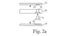
図2aは、セキュリティドキュメント1の面に対して平行な方向から見られた、基層10、電子モジュール4、第1の被覆層11、および第2の被覆層12を示す。基層10は基層10の第1の側から基層10の第2の側に延びる貫通穴15を含む。電子モジュール4は貫通穴15の中に挿入される。電子モジュール4のサイズと形態とは実質的に貫通穴15のサイズと形態とに対応する。第1の被覆層11は基層10の第1の側に隣接して配置され、第2の被覆層12は基層10の第2の側に隣接して配置される。 FIG. 2 a shows the
第1の被覆層11は第1のパッチ21を備え、第1のパッチ21は、基層10の第1の側を向く、第1の被覆層11の側にホットスタンピングされる。第2の被覆層12は第2のパッチ22を備え、第2のパッチ22は、基層10の第2の側を向く、第2の被覆層12の側にホットスタンピングされる。ホットスタンピング処理において、第1のパッチ21は加熱したホットスタンピングダイを使用してキャリアフィルムから第1の被覆層11に転移される。第2のパッチ22も同様の方法でキャリアフィルムから第2の被覆層12に転移される。ホットスタンピングは公知の乾式印刷法であるので、ホットスタンピング処理の詳細は本明細書においては説明されない。 The first covering
図2bは完成したセキュリティドキュメント1を示す。第1の被覆層11は基層10の第1の側に付着させられ、第2の被覆層12は基層10の第2の側に付着させられる。一実施形態において、基層10と第1の被覆層11と第2の被覆層12とは互いに積層される。電子モジュール4は第1の被覆層11と第2の被覆層12との間に挟まれる。第1のパッチ21が、基層10の第1の側で、貫通穴15を囲み、貫通穴15の周りの周囲領域を被覆することにより、周囲領域において第1の被覆層11に基層10の第1の側が付着するのを防ぐように、第1のパッチ21は寸法を合わされて位置決めされる。第2のパッチ22が、基層10の第2の側で、貫通穴15を囲み、貫通穴15の周りの周囲領域を被覆することにより、周囲領域において第2の被覆層12に基層10の第2の側が付着するのを防ぐように、第2のパッチ22は寸法を合わされて位置決めされる。 FIG. 2 b shows the completed
図2cは、第2のパッチ22の面に対して垂直な方向から、貫通穴15および第2のパッチ22を示す。第2のパッチ22の面積は貫通穴15の面積よりも大きく、第2のパッチ22の周囲が貫通穴15を囲むように第2のパッチ22は位置決めされる。貫通穴15の周りの周囲領域は参照番号54で示され、周囲領域の幅はWpaで示される。FIG. 2 c shows the through
図2aおよび図2bは、電子モジュール4の面積が、基層10の第2の側よりも基層10の第1の側において小さいことを示す。また、第1のパッチ21の面積も第2のパッチ22の面積よりも小さい。代替の実施形態においては、電子モジュールの面積が基層の第2の側よりも基層の第1の側において小さかったとしても、第1のパッチの面積と第2のパッチの面積とは等しい。前記代替の実施形態において、周囲領域の幅は基層の第2の側よりも基層の第1の側において大きい。 2a and 2b show that the area of the
第1のパッチ21は透明な熱可塑性材料であるポリメチルメタクリレートで作られた薄箔である。第1のパッチ21の厚さは1〜5μmであり得る。代替の実施形態において、ポリエチレンテレフタラート(PET)または他の熱可塑性材料が使用されてもよい。さらなる代替の実施形態において、第1のパッチはアルミニウム箔、銅箔、または銀箔などの金属箔を備えてもよい。例えば、少なくとも1つの熱可塑性箔と少なくとも1つの金属箔とを備える積層または複合材料から第1のパッチを製造することによって上記の材料を組み合わせることも可能である。 The
代替の実施形態において、第1のパッチの厚さは5μmよりもかなり大きくてもよい。技術的には、20μmまたはさらに大きな厚さを有する第1のパッチを使用することが完全に可能である。しかしながら、厚い第1のパッチは視覚的に検知可能であり、このことは、多くの場合において、悪い特徴となる。 In an alternative embodiment, the thickness of the first patch may be significantly greater than 5 μm. Technically it is entirely possible to use a first patch having a thickness of 20 μm or even larger. However, the thick first patch is visually detectable, which is often a bad feature.
第2のパッチ22の材料および厚さは第1のパッチ21の材料および厚さと同一であってもよい。代替の実施形態において、第2のパッチ22の厚さは第1のパッチ21の厚さと異なってもよく、および/または第2のパッチ22の材料は第1のパッチ21の材料と異なってもよい。 The material and thickness of the
図3aおよび図3はセキュリティドキュメントを製造する代替の方法を示す。この代替の方法において、パッチは被覆層にホットスタンピングされないが、電子モジュールを備える基層にホットスタンピングされる。 Figures 3a and 3 show an alternative method of producing a security document. In this alternative method, the patch is not hot stamped on the covering layer, but is hot stamped on the base layer comprising the electronic module.
図3aは、基層10’、電子モジュール4’、第1の被覆層11’、および第2の被覆層12’を示す。基層10’は、基層10’の第1の側から基層10’の第2の側に延びる貫通穴15’を含む。電子モジュール4’は貫通穴15’の中に既に挿入されている。電子モジュール4’のサイズおよび形態は実質的に貫通穴15’のサイズおよび形態に対応する。 FIG. 3a shows a base layer 10 ', an electronic module 4', a first coating layer 11 ', and a second coating layer 12'. The base layer 10 'includes a through hole 15' extending from the first side of the base layer 10 'to the second side of the base layer 10'. The electronic module 4 'has already been inserted into the through hole 15'. The size and configuration of the electronic module 4 'substantially corresponds to the size and configuration of the through hole 15'.
基層10’は第1のパッチ21’を備え、第1のパッチ21’は第1の被覆層11’に向く、基層10’の側にホットスタンピングされる。基層10’はまた第2のパッチ22’を備え、第2のパッチ22’は第2の被覆層12’に向く、基層10’の側にホットスタンピングされる。 The
電子モジュール4’は第1のパッチ21’と第2のパッチ22’との間に位置決めされる。電子モジュール4’は保護層44’を備え、保護層44’は、電子モジュール4’の第1の側および第2の側の両方で延びる。第1の側は第1の被覆層11’に向く側であり、第2の側は第2の被覆層12’に向く側である。保護層44’は貫通穴15’の中に電子モジュール4’を挿入する前に電子モジュール4’上に提供される。あるいは、電子モジュールが貫通穴に挿入された後に電子モジュール上に保護層を提供することが可能である。保護層44’は基層10’上に第1のパッチ21’および第2のパッチ22’を提供するために使用されるホットスタンピング処理の間に電子モジュール4’を保護するように適合される。保護層44’はポリカーボネートを備えてもよい。 The electronic module 4 'is positioned between the first patch 21' and the second patch 22 '. The electronic module 4 'includes a protective layer 44', which extends on both the first side and the second side of the electronic module 4 '. The first side is the side facing the
代替の実施形態において、電子モジュールは、電子モジュールの一方側だけに保護層を備える。例えば、電子モジュールの一方側が電子モジュールの他方側よりも熱および/または圧力に耐えることが出来ない時に、一方側だけの保護層が使用されてもよい。 In an alternative embodiment, the electronic module comprises a protective layer on only one side of the electronic module. For example, a protective layer on only one side may be used when one side of the electronic module cannot withstand heat and / or pressure more than the other side of the electronic module.
保護層は面積が第1のパッチの面積よりも実質的に大きい層であってもよい。一実施形態において、保護層の面積はセキュリティドキュメントの面積と同じである。 The protective layer may be a layer whose area is substantially larger than the area of the first patch. In one embodiment, the area of the protective layer is the same as the area of the security document.
電子モジュールの膨張および収縮が電子モジュールに近い場所で保護層に何らかの亀裂をもたらし得る。しかしながら、保護層と被覆層との間のパッチは亀裂がセキュリティドキュメントの外面に向かって進むのを防ぐ。 The expansion and contraction of the electronic module can cause some cracks in the protective layer near the electronic module. However, the patch between the protective layer and the covering layer prevents the crack from progressing towards the outer surface of the security document.
図3bは完成したセキュリティドキュメント1’を示す。第1の被覆層11’は基層10’の第1の側に付着させられ、第2の被覆層12’は基層10’の第2の側に付着させられる。電子モジュール4’は第1の被覆層11’と第2の被覆層12’との間に挟まれる。第1のパッチ21’が、基層10’の第1の側で、貫通穴15’を囲み、貫通穴15’の周りの周囲領域を被覆することにより、周囲領域において、第1の被覆層11’に基層10’の第1の側が付着するのを防ぐように、第1のパッチ21’は寸法を合わされて位置決めされる。第2のパッチ22’が、基層10’の第2の側で、貫通穴15’を囲み、貫通穴15’の周りの周囲領域を被覆することにより、周囲領域において、第2の被覆層12’に基層10’の第2の側が付着するのを防ぐように、第2のパッチ22’は寸法を合わされて位置決めされる。 FIG. 3b shows the completed security document 1 '. The first coating layer 11 'is deposited on the first side of the base layer 10' and the second coating layer 12 'is deposited on the second side of the base layer 10'. The electronic module 4 'is sandwiched between the first coating layer 11' and the second coating layer 12 '. A
基層10’の第1の側における電子モジュール4’の表面積は、基層10’の第2の側における電子モジュール4’の表面積と等しい。したがって、第1のパッチ21’の面積は、第2のパッチ22’の面積と等しい。 The surface area of the electronic module 4 'on the first side of the base layer 10' is equal to the surface area of the electronic module 4 'on the second side of the base layer 10'. Accordingly, the area of the first patch 21 'is equal to the area of the second patch 22'.
さらなる代替の実施形態において、保護層を有さない電子モジュールを含む基層にパッチがホットスタンピングされる。当然、この実施形態は、耐熱性および耐圧性が充分にある電子モジュールを必要とする。 In a further alternative embodiment, the patch is hot stamped onto a base layer comprising an electronic module without a protective layer. Of course, this embodiment requires an electronic module with sufficient heat resistance and pressure resistance.
図2bのセキュリティドキュメントと図3bのセキュリティドキュメントとの両方が、基層の第1の側における第1のパッチと、基層の第2の側における第2のパッチとを備える。あるいは、基層の一方側だけにパッチを有するセキュリティドキュメントを提供することが可能である。 Both the security document of FIG. 2b and the security document of FIG. 3b comprise a first patch on the first side of the base layer and a second patch on the second side of the base layer. Alternatively, it is possible to provide a security document with a patch on only one side of the base layer.
本発明の概念は様々な方法で実装されることが出来ることが当業者には明らかである。本発明および本発明の実施形態は上記の例に限定されず、特許請求の範囲の範囲内で変わり得る。 It will be apparent to those skilled in the art that the concepts of the present invention can be implemented in a variety of ways. The invention and embodiments of the invention are not limited to the examples described above but may vary within the scope of the claims.
Claims (13)
Translated fromJapanese基層(10、10’)の第1の側に付着させられた第1の被覆層(11、11’)と、
基層(10、10’)の第2の側に付着させられた第2の被覆層(12、12’)と、
前記貫通穴(15、15’)に配置された電子モジュール(4、4’)と
を備えるセキュリティドキュメント(1、1’)であって、
セキュリティドキュメント(1、1’)は、基層(10、10’)と第1の被覆層(11、11’)との間にホットスタンピングして位置決めされることによってセキュリティドキュメント(1、1’)に付着させられた第1のパッチ(21、21’)をさらに備え、第1のパッチ(21、21’)は、基層(10、10’)の第1の側において、貫通穴(15、15’)を囲み、貫通穴(15、15’)の周りの周囲領域を被覆することにより、周囲領域の範囲において第1の被覆層(11、11’)に基層(10、10’)が付着するのを防ぐことを特徴とする、セキュリティドキュメント(1、1’)。A base layer (10, 10 ') having a through hole (15, 15') extending from a first side of the base layer (10, 10 ') to a second side of the base layer (10, 10');
A first covering layer (11, 11 ') deposited on the first side of the base layer (10, 10');
A second covering layer (12, 12 ') deposited on the second side of the base layer (10, 10');
A security document (1, 1 ') comprising an electronic module (4, 4') disposed in the through hole (15, 15 '),
The security document (1, 1 ′) is positioned by hot stamping between the base layer (10, 10 ′) and the first covering layer (11, 11 ′). The first patch (21, 21 ') is attached to the first layer (21, 21') on the first side of the base layer (10, 10 '). 15 ′) and covering the surrounding area around the through hole (15, 15 ′), the base layer (10, 10 ′) is formed on the first covering layer (11, 11 ′) in the area of the surrounding area. Security document (1, 1 '), characterized by preventing sticking.
前記貫通穴(15、15’)に電子モジュール(4、4’)を配置するステップと、
基層(10、10’)が第1の被覆層(11、11’)と第2の被覆層(12、12’)との間に挟まれるように、基層(10、10’)と第1の被覆層(11、11’)と第2の被覆層(12、12’)とを互いに付着させるステップと
を含む、セキュリティドキュメント(1、1’)を製造する方法であって、
方法は、
第1のパッチ(21、21’)を提供するステップと、
完成したセキュリティドキュメント(1、1’)において、第1のパッチ(21、21’)が、基層(10、10’)の第1の側において、貫通穴(15、15’)を囲み、貫通穴(15、15’)の周りの周囲領域を被覆することにより、周囲領域の範囲において第1の被覆層(11、11’)に基層(10、10’)が付着するのを防ぐようにホットスタンピングすることによって基層(10、10’)と第1の被覆層(11、11’)との間に第1のパッチ(21、21’)を付着させるステップと
をさらに含むことを特徴とする、方法。Providing a base layer (10, 10 '), a first coating layer (11, 11'), a second coating layer (12, 12 '), and an electronic module (4, 4'). The base layer (10, 10 ′) has a through hole (15, 15 ′) extending from a first side of the base layer (10, 10 ′) to a second side of the base layer (10, 10 ′). And steps to
Placing an electronic module (4, 4 ') in the through hole (15, 15');
The base layer (10, 10 ′) and the first layer are sandwiched between the first cover layer (11, 11 ′) and the second cover layer (12, 12 ′). A security document (1, 1 ') comprising the steps of: attaching a covering layer (11, 11') and a second covering layer (12, 12 ') to each other,
The method is
Providing a first patch (21, 21 ');
In the completed security document (1, 1 ′), the first patch (21, 21 ′) surrounds and penetrates the through hole (15, 15 ′) on the first side of the base layer (10, 10 ′). By covering the surrounding area around the hole (15, 15 ′), the base layer (10, 10 ′) is prevented from adhering to the first covering layer (11, 11 ′) in the area of the surrounding area. Attaching a first patch (21, 21 ') between the base layer (10, 10') and the first covering layer (11, 11 ') by hot stamping, how to.
電子モジュール(4’)上に保護層(44’)を提供するステップであって、前記保護層(44’)はホットスタンピング処理の間に電子モジュール(4’)を保護するように適合される、提供するステップと、続いて、貫通穴(15’)に電子モジュール(4’)を挿入するステップと
をさらに含み、
電子モジュール(4’)が貫通穴(15’)にある間に、第1のパッチ(21’)は基層(10’)にホットスタンピングされることを特徴とする、請求項9に記載の方法。The method is
Providing a protective layer (44 ') on the electronic module (4'), said protective layer (44 ') being adapted to protect the electronic module (4') during a hot stamping process Providing a step followed by inserting an electronic module (4 ') into the through hole (15');
Method according to claim 9, characterized in that the first patch (21 ') is hot stamped onto the base layer (10') while the electronic module (4 ') is in the through hole (15'). .
Applications Claiming Priority (3)
| Application Number | Priority Date | Filing Date | Title |
|---|---|---|---|
| EP10306339.2 | 2010-12-02 | ||
| EP10306339AEP2461275A1 (en) | 2010-12-02 | 2010-12-02 | Security Document and method of manufacturing security document |
| PCT/EP2011/071237WO2012072610A1 (en) | 2010-12-02 | 2011-11-29 | Security document and method of manufacturing security document |
Publications (2)
| Publication Number | Publication Date |
|---|---|
| JP2014503386Atrue JP2014503386A (en) | 2014-02-13 |
| JP5941057B2 JP5941057B2 (en) | 2016-06-29 |
Family
ID=44021820
Family Applications (1)
| Application Number | Title | Priority Date | Filing Date |
|---|---|---|---|
| JP2013541319AExpired - Fee RelatedJP5941057B2 (en) | 2010-12-02 | 2011-11-29 | How to produce security documents |
Country Status (9)
| Country | Link |
|---|---|
| US (1) | US9858522B2 (en) |
| EP (2) | EP2461275A1 (en) |
| JP (1) | JP5941057B2 (en) |
| CN (1) | CN103339643B (en) |
| BR (1) | BR112013013611A2 (en) |
| DK (1) | DK2646954T3 (en) |
| ES (1) | ES2533651T3 (en) |
| PT (1) | PT2646954E (en) |
| WO (1) | WO2012072610A1 (en) |
Families Citing this family (3)
| Publication number | Priority date | Publication date | Assignee | Title |
|---|---|---|---|---|
| EP2461275A1 (en)* | 2010-12-02 | 2012-06-06 | Gemalto SA | Security Document and method of manufacturing security document |
| WO2014045139A1 (en) | 2012-09-18 | 2014-03-27 | Assa Abloy Ab | Method of protecting an electrical component in a laminate |
| CN110901255B (en)* | 2019-12-20 | 2023-08-01 | 公安部交通管理科学研究所 | Anti-counterfeit card with asymmetric structure and its manufacturing method |
Citations (4)
| Publication number | Priority date | Publication date | Assignee | Title |
|---|---|---|---|---|
| JPH1024684A (en)* | 1996-07-10 | 1998-01-27 | Dainippon Printing Co Ltd | IC card |
| JPH10147088A (en)* | 1996-11-20 | 1998-06-02 | Dainippon Printing Co Ltd | Non-contact type IC card and manufacturing method thereof |
| JP2004341720A (en)* | 2003-05-14 | 2004-12-02 | Toshiba Corp | Wireless card |
| JP2010160756A (en)* | 2009-01-09 | 2010-07-22 | Toshiba Corp | IC card |
Family Cites Families (60)
| Publication number | Priority date | Publication date | Assignee | Title |
|---|---|---|---|---|
| US4906315A (en)* | 1983-06-20 | 1990-03-06 | Mcgrew Stephen P | Surface relief holograms and holographic hot-stamping foils, and method of fabricating same |
| DE3338597A1 (en)* | 1983-10-24 | 1985-05-02 | GAO Gesellschaft für Automation und Organisation mbH, 8000 München | DATA CARRIER WITH INTEGRATED CIRCUIT AND METHOD FOR PRODUCING THE SAME |
| US4727246A (en)* | 1984-08-31 | 1988-02-23 | Casio Computer Co., Ltd. | IC card |
| JPH0751390B2 (en)* | 1985-07-10 | 1995-06-05 | カシオ計算機株式会社 | IC card |
| JPH0716094B2 (en)* | 1986-03-31 | 1995-02-22 | 日立化成工業株式会社 | Wiring board manufacturing method |
| JPH0696357B2 (en)* | 1986-12-11 | 1994-11-30 | 三菱電機株式会社 | IC card manufacturing method |
| JPH01136792A (en)* | 1987-11-25 | 1989-05-30 | Dainippon Printing Co Ltd | IC card |
| JPH01152098A (en)* | 1988-09-08 | 1989-06-14 | Dainippon Printing Co Ltd | Card base material for ic card |
| DE69317180T2 (en)* | 1992-08-28 | 1998-10-08 | Citizen Watch Co Ltd | Process for the production of IC cards |
| DE4317184C1 (en)* | 1993-05-22 | 1994-07-07 | Melzer Maschinenbau Gmbh | Smart card mfr. e.g. for credit, debit esp. telephone card |
| TW272311B (en)* | 1994-01-12 | 1996-03-11 | At & T Corp | |
| EP0786357A4 (en)* | 1994-09-22 | 2000-04-05 | Rohm Co Ltd | Non-contact type ic card and method of manufacturing same |
| JP4015717B2 (en)* | 1995-06-29 | 2007-11-28 | 日立マクセル株式会社 | Information carrier manufacturing method |
| DE19602821C1 (en)* | 1996-01-26 | 1997-06-26 | Siemens Ag | Method for producing a data card |
| EP0938412B1 (en)* | 1996-11-12 | 2004-02-11 | NagraID S.A. | Method for making cards |
| EP0919950B1 (en)* | 1997-06-23 | 2007-04-04 | Rohm Co., Ltd. | Module for ic card, ic card, and method for manufacturing module for ic card |
| DE19731983A1 (en)* | 1997-07-24 | 1999-01-28 | Giesecke & Devrient Gmbh | Contactlessly operated data carrier |
| US6331208B1 (en)* | 1998-05-15 | 2001-12-18 | Canon Kabushiki Kaisha | Process for producing solar cell, process for producing thin-film semiconductor, process for separating thin-film semiconductor, and process for forming semiconductor |
| SG80077A1 (en)* | 1998-10-19 | 2001-04-17 | Sony Corp | Semiconductor integrated circuit card manufacturing method, and semiconductor integrated circuit card |
| US6239976B1 (en)* | 1998-11-24 | 2001-05-29 | Comsense Technologies, Ltd. | Reinforced micromodule |
| JP2000349178A (en)* | 1999-06-08 | 2000-12-15 | Mitsubishi Electric Corp | Semiconductor device and manufacturing method thereof |
| US6885291B1 (en)* | 1999-11-15 | 2005-04-26 | The Goodyear Tire & Rubber Company | Mouting transponders and antennas in pneumatic tires |
| KR100335716B1 (en)* | 2000-05-23 | 2002-05-08 | 윤종용 | Memory Card |
| US6475327B2 (en)* | 2001-04-05 | 2002-11-05 | Phoenix Precision Technology Corporation | Attachment of a stiff heat spreader for fabricating a cavity down plastic chip carrier |
| JP3478281B2 (en)* | 2001-06-07 | 2003-12-15 | ソニー株式会社 | IC card |
| US6537852B2 (en)* | 2001-08-22 | 2003-03-25 | International Business Machines Corporation | Spacer - connector stud for stacked surface laminated multichip modules and methods of manufacture |
| US6644551B2 (en)* | 2001-11-09 | 2003-11-11 | G + D Cardtech, Inc. | Card |
| CA2469956C (en)* | 2001-12-24 | 2009-01-27 | Digimarc Id Systems, Llc | Contact smart cards having a document core, contactless smart cards including multi-layered structure, pet-based identification document, and methods of making same |
| JP2003331242A (en)* | 2002-05-10 | 2003-11-21 | Konica Minolta Holdings Inc | Ic card |
| JP4060653B2 (en)* | 2002-07-12 | 2008-03-12 | 大日本印刷株式会社 | Non-contact IC card |
| FR2844621A1 (en)* | 2002-09-13 | 2004-03-19 | A S K | Method for manufacturing without contact or hybrid integrated circuit card, comprises application of two thermoplastic layers under temperature and pressure followed by two hot pressed plastic layers |
| JP2004185208A (en)* | 2002-12-02 | 2004-07-02 | Sony Corp | Ic card |
| US7143953B2 (en)* | 2002-12-27 | 2006-12-05 | Konica Minolta Holdings, Inc. | IC card, IC card manufacturing method, IC card manufacturing apparatus and IC card judgement system |
| JP4052967B2 (en)* | 2003-03-25 | 2008-02-27 | 富士通株式会社 | Antenna coupling module |
| DE10316771A1 (en)* | 2003-04-10 | 2004-10-28 | Giesecke & Devrient Gmbh | Security label and manufacturing process for the same |
| JP4479209B2 (en)* | 2003-10-10 | 2010-06-09 | パナソニック株式会社 | Electronic circuit device, method for manufacturing the same, and apparatus for manufacturing electronic circuit device |
| JP2005234683A (en)* | 2004-02-17 | 2005-09-02 | Matsushita Electric Ind Co Ltd | IC card |
| JP4676196B2 (en)* | 2004-12-16 | 2011-04-27 | 富士通株式会社 | RFID tag |
| TWM274641U (en)* | 2005-04-01 | 2005-09-01 | Lingsen Precision Ind Ltd | Packaging carrier for integrated circuit |
| NL1029985C2 (en)* | 2005-09-20 | 2007-03-21 | Sdu Identification Bv | Identity document with chip. |
| KR100723635B1 (en)* | 2005-12-08 | 2007-06-04 | 한국전자통신연구원 | Conversion circuit for transmitting high frequency signal and transmitting / receiving module having same |
| NL1030865C2 (en)* | 2006-01-06 | 2007-07-09 | Sdu Identification Bv | Identity document with chip. |
| US8608080B2 (en)* | 2006-09-26 | 2013-12-17 | Feinics Amatech Teoranta | Inlays for security documents |
| US20080179404A1 (en)* | 2006-09-26 | 2008-07-31 | Advanced Microelectronic And Automation Technology Ltd. | Methods and apparatuses to produce inlays with transponders |
| EP1914671B1 (en)* | 2006-10-12 | 2011-11-23 | HID Global GmbH | Transponder embedded in a flexible multi-layer support |
| RU2471232C2 (en)* | 2007-09-14 | 2012-12-27 | Топпан Принтинг Ко., Лтд. | Antenna sheet, transponder and booklet |
| EP2053544A1 (en)* | 2007-10-23 | 2009-04-29 | F. Hoffman-la Roche AG | Method for manufacturing a smart label with a laser printable adhesive label |
| EP2116366B1 (en)* | 2008-05-06 | 2015-08-12 | HID Global GmbH | Functional laminate |
| US20150227829A1 (en)* | 2008-08-29 | 2015-08-13 | David Finn | Laminates for security documents |
| PH12012500375A1 (en)* | 2009-08-26 | 2012-10-22 | Toppan Printing Co Ltd | Contactless communication medium |
| KR101291319B1 (en)* | 2009-09-18 | 2013-07-30 | 한국전자통신연구원 | apparatus for generating/detecting THz wave and manufacturing method of the same |
| US8674892B2 (en)* | 2010-06-20 | 2014-03-18 | Siklu Communication ltd. | Accurate millimeter-wave antennas and related structures |
| US8674885B2 (en)* | 2010-08-31 | 2014-03-18 | Siklu Communication ltd. | Systems for interfacing waveguide antenna feeds with printed circuit boards |
| US8608084B2 (en)* | 2010-09-30 | 2013-12-17 | Steve Klaas | Financial card with embedded circuit lock technology |
| EP2461275A1 (en)* | 2010-12-02 | 2012-06-06 | Gemalto SA | Security Document and method of manufacturing security document |
| US9798968B2 (en)* | 2013-01-18 | 2017-10-24 | Féinics Amatech Teoranta | Smartcard with coupling frame and method of increasing activation distance of a transponder chip module |
| FR2979852B1 (en)* | 2011-09-14 | 2013-09-27 | Arjowiggins Security | MULTILAYER STRUCTURE INTEGRATING AT LEAST ONE SAFETY ELEMENT |
| DE102013102718A1 (en)* | 2013-03-18 | 2014-09-18 | Infineon Technologies Ag | Smart card module arrangement |
| US9435856B2 (en)* | 2013-04-16 | 2016-09-06 | Mpi Corporation | Position adjustable probing device and probe card assembly using the same |
| US9470750B2 (en)* | 2013-04-16 | 2016-10-18 | Mpi Corporation | Alignment adjusting mechanism for probe card, position adjusting module using the same and modularized probing device |
- 2010
- 2010-12-02EPEP10306339Apatent/EP2461275A1/ennot_activeWithdrawn
- 2011
- 2011-11-29JPJP2013541319Apatent/JP5941057B2/ennot_activeExpired - Fee Related
- 2011-11-29DKDK11788471.8Tpatent/DK2646954T3/enactive
- 2011-11-29CNCN201180066769.8Apatent/CN103339643B/ennot_activeExpired - Fee Related
- 2011-11-29USUS13/991,167patent/US9858522B2/ennot_activeExpired - Fee Related
- 2011-11-29EPEP11788471.8Apatent/EP2646954B1/ennot_activeNot-in-force
- 2011-11-29WOPCT/EP2011/071237patent/WO2012072610A1/enactiveApplication Filing
- 2011-11-29ESES11788471.8Tpatent/ES2533651T3/enactiveActive
- 2011-11-29PTPT117884718Tpatent/PT2646954E/enunknown
- 2011-11-29BRBR112013013611Apatent/BR112013013611A2/ennot_activeApplication Discontinuation
Patent Citations (4)
| Publication number | Priority date | Publication date | Assignee | Title |
|---|---|---|---|---|
| JPH1024684A (en)* | 1996-07-10 | 1998-01-27 | Dainippon Printing Co Ltd | IC card |
| JPH10147088A (en)* | 1996-11-20 | 1998-06-02 | Dainippon Printing Co Ltd | Non-contact type IC card and manufacturing method thereof |
| JP2004341720A (en)* | 2003-05-14 | 2004-12-02 | Toshiba Corp | Wireless card |
| JP2010160756A (en)* | 2009-01-09 | 2010-07-22 | Toshiba Corp | IC card |
Also Published As
| Publication number | Publication date |
|---|---|
| BR112013013611A2 (en) | 2016-09-06 |
| CN103339643A (en) | 2013-10-02 |
| PT2646954E (en) | 2015-01-05 |
| EP2646954B1 (en) | 2014-10-22 |
| EP2646954A1 (en) | 2013-10-09 |
| WO2012072610A1 (en) | 2012-06-07 |
| JP5941057B2 (en) | 2016-06-29 |
| US9858522B2 (en) | 2018-01-02 |
| US20140175176A1 (en) | 2014-06-26 |
| ES2533651T3 (en) | 2015-04-13 |
| CN103339643B (en) | 2016-07-06 |
| DK2646954T3 (en) | 2014-12-15 |
| EP2461275A1 (en) | 2012-06-06 |
Similar Documents
| Publication | Publication Date | Title |
|---|---|---|
| EP1946253B1 (en) | Smart card producing method and a smart card in particular provided with a magnetic antenna | |
| CN103119616A (en) | Polycarbonate radiofrequency identification device, and method for manufacturing same | |
| KR20090118066A (en) | Inlay manufacturing method and semifinished product for inlay manufacture | |
| JP5941057B2 (en) | How to produce security documents | |
| US9629248B2 (en) | Embedded printed circuit board | |
| EP1842689A2 (en) | Thermally stable proximity indentifaction card | |
| US10455703B2 (en) | Method for producing a printed circuit board with an embedded sensor chip, and printed circuit board | |
| JP2006503424A (en) | Electronic module with visible elements on the surface and method for manufacturing such a module | |
| CN100544556C (en) | Multilayer printed circuit board and manufacture method thereof | |
| EP1969536A1 (en) | Identity document having a chip | |
| JP2005004430A (en) | Non-contact IC card and IC module | |
| US8772912B2 (en) | Electronic device | |
| CN101651108B (en) | Soft film chip-on-die encapsulation process | |
| JP5708137B2 (en) | Non-contact information media and booklet attached to non-contact information media | |
| CN112760052A (en) | Composite adhesive tape, processing method of composite adhesive tape and flexible screen module | |
| US9392734B1 (en) | Security wrapper for an electronic assembly and methods for forming such a wrapper | |
| JP7506543B2 (en) | Element protection structure and manufacturing method thereof | |
| JP6844232B2 (en) | Non-contact communication medium for booklet and booklet | |
| EP3742875A1 (en) | Thermal management in an electronic device | |
| EP1231076B1 (en) | Laminated structure | |
| KR20210124840A (en) | Electric assembly including heat spreader | |
| FR2855890A1 (en) | Multilayer card e.g. bank card, for data support, has reinforced connection zones extending across printed layer in vicinity of intersection of adjacent card edges, where each zone is soldered to corresponding portion of layer | |
| US20140346686A1 (en) | Methods for forming color images on memory devices and memory devices formed thereby | |
| JP6184337B2 (en) | IC card and manufacturing method thereof | |
| KR102159548B1 (en) | Embedded printed circuit substrate |
Legal Events
| Date | Code | Title | Description |
|---|---|---|---|
| A621 | Written request for application examination | Free format text:JAPANESE INTERMEDIATE CODE: A621 Effective date:20141031 | |
| A977 | Report on retrieval | Free format text:JAPANESE INTERMEDIATE CODE: A971007 Effective date:20151218 | |
| A131 | Notification of reasons for refusal | Free format text:JAPANESE INTERMEDIATE CODE: A131 Effective date:20160105 | |
| A521 | Request for written amendment filed | Free format text:JAPANESE INTERMEDIATE CODE: A523 Effective date:20160330 | |
| TRDD | Decision of grant or rejection written | ||
| A01 | Written decision to grant a patent or to grant a registration (utility model) | Free format text:JAPANESE INTERMEDIATE CODE: A01 Effective date:20160510 | |
| A61 | First payment of annual fees (during grant procedure) | Free format text:JAPANESE INTERMEDIATE CODE: A61 Effective date:20160519 | |
| R150 | Certificate of patent or registration of utility model | Ref document number:5941057 Country of ref document:JP Free format text:JAPANESE INTERMEDIATE CODE: R150 | |
| R250 | Receipt of annual fees | Free format text:JAPANESE INTERMEDIATE CODE: R250 | |
| LAPS | Cancellation because of no payment of annual fees |