JP2014241424A - Semiconductor device - Google Patents
Semiconductor deviceDownload PDFInfo
- Publication number
- JP2014241424A JP2014241424AJP2014150498AJP2014150498AJP2014241424AJP 2014241424 AJP2014241424 AJP 2014241424AJP 2014150498 AJP2014150498 AJP 2014150498AJP 2014150498 AJP2014150498 AJP 2014150498AJP 2014241424 AJP2014241424 AJP 2014241424A
- Authority
- JP
- Japan
- Prior art keywords
- layer
- thin film
- wiring
- film transistor
- oxide semiconductor
- Prior art date
- Legal status (The legal status is an assumption and is not a legal conclusion. Google has not performed a legal analysis and makes no representation as to the accuracy of the status listed.)
- Withdrawn
Links
Images


Landscapes
- Thin Film Transistor (AREA)
- Liquid Crystal (AREA)
- Electroluminescent Light Sources (AREA)
- Metal-Oxide And Bipolar Metal-Oxide Semiconductor Integrated Circuits (AREA)
- Electrochromic Elements, Electrophoresis, Or Variable Reflection Or Absorption Elements (AREA)
- Shift Register Type Memory (AREA)
- Internal Circuitry In Semiconductor Integrated Circuit Devices (AREA)
- Devices For Indicating Variable Information By Combining Individual Elements (AREA)
Abstract
Description
Translated fromJapanese本発明は、酸化物半導体を用いる表示装置及びその製造方法に関する。The present invention relates to a display device using an oxide semiconductor and a manufacturing method thereof.
液晶表示装置に代表されるように、ガラス基板等の平板に形成される薄膜トランジスタは
、アモルファスシリコン、多結晶シリコンによって作製されている。アモルファスシリコ
ンを用いた薄膜トランジスタは、電界効果移動度が低いもののガラス基板の大面積化に対
応することができ、一方、結晶シリコンを用いた薄膜トランジスタは電界効果移動度が高
いものの、レーザアニール等の結晶化工程が必要であり、ガラス基板の大面積化には必ず
しも適応しないといった特性を有している。As represented by a liquid crystal display device, a thin film transistor formed on a flat plate such as a glass substrate is made of amorphous silicon or polycrystalline silicon. A thin film transistor using amorphous silicon can cope with an increase in the area of a glass substrate although the field effect mobility is low. On the other hand, a thin film transistor using crystalline silicon has a high field effect mobility, but crystal such as laser annealing. Therefore, it has a characteristic that it is not necessarily adapted to increase the area of the glass substrate.
これに対し、酸化物半導体を用いて薄膜トランジスタを作製し、電子デバイスや光デバイ
スに応用する技術が注目されている。例えば、酸化物半導体層として酸化亜鉛、In−G
a−Zn−O系酸化物半導体を用いて薄膜トランジスタを作製し、表示装置のスイッチン
グ素子などに用いる技術が特許文献1、特許文献2、及び非特許文献1で開示されている
。In contrast, a technique in which a thin film transistor is manufactured using an oxide semiconductor and applied to an electronic device or an optical device has attracted attention. For example, zinc oxide, In-G as the oxide semiconductor layer
しかしながら、酸化物半導体層を用いた薄膜トランジスタにおいて、酸化物半導体層のパ
ッシベーション層として、シラン、二酸化窒素、アンモニア、窒素等のいずれかを原料ガ
スとしたプラズマCVD法を用いて形成した窒化珪素層、または酸化珪素層を用いると、
薄膜トランジスタの電気特性の信頼性が低減するという問題がある。However, in a thin film transistor using an oxide semiconductor layer, as a passivation layer of the oxide semiconductor layer, a silicon nitride layer formed using a plasma CVD method using any one of silane, nitrogen dioxide, ammonia, nitrogen, or the like as a source gas, Or when using a silicon oxide layer,
There is a problem that reliability of electric characteristics of the thin film transistor is reduced.
そこで、薄膜トランジスタの電気特性の信頼性を高めることが可能な薄膜トランジスタ及
びその作製方法を提供することを課題の一つとする。また、画質を向上させることが可能
な表示装置及びその作製方法を提供することを課題の一つとする。Thus, it is an object to provide a thin film transistor that can improve the reliability of electric characteristics of the thin film transistor and a manufacturing method thereof. Another object is to provide a display device capable of improving image quality and a manufacturing method thereof.
ゲート電極と、ゲート電極に重畳する酸化物半導体層と、酸化物半導体層に接する有機樹
脂層と、酸化物半導体層及び有機樹脂層の間に設けられる配線とを有する薄膜トランジス
タである。The thin film transistor includes a gate electrode, an oxide semiconductor layer overlapping with the gate electrode, an organic resin layer in contact with the oxide semiconductor layer, and a wiring provided between the oxide semiconductor layer and the organic resin layer.
また、ゲート電極と、ゲート電極上に形成されるゲート絶縁層と、ゲート電極に重畳し、
且つゲート絶縁層上に形成される酸化物半導体層と、ゲート絶縁層及び酸化物半導体層上
に形成される配線と、酸化物半導体層及び配線に接する有機樹脂層とを有する薄膜トラン
ジスタである。A gate electrode, a gate insulating layer formed on the gate electrode, and the gate electrode,
In addition, the thin film transistor includes an oxide semiconductor layer formed over the gate insulating layer, a wiring formed over the gate insulating layer and the oxide semiconductor layer, and an organic resin layer in contact with the oxide semiconductor layer and the wiring.
また、上記薄膜トランジスタを駆動回路及び画素部に有する表示装置である。In addition, the display device includes the thin film transistor in a driver circuit and a pixel portion.
なお、酸化物半導体層は、InMO3(ZnO)m(m>0)で表記される薄膜であり、
Mは、ガリウム(Ga)、鉄(Fe)、ニッケル(Ni)、マンガン(Mn)及びコバル
ト(Co)から選ばれた一の金属元素または複数の金属元素を示す。例えばMとして、G
aの場合があることの他、GaとNiまたはGaとFeなど、Ga以外の上記金属元素が
含まれる場合がある。また、上記酸化物半導体層において、Mとして含まれる金属元素の
他に、不純物元素としてFe、Niその他の遷移金属元素、または該遷移金属の酸化物が
含まれているものがある。ここでは、当該薄膜のうちM=ガリウム(Ga)のものをIn
−Ga−Zn−O系非単結晶層とも呼ぶ。Note that the oxide semiconductor layer is a thin film represented by InMO3 (ZnO)m (m> 0),
M represents one metal element or a plurality of metal elements selected from gallium (Ga), iron (Fe), nickel (Ni), manganese (Mn), and cobalt (Co). For example, as M, G
In addition to the case of “a”, the metal element other than Ga, such as Ga and Ni or Ga and Fe, may be contained. In addition to the metal element included as M, the oxide semiconductor layer may include Fe, Ni, other transition metal elements, or an oxide of the transition metal as an impurity element. Here, M = gallium (Ga) of the thin film is In.
Also referred to as a —Ga—Zn—O-based non-single-crystal layer.
In−Ga−Zn−O系非単結晶層の結晶構造は、スパッタリング法で形成した後、20
0℃〜500℃、代表的には300〜400℃で10分〜100分の加熱を行っても、ア
モルファス構造がXRD(X線回析)測定で観察される。また、In−Ga−Zn−O系
非単結晶層用いることで、ゲート電圧±20Vにおいて、オン・オフ比が109以上、移
動度が10cm2/Vs以上の電気特性を有する薄膜トランジスタを作製することができ
る。The crystal structure of the In—Ga—Zn—O-based non-single-crystal layer is 20
Even if heating is performed at 0 to 500 ° C., typically 300 to 400 ° C. for 10 to 100 minutes, an amorphous structure is observed by XRD (X-ray diffraction) measurement. Further, by using an In—Ga—Zn—O-based non-single-crystal layer, a thin film transistor having an electrical property with an on / off ratio of 109 or more and a mobility of 10 cm2 / Vs or more at a gate voltage of ± 20 V is manufactured. be able to.
このような電気特性を有する薄膜トランジスタを駆動回路に用いることは有用である。例
えば、ゲート線駆動回路は、ゲート信号を順次転送するシフトレジスタ回路と、バッファ
回路などで構成され、ソース線駆動回路は、ゲート信号を順次転送するシフトレジスタと
、バッファ回路と、画素への映像信号の転送のオン・オフを切り替えるアナログスイッチ
などにより構成される。アモルファスシリコンを用いた薄膜トランジスタに比べ高い移動
度を有する酸化物半導体層を用いた薄膜トランジスタは、シフトレジスタ回路を高速駆動
させることができる。It is useful to use a thin film transistor having such electrical characteristics for a driver circuit. For example, the gate line driver circuit includes a shift register circuit that sequentially transfers gate signals and a buffer circuit, and the source line driver circuit includes a shift register that sequentially transfers gate signals, a buffer circuit, and an image to a pixel. It consists of an analog switch that switches on / off of signal transfer. A thin film transistor using an oxide semiconductor layer having higher mobility than a thin film transistor using amorphous silicon can drive a shift register circuit at high speed.
また、画素部を駆動する駆動回路の少なくとも一部の回路を酸化物半導体を用いた薄膜ト
ランジスタで構成する場合、全てnチャネル型TFTで形成され、図1(B)に示した回
路を基本単位として形成する。また、駆動回路において、ゲート電極とソース配線、或い
はドレイン配線を直接接続させることにより、良好なコンタクトを得ることができ、接触
抵抗を低減することができる。駆動回路において、ゲート電極とソース配線、或いはドレ
イン配線を他の導電層、例えば透明導電層を介して接続する場合、コンタクトホールの数
の増加、コンタクトホールの数の増加による占有面積の増大、または接触抵抗及び配線抵
抗の増大、さらには工程の複雑化を招く恐れがある。In the case where at least part of a driver circuit for driving the pixel portion is formed using a thin film transistor including an oxide semiconductor, the driver circuit is formed using n-channel TFTs, and the circuit illustrated in FIG. 1B is used as a basic unit. Form. In the driver circuit, a good contact can be obtained and contact resistance can be reduced by directly connecting the gate electrode and the source wiring or the drain wiring. In the driving circuit, when the gate electrode and the source wiring or the drain wiring are connected through another conductive layer, for example, a transparent conductive layer, the number of contact holes increases, the occupied area increases due to the increase in the number of contact holes, or There is a possibility that the contact resistance and the wiring resistance increase, and further the process becomes complicated.
また、薄膜トランジスタは静電気などにより破壊されやすいため、ゲート線またはソース
線に対して、駆動回路保護用の保護回路を同一基板上に設けることが好ましい。保護回路
は、酸化物半導体を用いた非線形素子を用いて構成することが好ましい。In addition, since the thin film transistor is easily broken by static electricity or the like, it is preferable to provide a protective circuit for protecting the driver circuit over the same substrate for the gate line or the source line. The protection circuit is preferably formed using a non-linear element using an oxide semiconductor.
なお、第1、第2として付される序数詞は便宜上用いるものであり、工程順または積層順
を示すものではない。また、本明細書において発明を特定するための事項として固有の名
称を示すものではない。The ordinal numbers attached as the first and second are used for convenience and do not indicate the order of steps or the order of lamination. In addition, a specific name is not shown as a matter for specifying the invention in this specification.
また、駆動回路を有する表示装置としては、液晶表示装置の他に、発光素子を用いた発光
表示装置や、電気泳動表示素子を用いた電子ペーパーとも称される表示装置がある。In addition to a liquid crystal display device, a display device including a driver circuit includes a light-emitting display device using a light-emitting element and a display device also called electronic paper using an electrophoretic display element.
発光素子を用いた発光表示装置においては、画素部に複数の薄膜トランジスタを有し、画
素部においてもある薄膜トランジスタのゲート電極と他の薄膜トランジスタのソース配線
、或いはドレイン配線を直接接続させる箇所を有している。また、発光素子を用いた発光
表示装置の駆動回路においては、薄膜トランジスタのゲート電極とその薄膜トランジスタ
のソース配線、或いはドレイン配線を直接接続させる箇所を有している。A light-emitting display device using a light-emitting element includes a plurality of thin film transistors in a pixel portion, and a portion in which a gate electrode of a thin film transistor in the pixel portion is directly connected to a source wiring or a drain wiring of another thin film transistor. Yes. In addition, a driver circuit of a light-emitting display device using a light-emitting element has a portion where a gate electrode of a thin film transistor and a source wiring or a drain wiring of the thin film transistor are directly connected.
酸化物半導体を用いた薄膜トランジスタにおいて、酸化物半導体に接する有機絶縁層を形
成することにより、電気特性の信頼性の高い薄膜トランジスタを作製することができる。
また、画質が向上した表示装置を作製することができる。In a thin film transistor using an oxide semiconductor, a thin film transistor with high electrical characteristics can be manufactured by forming an organic insulating layer in contact with the oxide semiconductor.
In addition, a display device with improved image quality can be manufactured.
以下、実施の形態について、図面を用いて詳細に説明する。但し、開示される発明は以下
の説明に限定されず、開示される発明の趣旨及びその範囲から逸脱することなくその形態
及び詳細を様々に変更し得ることは当業者であれば容易に理解される。従って、開示され
る発明は以下に示す実施の形態の記載内容に限定して解釈されるものではない。なお、以
下に説明する発明の構成において、同一部分または同様な機能を有する部分には同一の符
号を異なる図面間で共通して用い、その繰り返しの説明は省略する。Hereinafter, embodiments will be described in detail with reference to the drawings. However, the disclosed invention is not limited to the following description, and it is easily understood by those skilled in the art that modes and details can be variously changed without departing from the spirit and scope of the disclosed invention. The Therefore, the disclosed invention is not construed as being limited to the description of the embodiments below. Note that in structures of the invention described below, the same portions or portions having similar functions are denoted by the same reference numerals in different drawings, and description thereof is not repeated.
(実施の形態1)
ここでは、2つのnチャネル型の薄膜トランジスタを用いてインバータ回路を構成する例
を基に、以下に説明する。(Embodiment 1)
Here, a description will be given below based on an example in which an inverter circuit is configured using two n-channel thin film transistors.
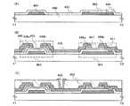
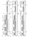
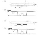
駆動回路のインバータ回路の断面構造を図1(A)に示す。なお、図1に示す第1薄膜ト
ランジスタ430、第2薄膜トランジスタ431は、逆スタガ型薄膜トランジスタであり
、酸化物半導体層上にソース領域またはドレイン領域を介して配線が設けられている薄膜
トランジスタの例である。A cross-sectional structure of the inverter circuit of the driver circuit is illustrated in FIG. Note that each of the first
図1(A)において、基板400上に第1ゲート電極401及び第2ゲート電極402が
形成される。第1ゲート電極401及び第2ゲート電極402上には、ゲート絶縁層40
3が形成される。また、第1ゲート電極401と重なる位置に、ゲート絶縁層403に接
する第1酸化物半導体層405が形成され、第2ゲート電極402と重なる位置に、ゲー
ト絶縁層403に接する第2酸化物半導体層407とが形成される。第1酸化物半導体層
405上には第1配線409、及び第2配線410が形成される。また、第1酸化物半導
体層405と、第1配線409、第2配線410の間に、ソース領域またはドレイン領域
として機能するn+層406a、406bが形成される。また、第2酸化物半導体層40
7と、第2配線410、第3配線411の間に、ソース領域またはドレイン領域として機
能するn+層408a、408bが形成される。また、第2配線410は、ゲート絶縁層
403に形成されたコンタクトホール404を介して、第2ゲート電極402と直接接続
する。また、第2酸化物半導体層407上には、第2配線410及び第3配線411が形
成される。また、第1酸化物半導体層405及び第2酸化物半導体層407に接する有機
絶縁層452が形成される。第1酸化物半導体層405及び第2酸化物半導体層407、
第1配線409〜第3配線411、及びゲート絶縁層403上に、組成物を塗布し、焼成
することで、第1酸化物半導体層405及び第2酸化物半導体層407に接する有機絶縁
層452を形成することができるため、電気特性の信頼性の高い薄膜トランジスタを作製
することができる。In FIG. 1A, a
3 is formed. In addition, a first
7, n+ layers 408 a and 408 b functioning as a source region or a drain region are formed between the
An organic insulating
基板400としては、透光性を有する基板を用いることが好ましく、透光性を有する基板
としては、コーニング社の7059ガラスや1737ガラスなどに代表されるバリウムホ
ウケイ酸ガラスやアルミノホウケイ酸ガラスなどのガラス基板を用いることができる。As the
第1ゲート電極401及び第2ゲート電極402の材料は、アルミニウム、銅、モリブデ
ン、タングステンから選ばれた元素、またはから選ばれた元素、または上述した元素と、
チタン、タンタル、タングステン、モリブデン、クロム、ネオジム、スカンジウム等とを
有する合金、または上述した元素の窒化物を用いた単層または積層構造で形成する。The material of the
It is formed with a single layer or a stacked structure using an alloy containing titanium, tantalum, tungsten, molybdenum, chromium, neodymium, scandium, or the like, or a nitride of the above element.
例えば、第1ゲート電極401及び第2ゲート電極402の2層の積層構造としては、ア
ルミニウム層上にモリブデン層が積層された構造、または銅層上にモリブデン層を積層し
た構造、または銅層上に窒化チタン層若しくは窒化タンタル層を積層した積層構造、窒化
チタン層とモリブデン層とを積層した構造とすることが好ましい。3層の積層構造として
は、タングステン層または窒化タングステン層と、アルミニウムとシリコンの合金または
アルミニウムとチタンの合金と、窒化チタン層またはチタン層とを積層した構造とするこ
とが好ましい。For example, the two-layer structure of the
ゲート絶縁層403としては、酸化シリコン層、窒化シリコン層、酸化窒化シリコン層ま
たは窒化酸化シリコン層を単層で、または積層して形成することができる。ゲート絶縁層
403を積層構造とする場合は、基板400上に窒化シリコン層または窒化酸化シリコン
層を形成し、その上に酸化シリコン層または酸化窒化シリコン層を形成する構造とするこ
とができる。The
また、第1ゲート電極401及び第2ゲート電極402を覆うゲート絶縁層403上には
、第1酸化物半導体層405と、第2酸化物半導体層407とを設ける。A first
第1酸化物半導体層405、第2酸化物半導体層407は、InMO3(ZnO)m(m
>0)で表記される層を形成する。なお、Mは、Ga、Fe、Ni、Mn及びCoから選
ばれた一の金属元素又は複数の金属元素を示す。例えばMとして、Gaの場合があること
の他、GaとNi又はGaとFeなど、Ga以外の上記金属元素が含まれる場合がある。
また、上記酸化物半導体において、Mとして含まれる金属元素の他に、不純物元素として
Fe、Niその他の遷移金属元素、又は該遷移金属の酸化物が含まれているものがある。
本明細書においてはこの薄膜をIn−Ga−Zn−O系非単結晶膜とも呼ぶ。また、第1
酸化物半導体層405、第2酸化物半導体層407の可動イオン、代表的にはナトリウム
の濃度は、5×10¹⁸/cm3以下、更には1×1018/cm3以下であると、薄膜
トランジスタの電気特性が変化することを抑制することができるため好ましい。The first
> 0) is formed. Note that M represents one metal element or a plurality of metal elements selected from Ga, Fe, Ni, Mn, and Co. For example, M may be Ga, and may contain the above metal elements other than Ga, such as Ga and Ni or Ga and Fe.
In addition to the metal element contained as M, some of the above oxide semiconductors contain Fe, Ni, other transition metal elements, or oxides of the transition metal as impurity elements.
In this specification, this thin film is also referred to as an In—Ga—Zn—O-based non-single-crystal film. The first
The concentration of mobile ions in the
本実施の形態では、ソース領域またはドレイン領域として機能するn+層406a、40
6b、408a、408bは、In−Ga−Zn−O系非単結晶層であり、第1酸化物半
導体層405、第2酸化物半導体層407の形成条件とは異なる形成条件で形成される、
より低抵抗な酸化物半導体層である。例えば、n+層406a、406b、408a、4
08bは、n型の導電型を有し、活性化エネルギー(ΔE)が0.01eV以上0.1e
V以下である。なお、本実施の形態では、n+層406a、406b、408a、408
bは、In−Ga−Zn−O系非単結晶層であり、少なくともアモルファス成分を含んで
いるものとする。n+層406a、406b、408a、408bは非晶質構造の中に結
晶粒(ナノクリスタル)を含む場合がある。このn+層406a、406b、408a、
408b中の結晶粒(ナノクリスタル)は直径1nm〜10nm、代表的には2nm〜4
nm程度である。In this embodiment, n+ layers 406a and 40 function as source regions or drain regions.
6b, 408a, and 408b are In—Ga—Zn—O-based non-single-crystal layers, which are formed under formation conditions different from the formation conditions of the first
It is a lower resistance oxide semiconductor layer. For example, n+ layers 406a, 406b, 408a, 4
08b has n-type conductivity, and its activation energy (ΔE) is 0.01 eV or more and 0.1 e.
V or less. Note that in this embodiment mode, the n+ layers 406a, 406b, 408a, 408
b is an In—Ga—Zn—O-based non-single-crystal layer, and includes at least an amorphous component. The n+ layers 406a, 406b, 408a, and 408b may include crystal grains (nanocrystals) in an amorphous structure. This n+ layer 406a, 406b, 408a,
The crystal grains (nanocrystals) in 408b have a diameter of 1 nm to 10 nm, typically 2 nm to 4 nm.
It is about nm.
n+層406a、406b、408a、408bを設けることにより、金属層である第1
配線409、第2配線410、第3配線411と、第1酸化物半導体層405、第2酸化
物半導体層407との間を良好な接合としてショットキー接合に比べて熱的にも安定動作
を有せしめる。また、チャネルのキャリアを供給する(ソース側)、またはチャネルのキ
ャリアを安定して吸収する(ドレイン側)、または抵抗成分を配線との界面に作らないた
めにも積極的にn+層を設けると効果的である。また低抵抗化により、高いドレイン電圧
でも良好な移動度を保持することができる。By providing the n+ layers 406a, 406b, 408a, and 408b, a first metal layer is formed.
As a good junction between the
第1配線409〜第3配線411の材料としては、アルミニウム、クロム、タンタル、チ
タン、モリブデン、タングステンから選ばれた元素、上述した元素を主成分とする合金、
または上述した元素を組み合わせた合金等がある。また、第1配線409〜第3配線41
1は、シリコンを含むアルミニウム層の単層構造や、チタン層の単層構造としてもよい。
また、第1配線409〜第3配線411は、2層構造としてもよく、アルミニウム層上に
チタン層を積層してもよい。As materials of the
Alternatively, there are alloys that combine the above-described elements. Also, the
1 may be a single layer structure of an aluminum layer containing silicon or a single layer structure of a titanium layer.
The
また、後の工程で、200℃〜600℃の熱処理を行う場合には、第1配線409〜第3
配線411に、当該熱処理に耐える耐熱性を持たせることが好ましい。アルミニウム単体
では耐熱性が劣り、また腐蝕しやすい等の問題点があるので、耐熱性導電性材料と組み合
わせて形成する。アルミニウムと組み合わせる耐熱性導電性材料としては、チタン、タン
タル、タングステン、モリブデン、クロム、ネオジム、スカンジウムから選ばれた元素、
上述した元素を主成分とする合金、上述した元素を複数組み合わせた合金、または上述し
た元素の窒化物で形成する。Further, when heat treatment at 200 ° C. to 600 ° C. is performed in a later process, the
It is preferable that the
An alloy containing the above-described element as a main component, an alloy combining a plurality of the above-described elements, or a nitride of the above-described element is used.
第1薄膜トランジスタ430は、第1ゲート電極401と、ゲート絶縁層403を介して
第1ゲート電極401と重なる第1酸化物半導体層405とを有し、第1配線409は、
接地電位の電源線(接地電源線)である。この接地電位の電源線は、負の電圧VDLが印
加される電源線(負電源線)としてもよい。The first
This is a ground potential power line (ground power line). The power supply line having the ground potential may be a power supply line (negative power supply line) to which a negative voltage VDL is applied.
また、第2薄膜トランジスタ431は、第2ゲート電極402と、ゲート絶縁層403を
介して第2ゲート電極402と重なる第2酸化物半導体層407とを有し、第3配線41
1は、正の電圧VDDが印加される電源線(正電源線)である。The second
図1(A)に示すように、第1酸化物半導体層405と第2酸化物半導体層407の両方
に電気的に接続する第2配線410は、ゲート絶縁層403に形成されたコンタクトホー
ル404を介して第2薄膜トランジスタ431の第2ゲート電極402と直接接続する。
直接接続させることにより、良好なコンタクトを得ることができ、接触抵抗を低減するこ
とができる。第2ゲート電極402と第2配線410を他の導電層、例えば透明導電層を
介して接続する場合に比べて、コンタクトホールの数の低減、コンタクトホールの数の低
減による占有面積の縮小を図ることができる。As shown in FIG. 1A, the
By direct connection, good contact can be obtained and contact resistance can be reduced. Compared to the case where the
有機絶縁層452は、組成物を塗布し焼成して形成することで、第1酸化物半導体層40
5及び第2酸化物半導体層407にダメージを与えず形成することができる。有機絶縁層
452として用いることが可能な有機材料としては、エポキシ樹脂、ポリイミド、アクリ
ル樹脂、ポリアクリロニトリル、ポリアミド、シリコーン樹脂、ポリエステル、シロキサ
ンポリマー、フッ素含有ポリマー、低誘電率材料(low−k材料)、PSG(リンガラ
ス)、BPSG(リンボロンガラス)等がある。The organic insulating
5 and the second
また、有機絶縁層452として、可視光の波長範囲のうち、任意の波長範囲の光を優先的
に透過させる機能を持たせてもよい。赤色波長範囲の光、青色波長範囲の光、及び緑色波
長範囲の光、それぞれを優先的に透過させる有機絶縁層を組み合わせて、カラーフィルタ
として機能させてもよい。しかしながら、着色層の組み合わせに関しては、これに限られ
ない。The organic insulating
本実施の形態では、第1酸化物半導体層405及び第2酸化物半導体層407に接して、
塗布法により形成される有機絶縁層452を形成するため、薄膜トランジスタの電気特性
の信頼性を向上させることができる。In this embodiment, in contact with the first
Since the organic insulating
また、駆動回路のインバータ回路の上面図を図1(C)に示す。図1(C)において、鎖
線Z1−Z2で切断した断面が図1(A)に相当する。A top view of the inverter circuit of the driver circuit is shown in FIG. In FIG. 1C, a cross section taken along the chain line Z1-Z2 corresponds to FIG.
なお、表示装置において、画素部を駆動するための駆動回路は、インバータ回路、容量、
抵抗などを用いて構成する。2つのnチャネル型薄膜トランジスタを組み合わせてインバ
ータ回路を形成する場合、エンハンスメント型トランジスタとデプレッション型トランジ
スタとを組み合わせて形成する場合(以下、EDMOS回路という)と、エンハンスメン
ト型薄膜トランジスタ同士で形成する場合(以下、EEMOS回路という)がある。なお
、nチャネル型薄膜トランジスタのしきい値電圧が正の場合は、エンハンスメント型トラ
ンジスタと定義し、nチャネル型薄膜トランジスタのしきい値電圧がゼロまたは負の場合
は、デプレッション型トランジスタと定義し、本明細書を通してこの定義に従うものとす
る。Note that in the display device, a driver circuit for driving the pixel portion includes an inverter circuit, a capacitor,
It is configured using resistors. When an inverter circuit is formed by combining two n-channel thin film transistors, an enhancement type transistor and a depletion type transistor are combined (hereinafter referred to as an EDMOS circuit), or an enhancement type thin film transistor (hereinafter referred to as an enhancement type thin film transistor). EEMOS circuit). Note that when the threshold voltage of the n-channel thin film transistor is positive, it is defined as an enhancement type transistor, and when the threshold voltage of the n-channel thin film transistor is zero or negative, it is defined as a depletion type transistor. This definition shall be followed throughout the document.
画素部と駆動回路は、同一基板上に形成し、画素部においては、マトリクス状に配置した
エンハンスメント型トランジスタを用いて画素電極への電圧印加のオン・オフを切り替え
る。この画素部に配置するエンハンスメント型トランジスタは、酸化物半導体を用いてお
り、その電気特性は、ゲート電圧±20Vにおいて、オン・オフ比が109以上であるた
め、リーク電流が少なく、低消費電力駆動を実現することができる。The pixel portion and the driver circuit are formed over the same substrate, and in the pixel portion, on / off of voltage application to the pixel electrode is switched using enhancement type transistors arranged in a matrix. The enhancement-type transistor disposed in this pixel portion uses an oxide semiconductor, and its electrical characteristics are such that an on / off ratio is 109 or more at a gate voltage of ± 20 V, so that there is little leakage current and low power consumption. Driving can be realized.
EDMOS回路の等価回路を図1(B)に示す。図1(A)及び図1(C)示す回路接続
は、図1(B)に相当し、第1薄膜トランジスタ430をエンハンスメント型のnチャネ
ル型トランジスタとし、第2薄膜トランジスタ431をデプレッション型のnチャネル型
トランジスタとする例である。An equivalent circuit of the EDMOS circuit is shown in FIG. 1A and 1C corresponds to FIG. 1B. The first
同一基板上にエンハンスメント型のnチャネル型トランジスタとデプレッション型のnチ
ャネル型トランジスタとを作製する方法は、例えば、第1酸化物半導体層405と第2酸
化物半導体層407とを異なる材料や異なる形成条件を用いて作製する。また、酸化物半
導体層の上下にゲート電極を設けてしきい値制御を行い、一方のTFTがノーマリーオン
となるようにゲート電極に電圧をかけ、もう一方のTFTがノーマリーオフとなるように
してEDMOS回路を構成してもよい。As a method for manufacturing an enhancement type n-channel transistor and a depletion type n-channel transistor over the same substrate, for example, the first
本実施の形態で示す薄膜トランジスタは、酸化物半導体層上に有機絶縁層が形成されるた
め、薄膜トランジスタの電気特性の信頼性を高めることができる。In the thin film transistor described in this embodiment, an organic insulating layer is formed over an oxide semiconductor layer; thus, reliability of electric characteristics of the thin film transistor can be improved.
(実施の形態2)
実施の形態1は、EDMOS回路の例を示したが、本実施の形態では、EEMOS回路の
等価回路を図2(A)に示す。また、EEMOSの上面図を図2(B)に示す。また、図
2に示すEEMOS回路の作製工程を図3に示す。図2(A)の等価回路においては、ど
ちらもエンハンスメント型のnチャネル型トランジスタとする組み合わせとする。(Embodiment 2)
Although
エンハンスメント型のnチャネル型トランジスタで作製できる図2(A)のEEMOS回
路を駆動回路に用いることで、画素部に用いるトランジスタと同様に、駆動回路において
も、エンハンスメント型のnチャネル型トランジスタを作製するため、作製工程が増大せ
ず、好ましいと言える。By using the EEMOS circuit in FIG. 2A which can be manufactured using an enhancement type n-channel transistor for a driver circuit, an enhancement type n-channel transistor is manufactured in the driver circuit as well as the transistor used for the pixel portion. Therefore, it can be said that the manufacturing process does not increase and is preferable.
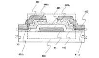
なお、図2に示す第1薄膜トランジスタ460、第2薄膜トランジスタ461は、逆スタ
ガ型薄膜トランジスタであり、酸化物半導体層上にソース領域またはドレイン領域を介し
て配線が設けられている薄膜トランジスタの例である。Note that each of the first
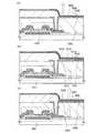
また、図2(B)中の鎖線Y1−Y2で切断した断面が、図3(C)に相当する。A cross section taken along chain line Y1-Y2 in FIG. 2B corresponds to FIG.
基板440上に、スパッタリング法により第1導電層を形成する。次に、第1フォトマス
クを用いたフォトリソグラフィ工程により形成したレジストマスクを用いて、選択的に第
1導電層のエッチングを行い、第1ゲート電極441及び第2ゲート電極442を形成す
る。この後、レジストマスクを除去する。A first conductive layer is formed over the
次に、第1ゲート電極401及び第2ゲート電極442を覆うゲート絶縁層443をプラ
ズマCVD法またはスパッタリング法を用いて形成する。ゲート絶縁層443は、CVD
法またはスパッタリング法等を用い、実施の形態1に列挙した材料を用いて形成すること
ができる。また、ゲート絶縁層443として、有機シランガスを用いたCVD法により酸
化シリコン層を形成することも可能である。有機シランガスとしては、珪酸エチル(TE
OS:化学式Si(OC2H5)4)、テトラメチルシラン(TMS:化学式Si(CH
3)4)、テトラメチルシクロテトラシロキサン(TMCTS)、オクタメチルシクロテ
トラシロキサン(OMCTS)、ヘキサメチルジシラザン(HMDS)、トリエトキシシ
ラン(SiH(OC2H5)3)、トリスジメチルアミノシラン(SiH(N(CH3)
2)3)等のシリコン含有化合物を用いることができる。Next, a
A method, a sputtering method, or the like can be used to form the material listed in
OS: chemical formula Si (OC2 H5 )4 ), tetramethylsilane (TMS: chemical formula Si (CH
3)4), tetramethylcyclotetrasiloxane (TMCTS), octamethylcyclotetrasiloxane (OMCTS), hexamethyldisilazane (HMDS), triethoxysilane(SiH(OC 2 H5) 3), trisdimethylaminosilane (SiH (N (CH3 )
A silicon-containing compound such as2 )3 ) can be used.
次いで、第2フォトマスクを用いたフォトリソグラフィ工程により形成したレジストマス
クを用いて、ゲート絶縁層443を選択的にエッチングして第2ゲート電極442に達す
るコンタクトホール444を形成する。この後、レジストマスクを除去する。ここまでの
段階での断面図が図3(A)に相当する。Next, the
次に、酸化物半導体層をスパッタリング法により形成し、さらにその上にn+層を形成す
る。なお、酸化物半導体層をスパッタリング法により形成する前に、アルゴンガスを導入
してプラズマを発生させる逆スパッタリングを行い、ゲート絶縁層443の表面及びコン
タクトホール444の底面に付着しているゴミを除去することが好ましい。逆スパッタリ
ングとは、ターゲット側に電圧を印加せずに、アルゴン雰囲気下で基板側にRF電源を用
いて電圧を印加して基板にプラズマを形成して表面を改質する方法である。なお、アルゴ
ン雰囲気に代えて窒素、ヘリウムなどを用いてもよい。また、アルゴン雰囲気に酸素、水
素、N2Oなどを加えた雰囲気で行ってもよい。また、アルゴン雰囲気にCl2、CF4
などを加えた雰囲気で行ってもよい。なお、逆スパッタリングを行うと、ゲート絶縁層4
03の表面が2〜10nm、好ましくは2〜10nm程度削られる。Next, an oxide semiconductor layer is formed by a sputtering method, and an n+ layer is further formed thereover. Note that before the oxide semiconductor layer is formed by a sputtering method, reverse sputtering that generates plasma by introducing argon gas is performed, so that dust attached to the surface of the
You may carry out in the atmosphere which added etc. When reverse sputtering is performed, the gate insulating layer 4
The surface of 03 is scraped by about 2 to 10 nm, preferably about 2 to 10 nm.
スパッタリング法にはスパッタリング用電源に高周波電源を用いるRFスパッタリング法
と、DCスパッタリング法があり、さらにパルス的にバイアスを与えるパルスDCスパッ
タリング法もある。RFスパッタリング法は主に絶縁層を形成する場合に用いられ、DC
スパッタリング法は主に金属層を形成する場合に用いられる。As the sputtering method, there are an RF sputtering method using a high-frequency power source as a sputtering power source and a DC sputtering method, and a pulse DC sputtering method for applying a bias in a pulsed manner. The RF sputtering method is mainly used when an insulating layer is formed.
The sputtering method is mainly used when a metal layer is formed.
また、材料の異なるターゲットを複数設置できる多元スパッタリング装置もある。多元ス
パッタリング装置は、同一チャンバーで異なる材料層を積層することも、同一チャンバー
で複数種類の材料を同時に放電させて形成することもできる。There is also a multi-source sputtering apparatus in which a plurality of targets of different materials can be installed. The multi-source sputtering apparatus can be formed by stacking different material layers in the same chamber or by simultaneously discharging a plurality of types of materials in the same chamber.
また、チャンバー内部に磁石機構を備えたマグネトロンスパッタリング法を用いるスパッ
タリング装置や、グロー放電を使わずマイクロ波を用いて発生させたプラズマを用いるE
CRスパッタリング法を用いるスパッタリング装置がある。Also, a sputtering apparatus using a magnetron sputtering method having a magnet mechanism inside the chamber, or an E using plasma generated using microwaves without using glow discharge.
There is a sputtering apparatus using a CR sputtering method.
また、形成方法として、成膜中にターゲット物質とスパッタリングガス成分とを化学反応
させてそれらの化合物薄膜を形成するリアクティブスパッタリング法や、成膜中に基板に
も電圧をかけるバイアススパッタリング法もある。As a forming method, there are a reactive sputtering method in which a target material and a sputtering gas component are chemically reacted during film formation to form a compound thin film thereof, and a bias sputtering method in which a voltage is applied to the substrate during film formation. .
本明細書のスパッタリングにおいては、上記したスパッタリング装置及びスパッタリング
方法を適宜用いることができる。In the sputtering of this specification, the above-described sputtering apparatus and sputtering method can be used as appropriate.
次いで、第3フォトマスクを用いて選択的に、酸化物半導体層及びn+層のエッチングを
行う。この後、レジストマスクを除去する。Next, the oxide semiconductor layer and the n+ layer are selectively etched using a third photomask. Thereafter, the resist mask is removed.
次に、スパッタリング法により第2導電層を形成する。次に、第4フォトマスクを用いた
フォトリソグラフィ工程により形成したレジストマスクを用いて選択的に第2導電層のエ
ッチングを行い、第1配線449、第2配線450、及び第3配線451を形成する。第
3配線451は、コンタクトホール444を介して第2ゲート電極442と直接接する。Next, a second conductive layer is formed by a sputtering method. Next, the second conductive layer is selectively etched using a resist mask formed by a photolithography process using a fourth photomask to form a
なお、第2導電層をスパッタリング法により形成する前に、アルゴンガスを導入してプラ
ズマを発生させる逆スパッタリングを行い、ゲート絶縁層443の表面、n+層の表面、
及びコンタクトホール444の底面に付着しているゴミを除去することが好ましい。なお
、アルゴン雰囲気に代えて窒素、ヘリウムなどを用いてもよい。また、アルゴン雰囲気に
酸素、水素、N2Oなどを加えた雰囲気で行ってもよい。また、アルゴン雰囲気にCl2
、CF4などを加えた雰囲気で行ってもよい。Note that before the second conductive layer is formed by a sputtering method, reverse sputtering in which an argon gas is introduced to generate plasma is performed, and the surface of the
It is preferable to remove dust attached to the bottom surface of the
, CF4 or the like.
なお、第2導電層のエッチングの際に、さらに、n+層及び酸化物半導体層の一部をエッ
チングして、n+層446a、446b、448a、448b、第1酸化物半導体層44
5、第2酸化物半導体層447を形成する。このエッチングで第1ゲート電極及び第2ゲ
ート電極と重なる部分の第1酸化物半導体層445、第2酸化物半導体層447の厚さは
薄くなる。この後、レジストマスクを除去する。このエッチングが終了した段階で第1薄
膜トランジスタ460と第2薄膜トランジスタ461が完成する。ここまでの段階での断
面図が図3(B)に相当する。Note that when the second conductive layer is etched, the n+ layer and a part of the oxide semiconductor layer are further etched to form the n+ layers 446a, 446b, 448a, 448b, and the first oxide semiconductor layer 44.
5. A second
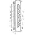
ここで、第1薄膜トランジスタ460の拡大図を図43に示す。第2導電層をスパッタリ
ング法により形成する前に逆スパッタリングを行うと、ゲート絶縁層443の露出部が2
〜10nm、好ましくは2〜10nm程度削られるため、図43に示すように、ゲート絶
縁層443と、後に形成される第1配線449及び第2配線450が接する領域において
、ゲート絶縁層443に凹部471a、471bが形成される。Here, an enlarged view of the first
Since the thickness is reduced to about 10 nm, preferably about 2 to 10 nm, a recess is formed in the
また、第2導電層のエッチングを行い、第1配線449、第2配線450、及び第3配線
451を形成した後、逆スパッタリングすることで、図3(B)に示すように、第1配線
449、第2配線450、及び第3配線451の端部が湾曲する。Further, after the second conductive layer is etched to form the
次に、大気雰囲気下または窒素雰囲気下で200℃〜600℃の加熱処理を行う。この熱
処理によりIn−Ga−Zn−O系非単結晶層の原子レベルの再配列が行われる。この熱
処理によりキャリアの移動を阻害する歪が解放されるため、ここでの熱処理(光アニール
も含む)は重要である。なお、この加熱処理を行うタイミングは限定されず、酸化物半導
体層445、447の形成後であれば、いつ行ってもよい。Next, heat treatment is performed at 200 ° C. to 600 ° C. in an air atmosphere or a nitrogen atmosphere. By this heat treatment, rearrangement at the atomic level of the In—Ga—Zn—O-based non-single-crystal layer is performed. Since heat treatment releases strain that hinders carrier movement, heat treatment here (including optical annealing) is important. Note that the timing of performing this heat treatment is not limited and may be any time after the oxide semiconductor layers 445 and 447 are formed.
次に、有機絶縁層の材料である組成物を塗布し、大気雰囲気下または窒素雰囲気下で20
0℃〜600℃の加熱処理を行って、有機絶縁層452を形成する。有機絶縁層452は
、実施の形態1に示す材料を適宜用いることができる。図3(C)においては、非感光性
樹脂を用いて有機絶縁層452を形成した形態を示したため、コンタクトホールが形成さ
れる領域の断面において、有機絶縁層452の端部が角張っている。しかしながら、感光
性樹脂を用いて有機絶縁層452を形成すると、図44に示すように、コンタクトホール
が形成される領域の断面において、有機絶縁層452の端部は湾曲している。この結果、
後に形成される接続配線453や画素電極の被覆率が向上する。Next, a composition which is a material of the organic insulating layer is applied, and 20% in an air atmosphere or a nitrogen atmosphere.
A heat treatment at 0 ° C. to 600 ° C. is performed to form the organic insulating
The coverage of
また、組成物を塗布する代わりに、その材料に応じて、ディップ、スプレー塗布、インク
ジェット法、印刷法、ドクターナイフ、ロールコーター、カーテンコーター、ナイフコー
ター等を用いることができる。Further, instead of applying the composition, dip, spray coating, ink jet method, printing method, doctor knife, roll coater, curtain coater, knife coater or the like can be used depending on the material.
なお、酸化物半導体層445、447を形成した後の加熱処理をせず、有機絶縁層の材料
である組成物の加熱処理時に、酸化物半導体層445、447の加熱処理を兼ねてもよい
。Note that heat treatment after the oxide semiconductor layers 445 and 447 are formed may be combined with heat treatment of the oxide semiconductor layers 445 and 447 at the time of heat treatment of the composition that is a material of the organic insulating layer.
有機絶縁層452は、200nm〜5μm、好ましくは300nm〜1μmで形成する。The organic insulating
次に、第3導電層を形成する。次に、第5フォトマスクを用いたフォトリソグラフィ工程
により形成したレジストマスクを用いて第3導電層を選択的にエッチングして、第2配線
410と電気的に接続する接続配線453を形成する。ここまでの段階での断面図が図3
(C)に相当する。Next, a third conductive layer is formed. Next, the third conductive layer is selectively etched using a resist mask formed by a photolithography process using a fifth photomask, so that connection wirings 453 that are electrically connected to the
Corresponds to (C).
なお、レジストマスクをウェットエッチングで除去した後、大気雰囲気下または窒素雰囲
気下で200℃〜600℃の加熱処理を行ってもよい。Note that after the resist mask is removed by wet etching, heat treatment at 200 ° C. to 600 ° C. may be performed in an air atmosphere or a nitrogen atmosphere.
発光素子を用いた発光表示装置においては、画素部に複数の薄膜トランジスタを有し、画
素部においても、ある一つの薄膜トランジスタのゲート電極と他のトランジスタのソース
配線、或いはドレイン配線を直接接続させるためのコンタクトホールを有している。この
コンタクトホールは、第2フォトマスクを用いてゲート絶縁層にコンタクトホールを形成
する際に同じマスクを用いて形成することができる。In a light-emitting display device using a light-emitting element, a pixel portion includes a plurality of thin film transistors, and in the pixel portion, a gate electrode of one thin film transistor and a source wiring or a drain wiring of another transistor are directly connected. Has a contact hole. This contact hole can be formed using the same mask when the contact hole is formed in the gate insulating layer using the second photomask.
また、液晶表示装置や電子ペーパーにおいては、FPCなどの外部端子と接続するための
端子部において、ゲート配線に達するコンタクトホールを形成する際、第2フォトマスク
を用いてゲート絶縁層にコンタクトホールを形成する際に同じマスクを用いて形成するこ
とができる。In a liquid crystal display device or electronic paper, when a contact hole reaching a gate wiring is formed in a terminal portion for connecting to an external terminal such as an FPC, a contact hole is formed in the gate insulating layer using a second photomask. When forming, the same mask can be used.
なお、上述した工程順序は一例であって特に限定されない。例えば、フォトマスク数が1
枚増えるが、第2導電層をエッチングするフォトマスクと、n+層及び酸化物半導体層の
一部をエッチングするフォトマスクを別々に用いてエッチングを行ってもよい。In addition, the process sequence mentioned above is an example, and is not specifically limited. For example, the number of photomasks is 1
Although the number of the layers increases, the photomask for etching the second conductive layer and the photomask for etching part of the n+ layer and the oxide semiconductor layer may be separately used for etching.
以上の工程により、酸化物半導体層に接する有機絶縁層を形成することで、電気特性の信
頼性の高い薄膜トランジスタを作製することができる。By forming the organic insulating layer in contact with the oxide semiconductor layer through the above steps, a thin film transistor with high electrical characteristics can be manufactured.
(実施の形態3)
本実施の形態では、インバータ回路の作製において、実施の形態2とは異なる作製工程の
例を図4(A)、図4(B)、及び図4(C)を用いて説明する。(Embodiment 3)
In this embodiment, an example of a manufacturing process which is different from that in
基板440上に、スパッタリング法により第1導電層を形成する。次に、第1フォトマス
クを用いたフォトリソグラフィ工程により形成したレジストマスクを用いて、選択的に第
1導電層のエッチングを行い、第1ゲート電極441及び第2ゲート電極442を形成す
る。この後、レジストマスクを除去する。A first conductive layer is formed over the
次に、第1ゲート電極441及び第2ゲート電極442を覆うゲート絶縁層443をプラ
ズマCVD法またはスパッタリング法を用いて形成する。Next, a
次に、酸化物半導体層をスパッタリング法により形成し、さらにその上にn+層を形成す
る。Next, an oxide semiconductor layer is formed by a sputtering method, and an n+ layer is further formed thereover.
次いで、第2フォトマスクを用いたフォトリソグラフィ工程により形成したレジストマス
クを用いて、選択的に、酸化物半導体層及びn+層のエッチングを行う。こうして、第1
ゲート電極441とゲート絶縁層443を介して重なる酸化物半導体層454、及びn+
層455が形成され、第2ゲート電極442とゲート絶縁層443を介して重なる酸化物
半導体層456、n+層457が形成される。ここまでの段階での断面図が図4(A)に
相当する。Next, the oxide semiconductor layer and the n+ layer are selectively etched using a resist mask formed by a photolithography process using a second photomask. Thus, the first
An
The
次いで、第3フォトマスクを用いフォトリソグラフィ工程により形成したレジストマスク
を用いて、ゲート絶縁層443を選択的にエッチングして第2ゲート電極442に達する
コンタクトホール444を形成する。この後、レジストマスクを除去する。ここまでの段
階での断面図が図4(B)に相当する。Next, the
次いで、スパッタリング法により第2導電層を形成し、第4フォトマスクを用いて選択的
に第2導電層のエッチングを行い、第1配線449、第2配線450、及び第3配線45
1を形成する。Next, a second conductive layer is formed by a sputtering method, and the second conductive layer is selectively etched using a fourth photomask, whereby the
1 is formed.
なお、第2導電層をスパッタリング法により形成する前に、アルゴンガスを導入してプラ
ズマを発生させる逆スパッタリングを行い、ゲート絶縁層443の表面、n+層455、
457の表面、及びコンタクトホール444の底面に付着しているゴミを除去することが
好ましい。なお、アルゴン雰囲気に代えて窒素、ヘリウムなどを用いてもよい。また、ア
ルゴン雰囲気に酸素、水素、N2Oなどを加えた雰囲気で行ってもよい。また、アルゴン
雰囲気にCl2、CF4などを加えた雰囲気で行ってもよい。Note that before the second conductive layer is formed by a sputtering method, reverse sputtering that generates plasma by introducing argon gas is performed, and the surface of the
It is preferable to remove dust attached to the surface of 457 and the bottom surface of the
本実施の形態の工程においては、コンタクトホール444を形成した後、他の層を形成す
ることなく第2導電層を形成することができるため、実施の形態2に比べてコンタクトホ
ールの底面が曝される工程数が少ないため、ゲート電極の材料の材料選択の自由度が広が
る。これは、実施の形態2においては、コンタクトホール444で露出しているゲート電
極面に接して酸化物半導体層が形成されるため、酸化物半導体層のエッチング工程でゲー
ト電極の材料がエッチングされないエッチング条件またはゲート電極の材料を選択する必
要があるためである。In the process of this embodiment mode, after the
なお、第2導電層のエッチングの際に、さらに、n+層及び酸化物半導体層の一部をエッ
チングして、n+層446a、446b、448a、448b、第1酸化物半導体層44
5、第2酸化物半導体層447を形成する。このエッチングで第1ゲート電極及び第2ゲ
ート電極と重なる部分の第1酸化物半導体層445、第2酸化物半導体層447の厚さは
薄くなる。この後、レジストマスクを除去する。このエッチングが終了した段階で第1薄
膜トランジスタ460と第2薄膜トランジスタ461が完成する。Note that when the second conductive layer is etched, the n+ layer and a part of the oxide semiconductor layer are further etched to form the n+ layers 446a, 446b, 448a, 448b, and the first oxide semiconductor layer 44.
5. A second
第1薄膜トランジスタ460は、第1ゲート電極441と、ゲート絶縁層443を介して
第1ゲート電極441と重なる第1酸化物半導体層445とを有し、第1配線449は、
接地電位の電源線(接地電源線)である。この接地電位の電源線は、負の電圧VDLが印
加される電源線(負電源線)としてもよい。The first
This is a ground potential power line (ground power line). The power supply line having the ground potential may be a power supply line (negative power supply line) to which a negative voltage VDL is applied.
また、第2薄膜トランジスタ461は、第2ゲート電極442と、ゲート絶縁層443を
介して第2ゲート電極442と重なる第2酸化物半導体層447とを有し、第3配線45
1は、正の電圧VDDが印加される電源線(正電源線)である。The second
また、第1酸化物半導体層445と第1配線449との間にはn+層446aを設け、第
1酸化物半導体層445と第2配線450との間にはn+層446bを設ける。また、第
2酸化物半導体層447と第2配線450との間にはn+層448aを設け、第2酸化物
半導体層447と第3配線451との間にはn+層448bを設ける。Further, the first
ここまでの段階での断面図が図4(C)に相当する。A cross-sectional view of the steps so far corresponds to FIG.
次に、大気雰囲気下または窒素雰囲気下で200℃〜600℃の加熱処理を行う。なお、
この加熱処理を行うタイミングは限定されず、酸化物半導体層の形成後であれば、いつ行
ってもよい。Next, heat treatment is performed at 200 ° C. to 600 ° C. in an air atmosphere or a nitrogen atmosphere. In addition,
The timing for performing the heat treatment is not limited, and may be any time after the oxide semiconductor layer is formed.
次に、有機絶縁層の材料である組成物を塗布し、大気雰囲気下または窒素雰囲気下で20
0℃〜600℃の加熱処理を行って、有機絶縁層452を形成する。有機絶縁層452は
、実施の形態1に示す材料を適宜用いることができる。なお、第1酸化物半導体層445
、第2酸化物半導体層447を形成した後の加熱処理をせず、有機絶縁層の材料である組
成物の加熱処理時に、酸化物半導体層445、447の加熱処理を兼ねてもよい。Next, a composition which is a material of the organic insulating layer is applied, and 20% in an air atmosphere or a nitrogen atmosphere.
A heat treatment at 0 ° C. to 600 ° C. is performed to form the organic insulating
The heat treatment after the formation of the second
次に、第5フォトマスクを用いたフォトリソグラフィ工程により形成したレジストマスク
を用いて、有機絶縁層452を選択的にエッチングしてコンタクトホールを形成する。こ
の後、レジストマスクを除去する。なお、有機絶縁層452が感光性樹脂で形成される場
合、有機絶縁層452上にレジストを塗布せず、第5フォトマスクを用いて有機絶縁層を
露光現像して、有機絶縁層452にコンタクトホールを形成することができる。Next, a contact hole is formed by selectively etching the organic insulating
次に、第3導電層を形成する。次に、第6フォトマスクを用いたフォトリソグラフィ工程
により形成したレジストマスクを用いて第3導電層を選択的にエッチングして、第2配線
450と電気的に接続する接続配線453を形成する。ここまでの段階での断面図が図4
(D)に相当する。Next, a third conductive layer is formed. Next, the third conductive layer is selectively etched using a resist mask formed by a photolithography process using a sixth photomask, so that connection wirings 453 that are electrically connected to the
Corresponds to (D).
なお、レジストマスクをウェットエッチングで除去した場合、大気雰囲気下または窒素雰
囲気下で200℃〜600℃の加熱処理を行ってもよい。Note that when the resist mask is removed by wet etching, heat treatment at 200 ° C. to 600 ° C. may be performed in an air atmosphere or a nitrogen atmosphere.
発光素子を用いた発光表示装置においては、画素部に複数の薄膜トランジスタを有し、画
素部においてもある薄膜トランジスタのゲート電極と他のトランジスタのソース配線、或
いはドレイン配線を直接接続させるためのコンタクトホールを有している。このコンタク
ト部は、第3フォトマスクを用いてゲート絶縁層にコンタクトホールを形成する際に同じ
マスクを用いて形成することができる。In a light-emitting display device using a light-emitting element, a pixel portion includes a plurality of thin film transistors, and a contact hole for directly connecting a gate electrode of a thin film transistor in the pixel portion to a source wiring or a drain wiring of another transistor is provided. Have. This contact portion can be formed using the same mask when the contact hole is formed in the gate insulating layer using the third photomask.
また、液晶表示装置や電子ペーパーにおいては、FPCなどの外部端子と接続するための
端子部において、ゲート配線に達するコンタクトホールを形成する際、第3フォトマスク
を用いてゲート絶縁層にコンタクトホールを形成する際に同じマスクを用いて形成するこ
とができる。In a liquid crystal display device or electronic paper, when a contact hole reaching a gate wiring is formed in a terminal portion for connecting to an external terminal such as an FPC, a contact hole is formed in the gate insulating layer using a third photomask. When forming, the same mask can be used.
なお、上述した工程順序は一例であって特に限定されない。例えば、フォトマスク数が1
枚増えるが、第2導電層をエッチングするフォトマスクと、n+層及び酸化物半導体層の
一部をエッチングするフォトマスクを別々に用いてエッチングを行ってもよい。In addition, the process sequence mentioned above is an example, and is not specifically limited. For example, the number of photomasks is 1
Although the number of the layers increases, the photomask for etching the second conductive layer and the photomask for etching part of the n+ layer and the oxide semiconductor layer may be separately used for etching.
以上の工程により、酸化物半導体層に接する有機絶縁層を形成することで、電気特性の信
頼性の高い薄膜トランジスタを作製することができる。By forming the organic insulating layer in contact with the oxide semiconductor layer through the above steps, a thin film transistor with high electrical characteristics can be manufactured.
(実施の形態4)
本実施の形態では、実施の形態1または実施の形態2に示した駆動回路と同一基板上に形
成できる画素部の薄膜トランジスタ、及び端子部の作製工程について、図5乃至図12を
用いて説明する。(Embodiment 4)
In this embodiment, a manufacturing process of a thin film transistor in a pixel portion and a terminal portion that can be formed over the same substrate as the driver circuit described in
図5(A)において、基板100には、実施の形態1に示す基板400を適宜用いること
ができる。5A, the
次に、基板100全面に導電層を形成した後、第1フォトリソグラフィ工程を行って形成
したレジストマスクを用いたエッチングにより不要な部分を除去して、配線及び電極(ゲ
ート電極101を含むゲート配線、容量配線108、及び第1端子121)を形成する。
このとき少なくともゲート電極101の端部にテーパー形状が形成されるようにエッチン
グする。この後、レジストマスクを除去する。なお、この段階での上面図が図7に相当す
る。後に形成される酸化物半導体層、ソース電極層、ドレイン電極層、画素電極、コンタ
クトホールは破線で示されている。Next, after a conductive layer is formed over the entire surface of the
At this time, etching is performed so that at least an end portion of the
ゲート電極101を含むゲート配線と容量配線108、端子部の第1端子121は、実施
の形態1に示す第1ゲート電極401、第2ゲート電極402の材料を適宜用いて形成す
る。The gate wiring including the
次に、ゲート電極101上にゲート絶縁層102を全面に形成する。ゲート絶縁層102
は、実施の形態1に示すゲート絶縁層403の適宜用い、スパッタリング法などを用い、
厚さを50〜250nmとする。Next, a
The
The thickness is 50 to 250 nm.
なお、酸化物半導体層を形成する前に、アルゴンガスを導入してプラズマを発生させる逆
スパッタリングを行い、ゲート絶縁層の表面に付着しているゴミを除去することが好まし
い。なお、アルゴン雰囲気に代えて窒素、ヘリウムなどを用いてもよい。また、アルゴン
雰囲気に酸素、水素、N2Oなどを加えた雰囲気で行ってもよい。また、アルゴン雰囲気
にCl2、CF4などを加えた雰囲気で行ってもよい。Note that before the oxide semiconductor layer is formed, it is preferable to perform reverse sputtering in which an argon gas is introduced to generate plasma to remove dust attached to the surface of the gate insulating layer. Note that nitrogen, helium, or the like may be used instead of the argon atmosphere. Alternatively, an atmosphere in which oxygen, hydrogen, N2 O, or the like is added to an argon atmosphere may be used. Alternatively, an atmosphere in which Cl2 , CF4, or the like is added to an argon atmosphere may be used.
次に、ゲート絶縁層102上に、第1酸化物半導体層(本実施の形態では第1In−Ga
−Zn−O系非単結晶層)を形成する。プラズマ処理後、大気に曝すことなく第1In−
Ga−Zn−O系非単結晶層を形成することは、ゲート絶縁層と酸化物半導体層の界面に
ゴミや水分を付着させない点で有用である。Next, over the
-Zn-O-based non-single crystal layer). After the plasma treatment, the first In-
The formation of the Ga—Zn—O-based non-single-crystal layer is useful in that dust and moisture are not attached to the interface between the gate insulating layer and the oxide semiconductor layer.
ここでは、直径8インチのIn、Ga、及びZnを含む酸化物半導体ターゲット(In2
O3:Ga2O3:ZnO=1:1:1)を用いて、基板とターゲットの間との距離を1
70mm、圧力0.4Pa、直流(DC)電源0.5kW、アルゴンまたは酸素雰囲気下
で形成する。なお、パルス直流(DC)電源を用いると、ごみが軽減でき、膜厚分布も均
一となるために好ましい。第1In−Ga−Zn−O系非単結晶層の厚さは、5nm〜2
00nmとする。本実施の形態では第1In−Ga−Zn−O系非単結晶層の厚さを、1
00nmとする。Here, an oxide semiconductor target containing In, Ga, and Zn having an diameter of 8 inches (In2
O3 : Ga2 O3 : ZnO = 1: 1: 1), the distance between the substrate and the target is 1
It is formed in 70 mm, pressure 0.4 Pa, direct current (DC) power supply 0.5 kW, argon or oxygen atmosphere. Note that a pulse direct current (DC) power source is preferable because dust can be reduced and the film thickness can be uniform. The thickness of the first In—Ga—Zn—O-based non-single-crystal layer is 5 nm to 2 nm.
Set to 00 nm. In this embodiment, the thickness of the first In—Ga—Zn—O-based non-single-crystal layer is set to 1
Set to 00 nm.
次いで、大気に曝すことなく、第2酸化物半導体層(本実施の形態では第2In−Ga−
Zn−O系非単結晶層)をスパッタリング法で形成する。ここでは、In2O3:Ga2
O3:ZnO=1:1:1としたターゲットを用い、形成条件は、圧力を0.4Paとし
、電力を500Wとし、成膜温度を室温とし、アルゴンガス流量40sccmを導入して
、スパッタリングを行う。In2O3:Ga2O3:ZnO=1:1:1としたターゲッ
トを意図的に用いているにも関わらず、成膜直後で大きさ1nm〜10nmの結晶粒を含
むIn−Ga−Zn−O系非単結晶層が形成されることがある。なお、ターゲットの成分
比、成膜圧力(0.1Pa〜2.0Pa)、電力(250W〜3000W:8インチφ)
、温度(室温〜100℃)、反応性スパッタリングの形成条件などを適宜調節することで
結晶粒の有無や、結晶粒の密度や、直径サイズは、1nm〜10nmの範囲で調節されう
ると言える。第2In−Ga−Zn−O系非単結晶層の厚さは、5nm〜20nmとする
。勿論、層中に結晶粒が含まれる場合、含まれる結晶粒のサイズが厚さを超える大きさと
ならない。本実施の形態では第2In−Ga−Zn−O系非単結晶層の厚さは、5nmと
する。Next, the second oxide semiconductor layer (the second In—Ga— in this embodiment is not exposed to the atmosphere).
Zn—O-based non-single crystal layer) is formed by a sputtering method. Here, In2 O3 : Ga2
Using a target with O3 : ZnO = 1: 1: 1, the formation conditions were a pressure of 0.4 Pa, a power of 500 W, a film formation temperature of room temperature, an argon gas flow rate of 40 sccm, and sputtering. Do. In—Ga— containing crystal grains having a size of 1 nm to 10 nm immediately after film formation, despite the intentional use of a target of In2 O3 : Ga2 O3 : ZnO = 1: 1: 1. A Zn—O-based non-single crystal layer may be formed. In addition, target component ratio, film forming pressure (0.1 Pa to 2.0 Pa), power (250 W to 3000 W: 8 inches φ)
It can be said that the presence or absence of crystal grains, the density of crystal grains, and the diameter size can be adjusted in the range of 1 nm to 10 nm by appropriately adjusting the temperature (room temperature to 100 ° C.), the reactive sputtering formation conditions, and the like. The thickness of the second In—Ga—Zn—O-based non-single-crystal layer is 5 nm to 20 nm. Of course, when crystal grains are included in the layer, the size of the included crystal grains does not exceed the thickness. In this embodiment, the thickness of the second In—Ga—Zn—O-based non-single-crystal layer is 5 nm.
第1In−Ga−Zn−O系非単結晶層は、第2In−Ga−Zn−O系非単結晶層の形
成条件と異ならせる。例えば、第2In−Ga−Zn−O系非単結晶層の形成条件におけ
る酸素ガス流量とアルゴンガス流量の比よりも、第1In−Ga−Zn−O系非単結晶層
の形成条件における酸素ガス流量の占める比率が多い条件とする。具体的には、第2In
−Ga−Zn−O系非単結晶層の形成条件は、希ガス(アルゴン、またはヘリウムなど)
雰囲気下(または酸素ガス10%以下、アルゴンガス90%以上)とし、第1In−Ga
−Zn−O系非単結晶層の形成条件は、酸素雰囲気下(または酸素ガス流量とアルゴンガ
ス流量の比1:1)とする。The first In—Ga—Zn—O-based non-single-crystal layer is different from the formation conditions of the second In—Ga—Zn—O-based non-single-crystal layer. For example, the oxygen gas in the formation condition of the first In—Ga—Zn—O-based non-single-crystal layer is larger than the ratio of the oxygen gas flow rate to the argon gas flow rate in the formation condition of the second In—Ga—Zn—O-based non-single-crystal layer. The conditions are such that the ratio of flow rate is large. Specifically, the second In
The formation condition of the —Ga—Zn—O-based non-single-crystal layer is a rare gas (such as argon or helium).
Under an atmosphere (or oxygen gas 10% or less, argon gas 90% or more), the first In—Ga
The formation condition of the —Zn—O-based non-single-crystal layer is an oxygen atmosphere (or a ratio of an oxygen gas flow rate to an argon gas flow rate of 1: 1).
次に、第2フォトリソグラフィ工程を行ってレジストマスクを形成し、当該レジストマス
クを用いて、第1In−Ga−Zn−O系非単結晶層及び第2In−Ga−Zn−O系非
単結晶層をエッチングする。ここでは、エッチャントとしてITO07N(関東化学社製
)を用いたウェットエッチングにより、不要な部分を除去して第1In−Ga−Zn−O
系非単結晶層である酸化物半導体層109、第2In−Ga−Zn−O系非単結晶層であ
る酸化物半導体層111を形成する。なお、ここでのエッチングは、ウェットエッチング
に限定されずドライエッチングを用いてもよい。この段階での上面図を図5(B)に示し
た。なお、この段階での上面図が図8に相当する。後に形成されるソース電極、ドレイン
電極、画素電極、コンタクトホール等は破線で示されている。この後、レジストマスクを
除去する。Next, a second photolithography step is performed to form a resist mask, and the first In—Ga—Zn—O-based non-single crystal layer and the second In—Ga—Zn—O-based non-single crystal are formed using the resist mask. Etch the layer. Here, unnecessary portions are removed by wet etching using ITO07N (manufactured by Kanto Chemical Co., Inc.) as an etchant to remove the first In—Ga—Zn—O.
The
次いで、第3フォトリソグラフィ工程を行ってレジストマスクを形成し、当該レジストマ
スクを用いたエッチングにより、不要な部分を除去してゲート電極と同じ材料の配線や電
極に達するコンタクトホールを形成する。このコンタクトホールは後に形成する導電層と
直接接続するために設ける。例えば、駆動回路部において、ゲート電極とソース電極或い
はドレイン電極と直接接する薄膜トランジスタや、端子部のゲート配線と電気的に接続す
る端子を形成する場合にコンタクトホールを形成する。この後、レジストマスクを除去す
る。Next, a resist mask is formed by performing a third photolithography step, and unnecessary portions are removed by etching using the resist mask to form a contact hole reaching the wiring or electrode of the same material as the gate electrode. This contact hole is provided for direct connection to a conductive layer to be formed later. For example, a contact hole is formed when a thin film transistor in direct contact with a gate electrode and a source electrode or a drain electrode or a terminal electrically connected to a gate wiring in a terminal portion is formed in a driver circuit portion. Thereafter, the resist mask is removed.
次に、酸化物半導体層109及び酸化物半導体層111上に金属材料からなる導電層13
2を、スパッタリング法や真空蒸着法で形成する。この段階での断面図を図5(C)に示
す。Next, the conductive layer 13 made of a metal material over the
2 is formed by sputtering or vacuum deposition. A cross-sectional view at this stage is illustrated in FIG.
導電層132の材料としては、実施の形態1に示す第1配線409〜第3配線411の材
料を適宜用いることができる。As a material of the
次に、第4フォトリソグラフィ工程を行ってレジストマスク131を形成し、当該レジス
トマスクを用いたエッチングにより不要な部分を除去して、ソース電極またはドレイン電
極105a、105b、ソース領域またはドレイン領域として機能するn+層104a、
104b、及び接続電極120、第2端子122を形成する。この際のエッチング方法と
してウェットエッチングまたはドライエッチングを用いる。Next, a resist
104b, the
例えば導電層132としてアルミニウム層、またはアルミニウム合金層を用いる場合は、
燐酸と酢酸と硝酸を混ぜた溶液を用いたウェットエッチングを行うことができる。ここで
は、アンモニア過水(過酸化水素:アンモニア:水=5:2:2)を用いたウェットエッ
チングにより、チタン層で形成される導電層132をエッチングして、ソース電極または
ドレイン電極105a、105bを形成する。また、酸化物半導体層111をエッチング
して、n+層104a、104bを形成する。このエッチング工程において、酸化物半導
体層109の露出領域も一部エッチングされ、酸化物半導体層103となる。よってn+
層104a、104bの間の酸化物半導体層103のチャネル領域は、厚さの薄い領域と
なる。For example, when an aluminum layer or an aluminum alloy layer is used as the
Wet etching using a mixed solution of phosphoric acid, acetic acid and nitric acid can be performed. Here, the
A channel region of the
図6(A)においては、ソース電極またはドレイン電極105a、105b、n+層10
4a、104bのエッチングをアンモニア過水のエッチング材によって一度に行うため、
ソース電極またはドレイン電極105a、105b及、びn+層104a、104bの端
部は一致し、連続的な構造となっている。またウェットエッチングを用いるために、エッ
チングが等方的に行われ、ソース電極またはドレイン電極105a、105bの端部はレ
ジストマスク131より後退している。この後、レジストマスクを除去する。以上の工程
で酸化物半導体層103をチャネル形成領域とする薄膜トランジスタ170を作製するこ
とができる。この段階での断面図を図6(A)に示す。なお、この段階での上面図が図9
に相当する。後に形成される画素電極、コンタクトホール等は破線で示されている。In FIG. 6A, source or
In order to perform the etching of 4a and 104b at once with the etching agent of ammonia-water,
The end portions of the source or
It corresponds to. Pixel electrodes, contact holes, and the like that are formed later are indicated by broken lines.
さらに、露出している酸化物半導体層103のチャネル形成領域に、酸素ラジカル処理を
行ってもよい。酸素ラジカル処理を行うことにより薄膜トランジスタをノーマリーオフと
することができる。また、ラジカル処理を行うことにより、酸化物半導体層103のエッ
チングによるダメージを回復することができる。ラジカル処理はO2、N2O、好ましく
は酸素を含むN2、He、Ar雰囲気下で行うことが好ましい。また、上記雰囲気にCl
2、CF4を加えた雰囲気下で行ってもよい。なお、ラジカル処理は、無バイアスで行う
ことが好ましい。また、当該ラジカル処理により、ソース電極105a、ドレイン電極1
05b、接続電極120、及び第2端子122の端部が湾曲する。Further, oxygen radical treatment may be performed on the exposed channel formation region of the
2, CF4 and may be carried out in an atmosphere which was added. Note that the radical treatment is preferably performed without bias. Further, by the radical treatment, the
05b, the
なお、当該ラジカル処理を行わなかった場合は、図6(A)に示すように、ソース電極1
05a、ドレイン電極105b、接続電極120、及び第2端子122の端部は湾曲せず
、角張っている。When the radical treatment is not performed, as shown in FIG. 6A, the
The ends of 05a, the
また、この第4フォトリソグラフィ工程において、ソース電極またはドレイン電極105
a、105bと同じ材料である第2端子122を端子部に残す。なお、第2端子122は
ソース配線(ソース電極またはドレイン電極105a、105bを含むソース配線)と電
気的に接続されている。In the fourth photolithography step, the source electrode or the drain electrode 105
The
また、端子部において、接続電極120は、ゲート絶縁層に形成されたコンタクトホール
を介して端子部の第1端子121と直接接続される。なお、ここでは図示しないが、上述
した工程と同じ工程を経て駆動回路の薄膜トランジスタのソース配線あるいはドレイン配
線とゲート電極が直接接続される。In the terminal portion, the
次に、200℃〜600℃、代表的には300℃〜500℃の熱処理を行うことが好まし
い。ここでは炉に入れ、窒素雰囲気下で350℃、1時間の熱処理を行う。この熱処理に
よりIn−Ga−Zn−O系非単結晶層の原子レベルの再配列が行われる。この熱処理に
よりキャリアの移動を阻害する歪みが解放されるため、ここでの熱処理(光アニールも含
む)は重要である。なお、熱処理を行うタイミングは、第2In−Ga−Zn−O系非単
結晶層の形成後であれば特に限定されず、後に行われる有機絶縁層の形成後に行ってもよ
い。Next, it is preferable to perform heat treatment at 200 ° C. to 600 ° C., typically 300 ° C. to 500 ° C. Here, heat treatment is performed in a furnace at 350 ° C. for 1 hour in a nitrogen atmosphere. By this heat treatment, rearrangement at the atomic level of the In—Ga—Zn—O-based non-single-crystal layer is performed. The heat treatment (including optical annealing) is important because distortion that hinders carrier movement is released by this heat treatment. Note that the timing of performing the heat treatment is not particularly limited as long as it is after the formation of the second In—Ga—Zn—O-based non-single-crystal layer, and may be performed after the formation of the organic insulating layer to be performed later.
次に、酸化物半導体層103を覆う有機絶縁層107を形成する。有機絶縁層107は、
実施の形態1に示す有機絶縁層452に列挙した材料を適宜用いて形成することができる
。Next, an organic insulating
The materials listed for the organic insulating
次に、第5フォトリソグラフィ工程を行ってレジストマスクを形成し、当該レジストマス
クを用いて有機絶縁層107をエッチングして、ドレイン電極105bに達するコンタク
トホール125を形成する。また、ここでのエッチングにより第2端子122に達するコ
ンタクトホール127、接続電極120に達するコンタクトホール126も形成する。ま
た、ここでのエッチングにより、容量部における誘電体をゲート絶縁層102とするため
の開口部124も形成する。この後、レジストマスクを除去する。この段階での断面図を
図6(B)に示す。Next, a fifth photolithography step is performed to form a resist mask, and the organic insulating
次に、有機絶縁層107上に、透明導電層を成膜する。透明導電層の材料としては、酸化
インジウム(In2O3)や酸化インジウム酸化スズ合金(In2O3―SnO2、IT
Oと略記する)などをスパッタリング法や真空蒸着法などを用いて形成する。このような
材料のエッチング処理は塩酸系の溶液により行う。しかし、特にITOのエッチングは残
渣が発生しやすいので、エッチング加工性を改善するために酸化インジウム酸化亜鉛合金
(In2O3―ZnO)を用いても良い。Next, a transparent conductive layer is formed over the organic insulating
(Abbreviated as “O”) or the like using a sputtering method, a vacuum deposition method, or the like. Etching treatment of such a material is performed with a hydrochloric acid based solution. However, in particular, since etching of ITO is likely to generate a residue, an indium oxide-zinc oxide alloy (In2 O3 —ZnO) may be used to improve etching processability.
次に、第6フォトリソグラフィ工程を行ってレジストマスクを形成し、当該レジストマス
クを用いたエッチングにより不要な部分を除去して画素電極110を形成する。Next, a sixth photolithography step is performed to form a resist mask, and unnecessary portions are removed by etching using the resist mask, so that the
また、この第6フォトリソグラフィ工程において、容量部におけるゲート絶縁層102及
び有機絶縁層107を誘電体として、容量配線108と画素電極110とで保持容量が形
成される。In the sixth photolithography step, a storage capacitor is formed by the
また、この第6フォトリソグラフィ工程において、接続電極120及び第2端子122の
上方をレジストマスクで覆い、端子部に形成された透明導電層128、129を残す。透
明導電層128、129は、FPCとの接続に用いられる電極または配線となる。第1端
子121と直接接続された接続電極120上に形成された透明導電層128は、ゲート配
線の入力端子として機能する接続用の端子電極となる。第2端子122上に形成された透
明導電層129は、ソース配線の入力端子として機能する接続用の端子電極である。Further, in the sixth photolithography process, the
次に、レジストマスクを除去する。この段階での断面図を図6(C)に示す。なお、この
段階での上面図が図10に相当する。なお、レジストマスクをウェットエッチングで除去
した場合、大気雰囲気下または窒素雰囲気下で200℃〜600℃の加熱処理を行っても
よい。Next, the resist mask is removed. A cross-sectional view at this stage is illustrated in FIG. Note that a top view at this stage corresponds to FIG. Note that when the resist mask is removed by wet etching, heat treatment at 200 ° C. to 600 ° C. may be performed in an air atmosphere or a nitrogen atmosphere.
また、図11(A1)、図11(A2)は、この段階でのゲート配線端子部の上面図及び
断面図をそれぞれ図示している。図11(A1)は図11(A2)中のC1−C2線に沿
った断面図に相当する。図11(A1)において、有機絶縁層107上に形成される透明
導電層155は、入力端子として機能する接続用の端子電極である。また、図11(A1
)において、ゲート配線端子部では、ゲート配線と同じ材料で形成される第1端子151
と、ソース配線と同じ材料で形成される接続電極153とがゲート絶縁層102を介して
重なり直接接して導通させている。また、接続電極153及び透明導電層155が、有機
絶縁層107に設けられたコンタクトホールにおいて、直接接して導通させている。11A1 and 11A2 are a top view and a cross-sectional view of the gate wiring terminal portion at this stage, respectively. FIG. 11A1 corresponds to a cross-sectional view taken along line C1-C2 in FIG. In FIG. 11A1, the transparent
), The
And the
また、図11(B1)、及び図11(B2)は、ソース配線端子部の上面図及び断面図を
それぞれ図示している。また、図11(B1)は図11(B2)中のD1−D2線に沿っ
た断面図に相当する。図11(B1)において、有機絶縁層107上に形成される透明導
電層155は、入力端子として機能する接続用の端子電極である。また、図11(B1)
において、ソース配線端子部では、ゲート配線と同じ材料で形成される電極156が、ソ
ース配線と電気的に接続される第2端子150の下方にゲート絶縁層102を介して重な
る。ゲート配線と同じ材料で形成される電極156は、第2端子150とは電気的に接続
しておらず、電極156を第2端子150と異なる電位、例えばフローティング、GND
、0Vなどに設定すれば、ノイズ対策のための容量または静電気対策のための容量を形成
することができる。また、第2端子150は、有機絶縁層107に設けられたコンタクト
ホールにおいて、透明導電層155と直接接続している。11B1 and 11B2 are a top view and a cross-sectional view of the source wiring terminal portion, respectively. FIG. 11B1 corresponds to a cross-sectional view taken along line D1-D2 in FIG. In FIG. 11B1, a transparent
In the source wiring terminal portion, an
If set to 0V or the like, it is possible to form a capacitance for noise or a capacitance for static electricity. The
ゲート配線、ソース配線、及び容量配線は画素密度に応じて複数本設けられるものである
。また、端子部においては、ゲート配線と同電位の第1端子、ソース配線と同電位の第2
端子、容量配線と同電位の第3端子などが複数並べられて配置される。それぞれの端子の
数は、それぞれ任意な数で設ければ良いものとし、実施者が適宣決定すれば良い。A plurality of gate wirings, source wirings, and capacitor wirings are provided depending on the pixel density. In the terminal portion, a first terminal having the same potential as the gate wiring and a second terminal having the same potential as the source wiring.
A plurality of terminals, third terminals having the same potential as the capacitor wiring, and the like are arranged. Any number of terminals may be provided, and the practitioner may determine the number appropriately.
こうして6回のフォトリソグラフィ工程により、6枚のフォトマスクを使用して、ボトム
ゲート型のnチャネル型薄膜トランジスタである薄膜トランジスタ170を有する画素薄
膜トランジスタ部、保持容量を完成させることができる。そして、これらを個々の画素に
対応してマトリクス状に配置して画素部を構成することによりアクティブマトリクス型の
表示装置を作製するための一方の基板とすることができる。本明細書では、便宜上このよ
うな基板をアクティブマトリクス基板と呼ぶ。In this manner, the pixel thin film transistor portion including the
アクティブマトリクス型の液晶表示装置を作製する場合には、アクティブマトリクス基板
と、対向電極が設けられた対向基板との間に液晶層を設け、アクティブマトリクス基板と
対向基板とを固定する。なお、対向基板に設けられた対向電極と電気的に接続する共通電
極をアクティブマトリクス基板上に設け、共通電極と電気的に接続する第4端子を端子部
に設ける。この第4端子は、共通電極を固定電位、例えばGND、0Vなどに設定するた
めの端子である。In the case of manufacturing an active matrix liquid crystal display device, a liquid crystal layer is provided between an active matrix substrate and a counter substrate provided with a counter electrode, and the active matrix substrate and the counter substrate are fixed. Note that a common electrode electrically connected to the counter electrode provided on the counter substrate is provided over the active matrix substrate, and a fourth terminal electrically connected to the common electrode is provided in the terminal portion. The fourth terminal is a terminal for setting the common electrode to a fixed potential such as GND or 0V.
また、本実施の形態は、図10の画素構成に限定されず、図10とは異なる上面図の例を
図12に示す。図12では容量配線を設けず、画素電極110と隣り合う画素のゲート配
線とをゲート絶縁層を介して重ねて保持容量を形成する形態であり、この場合、容量配線
及び容量配線と接続する第3端子は省略することができる。また、表示領域に凹部を設け
なくとも、容量素子を形成することができるため、平坦性が高まり、液晶の配向ムラを低
減することができる。なお、図12において、図12と同じ部分には同じ符号を用いて説
明する。Further, this embodiment is not limited to the pixel configuration in FIG. 10, and FIG. 12 shows an example of a top view different from FIG. In FIG. 12, the capacitor wiring is not provided, and the storage capacitor is formed by overlapping the
アクティブマトリクス型の液晶表示装置においては、マトリクス状に配置された画素電極
を駆動することによって、液晶表示装置の画面上に表示パターンが形成される。詳しくは
選択された画素電極と該画素電極に対応する対向電極との間に電圧が印加されることによ
って、画素電極と対向電極との間に配置された液晶層の光学変調が行われ、この光学変調
による光の透過と非透過が表示パターンとして観察者に認識される。In an active matrix liquid crystal display device, a display pattern is formed on a screen of a liquid crystal display device by driving pixel electrodes arranged in a matrix. Specifically, by applying a voltage between the selected pixel electrode and the counter electrode corresponding to the pixel electrode, optical modulation of the liquid crystal layer disposed between the pixel electrode and the counter electrode is performed. The observer recognizes transmission and non-transmission of light by optical modulation as a display pattern.
液晶表示装置の動画表示において、液晶分子自体の応答が遅いため、残像が生じる、また
は動画のぼけが生じるという問題がある。液晶表示装置の動画特性を改善するため、全面
黒表示を1フレームおきに行う、所謂、黒挿入と呼ばれる駆動技術がある。In moving image display of a liquid crystal display device, there is a problem that an afterimage is generated or a moving image is blurred because the response of the liquid crystal molecules themselves is slow. In order to improve the moving image characteristics of a liquid crystal display device, there is a so-called black insertion driving technique in which black display is performed every other frame.
また、垂直同期周波数を通常の1.5倍、好ましくは2倍以上にすることで動画特性を改
善する、所謂、倍速駆動と呼ばれる駆動技術もある。There is also a so-called double speed drive technique that improves the moving image characteristics by setting the vertical synchronization frequency to 1.5 times the normal frequency, preferably 2 times or more.
また、液晶表示装置の動画特性を改善するため、バックライトとして複数のLED(発光
ダイオード)光源または複数のEL光源などを用いて面光源を構成し、面光源を構成して
いる各光源を独立して1フレーム期間内で間欠点灯駆動する駆動技術もある。面光源とし
て、3種類以上のLEDを用いてもよいし、白色発光のLEDを用いてもよい。独立して
複数のLEDを制御できるため、液晶層の光学変調の切り替えタイミングに合わせてLE
Dの発光タイミングを同期させることもできる。この駆動技術は、LEDを部分的に消灯
することができるため、特に一画面を占める黒い表示領域の割合が多い映像表示の場合に
は、消費電力の低減効果が図れる。In addition, in order to improve the moving image characteristics of the liquid crystal display device, a surface light source is configured using a plurality of LED (light emitting diode) light sources or a plurality of EL light sources as a backlight, and each light source constituting the surface light source is independent. There is also a driving technique that performs intermittent lighting driving within one frame period. As the surface light source, three or more kinds of LEDs may be used, or white light emitting LEDs may be used. Since a plurality of LEDs can be controlled independently, the LE is matched to the optical modulation switching timing of the liquid crystal layer.
The light emission timing of D can also be synchronized. Since this driving technique can partially turn off the LED, an effect of reducing power consumption can be achieved particularly in the case of video display in which the ratio of the black display area occupying one screen is large.
これらの駆動技術を組み合わせることによって、液晶表示装置の動画特性などの表示特性
を従来よりも改善することができる。By combining these driving techniques, the display characteristics such as the moving picture characteristics of the liquid crystal display device can be improved as compared with the related art.
本実施の形態で得られるnチャネル型のトランジスタは、酸化物半導体層、代表的にはI
n−Ga−Zn−O系非単結晶層をチャネル形成領域に用いており、更に酸化物半導体層
に接する有機樹脂層を有するため、良好な電気特性を有するため、これらの駆動技術を組
み合わせることができる。An n-channel transistor obtained in this embodiment includes an oxide semiconductor layer, typically I
Since an n-Ga-Zn-O-based non-single-crystal layer is used for a channel formation region and an organic resin layer in contact with the oxide semiconductor layer is included, the device has favorable electrical characteristics; Can do.
また、発光表示装置を作製する場合、有機発光素子の一方の電極(カソードとも呼ぶ)は
、低電源電位、例えばGND、0Vなどに設定するため、端子部に、カソードを低電源電
位、例えばGND、0Vなどに設定するための第4端子が設けられる。また、発光表示装
置を作製する場合には、ソース配線、及びゲート配線に加えて電源供給線を設ける。従っ
て、端子部には、電源供給線と電気的に接続する第5端子を設ける。In the case of manufacturing a light-emitting display device, one electrode (also referred to as a cathode) of an organic light-emitting element is set to a low power supply potential, for example, GND, 0 V, and the like. , A fourth terminal for setting to 0V or the like is provided. In the case of manufacturing a light-emitting display device, a power supply line is provided in addition to a source wiring and a gate wiring. Accordingly, the terminal portion is provided with a fifth terminal that is electrically connected to the power supply line.
ゲート線駆動回路またはソース線駆動回路で酸化物半導体を用いた薄膜トランジスタで形
成することにより、製造コストを低減する。そして駆動回路に用いる薄膜トランジスタの
ゲート電極とソース配線、或いはドレイン配線を直接接続させることでコンタクトホール
の数を少なくし、駆動回路の占有面積を縮小化できる表示装置を提供することができる。By forming the gate line driver circuit or the source line driver circuit with a thin film transistor using an oxide semiconductor, manufacturing cost is reduced. A display device can be provided in which the number of contact holes is reduced by directly connecting a gate electrode of a thin film transistor used for a driver circuit to a source wiring or a drain wiring, and the area occupied by the driver circuit can be reduced.
従って、本実施の形態により、画質が向上した表示装置を低コストで提供することができ
る。Therefore, according to this embodiment, a display device with improved image quality can be provided at low cost.
本実施の形態は実施の形態1乃至実施の形態3と自由に組み合わせることができる。This embodiment mode can be freely combined with any of
(実施の形態5)
本実施の形態では、実施の形態4より少ないフォトマスクで作製可能な、薄膜トランジス
タを含む表示装置の作製工程について、図31乃至図36を用いて説明する。(Embodiment 5)
In this embodiment, a manufacturing process of a display device including a thin film transistor which can be manufactured with fewer photomasks than in Embodiment 4 will be described with reference to FIGS.
図31(A)において、基板100全面に導電層を形成した後、第1フォトリソグラフィ
工程を行って形成したレジストマスクを用いた形成し、エッチングにより不要な部分を除
去して、配線及び電極(ゲート電極101を含むゲート配線、容量配線108、及び第1
端子121)を形成する。この後、レジストマスクを除去するなお、この段階での上面図
が図33に相当する。後に形成される酸化物半導体層、ソース電極層、ドレイン電極層、
画素電極、コンタクトホールは破線で示されている。In FIG. 31A, after a conductive layer is formed over the entire surface of the
Terminal 121) is formed. Thereafter, the resist mask is removed. A top view at this stage corresponds to FIG. Oxide semiconductor layer, source electrode layer, drain electrode layer formed later,
Pixel electrodes and contact holes are indicated by broken lines.
ゲート電極101を含むゲート配線と容量配線108、端子部の第1端子121は、実施
の形態1に示す第1ゲート電極401、第2ゲート電極402の材料を適宜用いて形成す
る。The gate wiring including the
次に、ゲート電極101上にゲート絶縁層102を全面に形成する。ゲート絶縁層102
はスパッタリング法などを用い、厚さを50〜250nmとする。Next, a
Uses a sputtering method or the like, and has a thickness of 50 to 250 nm.
なお、酸化物半導体層を形成する前に、アルゴンガスを導入してプラズマを発生させる逆
スパッタリングを行い、ゲート絶縁層の表面に付着しているゴミを除去することが好まし
い。なお、アルゴン雰囲気に代えて窒素、ヘリウムなどを用いてもよい。また、アルゴン
雰囲気に酸素、水素、N2Oなどを加えた雰囲気で行ってもよい。また、アルゴン雰囲気
にCl2、CF4などを加えた雰囲気で行ってもよい。Note that before the oxide semiconductor layer is formed, it is preferable to perform reverse sputtering in which an argon gas is introduced to generate plasma to remove dust attached to the surface of the gate insulating layer. Note that nitrogen, helium, or the like may be used instead of the argon atmosphere. Alternatively, an atmosphere in which oxygen, hydrogen, N2 O, or the like is added to an argon atmosphere may be used. Alternatively, an atmosphere in which Cl2 , CF4, or the like is added to an argon atmosphere may be used.
次に、ゲート絶縁層102上に、第1酸化物半導体層109(本実施の形態では第1In
−Ga−Zn−O系非単結晶層)を形成する。プラズマ処理後、大気に曝すことなく第1
In−Ga−Zn−O系非単結晶層を形成することは、ゲート絶縁層と第1酸化物半導体
層の界面にゴミや水分を付着させない点で有用である。ここでは、実施の形態4と同様に
、第1In−Ga−Zn−O系非単結晶層を形成する。Next, over the
-Ga-Zn-O-based non-single-crystal layer). After plasma treatment, the first without exposure to the atmosphere
The formation of the In—Ga—Zn—O-based non-single-crystal layer is useful in that dust and moisture are not attached to the interface between the gate insulating layer and the first oxide semiconductor layer. Here, as in Embodiment 4, the first In—Ga—Zn—O-based non-single-crystal layer is formed.
次いで、大気に曝すことなく、第2酸化物半導体層111(本実施の形態では第2In−
Ga−Zn−O系非単結晶層)をスパッタリング法で形成する。ここでは、In2O3:
Ga2O3:ZnO=1:1:1としたターゲットを用い、形成条件は、実施の形態4と
同様に第2In−Ga−Zn−O系非単結晶層を形成する。Next, the second oxide semiconductor layer 111 (in this embodiment, the second In− layer is not exposed to the atmosphere.
Ga—Zn—O-based non-single-crystal layer) is formed by a sputtering method. Here, In2 O3 :
A target with Ga2 O3 : ZnO = 1: 1: 1 is used, and the second In—Ga—Zn—O-based non-single-crystal layer is formed under the same formation conditions as in Embodiment Mode 4.
なお、第1In−Ga−Zn−O系非単結晶層は、第2In−Ga−Zn−O系非単結晶
層の形成条件と異ならせる。Note that the first In—Ga—Zn—O-based non-single-crystal layer is different from the formation conditions of the second In—Ga—Zn—O-based non-single-crystal layer.
次に、第1酸化物半導体層109及び第2酸化物半導体層111上に、金属材料からなる
導電層132をスパッタリング法や真空蒸着法で形成する。ここでは、実施の形態4と同
様に形成する。この段階での上面図を図31(B)に示す。Next, a
次に、第2フォトリソグラフィ工程を行い、レジストマスク133を形成する。本実施の
形態では、レジストマスク133を形成するために多階調(高階調)マスクを用いた露光
を行う例を示す。Next, a second photolithography process is performed to form a resist
ここで、多階調マスク59を用いた露光について、図37を用いて説明する。Here, exposure using the multi-tone mask 59 will be described with reference to FIG.
多階調マスクとは、露光部分、中間露光部分、及び未露光部分に3つの露光レベルを行う
ことが可能なマスクであり、透過した光が複数の強度となる露光マスクである。一度の露
光及び現像工程により、複数(代表的には二種類)の厚さの領域を有するレジストマスク
を形成することが可能である。このため、多階調マスクを用いることで、露光マスクの枚
数を削減することが可能である。A multi-tone mask is a mask capable of performing three exposure levels on an exposed portion, an intermediate exposed portion, and an unexposed portion, and is an exposure mask in which transmitted light has a plurality of intensities. By a single exposure and development process, a resist mask having a plurality of (typically two kinds) of thickness regions can be formed. For this reason, the number of exposure masks can be reduced by using a multi-tone mask.
多階調マスクの代表例としては、図37(A)に示すようなグレートーンマスク59a、
図37(C)に示すようなハーフトーンマスク59bがある。As a representative example of the multi-tone mask, a gray-
There is a
図37(A)に示すように、グレートーンマスク59aは、透光性基板63及びその上に
形成される遮光部64並びに回折格子65で構成される。遮光部64においては、光の透
過率が0%である。一方、回折格子65はスリット、ドット、メッシュ等の光透過部の間
隔を、露光に用いる光の解像度限界以下の間隔とすることにより、光の透過率を制御する
ことができる。なお、回折格子65は、周期的なスリット、ドット、メッシュ、または非
周期的なスリット、ドット、メッシュどちらも用いることができる。As shown in FIG. 37 (A), the
透光性基板63としては、石英等の透光性基板を用いることができる。遮光部64及び回
折格子65は、クロムや酸化クロム等の光を吸収する遮光材料を用いて形成することがで
きる。As the
グレートーンマスク59aに露光光を照射した場合、図30(B)に示すように、遮光部
64においては、光透過率66は0%であり、遮光部64及び回折格子65が設けられて
いない領域では光透過率66は100%である。また、回折格子65においては、10〜
70%の範囲で調整可能である。回折格子65における光の透過率の調整は、回折格子の
スリット、ドット、またはメッシュの間隔及びピッチの調整により可能である。When the gray-
Adjustment is possible within a range of 70%. The light transmittance of the
図37(C)に示すように、ハーフトーンマスク59bは、透光性基板63及びその上に
形成される半透過部67並びに遮光部68で構成される。半透過部167は、MoSiN
、MoSi、MoSiO、MoSiON、CrSiなどを用いることができる。遮光部1
68は、クロムや酸化クロム等の光を吸収する遮光材料を用いて形成することができる。As shown in FIG. 37C, the
MoSi, MoSiO, MoSiON, CrSi, or the like can be used. Shading
68 can be formed using a light-shielding material that absorbs light, such as chromium or chromium oxide.
ハーフトーンマスク59bに露光光を照射した場合、図37(D)に示すように、遮光部
68においては、光透過率69は0%であり、遮光部68及び半透過部167が設けられ
ていない領域では光透過率69は100%である。また、半透過部67においては、10
〜70%の範囲で調整可能である。半透過部67に於ける光の透過率の調整は、半透過部
67の材料により調整により可能である。When the
It can be adjusted within a range of ˜70%. The light transmittance in the
多階調マスクを用いて露光した後、現像することで、図31(C)に示すように厚さの異
なる領域を有するレジストマスク133を形成することができる。By developing after exposure using a multi-tone mask, a resist
次に、レジストマスク133を用いて第1エッチング工程を行い、第1酸化物半導体層1
09、第2酸化物半導体層111、導電層132をエッチングし、島状に加工する。この
結果、第1酸化物半導体層134、第2酸化物半導体層135、導電層136を形成する
ことができる(図31(C)参照。)。なお、この段階での上面図が、図34に相当する
。後に形成されるソース電極層、ドレイン電極層、画素電極、コンタクトホールは破線で
示されている。Next, a first etching step is performed using the resist
09, the second
次に、レジストマスク133をアッシングする。この結果、レジストマスクの面積が縮小
し、厚さが薄くなる。このとき、厚さの薄い領域のレジストマスク(ゲート電極101の
一部と重畳する領域)は除去され、分離されたレジストマスク131を形成することがで
きる(図32(A)参照。)。Next, the resist
レジストマスク131を用いて第1酸化物半導体層134、第2酸化物半導体層135、
導電層136を第2エッチング工程によりエッチングし、それぞれ酸化物半導体層103
、ソース領域及びドレイン領域であるn+層104a、104b、ソース電極又はドレイ
ン電極105a、105bを形成する。なお、酸化物半導体層103は一部のみがエッチ
ングされ、溝部(凹部)を有する酸化物半導体層となり、かつ端部においても、一部エッ
チングされ露出した形状となる。Using the resist
The
Then, n+ layers 104a and 104b which are a source region and a drain region, and source or
本実施の形態では、当該第1エッチング工程及び第2エッチング工程を、ウェットエッチ
ングを用いて行う。しかしながら、第1エッチング工程及び第2エッチング工程を行って
もよい。また、第1エッチング工程及び第2エッチング工程の一方をドライエッチングと
し、他方をウェットエッチングとしてもよい。In the present embodiment, the first etching step and the second etching step are performed using wet etching. However, the first etching step and the second etching step may be performed. One of the first etching step and the second etching step may be dry etching and the other may be wet etching.
第1酸化物半導体層109、第2酸化物半導体層111、導電層132を第1エッチング
工程でウェットエッチングすると、第1酸化物半導体層109、第2酸化物半導体層11
1、導電層132は等方的にエッチングされるため、レジストマスク133の端部と、第
1酸化物半導体層134、第2酸化物半導体層135、導電層136の端部は一致せずよ
り後退し、その端部は曲率を有する形状となる。これにより、上に形成される膜の段切れ
やカバレッジ不良が防止できる。また、ウェットエッチングでは第1の酸化物半導体膜1
09とゲート絶縁層102の選択比を高くとることが容易であり、ゲート絶縁層102の
意図しない薄膜化が防止できる。When the first
1. Since the
It is easy to increase the selection ratio between 09 and the
同様に、第1酸化物半導体層134、第2酸化物半導体層135、導電層136を第2エ
ッチング工程でウェットエッチングすると、第1酸化物半導体層134、第2酸化物半導
体層135、導電層136は等方的にエッチングされるため、レジストマスク131の端
部と、酸化物半導体層103の凹部、n+層104a、104b、ソース電極又はドレイ
ン電極105a、105bの端部は一致せずより後退し、その端部は曲率を有する形状と
なる。この後、レジストマスク131を除去する。これにより、上に形成される膜の段切
れやカバレッジ不良が防止できる。また、ウェットエッチングでは導電層136や第2の
酸化物半導体層135とゲート絶縁層102の選択比を高くとることが容易であり、ゲー
ト絶縁層102の意図しない薄膜化が防止できる。Similarly, when the first
また、ウェットエッチング後のエッチング液はエッチングされた材料とともに洗浄によっ
て除去される。その除去された材料を含むエッチング液の廃液を精製し、含まれる材料を
再利用してもよい。当該エッチング後の廃液から酸化物半導体層に含まれるインジウム等
の材料を回収して再利用することにより、資源を有効活用し低コスト化することができる
。In addition, the etchant after the wet etching is removed by cleaning together with the etched material. The waste solution of the etching solution containing the removed material may be purified and the contained material may be reused. By recovering and reusing materials such as indium contained in the oxide semiconductor layer from the waste liquid after the etching, resources can be effectively used and costs can be reduced.
さらに、露出している酸化物半導体層103のチャネル形成領域に、酸素ラジカル処理を
行ってもよい。酸素ラジカル処理を行うことにより薄膜トランジスタをノーマリーオフと
することができる。また、ラジカル処理を行うことにより、酸化物半導体層103のエッ
チングによるダメージを回復することができる。また、当該プラズマ処理により、ソース
電極105a、ドレイン電極105b、及び第2端子122の端部が湾曲する。Further, oxygen radical treatment may be performed on the exposed channel formation region of the
次に、200℃〜600℃、代表的には300℃〜500℃の熱処理を行うことが好まし
い。なお、熱処理を行うタイミングは、第2In−Ga−Zn−O系非単結晶層の形成後
であれば特に限定されず、例えば画素電極形成後に行ってもよい。Next, it is preferable to perform heat treatment at 200 ° C. to 600 ° C., typically 300 ° C. to 500 ° C. Note that the timing for performing the heat treatment is not particularly limited as long as it is after the formation of the second In—Ga—Zn—O-based non-single-crystal layer, and for example, the heat treatment may be performed after the pixel electrode is formed.
以上の工程により、酸化物半導体層103をチャネル形成領域とする薄膜トランジスタ1
70を作製することができる。この段階での断面図を図32(A)に示した。なお、この
段階での上面図が図35に相当する。後に形成される画素電極、コンタクトホールは破線
で示されている。Through the above process, the
70 can be made. A cross-sectional view at this stage is illustrated in FIG. Note that a top view at this stage corresponds to FIG. Pixel electrodes and contact holes to be formed later are indicated by broken lines.
また、第2エッチング工程において、酸化物半導体層103と同じ材料である端子層13
9、n+層104a、104bと同じ材料である端子層140、ソース電極又はドレイン
電極105a、105bと同じ材料である第2端子122を端子部に残す。なお、第2端
子122はソース配線(ソース電極又はドレイン電極105a、105bを含むソース配
線)と電気的に接続されている。In the second etching step, the terminal layer 13 which is the same material as the
9. The
多階調マスクにより形成した複数(代表的には二種類)の厚さの領域を有するレジストマ
スクを用いると、レジストマスクの数を減らすことができるため、工程簡略化、低コスト
化が図れる。When a resist mask having a plurality of (typically two kinds) of thickness regions formed using a multi-tone mask is used, the number of resist masks can be reduced, so that the process can be simplified and costs can be reduced.
次に、酸化物半導体層103を覆う有機絶縁層107を形成する。有機絶縁層107は、
実施の形態1に示す有機絶縁層452に列挙した材料を適宜用いて形成することができる
。Next, an organic insulating
The materials listed for the organic insulating
次に、第3フォトリソグラフィ工程を行ってレジストマスクを形成し、当該レジストマス
クを用いて有機絶縁層107をエッチングして、ドレイン電極105bに達するコンタク
トホール125を形成する。また、第2端子122に達するコンタクトホール127、第
2端子121に達するコンタクトホール126も形成する。また、ここでのエッチングに
より、容量部における誘電体をゲート絶縁層102とするための開口部124も形成する
。この後、レジストマスクを除去する。この段階での断面図を図32(B)に示す。Next, a third photolithography step is performed to form a resist mask, and the organic insulating
次に、有機絶縁層107上に、実施の形態4と同様に、透明導電層を形成する。Next, a transparent conductive layer is formed on the organic insulating
次に、第4フォトリソグラフィ工程を行ってレジストマスクを形成し、当該レジストマス
クを用いたエッチングにより不要な部分を除去して画素電極110を形成する。Next, a fourth photolithography step is performed to form a resist mask, and unnecessary portions are removed by etching using the resist mask, so that the
また、この第4フォトリソグラフィ工程において、容量部におけるゲート絶縁層102及
び有機絶縁層107を誘電体として、容量配線108と画素電極110とで保持容量が形
成される。In the fourth photolithography process, a storage capacitor is formed by the
また、この第4フォトリソグラフィ工程において、第1端子121及び第2端子122の
上方をレジストマスクで覆い、端子部に形成された透明導電層128、129を残す。透
明導電層128、129は、FPCとの接続に用いられる電極または配線となる。第1端
子121と直接接続された第1端子121上に形成された透明導電層128は、ゲート配
線の入力端子として機能する接続用の端子電極となる。第2端子122上に形成された透
明導電層129は、ソース配線の入力端子として機能する接続用の端子電極である。Further, in the fourth photolithography process, the
次に、レジストマスクを除去する。この段階での断面図を図32(C)に示す。なお、こ
の段階での上面図が図36に相当する。なお、レジストマスクをウェットエッチングで除
去した場合、大気雰囲気下または窒素雰囲気下で200℃〜600℃の加熱処理を行って
もよい。Next, the resist mask is removed. A cross-sectional view at this stage is illustrated in FIG. Note that a top view at this stage corresponds to FIG. Note that when the resist mask is removed by wet etching, heat treatment at 200 ° C. to 600 ° C. may be performed in an air atmosphere or a nitrogen atmosphere.
こうして4回のフォトリソグラフィ工程により、4枚のフォトマスクを使用して、ボトム
ゲート型のnチャネル型薄膜トランジスタである薄膜トランジスタ170を有する画素薄
膜トランジスタ部、保持容量を完成させることができる。そして、これらを個々の画素に
対応してマトリクス状に配置して画素部を構成することによりアクティブマトリクス基板
を作製することができる。In this manner, the pixel thin film transistor portion and the storage capacitor having the
(実施の形態6)
本実施の形態では、実施の形態1乃至実施の形態3に適用可能な構成について、図38を
用いて示す。(Embodiment 6)
In this embodiment mode, structures applicable to
本実施の形態では、第1薄膜トランジスタ430の配線410と、第2薄膜トランジスタ
431のゲート電極402が、接続配線462で接続することを特徴とする。接続配線4
62は、有機絶縁層452に形成されるコンタクトホールを介して、第1薄膜トランジス
タ430の配線410と、第2薄膜トランジスタ431のゲート電極402を接続する。
このため、接続配線462は、実施の形態4及び実施の形態5に示す画素部において形成
される画素電極110と同時に形成することが可能である。また、ゲート絶縁層403に
コンタクトホールを形成するためのフォトリソグラフィ工程が必要でないため、フォトリ
ソグラフィ工程を1回削減することが可能である。このため、アクティブマトリクス基板
を作製する工程数を削減することが可能であるため、コスト削減が可能である。In this embodiment mode, the
62 connects the
Therefore, the
(実施の形態7)
ここでは、実施の形態1において、配線と酸化物半導体層とが接する構成の薄膜トランジ
スタを有する表示装置の例を図30に示す。(Embodiment 7)
Here, FIG. 30 illustrates an example of a display device including a thin film transistor having a structure in which a wiring and an oxide semiconductor layer are in contact with each other in
駆動回路のインバータ回路の断面構造を図30に示す。なお、図30に示す第1薄膜トラ
ンジスタ480、第2薄膜トランジスタ481は、逆スタガ型薄膜トランジスタであり、
第1酸化物半導体層405に接して第1配線409、第2配線410が形成され、第2酸
化物半導体層407に接して第2配線410、第3配線411が形成されている例である
。FIG. 30 shows a cross-sectional structure of the inverter circuit of the drive circuit. Note that the first
In this example, the
第1薄膜トランジスタ480、第2薄膜トランジスタ481において、第1酸化物半導体
層405と、第1配線409、第2配線410との接触領域、及び第2酸化物半導体層4
07と、第2配線410、第3配線411との接触領域はプラズマ処理によって改質され
ていることが好ましい。本実施の形態では、配線となる導電層を形成する前に、酸化物半
導体層(本実施の形態ではIn−Ga−Zn−O系非単結晶層)にアルゴン雰囲気下でプ
ラズマ処理を行う。In the first
The contact region between 07, the
プラズマ処理は、アルゴン雰囲気に代えて窒素、ヘリウムなどを用いてもよい。また、ア
ルゴン雰囲気に酸素、水素、N2Oなどを加えた雰囲気で行ってもよい。また、アルゴン
雰囲気にCl2、CF4などを加えた雰囲気で行ってもよい。In the plasma treatment, nitrogen, helium, or the like may be used instead of the argon atmosphere. Alternatively, an atmosphere in which oxygen, hydrogen, N2 O, or the like is added to an argon atmosphere may be used. Alternatively, an atmosphere in which Cl2 , CF4, or the like is added to an argon atmosphere may be used.
また、本実施の形態では、第1配線409、第2配線410、第3配線411にチタン層
を用いて、アンモニア過水(過酸化水素:アンモニア:水=5:2:2)によるウェット
エッチングを行う。このエッチング工程において、In−Ga−Zn−O系非単結晶層で
ある酸化物半導体層の露出領域も一部エッチングされ、第1酸化物半導体層405、第2
酸化物半導体層407となる。よって第1配線409と、第2配線410との間の第1酸
化物半導体層405のチャネル領域は厚さの薄い領域となる。同様に、第2配線410と
、第3配線411との間の第2酸化物半導体層407のチャネル領域は厚さの薄い領域と
なる。In this embodiment, wet etching is performed using ammonia overwater (hydrogen peroxide: ammonia: water = 5: 2: 2) using a titanium layer for the
The
プラズマ処理により改質された第1酸化物半導体層405、第2酸化物半導体層407に
接して導電層を形成し、第1配線409、第2配線410、第3配線411を形成するこ
とによって、第1酸化物半導体層405、第2酸化物半導体層407と第1配線409、
第2配線410、第3配線411とのコンタクト抵抗を低減することができる。By forming a conductive layer in contact with the first
Contact resistance with the
以上の工程により、信頼性の高い表示装置を作製することができる。Through the above process, a highly reliable display device can be manufactured.
本実施の形態は、他の実施の形態に記載した構成と適宜組み合わせて実施することが可能
である。This embodiment can be implemented in appropriate combination with the structures described in the other embodiments.
(実施の形態8)
本実施の形態では、実施の形態2に適用可能な有機絶縁層の形状について、図39を用い
て説明する。(Embodiment 8)
In this embodiment, the shape of an organic insulating layer applicable to
図39に示すように、実施の形態2で作製する薄膜トランジスタ170のゲート絶縁層1
02、第1配線105a、第2配線105b、酸化物半導体層103上に有機絶縁層16
1が形成され、且つ有機絶縁層161は第2配線105bの一部を覆わないことを特徴と
する。また、画素電極163は、第2配線105b、及びゲート絶縁層102上に形成さ
れる。As shown in FIG. 39, the
02, the organic insulating layer 16 over the
1 and the organic insulating
また、端子部に形成された透明導電層165は、接続電極120及びゲート絶縁層102
上に形成される。また、端子部に形成された透明導電層164は、第2端子122及びゲ
ート絶縁層102上に形成される。The transparent
Formed on top. The transparent
以上により、画質が向上した表示装置を作製することができる。Through the above, a display device with improved image quality can be manufactured.
本実施の形態は、他の実施の形態に記載した構成と適宜組み合わせて実施することが可能
である。This embodiment can be implemented in appropriate combination with the structures described in the other embodiments.
(実施の形態9)
本実施の形態では、表示装置の一形態である液晶表示装置の対向基板の構造について、図
40及び図41を用いて示す。(Embodiment 9)
In this embodiment, a structure of a counter substrate of a liquid crystal display device which is one embodiment of the display device is described with reference to FIGS.
図40は、液晶表示装置の画素部における断面図であり、図41は画素部の上面図である
。図41のA−Bの断面図が図40に相当する。40 is a cross-sectional view of the pixel portion of the liquid crystal display device, and FIG. 41 is a top view of the pixel portion. A cross-sectional view taken along line AB of FIG. 41 corresponds to FIG.
基板100上には、薄膜トランジスタ170が形成される。また、薄膜トランジスタ17
0上に有機絶縁層107が形成される。有機絶縁層107のコンタクトホールにおいて、
薄膜トランジスタ170の配線に接続する画素電極110が形成される。画素電極110
及び有機絶縁層107上には配向膜171が形成される。A
An organic insulating
A
An
対向基板172上には、薄膜トランジスタ170を覆う遮光層173が形成される。遮光
層173及び対向基板172を覆う着色層174が形成される。着色層174上に補助電
極176が形成される。遮光層173、着色層174、補助電極176を覆う対向電極1
75が形成される。対向電極175上に配向膜177が形成される。A
75 is formed. An
図示しないが、基板100及び対向基板172は、シール材で固着される。また、基板1
00と、対向基板172と、シール材との内側において、液晶178が充填される。Although not shown, the
00, the
対向電極175は、実施の形態4に示す画素電極110の材料を適宜用いて形成する。The
着色層174は、赤色波長範囲の光、青色波長範囲の光、及び緑色波長範囲の光、それぞ
れを優先的に透過させる絶縁層を適宜用いて形成する。着色層174は、カラーフィルタ
として機能する。The
補助電極176は、対向電極175の抵抗値を低減する目的で補助的に設けられた電極で
ある。このため、補助電極176は、対向電極175と接触性の高い材料であり、且つ対
向電極175より抵抗率の低い材料を用いて形成すればよい。代表的には、アルミニウム
、チタン、銅、タンタル、タングステン、モリブデン等の単体を用いて形成することがで
きる。また、上記金属と、スカンジウム、ニオブ、銅又はシリコンとの合金を用いて形成
することができる。The
本実施の形態では、対向電極175に接して、補助電極176が形成される。このため、
対向電極175の抵抗値を低減することが可能であるため、対向電極175の厚さを薄く
することができる。また、対向電極175に電位を印加するためのコモン線を基板100
の周辺部一帯に形成せず、コモン端子部において、共通電極と補助電極176と導電性粒
子と接続すればよいため、液晶表示装置の狭額縁化が可能である。In this embodiment mode, the
Since the resistance value of the
The liquid crystal display device can be narrowed because the common electrode, the
(実施の形態10)
本実施の形態では、表示装置において、同一基板上に少なくとも駆動回路の一部と、画素
部に配置する薄膜トランジスタを作製する例について以下に説明する。(Embodiment 10)
In this embodiment, an example in which at least part of a driver circuit and a thin film transistor provided in a pixel portion are formed over the same substrate in the display device will be described below.
画素部に配置する薄膜トランジスタは、実施の形態4または実施の形態5に従って形成す
る。また、実施の形態4または実施の形態5に示す薄膜トランジスタはnチャネル型TF
Tであるため、駆動回路のうち、nチャネル型TFTで構成することができる駆動回路の
一部を画素部の薄膜トランジスタと同一基板上に形成する。The thin film transistor provided in the pixel portion is formed in accordance with Embodiment 4 or Embodiment 5. The thin film transistor described in Embodiment 4 or 5 is an n-channel TF.
Since it is T, part of the driver circuit that can be formed using n-channel TFTs among the driver circuits is formed over the same substrate as the thin film transistors in the pixel portion.
アクティブマトリクス型液晶表示装置のブロック図の一例を図14(A)に示す。図14
(A)に示す表示装置は、基板5300上に表示素子を備えた画素を複数有する画素部5
301と、各画素を選択する走査線駆動回路5302と、選択された画素へのビデオ信号
の入力を制御する信号線駆動回路5303とを有する。An example of a block diagram of an active matrix liquid crystal display device is shown in FIG. FIG.
The display device illustrated in FIG. 5A includes a pixel portion 5 including a plurality of pixels each including a display element over a
301, a scanning
画素部5301は、信号線駆動回路5303から列方向に伸張して配置された複数の信号
線S1〜Sm(図示せず。)により信号線駆動回路5303と接続され、走査線駆動回路
5302から行方向に伸張して配置された複数の走査線G1〜Gn(図示せず。)により
走査線駆動回路5302と接続され、信号線S1〜Sm並びに走査線G1〜Gnに対応し
てマトリクス状に配置された複数の画素(図示せず。)を有する。そして、各画素は、信
号線Sj(信号線S1〜Smのうちいずれか一)、走査線Gi(走査線G1〜Gnのうち
いずれか一)と接続される。The pixel portion 5301 is connected to the signal line driver circuit 5303 by a plurality of signal lines S1 to Sm (not shown) arranged extending from the signal line driver circuit 5303 in the column direction. A plurality of scanning lines G1 to Gn (not shown) arranged in the direction are connected to the scanning
また、実施の形態4または実施の形態5に示す薄膜トランジスタは、nチャネル型TFT
であり、nチャネル型TFTで構成する信号線駆動回路について図15を用いて説明する
。The thin film transistor described in Embodiment 4 or 5 is an n-channel TFT.
A signal line driver circuit including n-channel TFTs will be described with reference to FIG.
図15に示す信号線駆動回路は、ドライバIC5601、スイッチ群5602−1〜56
02−M、第1配線5611、第2配線5612、第3配線5613及び配線5621−
1〜5621−Mを有する。スイッチ群5602−1〜5602−Mそれぞれは、第1薄
膜トランジスタ5603a、第2薄膜トランジスタ5603b及び第3薄膜トランジスタ
5603cを有する。A signal line driver circuit illustrated in FIG. 15 includes a
02-M, first wiring 5611,
1-5621-M. Each of the switch groups 5602-1 to 5602 -M includes a first
ドライバIC5601は第1配線5611、第2配線5612、第3配線5613及び配
線5621−1〜5621−Mに接続される。そして、スイッチ群5602−1〜560
2−Mそれぞれは、第1配線5611、第2配線5612、第3配線5613及びスイッ
チ群5602−1〜5602−Mそれぞれに対応した配線5621−1〜5621−Mに
接続される。そして、配線5621−1〜5621−Mそれぞれは、第1薄膜トランジス
タ5603a、第2薄膜トランジスタ5603b及び第3薄膜トランジスタ5603cを
介して、3つの信号線に接続される。例えば、J列目の配線5621−J(配線5621
−1〜配線5621−Mのうちいずれか一)は、スイッチ群5602−Jが有する第1薄
膜トランジスタ5603a、第2薄膜トランジスタ5603b及び第3薄膜トランジスタ
5603cを介して、信号線Sj−1、信号線Sj、信号線Sj+1に接続される。The
2-M is connected to wirings 5621-1 to 5621 -M corresponding to the first wiring 5611, the
-1 to any one of the wirings 5621-M are connected to the signal line Sj-1, the signal line Sj, the first
なお、第1配線5611、第2配線5612、第3配線5613には、それぞれ信号が入
力される。Note that signals are input to the first wiring 5611, the
なお、ドライバIC5601は、単結晶基板上に形成されていることが望ましい。さらに
、スイッチ群5602−1〜5602−Mは、画素部と同一基板上に形成されていること
が望ましい。したがって、ドライバIC5601とスイッチ群5602−1〜5602−
MとはFPCなどを介して接続するとよい。Note that the
It is good to connect with M through FPC or the like.
次に、図15に示した信号線駆動回路の動作について、図16のタイミングチャートを参
照して説明する。なお、図16のタイミングチャートは、i行目の走査線Giが選択され
ている場合のタイミングチャートを示している。さらに、i行目の走査線Giの選択期間
は、第1サブ選択期間T1、第2サブ選択期間T2及び第3サブ選択期間T3に分割され
ている。さらに、図15の信号線駆動回路は、他の行の走査線が選択されている場合でも
図16と同様の動作をする。Next, operation of the signal line driver circuit illustrated in FIG. 15 is described with reference to a timing chart of FIG. Note that the timing chart of FIG. 16 shows the timing chart when the i-th scanning line Gi is selected. Further, the selection period of the i-th scanning line Gi is divided into a first sub-selection period T1, a second sub-selection period T2, and a third sub-selection period T3. Further, the signal line driver circuit in FIG. 15 operates in the same manner as in FIG. 16 even when a scan line in another row is selected.
なお、図16のタイミングチャートは、J列目の配線5621−Jが第1薄膜トランジス
タ5603a、第2薄膜トランジスタ5603b及び第3薄膜トランジスタ5603cを
介して、信号線Sj−1、信号線Sj、信号線Sj+1に接続される場合について示して
いる。Note that in the timing chart of FIG. 16, the wiring 5621-J in the J-th column is connected to the signal line Sj-1, the signal line Sj, and the signal line Sj + 1 through the first
なお、図16のタイミングチャートは、i行目の走査線Giが選択されるタイミング、第
1薄膜トランジスタ5603aのオン・オフのタイミング5703a、第2薄膜トランジ
スタ5603bのオン・オフのタイミング5703b、第3薄膜トランジスタ5603c
のオン・オフのタイミング5703c及びJ列目の配線5621−Jに入力される信号5
721−Jを示している。Note that the timing chart in FIG. 16 illustrates the timing at which the i-th scanning line Gi is selected, the on / off timing 5703a of the first
ON / OFF timing 5703c and the signal 5 input to the wiring 5621-J in the J-th column
721-J is shown.
なお、配線5621−1〜配線5621−Mには第1サブ選択期間T1、第2サブ選択期
間T2及び第3サブ選択期間T3において、それぞれ別のビデオ信号が入力される。例え
ば、第1サブ選択期間T1において配線5621−Jに入力されるビデオ信号は信号線S
j−1に入力され、第2サブ選択期間T2において配線5621−Jに入力されるビデオ
信号は信号線Sjに入力され、第3サブ選択期間T3において配線5621−Jに入力さ
れるビデオ信号は信号線Sj+1に入力される。さらに、第1サブ選択期間T1、第2サ
ブ選択期間T2及び第3サブ選択期間T3において、配線5621−Jに入力されるビデ
オ信号をそれぞれData−j−1、Data−j、Data−j+1とする。Note that different video signals are input to the wirings 5621-1 to 5621-M in the first sub-selection period T1, the second sub-selection period T2, and the third sub-selection period T3. For example, the video signal input to the wiring 5621-J in the first sub selection period T1 is the signal line S.
A video signal input to j−1 and input to the wiring 5621-J in the second sub-selection period T2 is input to the signal line Sj, and a video signal input to the wiring 5621-J in the third sub-selection period T3 is The signal is input to the signal
図16に示すように、第1サブ選択期間T1において第1薄膜トランジスタ5603aが
オンし、第2薄膜トランジスタ5603b及び第3薄膜トランジスタ5603cがオフす
る。このとき、配線5621−Jに入力されるData−j−1が、第1薄膜トランジス
タ5603aを介して信号線Sj−1に入力される。第2サブ選択期間T2では、第2薄
膜トランジスタ5603bがオンし、第1薄膜トランジスタ5603a及び第3薄膜トラ
ンジスタ5603cがオフする。このとき、配線5621−Jに入力されるData−j
が、第2薄膜トランジスタ5603bを介して信号線Sjに入力される。第3サブ選択期
間T3では、第3薄膜トランジスタ5603cがオンし、第1薄膜トランジスタ5603
a及び第2薄膜トランジスタ5603bがオフする。このとき、配線5621−Jに入力
されるData−j+1が、第3薄膜トランジスタ5603cを介して信号線Sj+1に
入力される。As shown in FIG. 16, in the first sub-selection period T1, the first
Is input to the signal line Sj through the second
a and the second
以上のことから、図15の信号線駆動回路は、1ゲート選択期間を3つに分割することで
、1ゲート選択期間中に1つの配線5621_Jから3つの信号線にビデオ信号を入力す
ることができる。したがって、図15の信号線駆動回路は、ドライバIC5601が形成
される基板と、画素部が形成されている基板との接続数を信号線の数に比べて約1/3に
することができる。接続数が約1/3になることによって、図15の信号線駆動回路は、
信頼性、歩留まりなどを向上できる。From the above, the signal line driver circuit in FIG. 15 can divide one gate selection period into three to input video signals from one wiring 5621_J to three signal lines during one gate selection period. it can. Therefore, the signal line driver circuit in FIG. 15 can reduce the number of connections between the substrate on which the
Reliability, yield, etc. can be improved.
なお、図15のように、1ゲート選択期間を複数のサブ選択期間に分割し、複数のサブ選
択期間それぞれにおいて、ある1つの配線から複数の信号線それぞれにビデオ信号を入力
することができれば、薄膜トランジスタの配置や数、駆動方法などは限定されない。As shown in FIG. 15, if one gate selection period is divided into a plurality of sub-selection periods and a video signal can be input from a certain wiring to each of a plurality of signal lines in each of the plurality of sub-selection periods, The arrangement and number of thin film transistors and the driving method are not limited.
例えば、3つ以上のサブ選択期間それぞれにおいて1つの配線から3つ以上の信号線それ
ぞれにビデオ信号を入力する場合は、薄膜トランジスタ及び薄膜トランジスタを制御する
ための配線を追加すればよい。ただし、1ゲート選択期間を4つ以上のサブ選択期間に分
割すると、1つのサブ選択期間が短くなる。したがって、1ゲート選択期間は、2つまた
は3つのサブ選択期間に分割されることが望ましい。For example, when video signals are input from one wiring to each of three or more signal lines in each of three or more sub-selection periods, a thin film transistor and a wiring for controlling the thin film transistor may be added. However, if one gate selection period is divided into four or more sub selection periods, one sub selection period is shortened. Therefore, it is desirable that one gate selection period is divided into two or three sub selection periods.
別の例として、図17のタイミングチャートに示すように、1つの選択期間をプリチャー
ジ期間Tp、第1サブ選択期間T1、第2サブ選択期間T2、第3サブ選択期間T3に分
割してもよい。さらに、図17のタイミングチャートは、i行目の走査線Giが選択され
るタイミング、第1薄膜トランジスタ5603aのオン・オフのタイミング5803a、
第2薄膜トランジスタ5603bのオン・オフのタイミング5803b、第3薄膜トラン
ジスタ5603cのオン・オフのタイミング5803c及びJ列目の配線5621−Jに
入力される信号5821−Jを示している。図17に示すように、プリチャージ期間Tp
において第1薄膜トランジスタ5603a、第2薄膜トランジスタ5603b及び第3薄
膜トランジスタ5603cがオンする。このとき、配線5621−Jに入力されるプリチ
ャージ電圧Vpが第1薄膜トランジスタ5603a、第2薄膜トランジスタ5603b及
び第3薄膜トランジスタ5603cを介してそれぞれ信号線Sj−1、信号線Sj、信号
線Sj+1に入力される。第1サブ選択期間T1において第1薄膜トランジスタ5603
aがオンし、第2薄膜トランジスタ5603b及び第3薄膜トランジスタ5603cがオ
フする。このとき、配線5621−Jに入力されるData−j−1が、第1薄膜トラン
ジスタ5603aを介して信号線Sj−1に入力される。第2サブ選択期間T2では、第
2薄膜トランジスタ5603bがオンし、第1薄膜トランジスタ5603a及び第3薄膜
トランジスタ5603cがオフする。このとき、配線5621−Jに入力されるData
−jが、第2薄膜トランジスタ5603bを介して信号線Sjに入力される。第3サブ選
択期間T3では、第3薄膜トランジスタ5603cがオンし、第1薄膜トランジスタ56
03a及び第2薄膜トランジスタ5603bがオフする。このとき、配線5621−Jに
入力されるData−j+1が、第3薄膜トランジスタ5603cを介して信号線Sj+
1に入力される。As another example, as shown in the timing chart of FIG. 17, one selection period may be divided into a precharge period Tp, a first sub selection period T1, a second sub selection period T2, and a third sub selection period T3. Good. Further, the timing chart of FIG. 17 shows the timing when the i-th scanning line Gi is selected, the ON /
An on / off
, The first
a is turned on, and the second
-J is input to the signal line Sj through the second
03a and the second
1 is input.
以上のことから、図17のタイミングチャートを適用した図15の信号線駆動回路は、サ
ブ選択期間の前にプリチャージ期間を設けることによって、信号線をプリチャージできる
ため、画素へのビデオ信号の書き込みを高速に行うことができる。なお、図17において
、図16と同様なものに関しては共通の符号を用いて示し、同一部分または同様な機能を
有する部分の詳細な説明は省略する。From the above, the signal line driver circuit in FIG. 15 to which the timing chart in FIG. 17 is applied can precharge the signal line by providing a precharge period before the sub selection period. Writing can be performed at high speed. Note that in FIG. 17, components similar to those in FIG. 16 are denoted by common reference numerals, and detailed description of the same portions or portions having similar functions is omitted.
また、走査線駆動回路の構成について説明する。走査線駆動回路は、シフトレジスタ、バ
ッファを有している。また場合によってはレベルシフタを有していても良い。走査線駆動
回路において、シフトレジスタにクロック信号(CLK)及びスタートパルス信号(SP
)が入力されることによって、選択信号が生成される。生成された選択信号はバッファに
おいて緩衝増幅され、対応する走査線に供給される。走査線には、1ライン分の画素のト
ランジスタのゲート電極が接続されている。そして、1ライン分の画素のトランジスタを
一斉にONにしなくてはならないので、バッファは大きな電流を流すことが可能なものが
用いられる。A structure of the scan line driver circuit will be described. The scan line driver circuit includes a shift register and a buffer. In some cases, a level shifter may be provided. In the scan line driver circuit, a clock signal (CLK) and a start pulse signal (SP
) Is input, a selection signal is generated. The generated selection signal is buffered and amplified in the buffer and supplied to the corresponding scanning line. A gate electrode of a transistor of a pixel for one line is connected to the scanning line. Since the transistors of pixels for one line must be turned on all at once, a buffer that can flow a large current is used.
走査線駆動回路の一部に用いるシフトレジスタの一形態について図18及び図19を用い
て説明する。One mode of a shift register used for part of the scan line driver circuit is described with reference to FIGS.
図18にシフトレジスタの回路構成を示す。図18に示すシフトレジスタは、フリップフ
ロップ5701−1〜5701−nという複数のフリップフロップで構成される。また、
第1クロック信号、第2クロック信号、スタートパルス信号、リセット信号が入力されて
動作する。FIG. 18 shows a circuit configuration of the shift register. The shift register illustrated in FIG. 18 includes a plurality of flip-flops, flip-flops 5701-1 to 5701-n. Also,
The first clock signal, the second clock signal, the start pulse signal, and the reset signal are input to operate.
図18のシフトレジスタの接続関係について説明する。図18のシフトレジスタは、i段
目のフリップフロップ5701−i(フリップフロップ5701−1〜5701−nのう
ちいずれか一)は、図19に示した第1配線5501が第7配線5717−i−1に接続
され、図19に示した第2配線5502が第7配線5717−i+1に接続され、図19
に示した第3配線5503が第7配線5717−iに接続され、図19に示した第6配線
5506が第5配線5715に接続される。Connection relations of the shift register in FIG. 18 are described. In the shift register of FIG. 18, the i-th flip-flop 5701-i (any one of the flip-flops 5701-1 to 5701-n) has the first wiring 5501 shown in FIG. -1 and the
The
また、図19に示した第4配線5504が奇数段目のフリップフロップでは第2配線57
12に接続され、偶数段目のフリップフロップでは第3配線5713に接続され、図19
に示した第5配線5505が第4配線5714に接続される。In addition, the
12 and is connected to the
Is connected to the
ただし、1段目のフリップフロップ5701−1の図19に示す第1配線5501は第1
配線5711に接続され、n段目のフリップフロップ5701−nの図19に示す第2配
線5502は第6配線5716に接続される。However, the first wiring 5501 of the first-stage flip-flop 5701-1 shown in FIG.
The
なお、第1配線5711、第2配線5712、第3配線5713、第6配線5716を、
それぞれ第1信号線、第2信号線、第3信号線、第4信号線と呼んでもよい。さらに、第
4配線5714、第5配線5715を、それぞれ第1電源線、第2電源線と呼んでもよい
。Note that the
They may be called a first signal line, a second signal line, a third signal line, and a fourth signal line, respectively. Further, the
次に、図18に示すフリップフロップの詳細について、図19に示す。図19に示すフリ
ップフロップは、第1薄膜トランジスタ5571、第2薄膜トランジスタ5572、第3
薄膜トランジスタ5573、第4薄膜トランジスタ5574、第5薄膜トランジスタ55
75、第6薄膜トランジスタ5576、第7薄膜トランジスタ5577及び第8薄膜トラ
ンジスタ5578を有する。なお、第1薄膜トランジスタ5571、第2薄膜トランジス
タ5572、第3薄膜トランジスタ5573、第4薄膜トランジスタ5574、第5薄膜
トランジスタ5575、第6薄膜トランジスタ5576、第7薄膜トランジスタ5577
及び第8薄膜トランジスタ5578は、nチャネル型トランジスタであり、ゲート・ソー
ス間電圧(Vgs)がしきい値電圧(Vth)を上回ったとき導通状態になるものとする
。Next, FIG. 19 shows details of the flip-flop shown in FIG. 19 includes a first
75, a sixth
The eighth
図19において、第3薄膜トランジスタ5573のゲート電極は、電源線と電気的に接続
されている。また、第3薄膜トランジスタ5573と第4薄膜トランジスタ5574の接
続させた回路(図19中鎖線5500で囲んだ回路)は、図2(A)に示す回路構成に相
当すると言える。ここでは全ての薄膜トランジスタは、エンハンスメント型のnチャネル
型トランジスタとする例を示すが、特に限定されず、例えば、第3薄膜トランジスタ55
73は、デプレッション型のnチャネル型トランジスタを用いても駆動回路を駆動させる
こともできる。In FIG. 19, the gate electrode of the third
No. 73 can drive the drive circuit even if a depletion type n-channel transistor is used.
次に、図19に示すフリップフロップの接続構成について、以下に示す。Next, a connection structure of the flip-flop illustrated in FIG. 19 is described below.
第1薄膜トランジスタ5571の第1電極(ソース電極またはドレイン電極の一方)が第
4配線5504に接続され、第1薄膜トランジスタ5571の第2電極(ソース電極また
はドレイン電極の他方)が第3配線5503に接続される。A first electrode (one of a source electrode and a drain electrode) of the first
第2薄膜トランジスタ5572の第1電極が第6配線5506に接続され、第2薄膜トラ
ンジスタ5572の第2電極が第3配線5503に接続される。A first electrode of the second
第3薄膜トランジスタ5573の第1電極が第5配線5505に接続され、第3薄膜トラ
ンジスタ5573の第2電極が第2薄膜トランジスタ5572のゲート電極に接続され、
第3薄膜トランジスタ5573のゲート電極が第5配線5505に接続される。The first electrode of the third
A gate electrode of the third
第4薄膜トランジスタ5574の第1電極が第6配線5506に接続され、第4薄膜トラ
ンジスタ5574の第2電極が第2薄膜トランジスタ5572のゲート電極に接続され、
第4薄膜トランジスタ5574のゲート電極が第1薄膜トランジスタ5571のゲート電
極に接続される。The first electrode of the fourth
The gate electrode of the fourth
第5薄膜トランジスタ5575の第1電極が第5配線5505に接続され、第5薄膜トラ
ンジスタ5575の第2電極が第1薄膜トランジスタ5571のゲート電極に接続され、
第5薄膜トランジスタ5575のゲート電極が第1配線5501に接続される。The first electrode of the fifth
A gate electrode of the fifth
第6薄膜トランジスタ5576の第1電極が第6配線5506に接続され、第6薄膜トラ
ンジスタ5576の第2電極が第1薄膜トランジスタ5571のゲート電極に接続され、
第6薄膜トランジスタ5576のゲート電極が第2薄膜トランジスタ5572のゲート電
極に接続される。The first electrode of the sixth
The gate electrode of the sixth
第7薄膜トランジスタ5577の第1電極が第6配線5506に接続され、第7薄膜トラ
ンジスタ5577の第2電極が第1薄膜トランジスタ5571のゲート電極に接続され、
第7薄膜トランジスタ5577のゲート電極が第2配線5502に接続される。第8薄膜
トランジスタ5578の第1電極が第6配線5506に接続され、第8薄膜トランジスタ
5578の第2電極が第2薄膜トランジスタ5572のゲート電極に接続され、第8薄膜
トランジスタ5578のゲート電極が第1配線5501に接続される。The first electrode of the seventh
A gate electrode of the seventh
なお、第1薄膜トランジスタ5571のゲート電極、第4薄膜トランジスタ5574のゲ
ート電極、第5薄膜トランジスタ5575の第2電極、第6薄膜トランジスタ5576の
第2電極及び第7薄膜トランジスタ5577の第2電極の接続箇所をノード5543とす
る。さらに、第2薄膜トランジスタ5572のゲート電極、第3薄膜トランジスタ557
3の第2電極、第4薄膜トランジスタ5574の第2電極、第6薄膜トランジスタ557
6のゲート電極及び第8薄膜トランジスタ5578の第2電極の接続箇所をノード554
4とする。Note that a connection position of the gate electrode of the first
3 second electrode, the second electrode of the fourth
6 is connected to the second electrode of the eighth
4.
なお、第1配線5501、第2配線5502、第3配線5503及び第4配線5504を
、それぞれ第1信号線、第2信号線、第3信号線、第4信号線と呼んでもよい。さらに、
第5配線5505を第1電源線、第6配線5506を第2電源線と呼んでもよい。Note that the first wiring 5501, the
The
また、信号線駆動回路及び走査線駆動回路を実施の形態4に示すnチャネル型TFTのみ
で作製することも可能である。実施の形態4に示すnチャネル型TFTはトランジスタの
電界効果移動度が大きいため、駆動回路の駆動周波数を高くすることが可能となる。また
、実施の形態4に示すnチャネル型TFTはIn−Ga−Zn−O系非単結晶層であるソ
ース領域またはドレイン領域により寄生容量が低減されるため、周波数特性(f特性と呼
ばれる)が高い。例えば、実施の形態4に示すnチャネル型TFTを用いた走査線駆動回
路は、高速に動作させることができるため、フレーム周波数を高くすること、または、黒
画面挿入を実現することなども実現することができる。In addition, the signal line driver circuit and the scan line driver circuit can be manufactured using only the n-channel TFT described in Embodiment Mode 4. Since the n-channel TFT described in Embodiment 4 has high field effect mobility of the transistor, the driving frequency of the driver circuit can be increased. In addition, the n-channel TFT described in Embodiment 4 has frequency characteristics (referred to as f characteristics) because parasitic capacitance is reduced by a source region or a drain region which is an In—Ga—Zn—O-based non-single-crystal layer. high. For example, the scan line driver circuit using n-channel TFTs described in Embodiment Mode 4 can be operated at high speed, so that the frame frequency is increased or black screen insertion is realized. be able to.
さらに、走査線駆動回路のトランジスタのチャネル幅を大きくすることや、複数の走査線
駆動回路を配置することなどによって、さらに高いフレーム周波数を実現することができ
る。複数の走査線駆動回路を配置する場合は、偶数行の走査線を駆動する為の走査線駆動
回路を片側に配置し、奇数行の走査線を駆動するための走査線駆動回路をその反対側に配
置することにより、フレーム周波数を高くすることを実現することができる。また、複数
の走査線駆動回路により、同じ走査線に信号を出力すると、表示装置の大型化に有利であ
る。Further, a higher frame frequency can be realized by increasing the channel width of the transistor in the scan line driver circuit or disposing a plurality of scan line driver circuits. When a plurality of scanning line driving circuits are arranged, a scanning line driving circuit for driving even-numbered scanning lines is arranged on one side, and a scanning line driving circuit for driving odd-numbered scanning lines is arranged on the opposite side. By arranging them in this manner, it is possible to increase the frame frequency. In addition, when a plurality of scanning line driving circuits outputs signals to the same scanning line, it is advantageous for increasing the size of the display device.
また、アクティブマトリクス型発光表示装置を作製する場合、少なくとも一つの画素に複
数の薄膜トランジスタを配置するため、走査線駆動回路を複数配置することが好ましい。
アクティブマトリクス型発光表示装置のブロック図の一例を図14(B)に示す。In the case of manufacturing an active matrix light-emitting display device, it is preferable to dispose a plurality of scan line driver circuits in order to dispose a plurality of thin film transistors in at least one pixel.
An example of a block diagram of an active matrix light-emitting display device is illustrated in FIG.
図14(B)に示す発光表示装置は、基板5400上に表示素子を備えた画素を複数有す
る画素部5401と、各画素を選択する第1走査線駆動回路5402及び第2走査線駆動
回路5404と、選択された画素へのビデオ信号の入力を制御する信号線駆動回路540
3とを有する。A light-emitting display device illustrated in FIG. 14B includes a pixel portion 5401 having a plurality of pixels each provided with a display element over a
3.
図14(B)に示す発光表示装置の画素に入力されるビデオ信号をデジタル形式とする場
合、画素はトランジスタのオンとオフの切り替えによって、発光もしくは非発光の状態と
なる。よって、面積階調法または時間階調法を用いて階調の表示を行うことができる。面
積階調法は、1画素を複数の副画素に分割し、各副画素を独立にビデオ信号に基づいて駆
動させることによって、階調表示を行う駆動法である。また時間階調法は、画素が発光す
る期間を制御することによって、階調表示を行う駆動法である。In the case where a video signal input to the pixel of the light-emitting display device illustrated in FIG. 14B is in a digital format, the pixel is turned on or off by switching on and off of the transistor. Therefore, gradation display can be performed using the area gradation method or the time gradation method. The area gradation method is a driving method in which gradation display is performed by dividing one pixel into a plurality of subpixels and independently driving each subpixel based on a video signal. The time gray scale method is a driving method for performing gray scale display by controlling a period during which a pixel emits light.
発光素子は、液晶素子などに比べて応答速度が高いので、液晶素子よりも時間階調法に適
している。具体的に時間階調法で表示を行なう場合、1フレーム期間を複数のサブフレー
ム期間に分割する。そしてビデオ信号に従い、各サブフレーム期間において画素の発光素
子を発光または非発光の状態にする。複数のサブフレーム期間に分割することによって、
1フレーム期間中に画素が実際に発光する期間のトータルの長さを、ビデオ信号により制
御することができ、階調を表示することができる。Since a light emitting element has a higher response speed than a liquid crystal element or the like, it is more suitable for a time gray scale method than a liquid crystal element. Specifically, when displaying by the time gray scale method, one frame period is divided into a plurality of subframe periods. Then, in accordance with the video signal, the light emitting element of the pixel is turned on or off in each subframe period. By dividing into multiple subframe periods,
The total length of a period during which a pixel actually emits light during one frame period can be controlled by a video signal, so that gradation can be displayed.
なお、図14(B)に示す発光表示装置では、一つの画素に2つのスイッチング用TFT
を配置する場合、一方のスイッチング用TFTのゲート配線である第1走査線に入力され
る信号を第1の走査線駆動回路5402で生成し、他方のスイッチング用TFTのゲート
配線である第2走査線に入力される信号を第2走査線駆動回路5404で生成している例
を示しているが、第1走査線に入力される信号と、第2走査線に入力される信号とを、共
に1つの走査線駆動回路で生成するようにしても良い。また、例えば、1つの画素が有す
るスイッチング用TFTの数によって、スイッチング素子の動作を制御するのに用いられ
る走査線が、各画素に複数設けられることもあり得る。この場合、複数の走査線に入力さ
れる信号を、全て1つの走査線駆動回路で生成しても良いし、複数の各走査線駆動回路で
生成しても良い。Note that in the light-emitting display device illustrated in FIG. 14B, two switching TFTs are included in one pixel.
, The first scanning
また、発光表示装置においても、駆動回路のうち、nチャネル型TFTで構成することが
できる駆動回路の一部を画素部の薄膜トランジスタと同一基板上に形成することができる
。また、信号線駆動回路及び走査線駆動回路を実施の形態4乃至実施の形態6に示すnチ
ャネル型TFTのみで作製することも可能である。In the light-emitting display device, part of a driver circuit that can include n-channel TFTs among driver circuits can be formed over the same substrate as the thin film transistor in the pixel portion. In addition, the signal line driver circuit and the scan line driver circuit can be manufactured using only the n-channel TFTs described in Embodiments 4 to 6.
図42は、表示装置を構成する、信号入力端子、走査線、信号線、非線形素子を含む保護
回路及び画素部の位置関係を説明する図である。絶縁表面を有する基板320上には走査
線323と信号線324が交差して配置され、画素部327が構成されている。なお、画
素部327は、図14に示す画素部5301と画素部5401に相当する。FIG. 42 is a diagram illustrating the positional relationship between a signal input terminal, a scan line, a signal line, a protection circuit including a nonlinear element, and a pixel portion included in a display device. A
画素部327は複数の画素328がマトリクス状に配列して構成されている。画素328
は、走査線323と信号線324に接続する画素TFT329、保持容量部330、画素
電極331を含んで構成されている。The
Includes a
ここで示す画素構成において、保持容量部330では、一方の電極と画素TFT329が
接続され、他方の電極と容量線332が接続される場合を示している。また、画素電極3
31は表示素子(液晶素子、発光素子、コントラスト媒体(電子インク)等)を駆動する
一方の電極を構成する。これらの表示素子の他方の電極はコモン端子333に接続されて
いる。In the pixel configuration shown here, in the
31 constitutes one electrode for driving a display element (liquid crystal element, light emitting element, contrast medium (electronic ink), etc.). The other electrode of these display elements is connected to the
保護回路は、画素部327と、信号線入力端子322との間に配設されている。また、走
査線駆動回路と、画素部327の間に配設されている。本実施の形態では、複数の保護回
路を配設して、走査線323、信号線324及び容量バス線337に静電気等によりサー
ジ電圧が印加され、画素TFT329等が破壊されないように構成されている。そのため
、保護回路にはサージ電圧が印加されたときに、コモン配線に電荷を逃がすように構成さ
れている。The protection circuit is provided between the
本実施の形態では、走査線323側に保護回路334、信号線324側に保護回路335
、容量バス線337に保護回路336を配設する例を示している。ただし、保護回路の配
設位置はこれに限定されない。また、走査線駆動回路をIC等の半導体装置で実装しない
場合は、走査線323側に保護回路334を設けなくとも良い。In this embodiment mode, the
In this example, a
これらの回路の各々に、実施の形態1乃至実施の形態3に示した薄膜トランジスタを用い
ることができる。The thin film transistor described in any of
ここで、コモン端子333の構造について、図45を用いて示す。Here, the structure of the
図45(A)は、コモン端子部の断面図であり、図45(B)に示す上面図のD1−D2
に相当する。FIG. 45A is a cross-sectional view of the common terminal portion, and D1-D2 of the top view shown in FIG.
It corresponds to.
共通電位線491は、ゲート絶縁層403上に設けられ、図1に示す第1配線409乃至
第3配線411と同じ材料及び同じ工程で作製される。The common
また、共通電位線491は、有機絶縁層452で覆われ、有機絶縁層452は、共通電位
線491と重なる位置に複数の開口部を有している。この開口部は、第1配線409乃至
第3配線411のいずれかと、画素電極110とを接続するコンタクトホールと同じ工程
で作製される。Further, the common
また、共通電極492は、有機絶縁層452上に設けられ、接続配線453や、画素部の
画素電極と同じ材料及び同じ工程で作製される。The
なお、共通電極492は、シール材に含まれる導電性粒子と接触する電極であり、第2基
板の対向電極と電気的に接続が行われる。Note that the
また、上述した駆動回路は、液晶表示装置や発光表示装置に限らず、スイッチング素子と
電気的に接続する素子を利用して電子インクを駆動させる電子ペーパーに用いてもよい。
電子ペーパーは、電気泳動表示装置(電気泳動ディスプレイ)も呼ばれており、紙と同じ
読みやすさ、他の表示装置に比べ低消費電力、薄くて軽い形状とすることが可能という利
点を有している。The driving circuit described above is not limited to a liquid crystal display device or a light-emitting display device, and may be used for electronic paper that drives electronic ink using an element that is electrically connected to a switching element.
Electronic paper is also called an electrophoretic display device (electrophoretic display), and has the same readability as paper, low power consumption compared to other display devices, and the advantage of being thin and light. ing.
以上により、画質が向上した表示装置を作製することができる。Through the above, a display device with improved image quality can be manufactured.
本実施の形態は、他の実施の形態に記載した構成と適宜組み合わせて実施することが可能
である。This embodiment can be implemented in appropriate combination with the structures described in the other embodiments.
(実施の形態11)
上記実施の形態に示す薄膜トランジスタを画素部、さらには駆動回路に用いて表示装置を
作製することができる。また、上記実施の形態に示す薄膜トランジスタを駆動回路の一部
または全体に用い、画素部と同じ基板上に一体形成し、システムオンパネルを形成するこ
とができる。(Embodiment 11)
A display device can be manufactured using the thin film transistor described in the above embodiment in a pixel portion and further in a driver circuit. In addition, the thin film transistor described in any of the above embodiments can be used for part or all of the driver circuit and formed over the same substrate as the pixel portion, whereby a system-on-panel can be formed.
表示装置は表示素子を含む。表示素子としては液晶素子(液晶表示素子ともいう)、発光
素子(発光表示素子ともいう)を用いることができる。発光素子は、電流または電圧によ
って輝度が制御される素子をその範疇に含んでおり、具体的には無機EL(Electr
o Luminescence)、有機EL等が含まれる。また、電子インクなど、電気
的作用によりコントラストが変化する表示媒体も適用することができる。The display device includes a display element. As the display element, a liquid crystal element (also referred to as a liquid crystal display element) or a light-emitting element (also referred to as a light-emitting display element) can be used. A light-emitting element includes an element whose luminance is controlled by current or voltage, specifically, an inorganic EL (Electr EL).
o Luminescence), organic EL, and the like. In addition, a display medium whose contrast is changed by an electric effect, such as electronic ink, can be used.
また、表示装置は、表示素子が封止された状態にあるパネルと、該パネルにコントローラ
を含むIC等を実装した状態にあるモジュールとを含む。さらに、該表示装置を作製する
過程における、表示素子が完成する前の一形態に相当する素子基板に関し、該素子基板は
、電流を表示素子に供給するための手段を複数の各画素に備える。素子基板は、具体的に
は、表示素子の画素電極のみが形成された状態であっても良いし、画素電極となる導電層
を形成した後であって、エッチングして画素電極を形成する前の状態であっても良いし、
あらゆる形態があてはまる。The display device includes a panel in which the display element is sealed, and a module in which an IC including a controller is mounted on the panel. Further, in the process of manufacturing the display device, the element substrate which corresponds to one embodiment before the display element is completed is provided with a means for supplying current to the display element in each of the plurality of pixels. Specifically, the element substrate may be in a state in which only the pixel electrode of the display element is formed, or after the formation of the conductive layer to be the pixel electrode and before the pixel electrode is formed by etching. It may be in the state of
All forms apply.
なお、本明細書中における表示装置とは、画像表示デバイス、表示デバイス、もしくは光
源(照明装置含む)を指す。また、コネクター、例えばFPC(Flexible pr
inted circuit)もしくはTAB(Tape Automated Bon
ding)テープもしくはTCP(Tape Carrier Package)が取り
付けられたモジュール、TABテープやTCPの先にプリント配線板が設けられたモジュ
ール、または表示素子にCOG(Chip On Glass)方式によりIC(集積回
路)が直接実装されたモジュールも全て表示装置に含むものとする。Note that a display device in this specification means an image display device, a display device, or a light source (including a lighting device). Also, a connector such as an FPC (Flexible pr
integrated circuit) or TAB (Tape Automated Bon)
ding) tape or TCP (Tape Carrier Package) attached module, TAB tape or TCP is provided with a printed wiring board, or a display element is an IC (integrated circuit) by COG (Chip On Glass) method. All directly mounted modules are included in the display device.
本実施の形態では、液晶表示パネルの外観及び断面について、図22を用いて説明する。
図22は、第1基板4001上に形成された実施の形態4で示したIn−Ga−Zn−O
系非単結晶層を酸化物半導体層として含む信頼性の高い薄膜トランジスタ4010、40
11、及び液晶素子4013を、第2基板4006との間にシール材4005によって封
止した、パネルの上面図であり、図22(B)は、図22(A1)(A2)のM−Nにお
ける断面図に相当する。In this embodiment, the appearance and a cross section of a liquid crystal display panel will be described with reference to FIGS.
FIG. 22 shows an In—Ga—Zn—O structure formed over the
Highly reliable
11 and the
第1基板4001上に設けられた画素部4002と、走査線駆動回路4004とを囲むよ
うにして、シール材4005が設けられている。また画素部4002と、走査線駆動回路
4004の上に第2基板4006が設けられている。よって画素部4002と、走査線駆
動回路4004とは、第1基板4001とシール材4005と第2基板4006とによっ
て、液晶層4008と共に封止されている。また第1基板4001上のシール材4005
によって囲まれている領域とは異なる領域に、別途用意された基板上に単結晶半導体層ま
たは多結晶半導体層で形成された信号線駆動回路4003が実装されている。A
A signal
なお、別途形成した駆動回路の接続方法は、特に限定されるものではなく、COG方法、
ワイヤボンディング方法、或いはTAB方法などを用いることができる。図22(A1)
は、COG方法により信号線駆動回路4003を実装する例であり、図22(A2)は、
TAB方法により信号線駆動回路4003を実装する例である。Note that a connection method of a separately formed drive circuit is not particularly limited, and a COG method,
A wire bonding method, a TAB method, or the like can be used. FIG. 22 (A1)
Is an example of mounting the signal
In this example, the signal
また第1基板4001上に設けられた画素部4002と、走査線駆動回路4004は、薄
膜トランジスタを複数有しており、図22(B)では、画素部4002に含まれる薄膜ト
ランジスタ4010と、走査線駆動回路4004に含まれる薄膜トランジスタ4011と
を例示している。薄膜トランジスタ4010、4011上には有機絶縁層4021が設け
られている。In addition, the
薄膜トランジスタ4010、4011は、In−Ga−Zn−O系非単結晶層を酸化物半
導体層として含む信頼性の高い実施の形態4に示す薄膜トランジスタを適用することがで
きる。また実施の形態5に示す薄膜トランジスタを適用してもよい。本実施の形態におい
て、薄膜トランジスタ4010、4011はnチャネル型薄膜トランジスタである。As the
また、液晶素子4013が有する画素電極4030は、薄膜トランジスタ4010と電気
的に接続されている。そして液晶素子4013の対向電極4031は第2基板4006上
に形成されている。画素電極4030と対向電極4031と液晶層4008とが重なって
いる部分が、液晶素子4013に相当する。なお、画素電極4030、対向電極4031
はそれぞれ配向膜として機能する絶縁層4032、4033が設けられ、絶縁層4032
、4033を介して液晶層4008を挟持している。In addition, the
Are provided with insulating
, 4033 is interposed between the liquid crystal layers 4008.
なお、第1基板4001、第2基板4006としては、ガラス、金属(代表的にはステン
レス)、セラミックス、プラスチックを用いることができる。プラスチックとしては、F
RP(Fiberglass−Reinforced Plastics)板、PVF(
ポリビニルフルオライド)フィルム、ポリエステルフィルムまたはアクリル樹脂フィルム
を用いることができる。また、アルミニウムホイルをPVFフィルムやポリエステルフィ
ルムで挟んだ構造のシートを用いることもできる。Note that as the
RP (Fiberglass-Reinforced Plastics) board, PVF (
Polyvinyl fluoride) film, polyester film or acrylic resin film can be used. A sheet having a structure in which an aluminum foil is sandwiched between PVF films or polyester films can also be used.
また4035は絶縁層を選択的にエッチングすることで得られる柱状のスペーサであり、
画素電極4030と対向電極4031との間の距離(セルギャップ)を制御するために設
けられている。なお球状のスペーサを用いていても良い。また、対向電極4031は、薄
膜トランジスタ4010と同一基板上に設けられる共通電位線と電気的に接続される。共
通接続部を用いて、一対の基板間に配置される導電性粒子を介して対向電極4031と共
通電位線とを電気的に接続することができる。なお、導電性粒子はシール材4005に含
有させる。
It is provided to control the distance (cell gap) between the
また、配向膜を用いないブルー相を示す液晶を用いてもよい。ブルー相は液晶相の一つで
あり、コレステリック液晶を昇温していくと、コレステリック相から等方相へ転移する直
前に発現する相である。ブルー相は狭い温度範囲でしか発現しないため、温度範囲を改善
するために5重量%以上のカイラル剤を混合させた液晶組成物を用いて液晶層4008に
用いる。ブルー相を示す液晶とカイラル剤とを含む液晶組成物は、応答速度が10μs〜
100μsと短く、光学的等方性であるため配向処理が不要であり、視野角依存性が小さ
い。Alternatively, a liquid crystal exhibiting a blue phase for which an alignment film is unnecessary may be used. The blue phase is one of the liquid crystal phases. When the temperature of the cholesteric liquid crystal is increased, the blue phase appears immediately before the transition from the cholesteric phase to the isotropic phase. Since the blue phase appears only in a narrow temperature range, a liquid crystal composition mixed with 5% by weight or more of a chiral agent is used for the
Since it is as short as 100 μs and is optically isotropic, alignment treatment is not required and viewing angle dependency is small.
なお本実施の形態は透過型液晶表示装置の例であるが、本実施の形態は反射型液晶表示装
置でも半透過型液晶表示装置でも適用できる。Note that although this embodiment is an example of a transmissive liquid crystal display device, this embodiment can be applied to a reflective liquid crystal display device or a transflective liquid crystal display device.
また、本実施の形態の液晶表示装置では、基板の外側(視認側)に偏光板を設け、内側に
着色層、表示素子に用いる電極という順に設けるが、偏光板は基板の内側に設けてもよい
。また、偏光板と着色層の積層構造も本実施の形態に限定されず、偏光板及び着色層の材
料や作製工程条件によって適宜設定すればよい。また、ブラックマトリクスとして機能す
る遮光層を設けてもよい。In the liquid crystal display device of this embodiment, a polarizing plate is provided on the outer side (viewing side) of the substrate, a colored layer is provided on the inner side, and an electrode used for the display element. The polarizing plate may be provided on the inner side of the substrate. Good. In addition, the stacked structure of the polarizing plate and the colored layer is not limited to this embodiment mode, and may be set as appropriate depending on the material and manufacturing process conditions of the polarizing plate and the colored layer. Further, a light shielding layer functioning as a black matrix may be provided.
また、本実施の形態では、薄膜トランジスタの表面凹凸を低減するため、及び薄膜トラン
ジスタの信頼性を向上させるため、上記実施の形態で得られた薄膜トランジスタを有機絶
縁層4021で覆う構成となっている。In this embodiment mode, the thin film transistor obtained in the above embodiment mode is covered with the organic insulating
また、平坦性を有する有機絶縁層4021を形成する。有機絶縁層4021としては、実
施の形態1に示す有機絶縁層452に示した材料を適宜用いることができる。In addition, an organic insulating
画素電極4030、対向電極4031は、酸化タングステンを含むインジウム酸化物、酸
化タングステンを含むインジウム亜鉛酸化物、酸化チタンを含むインジウム酸化物、酸化
チタンを含むインジウム錫酸化物、インジウム錫酸化物、インジウム亜鉛酸化物、酸化ケ
イ素を添加したインジウム錫酸化物などの透光性を有する導電性材料を用いることができ
る。The
また、画素電極4030、対向電極4031として、導電性高分子(導電性ポリマーとも
いう)を含む導電性組成物を用いて形成することができる。導電性組成物を用いて形成し
た画素電極は、シート抵抗が10000Ω/□以下、波長550nmにおける透光率が7
0%以上であることが好ましい。また、導電性組成物に含まれる導電性高分子の抵抗率が
0.1Ω・cm以下であることが好ましい。The
It is preferably 0% or more. Moreover, it is preferable that the resistivity of the conductive polymer contained in the conductive composition is 0.1 Ω · cm or less.
導電性高分子としては、いわゆるπ電子共役系導電性高分子が用いることができる。例え
ば、ポリアニリンまたはその誘導体、ポリピロールまたはその誘導体、ポリチオフェンま
たはその誘導体、若しくはこれらの2種以上の共重合体などがあげられる。As the conductive polymer, a so-called π-electron conjugated conductive polymer can be used. For example, polyaniline or a derivative thereof, polypyrrole or a derivative thereof, polythiophene or a derivative thereof, or a copolymer of two or more kinds thereof can be given.
また別途形成された信号線駆動回路4003と、走査線駆動回路4004または画素部4
002に与えられる各種信号及び電位は、FPC4018から供給されている。In addition, a separately formed signal
Various signals and potentials applied to 002 are supplied from the
本実施の形態では、接続端子電極4015が、液晶素子4013が有する画素電極403
0と同じ導電層から形成され、端子電極4016は、薄膜トランジスタ4010、401
1のソース電極及びドレイン電極と同じ導電層で形成されている。In this embodiment, the
The
It is formed of the same conductive layer as the one source electrode and drain electrode.
接続端子電極4015は、FPC4018が有する端子と、異方性導電層4019を介し
て電気的に接続されている。The
また図22においては、信号線駆動回路4003を別途形成し、第1基板4001に実装
している例を示しているが、本実施の形態はこの構成に限定されない。走査線駆動回路を
別途形成して実装しても良いし、信号線駆動回路の一部または走査線駆動回路の一部のみ
を別途形成して実装しても良い。FIG. 22 illustrates an example in which the signal
図23は、上記実施の形態を適用して作製されるTFT基板2600を用いて表示装置と
して液晶表示モジュールを構成する一例を示している。FIG. 23 shows an example in which a liquid crystal display module is formed as a display device using a
図23は液晶表示モジュールの一例であり、TFT基板2600と対向基板2601がシ
ール材2602により固着され、その間にTFT等を含む画素部2603、液晶層を含む
表示素子2604、着色層2605が設けられ表示領域を形成している。着色層2605
はカラー表示を行う場合に必要であり、RGB方式の場合は、赤、緑、青の各色に対応し
た着色層が各画素に対応して設けられている。TFT基板2600と対向基板2601の
外側には偏光板2606、偏光板2607、拡散板2613が配設されている。光源は冷
陰極管2610と反射板2611により構成され、回路基板2612は、フレキシブル配
線基板2609によりTFT基板2600の配線回路部2608と接続され、コントロー
ル回路や電源回路などの外部回路が組みこまれている。また偏光板と、液晶層との間に位
相差板を有した状態で積層してもよい。FIG. 23 illustrates an example of a liquid crystal display module, in which a
Is necessary for color display. In the case of the RGB method, a colored layer corresponding to each color of red, green, and blue is provided corresponding to each pixel. A
液晶表示モジュールには、TN(Twisted Nematic)モード、IPS(I
n−Plane−Switching)モード、FFS(Fringe Field S
witching)モード、MVA(Multi−domain Vertical A
lignment)モード、PVA(Patterned Vertical Alig
nment)モード、ASM(Axially Symmetric aligned
Micro−cell)モード、OCB(Optical Compensated B
irefringence)モード、FLC(Ferroelectric Liqui
d Crystal)モード、AFLC(AntiFerroelectric Liq
uid Crystal)モードなどの液晶を用いることができる。The liquid crystal display module has TN (Twisted Nematic) mode, IPS (I
n-Plane-Switching) mode, FFS (Fringe Field S)
switching) mode, MVA (Multi-domain Vertical A)
license) mode, PVA (Patterned Vertical Align)
nment) mode, ASM (Axial Symmetrical aligned)
Micro-cell mode, OCB (Optical Compensated B)
irefringence mode, FLC (Ferroelectric Liquid)
d Crystal) mode, AFLC (Antiferroelectric Liq)
Liquid crystal such as uid crystal mode can be used.
以上により、信頼性の高い液晶表示パネルを作製することができる。Through the above, a highly reliable liquid crystal display panel can be manufactured.
本実施の形態は、他の実施の形態に記載した構成と適宜組み合わせて実施することが可能
である。This embodiment can be implemented in appropriate combination with the structures described in the other embodiments.
(実施の形態12)
本実施の形態では、表示装置の一形態として電子ペーパーの例を示す。(Embodiment 12)
In this embodiment, an example of electronic paper is described as an embodiment of a display device.
図13は、上記実施の形態を適用した表示装置の例としてアクティブマトリクス型の電子
ペーパーを示す。表示装置に用いられる薄膜トランジスタ581としては、上記実施の形
態で示す薄膜トランジスタと同様に作製でき、In−Ga−Zn−O系非単結晶層を酸化
物半導体層として含む信頼性の高い薄膜トランジスタである。FIG. 13 illustrates active matrix electronic paper as an example of a display device to which the above embodiment is applied. The
図13に示す電子ペーパーは、ツイストボール表示方式を用いた表示装置の例である。ツ
イストボール表示方式とは、白と黒に塗り分けられた球形粒子を表示素子に用いる電極で
ある第1電極及び第2電極の間に配置し、第1電極及び第2電極に電位差を生じさせての
球形粒子の向きを制御することにより、表示を行う方法である。The electronic paper illustrated in FIG. 13 is an example of a display device using a twisting ball display system. In the twisting ball display system, spherical particles that are painted in white and black are arranged between the first electrode and the second electrode, which are electrodes used for the display element, and a potential difference is generated between the first electrode and the second electrode. This is a method of displaying by controlling the direction of all spherical particles.
第1の基板580上の薄膜トランジスタ581はボトムゲート構造の薄膜トランジスタで
あり、ソース電極またはドレイン電極によって第1電極587と、絶縁層583、584
、585に形成する開口で接しており電気的に接続している。第1基板580上に形成さ
れた第1電極587と、第2基板596上に形成された第2電極588との間には黒色領
域590a及び白色領域590bと、黒色領域590a及び白色領域590bの周りを液
体で満たすキャビティ594とを有する球形粒子589が設けられている。また、球形粒
子589の周囲は樹脂等の充填材595で充填されている(図13参照。)。本実施の形
態においては、第1電極587が画素電極に相当し、第2電極588が共通電極に相当す
る。第2電極588は、薄膜トランジスタ581と同一基板上に設けられる共通電位線と
電気的に接続される。実施の形態1乃至3に示すいずれか一の共通接続部を用いて、一対
の基板間に配置される導電性粒子を介して第2電極588と共通電位線とを電気的に接続
することができる。The
585, which are in contact with each other through openings formed therein, and are electrically connected. Between the
また、ツイストボールの代わりに、電気泳動素子を用いることも可能である。電気泳動素
子としては、透明な液体と、正に帯電した白い微粒子と負に帯電した黒い微粒子とを封入
した直径10μm〜200μm程度のマイクロカプセルとを有する。第1電極と第2電極
との間に設けられるマイクロカプセルは、第1電極と第2電極によって、電場が与えられ
ると、白い微粒子と、黒い微粒子が逆の方向に移動し、白または黒を表示することができ
る。この原理を応用した表示素子が電気泳動表示素子であり、一般的に電子ペーパーとよ
ばれている。電気泳動表示素子は、液晶表示素子に比べて反射率が高いため、補助ライト
は不要であり、また消費電力が小さく、薄暗い場所でも表示部を認識することが可能であ
る。また、表示部に電源が供給されない場合であっても、一度表示した像を保持すること
が可能であるため、電波発信源から表示機能付き半導体装置(単に表示装置、または表示
装置を具備する半導体装置ともいう)を遠ざけた場合であっても、表示された像を保存し
ておくことが可能となる。Further, instead of the twisting ball, an electrophoretic element can be used. The electrophoretic element includes a transparent liquid and microcapsules having a diameter of about 10 μm to 200 μm in which positively charged white fine particles and negatively charged black fine particles are enclosed. The microcapsule provided between the first electrode and the second electrode, when an electric field is applied by the first electrode and the second electrode, the white fine particles and the black fine particles move in opposite directions, and white or black Can be displayed. A display element using this principle is an electrophoretic display element, and is generally called electronic paper. Since the electrophoretic display element has higher reflectance than the liquid crystal display element, an auxiliary light is unnecessary, power consumption is small, and the display portion can be recognized even in a dim place. Further, even when power is not supplied to the display portion, an image once displayed can be held; therefore, a semiconductor device with a display function from a radio wave source (simply a display device or a semiconductor having a display device) Even when the device is also moved away, the displayed image can be stored.
以上により、表示装置として信頼性の高い電子ペーパーを作製することができる。Through the above, highly reliable electronic paper as a display device can be manufactured.
本実施の形態は、他の実施の形態に記載した構成と適宜組み合わせて実施することが可能
である。This embodiment can be implemented in appropriate combination with the structures described in the other embodiments.
(実施の形態13)
本実施の形態では、表示装置の一形態として発光表示装置の例を示す。表示装置の有する
表示素子としては、ここではエレクトロルミネッセンスを利用する発光素子を用いて示す
。エレクトロルミネッセンスを利用する発光素子は、発光材料が有機化合物であるか、無
機化合物であるかによって区別され、一般的に、前者は有機EL素子、後者は無機EL素
子と呼ばれている。(Embodiment 13)
In this embodiment, an example of a light-emitting display device is described as an embodiment of a display device. As a display element included in the display device, a light-emitting element utilizing electroluminescence is used here. A light-emitting element using electroluminescence is distinguished depending on whether the light-emitting material is an organic compound or an inorganic compound. Generally, the former is called an organic EL element and the latter is called an inorganic EL element.
有機EL素子は、発光素子に電圧を印加することにより、一対の電極から電子および正孔
がそれぞれ発光性の有機化合物を含む層に注入され、電流が流れる。そして、それらキャ
リア(電子および正孔)が再結合することにより、発光性の有機化合物が励起状態を形成
し、その励起状態が基底状態に戻る際に発光する。このようなメカニズムから、このよう
な発光素子は、電流励起型の発光素子と呼ばれる。In the organic EL element, by applying a voltage to the light emitting element, electrons and holes are respectively injected from the pair of electrodes into the layer containing the light emitting organic compound, and a current flows. Then, these carriers (electrons and holes) recombine, whereby the light-emitting organic compound forms an excited state, and emits light when the excited state returns to the ground state. Due to such a mechanism, such a light-emitting element is referred to as a current-excitation light-emitting element.
無機EL素子は、その素子構成により、分散型無機EL素子と薄膜型無機EL素子とに分
類される。分散型無機EL素子は、発光材料の粒子をバインダ中に分散させた発光層を有
するものであり、発光メカニズムはドナー準位とアクセプター準位を利用するドナー−ア
クセプター再結合型発光である。薄膜型無機EL素子は、発光層を誘電体層で挟み込み、
さらにそれを電極で挟んだ構造であり、発光メカニズムは金属イオンの内殻電子遷移を利
用する局在型発光である。なお、ここでは、発光素子として有機EL素子を用いて説明す
る。Inorganic EL elements are classified into a dispersion-type inorganic EL element and a thin-film inorganic EL element depending on the element structure. The dispersion-type inorganic EL element has a light-emitting layer in which particles of a light-emitting material are dispersed in a binder, and the light emission mechanism is donor-acceptor recombination light emission using a donor level and an acceptor level. The thin-film inorganic EL element has a light emitting layer sandwiched between dielectric layers,
Furthermore, it has a structure in which it is sandwiched between electrodes, and the light emission mechanism is localized light emission that utilizes inner-shell electron transition of metal ions. Note that description is made here using an organic EL element as a light-emitting element.
図20は、表示装置のうち、発光表示装置の例として、デジタル時間階調駆動を適用可能
な画素構成の一例を示す図である。FIG. 20 is a diagram illustrating an example of a pixel configuration to which digital time grayscale driving can be applied as an example of a light-emitting display device among display devices.
デジタル時間階調駆動を適用可能な画素の構成及び画素の動作について説明する。ここで
は、一つの画素に、酸化物半導体層(In−Ga−Zn−O系非単結晶層)をチャネル形
成領域に用いるnチャネル型のトランジスタを1つの画素に2つ用いる形態を示す。A structure and operation of a pixel to which digital time gray scale driving can be applied will be described. Here, a mode is shown in which two n-channel transistors each using an oxide semiconductor layer (In—Ga—Zn—O-based non-single-crystal layer) for a channel formation region are used for one pixel.
画素6400は、スイッチング用トランジスタ6401、駆動用トランジスタ6402、
発光素子6404及び容量素子6403を有している。スイッチング用トランジスタ64
01はゲートが走査線6406に接続され、第1電極(ソース電極及びドレイン電極の一
方)が信号線6405に接続され、第2電極(ソース電極及びドレイン電極の他方)が駆
動用トランジスタ6402のゲートに接続されている。The
A light-emitting
In 01, the gate is connected to the
駆動用トランジスタ6402は、ゲートが容量素子6403を介して電源線6407に接
続され、第1電極(ソース電極及びドレイン電極の一方)が電源線6407に接続され、
第2電極(ソース電極及びドレイン電極の他方)が発光素子6404の第1電極(画素電
極)に接続されている。発光素子6404の第2電極は共通電極6408に相当する。共
通電極6408は、同一基板上に形成される共通電位線と電気的に接続される。The driving
The second electrode (the other of the source electrode and the drain electrode) is connected to the first electrode (pixel electrode) of the
なお、発光素子6404の第2電極(共通電極6408)には、低電源電位が設定されて
いる。なお、低電源電位とは、電源線6407に設定される高電源電位を基準にして、低
電源電位<高電源電位を満たす電位であり、低電源電位としては例えばGND、0Vなど
が設定されていても良い。この高電源電位と低電源電位との電位差を発光素子6404に
印加して、発光素子6404に電流を流して発光素子6404を発光させるため、高電源
電位と低電源電位との電位差が発光素子6404の順方向しきい値電圧以上となるように
それぞれの電位を設定する。Note that a low power supply potential is set for the second electrode (the common electrode 6408) of the light-emitting
なお、容量素子6403は、駆動用トランジスタ6402のゲート容量を代用して省略す
ることも可能である。駆動用トランジスタ6402のゲート容量については、チャネル領
域とゲート電極との間で容量が形成されていてもよい。Note that the
ここで、電圧入力電圧駆動方式の場合には、駆動用トランジスタ6402のゲートには、
駆動用トランジスタ6402が十分にオンするか、オフするかの二つの状態となるような
ビデオ信号を入力する。つまり、駆動用トランジスタ6402は線形領域で動作させる。
駆動用トランジスタ6402は線形領域で動作させるため、電源線6407の電圧よりも
高い電圧を駆動用トランジスタ6402のゲートにかける。なお、信号線6405には、
電源線電圧及び駆動用トランジスタ6402のVthの総和以上の電圧をかける。Here, in the case of the voltage input voltage driving method, the gate of the driving
A video signal is input so that the driving
Since the driving
A voltage higher than the sum of the power line voltage and the Vth of the driving
また、デジタル時間階調駆動に代えて、アナログ階調駆動を行う場合、信号の入力を異な
らせることで、図20と同じ画素構成を用いることができる。In addition, when analog grayscale driving is performed instead of digital time grayscale driving, the same pixel configuration as that in FIG. 20 can be used by changing signal input.
アナログ階調駆動を行う場合、駆動用トランジスタ6402のゲートに、発光素子640
4の順方向電圧及び駆動用トランジスタ6402のVthの総和以上の電圧をかける。発
光素子6404の順方向電圧とは、所望の輝度とする場合の電圧を指しており、少なくと
も順方向しきい値電圧よりも大きい。なお、駆動用トランジスタ6402が飽和領域で動
作するようなビデオ信号を入力することで、発光素子6404に電流を流すことができる
。駆動用トランジスタ6402を飽和領域で動作させるため、電源線6407の電位は、
駆動用トランジスタ6402のゲート電位よりも高くする。ビデオ信号をアナログとする
ことで、発光素子6404にビデオ信号に応じた電流を流し、アナログ階調駆動を行うこ
とができる。In the case of performing analog grayscale driving, the light emitting element 640 is connected to the gate of the driving
A voltage equal to or greater than the sum of the forward voltage of 4 and the Vth of the driving
The gate potential of the driving
なお、図20に示す画素構成は、これに限定されない。例えば、図20に示す画素に新た
にスイッチ、抵抗素子、容量素子、トランジスタまたは論理回路などを追加してもよい。Note that the pixel structure illustrated in FIG. 20 is not limited thereto. For example, a switch, a resistor, a capacitor, a transistor, a logic circuit, or the like may be newly added to the pixel illustrated in FIG.
次に、発光素子の構成について、図21を用いて説明する。ここでは、駆動用TFTがn
型の場合を例に挙げて、画素の断面構造について説明する。図21の表示装置に用いられ
る駆動用TFTであるTFT7001、7011、7021は、上記実施の形態で示す薄
膜トランジスタと同様に作製でき、In−Ga−Zn−O系非単結晶層を酸化物半導体層
として含む信頼性の高い薄膜トランジスタである。Next, the structure of the light-emitting element will be described with reference to FIG. Here, the driving TFT is n
Taking the case of a mold as an example, the cross-sectional structure of a pixel will be described.
発光素子は、発光を取り出すために少なくとも陽極または陰極が透明であればよい。そし
て、基板上に薄膜トランジスタ及び発光素子を形成し、基板とは逆側の面から発光を取り
出す上面射出や、基板側の面から発光を取り出す下面射出や、基板側及び基板とは反対側
の面から発光を取り出す両面射出構造の発光素子があり、本実施の形態の画素構成はどの
射出構造の発光素子にも適用することができる。The light emitting element only needs to have at least an anode or a cathode transparent in order to extract emitted light. Then, a thin film transistor and a light emitting element are formed on the substrate, and a top emission that extracts light from a surface opposite to the substrate, a bottom emission that extracts light from a surface on the substrate, and a surface opposite to the substrate and the substrate are provided. The pixel structure of this embodiment mode can be applied to a light-emitting element having any emission structure.
上面射出構造の発光素子について図21(A)を用いて説明する。A light-emitting element having a top emission structure will be described with reference to FIG.
図21(A)に、駆動用TFTであるTFT7001がn型で、発光素子7002から発
せられる光が陽極7005側に抜ける場合の、画素の断面図を示す。図21(A)では、
発光素子7002の陰極7003と駆動用TFTであるTFT7001が電気的に接続さ
れており、陰極7003上にEL層7004、陽極7005が順に積層されている。陰極
7003は仕事関数が小さく、なおかつ光を反射する導電層であれば様々の材料を用いる
ことができる。例えば、Ca、Al、MgAg、AlLi等が望ましい。そしてEL層7
004は、単数の層で構成されていても、複数の層が積層されるように構成されていても
どちらでも良い。複数の層で構成されている場合、陰極7003上に電子注入層、電子輸
送層、発光層、ホール輸送層、ホール注入層の順に積層する。なおこれらの層を全て設け
る必要はない。陽極7005は光を透過する透光性を有する導電性材料を用いて形成し、
例えば酸化タングステンを含むインジウム酸化物、酸化タングステンを含むインジウム亜
鉛酸化物、酸化チタンを含むインジウム酸化物、酸化チタンを含むインジウム錫酸化物、
インジウム錫酸化物、インジウム亜鉛酸化物、酸化ケイ素を添加したインジウム錫酸化物
などの透光性を有する導電性導電層を用いても良い。FIG. 21A is a cross-sectional view of a pixel in the case where the
A
004 may be composed of a single layer or may be composed of a plurality of layers stacked. In the case of a plurality of layers, an electron injection layer, an electron transport layer, a light emitting layer, a hole transport layer, and a hole injection layer are stacked in this order on the
For example, indium oxide containing tungsten oxide, indium zinc oxide containing tungsten oxide, indium oxide containing titanium oxide, indium tin oxide containing titanium oxide,
A light-transmitting conductive conductive layer such as indium tin oxide, indium zinc oxide, or indium tin oxide to which silicon oxide is added may be used.
陰極7003及び陽極7005でEL層7004を挟んでいる領域が発光素子7002に
相当する。図21(A)に示した画素の場合、発光素子7002から発せられる光は、矢
印で示すように陽極7005側に射出する。A region where the
次に、下面射出構造の発光素子について図21(B)を用いて説明する。駆動用TFT7
011がn型で、発光素子7012から発せられる光が陰極7013側に射出する場合の
、画素の断面図を示す。図21(B)では、駆動用TFT7011と電気的に接続された
透光性を有する導電層7017上に、発光素子7012の陰極7013が形成されており
、陰極7013上にEL層7014、陽極7015が順に積層されている。なお、陽極7
015が透光性を有する場合、陽極上を覆うように、光を反射または遮蔽するための遮蔽
層7016が形成されていてもよい。陰極7013は、図21(A)の場合と同様に、仕
事関数が小さい導電性材料であれば様々な材料を用いることができる。ただしその厚さは
、光を透過する程度(好ましくは、5nm〜30nm程度)とする。例えば20nmの厚
さを有するアルミニウム層を、陰極7013として用いることができる。そしてEL層7
014は、図21(A)と同様に、単数の層で構成されていても、複数の層が積層される
ように構成されていてもどちらでも良い。陽極7015は光を透過する必要はないが、図
21(A)と同様に、透光性を有する導電性材料を用いて形成することができる。そして
遮蔽層7016は、例えば光を反射する金属等を用いることができるが、金属層に限定さ
れない。例えば黒の顔料を添加した樹脂等を用いることもできる。Next, a light-emitting element having a bottom emission structure will be described with reference to FIG. Driving TFT7
A cross-sectional view of a pixel in the case where 011 is an n-type and light emitted from the light-emitting
When 015 has a light-transmitting property, a
Similarly to FIG. 21A, 014 may be composed of a single layer or a plurality of layers stacked. The
陰極7013及び陽極7015で、EL層7014を挟んでいる領域が発光素子7012
に相当する。図21(B)に示した画素の場合、発光素子7012から発せられる光は、
矢印で示すように陰極7013側に射出する。A region where the
It corresponds to. In the case of the pixel shown in FIG. 21B, light emitted from the light-emitting
As indicated by the arrow, the light is emitted to the
次に、両面射出構造の発光素子について、図21(C)を用いて説明する。図21(C)
では、駆動用TFT7021と電気的に接続された透光性を有する導電層7027上に、
発光素子7022の陰極7023が形成されており、陰極7023上にEL層7024、
陽極7025が順に積層されている。陰極7023は、図21(A)の場合と同様に、仕
事関数が小さい導電性材料であれば様々な材料を用いることができる。ただしその厚さは
、光を透過する程度とする。例えば20nmの厚さを有するAlを、陰極7023として
用いることができる。そしてEL層7024は、図21(A)と同様に、単数の層で構成
されていても、複数の層が積層されるように構成されていてもどちらでも良い。陽極70
25は、図21(A)と同様に、光を透過する透光性を有する導電性材料を用いて形成す
ることができる。Next, a light-emitting element having a dual emission structure will be described with reference to FIG. FIG. 21 (C)
Then, over the light-transmitting
A
An
Similarly to FIG. 21A, 25 can be formed using a light-transmitting conductive material.
陰極7023と、EL層7024と、陽極7025とが重なっている部分が発光素子70
22に相当する。図21(C)に示した画素の場合、発光素子7022から発せられる光
は、矢印で示すように陽極7025側と陰極7023側の両方に射出する。A portion where the
This corresponds to 22. In the case of the pixel shown in FIG. 21C, light emitted from the light-emitting
なお、ここでは、発光素子として有機EL素子について述べたが、発光素子として無機E
L素子を設けることも可能である。Note that although an organic EL element is described here as a light-emitting element, an inorganic E element is used as a light-emitting element.
An L element can also be provided.
なお本実施の形態では、発光素子の駆動を制御する薄膜トランジスタ(駆動用TFT)と
発光素子が電気的に接続されている例を示したが、駆動用TFTと発光素子との間に電流
制御用TFTが接続されている構成であってもよい。Note that in this embodiment mode, an example in which a thin film transistor (driving TFT) that controls driving of a light emitting element is electrically connected to the light emitting element is shown, but current control is performed between the driving TFT and the light emitting element. A configuration in which TFTs are connected may be used.
なお本実施の形態で示す表示装置は、図21に示した構成に限定されるものではなく、本
明細書における技術的思想に基づく各種の変形が可能である。Note that the display device described in this embodiment is not limited to the structure illustrated in FIG. 21 and can be modified in various ways based on the technical idea in this specification.
次に、表示装置の一形態に相当する発光表示パネル(発光パネルともいう)の外観及び断
面の一形態について、図24を用いて説明する。図24(A)は、薄膜トランジスタ及び
発光素子が形成された第1基板と、第2基板とを、第1基板及び第2基板の間に設けられ
たシール材で封止した、パネルの上面図であり、図24(B)は、図24(A)のH−I
における断面図に相当する。Next, the appearance and one embodiment of a cross section of a light-emitting display panel (also referred to as a light-emitting panel), which is one embodiment of the display device, will be described with reference to FIGS. FIG. 24A is a top view of a panel in which a first substrate on which a thin film transistor and a light-emitting element are formed and a second substrate are sealed with a sealant provided between the first substrate and the second substrate. FIG. 24B shows the HI of FIG.
Corresponds to a cross-sectional view in FIG.
第1基板4501上に設けられた画素部4502、信号線駆動回路4503a、4503
b、及び走査線駆動回路4504a、4504bを囲むようにして、シール材4505が
設けられている。また画素部4502、信号線駆動回路4503a、4503b、及び走
査線駆動回路4504a、4504bの上に第2基板4506が設けられている。よって
画素部4502、信号線駆動回路4503a、4503b、及び走査線駆動回路4504
a、4504bは、第1基板4501とシール材4505と第2基板4506とによって
、充填材4507と共に密封されている。このように外気に曝されないように気密性が高
く、脱ガスの少ない保護フィルム(貼り合わせフィルム、紫外線硬化樹脂フィルム等)や
カバー材でパッケージング(封入)することが好ましい。A
b and a scanning
a and 4504 b are sealed together with the
また、第1基板4501上に設けられた画素部4502、信号線駆動回路4503a、4
503b、及び走査線駆動回路4504a、4504bは、薄膜トランジスタを複数有し
ており、図24(B)では、画素部4502に含まれる薄膜トランジスタ4510と、信
号線駆動回路4503aに含まれる薄膜トランジスタ4509とを例示している。Further, the
503b and the scan
薄膜トランジスタ4509、4510は、上記実施の形態に示すような、In−Ga−Z
n−O系非単結晶層を酸化物半導体層として含む信頼性の高い薄膜トランジスタを適用す
ることができる。また実施の形態5に示す薄膜トランジスタを適用してもよい。本実施の
形態において、薄膜トランジスタ4509、4510はnチャネル型薄膜トランジスタで
ある。
A highly reliable thin film transistor including an n-O-based non-single-crystal layer as an oxide semiconductor layer can be used. Further, the thin film transistor described in Embodiment 5 may be applied. In this embodiment mode, the
また、発光素子4511が有する画素電極である第1電極4517は、薄膜トランジスタ
4510のソース電極またはドレイン電極と電気的に接続されている。なお、発光素子4
511の構成は、第1電極4517、EL層4512、第2電極4513の積層構造であ
るが、本実施の形態に示した構成に限定されない。発光素子4511から取り出す光の方
向などに合わせて、発光素子4511の構成は適宜変えることができる。A
The structure 511 is a stacked structure of the
隔壁4520は、有機樹脂層、無機絶縁層または有機ポリシロキサン層を用いて形成する
。特に感光性の材料を用い、第1電極4517上に開口部を形成し、その開口部の側壁が
連続した曲率を持って形成される傾斜面となるように形成することが好ましい。A
EL層4512は、単数の層で構成されていても、複数の層が積層されるように構成され
ていてもどちらでも良い。The
発光素子4511に酸素、水素、水分、二酸化炭素等が侵入しないように、第2電極45
13及び隔壁4520上に保護層を形成してもよい。保護層としては、窒化珪素層、窒化
酸化珪素層、DLC層等を形成することができる。The second electrode 45 prevents the oxygen, hydrogen, moisture, carbon dioxide and the like from entering the
13 and a
また、信号線駆動回路4503a、4503b、走査線駆動回路4504a、4504b
、または画素部4502に与えられる各種信号及び電位は、FPC4518a、4518
bから供給されている。In addition, signal
Alternatively, various signals and potentials supplied to the
b.
本実施の形態では、接続端子電極4515が、発光素子4511が有する第1電極451
7と同じ導電層から形成され、端子電極4516は、薄膜トランジスタ4509、451
0が有するソース電極及びドレイン電極と同じ導電層から形成されている。In this embodiment, the
7 is formed of the same conductive layer as the
It is formed from the same conductive layer as the source electrode and drain electrode of 0.
接続端子電極4515は、FPC4518aが有する端子と、異方性導電層4519を介
して電気的に接続されている。The
発光素子4511からの光の取り出し方向に位置する第2基板は透光性でなければならな
い。その場合には、第2基板4506として、ガラス板、プラスチック板、ポリエステル
フィルムまたはアクリルフィルムのような透光性を有する材料を用いる。The second substrate located in the direction in which light is extracted from the
また、充填材4507としては、窒素やアルゴンなどの不活性な気体、紫外線硬化樹脂、
熱硬化樹脂等を用いることができる。紫外線硬化樹脂、熱硬化樹脂としては、PVC(ポ
リビニルクロライド)、アクリル、ポリイミド、エポキシ樹脂、シリコーン樹脂、PVB
(ポリビニルブチラル)またはEVA(エチレンビニルアセテート)を用いることができ
る。本実施の形態は充填材として窒素を用いる。As the
A thermosetting resin or the like can be used. As UV curable resin and thermosetting resin, PVC (polyvinyl chloride), acrylic, polyimide, epoxy resin, silicone resin, PVB
(Polyvinyl butyral) or EVA (ethylene vinyl acetate) can be used. In this embodiment, nitrogen is used as a filler.
また、必要であれば、発光素子の射出面に偏光板、または円偏光板(楕円偏光板を含む)
、位相差板(λ/4板、λ/2板)、カラーフィルタなどの光学フィルムを適宜設けても
よい。また、偏光板または円偏光板に反射防止層を設けてもよい。例えば、表面の凹凸に
より反射光を拡散し、映り込みを低減できるアンチグレア処理を施すことができる。In addition, if necessary, a polarizing plate or a circular polarizing plate (including an elliptical polarizing plate) is provided on the emission surface of the light emitting element.
In addition, an optical film such as a retardation plate (λ / 4 plate, λ / 2 plate) or a color filter may be provided as appropriate. Further, an antireflection layer may be provided on the polarizing plate or the circularly polarizing plate. For example, anti-glare treatment can be performed that diffuses reflected light due to surface irregularities and reduces reflection.
信号線駆動回路4503a、4503b、及び走査線駆動回路4504a、4504bは
、別途用意された基板上に単結晶半導体層または多結晶半導体層によって形成された駆動
回路で実装されていてもよい。また、信号線駆動回路のみ、或いは一部、または走査線駆
動回路のみ、或いは一部のみを別途形成して実装しても良く、本実施の形態は図24の構
成に限定されない。The signal
以上により、表示装置として信頼性の高い発光表示装置(表示パネル)を作製することが
できる。Through the above, a highly reliable light-emitting display device (display panel) can be manufactured as a display device.
本実施の形態は、他の実施の形態に記載した構成と適宜組み合わせて実施することが可能
である。This embodiment can be implemented in appropriate combination with the structures described in the other embodiments.
(実施の形態14)
電子ペーパーは、情報を表示するものであればあらゆる分野の電子機器に用いることが可
能である。例えば、電子ペーパーを用いて、電子書籍(電子ブック)、車内広告、電車な
どの乗り物の車内広告、クレジットカード等の各種カードにおける表示等に適用すること
ができる。電子機器の一例を図25、図26に示す。(Embodiment 14)
Electronic paper can be used for electronic devices in various fields as long as they display information. For example, electronic paper can be used for electronic books (electronic books), in-car advertisements, in-car advertisements for vehicles such as trains, and displays on various cards such as credit cards. Examples of electronic devices are illustrated in FIGS.
図25(A)は、電子ペーパーで作られたポスター2631を示している。広告媒体が紙
の印刷物である場合には、広告の交換は人手によって行われるが、上記実施の形態を適用
した電子ペーパーを用いれば短時間で広告の表示を変えることができる。また、表示も崩
れることなく安定した画像が得られる。なお、車内広告は無線で情報を送受信できる構成
としてもよい。FIG. 25A illustrates a
また、図25(B)は、電車などの乗り物の車内広告2632を示している。広告媒体が
紙の印刷物である場合には、広告の交換は人手によって行われるが、上記実施の形態を適
用した電子ペーパーを用いれば人手を多くかけることなく短時間で広告の表示を変えるこ
とができる。また表示も崩れることなく安定した画像が得られる。なお、ポスターは無線
で情報を送受信できる構成としてもよい。FIG. 25B illustrates an
また、図26は、電子書籍2700の一例を示している。例えば、電子書籍2700は、
筐体2701および筐体2703の2つの筐体で構成されている。筐体2701および筐
体2703は、軸部2711により一体とされており、該軸部2711を軸として開閉動
作を行うことができる。このような構成により、紙の書籍のような動作を行うことが可能
となる。FIG. 26 illustrates an example of an
The
筐体2701には表示部2705が組み込まれ、筐体2703には表示部2707が組み
込まれている。表示部2705および表示部2707は、続き画面を表示する構成として
もよいし、異なる画面を表示する構成としてもよい。異なる画面を表示する構成とするこ
とで、例えば右側の表示部(図26では表示部2705)に文章を表示し、左側の表示部
(図26では表示部2707)に画像を表示することができる。A
また、図26では、筐体2701に操作部などを備えた例を示している。例えば、筐体2
701において、電源2721、操作キー2723、スピーカ2725などを備えている
。操作キー2723により、頁を送ることができる。なお、筐体の表示部と同一面にキー
ボードやポインティングディバイスなどを備える構成としてもよい。また、筐体の裏面や
側面に、外部接続用端子(イヤホン端子、USB端子、またはACアダプタおよびUSB
ケーブルなどの各種ケーブルと接続可能な端子など)、記録媒体挿入部などを備える構成
としてもよい。さらに、電子書籍2700は、電子辞書としての機能を持たせた構成とし
てもよい。FIG. 26 illustrates an example in which the
701 includes a
A terminal that can be connected to various cables such as a cable), a recording medium insertion portion, and the like. Further, the
また、電子書籍2700は、無線で情報を送受信できる構成としてもよい。無線により、
電子書籍サーバから、所望の書籍データなどを購入し、ダウンロードする構成とすること
も可能である。Further, the
It is also possible to purchase desired book data from an electronic book server and download it.
(実施の形態15)
上記実施の形態に係る表示装置は、さまざまな電子機器(遊技機も含む)に適用すること
ができる。電子機器としては、例えば、テレビジョン装置(テレビ、またはテレビジョン
受信機ともいう)、コンピュータ用などのモニタ、デジタルカメラ、デジタルビデオカメ
ラ、デジタルフォトフレーム、携帯電話機(携帯電話、携帯電話装置ともいう)、携帯型
ゲーム機、携帯情報端末、音響再生装置、パチンコ機などの大型ゲーム機などがある。(Embodiment 15)
The display device according to any of the above embodiments can be applied to various electronic devices (including game machines). Examples of the electronic device include a television device (also referred to as a television or a television receiver), a monitor for a computer, a digital camera, a digital video camera, a digital photo frame, a mobile phone (also referred to as a mobile phone or a mobile phone device). ), Large game machines such as portable game machines, portable information terminals, sound reproduction apparatuses, and pachinko machines.
図27(A)は、テレビジョン装置9600の一例を示している。テレビジョン装置96
00は、筐体9601に表示部9603が組み込まれている。表示部9703により、映
像を表示することが可能である。また、ここでは、スタンド9605により筐体9601
を支持した構成を示している。FIG. 27A illustrates an example of a
00 includes a
The structure which supported is shown.
テレビジョン装置9600の操作は、筐体9601が備える操作スイッチや、別体のリモ
コン操作機9610により行うことができる。リモコン操作機9610が備える操作キー
9609により、チャンネルや音量の操作を行うことができ、表示部9603に表示され
る映像を操作することができる。また、リモコン操作機9610に、当該リモコン操作機
9610から出力する情報を表示する表示部9607を設ける構成としてもよい。The
なお、テレビジョン装置9600は、受信機やモデムなどを備えた構成とする。受信機に
より一般のテレビ放送の受信を行うことができ、さらにモデムを介して有線または無線に
よる通信ネットワークに接続することにより、一方向(送信者から受信者)または双方向
(送信者と受信者間、あるいは受信者間同士など)の情報通信を行うことも可能である。Note that the
図27(B)は、デジタルフォトフレーム9700の一例を示している。例えば、デジタ
ルフォトフレーム9700は、筐体9701に表示部9703が組み込まれている。表示
部9703は、各種画像を表示することが可能であり、例えばデジタルカメラなどで撮影
した画像データを表示させることで、通常の写真立てと同様に機能させることができる。FIG. 27B illustrates an example of a
なお、デジタルフォトフレーム9700は、操作部、外部接続用端子(USB端子、US
Bケーブルなどの各種ケーブルと接続可能な端子など)、記録媒体挿入部などを備える構
成とする。これらの構成は、表示部と同一面に組み込まれていてもよいが、側面や裏面に
備えるとデザイン性が向上するため好ましい。例えば、デジタルフォトフレームの記録媒
体挿入部に、デジタルカメラで撮影した画像データを記憶したメモリを挿入して画像デー
タを取り込み、取り込んだ画像データを表示部9703に表示させることができる。Note that the
A terminal that can be connected to various cables such as a B cable), a recording medium insertion portion, and the like. These configurations may be incorporated on the same surface as the display portion, but it is preferable to provide them on the side surface or the back surface because the design is improved. For example, a memory that stores image data captured by a digital camera can be inserted into the recording medium insertion unit of the digital photo frame to capture the image data, and the captured image data can be displayed on the
また、デジタルフォトフレーム9700は、無線で情報を送受信できる構成としてもよい
。無線により、所望の画像データを取り込み、表示させる構成とすることもできる。Further, the
図28(A)は携帯型遊技機であり、筐体9881と筐体9891の2つの筐体で構成さ
れており、蝶番9893により、開閉可能に連結されている。筐体9881には表示部9
882が組み込まれ、筐体9891には表示部9883が組み込まれている。また、図2
8(A)に示す携帯型遊技機は、その他、スピーカ部9884、記録媒体挿入部9886
、LEDランプ9890、入力手段(操作キー9885、接続端子9887、センサ98
88(力、変位、位置、速度、加速度、角速度、回転数、距離、光、液、磁気、温度、化
学物質、音声、時間、硬度、電場、電流、電圧、電力、放射線、流量、湿度、傾度、振動
、においまたは赤外線を測定する機能を含むもの)、マイクロフォン9889)等を備え
ている。もちろん、携帯型遊技機の構成は上述のものに限定されず、少なくとも上記実施
の形態に係る表示装置を備えた構成であればよく、その他付属設備が適宜設けられた構成
とすることができる。図28(A)に示す携帯型遊技機は、記録媒体に記録されているプ
ログラムまたはデータを読み出して表示部に表示する機能や、他の携帯型遊技機と無線通
信を行って情報を共有する機能を有する。なお、図28(A)に示す携帯型遊技機が有す
る機能はこれに限定されず、様々な機能を有することができる。FIG. 28A illustrates a portable game machine including two housings, a
882 is incorporated, and a
In addition, a portable game machine shown in FIG. 8 (A) includes a
88 (force, displacement, position, velocity, acceleration, angular velocity, rotation speed, distance, light, liquid, magnetism, temperature, chemical, voice, time, hardness, electric field, current, voltage, power, radiation, flow rate, humidity, Including a function of measuring inclination, vibration, odor, or infrared light), a microphone 9889), and the like. Needless to say, the structure of the portable game machine is not limited to the above, and any structure including at least the display device according to any of the above embodiments may be used. The portable game machine shown in FIG. 28A reads out a program or data recorded in a recording medium and displays the program or data on a display portion, or wirelessly communicates with other portable game machines to share information. It has a function. Note that the function of the portable game machine illustrated in FIG. 28A is not limited to this, and the portable game machine can have a variety of functions.
図28(B)は大型遊技機であるスロットマシン9900の一例を示している。スロット
マシン9900は、筐体9901に表示部9903が組み込まれている。また、スロット
マシン9900は、その他、スタートレバーやストップスイッチなどの操作手段、コイン
投入口、スピーカなどを備えている。もちろん、スロットマシン9900の構成は上述の
ものに限定されず、少なくとも上記実施の形態に係る表示装置を備えた構成であればよく
、その他付属設備が適宜設けられた構成とすることができる。FIG. 28B illustrates an example of a
図29(A)は、携帯電話機1000の一例を示している。携帯電話機1000は、筐体
1001に組み込まれた表示部1002の他、操作ボタン1003、外部接続ポート10
04、スピーカ1005、マイク1006などを備えている。FIG. 29A illustrates an example of a
04, a
図29(A)に示す携帯電話機1000は、表示部1002を指などで触れることで、情
報を入力ことができる。また、電話を掛ける、或いはメールを打つなどの操作は、表示部
1002を指などで触れることにより行うことができる。A
表示部1002の画面は主として3つのモードがある。第1は、画像の表示を主とする表
示モードであり、第2は、文字等の情報の入力を主とする入力モードである。第3は表示
モードと入力モードの2つのモードが混合した表示+入力モードである。There are mainly three screen modes of the
例えば、電話を掛ける、或いはメールを作成する場合は、表示部1002を文字の入力を
主とする文字入力モードとし、画面に表示させた文字の入力操作を行えばよい。この場合
、表示部1002の画面のほとんどにキーボードまたは番号ボタンを表示させることが好
ましい。For example, when making a phone call or creating an e-mail, the
また、携帯電話機1000内部に、ジャイロ、加速度センサ等の傾きを検出するセンサを
有する検出装置を設けることで、携帯電話機1000の向き(縦か横か)を判断して、表
示部1002の画面表示を自動的に切り替えるようにすることができる。Further, by providing a detection device having a sensor for detecting the inclination, such as a gyroscope or an acceleration sensor, in the
また、画面モードの切り替えは、表示部1002を触れること、または筐体1001の操
作ボタン1003の操作により行われる。また、表示部1002に表示される画像の種類
によって切り替えるようにすることもできる。例えば、表示部に表示する画像信号が動画
のデータであれば表示モード、テキストデータであれば入力モードに切り替える。Further, the screen mode is switched by touching the
また、入力モードにおいて、表示部1002の光センサで検出される信号を検知し、表示
部1002のタッチ操作による入力が一定期間ない場合には、画面のモードを入力モード
から表示モードに切り替えるように制御してもよい。Further, in the input mode, when a signal detected by the optical sensor of the
表示部1002は、イメージセンサとして機能させることもできる。例えば、表示部10
02に掌や指を触れることで、掌紋、指紋等を撮像することで、本人認証を行うことがで
きる。また、表示部に近赤外光を発光するバックライトまたは近赤外光を発光するセンシ
ング用光源を用いれば、指静脈、掌静脈などを撮像することもできる。The
By touching 02 with a palm or a finger, an image of a palm print, a fingerprint, or the like can be captured to perform personal authentication. In addition, if a backlight that emits near-infrared light or a sensing light source that emits near-infrared light is used for the display portion, finger veins, palm veins, and the like can be imaged.
図29(B)も携帯電話機の一例である。図29(B)の携帯電話機は、筐体9411に
、表示部9412、及び操作ボタン9413を含む表示装置9410と、筐体9401に
操作ボタン9402、外部入力端子9403、マイク9404、スピーカ9405、及び
着信時に発光する発光部9406を含む通信装置9400とを有しており、表示機能を有
する表示装置9410は電話機能を有する通信装置9400と矢印の2方向に脱着可能で
ある。よって、表示装置9410と通信装置9400の短軸同士を取り付けることも、表
示装置9410と通信装置9400の長軸同士を取り付けることもできる。また、表示機
能のみを必要とする場合、通信装置9400より表示装置9410を取り外し、表示装置
9410を単独で用いることもできる。通信装置9400と表示装置9410とは無線通
信または有線通信により画像または入力情報を授受することができ、それぞれ充電可能な
バッテリーを有する。FIG. 29B is also an example of a mobile phone. A cellular phone in FIG. 29B includes a
(実施の形態16)
本実施の形態では、酸化物半導体を半導体層として用いた薄膜トランジスタを作製する場
合において、酸化物半導体膜のパターニングの際に生じるエッチングの廃液から酸化物半
導体を再生して、再利用する方法について説明する。(Embodiment 16)
In this embodiment, in the case of manufacturing a thin film transistor using an oxide semiconductor as a semiconductor layer, a method for reusing and recycling an oxide semiconductor from etching waste liquid generated when patterning an oxide semiconductor film is described. To do.
図46及び図47に再利用サイクルについて示す。46 and 47 show the reuse cycle.
まず、図46の工程1(7101)において、酸化物半導体膜をスパッタリング法、また
はレーザパルス蒸着法により成膜する。図47(A)(B)に成膜時の具体的な一例を示
す。図47(A)では、基板7201上にゲート電極7202およびゲート絶縁膜720
3が形成されており、ゲート絶縁膜7203上にスパッタリング法を用いて酸化物半導体
膜7205が形成される(図47(B))。このとき用いるターゲット7204は、In
、Ga、及びZnを含む酸化物半導体ターゲットであり、組成比としては、例えば、In
:Ga:Zn=1:1:0.5なるターゲットを用いることができる。First, in Step 1 (7101) in FIG. 46, an oxide semiconductor film is formed by a sputtering method or a laser pulse vapor deposition method. 47A and 47B show specific examples at the time of film formation. In FIG. 47A, a
3 is formed, and the
, Ga, and Zn, and the composition ratio is, for example, In
A target of: Ga: Zn = 1: 1: 0.5 can be used.
次に、図46の工程2(7102)において、酸化物半導体膜のパターニングを行う。図
47(C)に示すようにフォトマスクを用いて形成したレジストマスク7206を用い、
ウェットエッチング法により酸化物半導体膜7205の不要な部分を除去する。これによ
り、所望の形状の酸化物半導体膜7207を得ることができる。Next, in Step 2 (7102) of FIG. 46, the oxide semiconductor film is patterned. As shown in FIG. 47C, a resist
An unnecessary portion of the
次に、図46の工程3(7103)において、工程2(7102)で生じたエッチングの
廃液を回収する(図47(E))。なお、エッチングの廃液を回収する際には、エッチン
グ廃液を中和しておいてもよい。作業性の良さを考慮すると、中和されたエッチング廃液
を処理する方が安全性が高く好ましいためである。Next, in step 3 (7103) of FIG. 46, the etching waste liquid generated in step 2 (7102) is collected (FIG. 47E). Note that when the etching waste liquid is collected, the etching waste liquid may be neutralized. This is because, in view of good workability, it is preferable to treat the neutralized etching waste liquid because it is safer.
次に、図46の工程4(7104)において、エッチング廃液から水分を除去する固体化
処理を行い、固体物7209を得る(図47(F))。なお、水分を除去するためには、
エッチング廃液を加熱すればよい。また、固体物7209を得た後、後の工程において再
生するターゲットの組成比が所望の組成比となるように組成分析等を行った上で不足成分
を追加するなどして組成比の調整を行う。Next, in Step 4 (7104) of FIG. 46, a solidification process is performed to remove moisture from the etching waste liquid to obtain a solid material 7209 (FIG. 47F). In order to remove moisture,
The etching waste liquid may be heated. In addition, after obtaining the
次に、図46の工程5(7105)において、固体物7209を所望の形状のダイスに入
れ、加圧および焼成することにより、焼結体7210を得る。さらに、焼結体7210を
接着剤によりバッキングプレート7211に貼り付けることにより、ターゲット7212
を形成する(図47(G))。ただし、焼成温度は、700℃以上が好ましい。また、膜
厚は5nm以上10nm以下とするのが好ましい。なお、図46の工程3(7103)に
おいて、In、Ga、及びZnの組成比を調整しているため、所望の組成比を有するター
ゲット7212を得ることができる。Next, in step 5 (7105) of FIG. 46, the
Is formed (FIG. 47G). However, the firing temperature is preferably 700 ° C. or higher. The film thickness is preferably 5 nm or more and 10 nm or less. Note that since the composition ratio of In, Ga, and Zn is adjusted in Step 3 (7103) in FIG. 46, the
なお、得られたターゲット7212は、図46の工程1(7101)における成膜時に用
いることができる。Note that the obtained
以上により、酸化物半導体を半導体層として用いた薄膜トランジスタを作製する場合にお
けるエッチングの廃液から酸化物半導体を再生して、再利用することができる。As described above, an oxide semiconductor can be regenerated and reused from an etching waste liquid in the case of manufacturing a thin film transistor using an oxide semiconductor as a semiconductor layer.
なお、酸化物半導体に含まれているインジウムやガリウムは、希少価値のある金属である
ことが知られていることから、本実施の形態に示す再利用方法を用いることにより、省資
源化を図ることができると共に酸化物半導体を用いて形成される製品のコストダウンを図
ることができる。Note that indium and gallium contained in an oxide semiconductor are known to be rare metals, and therefore, resource saving is achieved by using the reuse method described in this embodiment. In addition, the cost of a product formed using an oxide semiconductor can be reduced.
Claims (2)
Translated fromJapanese前記ゲート電極上方の第1の絶縁層と、
前記第1の絶縁層上方に設けられ、前記ゲート電極と重なる領域を有する酸化物半導体層と、
前記第1の絶縁層上方の第1の配線と、
前記第1の絶縁層上方の第2の配線と、
前記酸化物半導体層上方の有機絶縁層と、
を有し、
前記第1の配線は、前記酸化物半導体層と電気的に接続され、
前記第2の配線は、前記酸化物半導体層と電気的に接続され、
前記酸化物半導体層は、In、Zn及びM(Mは、Ga、Fe、Ni、Mn及びCoから選ばれた一又は複数の元素)を含み、
前記酸化物半導体層は、非単結晶であり、
前記酸化物半導体層は、可動イオンの濃度が5×10¹⁸/cm3以下であることを特徴とする半導体装置。A gate electrode;
A first insulating layer above the gate electrode;
An oxide semiconductor layer provided above the first insulating layer and having a region overlapping with the gate electrode;
A first wiring above the first insulating layer;
A second wiring above the first insulating layer;
An organic insulating layer above the oxide semiconductor layer;
Have
The first wiring is electrically connected to the oxide semiconductor layer;
The second wiring is electrically connected to the oxide semiconductor layer;
The oxide semiconductor layer includes In, Zn, and M (M is one or more elements selected from Ga, Fe, Ni, Mn, and Co),
The oxide semiconductor layer is non-single crystal,
The oxide semiconductor layer has a concentration of mobile ions of 5 × 10¹⁸ / cm3 or less.
前記ゲート電極上方の第1の絶縁層と、
前記第1の絶縁層上方に設けられ、前記ゲート電極と重なる領域を有する酸化物半導体層と、
前記第1の絶縁層上方の第1の配線と、
前記第1の絶縁層上方の第2の配線と、
前記酸化物半導体層上方の有機絶縁層と、
を有し、
前記第1の配線は、前記酸化物半導体層と電気的に接続され、
前記第2の配線は、前記酸化物半導体層と電気的に接続され、
前記酸化物半導体層は、In、Zn及びM(Mは、Ga、Fe、Ni、Mn及びCoから選ばれた一又は複数の元素)を含み、
前記酸化物半導体層は、非単結晶であり、
前記酸化物半導体層は、ナトリウムの濃度が5×10¹⁸/cm3以下であることを特徴とする半導体装置。A gate electrode;
A first insulating layer above the gate electrode;
An oxide semiconductor layer provided above the first insulating layer and having a region overlapping with the gate electrode;
A first wiring above the first insulating layer;
A second wiring above the first insulating layer;
An organic insulating layer above the oxide semiconductor layer;
Have
The first wiring is electrically connected to the oxide semiconductor layer;
The second wiring is electrically connected to the oxide semiconductor layer;
The oxide semiconductor layer includes In, Zn, and M (M is one or more elements selected from Ga, Fe, Ni, Mn, and Co),
The oxide semiconductor layer is non-single crystal,
The semiconductor device, wherein the oxide semiconductor layer has a sodium concentration of 5 × 10¹⁸ / cm3 or less.
Priority Applications (1)
| Application Number | Priority Date | Filing Date | Title |
|---|---|---|---|
| JP2014150498AJP2014241424A (en) | 2008-11-07 | 2014-07-24 | Semiconductor device |
Applications Claiming Priority (3)
| Application Number | Priority Date | Filing Date | Title |
|---|---|---|---|
| JP2008286900 | 2008-11-07 | ||
| JP2008286900 | 2008-11-07 | ||
| JP2014150498AJP2014241424A (en) | 2008-11-07 | 2014-07-24 | Semiconductor device |
Related Parent Applications (1)
| Application Number | Title | Priority Date | Filing Date |
|---|---|---|---|
| JP2009253687ADivisionJP5587591B2 (en) | 2008-11-07 | 2009-11-05 | Semiconductor device |
Related Child Applications (1)
| Application Number | Title | Priority Date | Filing Date |
|---|---|---|---|
| JP2016085315ADivisionJP6127182B2 (en) | 2008-11-07 | 2016-04-21 | Semiconductor device |
Publications (1)
| Publication Number | Publication Date |
|---|---|
| JP2014241424Atrue JP2014241424A (en) | 2014-12-25 |
Family
ID=42346698
Family Applications (3)
| Application Number | Title | Priority Date | Filing Date |
|---|---|---|---|
| JP2009253687AActiveJP5587591B2 (en) | 2008-11-07 | 2009-11-05 | Semiconductor device |
| JP2014150498AWithdrawnJP2014241424A (en) | 2008-11-07 | 2014-07-24 | Semiconductor device |
| JP2016085315AExpired - Fee RelatedJP6127182B2 (en) | 2008-11-07 | 2016-04-21 | Semiconductor device |
Family Applications Before (1)
| Application Number | Title | Priority Date | Filing Date |
|---|---|---|---|
| JP2009253687AActiveJP5587591B2 (en) | 2008-11-07 | 2009-11-05 | Semiconductor device |
Family Applications After (1)
| Application Number | Title | Priority Date | Filing Date |
|---|---|---|---|
| JP2016085315AExpired - Fee RelatedJP6127182B2 (en) | 2008-11-07 | 2016-04-21 | Semiconductor device |
Country Status (1)
| Country | Link |
|---|---|
| JP (3) | JP5587591B2 (en) |
Cited By (1)
| Publication number | Priority date | Publication date | Assignee | Title |
|---|---|---|---|---|
| JP2019536284A (en)* | 2016-11-23 | 2019-12-12 | シェンジェン ロイオル テクノロジーズ カンパニー リミテッドShenzhen Royole Technologies Co., Ltd. | Array substrate and method for manufacturing array substrate |
Families Citing this family (17)
| Publication number | Priority date | Publication date | Assignee | Title |
|---|---|---|---|---|
| KR20250021395A (en) | 2010-07-02 | 2025-02-12 | 가부시키가이샤 한도오따이 에네루기 켄큐쇼 | Semiconductor device and manufacturing method thereof |
| US8603841B2 (en) | 2010-08-27 | 2013-12-10 | Semiconductor Energy Laboratory Co., Ltd. | Manufacturing methods of semiconductor device and light-emitting display device |
| DE112011102837B4 (en)* | 2010-08-27 | 2021-03-11 | Semiconductor Energy Laboratory Co., Ltd. | Memory device and semiconductor device with double gate and oxide semiconductor |
| US8766253B2 (en)* | 2010-09-10 | 2014-07-01 | Semiconductor Energy Laboratory Co., Ltd. | Semiconductor device |
| US8835917B2 (en) | 2010-09-13 | 2014-09-16 | Semiconductor Energy Laboratory Co., Ltd. | Semiconductor device, power diode, and rectifier |
| US8841664B2 (en)* | 2011-03-04 | 2014-09-23 | Semiconductor Energy Laboratory Co., Ltd. | Semiconductor device |
| US9478668B2 (en)* | 2011-04-13 | 2016-10-25 | Semiconductor Energy Laboratory Co., Ltd. | Oxide semiconductor film and semiconductor device |
| US9466618B2 (en)* | 2011-05-13 | 2016-10-11 | Semiconductor Energy Laboratory Co., Ltd. | Semiconductor device including two thin film transistors and method of manufacturing the same |
| KR101976212B1 (en)* | 2011-10-24 | 2019-05-07 | 가부시키가이샤 한도오따이 에네루기 켄큐쇼 | Semiconductor device and method for manufacturing the same |
| JP6110693B2 (en)* | 2012-03-14 | 2017-04-05 | 株式会社半導体エネルギー研究所 | Semiconductor device |
| JP6077382B2 (en)* | 2012-05-11 | 2017-02-08 | 株式会社半導体エネルギー研究所 | Semiconductor device and manufacturing method of semiconductor device |
| JP6063766B2 (en) | 2013-02-20 | 2017-01-18 | 株式会社ジャパンディスプレイ | Semiconductor device |
| TWI742574B (en) | 2013-05-16 | 2021-10-11 | 日商半導體能源研究所股份有限公司 | Semiconductor device |
| JPWO2015151337A1 (en)* | 2014-03-31 | 2017-04-13 | 株式会社東芝 | THIN FILM TRANSISTOR, SEMICONDUCTOR DEVICE, AND METHOD FOR MANUFACTURING THIN FILM TRANSISTOR |
| JP6596224B2 (en)* | 2014-05-02 | 2019-10-23 | 株式会社半導体エネルギー研究所 | Light emitting device and input / output device |
| JP6878173B2 (en)* | 2017-06-26 | 2021-05-26 | 株式会社ジャパンディスプレイ | Semiconductor device |
| CN112363354B (en)* | 2020-11-02 | 2023-07-25 | 深圳市华星光电半导体显示技术有限公司 | Array substrate and display panel |
Citations (5)
| Publication number | Priority date | Publication date | Assignee | Title |
|---|---|---|---|---|
| JP2003086808A (en)* | 2001-09-10 | 2003-03-20 | Masashi Kawasaki | Thin film transistor and matrix display device |
| JP2007299913A (en)* | 2006-04-28 | 2007-11-15 | Toppan Printing Co Ltd | Thin film transistor and manufacturing method thereof |
| JP2007299833A (en)* | 2006-04-28 | 2007-11-15 | Toppan Printing Co Ltd | Structure, transmissive liquid crystal display device, semiconductor circuit manufacturing method, and transmissive liquid crystal display device manufacturing method |
| WO2008096768A1 (en)* | 2007-02-09 | 2008-08-14 | Idemitsu Kosan Co., Ltd. | Thin film transistor manufacturing method, thin film transistor, thin film transistor substrate and image display apparatus, image display apparatus and semiconductor device |
| WO2008133220A1 (en)* | 2007-04-25 | 2008-11-06 | Canon Kabushiki Kaisha | Amorphous oxide semiconductor, semiconductor device, and thin film transistor |
Family Cites Families (14)
| Publication number | Priority date | Publication date | Assignee | Title |
|---|---|---|---|---|
| JPH04206836A (en)* | 1990-11-30 | 1992-07-28 | Matsushita Electric Ind Co Ltd | Manufacture of semiconductor device |
| JP3663261B2 (en)* | 1995-10-05 | 2005-06-22 | 株式会社東芝 | Array substrate for display device and manufacturing method thereof |
| JP2001053283A (en)* | 1999-08-12 | 2001-02-23 | Semiconductor Energy Lab Co Ltd | Semiconductor device and manufacturing method thereof |
| JP2002184989A (en)* | 2000-12-11 | 2002-06-28 | Matsushita Electric Ind Co Ltd | Liquid crystal image display device and method of manufacturing semiconductor device for image display device |
| KR100870013B1 (en)* | 2002-08-27 | 2008-11-21 | 삼성전자주식회사 | Thin film transistor array substrate and manufacturing method thereof |
| JP4255673B2 (en)* | 2002-10-24 | 2009-04-15 | 三菱電機株式会社 | TFT array substrate, transflective liquid crystal display device using the same, and method for manufacturing TFT array substrate |
| US7297977B2 (en)* | 2004-03-12 | 2007-11-20 | Hewlett-Packard Development Company, L.P. | Semiconductor device |
| JP4869626B2 (en)* | 2004-05-22 | 2012-02-08 | 株式会社半導体エネルギー研究所 | Display device and electronic device |
| JP4801406B2 (en)* | 2004-09-30 | 2011-10-26 | 株式会社半導体エネルギー研究所 | Method for manufacturing liquid crystal display device |
| JP5364242B2 (en)* | 2006-04-28 | 2013-12-11 | 株式会社半導体エネルギー研究所 | Method for manufacturing semiconductor device |
| JP4609797B2 (en)* | 2006-08-09 | 2011-01-12 | Nec液晶テクノロジー株式会社 | Thin film device and manufacturing method thereof |
| JP5210594B2 (en)* | 2006-10-31 | 2013-06-12 | 株式会社半導体エネルギー研究所 | Method for manufacturing semiconductor device |
| JP5090745B2 (en)* | 2007-01-17 | 2012-12-05 | 株式会社ジャパンディスプレイイースト | Display device and manufacturing method of display device |
| JP5320746B2 (en)* | 2007-03-28 | 2013-10-23 | 凸版印刷株式会社 | Thin film transistor |
- 2009
- 2009-11-05JPJP2009253687Apatent/JP5587591B2/enactiveActive
- 2014
- 2014-07-24JPJP2014150498Apatent/JP2014241424A/ennot_activeWithdrawn
- 2016
- 2016-04-21JPJP2016085315Apatent/JP6127182B2/ennot_activeExpired - Fee Related
Patent Citations (5)
| Publication number | Priority date | Publication date | Assignee | Title |
|---|---|---|---|---|
| JP2003086808A (en)* | 2001-09-10 | 2003-03-20 | Masashi Kawasaki | Thin film transistor and matrix display device |
| JP2007299913A (en)* | 2006-04-28 | 2007-11-15 | Toppan Printing Co Ltd | Thin film transistor and manufacturing method thereof |
| JP2007299833A (en)* | 2006-04-28 | 2007-11-15 | Toppan Printing Co Ltd | Structure, transmissive liquid crystal display device, semiconductor circuit manufacturing method, and transmissive liquid crystal display device manufacturing method |
| WO2008096768A1 (en)* | 2007-02-09 | 2008-08-14 | Idemitsu Kosan Co., Ltd. | Thin film transistor manufacturing method, thin film transistor, thin film transistor substrate and image display apparatus, image display apparatus and semiconductor device |
| WO2008133220A1 (en)* | 2007-04-25 | 2008-11-06 | Canon Kabushiki Kaisha | Amorphous oxide semiconductor, semiconductor device, and thin film transistor |
Cited By (1)
| Publication number | Priority date | Publication date | Assignee | Title |
|---|---|---|---|---|
| JP2019536284A (en)* | 2016-11-23 | 2019-12-12 | シェンジェン ロイオル テクノロジーズ カンパニー リミテッドShenzhen Royole Technologies Co., Ltd. | Array substrate and method for manufacturing array substrate |
Also Published As
| Publication number | Publication date |
|---|---|
| JP5587591B2 (en) | 2014-09-10 |
| JP2016171328A (en) | 2016-09-23 |
| JP6127182B2 (en) | 2017-05-10 |
| JP2010135777A (en) | 2010-06-17 |
Similar Documents
| Publication | Publication Date | Title |
|---|---|---|
| JP7532602B2 (en) | Display device | |
| JP6127182B2 (en) | Semiconductor device | |
| JP6739575B2 (en) | Semiconductor device | |
| JP6445111B2 (en) | Electronics | |
| JP6366754B2 (en) | Method for manufacturing semiconductor device | |
| JP5784795B2 (en) | Display device | |
| JP5675025B2 (en) | Semiconductor device | |
| JP5775628B2 (en) | Semiconductor device |
Legal Events
| Date | Code | Title | Description |
|---|---|---|---|
| A977 | Report on retrieval | Free format text:JAPANESE INTERMEDIATE CODE: A971007 Effective date:20150727 | |
| A131 | Notification of reasons for refusal | Free format text:JAPANESE INTERMEDIATE CODE: A131 Effective date:20150804 | |
| A521 | Request for written amendment filed | Free format text:JAPANESE INTERMEDIATE CODE: A523 Effective date:20150917 | |
| A02 | Decision of refusal | Free format text:JAPANESE INTERMEDIATE CODE: A02 Effective date:20160315 | |
| A761 | Written withdrawal of application | Free format text:JAPANESE INTERMEDIATE CODE: A761 Effective date:20160427 |