JP2014222762A - Liquid immersion lithography device and device manufacturing method - Google Patents
Liquid immersion lithography device and device manufacturing methodDownload PDFInfo
- Publication number
- JP2014222762A JP2014222762AJP2014136910AJP2014136910AJP2014222762AJP 2014222762 AJP2014222762 AJP 2014222762AJP 2014136910 AJP2014136910 AJP 2014136910AJP 2014136910 AJP2014136910 AJP 2014136910AJP 2014222762 AJP2014222762 AJP 2014222762A
- Authority
- JP
- Japan
- Prior art keywords
- projection system
- pad member
- substrate
- wafer
- stage
- Prior art date
- Legal status (The legal status is an assumption and is not a legal conclusion. Google has not performed a legal analysis and makes no representation as to the accuracy of the status listed.)
- Granted
Links
Images


Classifications
- H—ELECTRICITY
- H01—ELECTRIC ELEMENTS
- H01L—SEMICONDUCTOR DEVICES NOT COVERED BY CLASS H10
- H01L21/00—Processes or apparatus adapted for the manufacture or treatment of semiconductor or solid state devices or of parts thereof
- H01L21/02—Manufacture or treatment of semiconductor devices or of parts thereof
- H01L21/027—Making masks on semiconductor bodies for further photolithographic processing not provided for in group H01L21/18 or H01L21/34
- H01L21/0271—Making masks on semiconductor bodies for further photolithographic processing not provided for in group H01L21/18 or H01L21/34 comprising organic layers
- H01L21/0273—Making masks on semiconductor bodies for further photolithographic processing not provided for in group H01L21/18 or H01L21/34 comprising organic layers characterised by the treatment of photoresist layers
- H01L21/0274—Photolithographic processes
- G—PHYSICS
- G03—PHOTOGRAPHY; CINEMATOGRAPHY; ANALOGOUS TECHNIQUES USING WAVES OTHER THAN OPTICAL WAVES; ELECTROGRAPHY; HOLOGRAPHY
- G03F—PHOTOMECHANICAL PRODUCTION OF TEXTURED OR PATTERNED SURFACES, e.g. FOR PRINTING, FOR PROCESSING OF SEMICONDUCTOR DEVICES; MATERIALS THEREFOR; ORIGINALS THEREFOR; APPARATUS SPECIALLY ADAPTED THEREFOR
- G03F7/00—Photomechanical, e.g. photolithographic, production of textured or patterned surfaces, e.g. printing surfaces; Materials therefor, e.g. comprising photoresists; Apparatus specially adapted therefor
- G03F7/70—Microphotolithographic exposure; Apparatus therefor
- G03F7/70216—Mask projection systems
- G03F7/70341—Details of immersion lithography aspects, e.g. exposure media or control of immersion liquid supply
- H—ELECTRICITY
- H01—ELECTRIC ELEMENTS
- H01L—SEMICONDUCTOR DEVICES NOT COVERED BY CLASS H10
- H01L21/00—Processes or apparatus adapted for the manufacture or treatment of semiconductor or solid state devices or of parts thereof
- H01L21/02—Manufacture or treatment of semiconductor devices or of parts thereof
- H01L21/027—Making masks on semiconductor bodies for further photolithographic processing not provided for in group H01L21/18 or H01L21/34
- H01L21/0271—Making masks on semiconductor bodies for further photolithographic processing not provided for in group H01L21/18 or H01L21/34 comprising organic layers
- H01L21/0273—Making masks on semiconductor bodies for further photolithographic processing not provided for in group H01L21/18 or H01L21/34 comprising organic layers characterised by the treatment of photoresist layers
- G—PHYSICS
- G03—PHOTOGRAPHY; CINEMATOGRAPHY; ANALOGOUS TECHNIQUES USING WAVES OTHER THAN OPTICAL WAVES; ELECTROGRAPHY; HOLOGRAPHY
- G03F—PHOTOMECHANICAL PRODUCTION OF TEXTURED OR PATTERNED SURFACES, e.g. FOR PRINTING, FOR PROCESSING OF SEMICONDUCTOR DEVICES; MATERIALS THEREFOR; ORIGINALS THEREFOR; APPARATUS SPECIALLY ADAPTED THEREFOR
- G03F7/00—Photomechanical, e.g. photolithographic, production of textured or patterned surfaces, e.g. printing surfaces; Materials therefor, e.g. comprising photoresists; Apparatus specially adapted therefor
- G03F7/70—Microphotolithographic exposure; Apparatus therefor
- G03F7/70691—Handling of masks or workpieces
- G03F7/70716—Stages
- G03F7/70725—Stages control
- G—PHYSICS
- G03—PHOTOGRAPHY; CINEMATOGRAPHY; ANALOGOUS TECHNIQUES USING WAVES OTHER THAN OPTICAL WAVES; ELECTROGRAPHY; HOLOGRAPHY
- G03B—APPARATUS OR ARRANGEMENTS FOR TAKING PHOTOGRAPHS OR FOR PROJECTING OR VIEWING THEM; APPARATUS OR ARRANGEMENTS EMPLOYING ANALOGOUS TECHNIQUES USING WAVES OTHER THAN OPTICAL WAVES; ACCESSORIES THEREFOR
- G03B27/00—Photographic printing apparatus
- G03B27/32—Projection printing apparatus, e.g. enlarger, copying camera
- G03B27/52—Details
- G—PHYSICS
- G03—PHOTOGRAPHY; CINEMATOGRAPHY; ANALOGOUS TECHNIQUES USING WAVES OTHER THAN OPTICAL WAVES; ELECTROGRAPHY; HOLOGRAPHY
- G03F—PHOTOMECHANICAL PRODUCTION OF TEXTURED OR PATTERNED SURFACES, e.g. FOR PRINTING, FOR PROCESSING OF SEMICONDUCTOR DEVICES; MATERIALS THEREFOR; ORIGINALS THEREFOR; APPARATUS SPECIALLY ADAPTED THEREFOR
- G03F7/00—Photomechanical, e.g. photolithographic, production of textured or patterned surfaces, e.g. printing surfaces; Materials therefor, e.g. comprising photoresists; Apparatus specially adapted therefor
- G03F7/20—Exposure; Apparatus therefor
- G03F7/2002—Exposure; Apparatus therefor with visible light or UV light, through an original having an opaque pattern on a transparent support, e.g. film printing, projection printing; by reflection of visible or UV light from an original such as a printed image
- G03F7/2012—Exposure; Apparatus therefor with visible light or UV light, through an original having an opaque pattern on a transparent support, e.g. film printing, projection printing; by reflection of visible or UV light from an original such as a printed image using liquid photohardening compositions, e.g. for the production of reliefs such as flexographic plates or stamps
- G—PHYSICS
- G03—PHOTOGRAPHY; CINEMATOGRAPHY; ANALOGOUS TECHNIQUES USING WAVES OTHER THAN OPTICAL WAVES; ELECTROGRAPHY; HOLOGRAPHY
- G03F—PHOTOMECHANICAL PRODUCTION OF TEXTURED OR PATTERNED SURFACES, e.g. FOR PRINTING, FOR PROCESSING OF SEMICONDUCTOR DEVICES; MATERIALS THEREFOR; ORIGINALS THEREFOR; APPARATUS SPECIALLY ADAPTED THEREFOR
- G03F7/00—Photomechanical, e.g. photolithographic, production of textured or patterned surfaces, e.g. printing surfaces; Materials therefor, e.g. comprising photoresists; Apparatus specially adapted therefor
- G03F7/20—Exposure; Apparatus therefor
- G03F7/2041—Exposure; Apparatus therefor in the presence of a fluid, e.g. immersion; using fluid cooling means
- G—PHYSICS
- G03—PHOTOGRAPHY; CINEMATOGRAPHY; ANALOGOUS TECHNIQUES USING WAVES OTHER THAN OPTICAL WAVES; ELECTROGRAPHY; HOLOGRAPHY
- G03F—PHOTOMECHANICAL PRODUCTION OF TEXTURED OR PATTERNED SURFACES, e.g. FOR PRINTING, FOR PROCESSING OF SEMICONDUCTOR DEVICES; MATERIALS THEREFOR; ORIGINALS THEREFOR; APPARATUS SPECIALLY ADAPTED THEREFOR
- G03F7/00—Photomechanical, e.g. photolithographic, production of textured or patterned surfaces, e.g. printing surfaces; Materials therefor, e.g. comprising photoresists; Apparatus specially adapted therefor
- G03F7/20—Exposure; Apparatus therefor
- G03F7/2051—Exposure without an original mask, e.g. using a programmed deflection of a point source, by scanning, by drawing with a light beam, using an addressed light or corpuscular source
- G03F7/2053—Exposure without an original mask, e.g. using a programmed deflection of a point source, by scanning, by drawing with a light beam, using an addressed light or corpuscular source using a laser
- G03F7/2055—Exposure without an original mask, e.g. using a programmed deflection of a point source, by scanning, by drawing with a light beam, using an addressed light or corpuscular source using a laser for the production of printing plates; Exposure of liquid photohardening compositions
- G—PHYSICS
- G03—PHOTOGRAPHY; CINEMATOGRAPHY; ANALOGOUS TECHNIQUES USING WAVES OTHER THAN OPTICAL WAVES; ELECTROGRAPHY; HOLOGRAPHY
- G03F—PHOTOMECHANICAL PRODUCTION OF TEXTURED OR PATTERNED SURFACES, e.g. FOR PRINTING, FOR PROCESSING OF SEMICONDUCTOR DEVICES; MATERIALS THEREFOR; ORIGINALS THEREFOR; APPARATUS SPECIALLY ADAPTED THEREFOR
- G03F7/00—Photomechanical, e.g. photolithographic, production of textured or patterned surfaces, e.g. printing surfaces; Materials therefor, e.g. comprising photoresists; Apparatus specially adapted therefor
- G03F7/20—Exposure; Apparatus therefor
- G03F7/2051—Exposure without an original mask, e.g. using a programmed deflection of a point source, by scanning, by drawing with a light beam, using an addressed light or corpuscular source
- G03F7/2059—Exposure without an original mask, e.g. using a programmed deflection of a point source, by scanning, by drawing with a light beam, using an addressed light or corpuscular source using a scanning corpuscular radiation beam, e.g. an electron beam
- G03F7/2063—Exposure without an original mask, e.g. using a programmed deflection of a point source, by scanning, by drawing with a light beam, using an addressed light or corpuscular source using a scanning corpuscular radiation beam, e.g. an electron beam for the production of exposure masks or reticles
- G—PHYSICS
- G03—PHOTOGRAPHY; CINEMATOGRAPHY; ANALOGOUS TECHNIQUES USING WAVES OTHER THAN OPTICAL WAVES; ELECTROGRAPHY; HOLOGRAPHY
- G03F—PHOTOMECHANICAL PRODUCTION OF TEXTURED OR PATTERNED SURFACES, e.g. FOR PRINTING, FOR PROCESSING OF SEMICONDUCTOR DEVICES; MATERIALS THEREFOR; ORIGINALS THEREFOR; APPARATUS SPECIALLY ADAPTED THEREFOR
- G03F7/00—Photomechanical, e.g. photolithographic, production of textured or patterned surfaces, e.g. printing surfaces; Materials therefor, e.g. comprising photoresists; Apparatus specially adapted therefor
- G03F7/26—Processing photosensitive materials; Apparatus therefor
- G03F7/30—Imagewise removal using liquid means
- G—PHYSICS
- G03—PHOTOGRAPHY; CINEMATOGRAPHY; ANALOGOUS TECHNIQUES USING WAVES OTHER THAN OPTICAL WAVES; ELECTROGRAPHY; HOLOGRAPHY
- G03F—PHOTOMECHANICAL PRODUCTION OF TEXTURED OR PATTERNED SURFACES, e.g. FOR PRINTING, FOR PROCESSING OF SEMICONDUCTOR DEVICES; MATERIALS THEREFOR; ORIGINALS THEREFOR; APPARATUS SPECIALLY ADAPTED THEREFOR
- G03F7/00—Photomechanical, e.g. photolithographic, production of textured or patterned surfaces, e.g. printing surfaces; Materials therefor, e.g. comprising photoresists; Apparatus specially adapted therefor
- G03F7/70—Microphotolithographic exposure; Apparatus therefor
- G03F7/70691—Handling of masks or workpieces
- G03F7/70716—Stages
- G—PHYSICS
- G03—PHOTOGRAPHY; CINEMATOGRAPHY; ANALOGOUS TECHNIQUES USING WAVES OTHER THAN OPTICAL WAVES; ELECTROGRAPHY; HOLOGRAPHY
- G03F—PHOTOMECHANICAL PRODUCTION OF TEXTURED OR PATTERNED SURFACES, e.g. FOR PRINTING, FOR PROCESSING OF SEMICONDUCTOR DEVICES; MATERIALS THEREFOR; ORIGINALS THEREFOR; APPARATUS SPECIALLY ADAPTED THEREFOR
- G03F7/00—Photomechanical, e.g. photolithographic, production of textured or patterned surfaces, e.g. printing surfaces; Materials therefor, e.g. comprising photoresists; Apparatus specially adapted therefor
- G03F7/70—Microphotolithographic exposure; Apparatus therefor
- G03F7/70691—Handling of masks or workpieces
- G03F7/70733—Handling masks and workpieces, e.g. exchange of workpiece or mask, transport of workpiece or mask
- G—PHYSICS
- G03—PHOTOGRAPHY; CINEMATOGRAPHY; ANALOGOUS TECHNIQUES USING WAVES OTHER THAN OPTICAL WAVES; ELECTROGRAPHY; HOLOGRAPHY
- G03F—PHOTOMECHANICAL PRODUCTION OF TEXTURED OR PATTERNED SURFACES, e.g. FOR PRINTING, FOR PROCESSING OF SEMICONDUCTOR DEVICES; MATERIALS THEREFOR; ORIGINALS THEREFOR; APPARATUS SPECIALLY ADAPTED THEREFOR
- G03F7/00—Photomechanical, e.g. photolithographic, production of textured or patterned surfaces, e.g. printing surfaces; Materials therefor, e.g. comprising photoresists; Apparatus specially adapted therefor
- G03F7/70—Microphotolithographic exposure; Apparatus therefor
- G03F7/708—Construction of apparatus, e.g. environment aspects, hygiene aspects or materials
- G03F7/70808—Construction details, e.g. housing, load-lock, seals or windows for passing light in or out of apparatus
- G03F7/70833—Mounting of optical systems, e.g. mounting of illumination system, projection system or stage systems on base-plate or ground
Landscapes
- Physics & Mathematics (AREA)
- General Physics & Mathematics (AREA)
- Engineering & Computer Science (AREA)
- Condensed Matter Physics & Semiconductors (AREA)
- Manufacturing & Machinery (AREA)
- Computer Hardware Design (AREA)
- Microelectronics & Electronic Packaging (AREA)
- Power Engineering (AREA)
- Health & Medical Sciences (AREA)
- Optics & Photonics (AREA)
- Environmental & Geological Engineering (AREA)
- Epidemiology (AREA)
- Public Health (AREA)
- Toxicology (AREA)
- Exposure And Positioning Against Photoresist Photosensitive Materials (AREA)
- Exposure Of Semiconductors, Excluding Electron Or Ion Beam Exposure (AREA)
- Container, Conveyance, Adherence, Positioning, Of Wafer (AREA)
Abstract
Translated fromJapaneseDescription
Translated fromJapanese本願は、2003年4月11日に出願された、「”液浸リソグラフィ用着水パッド”(Landing Pad for Immersion Lithography)」と題する、仮出願第60/462,499号に基づく優先権を主張しており、あらゆる目的でその出願の内容をここに援用して本文の記載の一部とする。 This application claims priority from provisional application 60 / 462,499, filed April 11, 2003, entitled “Landing Pad for Immersion Lithography”. The contents of that application are incorporated herein by reference for all purposes.
リソグラフィシステムは半導体製造工程において、レチクルから半導体ウェハ上に像を転写するために一般に用いられている。典型的なリソグラフィシステムは、光学アセンブリと、パターンを定義しているレチクルを保持するためのレチクルステージと、半導体ウェハを位置決めするウェハステージと、レチクル及びウェハの位置を正確にモニターするための測定システムとを有する。操作中、レチクルにより定義される像は光学アセンブリによってウェハ上に投影される。投影された像は、典型的には、ウェハ上の1つもしくはそれ以上のダイ(区画)の大きさである。露光後、ウェハステージアセンブリはウェハを移動して、別の露光が行われる。このプロセスはウェハ上の全てのダイが露光されるまで繰り返される。その後、ウェハは取り出され、その場所で新しいウェハに交換される。 Lithographic systems are commonly used in semiconductor manufacturing processes to transfer an image from a reticle onto a semiconductor wafer. A typical lithography system includes an optical assembly, a reticle stage for holding a reticle defining a pattern, a wafer stage for positioning a semiconductor wafer, and a measurement system for accurately monitoring the position of the reticle and wafer. And have. During operation, the image defined by the reticle is projected onto the wafer by the optical assembly. The projected image is typically the size of one or more dies (sections) on the wafer. After exposure, the wafer stage assembly moves the wafer and another exposure is performed. This process is repeated until all dies on the wafer have been exposed. The wafer is then removed and replaced with a new wafer at that location.
液浸リソグラフィシステムは、ウェハの露光中、光学アセンブリとウェハとの間のギャップを完全に満たす液浸流体の層を利用する。光学アセンブリと共に液浸流体の光学特性は、通常の光学リソグラフィシステムを用いて現時点で可能なサイズよりも小さなサイズの投影を可能とする。例えば、液浸リソグラフィは、現時点で65nm,45nm,さらにそれを超える次世代半導体技術として考えられている。そのため、液浸リソグラフィは、予見される将来において光学リソグラフィを継続して使用させるであろう技術的に重要なブレークスルーを代表している。 Immersion lithography systems utilize a layer of immersion fluid that completely fills the gap between the optical assembly and the wafer during exposure of the wafer. The optical properties of the immersion fluid, along with the optical assembly, allow projections of a size that is smaller than is currently possible using conventional optical lithography systems. For example, immersion lithography is currently considered as a next-generation semiconductor technology of 65 nm, 45 nm, and beyond. As such, immersion lithography represents a technically important breakthrough that will continue to use optical lithography in the foreseeable future.
ウェハが露光された後、露光されたウェハは取り出され、新しいウェハに交換される。液浸システムにおいて現時点で考えられているのは、液浸流体をギャップから除去して、ウェハが交換された後に再び満たすというものである。より具体的には、ウェハが交換される際には、ギャップへの流体の供給が停止され、流体がギャップから除去され(例えば真空によって)、古いウェハが取り出され、新しいウェハが位置決めされて光学アセンブリの下方に置かれ、その後、ギャップは新鮮な液浸流体で再び満たされる。上記の全てのステップ(工程)が完了した後、新しいウェハの露光が開始されることができる。 After the wafer is exposed, the exposed wafer is removed and replaced with a new wafer. Currently considered in an immersion system is to remove the immersion fluid from the gap and refill it after the wafer has been replaced. More specifically, when the wafer is replaced, fluid supply to the gap is stopped, fluid is removed from the gap (eg, by vacuum), the old wafer is removed, and the new wafer is positioned and optical Placed below the assembly, the gap is then refilled with fresh immersion fluid. After all the above steps are completed, a new wafer exposure can be started.
上記のように、液浸リソグラフィにおけるウェハ交換は、数多くの理由により課題を含んでいる。ギャップへの流体の充填・排出を繰り返すことにより、液浸流体の変動が引き起こされたり、液浸流体内に泡が形成されたりするかもしれない。泡及び不安定な流れは、レチクルの像のウェハ上への投影を妨げ、それにより生産量を減少させるかもしれない。全体のプロセスはまた、多くの工程を含んでおり、時間がかかり、装置の全体のスループットを下げる。 As described above, wafer replacement in immersion lithography is problematic for a number of reasons. By repeatedly filling and discharging the fluid in the gap, fluctuations in the immersion fluid may be caused, and bubbles may be formed in the immersion fluid. Bubbles and unstable flow may interfere with the projection of the reticle image onto the wafer, thereby reducing production. The entire process also includes many steps, which is time consuming and reduces the overall throughput of the device.
したがって、ウェハステージを投影レンズから遠ざける際に、例えばウェハ交換の間に、投影レンズに隣接するギャップに液浸流体を維持するための装置及び方法が求められている。 Accordingly, there is a need for an apparatus and method for maintaining immersion fluid in a gap adjacent to a projection lens when the wafer stage is moved away from the projection lens, for example, during wafer replacement.
リソグラフィマシン(リソグラフィ機)の投影レンズに隣接するギャップに液浸流体を維持するための装置及び方法が開示される。その装置及び方法は、ワークピース上に像を投影するように構成された光学アセンブリと、光学アセンブリに隣接するワークピースを支持するように構成されたワークピーステーブルを含むステージアセンブリとを含んでいる。環境システムはギャップに液浸流体を供給し、そこから液浸流体を排出するために提供される。ワークピースの露光が完了した後、交換システムはワークピースを取り出し、それを第2ワークピースと置き換える。液浸流体システムが提供されて、ワークピーステーブルが投影レンズから遠ざかる際に、ギャップに液浸流体が維持される。従って、第1ワークピースが第2ワークピースに置き換えられた際、ギャップを液浸流体で再び満たす必要はない。 An apparatus and method for maintaining immersion fluid in a gap adjacent a projection lens of a lithography machine is disclosed. The apparatus and method includes an optical assembly configured to project an image on a workpiece and a stage assembly including a workpiece table configured to support a workpiece adjacent to the optical assembly. . An environmental system is provided for supplying immersion fluid to the gap and for discharging immersion fluid therefrom. After exposure of the workpiece is complete, the exchange system removes the workpiece and replaces it with the second workpiece. An immersion fluid system is provided to maintain immersion fluid in the gap as the workpiece table moves away from the projection lens. Thus, when the first workpiece is replaced with the second workpiece, the gap need not be refilled with immersion fluid.
添付図中、同一の参照番号は同一の要素を示す。 In the accompanying drawings, the same reference numerals denote the same elements.
図1は本発明の特徴を有するリソグラフィマシン10の概略図である。リソグラフィマシン10は、フレーム12と、照明システム14(照射装置)と、光学アセンブリ16と、レチクルステージアセンブリ18と、ワークピースステージアセンブリ20と、測定システム22と、制御システム24と流体環境システム26とを有する。リソグラフィマシン10の要素の設計は、リソグラフィマシン10の設計の要求に適合するように変更することができる。 FIG. 1 is a schematic diagram of a
一実施形態において、リソグラフィマシン10は、集積回路のパターン(不図示)をレチクル28から半導体ウェハ30(点線で図示)上に転写するために用いられる。リソグラフィマシン10は設置基盤32、例えば、地面や台座や床やその他の支持構造に据え付けられる。 In one embodiment, the
本発明の様々な実施形態において、リソグラフィマシン10は、レチクル28とウェハ30を同期させて駆動しつつ、レチクル28のパターンをウェハ30上に露光する走査型フォトリソグラフィシステムとして使用されることができる。走査型リソグラフィマシンにおいて、レチクル28は、レチクルステージアセンブリ18によって光学アセンブリ16の光軸に対して垂直に移動され、ウェハ30はウェハステージアセンブリ20によって光学アセンブリ16の光軸に対して垂直に移動される。レチクル28及びウェハ30の走査は、レチクル28及びウェハ30が同期して移動している間に行われる。 In various embodiments of the present invention, the
あるいは、リソグラフィマシン10は、レチクル28及びウェハ30が静止している間にレチクル28に露光するステップ−アンド−リピート型のフォトリソグラフィシステムであってもよい。ステップ−アンド−リピートプロセスにおいて、ウェハ30は、個々の領域を露光する間、レチクル28及び光学アセンブリ16に対して一定の位置に位置付けられる。続いて、連続する露光工程と露光工程の間に、ウェハ30はウェハステージアセンブリ20と共に、光学アセンブリ16の光軸に対して垂直に次々と動かされて、ウェハ30の次の領域が、光学アセンブリ16及びレチクル28に対応する露光のための位置に導かれる。このプロセスに続いて、レチクル28の像はウェハ30上の領域に逐次転写され、その後、ウェハ30の次の領域が光学アセンブリ16及びレチクル28に対応する位置に導かれる。 Alternatively, the
しかしながら、本願に示されているリソグラフィマシン10の使用は、半導体製造用のフォトリソグラフィに限定される必要はない。例えば、リソグラフィマシン10は、液晶ディスプレイのワークピースのパターンを矩形のガラス基板上に露光するLCDフォトリソグラフィシステムや薄膜磁気ヘッドを製造するためのフォトリソグラフィシステムとして使用できる。従って、本願において用語「ワークピース」はリソグラフィ法を用いてパターンニングされ得る任意のデバイスを指すために広義に用いられ、ウェハやLCD基板に限定されない。 However, the use of the
装置フレーム12はリソグラフィマシン10の要素を支持する。図1に示されている装置フレーム12は、設置基盤32上方に、レチクルステージアセンブリ18、ウェハステージアセンブリ20、光学アセンブリ16及び照明システム14を支持する。 The
照明システム14は、照明源34及び照明光学アセンブリ36を備える。照明源34は光エネルギーのビーム(光線)を放出する。照明光学アセンブリ36は、光エネルギーのビームを照明源34から光学アセンブリ16へと導く。ビームはレチクル28の異なる部分を選択的に照射して、ウェハ30を露光する。図1において、照明源34はレチクルステージアセンブリ18の上方に支持されているように図示されている。しかしながら、典型的には、照明源34は装置フレーム12の一側面に固定され、照明源からのエネルギービームは、照明光学アセンブリ36でレチクルステージアセンブリ18の上方に向けられる。 The
照明源34は、g線(436nm)、i線(365nm)、KrFエキシマレーザ(248nm)、ArFエキシマレーザ(193nm)またはF2レーザ(157nm)とすることができる。それに代わって、照明源34は荷電粒子線又はX線を発生することができる。The
光学アセンブリ16は、レチクル28を透過する光をウェハ30へ投影及び/又は合焦する。リソグラフィマシン10の設計に応じて、光学アセンブリ16はレチクル28上に照射された像を拡大若しくは縮小することができる。光学アセンブリ16は縮小システムに限定される必要はなく、等倍又はそれ以上の拡大システムであってもよい。 The
また、波長200nm又はそれ未満の真空紫外光(VUV)を用いるワークピースの露光では、カタディオプトリック型の光学システムを使用することを考慮することができる。カタディオプトリック型の光学システムの例は、特許公開公報に公開された特開平8−171054号及びそれに対応する米国特許第5,668,672号並びに、特開平10−20195号及びそれに対応する米国特許第5,835,275号の開示に含まれている。これらの場合において、反射型光学ワークピースは、ビームスプリッター及び凹面鏡を組み込こむカタディオプトリック型光学システムであることができる。特許公開公報に公開された特開平8−334695号及びそれに対応する米国特許第5,689,377号並びに、特開平10−3039号及びそれに対応する米国特許第873,605号(出願日:1997年6月12日)はまた、凹面鏡等を組み込んでいるがビーム分配器を持たない反射−屈折型光学システムを用いており、それらは本発明にも用いることができる。許容される範囲において、上記米国特許及び特許公開公報に記載の日本国特許出願における開示をここに援用して本文の記載の一部とする。 In addition, it is possible to consider using a catadioptric optical system for exposure of a workpiece using vacuum ultraviolet light (VUV) having a wavelength of 200 nm or less. Examples of catadioptric optical systems are disclosed in Japanese Patent Application Laid-Open No. 8-171054 and corresponding US Pat. No. 5,668,672 and Japanese Patent Application Laid-Open No. 10-20195 and corresponding US. This is included in the disclosure of Japanese Patent No. 5,835,275. In these cases, the reflective optical workpiece can be a catadioptric optical system incorporating a beam splitter and concave mirror. Japanese Patent Application Laid-Open No. 8-334695 and its corresponding US Pat. No. 5,689,377 and Japanese Patent Application Laid-Open No. 10-3039 and its corresponding US Pat. No. 873,605 (filing date: 1997). June 12) also uses a reflective-refractive optical system that incorporates a concave mirror or the like but does not have a beam distributor, which can also be used in the present invention. To the extent permitted, the disclosures in the Japanese patent applications described in the above US patents and patent publications are incorporated herein by reference.
レチクルステージアセンブリ18は、光学アセンブリ16及びウェハ30に対してレチクル28を保持し、それらに対してレチクル28を位置決めする。一実施形態において、レチクルステージアセンブリ18は、レチクル28を保持するレチクルステージ38と、レチクルステージ38及びレチクル28を移動し且つ位置決めするレチクルステージ駆動アセンブリ40とを含む。 The
各々のステージ駆動アセンブリ40,44は、それぞれのステージ38,42を3つの自由度、3より小さな自由度、3より大きな自由度で動かすことができる。例えば、別の実施形態において、各々のステージ駆動アセンブリ40,44はそれぞれのステージ38,42を1,2,3,4,5,又は6の自由度で動かすことができる。レチクルステージ駆動アセンブリ40及びワークピースステージ駆動アセンブリ44は各々、ロータリーモーター、ボイスコイルモーター、駆動力を発生するためにローレンツ力を利用するリニアモーター、電磁駆動機、平面モーター、又はその他の力による駆動機のような駆動機を一つもしくはそれより多く有する。 Each
フォトリソグラフィシステムにおいて、リニアモーター(米国特許第5,623,853号又は第5,528,118号参照。さらにここに援用して本文の記載の一部とする)がウェハステージアセンブリ又はレチクルステージアセンブリに用いられる場合、リニアモーターはエアベアリングを用いるエア浮上型であっても、ローレンツ力又はリアクタンス力を用いる磁気浮上型であってもよい。さらに、ステージはガイドに沿って動かすこともでき、ガイドを使用しないガイドレス型ステージにすることもできる。 In a photolithography system, a linear motor (see US Pat. Nos. 5,623,853 or 5,528,118, further incorporated herein by reference) is a wafer stage assembly or reticle stage assembly. The linear motor may be an air levitation type using an air bearing or a magnetic levitation type using a Lorentz force or a reactance force. Further, the stage can be moved along a guide, and a guideless type stage that does not use a guide can be used.
あるいは、ステージの一つは平面モーターによって駆動されてもよい。この平面モーターは、二次元的に配置されたマグネットを有するマグネットユニットと、対向する位置に二次元的に配置されたコイルを有する電機子コイルユニットによって生み出される電磁気力によってステージを駆動する。このタイプの駆動システムでは、マグネットユニット又は電機子コイルユニットのいずれかがステージ基盤に接続され、他方のユニットはステージの移動面側に載置される。 Alternatively, one of the stages may be driven by a planar motor. This planar motor drives a stage by an electromagnetic force generated by a magnet unit having magnets arranged two-dimensionally and an armature coil unit having coils arranged two-dimensionally at opposing positions. In this type of drive system, either the magnet unit or the armature coil unit is connected to the stage base, and the other unit is placed on the moving surface side of the stage.
上述のステージの移動は、フォトリソグラフィシステムの性能に影響を及ぼすことになる反力を生じる。ウェハ(基板)ステージの動作により生じる反力は、米国特許第5,528,100号及び特開平8−136475号に記載されているようなフレーム部材の使用により、床(地面)に機械的に転移することができる。さらに、レチクル(マスク)ステージの動作によって発生した反力は、米国特許第5,874,820号及び特開平8−330224号に記載されているようなフレーム部材の使用によって、床(地面)に機械的に転移することができる。許容される範囲において、米国特許第5,528,100号、第5,874,820号及び特開平8−330224号をここに援用し、本文の記載の一部とする。 The movement of the stage described above creates a reaction force that will affect the performance of the photolithography system. The reaction force generated by the movement of the wafer (substrate) stage is mechanically applied to the floor (ground) by using a frame member as described in US Pat. No. 5,528,100 and JP-A-8-136475. Can metastasize. Further, the reaction force generated by the movement of the reticle (mask) stage is applied to the floor (ground) by using a frame member as described in US Pat. No. 5,874,820 and JP-A-8-330224. Can be mechanically transferred. To the extent allowed, US Pat. Nos. 5,528,100, 5,874,820 and JP-A-8-330224 are incorporated herein by reference.
測定システム22は、光学アセンブリ16又はその他の基準に対するレチクル28及びウェハ30の動作をモニターする。この情報によって、制御システム24は、レチクルステージアセンブリ18を制御してレチクル28に正確に位置決めし、ワークピースステージアセンブリ20を制御してウェハ30に正確に位置決めすることができる。測定システム22の設計は変更することができる。例えば、測定システム22は、多軸レーザー干渉計、エンコーダ、ミラー及び/又は他の測定デバイスを使用することができる。 Measurement system 22 monitors the movement of
制御システム24は測定システム22から情報を受け取って、レチクル28及びウェハ30を正確に位置決めするためにステージ駆動アセンブリ18,20を制御する。さらに、制御システム24は環境システム26の要素の動作を制御することができる。制御システム24は一つ又はそれ以上のプロセッサ及び回路を有することができる。
環境システム26は、光学アセンブリ16とウェハ30の間のギャップ(不図示)内の環境を制御する。ギャップは結像領域を含む。結像領域は、露光されているウェハ30の範囲に隣接する領域(エリア)と、光エネルギーのビームが光学アセンブリ16とウェハ30の間を進行する領域(エリア)を含む。この設計では、環境システム26は結像領域の環境を制御することができる。環境システム26によってギャップに生成及び/又は制御される所望の環境は、ウェハ30と、照明システム14を含むリソグラフィマシン10の残りの要素の設計に基づいて変更することができる。例えば、所望の制御された環境は、水のような流体にすることができる。あるいは、所望の制御された環境は、ガスのような別の種類の流体にすることもできる。様々な実施形態において、ギャップは、ウェハ30の上面と光学アセンブリ16の終端の光学素子との間の高さにおいて0.1mm〜10mmの範囲であってもよい。 The
ある実施形態において、環境システム26は結像領域及びギャップの残りを液浸流体で満たす。環境システム26及び環境システム26の要素の設計は変更することができる。異なる実施形態において、環境システム26は、スプレーノズル、動電スポンジ、多孔性の材料などを用いて、液浸流体をギャップに供給及び/又は噴射し、真空ポンプやスポンジなどを用いてギャップから液浸流体を除去する。環境システム26の設計は変更することができる。例えば、ギャップの位置又はその近くの位置において、一点もしくはそれより多くの地点から液浸流体を噴射することができる。さらに液浸流体システムは、ワークピース30、ギャップ及び/若しくは光学アセンブリ16の端部の位置又はそれらの近くの位置における一点もしくはそれより多くの地点で、液浸流体を除去すること及び/又は排出することを補助することができる。様々な環境システムについてのさらなる詳細に関しては、2003年4月9日に出願された”液浸リソグラフィ流体制御システム(Immersion Lithography Fluid Control System)”と題する米国仮出願第60/462,142号、2003年4月10日に出願された”液浸リソグラフィ用真空環状システム及びウィック環状システム(Vacuum Ring System and Wick Ring System for Immersion Lithography)”と題する米国仮出願第60/462,112号及び2004年2月2日に出願された” 液浸リソグラフィ用のノズルデザイン(Nozzle Design for Immersion Lithography)”と題する米国仮出願第60/541/329号が参照され、さらにこれらは全てここに援用して本文の記載の一部とする。 In some embodiments,
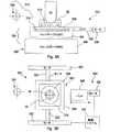
図2には、本発明の一実施形態を示すリソグラフィマシンの断面図が示されている。リソグラフィマシン200は、光学アセンブリ16と、ウェハテーブル204及びウェハステージ206を有するステージアセンブリ202とを備える。ウェハテーブル204は、光学アセンブリ16の下方にウェハ208(もしくは他のタイプのワークピース)を支持するように構成されている。光学アセンブリ16を取り囲む環境システム26は、ウェハ208と光学アセンブリ16の終端の光学素子との間のギャップに液浸流体212を供給し、そこから液浸流体212を除去するために用いられる。ウェハローダ218(例えばロボット)及びアライメントツール220(例えば顕微鏡及びCCDカメラ)を備えるワークピース交換システム216は、ウェハテーブル204上のウェハ208を取り出し、それを第2ウェハに置換するように構成されている。このことは、典型的には、ウェハ208をウェハテーブル204から持ち上げて取り出すためのウェハローダ218を用いて達成される。続いて、第2ウェハ(不図示)は、ウェハチャック218上に置かれ、アライメントツール220を用いてアライメントが行われ、その後ウェハテーブル204上で光学アセンブリ16の下方に位置付けられる。 FIG. 2 shows a cross-sectional view of a lithography machine showing an embodiment of the present invention. The
この実施形態において、ウェハステージ206は、ウェハ交換中に光学アセンブリ16の終端の光学素子に隣接するギャップに液浸流体212を維持するように構成される液浸流体維持システム214を含む。液浸流体維持システム214は、ウェハテーブル204に隣接するパッド222を含む。パッド222とウェハステージ206の間に設けられた支持部材224は、パッド222を支持するために用いられる。ウェハテーブル204は、ウェハ208の表面と面一である平坦な上面を有する。パッド222も、ウェハテーブル204の上面及びウェハ表面に面一である平坦な上面を有する。パッド222は、非常に小さなギャップ(例えば0.1−1.0mm)でウェハテーブル204に隣接して配置されるので、液浸流体212はウェハテーブル204とパッド222の間を漏れることなく移動することができる。ウェハ交換の間、ウェハステージ206は矢印226の向きに移動し、パッド222は、流体をギャップに維持しつつ、または流体ギャップのサイズを維持しつつ、ウェハテーブル204の代わりに光学アセンブリ16の下方に位置付けられる。新しいウェハが位置決めされた後、ウェハステージは元の位置に戻り、パッド222はギャップから取り出されて、第2ウェハが光学アセンブリ16の下方に位置付けられる。様々な実施形態において、パッド222はウェハテーブル204に隙間なく密着して配置される。ウェハテーブル204の垂直方向の位置及び/又は傾きは調整可能であり、ウェハテーブル204が光学アセンブリ16の下方から送り出される前は、ウェハテーブルの表面はパッド表面と面一である。パッド222と光学アセンブリ16の間のギャップを維持することは、ウェハ交換の操作のみに限られない。パッド222は、アライメント操作中もしくは測定操作中に、パッド222と光学アセンブリ16との間の隙間に液浸流体212を維持するための十分な大きさにすることができる。これらの動作において、液浸流体212で占められる領域の一部はウェハテーブル204の上面にあってもよい。 In this embodiment, the
図3A及び3Bには、本発明の別の実施形態に係る別の液浸リソグラフィマシンの断面図及び平面図が示されている。リソグラフィマシン300は、光学アセンブリ16と、ウェハテーブル304及びウェハステージ306を含むステージアセンブリ302とを含む。ウェハテーブル304は、ウェハ308(もしくは別のタイプのワークピース)を光学アセンブリ16の下方に支持するように構成されている。光学アセンブリ16を取り囲む環境システム26を用いて、ウェハ308と光学アセンブリ16の最下部の光学素子との間のギャップに液浸流体312を供給し、そこから液浸流体312を除去する。ウェハーローダー318とアライメントツール320を含むワークピース交換システム316は、ウェハテーブル304上のウェハ308を取り出し、それを第2ウェハに置き換えるように構成されている。このことはウェハテーブル304からウェハ308を取り出すためにウェハローダー318を使用することによって達成される。続いて、第2ウェハ(不図示)がウェハチャック318上に置かれ、アライメントツール320を用いてアライメントされ、その後、光学アセンブリ16の下方に位置付けられる。図3Bに最も分かり易く示されるように、モーターの組322を用いて、ウェハテーブル304及びウェハステージ306を含むウェハアセンブリ302を、操作中に2つの自由度(X及びY)で駆動する。上で述べたように、モーター322は、リニアモーター、ロータリーモーター、ボイスコイルモーターのような任意のタイプのモーターにすることができる。 3A and 3B show a cross-sectional view and a plan view of another immersion lithography machine according to another embodiment of the present invention. The
液浸リソグラフィマシン300はまた、ウェハテーブル304が光学アセンブリの下方から離れている間、光学アセンブリ16の下方の空間に液浸流体312を維持するように構成される液浸流体維持システム324を含む。液浸流体維持システム324は、パッド326、モーター328及び制御システム330を含む。パッド326は、光学アセンブリ16とウェハテーブル204に隣接して位置決めすることができる。ウェハテーブル304は、ウェハ308の上面と面一である平坦な上面を有する。パッド326は、ウェハテーブル304の上面及びウェハ表面と面一である平坦な上面を有する。パッド326は、制御システム330により制御されるモーター328を用いて、X及びY方向に移動可能である。モーター328は、モーター322と同様に任意のタイプのモーターも使用することができる。ウェハテーブル304(ウェハステージ306)が光学アセンブリ16の下方から離れているときに、パッド326は光学アセンブリ16の下方に位置付けられる。ウェハ交換の間、ウェハテーブル304は光学アセンブリ16から遠ざかる。同時に、制御システム330は、モーター328に光学アセンブリ16の下にウェハテーブル308に代わってパッド326を移動させるように指令する。このようにして、パッド326は光学アセンブリ16の下方のギャップに液浸流体312を維持する。新しいウェハがアライメントツール320を用いてアライメントされた後、ウェハテーブル304は光学アセンブリ16の下方に再び位置付けられる。同時に、制御システム330は、モーター328に液浸流体312の漏出を防ぎつつ、ギャップからパッド326を撤退するように指令する。ウェハ交換操作中に、制御システム330はウェハテーブル304とパッド326の間を小さなギャップに維持しつつ、ウェハテーブル304とパッド326を駆動し、その間に光学アセンブリ16の下方の液浸流体312がウェハテーブル304とパッド326の間を移動する。したがって、液浸流体維持システム324はウェハ交換の間、ギャップに液浸流体312を維持する。この実施形態において、ウェハテーブル304(ウェハステージ306)及びパッド326は個別に動作可能である。それゆえ、液浸流体312がパッド326と光学アセンブリ16との間の空間に維持されている間、ウェハテーブル326は自由に移動可能である。本発明の様々な実施形態において、制御システム330は分離した制御システムにしてもよく、またはウェハステージ302及びウェハテーブル304を位置決めするためのモーター322を制御するために用いる制御システムに組み込むこともできる。ウェハテーブル304とパッド326の少なくとも一方の垂直方向の位置及び/又は傾きを調整して、ウェハテーブルが光学アセンブリの下方から送り出される前に、ウェハテーブルの表面をパッドの表面と面一にしてもよい。ウェハテーブル304を光学アセンブリ16から遠ざける操作は、ウェハ交換の操作に限定される必要はない。例えば、アライメント操作、測定操作もしくは他の操作を、パッド326と光学アセンブリ16との間の空間に液浸流体312を維持している間に実行しうる。 The
図4A及び4Bを参照すると、液浸リソグラフィマシンの2つの断面図が示されている。リソグラフィマシン400は、光学アセンブリ16と、ウェハテーブル404及びウェハステージ406を含むステージアセンブリ402とを備える。ウェハテーブル404は光学アセンブリ16の下方にウェハ408(または他のタイプのワークピース)を支持するように構成されている。光学アセンブリ16を取り囲む環境システム26は、ウェハ408と光学アセンブリ16の最下部の光学素子の間のギャップに液浸流体412を供給し、そこから液浸流体412を除去するのに用いられる。ウェハローダー418とアライメントツール420を含むワークピース交換システム416は、ウェハテーブル404上のウェハ408を取り出して、第2ウェハに置き換えるように構成されている。このことは、ウェハローダー418を用いてウェハテーブル404からウェハ408を取り出すことによって達成される。続いて、第2ウェハ(不図示)がウェハチャック418上に置かれ、アライメントツール420を用いてアライメントされ、その後、図4Aに示されるように光学アセンブリ16の下方に位置付けられる。 4A and 4B, two cross-sectional views of an immersion lithography machine are shown. The
液浸リソグラフィマシン400はまた、ウェハテーブル404が光学アセンブリ16の下方から離れている間、光学アセンブリ16の下方の空間に液浸流体412を維持するように構成される液浸流体維持システム424を含む。液浸流体維持システム424は、パッド426と、光学アセンブリ16に設置される第1クランプ428と、ウェハテーブル404に設置される第2クランプ430とを含む。液浸流体412が光学アセンブリ16とウェハテーブル404(またはウェハ408)の間にあるとき、パッド426はウェハテーブル404上の適切な位置に第2クランプ430によって保持される。例えばウェハ交換操作の間のように、ウェハテーブル404が光学アセンブリ16から離れているとき、パッド426はウェハテーブル404から脱離して第1クランプ428によって保持され、光学アセンブリ16とパッド426との間に液浸流体412を維持する。ウェハテーブル404は、ウェハ408の表面と面一である平坦な上面を有する。ウェハテーブル404上に支持されるパッド426もまた、ウェハテーブル404の上面とウェハ表面に面一である平坦な上面を有する。したがって、液浸パッド426とウェハ408は、液浸流体をリークすることなく光学アセンブリの下方で移動することが可能である。様々な実施形態において、クランプ428及び430は、真空クランプ、磁気クランプ、静電クランプもしくはメカニカルクランプにすることができる。 The
図4Aに最良に示されているように、ウェハ408の露光中、パッド426はウェハテーブル404上に位置付けられる。第2クランプ430を用いてウェハの露光中にテーブル404上の適切な位置にパッド426を保持する。図4Bに示されるようなウェハの交換中に、ウェハテーブル404は矢印432の向きに移動して、パッド432をウェハ408の代わりに光学アセンブリ16の下方に位置付ける。この場合には、パッド426をウェハテーブル404に保持している第2クランプ430は開放しつつ、第1クランプ428がパッド426を光学アセンブリ16にクランプする。その結果、ウェハ408が交換される間、液浸流体412は光学アセンブリの下方に維持される。新しいウェハがアライメントされた後、ウェハテーブル404は矢印432と逆の向きに移動して、新しいウェハが光学アセンブリの下方に位置付けられる。この動作に先立って、第1クランプ428は開放されつつ、第2クランプ430が再びパッド426をウェハテーブル404に固定する。本実施形態においては、第1クランプ428によってパッド426がクランプされている間、ウェハテーブル404は自由に移動可能である。 As best shown in FIG. 4A, the
様々な実施形態において、パッド426が第1クランプ428によってクランプされる動作は、ウェハ交換動作のみに限られない。アライメント動作、測定動作、もしくは他の動作は、液浸流体312が光学アセンブリ16と第1クランプ428により固定されているパッド426との間の空間に維持されている間に実行することができる。また、クランプ428はフレーム12又は他の支持部材に設けることができ、クランプ430はウェハステージ406上に設けることができる。パッド426はステージアセンブリ402以外の可動部材上に保持することができる。 In various embodiments, the operation in which the
図5A及び5Bは、本発明の他の実施形態に従う、2つの異なるツインステージ液浸リソグラフィシステムの平面図である。ツインステージリソグラフィシステムの基本的な構造及び操作については、米国特許第6,262,796号及び米国特許第6,341,007号を参照のこと。許容される範囲において、米国特許第6,262,796号及び米国特許第6,341,007号の開示をここに援用して本文の記載の一部とする。両方の実施形態において、一対のウェハステージW1及びW2が示されている。モーター502を用いて、2つのステージWS1及びWS2を水平方向に移動又は位置決めする。その一方で、モーター504を用いて、ステージWS1及びWS2を垂直方向に移動又は位置決めする。モーター502及び504を用いて一方のステージを光学アセンブリ16の下方に交互に位置付け、別のステージでウェハ交換及び位置決めを行う。光学アセンブリ16の下方のウェハの露光が完了したとき、2つのステージは入れ替えられて、上記のプロセスが繰り返される。図2〜4に関連してこれまでに述べられ且つ例示されたような、光学アセンブリ16の下方のギャップに液浸流体を維持するための本発明の様々な実施形態は、いずれかの構成と共に、いずれかのツインステージの構造に使用することができる。例えば、図2の実施形態に関連して、図5A又は5Bのいずれかの各ウェハステージSW1及びSW2は、パッド222及び支持部材224を含むように変更することができる。図3の実施形態に関連して、単一のパッド326、モーター328及び制御システム330は、光学アセンブリ16に隣接して使用することができる。パッド326はステージSW1及びSW2とは別個に動作可能である。ステージSW1とSW2が入れ替えられている間、光学アセンブリ16の下方に液浸流体312を維持するために、パッド326は光学アセンブリ16の下方に移動する。最後に図4の実施形態に関して、取り外し可能な単一のパッドを用いることができる。ステージSW1及びSW2が入れ替えられる間、図4Bに示されるように、パッド426はギャップに液浸流体を維持するために用いられる。その一方、露光中には、パッドは、露光されているウェハステージ上のウェハテーブルの上にクランプされる。このようにすれば、単一のパッドのみが2つのステージWS1及びWS2に対して必要とされる。その代わりに、以下で説明するように、第2ステージをパッドとして使用することもできる。 5A and 5B are plan views of two different twin stage immersion lithography systems according to other embodiments of the present invention. See US Pat. No. 6,262,796 and US Pat. No. 6,341,007 for the basic structure and operation of a twin stage lithography system. To the extent permitted, the disclosures of US Pat. No. 6,262,796 and US Pat. No. 6,341,007 are incorporated herein by reference. In both embodiments, a pair of wafer stages W1 and W2 are shown. Using the
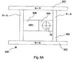
図6Aには、本発明を実施する一つの実施形態を示すツインステージリソグラフィマシンの平面図が示されている。本実施形態において、液浸リソグラフィシステム600は第1ステージ604と第2ステージ606を備える。2つのステージはモーター602によってX及びY方向に移動される。本実施形態においては、ステージ604及び606自体は、ギャップに液浸流体を維持するように用いられる。例えば、図に示されているように、第1ステージ604は光学アセンブリ16の下方に位置付けられる。ワークピースが交換されるときには、モーター602を用いて、第2ステージ606を第2ワークピースと共に、第1ステージ604に隣接して位置決めされる。近接して配置される2つのステージにより、それらは連続的な表面を実質的に形成する。次いで、モーター602を用いて2つのステージを一体的に動かすことにより、第2ステージ604が光学アセンブリ16の下方に位置付けられ、第1ステージはもはや光学アセンブリ16の下方からいなくなる。それゆえ、第1ワークピースが光学アセンブリ16から離れるとき、ギャップの液浸流体は、第1ステージとほぼ連続な面を形成する第2ステージによって維持される。別の様々な実施形態において、第2ステージ606は、第2ワークピースが第1ステージの上に置かれている間、ギャップに液浸流体を維持するために用いられるパッドを備える"パッド"ステージとすることも可能である。同様に、図5A又は5Bのいずれかに示されるモーターの構成を用いることが可能である。 FIG. 6A shows a plan view of a twin stage lithography machine showing one embodiment for carrying out the present invention. In the present embodiment, the
図6B−6Eを参照すると、本発明の実施形態に従うワークピースの交換を表す一連の図が示されている。図6Bは、露光が完了した後のステージ604上のウェハを示す。図6Cは、光学アセンブリ16の下方の第1ステージ604と接している(もしくはすぐ隣にある)第2ステージ606を示している。図6Cは、起こっている配置替え、即ち、第2ステージ606が光学アセンブリ16の下方に位置付けられることを示している。最後に、図6Eにおいて、第1ステージ604は光学アセンブリ16から遠ざかる。図6C及び6Dに最良に図示されるように、2つのステージ604及び606は、配置替えの間、光学アセンブリ16の下方に連続な表面をもたらし、それゆえギャップに液浸流体が維持される。示された実施形態において、第2ステージ606はパッドステージである。しかし、このステージは上述したようにワークピースステージであることも可能である。 With reference to FIGS. 6B-6E, a series of diagrams depicting workpiece replacement in accordance with an embodiment of the present invention is shown. FIG. 6B shows the wafer on
上記の様々な実施形態において、パッドはセラミックス、金属、プラスチックのような複数の異なる材料で作られていてもよい。他の実施形態によれば、これらの材料は、テフロン(登録商標)でコーティングされていてもよい。また、パッドは液浸流体によって占められる領域を覆うのに十分な大きさにするべきである。上記の様々な実施形態において、光学アセンブリ16の終端の光学素子の表面は、流体マーク(いわゆる"ウォーターマーク(awatermark)")の形成を妨げつつ、常に液浸流体の環境下にある。 In the various embodiments described above, the pad may be made of a plurality of different materials such as ceramics, metal, plastic. According to other embodiments, these materials may be coated with Teflon. Also, the pad should be large enough to cover the area occupied by the immersion fluid. In the various embodiments described above, the surface of the optical element at the end of the
半導体ウェハは、上記のシステムを用いて、一般に図7Aに示したプロセスによって製造されることができる。工程701において、ワークピースの機能及び性能特性が設計される。次に、工程702において、パターンを有するマスク(レチクル)が先の設計工程に従って設計され、並行する工程703において、ウェハはシリコン材料で製造される。工程702で設計されたマスクパターンは、工程704において、本発明に従ってこれまでに記載したフォトリソグラフィシステムによって、工程703で製造されたウェハ上に露光される。工程705において、半導体ワークピースは組み立てられ(ダイシング工程、ボンディング工程及びパッケージング工程を含む)、最終的に、ワークピースは工程606において検査される。 A semiconductor wafer can be manufactured using the system described above, generally by the process shown in FIG. 7A. In
図7Bは、半導体ワークピース製造の場合における、上記工程704の詳細なフローチャートの例を示している。図7Bにおいて、工程711(酸化工程)では、ウェハ表面が酸化される。工程712(CVD工程)では、絶縁薄膜がウェハ表面に形成される。工程713(電極形成工程)では、蒸着によってウェハ表面上に電極が形成される。工程714(イオン注入工程)では、イオンがウェハ内に注入される。上記の工程711−714は、ウェハ加工処理中のウェハに対する前処理工程を形成し、加工処理の要請に従って各々の工程が選択される。 FIG. 7B shows an example of a detailed flowchart of
ウェハ加工処理の各々の段階において、前記前処理工程が完了したとき、以下の後処理工程が実行される。後処理工程の間、先ず、工程715(フォトレジスト形成工程)において、フォトレジストがウェハに塗布される。次に、工程716(露光工程)において、上記の露光ワークピースを用いて、マスク(レチクル)の回路パターンをウェハに転写する。その後、工程717(現像工程)において、露光されたウェハが現像され、工程718(エッチング工程)において、残存したフォトレジスト以外の部分(露光された材料表面)がエッチングによって取り除かれる。工程719(フォトレジスト除去工程)において、エッチング後に残存する不必要なフォトレジストが除去される。 At each stage of the wafer processing, when the pre-processing process is completed, the following post-processing process is executed. During the post-processing step, first, in step 715 (photoresist formation step), a photoresist is applied to the wafer. Next, in step 716 (exposure step), the circuit pattern of the mask (reticle) is transferred to the wafer using the exposure workpiece. Thereafter, in step 717 (developing step), the exposed wafer is developed, and in step 718 (etching step), portions other than the remaining photoresist (exposed material surface) are removed by etching. In step 719 (photoresist removal step), unnecessary photoresist remaining after etching is removed.
多重の回路パターンが、これらの前処理工程及び後処理工程を繰り返すことによって形成される。 Multiple circuit patterns are formed by repeating these pre-processing steps and post-processing steps.
本願に示され、開示されている特定のリソグラフィマシンは、十分に目標を達成することができ、本願で以前に述べた利点を十分に提供することができるが、それは単に発明の現時点の好ましい実施形態の例示であり、添付の請求の範囲に記載されたこと以外に、本願に示されている構造や設計の詳細に限定するものではないと解されるべきである。 The particular lithographic machine shown and disclosed in this application can adequately achieve the goals and provide the advantages previously described herein, but it is merely a presently preferred implementation of the invention. It is to be understood that the forms are exemplary and not intended to be limited to the details of construction or design shown herein other than as described in the appended claims.
10…リソグラフィックマシン、16…光学アセンブリ、202…ステージアセンブリ、204…ワークピーステーブル DESCRIPTION OF
Claims (30)
Translated fromJapanese前記基板を保持する基板テーブルと、
前記基板テーブルに保持される基板上に前記露光ビームを投射する投影系と、
前記基板が前記基板テーブルに保持されつつ、前記露光ビームが通る、前記投影系と前記基板との間の空間に供給される液浸液体との接触が解除されるとき、前記投影系の前記液浸液体との接触が維持されるように前記投影系と対向して配置されるパッド部材と、を備え、
前記基板テーブルと前記パッド部材とは相対移動可能である。An immersion exposure apparatus that exposes a substrate with an exposure beam,
A substrate table for holding the substrate;
A projection system for projecting the exposure beam onto a substrate held by the substrate table;
The liquid of the projection system is released when contact with the immersion liquid supplied to the space between the projection system and the substrate through which the exposure beam passes while the substrate is held on the substrate table A pad member disposed opposite the projection system so as to maintain contact with the immersion liquid, and
The substrate table and the pad member are movable relative to each other.
前記基板テーブルによって前記基板が前記投影系の下から離れて移動される間、前記パッド部材は、前記投影系の前記液浸液体との接触を維持する。The immersion exposure apparatus according to claim 1, wherein
The pad member maintains contact with the immersion liquid of the projection system while the substrate is moved away from under the projection system by the substrate table.
前記投影系と前記パッド部材との間に前記液浸液体が維持されるように、前記パッド部材は、前記基板の代わりに前記投影系と対向して配置される。The immersion exposure apparatus according to claim 1 or 2,
The pad member is disposed opposite the projection system instead of the substrate so that the immersion liquid is maintained between the projection system and the pad member.
前記パッド部材はその表面が前記投影系と対向する前記基板の表面と実質的に同一面となるように配置される。In the immersion exposure apparatus according to any one of claims 1 to 3,
The pad member is disposed so that the surface thereof is substantially flush with the surface of the substrate facing the projection system.
前記基板テーブルはステージに設けられ、
前記パッド部材は、前記ステージによって前記投影系と対向して配置される。In the immersion exposure apparatus according to any one of claims 1 to 4,
The substrate table is provided on a stage;
The pad member is arranged to face the projection system by the stage.
前記パッド部材が前記投影系と対向して配置される間、前記基板は、前記投影系の下から離れて配置される。In the immersion exposure apparatus according to claim 5,
While the pad member is disposed opposite the projection system, the substrate is disposed away from the bottom of the projection system.
前記パッド部材は、前記ステージに設けられるとともに、前記ステージによって前記投影系と対向して配置される。The immersion exposure apparatus according to claim 5 or 6,
The pad member is provided on the stage and is disposed to face the projection system by the stage.
前記パッド部材は、前記パッド部材の表面が前記ステージに保持される前記基板の表面と実質的に同一面となるように前記ステージに設けられる。In the immersion exposure apparatus according to any one of claims 5 to 7,
The pad member is provided on the stage so that the surface of the pad member is substantially flush with the surface of the substrate held on the stage.
前記パッド部材が前記投影系と対向して配置されるように、前記パッド部材をリリース可能に保持する保持部材を、さらに備える。In the immersion exposure apparatus according to any one of claims 1 to 5,
A holding member that holds the pad member in a releasable manner so as to face the projection system is further provided.
前記保持部材によって前記パッド部材が保持される間、前記基板は、前記投影系の下から離れて配置される。The immersion exposure apparatus according to claim 9, wherein
While the pad member is held by the holding member, the substrate is disposed away from the bottom of the projection system.
前記保持部材は、前記パッド部材をバキュームで保持する。The immersion exposure apparatus according to claim 9 or 10,
The holding member holds the pad member in a vacuum.
前記基板テーブルは、前記パッド部材をリリース可能に保持する保持部を有する。In the immersion exposure apparatus according to any one of claims 9 to 11,
The substrate table includes a holding portion that holds the pad member in a releasable manner.
前記基板が前記投影系と対向して配置される間、前記パッド部材は、前記保持部で保持される。The immersion exposure apparatus according to claim 12, wherein
While the substrate is disposed facing the projection system, the pad member is held by the holding portion.
前記パッド部材が前記投影系との間に前記液浸液体を維持するように、前記投影系に対して前記基板テーブルを相対移動するコントローラを、さらに備える。In the immersion exposure apparatus according to any one of claims 1 to 13,
The apparatus further includes a controller for moving the substrate table relative to the projection system such that the pad member maintains the immersion liquid between the pad member and the projection system.
請求項1〜14のいずれか一項に記載の液浸露光装置を用いて、投影系と、前記投影系と基板との間の空間に供給される液浸液体とを介して露光ビームで前記基板を露光することと、
前記基板と前記液浸液体との接触が解除されるとき、前記投影系の前記液浸液体との接触が維持されるように前記投影系と対向してパッド部材を配置することと、を含む。A device manufacturing method comprising:
The immersion exposure apparatus according to any one of claims 1 to 14, wherein the exposure beam is used as an exposure beam via a projection system and an immersion liquid supplied to a space between the projection system and the substrate. Exposing the substrate;
Disposing a pad member facing the projection system such that contact with the immersion liquid of the projection system is maintained when contact between the substrate and the immersion liquid is released. .
投影系と基板との間の空間に液浸液体を供給することと、
前記投影系と前記液浸液体とを介して前記基板上に露光ビームを投射することと、
前記基板が基板テーブルに保持されつつ前記液浸液体との接触が解除されるとき、前記投影系の前記液浸液体との接触が維持されるように前記投影系と対向して、前記基板テーブルと相対移動可能なパッド部材を配置することと、を含む。A device manufacturing method comprising:
Supplying immersion liquid to a space between the projection system and the substrate;
Projecting an exposure beam onto the substrate via the projection system and the immersion liquid;
When the substrate is held on the substrate table and the contact with the immersion liquid is released, the substrate table faces the projection system so that the contact with the immersion liquid is maintained. And disposing a relatively movable pad member.
前記基板が前記投影系の下から離れて移動される間、前記パッド部材は、前記投影系の前記液浸液体との接触を維持する。The method of claim 16, wherein
While the substrate is moved away from below the projection system, the pad member maintains contact with the immersion liquid of the projection system.
前記投影系と前記パッド部材との間に前記液浸液体が維持されるように、前記パッド部材は、前記投影系の前記液浸液体との接触を維持するために前記投影系と対向して配置される。The method according to claim 16 or 17, wherein
The pad member is opposed to the projection system to maintain contact with the immersion liquid of the projection system so that the immersion liquid is maintained between the projection system and the pad member. Be placed.
前記パッド部材はその表面が前記投影系と対向する前記基板の表面と実質的に同一面となるように配置される。The method according to any one of claims 16 to 18, wherein
The pad member is disposed so that the surface thereof is substantially flush with the surface of the substrate facing the projection system.
前記パッド部材は、前記基板テーブルが設けられるステージによって前記投影系と対向して配置される。The method according to any one of claims 16 to 19, wherein
The pad member is disposed to face the projection system by a stage on which the substrate table is provided.
前記パッド部材が前記投影系と対向して配置される間、前記基板は、前記投影系の下から離れて配置される。The method of claim 20, wherein
While the pad member is disposed opposite the projection system, the substrate is disposed away from the bottom of the projection system.
前記パッド部材は、前記ステージに設けられるとともに、前記ステージによって前記投影系と対向して配置される。The method according to claim 20 or 21, wherein
The pad member is provided on the stage and is disposed to face the projection system by the stage.
前記パッド部材は、前記パッド部材の表面が前記ステージに保持される前記基板の表面と実質的に同一面となるように前記ステージに設けられる。23. A method according to any one of claims 20-22,
The pad member is provided on the stage so that the surface of the pad member is substantially flush with the surface of the substrate held on the stage.
前記パッド部材は、前記投影系と対向して配置されるようにリリース可能に保持される。21. A method according to any one of claims 16-20,
The pad member is releasably held so as to be disposed to face the projection system.
前記投影系と対向して前記パッド部材が保持される間、前記基板は、前記投影系の下から離れて配置される。25. The method of claim 24, wherein
While the pad member is held facing the projection system, the substrate is disposed away from the bottom of the projection system.
前記パッド部材はバキュームで保持される。The method according to claim 24 or 25, wherein:
The pad member is held in a vacuum.
前記パッド部材は、前記基板テーブルによってリリース可能に保持される。A method according to any one of claims 24-26,
The pad member is releasably held by the substrate table.
前記基板が前記投影系と対向して配置される間、前記パッド部材は、前記基板テーブルに保持される。28. The method of claim 27, wherein
The pad member is held on the substrate table while the substrate is disposed opposite the projection system.
前記パッド部材が前記投影系との間に前記液浸液体を維持するように、前記基板テーブルは、前記投影系に対して相対移動される。In the immersion exposure apparatus according to any one of claims 16 to 28,
The substrate table is moved relative to the projection system such that the pad member maintains the immersion liquid between it and the projection system.
前記液浸液体は、前記投影系と前記基板との間の空間に供給される。The immersion exposure apparatus according to any one of claims 16 to 29,
The immersion liquid is supplied to a space between the projection system and the substrate.
Applications Claiming Priority (2)
| Application Number | Priority Date | Filing Date | Title |
|---|---|---|---|
| US46249903P | 2003-04-11 | 2003-04-11 | |
| US60/462,499 | 2003-04-11 |
Related Parent Applications (1)
| Application Number | Title | Priority Date | Filing Date |
|---|---|---|---|
| JP2011266301ADivisionJP5660016B2 (en) | 2003-04-11 | 2011-12-05 | Immersion exposure apparatus, immersion exposure method, and device manufacturing method |
Related Child Applications (1)
| Application Number | Title | Priority Date | Filing Date |
|---|---|---|---|
| JP2015010863ADivisionJP5900669B2 (en) | 2003-04-11 | 2015-01-23 | Immersion lithography apparatus and device manufacturing method |
Publications (2)
| Publication Number | Publication Date |
|---|---|
| JP2014222762Atrue JP2014222762A (en) | 2014-11-27 |
| JP5862716B2 JP5862716B2 (en) | 2016-02-16 |
Family
ID=33159850
Family Applications (12)
| Application Number | Title | Priority Date | Filing Date |
|---|---|---|---|
| JP2006506525AExpired - Fee RelatedJP4315198B2 (en) | 2003-04-11 | 2004-03-17 | Lithographic apparatus for maintaining immersion liquid under an optical assembly, immersion liquid maintenance method and device manufacturing method using them |
| JP2008111219AExpired - Fee RelatedJP4775402B2 (en) | 2003-04-11 | 2008-04-22 | Immersion exposure apparatus, immersion exposure method, device manufacturing method, and immersion exposure apparatus manufacturing method |
| JP2010012365AExpired - Fee RelatedJP4952804B2 (en) | 2003-04-11 | 2010-01-22 | Immersion exposure apparatus and immersion exposure method |
| JP2011112549AExpired - Fee RelatedJP5440551B2 (en) | 2003-04-11 | 2011-05-19 | Immersion exposure apparatus, immersion exposure method, and device manufacturing method |
| JP2011266300AExpired - Fee RelatedJP5556798B2 (en) | 2003-04-11 | 2011-12-05 | Immersion exposure apparatus, immersion exposure method, and device manufacturing method |
| JP2011266301AExpired - Fee RelatedJP5660016B2 (en) | 2003-04-11 | 2011-12-05 | Immersion exposure apparatus, immersion exposure method, and device manufacturing method |
| JP2012078264AExpired - Fee RelatedJP5556840B2 (en) | 2003-04-11 | 2012-03-29 | Immersion exposure apparatus, immersion exposure method, and device manufacturing method |
| JP2013127364AExpired - LifetimeJP5510596B2 (en) | 2003-04-11 | 2013-06-18 | Immersion lithography apparatus and device manufacturing method |
| JP2014136910AExpired - Fee RelatedJP5862716B2 (en) | 2003-04-11 | 2014-07-02 | Immersion lithography apparatus and device manufacturing method |
| JP2015010863AExpired - Fee RelatedJP5900669B2 (en) | 2003-04-11 | 2015-01-23 | Immersion lithography apparatus and device manufacturing method |
| JP2015127873AExpired - Fee RelatedJP6028838B2 (en) | 2003-04-11 | 2015-06-25 | Immersion lithography apparatus and device manufacturing method |
| JP2016026294AExpired - Fee RelatedJP6090486B2 (en) | 2003-04-11 | 2016-02-15 | Immersion lithography apparatus and device manufacturing method |
Family Applications Before (8)
| Application Number | Title | Priority Date | Filing Date |
|---|---|---|---|
| JP2006506525AExpired - Fee RelatedJP4315198B2 (en) | 2003-04-11 | 2004-03-17 | Lithographic apparatus for maintaining immersion liquid under an optical assembly, immersion liquid maintenance method and device manufacturing method using them |
| JP2008111219AExpired - Fee RelatedJP4775402B2 (en) | 2003-04-11 | 2008-04-22 | Immersion exposure apparatus, immersion exposure method, device manufacturing method, and immersion exposure apparatus manufacturing method |
| JP2010012365AExpired - Fee RelatedJP4952804B2 (en) | 2003-04-11 | 2010-01-22 | Immersion exposure apparatus and immersion exposure method |
| JP2011112549AExpired - Fee RelatedJP5440551B2 (en) | 2003-04-11 | 2011-05-19 | Immersion exposure apparatus, immersion exposure method, and device manufacturing method |
| JP2011266300AExpired - Fee RelatedJP5556798B2 (en) | 2003-04-11 | 2011-12-05 | Immersion exposure apparatus, immersion exposure method, and device manufacturing method |
| JP2011266301AExpired - Fee RelatedJP5660016B2 (en) | 2003-04-11 | 2011-12-05 | Immersion exposure apparatus, immersion exposure method, and device manufacturing method |
| JP2012078264AExpired - Fee RelatedJP5556840B2 (en) | 2003-04-11 | 2012-03-29 | Immersion exposure apparatus, immersion exposure method, and device manufacturing method |
| JP2013127364AExpired - LifetimeJP5510596B2 (en) | 2003-04-11 | 2013-06-18 | Immersion lithography apparatus and device manufacturing method |
Family Applications After (3)
| Application Number | Title | Priority Date | Filing Date |
|---|---|---|---|
| JP2015010863AExpired - Fee RelatedJP5900669B2 (en) | 2003-04-11 | 2015-01-23 | Immersion lithography apparatus and device manufacturing method |
| JP2015127873AExpired - Fee RelatedJP6028838B2 (en) | 2003-04-11 | 2015-06-25 | Immersion lithography apparatus and device manufacturing method |
| JP2016026294AExpired - Fee RelatedJP6090486B2 (en) | 2003-04-11 | 2016-02-15 | Immersion lithography apparatus and device manufacturing method |
Country Status (9)
| Country | Link |
|---|---|
| US (18) | US7372538B2 (en) |
| EP (8) | EP3141953A3 (en) |
| JP (12) | JP4315198B2 (en) |
| KR (15) | KR101225884B1 (en) |
| CN (3) | CN101980086B (en) |
| IL (5) | IL170735A (en) |
| SG (12) | SG139734A1 (en) |
| TW (16) | TWI545387B (en) |
| WO (1) | WO2004090577A2 (en) |
Families Citing this family (222)
| Publication number | Priority date | Publication date | Assignee | Title |
|---|---|---|---|---|
| EP1420299B1 (en) | 2002-11-12 | 2011-01-05 | ASML Netherlands B.V. | Immersion lithographic apparatus and device manufacturing method |
| US10503084B2 (en) | 2002-11-12 | 2019-12-10 | Asml Netherlands B.V. | Lithographic apparatus and device manufacturing method |
| US7372541B2 (en) | 2002-11-12 | 2008-05-13 | Asml Netherlands B.V. | Lithographic apparatus and device manufacturing method |
| DE60335595D1 (en) | 2002-11-12 | 2011-02-17 | Asml Netherlands Bv | Immersion lithographic apparatus and method of making a device |
| CN100568101C (en) | 2002-11-12 | 2009-12-09 | Asml荷兰有限公司 | Photolithography apparatus and device manufacturing method |
| US7110081B2 (en) | 2002-11-12 | 2006-09-19 | Asml Netherlands B.V. | Lithographic apparatus and device manufacturing method |
| KR100585476B1 (en) | 2002-11-12 | 2006-06-07 | 에이에스엠엘 네델란즈 비.브이. | Lithographic Apparatus and Device Manufacturing Method |
| US9482966B2 (en) | 2002-11-12 | 2016-11-01 | Asml Netherlands B.V. | Lithographic apparatus and device manufacturing method |
| SG121822A1 (en)* | 2002-11-12 | 2006-05-26 | Asml Netherlands Bv | Lithographic apparatus and device manufacturing method |
| KR101101737B1 (en) | 2002-12-10 | 2012-01-05 | 가부시키가이샤 니콘 | Exposure apparatus, exposure method and method for manufacturing device |
| US7948604B2 (en) | 2002-12-10 | 2011-05-24 | Nikon Corporation | Exposure apparatus and method for producing device |
| EP1571694A4 (en) | 2002-12-10 | 2008-10-15 | Nikon Corp | Exposure apparatus and method for manufacturing device |
| US7242455B2 (en) | 2002-12-10 | 2007-07-10 | Nikon Corporation | Exposure apparatus and method for producing device |
| KR20120127755A (en) | 2002-12-10 | 2012-11-23 | 가부시키가이샤 니콘 | Exposure apparatus and method for manufacturing device |
| WO2004053955A1 (en) | 2002-12-10 | 2004-06-24 | Nikon Corporation | Exposure system and device producing method |
| JP4352874B2 (en) | 2002-12-10 | 2009-10-28 | 株式会社ニコン | Exposure apparatus and device manufacturing method |
| DE10261775A1 (en) | 2002-12-20 | 2004-07-01 | Carl Zeiss Smt Ag | Device for the optical measurement of an imaging system |
| EP2466623B1 (en) | 2003-02-26 | 2015-04-22 | Nikon Corporation | Exposure apparatus, exposure method, and method for producing device |
| KR20050110033A (en) | 2003-03-25 | 2005-11-22 | 가부시키가이샤 니콘 | Exposure system and device production method |
| EP1612850B1 (en) | 2003-04-07 | 2009-03-25 | Nikon Corporation | Exposure apparatus and method for manufacturing a device |
| WO2004093159A2 (en) | 2003-04-09 | 2004-10-28 | Nikon Corporation | Immersion lithography fluid control system |
| EP2950147B1 (en) | 2003-04-10 | 2017-04-26 | Nikon Corporation | Environmental system including vaccum scavenge for an immersion lithography apparatus |
| EP3062152B1 (en) | 2003-04-10 | 2017-12-20 | Nikon Corporation | Environmental system including vaccum scavenge for an immersion lithography apparatus |
| EP3352010A1 (en) | 2003-04-10 | 2018-07-25 | Nikon Corporation | Run-off path to collect liquid for an immersion lithography apparatus |
| KR101225884B1 (en)* | 2003-04-11 | 2013-01-28 | 가부시키가이샤 니콘 | Apparatus and method for maintaining immersion fluid in the gap under the projection lens during wafer exchange in an immersion lithography machine |
| CN101825847B (en) | 2003-04-11 | 2013-10-16 | 株式会社尼康 | Cleanup method for optics in immersion lithography |
| JP4582089B2 (en) | 2003-04-11 | 2010-11-17 | 株式会社ニコン | Liquid jet recovery system for immersion lithography |
| SG194246A1 (en) | 2003-04-17 | 2013-11-29 | Nikon Corp | Optical arrangement of autofocus elements for use with immersion lithography |
| TWI295414B (en) | 2003-05-13 | 2008-04-01 | Asml Netherlands Bv | Lithographic apparatus and device manufacturing method |
| KR20060009356A (en) | 2003-05-15 | 2006-01-31 | 가부시키가이샤 니콘 | Exposure apparatus and device manufacturing method |
| TW201806001A (en) | 2003-05-23 | 2018-02-16 | 尼康股份有限公司 | Exposure device and device manufacturing method |
| TWI421906B (en) | 2003-05-23 | 2014-01-01 | 尼康股份有限公司 | An exposure method, an exposure apparatus, and an element manufacturing method |
| KR101548832B1 (en) | 2003-05-28 | 2015-09-01 | 가부시키가이샤 니콘 | Exposure method, exposure device, and device manufacturing method |
| US7213963B2 (en) | 2003-06-09 | 2007-05-08 | Asml Netherlands B.V. | Lithographic apparatus and device manufacturing method |
| EP2261741A3 (en) | 2003-06-11 | 2011-05-25 | ASML Netherlands B.V. | Lithographic apparatus and device manufacturing method |
| US7317504B2 (en) | 2004-04-08 | 2008-01-08 | Asml Netherlands B.V. | Lithographic apparatus and device manufacturing method |
| KR101242815B1 (en) | 2003-06-13 | 2013-03-12 | 가부시키가이샤 니콘 | Exposure method, substrate stage, exposure apparatus and method for manufacturing device |
| US6867844B2 (en) | 2003-06-19 | 2005-03-15 | Asml Holding N.V. | Immersion photolithography system and method using microchannel nozzles |
| TW201721717A (en) | 2003-06-19 | 2017-06-16 | 尼康股份有限公司 | Exposure apparatus, exposure method, and device manufacturing method |
| JP3862678B2 (en) | 2003-06-27 | 2006-12-27 | キヤノン株式会社 | Exposure apparatus and device manufacturing method |
| US6809794B1 (en) | 2003-06-27 | 2004-10-26 | Asml Holding N.V. | Immersion photolithography system and method using inverted wafer-projection optics interface |
| EP1491956B1 (en) | 2003-06-27 | 2006-09-06 | ASML Netherlands B.V. | Lithographic apparatus and device manufacturing method |
| KR20060027832A (en) | 2003-07-01 | 2006-03-28 | 가부시키가이샤 니콘 | Method of Using Isotopically Specified Fluids as Optical Elements |
| EP3179309A1 (en) | 2003-07-08 | 2017-06-14 | Nikon Corporation | Wafer table for immersion lithography |
| EP1643543B1 (en) | 2003-07-09 | 2010-11-24 | Nikon Corporation | Exposure apparatus and method for manufacturing device |
| WO2005006415A1 (en) | 2003-07-09 | 2005-01-20 | Nikon Corporation | Exposure apparatus and method for manufacturing device |
| WO2005006418A1 (en) | 2003-07-09 | 2005-01-20 | Nikon Corporation | Exposure apparatus and method for manufacturing device |
| WO2005010960A1 (en) | 2003-07-25 | 2005-02-03 | Nikon Corporation | Inspection method and inspection device for projection optical system, and production method for projection optical system |
| EP1503244A1 (en) | 2003-07-28 | 2005-02-02 | ASML Netherlands B.V. | Lithographic projection apparatus and device manufacturing method |
| KR101641011B1 (en) | 2003-07-28 | 2016-07-19 | 가부시키가이샤 니콘 | Exposure apparatus, device producing method, and exposure apparatus controlling method |
| US7175968B2 (en) | 2003-07-28 | 2007-02-13 | Asml Netherlands B.V. | Lithographic apparatus, device manufacturing method and a substrate |
| US7326522B2 (en) | 2004-02-11 | 2008-02-05 | Asml Netherlands B.V. | Device manufacturing method and a substrate |
| US7779781B2 (en) | 2003-07-31 | 2010-08-24 | Asml Netherlands B.V. | Lithographic apparatus and device manufacturing method |
| TWI263859B (en) | 2003-08-29 | 2006-10-11 | Asml Netherlands Bv | Lithographic apparatus and device manufacturing method |
| KR101380989B1 (en) | 2003-08-29 | 2014-04-04 | 가부시키가이샤 니콘 | Exposure apparatus and device producing method |
| EP3223053A1 (en) | 2003-09-03 | 2017-09-27 | Nikon Corporation | Apparatus and method for providing fluid for immersion lithography |
| JP4444920B2 (en) | 2003-09-19 | 2010-03-31 | 株式会社ニコン | Exposure apparatus and device manufacturing method |
| EP2837969B1 (en) | 2003-09-29 | 2016-04-20 | Nikon Corporation | Exposure apparatus, exposure method, and method for producing device |
| JP2005136364A (en) | 2003-10-08 | 2005-05-26 | Zao Nikon Co Ltd | Substrate transport apparatus, exposure apparatus, and device manufacturing method |
| KR101203028B1 (en) | 2003-10-08 | 2012-11-21 | 가부시키가이샤 자오 니콘 | Substrate carrying apparatus, substrate carrying method, exposure apparatus, exposure method, and method for producing device |
| KR20060126949A (en) | 2003-10-08 | 2006-12-11 | 가부시키가이샤 니콘 | Substrate conveyance apparatus and substrate conveyance method, exposure apparatus, exposure method, and device manufacturing method |
| TWI553701B (en) | 2003-10-09 | 2016-10-11 | 尼康股份有限公司 | Exposure apparatus and exposure method, component manufacturing method |
| US7411653B2 (en) | 2003-10-28 | 2008-08-12 | Asml Netherlands B.V. | Lithographic apparatus |
| US7352433B2 (en) | 2003-10-28 | 2008-04-01 | Asml Netherlands B.V. | Lithographic apparatus and device manufacturing method |
| US7528929B2 (en) | 2003-11-14 | 2009-05-05 | Asml Netherlands B.V. | Lithographic apparatus and device manufacturing method |
| KR101394764B1 (en)* | 2003-12-03 | 2014-05-27 | 가부시키가이샤 니콘 | Exposure apparatus, exposure method, device producing method, and optical component |
| JP4720506B2 (en) | 2003-12-15 | 2011-07-13 | 株式会社ニコン | Stage apparatus, exposure apparatus, and exposure method |
| US7394521B2 (en) | 2003-12-23 | 2008-07-01 | Asml Netherlands B.V. | Lithographic apparatus and device manufacturing method |
| DE602005019689D1 (en) | 2004-01-20 | 2010-04-15 | Zeiss Carl Smt Ag | EXPOSURE DEVICE AND MEASURING DEVICE FOR A PROJECTION SECTOR |
| US7589822B2 (en) | 2004-02-02 | 2009-09-15 | Nikon Corporation | Stage drive method and stage unit, exposure apparatus, and device manufacturing method |
| WO2005076321A1 (en) | 2004-02-03 | 2005-08-18 | Nikon Corporation | Exposure apparatus and method of producing device |
| KR101851511B1 (en) | 2004-03-25 | 2018-04-23 | 가부시키가이샤 니콘 | Exposure apparatus and method for manufacturing device |
| US7034917B2 (en) | 2004-04-01 | 2006-04-25 | Asml Netherlands B.V. | Lithographic apparatus, device manufacturing method and device manufactured thereby |
| US7898642B2 (en) | 2004-04-14 | 2011-03-01 | Asml Netherlands B.V. | Lithographic apparatus and device manufacturing method |
| US7400460B2 (en)* | 2004-04-26 | 2008-07-15 | Carl Zeiss Smt Ag | Method for connection of an optical element to a mount structure |
| US8054448B2 (en) | 2004-05-04 | 2011-11-08 | Nikon Corporation | Apparatus and method for providing fluid for immersion lithography |
| US7616383B2 (en) | 2004-05-18 | 2009-11-10 | Asml Netherlands B.V. | Lithographic apparatus and device manufacturing method |
| CN100594430C (en) | 2004-06-04 | 2010-03-17 | 卡尔蔡司Smt股份公司 | System for measuring image quality of optical imaging system |
| EP3203498A1 (en) | 2004-06-09 | 2017-08-09 | Nikon Corporation | Exposure apparatus and device manufacturing method |
| KR101227290B1 (en) | 2004-06-09 | 2013-01-29 | 가부시키가이샤 니콘 | Substrate holding device, exposure apparatus having same, exposure method, method for producing device, and liquid repellent plate |
| US7463330B2 (en) | 2004-07-07 | 2008-12-09 | Asml Netherlands B.V. | Lithographic apparatus and device manufacturing method |
| JP4894515B2 (en) | 2004-07-12 | 2012-03-14 | 株式会社ニコン | Exposure apparatus, device manufacturing method, and liquid detection method |
| US8169591B2 (en)* | 2004-08-03 | 2012-05-01 | Nikon Corporation | Exposure apparatus, exposure method, and method for producing device |
| TW200615716A (en)* | 2004-08-05 | 2006-05-16 | Nikon Corp | Stage device and exposure device |
| KR20070048164A (en) | 2004-08-18 | 2007-05-08 | 가부시키가이샤 니콘 | Exposure apparatus and device manufacturing method |
| US7701550B2 (en) | 2004-08-19 | 2010-04-20 | Asml Netherlands B.V. | Lithographic apparatus and device manufacturing method |
| KR101364347B1 (en)* | 2004-10-15 | 2014-02-18 | 가부시키가이샤 니콘 | Exposure apparatus and device manufacturing method |
| US7119876B2 (en) | 2004-10-18 | 2006-10-10 | Asml Netherlands B.V. | Lithographic apparatus and device manufacturing method |
| CN101598903A (en)* | 2004-11-01 | 2009-12-09 | 株式会社尼康 | Exposure device and exposure method |
| JP4517354B2 (en)* | 2004-11-08 | 2010-08-04 | 株式会社ニコン | Exposure apparatus and device manufacturing method |
| US7583357B2 (en)* | 2004-11-12 | 2009-09-01 | Asml Netherlands B.V. | Lithographic apparatus and device manufacturing method |
| US7411657B2 (en) | 2004-11-17 | 2008-08-12 | Asml Netherlands B.V. | Lithographic apparatus and device manufacturing method |
| TWI588872B (en)* | 2004-11-18 | 2017-06-21 | 尼康股份有限公司 | Position measurement method, position control method, measurement method, loading method, exposure method and exposure apparatus, and device manufacturing method |
| JP4807629B2 (en)* | 2004-11-25 | 2011-11-02 | 株式会社ニコン | Exposure apparatus and device manufacturing method |
| US7446850B2 (en) | 2004-12-03 | 2008-11-04 | Asml Netherlands B.V. | Lithographic apparatus and device manufacturing method |
| JP4784513B2 (en) | 2004-12-06 | 2011-10-05 | 株式会社ニコン | Maintenance method, maintenance equipment, exposure apparatus, and device manufacturing method |
| US7196770B2 (en) | 2004-12-07 | 2007-03-27 | Asml Netherlands B.V. | Prewetting of substrate before immersion exposure |
| US7397533B2 (en) | 2004-12-07 | 2008-07-08 | Asml Netherlands B.V. | Lithographic apparatus and device manufacturing method |
| US7365827B2 (en) | 2004-12-08 | 2008-04-29 | Asml Netherlands B.V. | Lithographic apparatus and device manufacturing method |
| JP4752473B2 (en) | 2004-12-09 | 2011-08-17 | 株式会社ニコン | Exposure apparatus, exposure method, and device manufacturing method |
| US7352440B2 (en) | 2004-12-10 | 2008-04-01 | Asml Netherlands B.V. | Substrate placement in immersion lithography |
| US7403261B2 (en) | 2004-12-15 | 2008-07-22 | Asml Netherlands B.V. | Lithographic apparatus and device manufacturing method |
| US7528931B2 (en) | 2004-12-20 | 2009-05-05 | Asml Netherlands B.V. | Lithographic apparatus and device manufacturing method |
| US7880860B2 (en) | 2004-12-20 | 2011-02-01 | Asml Netherlands B.V. | Lithographic apparatus and device manufacturing method |
| US7405805B2 (en) | 2004-12-28 | 2008-07-29 | Asml Netherlands B.V. | Lithographic apparatus and device manufacturing method |
| US7491661B2 (en) | 2004-12-28 | 2009-02-17 | Asml Netherlands B.V. | Device manufacturing method, top coat material and substrate |
| US20060147821A1 (en) | 2004-12-30 | 2006-07-06 | Asml Netherlands B.V. | Lithographic apparatus and device manufacturing method |
| DE602006012746D1 (en) | 2005-01-14 | 2010-04-22 | Asml Netherlands Bv | Lithographic apparatus and manufacturing method |
| US8692973B2 (en) | 2005-01-31 | 2014-04-08 | Nikon Corporation | Exposure apparatus and method for producing device |
| KR101513840B1 (en) | 2005-01-31 | 2015-04-20 | 가부시키가이샤 니콘 | Exposure apparatus and method for manufacturing device |
| CN102360170B (en) | 2005-02-10 | 2014-03-12 | Asml荷兰有限公司 | Immersion liquid, exposure apparatus, and exposure process |
| US8018573B2 (en) | 2005-02-22 | 2011-09-13 | Asml Netherlands B.V. | Lithographic apparatus and device manufacturing method |
| US7224431B2 (en) | 2005-02-22 | 2007-05-29 | Asml Netherlands B.V. | Lithographic apparatus and device manufacturing method |
| US7378025B2 (en) | 2005-02-22 | 2008-05-27 | Asml Netherlands B.V. | Fluid filtration method, fluid filtered thereby, lithographic apparatus and device manufacturing method |
| US7428038B2 (en) | 2005-02-28 | 2008-09-23 | Asml Netherlands B.V. | Lithographic apparatus, device manufacturing method and apparatus for de-gassing a liquid |
| US7282701B2 (en) | 2005-02-28 | 2007-10-16 | Asml Netherlands B.V. | Sensor for use in a lithographic apparatus |
| US7324185B2 (en) | 2005-03-04 | 2008-01-29 | Asml Netherlands B.V. | Lithographic apparatus and device manufacturing method |
| US7684010B2 (en) | 2005-03-09 | 2010-03-23 | Asml Netherlands B.V. | Lithographic apparatus, device manufacturing method, seal structure, method of removing an object and a method of sealing |
| US7330238B2 (en) | 2005-03-28 | 2008-02-12 | Asml Netherlands, B.V. | Lithographic apparatus, immersion projection apparatus and device manufacturing method |
| JP4544303B2 (en)* | 2005-03-30 | 2010-09-15 | 株式会社ニコン | Exposure apparatus, exposure method, and device manufacturing method |
| US7411654B2 (en) | 2005-04-05 | 2008-08-12 | Asml Netherlands B.V. | Lithographic apparatus and device manufacturing method |
| US7291850B2 (en) | 2005-04-08 | 2007-11-06 | Asml Netherlands B.V. | Lithographic apparatus and device manufacturing method |
| USRE43576E1 (en) | 2005-04-08 | 2012-08-14 | Asml Netherlands B.V. | Dual stage lithographic apparatus and device manufacturing method |
| US20060232753A1 (en) | 2005-04-19 | 2006-10-19 | Asml Holding N.V. | Liquid immersion lithography system with tilted liquid flow |
| EP2527921A3 (en) | 2005-04-28 | 2017-10-18 | Nikon Corporation | Exposure method and exposure apparatus |
| US7317507B2 (en) | 2005-05-03 | 2008-01-08 | Asml Netherlands B.V. | Lithographic apparatus and device manufacturing method |
| US8248577B2 (en) | 2005-05-03 | 2012-08-21 | Asml Netherlands B.V. | Lithographic apparatus and device manufacturing method |
| US7433016B2 (en) | 2005-05-03 | 2008-10-07 | Asml Netherlands B.V. | Lithographic apparatus and device manufacturing method |
| US7751027B2 (en) | 2005-06-21 | 2010-07-06 | Asml Netherlands B.V. | Lithographic apparatus and device manufacturing method |
| US7652746B2 (en) | 2005-06-21 | 2010-01-26 | Asml Netherlands B.V. | Lithographic apparatus and device manufacturing method |
| US7468779B2 (en) | 2005-06-28 | 2008-12-23 | Asml Netherlands B.V. | Lithographic apparatus and device manufacturing method |
| US7834974B2 (en) | 2005-06-28 | 2010-11-16 | Asml Netherlands B.V. | Lithographic apparatus and device manufacturing method |
| US7474379B2 (en) | 2005-06-28 | 2009-01-06 | Asml Netherlands B.V. | Lithographic apparatus and device manufacturing method |
| US7583358B2 (en) | 2005-07-25 | 2009-09-01 | Micron Technology, Inc. | Systems and methods for retrieving residual liquid during immersion lens photolithography |
| EP1918983A4 (en) | 2005-08-05 | 2010-03-31 | Nikon Corp | Stage apparatus and exposure apparatus |
| US8054445B2 (en) | 2005-08-16 | 2011-11-08 | Asml Netherlands B.V. | Lithographic apparatus and device manufacturing method |
| WO2007029829A1 (en)* | 2005-09-09 | 2007-03-15 | Nikon Corporation | Exposure apparatus, exposure method, and device production method |
| US7417710B2 (en)* | 2005-09-26 | 2008-08-26 | Asml Netherlands B.V. | Lithographic apparatus and device manufacturing method |
| JP3997244B2 (en)* | 2005-10-04 | 2007-10-24 | キヤノン株式会社 | Exposure apparatus and device manufacturing method |
| JP4164508B2 (en)* | 2005-10-04 | 2008-10-15 | キヤノン株式会社 | Exposure apparatus and device manufacturing method |
| JP3997245B2 (en)* | 2005-10-04 | 2007-10-24 | キヤノン株式会社 | Exposure apparatus and device manufacturing method |
| US7411658B2 (en) | 2005-10-06 | 2008-08-12 | Asml Netherlands B.V. | Lithographic apparatus and device manufacturing method |
| JPWO2007055237A1 (en)* | 2005-11-09 | 2009-04-30 | 株式会社ニコン | Exposure apparatus, exposure method, and device manufacturing method |
| US7656501B2 (en) | 2005-11-16 | 2010-02-02 | Asml Netherlands B.V. | Lithographic apparatus |
| US7864292B2 (en) | 2005-11-16 | 2011-01-04 | Asml Netherlands B.V. | Lithographic apparatus and device manufacturing method |
| US7804577B2 (en) | 2005-11-16 | 2010-09-28 | Asml Netherlands B.V. | Lithographic apparatus |
| US7633073B2 (en) | 2005-11-23 | 2009-12-15 | Asml Netherlands B.V. | Lithographic apparatus and device manufacturing method |
| US7773195B2 (en) | 2005-11-29 | 2010-08-10 | Asml Holding N.V. | System and method to increase surface tension and contact angle in immersion lithography |
| US8125610B2 (en) | 2005-12-02 | 2012-02-28 | ASML Metherlands B.V. | Method for preventing or reducing contamination of an immersion type projection apparatus and an immersion type lithographic apparatus |
| US7420194B2 (en) | 2005-12-27 | 2008-09-02 | Asml Netherlands B.V. | Lithographic apparatus and substrate edge seal |
| US7839483B2 (en) | 2005-12-28 | 2010-11-23 | Asml Netherlands B.V. | Lithographic apparatus, device manufacturing method and a control system |
| US7649611B2 (en) | 2005-12-30 | 2010-01-19 | Asml Netherlands B.V. | Lithographic apparatus and device manufacturing method |
| US8472004B2 (en)* | 2006-01-18 | 2013-06-25 | Micron Technology, Inc. | Immersion photolithography scanner |
| EP3147710B1 (en)* | 2006-01-19 | 2019-04-10 | Nikon Corporation | Exposure apparatus, exposure method, and device manufacturing method |
| WO2007097380A1 (en)* | 2006-02-21 | 2007-08-30 | Nikon Corporation | Pattern forming apparatus, pattern forming method, mobile object driving system, mobile body driving method, exposure apparatus, exposure method and device manufacturing method |
| US8045134B2 (en) | 2006-03-13 | 2011-10-25 | Asml Netherlands B.V. | Lithographic apparatus, control system and device manufacturing method |
| US7760324B2 (en)* | 2006-03-20 | 2010-07-20 | Asml Netherlands B.V. | Lithographic apparatus and device manufacturing method |
| JP4889331B2 (en)* | 2006-03-22 | 2012-03-07 | 大日本スクリーン製造株式会社 | Substrate processing apparatus and substrate processing method |
| US8027019B2 (en) | 2006-03-28 | 2011-09-27 | Asml Netherlands B.V. | Lithographic apparatus and device manufacturing method |
| US7709813B2 (en) | 2006-04-03 | 2010-05-04 | Nikon Corporation | Incidence surfaces and optical windows that are solvophobic to immersion liquids |
| US9477158B2 (en) | 2006-04-14 | 2016-10-25 | Asml Netherlands B.V. | Lithographic apparatus and device manufacturing method |
| DE102006021797A1 (en) | 2006-05-09 | 2007-11-15 | Carl Zeiss Smt Ag | Optical imaging device with thermal damping |
| CN100456138C (en)* | 2006-06-13 | 2009-01-28 | 上海微电子装备有限公司 | Immersion liquid flow field maintenance system for immersion lithography machine |
| KR101698291B1 (en)* | 2006-08-31 | 2017-02-01 | 가부시키가이샤 니콘 | Mobile body drive method and mobile body drive system, pattern formation method and apparatus, exposure method and apparatus, and device manufacturing method |
| US7872730B2 (en)* | 2006-09-15 | 2011-01-18 | Nikon Corporation | Immersion exposure apparatus and immersion exposure method, and device manufacturing method |
| CN100468212C (en)* | 2006-09-22 | 2009-03-11 | 上海微电子装备有限公司 | Dual positioning exchange system |
| JP5120377B2 (en) | 2006-09-29 | 2013-01-16 | 株式会社ニコン | Exposure apparatus, exposure method, and device manufacturing method |
| US20080158531A1 (en) | 2006-11-15 | 2008-07-03 | Nikon Corporation | Exposure apparatus, exposure method, and method for producing device |
| US7973910B2 (en)* | 2006-11-17 | 2011-07-05 | Nikon Corporation | Stage apparatus and exposure apparatus |
| JP5089143B2 (en)* | 2006-11-20 | 2012-12-05 | キヤノン株式会社 | Immersion exposure equipment |
| US8045135B2 (en) | 2006-11-22 | 2011-10-25 | Asml Netherlands B.V. | Lithographic apparatus with a fluid combining unit and related device manufacturing method |
| US8634053B2 (en) | 2006-12-07 | 2014-01-21 | Asml Netherlands B.V. | Lithographic apparatus and device manufacturing method |
| US9632425B2 (en) | 2006-12-07 | 2017-04-25 | Asml Holding N.V. | Lithographic apparatus, a dryer and a method of removing liquid from a surface |
| US7728952B2 (en)* | 2007-01-25 | 2010-06-01 | Taiwan Semiconductor Manufacturing Company, Ltd. | Method and system for closing plate take-over in immersion lithography |
| US8237911B2 (en)* | 2007-03-15 | 2012-08-07 | Nikon Corporation | Apparatus and methods for keeping immersion fluid adjacent to an optical assembly during wafer exchange in an immersion lithography machine |
| US7841352B2 (en) | 2007-05-04 | 2010-11-30 | Asml Netherlands B.V. | Cleaning device, a lithographic apparatus and a lithographic apparatus cleaning method |
| US8947629B2 (en) | 2007-05-04 | 2015-02-03 | Asml Netherlands B.V. | Cleaning device, a lithographic apparatus and a lithographic apparatus cleaning method |
| JP2009033111A (en)* | 2007-05-28 | 2009-02-12 | Nikon Corp | Exposure apparatus, device manufacturing method, cleaning apparatus, cleaning method, and exposure method |
| US8279399B2 (en) | 2007-10-22 | 2012-10-02 | Nikon Corporation | Exposure apparatus, exposure method, and device manufacturing method |
| KR101470671B1 (en) | 2007-11-07 | 2014-12-08 | 가부시키가이샤 니콘 | Exposure apparatus, exposure method, and device manufacturing method |
| SG183058A1 (en)* | 2007-12-17 | 2012-08-30 | Nikon Corp | Exposure apparatus, exposure method and device manufacturing method |
| US8451425B2 (en) | 2007-12-28 | 2013-05-28 | Nikon Corporation | Exposure apparatus, exposure method, cleaning apparatus, and device manufacturing method |
| JP2009182110A (en)* | 2008-01-30 | 2009-08-13 | Nikon Corp | Exposure apparatus, exposure method, and device manufacturing method |
| US8610873B2 (en)* | 2008-03-17 | 2013-12-17 | Nikon Corporation | Immersion lithography apparatus and method having movable liquid diverter between immersion liquid confinement member and substrate |
| US20100039628A1 (en)* | 2008-03-19 | 2010-02-18 | Nikon Corporation | Cleaning tool, cleaning method, and device fabricating method |
| US8654306B2 (en)* | 2008-04-14 | 2014-02-18 | Nikon Corporation | Exposure apparatus, cleaning method, and device fabricating method |
| US9176393B2 (en) | 2008-05-28 | 2015-11-03 | Asml Netherlands B.V. | Lithographic apparatus and a method of operating the apparatus |
| US20100053588A1 (en)* | 2008-08-29 | 2010-03-04 | Nikon Corporation | Substrate Stage movement patterns for high throughput While Imaging a Reticle to a pair of Imaging Locations |
| US20100060106A1 (en)* | 2008-09-10 | 2010-03-11 | Hiwin Mikrosystem Corp. | Linear planar servomotor with spare-mover standby area |
| DE102009015717B4 (en)* | 2009-03-31 | 2012-12-13 | Globalfoundries Dresden Module One Limited Liability Company & Co. Kg | Method and system for detecting particle contamination in an immersion lithography apparatus |
| US8970820B2 (en) | 2009-05-20 | 2015-03-03 | Nikon Corporation | Object exchange method, exposure method, carrier system, exposure apparatus, and device manufacturing method |
| US8792084B2 (en) | 2009-05-20 | 2014-07-29 | Nikon Corporation | Exposure apparatus, exposure method, and device manufacturing method |
| US20100294742A1 (en)* | 2009-05-22 | 2010-11-25 | Enrico Magni | Modifications to Surface Topography of Proximity Head |
| NL2005207A (en) | 2009-09-28 | 2011-03-29 | Asml Netherlands Bv | Heat pipe, lithographic apparatus and device manufacturing method. |
| US20110199591A1 (en)* | 2009-10-14 | 2011-08-18 | Nikon Corporation | Exposure apparatus, exposing method, maintenance method and device fabricating method |
| KR20170113709A (en) | 2009-11-09 | 2017-10-12 | 가부시키가이샤 니콘 | Exposure apparatus, exposure method, exposure apparatus maintenance method, exposure apparatus adjustment method and device manufacturing method |
| US8896810B2 (en)* | 2009-12-29 | 2014-11-25 | Globalfoundries Singapore Pte. Ltd. | Liquid immersion scanning exposure system using an immersion liquid confined within a lens hood |
| EP2381310B1 (en) | 2010-04-22 | 2015-05-06 | ASML Netherlands BV | Fluid handling structure and lithographic apparatus |
| US8883024B2 (en) | 2010-10-18 | 2014-11-11 | Tokyo Electron Limited | Using vacuum ultra-violet (VUV) data in radio frequency (RF) sources |
| US20120162619A1 (en) | 2010-12-27 | 2012-06-28 | Nikon Corporation | Liquid immersion member, immersion exposure apparatus, exposing method, device fabricating method, program, and storage medium |
| US20120188521A1 (en) | 2010-12-27 | 2012-07-26 | Nikon Corporation | Cleaning method, liquid immersion member, immersion exposure apparatus, device fabricating method, program and storage medium |
| US9329496B2 (en) | 2011-07-21 | 2016-05-03 | Nikon Corporation | Exposure apparatus, exposure method, method of manufacturing device, program, and storage medium |
| US20130135594A1 (en) | 2011-11-25 | 2013-05-30 | Nikon Corporation | Liquid immersion member, immersion exposure apparatus, exposure method, device manufacturing method, program, and recording medium |
| US20130169944A1 (en) | 2011-12-28 | 2013-07-04 | Nikon Corporation | Exposure apparatus, exposure method, device manufacturing method, program, and recording medium |
| US9207549B2 (en) | 2011-12-29 | 2015-12-08 | Nikon Corporation | Exposure apparatus and exposure method, and device manufacturing method with encoder of higher reliability for position measurement |
| JP6037732B2 (en)* | 2012-09-03 | 2016-12-07 | オリンパス株式会社 | Immersion holder, observation site fixing device, and microscope |
| US9772564B2 (en) | 2012-11-12 | 2017-09-26 | Nikon Corporation | Exposure apparatus and exposure method, and device manufacturing method |
| JP6362312B2 (en)* | 2013-09-09 | 2018-07-25 | キヤノン株式会社 | Exposure apparatus and device manufacturing method using the same |
| US10534277B2 (en)* | 2014-03-26 | 2020-01-14 | Nikon Corporation | Movable body apparatus, exposure apparatus, manufacturing method of flat panel display, and device manufacturing method |
| WO2015183691A1 (en)* | 2014-05-29 | 2015-12-03 | Rarecyte, Inc. | Apparatus for holding a substrate within a secondary device |
| US10802260B2 (en) | 2014-05-29 | 2020-10-13 | Rarecyte, Inc. | Automated substrate loading |
| US11422352B2 (en) | 2014-05-29 | 2022-08-23 | Rarecyte, Inc. | Automated substrate loading |
| US11300769B2 (en) | 2014-05-29 | 2022-04-12 | Rarecyte, Inc. | Automated substrate loading |
| US10890748B2 (en) | 2014-05-29 | 2021-01-12 | Rarecyte, Inc. | Automated substrate loading |
| KR102022471B1 (en)* | 2014-09-19 | 2019-09-18 | 한화정밀기계 주식회사 | Apparatus for inspection of substrate |
| US10632556B2 (en)* | 2014-11-07 | 2020-04-28 | Kiffer Industries, Inc. | Method and apparatus for eliminating cut taper |
| CN106166323A (en)* | 2015-05-19 | 2016-11-30 | 雅培心血管系统有限公司 | Balloon catheter |
| WO2017084797A1 (en)* | 2015-11-20 | 2017-05-26 | Asml Netherlands B.V. | Lithographic apparatus and method of operating a lithographic apparatus |
| KR102644544B1 (en) | 2016-09-21 | 2024-03-11 | 넥스트큐어 인코포레이티드 | Antibodies for SIGLEC-15 and methods of using the same |
| US12222487B2 (en) | 2019-03-01 | 2025-02-11 | Rarecyte, Inc. | Holding a substrate within a secondary device |
| US10948830B1 (en) | 2019-12-23 | 2021-03-16 | Waymo Llc | Systems and methods for lithography |
| KR20220011903A (en) | 2020-07-22 | 2022-02-03 | 삼성전자주식회사 | Dishwasher |
Citations (5)
| Publication number | Priority date | Publication date | Assignee | Title |
|---|---|---|---|---|
| JPH10154659A (en)* | 1996-10-07 | 1998-06-09 | Nikon Corp | Focus and tilt adjustment system for lithography aligner, manufacturing equipment or inspection equipment |
| JPH10303114A (en)* | 1997-04-23 | 1998-11-13 | Nikon Corp | Immersion type exposure equipment |
| WO1999049504A1 (en)* | 1998-03-26 | 1999-09-30 | Nikon Corporation | Projection exposure method and system |
| JP2001257143A (en)* | 2000-03-09 | 2001-09-21 | Nikon Corp | Stage apparatus, exposure apparatus, and device manufacturing method |
| JP4775402B2 (en)* | 2003-04-11 | 2011-09-21 | 株式会社ニコン | Immersion exposure apparatus, immersion exposure method, device manufacturing method, and immersion exposure apparatus manufacturing method |
Family Cites Families (312)
| Publication number | Priority date | Publication date | Assignee | Title |
|---|---|---|---|---|
| US211920A (en)* | 1879-02-04 | Improvement in manufacture of boots | ||
| GB1242527A (en) | 1967-10-20 | 1971-08-11 | Kodak Ltd | Optical instruments |
| US4026653A (en) | 1975-05-09 | 1977-05-31 | Bell Telephone Laboratories, Incorporated | Proximity printing method |
| US4341164A (en) | 1980-06-13 | 1982-07-27 | Charles H. Ruble | Folding camp table |
| US4346164A (en) | 1980-10-06 | 1982-08-24 | Werner Tabarelli | Photolithographic method for the manufacture of integrated circuits |
| US4509852A (en)* | 1980-10-06 | 1985-04-09 | Werner Tabarelli | Apparatus for the photolithographic manufacture of integrated circuit elements |
| JPS57117238A (en) | 1981-01-14 | 1982-07-21 | Nippon Kogaku Kk <Nikon> | Exposing and baking device for manufacturing integrated circuit with illuminometer |
| JPS57153433A (en) | 1981-03-18 | 1982-09-22 | Hitachi Ltd | Manufacturing device for semiconductor |
| JPS58202448A (en) | 1982-05-21 | 1983-11-25 | Hitachi Ltd | exposure equipment |
| JPS5919912A (en) | 1982-07-26 | 1984-02-01 | Hitachi Ltd | Immersion distance holding device |
| DD221563A1 (en)* | 1983-09-14 | 1985-04-24 | Mikroelektronik Zt Forsch Tech | IMMERSIONS OBJECTIVE FOR THE STEP-BY-STEP PROJECTION IMAGING OF A MASK STRUCTURE |
| US4650983A (en) | 1983-11-07 | 1987-03-17 | Nippon Kogaku K. K. | Focusing apparatus for projection optical system |
| DD224448A1 (en) | 1984-03-01 | 1985-07-03 | Zeiss Jena Veb Carl | DEVICE FOR PHOTOLITHOGRAPHIC STRUCTURAL TRANSMISSION |
| JPS6144429A (en) | 1984-08-09 | 1986-03-04 | Nippon Kogaku Kk <Nikon> | Alignment method |
| US4780617A (en) | 1984-08-09 | 1988-10-25 | Nippon Kogaku K.K. | Method for successive alignment of chip patterns on a substrate |
| JPS6265326A (en) | 1985-09-18 | 1987-03-24 | Hitachi Ltd | Exposure device |
| JPS62121417A (en)* | 1985-11-22 | 1987-06-02 | Hitachi Ltd | Immersion objective lens device |
| JPS63157419A (en) | 1986-12-22 | 1988-06-30 | Toshiba Corp | Fine pattern transfer apparatus |
| JP2940553B2 (en) | 1988-12-21 | 1999-08-25 | 株式会社ニコン | Exposure method |
| JP2897355B2 (en) | 1990-07-05 | 1999-05-31 | 株式会社ニコン | Alignment method, exposure apparatus, and position detection method and apparatus |
| US5121256A (en) | 1991-03-14 | 1992-06-09 | The Board Of Trustees Of The Leland Stanford Junior University | Lithography system employing a solid immersion lens |
| JPH04305915A (en) | 1991-04-02 | 1992-10-28 | Nikon Corp | Adhesion type exposure device |
| JPH04305917A (en) | 1991-04-02 | 1992-10-28 | Nikon Corp | Close-contact exposure equipment |
| US5243195A (en) | 1991-04-25 | 1993-09-07 | Nikon Corporation | Projection exposure apparatus having an off-axis alignment system and method of alignment therefor |
| JP3200874B2 (en) | 1991-07-10 | 2001-08-20 | 株式会社ニコン | Projection exposure equipment |
| JPH0562877A (en) | 1991-09-02 | 1993-03-12 | Yasuko Shinohara | Optical system for lsi manufacturing contraction projection aligner by light |
| JP3203719B2 (en)* | 1991-12-26 | 2001-08-27 | 株式会社ニコン | Exposure apparatus, device manufactured by the exposure apparatus, exposure method, and device manufacturing method using the exposure method |
| JPH05304072A (en) | 1992-04-08 | 1993-11-16 | Nec Corp | Manufacture of semiconductor device |
| US5469963A (en)* | 1992-04-08 | 1995-11-28 | Asyst Technologies, Inc. | Sealable transportable container having improved liner |
| JPH06124873A (en)* | 1992-10-09 | 1994-05-06 | Canon Inc | Immersion projection exposure system |
| JP2753930B2 (en)* | 1992-11-27 | 1998-05-20 | キヤノン株式会社 | Immersion type projection exposure equipment |
| KR100300618B1 (en) | 1992-12-25 | 2001-11-22 | 오노 시게오 | EXPOSURE METHOD, EXPOSURE DEVICE, AND DEVICE MANUFACTURING METHOD USING THE DEVICE |
| JP3316833B2 (en) | 1993-03-26 | 2002-08-19 | 株式会社ニコン | Scanning exposure method, surface position setting device, scanning type exposure device, and device manufacturing method using the method |
| JPH06208058A (en)* | 1993-01-13 | 1994-07-26 | Olympus Optical Co Ltd | Microscope objective lens |
| US5591958A (en) | 1993-06-14 | 1997-01-07 | Nikon Corporation | Scanning exposure method and apparatus |
| JP3412704B2 (en) | 1993-02-26 | 2003-06-03 | 株式会社ニコン | Projection exposure method and apparatus, and exposure apparatus |
| JP3635684B2 (en) | 1994-08-23 | 2005-04-06 | 株式会社ニコン | Catadioptric reduction projection optical system, catadioptric optical system, and projection exposure method and apparatus |
| JP3747951B2 (en) | 1994-11-07 | 2006-02-22 | 株式会社ニコン | Catadioptric optics |
| JP3747958B2 (en) | 1995-04-07 | 2006-02-22 | 株式会社ニコン | Catadioptric optics |
| US5636066A (en) | 1993-03-12 | 1997-06-03 | Nikon Corporation | Optical apparatus |
| JPH09311278A (en) | 1996-05-20 | 1997-12-02 | Nikon Corp | Catadioptric system |
| JP3265503B2 (en) | 1993-06-11 | 2002-03-11 | 株式会社ニコン | Exposure method and apparatus |
| US5534970A (en) | 1993-06-11 | 1996-07-09 | Nikon Corporation | Scanning exposure apparatus |
| JP3212199B2 (en) | 1993-10-04 | 2001-09-25 | 旭硝子株式会社 | Flat cathode ray tube |
| JP3678749B2 (en)* | 1994-01-13 | 2005-08-03 | アイエムエス イオネン マイクロファブルカティオンズ システメ ゲーエムベーハー | Optical image projection system for particle beams, especially ions |
| JPH07220990A (en)* | 1994-01-28 | 1995-08-18 | Hitachi Ltd | Pattern forming method and exposure apparatus thereof |
| US6989647B1 (en) | 1994-04-01 | 2006-01-24 | Nikon Corporation | Positioning device having dynamically isolated frame, and lithographic device provided with such a positioning device |
| US5528118A (en) | 1994-04-01 | 1996-06-18 | Nikon Precision, Inc. | Guideless stage with isolated reaction stage |
| US5874820A (en) | 1995-04-04 | 1999-02-23 | Nikon Corporation | Window frame-guided stage mechanism |
| US7365513B1 (en) | 1994-04-01 | 2008-04-29 | Nikon Corporation | Positioning device having dynamically isolated frame, and lithographic device provided with such a positioning device |
| JP3395801B2 (en) | 1994-04-28 | 2003-04-14 | 株式会社ニコン | Catadioptric projection optical system, scanning projection exposure apparatus, and scanning projection exposure method |
| JP3555230B2 (en) | 1994-05-18 | 2004-08-18 | 株式会社ニコン | Projection exposure equipment |
| JPH07335748A (en) | 1994-06-07 | 1995-12-22 | Miyazaki Oki Electric Co Ltd | Manufacture of semiconductor element |
| US5715064A (en)* | 1994-06-17 | 1998-02-03 | International Business Machines Corporation | Step and repeat apparatus having enhanced accuracy and increased throughput |
| USRE38438E1 (en) | 1994-08-23 | 2004-02-24 | Nikon Corporation | Catadioptric reduction projection optical system and exposure apparatus having the same |
| JPH0883753A (en) | 1994-09-13 | 1996-03-26 | Nikon Corp | Focal point detecting method |
| US5623853A (en) | 1994-10-19 | 1997-04-29 | Nikon Precision Inc. | Precision motion stage with single guide beam and follower stage |
| JPH08136475A (en) | 1994-11-14 | 1996-05-31 | Kawasaki Steel Corp | Plate material surface observation device |
| JP3387075B2 (en) | 1994-12-12 | 2003-03-17 | 株式会社ニコン | Scanning exposure method, exposure apparatus, and scanning exposure apparatus |
| JPH08171054A (en) | 1994-12-16 | 1996-07-02 | Nikon Corp | Catadioptric system |
| US5677758A (en) | 1995-02-09 | 1997-10-14 | Mrs Technology, Inc. | Lithography System using dual substrate stages |
| US5699201A (en) | 1995-03-27 | 1997-12-16 | Hewlett-Packard Co. | Low-profile, high-gain, wide-field-of-view, non-imaging optics |
| US6008500A (en) | 1995-04-04 | 1999-12-28 | Nikon Corporation | Exposure apparatus having dynamically isolated reaction frame |
| JPH08316125A (en) | 1995-05-19 | 1996-11-29 | Hitachi Ltd | Projection exposure method and exposure apparatus |
| JPH08316124A (en) | 1995-05-19 | 1996-11-29 | Hitachi Ltd | Projection exposure method and exposure apparatus |
| JP3526042B2 (en) | 1995-08-09 | 2004-05-10 | 株式会社ニコン | Projection exposure equipment |
| JPH09232213A (en) | 1996-02-26 | 1997-09-05 | Nikon Corp | Projection exposure equipment |
| US5964441A (en) | 1996-04-01 | 1999-10-12 | Lear Corporation | Linkage assembly with extruded hole member |
| JPH103039A (en) | 1996-06-14 | 1998-01-06 | Nikon Corp | Catoptric system |
| JPH1020195A (en) | 1996-06-28 | 1998-01-23 | Nikon Corp | Catoptric system |
| JP4029182B2 (en) | 1996-11-28 | 2008-01-09 | 株式会社ニコン | Exposure method |
| JP4029181B2 (en) | 1996-11-28 | 2008-01-09 | 株式会社ニコン | Projection exposure equipment |
| KR20030096435A (en) | 1996-11-28 | 2003-12-31 | 가부시키가이샤 니콘 | Aligner and method for exposure |
| JP4029183B2 (en) | 1996-11-28 | 2008-01-09 | 株式会社ニコン | Projection exposure apparatus and projection exposure method |
| DE69735016T2 (en) | 1996-12-24 | 2006-08-17 | Asml Netherlands B.V. | Lithographic device with two object holders |
| US5815246A (en) | 1996-12-24 | 1998-09-29 | U.S. Philips Corporation | Two-dimensionally balanced positioning device, and lithographic device provided with such a positioning device |
| JPH10209039A (en) | 1997-01-27 | 1998-08-07 | Nikon Corp | Projection exposure method and projection exposure apparatus |
| JP3612920B2 (en) | 1997-02-14 | 2005-01-26 | ソニー株式会社 | Exposure apparatus for producing an optical recording medium master |
| JP3626504B2 (en) | 1997-03-10 | 2005-03-09 | アーエスエム リソグラフィ ベスローテン フェンノートシャップ | Positioning device having two article holders |
| JPH10255319A (en) | 1997-03-12 | 1998-09-25 | Hitachi Maxell Ltd | Master exposure apparatus and method |
| JP3817836B2 (en)* | 1997-06-10 | 2006-09-06 | 株式会社ニコン | EXPOSURE APPARATUS, ITS MANUFACTURING METHOD, EXPOSURE METHOD, AND DEVICE MANUFACTURING METHOD |
| JPH1116816A (en) | 1997-06-25 | 1999-01-22 | Nikon Corp | Projection exposure apparatus, exposure method using the apparatus, and method for manufacturing circuit device using the apparatus |
| US5900354A (en) | 1997-07-03 | 1999-05-04 | Batchelder; John Samuel | Method for optical inspection and lithography |
| KR100521704B1 (en) | 1997-09-19 | 2005-10-14 | 가부시키가이샤 니콘 | Stage apparatus, a scanning aligner and a scanning exposure method, and a device manufacturing thereby |
| JP2000106340A (en) | 1997-09-26 | 2000-04-11 | Nikon Corp | Exposure apparatus, scanning exposure method, and stage apparatus |
| JP4210871B2 (en) | 1997-10-31 | 2009-01-21 | 株式会社ニコン | Exposure equipment |
| WO1999027568A1 (en)* | 1997-11-21 | 1999-06-03 | Nikon Corporation | Projection aligner and projection exposure method |
| JPH11176727A (en) | 1997-12-11 | 1999-07-02 | Nikon Corp | Projection exposure equipment |
| JP4264676B2 (en) | 1998-11-30 | 2009-05-20 | 株式会社ニコン | Exposure apparatus and exposure method |
| US6897963B1 (en) | 1997-12-18 | 2005-05-24 | Nikon Corporation | Stage device and exposure apparatus |
| KR20010033118A (en) | 1997-12-18 | 2001-04-25 | 오노 시게오 | Stage device and exposure apparatus |
| US6208407B1 (en) | 1997-12-22 | 2001-03-27 | Asm Lithography B.V. | Method and apparatus for repetitively projecting a mask pattern on a substrate, using a time-saving height measurement |
| JP2000058436A (en) | 1998-08-11 | 2000-02-25 | Nikon Corp | Projection exposure apparatus and exposure method |
| KR20010075157A (en) | 1998-09-17 | 2001-08-09 | 오노 시게오 | Method of adjusting optical projection system |
| EP1135795B1 (en) | 1998-12-02 | 2008-03-12 | Newport Corporation | Specimen holding robotic arm end effector |
| WO2000055891A1 (en)* | 1999-03-12 | 2000-09-21 | Nikon Corporation | Exposure device, exposure method, and device manufacturing method |
| JP4365934B2 (en)* | 1999-05-10 | 2009-11-18 | キヤノン株式会社 | Exposure apparatus, semiconductor manufacturing apparatus, and device manufacturing method |
| JP4504479B2 (en) | 1999-09-21 | 2010-07-14 | オリンパス株式会社 | Immersion objective lens for microscope |
| JP2001118773A (en) | 1999-10-18 | 2001-04-27 | Nikon Corp | Stage device and exposure device |
| WO2001035168A1 (en) | 1999-11-10 | 2001-05-17 | Massachusetts Institute Of Technology | Interference lithography utilizing phase-locked scanning beams |
| TWI223734B (en) | 1999-12-21 | 2004-11-11 | Asml Netherlands Bv | Crash prevention in positioning apparatus for use in lithographic projection apparatus |
| EP1111471B1 (en) | 1999-12-21 | 2005-11-23 | ASML Netherlands B.V. | Lithographic projection apparatus with collision preventing device |
| TW546551B (en) | 1999-12-21 | 2003-08-11 | Asml Netherlands Bv | Balanced positioning system for use in lithographic apparatus |
| US7187503B2 (en) | 1999-12-29 | 2007-03-06 | Carl Zeiss Smt Ag | Refractive projection objective for immersion lithography |
| US6995930B2 (en) | 1999-12-29 | 2006-02-07 | Carl Zeiss Smt Ag | Catadioptric projection objective with geometric beam splitting |
| JP2001267239A (en) | 2000-01-14 | 2001-09-28 | Nikon Corp | Exposure method and apparatus, and device manufacturing method |
| JP2001241439A (en) | 2000-02-25 | 2001-09-07 | Canon Inc | Moving device with hydrostatic bearing |
| US6771350B2 (en) | 2000-02-25 | 2004-08-03 | Nikon Corporation | Exposure apparatus and exposure method capable of controlling illumination distribution |
| JP2001313250A (en) | 2000-02-25 | 2001-11-09 | Nikon Corp | Exposure apparatus, adjustment method thereof, and device manufacturing method using the exposure apparatus |
| US6426790B1 (en) | 2000-02-28 | 2002-07-30 | Nikon Corporation | Stage apparatus and holder, and scanning exposure apparatus and exposure apparatus |
| US20020041377A1 (en) | 2000-04-25 | 2002-04-11 | Nikon Corporation | Aerial image measurement method and unit, optical properties measurement method and unit, adjustment method of projection optical system, exposure method and apparatus, making method of exposure apparatus, and device manufacturing method |
| JP2002014005A (en) | 2000-04-25 | 2002-01-18 | Nikon Corp | Aerial image measurement method, imaging characteristic measurement method, aerial image measurement device, and exposure device |
| DE60130754T2 (en)* | 2000-05-03 | 2008-01-24 | Asml Holding, N.V. | Apparatus for generating a purged optical path in a photolithographic projection system and a corresponding method |
| TW591653B (en) | 2000-08-08 | 2004-06-11 | Koninkl Philips Electronics Nv | Method of manufacturing an optically scannable information carrier |
| JP4405071B2 (en) | 2000-10-23 | 2010-01-27 | パナソニック株式会社 | Feeding device and optical disc master recording device having the same |
| KR100866818B1 (en) | 2000-12-11 | 2008-11-04 | 가부시키가이샤 니콘 | Projection optical system and exposure apparatus comprising the same |
| JP2002305140A (en) | 2001-04-06 | 2002-10-18 | Nikon Corp | Exposure apparatus and substrate processing system |
| US20020163629A1 (en) | 2001-05-07 | 2002-11-07 | Michael Switkes | Methods and apparatus employing an index matching medium |
| US6788385B2 (en)* | 2001-06-21 | 2004-09-07 | Nikon Corporation | Stage device, exposure apparatus and method |
| TW529172B (en) | 2001-07-24 | 2003-04-21 | Asml Netherlands Bv | Imaging apparatus |
| US6680774B1 (en) | 2001-10-09 | 2004-01-20 | Ultratech Stepper, Inc. | Method and apparatus for mechanically masking a workpiece |
| US6665054B2 (en) | 2001-10-22 | 2003-12-16 | Nikon Corporation | Two stage method |
| US7134668B2 (en) | 2001-10-24 | 2006-11-14 | Ebara Corporation | Differential pumping seal apparatus |
| JP2003249443A (en) | 2001-12-21 | 2003-09-05 | Nikon Corp | Stage apparatus, stage position management method, exposure method, exposure apparatus, and device manufacturing method |
| US7190527B2 (en) | 2002-03-01 | 2007-03-13 | Carl Zeiss Smt Ag | Refractive projection objective |
| US7154676B2 (en) | 2002-03-01 | 2006-12-26 | Carl Zeiss Smt A.G. | Very-high aperture projection objective |
| DE10229249A1 (en) | 2002-03-01 | 2003-09-04 | Zeiss Carl Semiconductor Mfg | Refractive projection lens with a waist |
| DE10210899A1 (en) | 2002-03-08 | 2003-09-18 | Zeiss Carl Smt Ag | Refractive projection lens for immersion lithography |
| US7092069B2 (en) | 2002-03-08 | 2006-08-15 | Carl Zeiss Smt Ag | Projection exposure method and projection exposure system |
| DE10229818A1 (en) | 2002-06-28 | 2004-01-15 | Carl Zeiss Smt Ag | Focus detection method and imaging system with focus detection system |
| EP1494267A4 (en) | 2002-04-09 | 2008-01-30 | Nikon Corp | Exposure method, exposure device, and device manufacturing method |
| KR20040104691A (en) | 2002-05-03 | 2004-12-10 | 칼 짜이스 에스엠테 아게 | Projection lens comprising an extremely high aperture |
| JP2004017261A (en) | 2002-06-20 | 2004-01-22 | Shinya Tsukamoto | Machining device, machining method, and machining system |
| TWI249082B (en)* | 2002-08-23 | 2006-02-11 | Nikon Corp | Projection optical system and method for photolithography and exposure apparatus and method using same |
| US6954993B1 (en) | 2002-09-30 | 2005-10-18 | Lam Research Corporation | Concentric proximity processing head |
| US7093375B2 (en) | 2002-09-30 | 2006-08-22 | Lam Research Corporation | Apparatus and method for utilizing a meniscus in substrate processing |
| US7367345B1 (en) | 2002-09-30 | 2008-05-06 | Lam Research Corporation | Apparatus and method for providing a confined liquid for immersion lithography |
| US6988326B2 (en) | 2002-09-30 | 2006-01-24 | Lam Research Corporation | Phobic barrier meniscus separation and containment |
| US7383843B2 (en) | 2002-09-30 | 2008-06-10 | Lam Research Corporation | Method and apparatus for processing wafer surfaces using thin, high velocity fluid layer |
| US6788477B2 (en) | 2002-10-22 | 2004-09-07 | Taiwan Semiconductor Manufacturing Co., Ltd. | Apparatus for method for immersion lithography |
| US7372541B2 (en) | 2002-11-12 | 2008-05-13 | Asml Netherlands B.V. | Lithographic apparatus and device manufacturing method |
| US7110081B2 (en) | 2002-11-12 | 2006-09-19 | Asml Netherlands B.V. | Lithographic apparatus and device manufacturing method |
| EP1420299B1 (en)* | 2002-11-12 | 2011-01-05 | ASML Netherlands B.V. | Immersion lithographic apparatus and device manufacturing method |
| CN100568101C (en) | 2002-11-12 | 2009-12-09 | Asml荷兰有限公司 | Photolithography apparatus and device manufacturing method |
| KR100585476B1 (en) | 2002-11-12 | 2006-06-07 | 에이에스엠엘 네델란즈 비.브이. | Lithographic Apparatus and Device Manufacturing Method |
| DE60335595D1 (en) | 2002-11-12 | 2011-02-17 | Asml Netherlands Bv | Immersion lithographic apparatus and method of making a device |
| SG121822A1 (en) | 2002-11-12 | 2006-05-26 | Asml Netherlands Bv | Lithographic apparatus and device manufacturing method |
| CN101470360B (en) | 2002-11-12 | 2013-07-24 | Asml荷兰有限公司 | Immersion lithographic apparatus and device manufacturing method |
| EP1420300B1 (en) | 2002-11-12 | 2015-07-29 | ASML Netherlands B.V. | Lithographic apparatus and device manufacturing method |
| DE10253679A1 (en) | 2002-11-18 | 2004-06-03 | Infineon Technologies Ag | Optical arrangement used in the production of semiconductor components comprises a lens system arranged behind a mask, and a medium having a specified refractive index lying between the mask and the lens system |
| SG131766A1 (en) | 2002-11-18 | 2007-05-28 | Asml Netherlands Bv | Lithographic apparatus and device manufacturing method |
| DE10258718A1 (en) | 2002-12-09 | 2004-06-24 | Carl Zeiss Smt Ag | Projection lens, in particular for microlithography, and method for tuning a projection lens |
| WO2004053955A1 (en) | 2002-12-10 | 2004-06-24 | Nikon Corporation | Exposure system and device producing method |
| DE10257766A1 (en) | 2002-12-10 | 2004-07-15 | Carl Zeiss Smt Ag | Method for setting a desired optical property of a projection lens and microlithographic projection exposure system |
| JP4232449B2 (en)* | 2002-12-10 | 2009-03-04 | 株式会社ニコン | Exposure method, exposure apparatus, and device manufacturing method |
| EP1429190B1 (en) | 2002-12-10 | 2012-05-09 | Canon Kabushiki Kaisha | Exposure apparatus and method |
| JP4352874B2 (en) | 2002-12-10 | 2009-10-28 | 株式会社ニコン | Exposure apparatus and device manufacturing method |
| JP4701606B2 (en)* | 2002-12-10 | 2011-06-15 | 株式会社ニコン | Exposure method, exposure apparatus, and device manufacturing method |
| JP4645027B2 (en)* | 2002-12-10 | 2011-03-09 | 株式会社ニコン | Exposure apparatus, exposure method, and device manufacturing method |
| EP1573730B1 (en) | 2002-12-13 | 2009-02-25 | Koninklijke Philips Electronics N.V. | Liquid removal in a method and device for irradiating spots on a layer |
| US7010958B2 (en) | 2002-12-19 | 2006-03-14 | Asml Holding N.V. | High-resolution gas gauge proximity sensor |
| US7514699B2 (en) | 2002-12-19 | 2009-04-07 | Koninklijke Philips Electronics N.V. | Method and device for irradiating spots on a layer |
| KR100620982B1 (en)* | 2002-12-19 | 2006-09-13 | 에이에스엠엘 네델란즈 비.브이. | Device Manufacturing Method, Recording Medium Recording Computer Program for Controlling Lithographic Apparatus and Lithographic Apparatus |
| EP1584089B1 (en) | 2002-12-19 | 2006-08-02 | Koninklijke Philips Electronics N.V. | Method and device for irradiating spots on a layer |
| US6781670B2 (en) | 2002-12-30 | 2004-08-24 | Intel Corporation | Immersion lithography |
| US7090964B2 (en) | 2003-02-21 | 2006-08-15 | Asml Holding N.V. | Lithographic printing with polarized light |
| US7206059B2 (en) | 2003-02-27 | 2007-04-17 | Asml Netherlands B.V. | Stationary and dynamic radial transverse electric polarizer for high numerical aperture systems |
| US6943941B2 (en) | 2003-02-27 | 2005-09-13 | Asml Netherlands B.V. | Stationary and dynamic radial transverse electric polarizer for high numerical aperture systems |
| US7029832B2 (en) | 2003-03-11 | 2006-04-18 | Samsung Electronics Co., Ltd. | Immersion lithography methods using carbon dioxide |
| US20050164522A1 (en) | 2003-03-24 | 2005-07-28 | Kunz Roderick R. | Optical fluids, and systems and methods of making and using the same |
| EP1612850B1 (en) | 2003-04-07 | 2009-03-25 | Nikon Corporation | Exposure apparatus and method for manufacturing a device |
| WO2004093159A2 (en) | 2003-04-09 | 2004-10-28 | Nikon Corporation | Immersion lithography fluid control system |
| EP3352010A1 (en) | 2003-04-10 | 2018-07-25 | Nikon Corporation | Run-off path to collect liquid for an immersion lithography apparatus |
| WO2004090633A2 (en) | 2003-04-10 | 2004-10-21 | Nikon Corporation | An electro-osmotic element for an immersion lithography apparatus |
| EP3062152B1 (en) | 2003-04-10 | 2017-12-20 | Nikon Corporation | Environmental system including vaccum scavenge for an immersion lithography apparatus |
| EP2950147B1 (en) | 2003-04-10 | 2017-04-26 | Nikon Corporation | Environmental system including vaccum scavenge for an immersion lithography apparatus |
| JP4582089B2 (en) | 2003-04-11 | 2010-11-17 | 株式会社ニコン | Liquid jet recovery system for immersion lithography |
| CN101825847B (en) | 2003-04-11 | 2013-10-16 | 株式会社尼康 | Cleanup method for optics in immersion lithography |
| SG194246A1 (en) | 2003-04-17 | 2013-11-29 | Nikon Corp | Optical arrangement of autofocus elements for use with immersion lithography |
| JP4025683B2 (en) | 2003-05-09 | 2007-12-26 | 松下電器産業株式会社 | Pattern forming method and exposure apparatus |
| JP4146755B2 (en) | 2003-05-09 | 2008-09-10 | 松下電器産業株式会社 | Pattern formation method |
| TWI295414B (en) | 2003-05-13 | 2008-04-01 | Asml Netherlands Bv | Lithographic apparatus and device manufacturing method |
| EP1480065A3 (en) | 2003-05-23 | 2006-05-10 | Canon Kabushiki Kaisha | Projection optical system, exposure apparatus, and device manufacturing method |
| TW201806001A (en) | 2003-05-23 | 2018-02-16 | 尼康股份有限公司 | Exposure device and device manufacturing method |
| JP2004349645A (en) | 2003-05-26 | 2004-12-09 | Sony Corp | Liquid-immersed differential liquid-drainage static-pressure floating pad, master-disk exposure apparatus, and method of exposure using liquid-immersed differential liquid-drainage |
| TWI442694B (en) | 2003-05-30 | 2014-06-21 | Asml Netherlands Bv | Lithographic apparatus and device manufacturing method |
| US7213963B2 (en) | 2003-06-09 | 2007-05-08 | Asml Netherlands B.V. | Lithographic apparatus and device manufacturing method |
| EP2261741A3 (en) | 2003-06-11 | 2011-05-25 | ASML Netherlands B.V. | Lithographic apparatus and device manufacturing method |
| JP4084710B2 (en) | 2003-06-12 | 2008-04-30 | 松下電器産業株式会社 | Pattern formation method |
| JP4054285B2 (en) | 2003-06-12 | 2008-02-27 | 松下電器産業株式会社 | Pattern formation method |
| TW201721717A (en) | 2003-06-19 | 2017-06-16 | 尼康股份有限公司 | Exposure apparatus, exposure method, and device manufacturing method |
| US6867844B2 (en) | 2003-06-19 | 2005-03-15 | Asml Holding N.V. | Immersion photolithography system and method using microchannel nozzles |
| JP4084712B2 (en) | 2003-06-23 | 2008-04-30 | 松下電器産業株式会社 | Pattern formation method |
| JP4029064B2 (en) | 2003-06-23 | 2008-01-09 | 松下電器産業株式会社 | Pattern formation method |
| JP2005019616A (en) | 2003-06-25 | 2005-01-20 | Canon Inc | Immersion exposure equipment |
| JP4343597B2 (en) | 2003-06-25 | 2009-10-14 | キヤノン株式会社 | Exposure apparatus and device manufacturing method |
| JP3862678B2 (en) | 2003-06-27 | 2006-12-27 | キヤノン株式会社 | Exposure apparatus and device manufacturing method |
| EP1498778A1 (en) | 2003-06-27 | 2005-01-19 | ASML Netherlands B.V. | Lithographic apparatus and device manufacturing method |
| EP1491956B1 (en) | 2003-06-27 | 2006-09-06 | ASML Netherlands B.V. | Lithographic apparatus and device manufacturing method |
| US6809794B1 (en) | 2003-06-27 | 2004-10-26 | Asml Holding N.V. | Immersion photolithography system and method using inverted wafer-projection optics interface |
| EP1494074A1 (en) | 2003-06-30 | 2005-01-05 | ASML Netherlands B.V. | Lithographic apparatus and device manufacturing method |
| KR20060027832A (en) | 2003-07-01 | 2006-03-28 | 가부시키가이샤 니콘 | Method of Using Isotopically Specified Fluids as Optical Elements |
| EP3179309A1 (en) | 2003-07-08 | 2017-06-14 | Nikon Corporation | Wafer table for immersion lithography |
| SG109000A1 (en) | 2003-07-16 | 2005-02-28 | Asml Netherlands Bv | Lithographic apparatus and device manufacturing method |
| US7384149B2 (en) | 2003-07-21 | 2008-06-10 | Asml Netherlands B.V. | Lithographic projection apparatus, gas purging method and device manufacturing method and purge gas supply system |
| EP1500982A1 (en) | 2003-07-24 | 2005-01-26 | ASML Netherlands B.V. | Lithographic apparatus and device manufacturing method |
| US7006209B2 (en) | 2003-07-25 | 2006-02-28 | Advanced Micro Devices, Inc. | Method and apparatus for monitoring and controlling imaging in immersion lithography systems |
| JP4492239B2 (en) | 2003-07-28 | 2010-06-30 | 株式会社ニコン | Exposure apparatus, device manufacturing method, and exposure apparatus control method |
| EP1503244A1 (en) | 2003-07-28 | 2005-02-02 | ASML Netherlands B.V. | Lithographic projection apparatus and device manufacturing method |
| KR101641011B1 (en) | 2003-07-28 | 2016-07-19 | 가부시키가이샤 니콘 | Exposure apparatus, device producing method, and exposure apparatus controlling method |
| US7175968B2 (en) | 2003-07-28 | 2007-02-13 | Asml Netherlands B.V. | Lithographic apparatus, device manufacturing method and a substrate |
| US7326522B2 (en) | 2004-02-11 | 2008-02-05 | Asml Netherlands B.V. | Device manufacturing method and a substrate |
| US7779781B2 (en) | 2003-07-31 | 2010-08-24 | Asml Netherlands B.V. | Lithographic apparatus and device manufacturing method |
| US7145643B2 (en) | 2003-08-07 | 2006-12-05 | Asml Netherlands B.V. | Interface unit, lithographic projection apparatus comprising such an interface unit and a device manufacturing method |
| US7700267B2 (en) | 2003-08-11 | 2010-04-20 | Taiwan Semiconductor Manufacturing Company, Ltd. | Immersion fluid for immersion lithography, and method of performing immersion lithography |
| US7061578B2 (en) | 2003-08-11 | 2006-06-13 | Advanced Micro Devices, Inc. | Method and apparatus for monitoring and controlling imaging in immersion lithography systems |
| US7579135B2 (en) | 2003-08-11 | 2009-08-25 | Taiwan Semiconductor Manufacturing Company, Ltd. | Lithography apparatus for manufacture of integrated circuits |
| US7085075B2 (en) | 2003-08-12 | 2006-08-01 | Carl Zeiss Smt Ag | Projection objectives including a plurality of mirrors with lenses ahead of mirror M3 |
| US6844206B1 (en) | 2003-08-21 | 2005-01-18 | Advanced Micro Devices, Llp | Refractive index system monitor and control for immersion lithography |
| US6954256B2 (en) | 2003-08-29 | 2005-10-11 | Asml Netherlands B.V. | Gradient immersion lithography |
| TWI263859B (en) | 2003-08-29 | 2006-10-11 | Asml Netherlands Bv | Lithographic apparatus and device manufacturing method |
| TWI245163B (en) | 2003-08-29 | 2005-12-11 | Asml Netherlands Bv | Lithographic apparatus and device manufacturing method |
| US7070915B2 (en) | 2003-08-29 | 2006-07-04 | Tokyo Electron Limited | Method and system for drying a substrate |
| US7014966B2 (en) | 2003-09-02 | 2006-03-21 | Advanced Micro Devices, Inc. | Method and apparatus for elimination of bubbles in immersion medium in immersion lithography systems |
| EP3223053A1 (en) | 2003-09-03 | 2017-09-27 | Nikon Corporation | Apparatus and method for providing fluid for immersion lithography |
| JP4378136B2 (en) | 2003-09-04 | 2009-12-02 | キヤノン株式会社 | Exposure apparatus and device manufacturing method |
| JP3870182B2 (en) | 2003-09-09 | 2007-01-17 | キヤノン株式会社 | Exposure apparatus and device manufacturing method |
| US6961186B2 (en) | 2003-09-26 | 2005-11-01 | Takumi Technology Corp. | Contact printing using a magnified mask image |
| EP1519230A1 (en) | 2003-09-29 | 2005-03-30 | ASML Netherlands B.V. | Lithographic apparatus and device manufacturing method |
| EP1519231B1 (en) | 2003-09-29 | 2005-12-21 | ASML Netherlands B.V. | Lithographic apparatus and device manufacturing method |
| US7158211B2 (en) | 2003-09-29 | 2007-01-02 | Asml Netherlands B.V. | Lithographic apparatus and device manufacturing method |
| US7369217B2 (en) | 2003-10-03 | 2008-05-06 | Micronic Laser Systems Ab | Method and device for immersion lithography |
| JP2005136374A (en) | 2003-10-06 | 2005-05-26 | Matsushita Electric Ind Co Ltd | Semiconductor manufacturing apparatus and pattern forming method using the same |
| EP1524558A1 (en) | 2003-10-15 | 2005-04-20 | ASML Netherlands B.V. | Lithographic apparatus and device manufacturing method |
| EP1524557A1 (en) | 2003-10-15 | 2005-04-20 | ASML Netherlands B.V. | Lithographic apparatus and device manufacturing method |
| US7678527B2 (en) | 2003-10-16 | 2010-03-16 | Intel Corporation | Methods and compositions for providing photoresist with improved properties for contacting liquids |
| US7411653B2 (en) | 2003-10-28 | 2008-08-12 | Asml Netherlands B.V. | Lithographic apparatus |
| US7352433B2 (en) | 2003-10-28 | 2008-04-01 | Asml Netherlands B.V. | Lithographic apparatus and device manufacturing method |
| JP2005159322A (en) | 2003-10-31 | 2005-06-16 | Nikon Corp | Surface plate, stage apparatus, exposure apparatus and exposure method |
| WO2005050324A2 (en) | 2003-11-05 | 2005-06-02 | Dsm Ip Assets B.V. | A method and apparatus for producing microchips |
| EP1530217A2 (en)* | 2003-11-05 | 2005-05-11 | Fujitsu Limited | Semiconductor integrated circuit having temperature detector |
| US7924397B2 (en) | 2003-11-06 | 2011-04-12 | Taiwan Semiconductor Manufacturing Company, Ltd. | Anti-corrosion layer on objective lens for liquid immersion lithography applications |
| JP2005150290A (en) | 2003-11-13 | 2005-06-09 | Canon Inc | Exposure apparatus and device manufacturing method |
| EP1531362A3 (en) | 2003-11-13 | 2007-07-25 | Matsushita Electric Industrial Co., Ltd. | Semiconductor manufacturing apparatus and pattern formation method |
| US7528929B2 (en) | 2003-11-14 | 2009-05-05 | Asml Netherlands B.V. | Lithographic apparatus and device manufacturing method |
| US7545481B2 (en) | 2003-11-24 | 2009-06-09 | Asml Netherlands B.V. | Lithographic apparatus and device manufacturing method |
| US8854602B2 (en) | 2003-11-24 | 2014-10-07 | Asml Netherlands B.V. | Holding device for an optical element in an objective |
| DE10355301B3 (en) | 2003-11-27 | 2005-06-23 | Infineon Technologies Ag | Method for imaging a structure on a semiconductor wafer by means of immersion lithography |
| US7125652B2 (en) | 2003-12-03 | 2006-10-24 | Advanced Micro Devices, Inc. | Immersion lithographic process using a conforming immersion medium |
| JP2005175016A (en) | 2003-12-08 | 2005-06-30 | Canon Inc | Substrate holding apparatus, exposure apparatus using the same, and device manufacturing method |
| JP2005175034A (en) | 2003-12-09 | 2005-06-30 | Canon Inc | Exposure equipment |
| EP1700163A1 (en) | 2003-12-15 | 2006-09-13 | Carl Zeiss SMT AG | Objective as a microlithography projection objective with at least one liquid lens |
| EP1697798A2 (en) | 2003-12-15 | 2006-09-06 | Carl Zeiss SMT AG | Projection objective having a high aperture and a planar end surface |
| JP4308638B2 (en) | 2003-12-17 | 2009-08-05 | パナソニック株式会社 | Pattern formation method |
| US7460206B2 (en) | 2003-12-19 | 2008-12-02 | Carl Zeiss Smt Ag | Projection objective for immersion lithography |
| WO2005059645A2 (en) | 2003-12-19 | 2005-06-30 | Carl Zeiss Smt Ag | Microlithography projection objective with crystal elements |
| US20050185269A1 (en) | 2003-12-19 | 2005-08-25 | Carl Zeiss Smt Ag | Catadioptric projection objective with geometric beam splitting |
| JP4323946B2 (en) | 2003-12-19 | 2009-09-02 | キヤノン株式会社 | Exposure equipment |
| US7589818B2 (en) | 2003-12-23 | 2009-09-15 | Asml Netherlands B.V. | Lithographic apparatus, alignment apparatus, device manufacturing method, and a method of converting an apparatus |
| US7394521B2 (en) | 2003-12-23 | 2008-07-01 | Asml Netherlands B.V. | Lithographic apparatus and device manufacturing method |
| US7119884B2 (en) | 2003-12-24 | 2006-10-10 | Asml Netherlands B.V. | Lithographic apparatus and device manufacturing method |
| US20050147920A1 (en) | 2003-12-30 | 2005-07-07 | Chia-Hui Lin | Method and system for immersion lithography |
| US7088422B2 (en) | 2003-12-31 | 2006-08-08 | International Business Machines Corporation | Moving lens for immersion optical lithography |
| JP4371822B2 (en) | 2004-01-06 | 2009-11-25 | キヤノン株式会社 | Exposure equipment |
| JP4429023B2 (en) | 2004-01-07 | 2010-03-10 | キヤノン株式会社 | Exposure apparatus and device manufacturing method |
| US20050153424A1 (en) | 2004-01-08 | 2005-07-14 | Derek Coon | Fluid barrier with transparent areas for immersion lithography |
| KR101204114B1 (en) | 2004-01-14 | 2012-11-23 | 칼 짜이스 에스엠티 게엠베하 | Catadioptric projection objective |
| KR101165862B1 (en) | 2004-01-16 | 2012-07-17 | 칼 짜이스 에스엠티 게엠베하 | Polarization-modulating optical element |
| WO2005069078A1 (en) | 2004-01-19 | 2005-07-28 | Carl Zeiss Smt Ag | Microlithographic projection exposure apparatus with immersion projection lens |
| DE602005019689D1 (en) | 2004-01-20 | 2010-04-15 | Zeiss Carl Smt Ag | EXPOSURE DEVICE AND MEASURING DEVICE FOR A PROJECTION SECTOR |
| US7026259B2 (en) | 2004-01-21 | 2006-04-11 | International Business Machines Corporation | Liquid-filled balloons for immersion lithography |
| US7391501B2 (en) | 2004-01-22 | 2008-06-24 | Intel Corporation | Immersion liquids with siloxane polymer for immersion lithography |
| US7589822B2 (en) | 2004-02-02 | 2009-09-15 | Nikon Corporation | Stage drive method and stage unit, exposure apparatus, and device manufacturing method |
| WO2005076321A1 (en) | 2004-02-03 | 2005-08-18 | Nikon Corporation | Exposure apparatus and method of producing device |
| KR20070039869A (en) | 2004-02-03 | 2007-04-13 | 브루스 더블유. 스미스 | Photolithography Method Using Solution and Related Systems |
| WO2005076084A1 (en) | 2004-02-09 | 2005-08-18 | Carl Zeiss Smt Ag | Projection objective for a microlithographic projection exposure apparatus |
| US7050146B2 (en) | 2004-02-09 | 2006-05-23 | Asml Netherlands B.V. | Lithographic apparatus and device manufacturing method |
| CN101727021A (en) | 2004-02-13 | 2010-06-09 | 卡尔蔡司Smt股份公司 | Projection objective for a microlithographic projection exposure apparatus |
| EP1721201A1 (en) | 2004-02-18 | 2006-11-15 | Corning Incorporated | Catadioptric imaging system for high numerical aperture imaging with deep ultraviolet light |
| JP2005236087A (en) | 2004-02-20 | 2005-09-02 | Nikon Corp | Exposure equipment |
| JP4622340B2 (en) | 2004-03-04 | 2011-02-02 | 株式会社ニコン | Exposure apparatus and device manufacturing method |
| JP2005259789A (en) | 2004-03-09 | 2005-09-22 | Nikon Corp | Detection system, exposure apparatus, and device manufacturing method |
| US20050205108A1 (en) | 2004-03-16 | 2005-09-22 | Taiwan Semiconductor Manufacturing Co., Ltd. | Method and system for immersion lithography lens cleaning |
| JP2005268700A (en) | 2004-03-22 | 2005-09-29 | Nikon Corp | Stage apparatus and exposure apparatus |
| US7027125B2 (en) | 2004-03-25 | 2006-04-11 | International Business Machines Corporation | System and apparatus for photolithography |
| US7084960B2 (en) | 2004-03-29 | 2006-08-01 | Intel Corporation | Lithography using controlled polarization |
| US7034917B2 (en) | 2004-04-01 | 2006-04-25 | Asml Netherlands B.V. | Lithographic apparatus, device manufacturing method and device manufactured thereby |
| US7227619B2 (en) | 2004-04-01 | 2007-06-05 | Asml Netherlands B.V. | Lithographic apparatus and device manufacturing method |
| US7295283B2 (en) | 2004-04-02 | 2007-11-13 | Asml Netherlands B.V. | Lithographic apparatus and device manufacturing method |
| US7712905B2 (en) | 2004-04-08 | 2010-05-11 | Carl Zeiss Smt Ag | Imaging system with mirror group |
| US7898642B2 (en) | 2004-04-14 | 2011-03-01 | Asml Netherlands B.V. | Lithographic apparatus and device manufacturing method |
| US7271878B2 (en) | 2004-04-22 | 2007-09-18 | International Business Machines Corporation | Wafer cell for immersion lithography |
| US7244665B2 (en) | 2004-04-29 | 2007-07-17 | Micron Technology, Inc. | Wafer edge ring structures and methods of formation |
| US7379159B2 (en) | 2004-05-03 | 2008-05-27 | Asml Netherlands B.V. | Lithographic apparatus and device manufacturing method |
| US8054448B2 (en) | 2004-05-04 | 2011-11-08 | Nikon Corporation | Apparatus and method for providing fluid for immersion lithography |
| US20060244938A1 (en) | 2004-05-04 | 2006-11-02 | Karl-Heinz Schuster | Microlitographic projection exposure apparatus and immersion liquid therefore |
| US7091502B2 (en) | 2004-05-12 | 2006-08-15 | Taiwan Semiconductor Manufacturing, Co., Ltd. | Apparatus and method for immersion lithography |
| CN100483174C (en) | 2004-05-17 | 2009-04-29 | 卡尔蔡司Smt股份公司 | Catadioptric projection objective with intermediate images |
| US7616383B2 (en) | 2004-05-18 | 2009-11-10 | Asml Netherlands B.V. | Lithographic apparatus and device manufacturing method |
| US7486381B2 (en) | 2004-05-21 | 2009-02-03 | Asml Netherlands B.V. | Lithographic apparatus and device manufacturing method |
| CN100594430C (en) | 2004-06-04 | 2010-03-17 | 卡尔蔡司Smt股份公司 | System for measuring image quality of optical imaging system |
| KR101199076B1 (en) | 2004-06-04 | 2012-11-07 | 칼 짜이스 에스엠티 게엠베하 | Projection system with compensation of intensity variations and compensation element therefor |
| US7057702B2 (en) | 2004-06-23 | 2006-06-06 | Asml Netherlands B.V. | Lithographic apparatus and device manufacturing method |
| US7463330B2 (en) | 2004-07-07 | 2008-12-09 | Asml Netherlands B.V. | Lithographic apparatus and device manufacturing method |
| KR101364347B1 (en) | 2004-10-15 | 2014-02-18 | 가부시키가이샤 니콘 | Exposure apparatus and device manufacturing method |
| US7119876B2 (en) | 2004-10-18 | 2006-10-10 | Asml Netherlands B.V. | Lithographic apparatus and device manufacturing method |
| US7583357B2 (en) | 2004-11-12 | 2009-09-01 | Asml Netherlands B.V. | Lithographic apparatus and device manufacturing method |
| US7403261B2 (en) | 2004-12-15 | 2008-07-22 | Asml Netherlands B.V. | Lithographic apparatus and device manufacturing method |
| US7528931B2 (en) | 2004-12-20 | 2009-05-05 | Asml Netherlands B.V. | Lithographic apparatus and device manufacturing method |
| SG124351A1 (en) | 2005-01-14 | 2006-08-30 | Asml Netherlands Bv | Lithographic apparatus and device manufacturing method |
| US7161659B2 (en) | 2005-04-08 | 2007-01-09 | Asml Netherlands B.V. | Dual stage lithographic apparatus and device manufacturing method |
| EP2034515A4 (en) | 2006-05-23 | 2012-01-18 | Nikon Corp | Maintenance method, exposure method and apparatus, and device manufacturing method |
- 2004
- 2004-03-17KRKR1020117014236Apatent/KR101225884B1/ennot_activeExpired - Fee Related
- 2004-03-17KRKR1020117014237Apatent/KR101225829B1/ennot_activeExpired - Fee Related
- 2004-03-17KRKR1020187013961Apatent/KR20180054929A/ennot_activeAbandoned
- 2004-03-17CNCN201010510290.6Apatent/CN101980086B/ennot_activeExpired - Lifetime
- 2004-03-17CNCN2010105103063Apatent/CN101980087B/ennot_activeExpired - Lifetime
- 2004-03-17EPEP16186292.5Apatent/EP3141953A3/ennot_activeWithdrawn
- 2004-03-17SGSG200717562-3Apatent/SG139734A1/enunknown
- 2004-03-17SGSG2012031233Apatent/SG194260A1/enunknown
- 2004-03-17SGSG10201504396VApatent/SG10201504396VA/enunknown
- 2004-03-17KRKR1020177000845Apatent/KR101861493B1/ennot_activeExpired - Fee Related
- 2004-03-17KRKR1020157029869Apatent/KR101697896B1/ennot_activeExpired - Fee Related
- 2004-03-17KRKR1020117031356Apatent/KR101177332B1/ennot_activeExpired - Fee Related
- 2004-03-17EPEP13154187.2Apatent/EP2613195B1/ennot_activeExpired - Lifetime
- 2004-03-17KRKR1020057019366Apatent/KR101159564B1/ennot_activeExpired - Fee Related
- 2004-03-17SGSG2012031746Apatent/SG194264A1/enunknown
- 2004-03-17KRKR1020137013439Apatent/KR101498405B1/ennot_activeExpired - Fee Related
- 2004-03-17KRKR1020147022733Apatent/KR101533206B1/ennot_activeExpired - Fee Related
- 2004-03-17KRKR1020117014234Apatent/KR101178756B1/ennot_activeExpired - Fee Related
- 2004-03-17EPEP14200551.1Apatent/EP2887143B1/ennot_activeExpired - Lifetime
- 2004-03-17EPEP13154185.6Apatent/EP2613193B1/ennot_activeExpired - Lifetime
- 2004-03-17SGSG200717564-9Apatent/SG139735A1/enunknown
- 2004-03-17WOPCT/IB2004/001259patent/WO2004090577A2/enactiveApplication Filing
- 2004-03-17EPEP13154186.4Apatent/EP2613194B1/ennot_activeExpired - Lifetime
- 2004-03-17JPJP2006506525Apatent/JP4315198B2/ennot_activeExpired - Fee Related
- 2004-03-17SGSG200717561-5Apatent/SG139733A1/enunknown
- 2004-03-17KRKR1020147017763Apatent/KR101577555B1/ennot_activeExpired - Fee Related
- 2004-03-17SGSG10201404132YApatent/SG10201404132YA/enunknown
- 2004-03-17SGSG2012031209Apatent/SG2012031209A/enunknown
- 2004-03-17SGSG200717576-3Apatent/SG139736A1/enunknown
- 2004-03-17KRKR1020157002445Apatent/KR101612681B1/ennot_activeExpired - Fee Related
- 2004-03-17KRKR1020147000451Apatent/KR101475657B1/ennot_activeExpired - Fee Related
- 2004-03-17CNCN2004800097020Apatent/CN101002140B/ennot_activeExpired - Lifetime
- 2004-03-17EPEP13154181.5Apatent/EP2618213B1/ennot_activeExpired - Lifetime
- 2004-03-17SGSG10201603067VApatent/SG10201603067VA/enunknown
- 2004-03-17EPEP13154183.1Apatent/EP2613192B1/ennot_activeExpired - Lifetime
- 2004-03-17EPEP04721260.0Apatent/EP1616220B1/ennot_activeExpired - Lifetime
- 2004-03-17KRKR1020127006824Apatent/KR101304105B1/ennot_activeExpired - Fee Related
- 2004-03-17SGSG2012031217Apatent/SG2012031217A/enunknown
- 2004-03-17SGSG2012031738Apatent/SG2012031738A/enunknown
- 2004-03-17KRKR1020127006823Apatent/KR101245031B1/ennot_activeExpired - Fee Related
- 2004-04-09TWTW104111404Apatent/TWI545387B/ennot_activeIP Right Cessation
- 2004-04-09TWTW102115386Apatent/TWI437351B/ennot_activeIP Right Cessation
- 2004-04-09TWTW100122561Apatent/TWI372309B/ennot_activeIP Right Cessation
- 2004-04-09TWTW096142837Apatent/TWI382270B/ennot_activeIP Right Cessation
- 2004-04-09TWTW103123289Apatent/TWI545386B/ennot_activeIP Right Cessation
- 2004-04-09TWTW100122562Apatent/TWI364623B/ennot_activeIP Right Cessation
- 2004-04-09TWTW101108065Apatent/TWI397762B/ennot_activeIP Right Cessation
- 2004-04-09TWTW102115385Apatent/TWI486701B/ennot_activeIP Right Cessation
- 2004-04-09TWTW096142836Apatent/TWI346349B/ennot_activeIP Right Cessation
- 2004-04-09TWTW106103664Apatent/TWI614564B/ennot_activeIP Right Cessation
- 2004-04-09TWTW093109873Apatent/TWI342036B/ennot_activeIP Right Cessation
- 2004-04-09TWTW101108066Apatent/TWI425302B/ennot_activeIP Right Cessation
- 2004-04-09TWTW107100503Apatent/TWI648589B/ennot_activeIP Right Cessation
- 2004-04-09TWTW104142913Apatent/TWI578091B/ennot_activeIP Right Cessation
- 2004-04-09TWTW100127308Apatent/TW201144925A/ennot_activeIP Right Cessation
- 2004-04-09TWTW096142839Apatent/TWI346345B/ennot_activeIP Right Cessation
- 2005
- 2005-09-07ILIL170735Apatent/IL170735A/enactiveIP Right Grant
- 2005-09-29USUS11/237,721patent/US7372538B2/ennot_activeExpired - Lifetime
- 2005-10-27USUS11/259,061patent/US7327435B2/ennot_activeExpired - Lifetime
- 2007
- 2007-04-18USUS11/785,539patent/US9081298B2/ennot_activeExpired - Fee Related
- 2007-05-11USUS11/798,262patent/US7545479B2/ennot_activeExpired - Fee Related
- 2007-06-22USUS11/812,925patent/US8848168B2/ennot_activeExpired - Fee Related
- 2007-07-10USUS11/822,804patent/US8514367B2/ennot_activeExpired - Fee Related
- 2007-08-06USUS11/882,837patent/US8269944B2/ennot_activeExpired - Fee Related
- 2007-11-26USUS11/984,980patent/US8035795B2/ennot_activeExpired - Fee Related
- 2008
- 2008-04-22JPJP2008111219Apatent/JP4775402B2/ennot_activeExpired - Fee Related
- 2010
- 2010-01-22JPJP2010012365Apatent/JP4952804B2/ennot_activeExpired - Fee Related
- 2010-04-19USUS12/662,471patent/US8351019B2/ennot_activeExpired - Fee Related
- 2010-10-08USUS12/923,822patent/US8488100B2/ennot_activeExpired - Fee Related
- 2010-10-08USUS12/923,823patent/US8879047B2/ennot_activeExpired - Fee Related
- 2010-11-10ILIL209224Apatent/IL209224A/enactiveIP Right Grant
- 2010-11-10ILIL209223Apatent/IL209223A/enactiveIP Right Grant
- 2010-11-10ILIL209222Apatent/IL209222A0/enactiveIP Right Grant
- 2010-11-18ILIL209439Apatent/IL209439A/enactiveIP Right Grant
- 2011
- 2011-05-19JPJP2011112549Apatent/JP5440551B2/ennot_activeExpired - Fee Related
- 2011-12-05JPJP2011266300Apatent/JP5556798B2/ennot_activeExpired - Fee Related
- 2011-12-05JPJP2011266301Apatent/JP5660016B2/ennot_activeExpired - Fee Related
- 2012
- 2012-03-29JPJP2012078264Apatent/JP5556840B2/ennot_activeExpired - Fee Related
- 2013
- 2013-06-18JPJP2013127364Apatent/JP5510596B2/ennot_activeExpired - Lifetime
- 2013-07-17USUS13/944,487patent/US9329493B2/ennot_activeExpired - Lifetime
- 2013-07-18USUS13/945,201patent/US8634057B2/ennot_activeExpired - Fee Related
- 2013-07-18USUS13/945,407patent/US8610875B2/ennot_activeExpired - Fee Related
- 2013-07-19USUS13/946,317patent/US8848166B2/ennot_activeExpired - Fee Related
- 2014
- 2014-07-02JPJP2014136910Apatent/JP5862716B2/ennot_activeExpired - Fee Related
- 2015
- 2015-01-23JPJP2015010863Apatent/JP5900669B2/ennot_activeExpired - Fee Related
- 2015-06-09USUS14/734,783patent/US9946163B2/ennot_activeExpired - Fee Related
- 2015-06-25JPJP2015127873Apatent/JP6028838B2/ennot_activeExpired - Fee Related
- 2016
- 2016-02-15JPJP2016026294Apatent/JP6090486B2/ennot_activeExpired - Fee Related
- 2016-04-26USUS15/138,829patent/US9500960B2/ennot_activeExpired - Fee Related
- 2018
- 2018-04-11USUS15/950,619patent/US20180231898A1/ennot_activeAbandoned
Patent Citations (5)
| Publication number | Priority date | Publication date | Assignee | Title |
|---|---|---|---|---|
| JPH10154659A (en)* | 1996-10-07 | 1998-06-09 | Nikon Corp | Focus and tilt adjustment system for lithography aligner, manufacturing equipment or inspection equipment |
| JPH10303114A (en)* | 1997-04-23 | 1998-11-13 | Nikon Corp | Immersion type exposure equipment |
| WO1999049504A1 (en)* | 1998-03-26 | 1999-09-30 | Nikon Corporation | Projection exposure method and system |
| JP2001257143A (en)* | 2000-03-09 | 2001-09-21 | Nikon Corp | Stage apparatus, exposure apparatus, and device manufacturing method |
| JP4775402B2 (en)* | 2003-04-11 | 2011-09-21 | 株式会社ニコン | Immersion exposure apparatus, immersion exposure method, device manufacturing method, and immersion exposure apparatus manufacturing method |
Also Published As
Similar Documents
| Publication | Publication Date | Title |
|---|---|---|
| JP6090486B2 (en) | Immersion lithography apparatus and device manufacturing method |
Legal Events
| Date | Code | Title | Description |
|---|---|---|---|
| A131 | Notification of reasons for refusal | Free format text:JAPANESE INTERMEDIATE CODE: A132 Effective date:20150512 | |
| A521 | Request for written amendment filed | Free format text:JAPANESE INTERMEDIATE CODE: A523 Effective date:20150626 | |
| TRDD | Decision of grant or rejection written | ||
| A01 | Written decision to grant a patent or to grant a registration (utility model) | Free format text:JAPANESE INTERMEDIATE CODE: A01 Effective date:20151201 | |
| A61 | First payment of annual fees (during grant procedure) | Free format text:JAPANESE INTERMEDIATE CODE: A61 Effective date:20151214 | |
| R150 | Certificate of patent or registration of utility model | Ref document number:5862716 Country of ref document:JP Free format text:JAPANESE INTERMEDIATE CODE: R150 | |
| R250 | Receipt of annual fees | Free format text:JAPANESE INTERMEDIATE CODE: R250 | |
| LAPS | Cancellation because of no payment of annual fees |