JP2014194539A - Systems and methods of actuating mems display elements - Google Patents
Systems and methods of actuating mems display elementsDownload PDFInfo
- Publication number
- JP2014194539A JP2014194539AJP2014033249AJP2014033249AJP2014194539AJP 2014194539 AJP2014194539 AJP 2014194539AJP 2014033249 AJP2014033249 AJP 2014033249AJP 2014033249 AJP2014033249 AJP 2014033249AJP 2014194539 AJP2014194539 AJP 2014194539A
- Authority
- JP
- Japan
- Prior art keywords
- mems
- display
- potential difference
- data
- array
- Prior art date
- Legal status (The legal status is an assumption and is not a legal conclusion. Google has not performed a legal analysis and makes no representation as to the accuracy of the status listed.)
- Pending
Links
- 238000000034methodMethods0.000titleclaimsabstractdescription86
- 230000008569processEffects0.000claimsabstractdescription51
- 230000002441reversible effectEffects0.000claimsdescription8
- 230000003213activating effectEffects0.000claimsdescription3
- 230000032683agingEffects0.000abstract1
- 239000000463materialSubstances0.000description11
- 238000010586diagramMethods0.000description9
- 230000004913activationEffects0.000description6
- 229910052751metalInorganic materials0.000description5
- 239000002184metalSubstances0.000description5
- 230000008901benefitEffects0.000description4
- 230000008859changeEffects0.000description4
- 238000013461designMethods0.000description4
- 238000009825accumulationMethods0.000description3
- 239000003990capacitorSubstances0.000description3
- 230000003750conditioning effectEffects0.000description3
- 238000000151depositionMethods0.000description3
- 239000000758substrateSubstances0.000description3
- 230000009286beneficial effectEffects0.000description2
- 230000001413cellular effectEffects0.000description2
- 230000008021depositionEffects0.000description2
- 230000005684electric fieldEffects0.000description2
- 238000005530etchingMethods0.000description2
- 238000004519manufacturing processMethods0.000description2
- 230000003287optical effectEffects0.000description2
- 239000004033plasticSubstances0.000description2
- 238000012545processingMethods0.000description2
- IRLPACMLTUPBCL-KQYNXXCUSA-N5'-adenylyl sulfateChemical compoundC1=NC=2C(N)=NC=NC=2N1[C@@H]1O[C@H](COP(O)(=O)OS(O)(=O)=O)[C@@H](O)[C@H]1OIRLPACMLTUPBCL-KQYNXXCUSA-N0.000description1
- VYZAMTAEIAYCRO-UHFFFAOYSA-NChromiumChemical compound[Cr]VYZAMTAEIAYCRO-UHFFFAOYSA-N0.000description1
- HBBGRARXTFLTSG-UHFFFAOYSA-NLithium ionChemical compound[Li+]HBBGRARXTFLTSG-UHFFFAOYSA-N0.000description1
- 230000003679aging effectEffects0.000description1
- 229910052782aluminiumInorganic materials0.000description1
- XAGFODPZIPBFFR-UHFFFAOYSA-NaluminiumChemical compound[Al]XAGFODPZIPBFFR-UHFFFAOYSA-N0.000description1
- 238000003491arrayMethods0.000description1
- 230000005540biological transmissionEffects0.000description1
- -1but not limited toSubstances0.000description1
- OJIJEKBXJYRIBZ-UHFFFAOYSA-Ncadmium nickelChemical compound[Ni].[Cd]OJIJEKBXJYRIBZ-UHFFFAOYSA-N0.000description1
- 239000000919ceramicSubstances0.000description1
- 229910052804chromiumInorganic materials0.000description1
- 239000011651chromiumSubstances0.000description1
- 239000003086colorantSubstances0.000description1
- 239000003989dielectric materialSubstances0.000description1
- 238000004146energy storageMethods0.000description1
- 238000005516engineering processMethods0.000description1
- 239000011521glassSubstances0.000description1
- AMGQUBHHOARCQH-UHFFFAOYSA-Nindium;oxotinChemical compound[In].[Sn]=OAMGQUBHHOARCQH-UHFFFAOYSA-N0.000description1
- 238000001746injection mouldingMethods0.000description1
- 230000000670limiting effectEffects0.000description1
- 229910001416lithium ionInorganic materials0.000description1
- 239000011159matrix materialSubstances0.000description1
- 239000012528membraneSubstances0.000description1
- 239000007769metal materialSubstances0.000description1
- 238000012986modificationMethods0.000description1
- 230000004048modificationEffects0.000description1
- 238000000465mouldingMethods0.000description1
- 238000005457optimizationMethods0.000description1
- 239000003973paintSubstances0.000description1
- 238000000059patterningMethods0.000description1
- 230000002829reductive effectEffects0.000description1
- 230000000717retained effectEffects0.000description1
- 238000012552reviewMethods0.000description1
- 230000000630rising effectEffects0.000description1
- 239000005060rubberSubstances0.000description1
- 230000003068static effectEffects0.000description1
- 238000003860storageMethods0.000description1
- 238000006467substitution reactionMethods0.000description1
- 230000001629suppressionEffects0.000description1
- 238000012360testing methodMethods0.000description1
Images


Classifications
- G—PHYSICS
- G09—EDUCATION; CRYPTOGRAPHY; DISPLAY; ADVERTISING; SEALS
- G09G—ARRANGEMENTS OR CIRCUITS FOR CONTROL OF INDICATING DEVICES USING STATIC MEANS TO PRESENT VARIABLE INFORMATION
- G09G3/00—Control arrangements or circuits, of interest only in connection with visual indicators other than cathode-ray tubes
- G09G3/20—Control arrangements or circuits, of interest only in connection with visual indicators other than cathode-ray tubes for presentation of an assembly of a number of characters, e.g. a page, by composing the assembly by combination of individual elements arranged in a matrix no fixed position being assigned to or needed to be assigned to the individual characters or partial characters
- G09G3/34—Control arrangements or circuits, of interest only in connection with visual indicators other than cathode-ray tubes for presentation of an assembly of a number of characters, e.g. a page, by composing the assembly by combination of individual elements arranged in a matrix no fixed position being assigned to or needed to be assigned to the individual characters or partial characters by control of light from an independent source
- G09G3/3433—Control arrangements or circuits, of interest only in connection with visual indicators other than cathode-ray tubes for presentation of an assembly of a number of characters, e.g. a page, by composing the assembly by combination of individual elements arranged in a matrix no fixed position being assigned to or needed to be assigned to the individual characters or partial characters by control of light from an independent source using light modulating elements actuated by an electric field and being other than liquid crystal devices and electrochromic devices
- G09G3/3466—Control arrangements or circuits, of interest only in connection with visual indicators other than cathode-ray tubes for presentation of an assembly of a number of characters, e.g. a page, by composing the assembly by combination of individual elements arranged in a matrix no fixed position being assigned to or needed to be assigned to the individual characters or partial characters by control of light from an independent source using light modulating elements actuated by an electric field and being other than liquid crystal devices and electrochromic devices based on interferometric effect
- G—PHYSICS
- G09—EDUCATION; CRYPTOGRAPHY; DISPLAY; ADVERTISING; SEALS
- G09G—ARRANGEMENTS OR CIRCUITS FOR CONTROL OF INDICATING DEVICES USING STATIC MEANS TO PRESENT VARIABLE INFORMATION
- G09G3/00—Control arrangements or circuits, of interest only in connection with visual indicators other than cathode-ray tubes
- G09G3/20—Control arrangements or circuits, of interest only in connection with visual indicators other than cathode-ray tubes for presentation of an assembly of a number of characters, e.g. a page, by composing the assembly by combination of individual elements arranged in a matrix no fixed position being assigned to or needed to be assigned to the individual characters or partial characters
- G09G3/34—Control arrangements or circuits, of interest only in connection with visual indicators other than cathode-ray tubes for presentation of an assembly of a number of characters, e.g. a page, by composing the assembly by combination of individual elements arranged in a matrix no fixed position being assigned to or needed to be assigned to the individual characters or partial characters by control of light from an independent source
- B—PERFORMING OPERATIONS; TRANSPORTING
- B81—MICROSTRUCTURAL TECHNOLOGY
- B81B—MICROSTRUCTURAL DEVICES OR SYSTEMS, e.g. MICROMECHANICAL DEVICES
- B81B7/00—Microstructural systems; Auxiliary parts of microstructural devices or systems
- B81B7/04—Networks or arrays of similar microstructural devices
- G—PHYSICS
- G02—OPTICS
- G02B—OPTICAL ELEMENTS, SYSTEMS OR APPARATUS
- G02B26/00—Optical devices or arrangements for the control of light using movable or deformable optical elements
- G02B26/08—Optical devices or arrangements for the control of light using movable or deformable optical elements for controlling the direction of light
- G—PHYSICS
- G09—EDUCATION; CRYPTOGRAPHY; DISPLAY; ADVERTISING; SEALS
- G09G—ARRANGEMENTS OR CIRCUITS FOR CONTROL OF INDICATING DEVICES USING STATIC MEANS TO PRESENT VARIABLE INFORMATION
- G09G3/00—Control arrangements or circuits, of interest only in connection with visual indicators other than cathode-ray tubes
- G09G3/20—Control arrangements or circuits, of interest only in connection with visual indicators other than cathode-ray tubes for presentation of an assembly of a number of characters, e.g. a page, by composing the assembly by combination of individual elements arranged in a matrix no fixed position being assigned to or needed to be assigned to the individual characters or partial characters
- G—PHYSICS
- G02—OPTICS
- G02B—OPTICAL ELEMENTS, SYSTEMS OR APPARATUS
- G02B26/00—Optical devices or arrangements for the control of light using movable or deformable optical elements
- G02B26/001—Optical devices or arrangements for the control of light using movable or deformable optical elements based on interference in an adjustable optical cavity
- G—PHYSICS
- G09—EDUCATION; CRYPTOGRAPHY; DISPLAY; ADVERTISING; SEALS
- G09G—ARRANGEMENTS OR CIRCUITS FOR CONTROL OF INDICATING DEVICES USING STATIC MEANS TO PRESENT VARIABLE INFORMATION
- G09G2300/00—Aspects of the constitution of display devices
- G09G2300/06—Passive matrix structure, i.e. with direct application of both column and row voltages to the light emitting or modulating elements, other than LCD or OLED
- G—PHYSICS
- G09—EDUCATION; CRYPTOGRAPHY; DISPLAY; ADVERTISING; SEALS
- G09G—ARRANGEMENTS OR CIRCUITS FOR CONTROL OF INDICATING DEVICES USING STATIC MEANS TO PRESENT VARIABLE INFORMATION
- G09G2310/00—Command of the display device
- G09G2310/02—Addressing, scanning or driving the display screen or processing steps related thereto
- G09G2310/0243—Details of the generation of driving signals
- G09G2310/0254—Control of polarity reversal in general, other than for liquid crystal displays
- G—PHYSICS
- G09—EDUCATION; CRYPTOGRAPHY; DISPLAY; ADVERTISING; SEALS
- G09G—ARRANGEMENTS OR CIRCUITS FOR CONTROL OF INDICATING DEVICES USING STATIC MEANS TO PRESENT VARIABLE INFORMATION
- G09G2320/00—Control of display operating conditions
- G09G2320/02—Improving the quality of display appearance
- G09G2320/0204—Compensation of DC component across the pixels in flat panels
- G—PHYSICS
- G09—EDUCATION; CRYPTOGRAPHY; DISPLAY; ADVERTISING; SEALS
- G09G—ARRANGEMENTS OR CIRCUITS FOR CONTROL OF INDICATING DEVICES USING STATIC MEANS TO PRESENT VARIABLE INFORMATION
- G09G2320/00—Control of display operating conditions
- G09G2320/02—Improving the quality of display appearance
- G09G2320/0257—Reduction of after-image effects
Landscapes
- Engineering & Computer Science (AREA)
- Physics & Mathematics (AREA)
- Computer Hardware Design (AREA)
- General Physics & Mathematics (AREA)
- Theoretical Computer Science (AREA)
- Microelectronics & Electronic Packaging (AREA)
- Optics & Photonics (AREA)
- Control Of Indicators Other Than Cathode Ray Tubes (AREA)
- Mechanical Light Control Or Optical Switches (AREA)
- Micromachines (AREA)
Abstract
Description
Translated fromJapaneseマイクロエレクトロメカニカルシステム(MEMS)はマイクロメカニカル素子、アクチュエータ、および電子機器を含む。マイクロメカニカル素子は、堆積、エッチングおよび/または他のマイクロマシンプロセスを用いて作製される。マイクロマシンプロセスは基板および/または堆積した材料の層の部分をエッチングで除去し、または電気的および機械的デバイスを形成するために層を追加する。1つの形式のMEMSデバイスは干渉変調器と呼ばれる。干渉変調器は1組の導電性平板を含むことができる。その一方または双方は、全体または一部が透明および/または反射性であることができるし、また、適切な電気信号を与えたときに、相対的に動くことが可能である。一方の平板は基板に堆積した固定層を含むことができる。他方の平板は固定層から空隙で隔てた金属膜を含むことができる。そのようなデバイスは応用の範囲が広く、また既存の製品を改良し、まだ開発されていない新製品を作り出す時にそれらの特徴を利用することができるように、これらの形式のデバイスの特性を利用、および/または改良することは当業者に有益だろう。 Microelectromechanical systems (MEMS) include micromechanical elements, actuators, and electronics. Micromechanical elements are fabricated using deposition, etching and / or other micromachine processes. Micromachine processes etch away portions of the substrate and / or deposited material layers, or add layers to form electrical and mechanical devices. One type of MEMS device is called an interferometric modulator. The interferometric modulator can include a set of conductive plates. One or both can be wholly or partly transparent and / or reflective and can move relative to each other when given an appropriate electrical signal. One flat plate may include a fixed layer deposited on the substrate. The other flat plate may include a metal film separated from the fixed layer by a gap. Such devices have a wide range of applications and take advantage of the characteristics of these types of devices so that they can be used to improve existing products and create new products that have not yet been developed. It would be beneficial to those skilled in the art to improve and / or improve.
本発明のシステム、方法、およびデバイスそれぞれが、いくつかの態様を持ち、それらの1つだけが単独で、本発明の望ましい属性の原因となると言うことではない。この発明の範囲を制限することなく、そのより卓越した特徴がここに簡潔に検討されるだろう。この検討を考察することにより、特に「発明を実施するための最良の形態」を読むことにより、本発明の特徴がいかに他の表示デバイスよりも利点をもたらすかが理解されるだろう。 Each of the systems, methods, and devices of the present invention has several aspects, not only one of which alone contributes to the desirable attributes of the present invention. Without limiting the scope of the invention, its more prominent features will now be briefly discussed. By reviewing this review, it will be appreciated how the features of the present invention provide advantages over other display devices, particularly by reading the "Best Mode for Carrying Out the Invention".
一実施例において、本発明は、表示書き込み過程の第1の部分の期間に第1の極性の電位差でMEMS表示素子を作動させる駆動回路を制御するように構成された制御器を含む装置を提供する。本制御器は、前記作動後に駆動回路に、MEMS表示素子を解放するように、および次に表示書き込み過程の第2の部分の期間に第1の極性とは逆の極性の電位差でMEMS表示素子を作動させるように構成される。本装置は、表示書き込み過程の第1の部分の期間に、電位差をMEMS表示素子に少なくとも部分的に伝達するように構成された少なくとも1つの出力端子をさらに含む。 In one embodiment, the present invention provides an apparatus including a controller configured to control a drive circuit that operates a MEMS display element with a potential difference of a first polarity during a first portion of a display writing process. To do. The controller is configured to release the MEMS display element to the drive circuit after the operation, and then at a potential difference of a polarity opposite to the first polarity during the second portion of the display writing process. Configured to operate. The apparatus further includes at least one output terminal configured to at least partially transmit the potential difference to the MEMS display element during the first portion of the display writing process.
他の実施例において、本発明は1組のMEMS表示素子を駆動するように構成された装置を提供する。本装置は、表示書き込み過程の第1の部分の期間に第1の極性の電位差でMEMS表示素子の作動を制御するための手段を含む。本装置は、MEMS表示素子を解放するための手段と、表示書き込み過程の第2の部分の期間に第1の極性とは逆の極性を有する電位差でMEMS表示素子の作動を制御するための手段を含む。装置は、表示書き込み過程の第1の部分の期間に、電位差をMEMS表示素子に少なくとも部分的に送るための手段をさらに含む。 In another embodiment, the present invention provides an apparatus configured to drive a set of MEMS display elements. The apparatus includes means for controlling operation of the MEMS display element with a potential difference of a first polarity during a first portion of the display writing process. The apparatus includes means for releasing the MEMS display element and means for controlling the operation of the MEMS display element with a potential difference having a polarity opposite to the first polarity during the second portion of the display writing process. including. The apparatus further includes means for at least partially sending the potential difference to the MEMS display element during the first portion of the display writing process.
さらに他の実施例において、本発明はMEMS表示素子がMEMS表示素子アレイの一部を含む1組のMEMS表示素子を作動させる方法を提供する。本方法は、表示書き込み過程の第1の部分の期間に第1の極性の電位差でMEMS表示素子を作動させることと、前記MEMS表示素子を解放することと、次に表示書き込み過程の第2の部分の期間に前記第1の極性とは逆の極性を有する電位差で前記MEMS表示素子を作動させることとを含む。 In yet another embodiment, the present invention provides a method of operating a set of MEMS display elements, wherein the MEMS display element comprises a portion of a MEMS display element array. The method includes operating a MEMS display element with a potential difference of a first polarity during a first portion of a display writing process, releasing the MEMS display element, and then a second in a display writing process. And operating the MEMS display element with a potential difference having a polarity opposite to the first polarity during a period of the portion.
さらに他の実施例において、本発明はMEMS表示素子アレイ内のMEMS表示素子を操作するように構成された装置を提供する。本装置は、第1および第2の電位差をMEMS素子に周期的に印加する駆動回路を制御するように構成された制御器を含む。これらの第1および第2の電位差は、MEMS素子を作動させるために十分な、逆極性でほぼ等しい振幅を有する。本制御器はこれらの第1および第2の電位差をMEMS素子に交互形式で周期的に印加するように構成される。第1および第2の電位差は、定められた時刻、および画像データがMEMSアレイに書き込まれるレートに依存して定められた継続時間にわたってMEMS素子に印加される。第1および第2の電位差は、表示用に定められた期間にわたり、それぞれほぼ等しい時間長、MEMS素子に印加される。本制御器は、両方の電位差を用いて同じフレームのデータを書き込むようにさらに構成される。また、本装置は、表示書き込み過程の第1の部分の期間に、電位差をMEMS表示素子に少なくとも部分的に送るように構成された少なくとも1つの出力端子を含む。 In yet another embodiment, the present invention provides an apparatus configured to operate a MEMS display element in a MEMS display element array. The apparatus includes a controller configured to control a drive circuit that periodically applies the first and second potential differences to the MEMS element. These first and second potential differences have opposite polarities and approximately equal amplitudes sufficient to operate the MEMS element. The controller is configured to periodically apply these first and second potential differences to the MEMS element in an alternating fashion. The first and second potential differences are applied to the MEMS element for a defined time depending on a defined time and a rate at which image data is written to the MEMS array. The first and second potential differences are applied to the MEMS element for substantially the same length of time over a period determined for display. The controller is further configured to write the same frame of data using both potential differences. The apparatus also includes at least one output terminal configured to at least partially transmit the potential difference to the MEMS display element during the first portion of the display writing process.
さらに他の実施例において、本発明は表示を更新するように構成された装置を提供する。本装置は、光を変調するための手段および前記光変調手段へ電位差を印加するための手段を含む。光変調手段へ電位差を印加するための手段は、第1の電位差および第2の電位差を変調手段に周期的に印加するように構成される。第1および第2の電位差は、光変調手段を作動させるために十分な、逆極性でほぼ等しい振幅を有する。第1の電位差および前記第2の電位差は、定められた時刻、および画像データが変調手段に書き込まれるレートに依存して定められた継続時間にわたって光変調手段にそれぞれ印加される。第1および第2の電位差は、表示用に定められた期間にわたり、それぞれほぼ等しい時間長、光変調手段に印加される。印加手段は、第1および第2双方の電位差を用いて同じフレームのデータを書き込むようにさらに構成される。 In yet another embodiment, the present invention provides an apparatus configured to update a display. The apparatus includes means for modulating light and means for applying a potential difference to the light modulating means. The means for applying a potential difference to the light modulating means is configured to periodically apply the first potential difference and the second potential difference to the modulating means. The first and second potential differences have opposite polarities and approximately equal amplitudes sufficient to activate the light modulating means. The first potential difference and the second potential difference are respectively applied to the light modulating means for a predetermined time and a duration determined depending on a rate at which image data is written to the modulating means. The first and second potential differences are applied to the light modulation means for substantially the same time length over a period determined for display. The applying means is further configured to write the same frame of data using both the first and second potential differences.
さらに他の実施例において、本発明は表示器を形成するMEMS素子アレイ内のMEMS素子を操作する方法を提供する。本方法は、第1の電位差をMEMS素子に周期的に印加することを含み、第1の電位差は、MEMS素子を作動させるために十分な、逆極性でほぼ等しい振幅を有する。本方法は、第2の電位差を前記MEMS素子に周期的に印加することをさらに含み、前記第2の電位差は前記第1の電位差と逆極性でほぼ等しい振幅である。これらの第1および第2の電位差は、定められた時刻、および画像データがMEMS素子アレイに書き込まれるレートに依存して定められた継続時間にわたってMEMS素子にそれぞれ印加される。第1および第2の電位差は、表示用に定められた期間にわたり、それぞれほぼ等しい時間長、MEMS素子に印加される。本方法は、前記第1の極性の電位差および前記第1の極性とは逆の極性の電位差の双方を用いて同じフレームのデータを書き込むことをさらに含む。 In yet another embodiment, the present invention provides a method for manipulating MEMS elements in a MEMS element array forming a display. The method includes periodically applying a first potential difference to the MEMS element, the first potential difference having a reverse polarity and approximately equal amplitude sufficient to operate the MEMS element. The method further includes periodically applying a second potential difference to the MEMS element, wherein the second potential difference has a reverse polarity and approximately equal amplitude to the first potential difference. These first and second potential differences are applied to the MEMS element for a defined time and for a defined duration depending on the rate at which image data is written to the MEMS element array. The first and second potential differences are applied to the MEMS element for substantially the same length of time over a period determined for display. The method further includes writing the same frame of data using both the potential difference of the first polarity and the potential difference of the opposite polarity to the first polarity.
さらに他の実施例において、本発明は画像を表示するように構成された装置を提供する。本装置は、表示器内に複数のMEMS素子、および前記表示器の一部にあるすべてのMEMS素子を作動させ、かつ前記部分に表示データを書き込むように構成された制御器を含む。 In yet another embodiment, the present invention provides an apparatus configured to display an image. The apparatus includes a plurality of MEMS elements in a display and a controller configured to activate all MEMS elements in a portion of the display and write display data to the portion.
さらに他の実施例において、本発明は画像を表示するための装置を提供する。光を変調するための複数の手段、および表示の一部にある前記複数の光変調手段のすべての作動と書き込みを制御するための手段とを含む装置。 In yet another embodiment, the present invention provides an apparatus for displaying an image. An apparatus comprising a plurality of means for modulating light and means for controlling all actuation and writing of the plurality of light modulating means in a portion of the display.
さらに他の実施例において、本発明はMEMS表示素子アレイに表示データを書き込む方法を提供する。本方法は、アレイの一部にあるすべてのMEMS素子を作動させること、および前記アレイの前記一部に表示データを書き込むことを含む。 In yet another embodiment, the present invention provides a method for writing display data to a MEMS display element array. The method includes activating all MEMS elements in a portion of the array and writing display data to the portion of the array.
さらに他の実施例において、本発明はMEMS表示素子アレイにデータを書き込むように構成されたシステムを提供する。本システムは列ドライバと行ドライバを含む。行ドライバと列ドライバは、第1および第2の電位差でアレイの少なくともいくつかの素子を作動させるように構成されており、第2の電位差の絶対値は第1の電位差の絶対値より大きい。 In yet another embodiment, the present invention provides a system configured to write data to a MEMS display element array. The system includes a column driver and a row driver. The row driver and the column driver are configured to operate at least some elements of the array with the first and second potential differences, the absolute value of the second potential difference being greater than the absolute value of the first potential difference.
さらに他の実施例において、本発明はMEMS表示素子アレイにデータを書き込むように構成されたシステムを提供する。本システムは、前記MEMS表示素子の列を駆動するための手段、および前記MEMS表示素子の行を駆動するための手段を含む。行および列の駆動手段は、第1および第2の電位差で前記アレイの少なくともいくつかの素子を作動させるように構成されており、第2の電位差の絶対値は第1の電位差の絶対値より大きい。 In yet another embodiment, the present invention provides a system configured to write data to a MEMS display element array. The system includes means for driving a column of the MEMS display elements and means for driving a row of the MEMS display elements. The row and column drive means are configured to operate at least some elements of the array with first and second potential differences, the absolute value of the second potential difference being greater than the absolute value of the first potential difference. large.
さらに他の実施例において、本発明はMEMS表示素子アレイにデータを書き込む方法を提供する。本方法は、第1および第2の電位差で前記アレイの少なくともいくつかの素子を作動させることを含み、第2の電位差の絶対値は第1の電位差の絶対値より大きい。 In yet another embodiment, the present invention provides a method for writing data to a MEMS display element array. The method includes actuating at least some elements of the array with a first and second potential difference, the absolute value of the second potential difference being greater than the absolute value of the first potential difference.
以下の詳細な説明は本発明のある特定の実施例について述べられる。しかし、本発明は異なる多くの方法で具体化することができる。本明細書において、全体を通じて同じ部品が同じ数字を表している図面が参照される。以下の説明から明らかになるように、本発明は、動いているか(例えば、ビデオ)または静止しているか(例えば、静止画像)にかかわらず、および文字または画像にかかわらず、画像を表示するように構成された任意のデバイスにおいて実施されることができる。より詳細には、本発明が種々の電子デバイス、例えば非限定的に、移動電話、無線デバイス、携帯用情報端末(PDA)、ハンドヘルドもしくは携帯用計算機、GPS受信機/ナビゲータ、写真機、MP3プレーヤ、ビデオカメラ、ゲームコンソール、腕時計、時計、電卓、テレビジョンモニタ、平面ディスプレイ、計算機モニタ、自動車用表示器(例えば走行距離計表示器など)、操縦席の制御並びに/もしくは表示器、カメラ映像表示(例えば自動車のバックミラーカメラ)、電子写真、電子広告板もしくはサイン、プロジェクタ、建築構造物、パッケージ、および美的構造(例えば装身具上の画像表示)において実施され、または関連することが予想される。ここに説明されるデバイスに類似の構造のMEMSデバイスは電子切換デバイスのような非表示用途にも用いることができる。 The following detailed description sets forth certain specific embodiments of the invention. However, the present invention can be embodied in many different ways. Throughout this specification, reference is made to the drawings wherein like parts represent like numerals throughout. As will become apparent from the description below, the present invention displays images regardless of whether they are moving (eg, video) or static (eg, still images) and whether they are text or images. It can be implemented in any device configured. More particularly, the present invention provides various electronic devices such as, but not limited to, mobile phones, wireless devices, personal digital assistants (PDAs), handheld or portable computers, GPS receivers / navigators, cameras, MP3 players. , Video camera, game console, wristwatch, clock, calculator, television monitor, flat display, computer monitor, automotive display (eg odometer display), cockpit control and / or display, camera video display It is expected to be implemented or related in (e.g., a car rearview camera), electrophotography, electronic billboards or signs, projectors, building structures, packages, and aesthetic structures (e.g., image display on jewelry). A MEMS device with a structure similar to the devices described herein can also be used for non-display applications such as electronic switching devices.
干渉MEMS表示素子を含む1つの干渉変調器型表示器の実施例を図1に示す。これらのデバイスにおいて、画素は明状態かまたは暗状態のいずれかにある。明状態(「オン」または「開」)において表示素子は入射可視光の大部分をユーザに向けて反射する。暗状態(「オフ」または「閉」)においては、表示素子はユーザに向けて入射可視光をほとんど反射しない。実施例によっては、「オン」および「オフ」状態の光反射特性は反転される。MEMS画素を、白黒に加えてカラー表示ができるように、選択された色を主として反射するように構成しても良い。 An example of an interferometric modulator type display that includes an interferometric MEMS display element is shown in FIG. In these devices, the pixels are in either a bright state or a dark state. In the bright state (“on” or “open”), the display element reflects a large portion of incident visible light toward the user. In the dark state (“off” or “closed”), the display element reflects little incident visible light towards the user. In some embodiments, the light reflection characteristics of the “on” and “off” states are reversed. The MEMS pixel may be configured to mainly reflect a selected color so that color display can be performed in addition to black and white.
図1は、映像表示器の一連の画素内の2つの隣接画素を表す斜視図であり、各画素はMEMS干渉変調器を含む。いくつかの実施例において、干渉変調器型表示器はこれらの干渉変調器の行/列アレイを含む。各干渉変調器は、少なくとも1つの可変寸法を有する共振光空洞を形成するために、互いに可変かつ制御可能な距離に配置した一対の反射層を含む。一実施例において、反射層の1つは2つの位置の間を動かされることができる。ここでは解放状態と呼ばれる第1の位置において、可動層は固定の部分反射層から比較的大きい距離に位置する。第2の位置において、可動層は部分反射層により密接に隣接して位置する。2つの層から反射する入射光は、可動反射層の位置に依存して、加算的にまたは減算的に干渉し、各画素に対して全体として反射的または非反射的状態を作り出す。 FIG. 1 is a perspective view representing two adjacent pixels in a series of pixels of a video display, each pixel including a MEMS interferometric modulator. In some embodiments, the interferometric modulator type display includes a row / column array of these interferometric modulators. Each interferometric modulator includes a pair of reflective layers disposed at a variable and controllable distance from each other to form a resonant optical cavity having at least one variable dimension. In one embodiment, one of the reflective layers can be moved between two positions. In the first position, here called the released state, the movable layer is located at a relatively large distance from the fixed partially reflective layer. In the second position, the movable layer is located more closely adjacent to the partially reflective layer. Incident light that reflects from the two layers interferes additively or subtractively depending on the position of the movable reflective layer, creating an overall reflective or non-reflective state for each pixel.
図1の画素アレイの図示した部分は、2つの隣接した干渉変調器12aおよび12bを含む。左の干渉変調器12aでは、可動かつ大きい反射率の層14aが、固定反射層16aから予め定めた距離にあり解放位置にある時を示す。右の干渉変調器12bでは、可動かつ大きい反射率の層14bが、固定反射層16bに隣接した作動位置にある時を示す。 The depicted portion of the pixel array of FIG. 1 includes two adjacent
固定層16a、16bは、電気的に伝導性があり、部分透明かつ部分反射的であり、例えば、透明な基板20上に各層がクロムおよびインジウム酸化スズの1つ以上の層を堆積して製造されることができる。この層は、平行なストリップ状にパターニングされ、さらに後で説明するように表示デバイス内に行電極を形成することができる。可動層14a、14bは、ポスト18の頂部に堆積した一層または複数層の堆積金属層(行電極16a、16bと直交)の一連の平行ストリップおよびポスト18の間に堆積した介在犠牲材料として形成されることができる。犠牲材料がエッチングされると、変形可能金属層は定められた空隙19によって固定金属層と分離される。アルミニウムのような高伝導性で高反射性材料が変形可能層に用いられることができる。また、これらのストリップは表示デバイスにおける列電極を形成することができる。 The fixed layers 16a and 16b are electrically conductive, partially transparent and partially reflective, and are manufactured, for example, by depositing one or more layers of chromium and indium tin oxide on a
印加電圧がない場合、図1の画素12aに示すように、空洞19は14aと16aの間に存続し、変形可能層は機械的に緩和状態にある。 In the absence of applied voltage, the
しかし、電位差が選択された行および列に印加される場合、対応する画素における行および列電極の交差点で形成されるキャパシタが充電され、静電力により電極が互いに引張られる。電圧が十分高い場合、可動層は変形され、図1の右の画素12bで示されるように、固定層(図示されない誘電体材料が短絡を防ぎ、間隔を制御するために固定層上に堆積されることができる)に押しつけられる。この動作は印加された電位差の極性に関係なく同じである。このように、非反射的対反射的画素状態を制御できる行/列の作動は、通常のLCDおよび他の表示技術に用いられる作動と多くの点で類似している。 However, when a potential difference is applied to the selected row and column, the capacitor formed at the intersection of the row and column electrodes in the corresponding pixel is charged and the electrodes are pulled together by electrostatic forces. If the voltage is high enough, the movable layer is deformed and a fixed layer (dielectric material not shown is deposited on the fixed layer to prevent short circuit and control the spacing, as shown by the
図2から図5に干渉変調器アレイを表示用途に用いるための1つの代表的プロセスおよびシステムを示す。図2は本発明の態様が組み込まれる電子デバイスの一実施例を示すシステムブロック図である。代表的実施例において、電子デバイスはプロセッサ21を含む。このプロセッサは、ARM、Pentium(登録商標), Pentium II(登録商標), Pentium III(登録商標), Pentium IV(登録商標), Pentium(登録商標) Pro, 8051, MIPS(登録商標), Power PC(登録商標), ALPHA(登録商標)のような汎用シングルチップもしくはマルチチップのマイクロプロセッサ、またはディジタル信号プロセッサ、マイクロコントローラ、もしくはプログラマブルゲートアレイのような専用マイクロプロセッサであることができる。当業者においては一般的であるように、プロセッサ21は1つ以上のソフトウェアモジュールを実行するように構成されることができる。オペレーティングシステムを実行することに加えて、プロセッサは、ウェブブラウザ、電話用アプリケーション、eメール用プログラム、または他の任意のソフトウェアアプリケーションを含む1つ以上のソフトウェアアプリケーションを実行するように構成されることができる。 FIGS. 2-5 illustrate one exemplary process and system for using an interferometric modulator array for display applications. FIG. 2 is a system block diagram illustrating one embodiment of an electronic device incorporating aspects of the invention. In the exemplary embodiment, the electronic device includes a
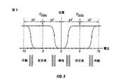
一実施例において、プロセッサ21は、アレイ制御器22と交信するように構成される。一実施例において、アレイ制御器22は、信号を画素30へ供給する行駆動回路24および列駆動回路26を含む。図1に示すアレイの断面図は図2の線1−1によって示される。MEMS干渉変調器に関しては、行/列作動プロトコルは、図3に示すこれらのデバイスのヒステリシス特性を利用することができる。例えば、可動層を解放状態から作動状態へ変形させるために10Vの電位差が必要である。しかし、電圧がその値から低下する場合、電圧が10V未満に落ちても、可動層はその状態を維持する。図3の代表的な実施例において、可動層は、電圧が2Vより低くなるまで完全には解放しない。その結果、デバイスが解放または作動状態のいずれかに安定する印加電圧の窓が存在する電圧範囲がある。図3に示す例においてはそれは約3から7Vである。これをここでは「ヒステリシス窓」または「安定窓」と呼ばれる。図3のヒステリシス特性を持っている表示アレイにおいて、行のストロービングの期間、ストローブされる行内の作動されるべき画素は約10Vの電圧差をかけられ、また解放されるべき画素は0Vに近い電圧差をかけられるように、行/列作動プロトコルが設計されることができる。ストローブの後は、画素は約5Vの定常状態電圧差をかけられ、その結果画素は、行ストローブによって置かれたいずれの状態にもとどまる。書き込まれた後、各画素には、この例では3から7Vの「安定窓」の中の電位差がかかっている。この特徴により、図1に示す画素設計は、同じ印加電圧条件のもとでも、前の作動または解放状態のいずれかに安定する。干渉変調器の各画素は、作動状態、解放状態を問わず、本質的には固定および可動反射器で形成されたキャパシタであるため、ヒステリシス窓内の電圧で、ほとんど電力消費せずに安定状態が保持される。本質的に、印加電圧が固定していれば画素への電流流入はない。 In one embodiment, the
典型的な用途において、表示フレームは、第1行内の作動される画素の所望の組に従って、列電極の組を宣言することにより作られることができる。行パルスは行1の電極に印加され、宣言された列線路に関連する画素を作動させる。次に列電極の宣言された組は第2行内の作動画素の所望の組に関連して変更される。次に、パルスが行2の電極に印加され、宣言された列電極に従って行2内の適切な画素を作動させる。行1の画素は行2パルスの影響を受けず、行1パルスの期間に設定された状態にとどまる。これは連続するすべての行に対して連続した方式で繰り返し、フレームを生成することができる。一般に、フレームは毎秒所望のフレーム数でこの過程を連続的に繰り返すことにより、リフレッシュおよび/または新しい表示データで更新される。表示フレームを形成するために画素アレイの行および列電極を駆動するための種々のプロトコルが知られており、本発明に関連して用いられることができる。 In a typical application, a display frame can be created by declaring a set of column electrodes according to the desired set of activated pixels in the first row. A row pulse is applied to the
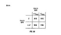
図4および図5に、図2の3×3のアレイに表示フレームを形成するための1つの可能性のある作動プロトコルを示す。図4に図3のヒステリシス曲線を示す画素に対して用いられる列および行電圧レベルの可能性のあるセットを示す。図4の実施例において、画素を作動させることは、適切な列を−Vbiasに、適切な行を+ΔVに設定することを含む。これらの値はそれぞれ−5Vおよび+5Vと一致することができる。画素を解放することは、適切な列を+Vbiasに、適切な行を同じ+ΔVに設定し、画素に0Vの電位差を与えることによって達成される。4 and 5 illustrate one possible actuation protocol for forming a display frame in the 3 × 3 array of FIG. FIG. 4 shows a possible set of column and row voltage levels used for the pixels showing the hysteresis curve of FIG. In the example of FIG. 4, actuating the pixels includes setting the appropriate column to -Vbias and the appropriate row to + ΔV. These values can be in agreement with -5V and + 5V, respectively. Releasing the pixel is accomplished by setting the appropriate column to + Vbias , the appropriate row to the same + ΔV, and giving the pixel a 0V potential difference.
行電圧が0Vに保持されている行においては、画素は初めにあった状態によらず、列が+Vbiasまたは−Vbiasにあるかに関係なく安定である。In a row where the row voltage is held at 0V, the pixel is stable regardless of whether it is in the original state, regardless of whether the column is at + Vbias or -Vbias .
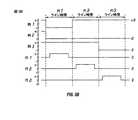
図5Bは、結果として図5Aに示す画素配置となるであろう図2の3×3のアレイに印加する一連の行および列信号を示すタイミング図である。ここで作動画素は非反射的とする。図5Aに示すフレームを書き込む前に、画素は任意の状態にあっても良い。この例ではすべての行は0Vにあり、すべての列+5Vにある。これらの印加電圧により、全画素は作動または解放の現在の状態に安定している。 FIG. 5B is a timing diagram showing a series of row and column signals applied to the 3 × 3 array of FIG. 2 that would result in the pixel arrangement shown in FIG. 5A. Here, the working pixel is assumed to be non-reflective. Prior to writing the frame shown in FIG. 5A, the pixels may be in any state. In this example, all rows are at 0V and all columns are at + 5V. With these applied voltages, all pixels are stable in the current state of operation or release.
図5Aのフレームにおいて、画素、(1,1)、(1,2)、(2,2)、(3,2)および(3,3)が作動される。これを達成するために、行1に対する「ライン時間」の期間、列1および列2は−5Vに設定され、列3は+5Vに設定される。すべての画素は3から7Vの安定窓内にとどまるため、どの画素の状態も変化しない。次に行1は0Vから5Vへ上昇し0Vへ戻るパルスでストローブされる。これは画素(1,1)および(1,2)作動させ、画素(1,3)を解放する。アレイの他の画素は影響を受けない。行2を所望のように設定するために、列2は−5Vに設定され、列1および列3は+5Vに設定される。行2に印加される同じストローブにより、画素(2,2)が作動し、画素(2,1)および(2,3)が解放されるだろう。同様に、アレイの他の画素は影響を受けない。行3は列2および列3を−5Vに、列1を+5Vに設定することにより同様に設定される。行3のストローブは行3の画素を図5Aに示すように設定する。フレームの書き込み後、行電位は0であり列電位は+5Vまたは−5Vのいずれかにとどまっていても良く、従って表示は図5Aの配置で安定している。同様の手順が数十または数百の行および列のアレイに対して用いられることが理解されるだろう。行および列の作動を実行するために用いられるタイミング、順序、および電圧レベルは上で概説した一般的原理の範囲内で広く変更可能であること、および上例は単に代表的にしか過ぎず、いかなる作動電圧方法も本発明と共に用いられることも理解されるだろう。例えば、行が6.2Vから6.2V+Vbiasになり、同様に列が例えば1Vから1V+2*Vbiasに切り替わるように、アレイ駆動回路の回路共通電圧からシフトとしている電圧でアレイ素子が駆動されることが理解されるだろう。この実施例において、解放電圧は0Vとは少し異なることができる。それは、2V程度でも良いが通常は1Vより低い。In the frame of FIG. 5A, the pixels (1,1), (1,2), (2,2), (3,2) and (3,3) are activated. To accomplish this, during the “line time” period for
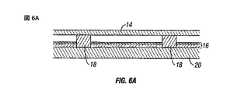
上述した原理に従って動作する干渉変調器の構造の細部は様々に変化することができる。例えば、図6A−6Cに可動反射板の3つの異なる実施例を示す。図6Aは図1の実施例の断面図であり、ストリップ状金属材料14が直交して伸びている支持物18上に堆積される。図6Bにおいて、可動反射材料14は支持物の角だけに係留体32で接続される。図6Cにおいて、可動反射材料14は変形可能層34から吊り下げられている。本実施例は利点を有しており、それは反射材料14に用いられる構造設計と材料を光特性に関して最適化でき、変形可能層34に用いるための構造設計および材料を所望の機械的特性に関して最適化できるためである。種々の形式の干渉デバイスの製造は、例えば米国特許出願2004/0051929を含む多くの刊行物に述べられている。一連の材料堆積、パターニングおよびエッチングステップを含む多くの周知の方法が上述した構造を製造するために用いられることができる。 The details of the structure of interferometric modulators that operate in accordance with the principles set forth above may vary. For example, FIGS. 6A-6C show three different embodiments of the movable reflector. FIG. 6A is a cross-sectional view of the embodiment of FIG. 1, in which a strip of
デバイスが作動され常に同じ方向の電界で作動状態に保持される場合に特に、デバイスの層間の誘電体に電荷が蓄積される場合があることは上述のデバイスの1つの性質である。例えば、デバイスが大きい方の安定しきい値よりも大きい電位で作動される時に、可動層が常に固定層に較べてより高い電位にあると、層間の誘電体上の緩やかに上昇する電荷蓄積によりデバイスのヒステリシス曲線がシフトし始めることがある。これは、時間と共に異なる様に作動される異なる画素に対して、時間と共におよびそれぞれ違う変化を生ずるため望ましくない。図5Bの例に見ることができるように、与えられた画素には、作動期間に、10Vの差があり、この例ではいつも行電極は列電極より電位が10V高い。それ故、作動期間はプレート間の電界は常に行電極から列電極の一方向に向いている。 It is one property of the device described above that charge may accumulate in the dielectric between the layers of the device, especially when the device is operated and always kept in an active state with an electric field in the same direction. For example, when the device is operated at a potential greater than the larger stability threshold, if the movable layer is always at a higher potential than the fixed layer, then the slowly rising charge accumulation on the dielectric between layers The device hysteresis curve may begin to shift. This is undesirable because it causes different changes over time and for different pixels that are operated differently over time. As can be seen in the example of FIG. 5B, for a given pixel, there is a difference of 10V in operating period, and in this example the row electrode is always 10V higher than the column electrode. Therefore, during the operation period, the electric field between the plates is always directed in one direction from the row electrode to the column electrode.
この問題は、MEMS表示素子を表示書き込み過程の第1の部分の期間は第1の極性の電位差で作動させ、MEMS表示素子を表示書き込み過程の第2の部分の期間は第1の極性とは逆の極性を持つ電位差で作動させることにより減少できる。図7、8A、および8Bにこの基本原理を示す。 The problem is that the MEMS display element is operated with a potential difference of the first polarity during the first part of the display writing process, and the first polarity is not used during the second part of the display writing process. It can be reduced by operating with a potential difference with the opposite polarity. Figures 7, 8A and 8B illustrate this basic principle.
図7において、表示データの2つのフレーム、フレームNおよびフレームN+1が連続して書き込まれる。この図において、列用のデータは、列1のライン時間の期間、列1に対して有効となり(すなわち、列1内の画素の所望状態に依存して+5または−5のいずれか)、列2のライン時間の期間、列2に対して有効となり、列3のライン時間の期間、列3に対して有効となる。フレームNは図5Bに示すように、MEMSデバイス作動の期間、列電極より10V高い行電極で書き込まれる。これをここで正極性と名付ける。作動の期間、列電極は−5Vであることができる。また、この例では行に関する走査電圧は+5Vである。このように、フレームNに対する作動および解放は図4と同じ図8Aの表に従って実行される。 In FIG. 7, two frames of display data, frame N and frame N + 1 are written successively. In this figure, the data for the column is valid for
フレームN+1は図8Bの表に従って書き込まれる。フレームN+1において、走査電圧は−5Vであり、列電圧は作動用に+5V、および解放用に−5Vに設定される。したがって、フレームN+1において列電圧は行電圧より10V高く、ここでは負極性と名付けられる。表示は連続的にリフレッシュおよび/または更新されるため、フレームN+2がフレームNと同じ方法で書き込まれ、フレームN+3がフレームN+1と同じ方法で書き込まれ、以下同様に、極性はフレーム間で交互に替わっても良い。このように、画素の作動は両方の極性で行われる。この原理に従う実施例において、逆極性の2つの電位は、定められた時刻に、画像データがアレイのMEMS素子に書き込まれる速度に依存する定められた持続時間、与えられたMEMS素子にそれぞれ印加される。また逆電位差は、表示に用いる与えられた期間にわたり、ほぼ等しい長さの時間、それぞれ印加される。これは、時間と共に増加する誘電体上の電荷蓄積を抑圧することに役立つ。 Frame N + 1 is written according to the table of FIG. 8B. In frame N + 1, the scan voltage is -5V and the column voltage is set to + 5V for operation and -5V for release. Therefore, in the frame N + 1, the column voltage is 10 V higher than the row voltage, and is named negative polarity here. Since the display is continuously refreshed and / or updated, frame N + 2 is written in the same manner as frame N, frame N + 3 is written in the same manner as frame N + 1, and so on, and the polarity alternates between frames. May be. Thus, pixel operation is performed in both polarities. In an embodiment according to this principle, two potentials of opposite polarity are applied to a given MEMS element, at a defined time, for a defined duration that depends on the rate at which image data is written to the MEMS elements of the array. The The reverse potential difference is applied for a substantially equal length of time over a given period used for display. This helps to suppress charge accumulation on the dielectric that increases with time.
この方式の種々の変更を実施することができる。例えば、フレームNおよびフレームN+1は、異なる表示データを含んでも良い。代替的に、それはアレイに逆特性で2回書き込まれる同じ表示データであっても良い。また、所望の表示データを書き込む前に、すべてのもしくは実質的にすべての画素の状態を解放状態に設定するために、および/または、すべてのもしくは実質的にすべての画素の状態を作動状態に設定するために、いくつかのフレームを提供することは有益である。一つの行のライン時間内に、例えばすべての列を+5V(または−5V)に設定し、すべての行を同時に−5V走査(または+5V走査)で走査することによって、すべての画素を共通状態に設定することが実行されても良い。 Various modifications of this scheme can be implemented. For example, the frame N and the frame N + 1 may include different display data. Alternatively, it may be the same display data that is written twice to the array with opposite characteristics. Also, prior to writing the desired display data, to set the state of all or substantially all pixels to a released state and / or to activate all or substantially all pixel states Providing several frames to set up is beneficial. Within a line time of one row, for example, by setting all columns to + 5V (or -5V) and scanning all rows simultaneously with a -5V scan (or + 5V scan), all pixels are brought into a common state. Setting may be performed.
そのような実施例の1つにおいて、所望の表示データが1つの極性でアレイに書き込まれ、全ての画素データが解放され、同じ表示データがもう一度逆極性で書き込まれる。これは、フレームN+1と同様のフレームNを持ち、またフレーム間に挿入されたアレイ解放ライン時間を持つ、図7に示す方式と同様である。他の実施例において、行解放ライン時間は新しい表示データの各表示更新に先行する。 In one such embodiment, the desired display data is written to the array with one polarity, all pixel data is released, and the same display data is once again written with the opposite polarity. This is similar to the scheme shown in FIG. 7 with frame N similar to frame N + 1 and with array release line time inserted between frames. In another embodiment, the line release line time precedes each display update of new display data.
他の実施例において、行ライン時間はアレイのすべての画素を作動させるために用いられ、第2のライン時間はアレイのすべての画素を解放するために用いられ、次に表示データ(例えばフレームN)が表示に書き込まれる。この実施例において、アレイ作動ライン時間、およびフレームNに先行する極性とは逆の極性のアレイ解放ライン時間がフレームN+1に先行しても良い。次に、フレームN+1が書き込まれても良い。いくつかの実施例において、1つの極性の作動ライン時間、同じ極性の解放ライン時間、逆極性の作動ライン時間、および逆極性の解放ライン時間はフレーム毎に先行しても良い。これらの実施例は、すべてまたは実質的にすべての画素が表示データの毎フレームに対して少なくとも一度作動することを確実にし、電荷蓄積の抑圧と同様に経時変化効果差を抑圧する。 In another embodiment, the row line time is used to activate all the pixels in the array, the second line time is used to release all the pixels in the array, and then display data (eg, frame N ) Is written to the display. In this embodiment, the array activation line time and the array release line time of the opposite polarity to the polarity preceding frame N may precede frame N + 1. Next, frame N + 1 may be written. In some embodiments, one polarity activation line time, the same polarity release line time, a reverse polarity activation line time, and a reverse polarity release line time may precede each frame. These embodiments ensure that all or substantially all pixels are activated at least once for each frame of display data, and suppress aging effect differences as well as suppression of charge accumulation.
いくつかの場合、アレイ作動ライン時間の期間、特別な高い作動電圧を用いることは有利である。例えば、上述したアレイ作動ライン時間の期間、行の走査電圧は5Vではなく7Vまたは10Vであっても良い。この実施例において、画素に印加される最高電圧は、表示データ更新期間ではなくこれらの「過剰作動」のアレイ作動時間の期間に発生する。いくつかの画素は表示される画像によって表示更新期間中に頻繁に変化することができるし、一方他の画素は表示更新期間中にほとんど変化しない。上記はそのような異なる画素に対する経事変化差を減少させることに役立つことができる。 In some cases, it is advantageous to use a special high operating voltage for the duration of the array operating line time. For example, the row scanning voltage may be 7V or 10V instead of 5V during the array operation line time period described above. In this embodiment, the highest voltage applied to the pixel occurs during these “over-actuated” array activation time periods rather than the display data update period. Some pixels can change frequently during the display update period depending on the image being displayed, while other pixels rarely change during the display update period. The above can help to reduce the time change difference for such different pixels.
また、行毎に、これらの極性反転および作動/解放プロトコルを実行することが可能である。これらの実施例において、フレームの各行はフレーム書き込み過程の期間、一回より多く書き込まれることができる。例えば、フレームNの行1を書き込む場合、行1の画素はすべて解放され、行1に対する表示データは正極性で書き込まれることができる。行1の画素はもう一度解放され、行1の表示データは負極性で再度書き込まれることができる。また、全体のアレイに対して上述したように、行1のすべての画素を作動させることが実行されることができる。さらに、解放、作動、および過剰作動が表示更新/リフレッシュ過程期間の毎行書き込みまたは毎フレーム書き込みより低い頻度で実行されることがさらに理解されるだろう。 It is also possible to perform these polarity reversal and activation / release protocols for each row. In these embodiments, each row of the frame can be written more than once during the frame writing process. For example, when writing
図9Aおよび9Bは、表示デバイス2040の実施例を示すシステムブロック図である。例えば、表示デバイス2040は、携帯電話または移動電話でも良い。しかし、表示デバイス2040またはそれのわずかに変形した同じ部品も、テレビジョンおよび携帯メディアプレーヤーのような種々の形式の表示デバイスの実例である。 FIGS. 9A and 9B are system block diagrams illustrating an embodiment of a
表示デバイス2040は筐体2041、表示器2030、アンテナ2043、スピーカ2045、入力デバイス2048、およびマイクロホン2046を含む。一般に、筐体2041は射出成形および真空成形を含む当業者に周知の種々の製造プロセスのいずれかで形成される。さらに、筐体2041は、プラスチック、金属、ガラス、ゴム、セラミック、またはそれらの組み合わせを非限定的に含む種々の材料のいずれかで作られることができる。一実施例において、筐体2041は可換部分(図示しない)を含む。これは異なる色の、または異なるロゴ、絵もしくはシンボルを含む他の可換部分と交換可能であることができる。 The
代表的な表示デバイス2040の表示器2030は、ここに述べるような双安定表示器を含む種々の表示器のいずれかであることができる。他の実施例において、表示器2030は、当業者に周知の、プラズマ、EL、OLED、STN LCD、もしくは上述のTFT LCDのような平面表示器、または、CRTもしくは他の真空管デバイスのような非平面表示器を含む。しかし、本実施例について説明するために、表示器2030はここに説明されるような干渉変調器表示器を含む。 The
代表的表示デバイス2040の一実施例の部品を図9Bに図式的に示す。例示した代表的表示デバイス2040は、筐体2041を含み、そこに少なくとも部分的に内蔵された付加コンポーネントを含んでも良い。例えば、一実施例において、代表的な表示デバイス2040は、送受信機2047に接続されたアンテナ2043を含むネットワークインタフェース2027を含む。送受信機2047はプロセッサ2021に接続され、プロセッサは調整用ハードウェア2052に接続される。調整用ハードウェア2052は、信号を調整(例えば信号をフィルタリングする)するように構成されることができる。調整用ハードウェア2052は、スピーカ2045およびマイクロホン2046に接続される。プロセッサ2021は、入力装置2048およびドライバ制御器2029にも接続される。ドライバ制御器2029は、フレームバッファ2028およびアレイドライバ2022に接続される。アレイドライバは次に表示アレイ2030に接続される。電源2050は特定の代表的な表示デバイス2040の設計が要求するようにすべての部品へ電力を供給する。 The components of one embodiment of
ネットワークインタフェース2027は、代表的表示デバイス2040がネットワーク上で1つ以上のデバイスと交信できるように、アンテナ2043および送受信機2047を含む。一実施例において、ネットワークインタフェース2027は、プロセッサ2021の要求事項を緩和するためのいくつかの処理能力を有することができる。アンテナ2043は信号を送信および受信するための当業者に周知の任意のアンテナである。一実施例において、アンテナは、IEEE802.11(a)、(b)、または(g)を含むIEEE802.11規格に従うRF信号を送信および受信する。他の実施例において、アンテナは、BLUETOOTH(登録商標)規格に従うRF信号を送信および受信する。携帯電話の場合において、アンテナは、CDMA、GSM(登録商標)、AMPS、または無線携帯電話ネットワーク内で交信するために用いられる他の周知の信号を受信するように設計される。信号をプロセッサ2021で受信し、さらに処理するために送受信機2047はアンテナ2043からの受信信号を前処理する。信号をアンテナ2043を介して代表的表示デバイス2040から送信するために、送受信機2047はプロセッサ2021からの受信信号も処理する。 The
代替的な実施例において、送受信機2047は受信機に置き換えても良い。さらに他の代替的な実施例において、ネットワークインタフェース2027は、プロセッサへ送られるべき画像データを蓄積または発生することができる画像源で置き替えても良い。例えば、画像源は、デジタルビデオディスク(DVD)、画像データを格納するハードディスクドライブ、または画像データを発生するソフトウェアモジュールであっても良い。 In an alternative embodiment, the
プロセッサ2021は、一般に代表的表示デバイス2040の全体的動作を制御する。プロセッサ2021は、ネットワークインタフェース2027または画像源から圧縮画像データのようなデータを受信し、データを生画像データへ、または生画像データへ容易に処理されるフォーマットへ加工する。プロセッサ2021は、次に処理済データをドライバ制御器2029または格納のためのフレームバッファ2028へ送る。通常、生データは画像内の各位置における画像の特性を特定する情報を指す。例えば、そのような画像特性は色、彩度、およびグレースケールレベルを含んでいても良い。 The
一実施例において、プロセッサ2021は、代表的表示デバイス2040の動作を制御するためのマイクロコントローラ、CPU、または論理演算装置を含む。一般に、調整ハードウェア2052は、スピーカ2045へ信号を送るための、およびマイクロホン2046から信号を受信するための増幅器およびフィルタを含む。調整ハードウェア2052は、代表的表示デバイス2040内の個別部品であるか、またはプロセッサ2021もしくは他の部品内に組み込まれることができる。 In one embodiment,
ドライバ制御器2029は、プロセッサ2021で生成された生画像データをプロセッサ2021から直接またはフレームバッファ2028からのいずれかで取り込み、生画像データをアレイドライバ2022への高速伝送用に適切に再フォーマットする。具体的には、ドライバ制御器2029は、表示アレイ2030全体にわたる走査に適した時間順序を有するように、生の画像データをラスタのようなフォーマットを有するデータフローへ再フォーマットする。次に、ドライバ制御器2029は、フォーマットされた情報をアレイドライバ2022に送る。LCD制御器のようなドライバ制御器2029はしばしば独立型集積回路(IC)としてシステムプロセッサ2021に関連しているが、そのような制御器は多くの方法で実施されることができる。それらは、ハードウェアとしてプロセッサ2021に埋め込まれ、ソフトウェアとしてプロセッサ2021に埋め込まれ、またはハードウェアとしてアレイドライバ2022と共に完全に集積化されることができる。 The
通常、アレイドライバ2022はドライバ制御器2029からフォーマットされた情報を受信し、映像データを波形の並列のセットへ再フォーマットする。この波形は表示画素のx−y行列から出ている数百、時には数千のリード線へ毎秒多数回印加される。 Typically, the
一実施例において、ドライバ制御器2029、アレイドライバ2022、および表示アレイ2030はここに説明されたいずれの形式の表示器に対しても適切である。例えば、一実施例において、ドライバ制御器2029は、従来の表示制御装置または双安定表示制御器(例えば干渉変調器制御器)である。他の実施例において、アレイドライバ2022は、従来のドライバまたは双安定表示ドライバ(例えば、干渉変調器型表示)である。一実施例において、ドライバ制御器2029はアレイドライバ2022と集積化される。そのような実施例は、携帯電話、腕時計、他の小面積表示器などの高集積度システムにおいて一般的である。さらに他の実施例において、表示アレイ2030は、通常の表示アレイまたは双安定表示アレイ(例えば、干渉変調器アレイを含む表示器)である。 In one embodiment,
入力デバイス2048により、ユーザは代表的な表示デバイス2040の動作を制御できる。一実施例において、入力デバイス2048はQWERTYキーボードまたは電話キーパッドのようなキーパッド、ボタン、スイッチ、接触式スクリーン、圧力もしくは感熱膜を含む。一実施例において、マイクロホン2046は代表的表示デバイス2040のための入力デバイスである。マイクロホン2046がデータをデバイスに入力するために用いられる場合、音声コマンドが代表的表示デバイス2040の動作を制御するためにユーザによって与えられることができる。
電源2050は、当業者に周知の種々のエネルギー蓄積デバイスを含んでもよい。例えば、一実施例において、電源2050はニッケルカドミウム電池またはリチウムイオン電池のような二次電池である。他の実施例において、電源2050は、再生可能エネルギー源、コンデンサ、またはプラスチック太陽電池を含む太陽電池、および太陽電池塗料である。他の実施例において、電源2050は、壁コンセントから電力を受けるように構成される。 The
いくつかの実施において、制御プログラム化能力は、上述したように、電子表示システム内のいくつかの場所にあるドライバ制御器内にある。いくつかの場合、制御プログラム化能力はアレイドライバ2022にある。当業者は、上で説明された最適化が多くのハードウェア並びに/またはソフトウェア部品、および種々の構成で実施されることを理解するだろう。 In some implementations, the control programming capability is in a driver controller at several locations within the electronic display system, as described above. In some cases, the control programming capability resides in the
上の詳細な説明は種々の実施例に適用される場合の本発明の新しい特徴を示し、説明し、指摘したが、例示したデバイスまたはプロセスの形式並びに詳細における種々の省略、置き換え、および変更は、本発明の精神から逸脱することなく当業者によってなされることが理解されるだろう。一例として、試験電圧駆動回路が、表示生成のために用いられるアレイ駆動回路から独立していることが理解されるだろう。電流センサと同様に、別々の電圧センサが、別々の行電極に専用に用いられることができる。本発明の範囲は以上の記述によるよりもむしろ添付した請求範囲により示される。請求範囲の均等性の意味および範囲内に生ずるすべての変更は請求範囲の範囲内に包含されるべきものである。 While the above detailed description illustrates, describes, and points out new features of the present invention as applied to various embodiments, various omissions, substitutions, and changes in the form and details of the illustrated device or process are not intended. It will be understood that this can be done by those skilled in the art without departing from the spirit of the invention. As an example, it will be appreciated that the test voltage driver circuit is independent of the array driver circuit used for display generation. Similar to current sensors, separate voltage sensors can be dedicated to separate row electrodes. The scope of the invention is indicated by the appended claims rather than by the foregoing description. All changes that come within the meaning and range of equivalency of the claims are to be embraced within their scope.
Claims (98)
Translated fromJapanese表示書き込み過程の第1の部分の期間に、第1の極性の電位差で、MEMS表示素子を作動させる駆動回路を制御するように構成された制御器であって、前記作動後に駆動回路に前記MEMS表示素子を解放させ、次に前記表示書き込み過程の第2の部分の期間に前記第1の極性と逆の極性の電位差で前記MEMS表示素子を作動させるように構成されている制御器と、
表示書き込み過程の前記第1の部分の期間に、電位差をMEMS表示素子に少なくとも部分的に伝達するように構成された少なくとも1つの出力端子とを含む装置。An apparatus configured to drive a MEMS display element, comprising:
A controller configured to control a drive circuit that operates a MEMS display element with a potential difference of a first polarity during a first portion of a display writing process, wherein the MEMS is connected to the drive circuit after the operation. A controller configured to release the display element and then operate the MEMS display element with a potential difference of a polarity opposite to the first polarity during a second portion of the display writing process;
And at least one output terminal configured to at least partially transmit a potential difference to the MEMS display element during the first portion of the display writing process.
前記MEMS表示素子を作動させるために表示データの第1のフレームを前記第1の極性の電位差でMEMS表示素子アレイに書き込み、
前記アレイ内の実質的にすべてのMEMS素子を解放状態におき、
かつ、前記MEMS表示素子を作動させるために表示データの第2のフレームを前記第1の極性と逆の極性の電位差で前記アレイに書き込むように構成された請求項1に記載の装置。The controller is
Writing a first frame of display data to the MEMS display element array with a potential difference of the first polarity to activate the MEMS display element;
Leaving substantially all MEMS elements in the array open;
2. The apparatus of claim 1, wherein the apparatus is configured to write a second frame of display data to the array with a potential difference of a polarity opposite to the first polarity to activate the MEMS display element.
前記プロセッサと電気的に交信しているメモリデバイスとをさらに含む請求項1に記載の装置。A processor in electrical communication with the MEMS display element, the processor configured to process image data;
The apparatus of claim 1, further comprising a memory device in electrical communication with the processor.
MEMS表示素子アレイの行内の実質的にすべてのMEMS素子を解放状態に置き、
前記MEMS表示素子を作動させるために表示データの第1の組を前記第1の極性の電位差で行に書き込み、
前記行内の実質的にすべてのMEMS素子を解放状態に置き、
かつ、前記MEMS表示素子を作動させるために表示データの第2の組を前記第1の極性とは逆の極性の電位差で前記行に書き込むように構成された請求項1に記載の装置。The controller is
Placing substantially all MEMS elements in a row of the MEMS display element array in a free state;
Writing a first set of display data in a row with a potential difference of the first polarity to operate the MEMS display element;
Placing substantially all MEMS elements in the row in a released state;
The apparatus of claim 1, wherein the apparatus is configured to write a second set of display data to the row with a potential difference opposite in polarity to the first polarity in order to operate the MEMS display element.
表示書き込み過程の第1の部分の期間に、第1の極性の電位差で、前記MEMS表示素子の作動を制御するため、および前記MEMS表示素子を解放させ次に表示書き込み過程の第2の部分の期間に前記第1の極性と逆の極性を有する電位差で前記MEMS表示素子の作動を制御するための手段と、
前記表示書き込み過程の第1の部分の期間に、電位差を前記MEMS表示素子に少なくとも部分的に伝達するための手段とを含む装置。An apparatus configured to drive a set of MEMS display elements,
During the first part of the display writing process, the potential difference of the first polarity is used to control the operation of the MEMS display element and to release the MEMS display element and then to the second part of the display writing process. Means for controlling operation of the MEMS display element with a potential difference having a polarity opposite to the first polarity in a period;
Means for at least partially transmitting a potential difference to the MEMS display element during a first portion of the display writing process.
前記MEMS表示素子の作動を制御することによって表示データの第1のフレームを前記第1の極性の電位差でMEMS表示素子の前記組に書き込み、
前記組内の実質的にすべてのMEMS素子を解放状態におき、
かつ、前記MEMS表示素子の作動を制御することによって表示データの第2のフレームを前記第1の極性と逆の極性の電位差で先記組に書き込むようにさらに構成された請求項21に記載の装置。The device is
Writing a first frame of display data to the set of MEMS display elements with a potential difference of the first polarity by controlling the operation of the MEMS display element;
Leaving substantially all MEMS elements in the set open;
24. The apparatus according to claim 21, further configured to write a second frame of display data to the preceding set with a potential difference opposite to the first polarity by controlling operation of the MEMS display element. apparatus.
前記組の行内の実質的にすべてのMEMS素子を解放状態に置き、
前記MEMS表示素子の作動を制御することによって表示データの第1の組を前記第1の極性の電位差で前記組の前記行に書き込み、
前記組の前記行内の実質的にすべてのMEMS素子を解放状態に置き、
かつ、前記MEMS表示素子の作動を制御することによって表示データの第2の組を前記第1の極性と逆の極性の電位差で前記組の前記行に書き込むように構成された請求項21に記載の装置。The device is
Placing substantially all MEMS elements in the set of rows in an open state;
Writing a first set of display data to the rows of the set with a potential difference of the first polarity by controlling the operation of the MEMS display element;
Placing substantially all MEMS elements in the row of the set in a released state;
And wherein the second set of display data is written to the row of the set with a potential difference of a polarity opposite to the first polarity by controlling operation of the MEMS display element. Equipment.
表示書き込み過程の第1の部分の期間に第1の極性の電位差で前記MEMS表示素子を作動させることと、
前記MEMS表示素子を解放することと、
前記表示書き込み過程の第2の部分の期間に前記第1の極性とは逆の極性を有する電位差で前記MEMS表示素子を作動させることとを含む方法。A method of operating a set of MEMS display elements including a portion of a MEMS display element array comprising:
Activating the MEMS display element with a potential difference of a first polarity during a first portion of a display writing process;
Releasing the MEMS display element;
Operating the MEMS display element with a potential difference having a polarity opposite to the first polarity during a second portion of the display writing process.
前記MEMS表示素子を作動させるために表示データの第1の組を前記第1の極性の電位差で前記アレイの前記行に書き込むことと、
前記アレイの前記行内の実質的にすべてのMEMS素子を解放状態におくことと、
前記MEMS表示素子を作動させるために表示データの第2の組を前記第1の極性とは逆の極性の電位差で前記アレイの前記行に書き込むこととをさらに含む請求項40に記載の方法。Placing substantially all MEMS elements in a row of the array in a released state;
Writing a first set of display data to the rows of the array with a potential difference of the first polarity to operate the MEMS display element;
Leaving substantially all MEMS elements in the row of the array open;
41. The method of claim 40, further comprising writing a second set of display data to the row of the array with a potential difference opposite to the first polarity to operate the MEMS display element.
前記アレイ内の実質的にすべてのMEMS素子を解放状態におくことと、
前記MEMS表示素子を作動させるために表示データの第2のフレームを前記第1の極性とは逆の極性の電位差で前記アレイに書き込むこととをさらに含む請求項40に記載の方法。Writing a first frame of display data to the array with a potential difference of the first polarity to activate the MEMS display element;
Leaving substantially all MEMS elements in the array open;
41. The method of claim 40, further comprising writing a second frame of display data to the array with a potential difference opposite to the first polarity to activate the MEMS display element.
前記MEMS素子を作動させるために十分な振幅を有し、かつ極性を有する第1の電位差を前記MEMS素子に周期的に印加する駆動回路を制御するように構成された制御器であって、前記第1の電位差とほぼ等しい振幅と逆極性の第2の電位差を前記MEMS素子に周期的に印加するように構成されており、前記第1の電位差および前記第2の電位差が定められた時刻、および画像データが前記アレイのMEMS素子に書き込まれるレートに依存する定められた継続時間にわたってMEMS素子にそれぞれ印加され、かつ前記第1および第2の電位差が表示用に定められた期間にわたり、それぞれほぼ等しい時間長、前記MEMS素子に印加され、前記第1の極性の電位差および前記第1の極性と逆の電位差の双方を用いて同じデータのフレームを書き込むようにさらに構成される、制御器と、
表示書き込み過程の第1の部分の期間に、電位差をMEMS表示素子に少なくとも部分的に伝達するように構成された少なくとも1つの出力端子とを含む装置。An apparatus configured to manipulate MEMS elements in a MEMS element array that forms a display comprising:
A controller configured to control a drive circuit that periodically applies a first potential difference having a sufficient amplitude and polarity to operate the MEMS element to the MEMS element, the controller comprising: A second potential difference having substantially the same amplitude and opposite polarity as the first potential difference is periodically applied to the MEMS element, and the time when the first potential difference and the second potential difference are determined; And image data is applied to the MEMS element for a defined duration that depends on the rate at which the data is written to the MEMS elements of the array, respectively, and the first and second potential differences are approximately over a defined period for display, respectively. An equal time length is applied to the MEMS element, and the same data frame is generated using both the potential difference of the first polarity and the potential difference opposite to the first polarity. Further configured to write over beam, a controller,
An apparatus comprising: at least one output terminal configured to at least partially transmit a potential difference to a MEMS display element during a first portion of a display writing process.
前記プロセッサと電気的に交信しているメモリデバイスとをさらに含む請求項51に記載の装置。A processor in electrical communication with the MEMS device, the processor configured to process image data;
52. The apparatus of claim 51, further comprising a memory device in electrical communication with the processor.
前記変調手段へ電位差を印加するための手段であって、前記印加手段は、第1の電位差および第2の電位差を前記変調手段に周期的に印加するように構成され、前記第1および第2の電位差は、前記変調手段を作動させるために十分な、逆極性でほぼ等しい振幅を有し、前記第1の電位差および前記第2の電位差が定められた時刻、および画像データが変調手段に書き込まれるレートに依存する定められた継続時間にわたって前記変調手段にそれぞれ印加され、かつ前記第1および第2の電位差が表示用に定められた期間にわたり、それぞれほぼ等しい時間長、前記変調手段に印加され、前記印加手段が、前記第1の極性の電位差および前記第1の極性とは逆の極性の電位差双方を用いて同じデータのフレームを書き込むようにさらに構成される手段とを含む表示を更新するための装置。Means for modulating the light;
A means for applying a potential difference to the modulating means, wherein the applying means is configured to periodically apply a first potential difference and a second potential difference to the modulating means, and the first and second The potential difference between the first potential difference and the second potential difference is sufficient to operate the modulation means, and has a substantially equal amplitude with the opposite polarity, and the image data is written to the modulation means. Applied to the modulating means for a predetermined duration depending on the rate to be applied, and the first and second potential differences are respectively applied to the modulating means for approximately equal time lengths over a period determined for display. The applying means is further configured to write the same frame of data using both the potential difference of the first polarity and the potential difference of the opposite polarity to the first polarity. Apparatus for updating a display including a that means.
前記MEMS素子を作動させるために十分な振幅を有し、かつ極性を有する第1の電位差を前記MEMS素子に周期的に印加することと、
前記第1の電位差とほぼ等しい振幅並びに逆極性である第2の電位差を、前記MEMS素子に周期的に印加することとを含み、
前記第1の電位差および前記第2の電位差が、定められた時刻、および画像データが前記アレイのMEMS素子に書き込まれるレートに依存する定められた継続時間にわたってMEMS素子にそれぞれ印加され、かつ前記第1および第2の電位差が表示用に定められた期間にわたり、それぞれほぼ等しい時間長、前記MEMS素子に印加され、
前記方法が、前記第1の電位差および前記第1の極性とは逆の電位差の双方を用いて同じデータのフレームを書き込むことを含む、
方法。A method for operating a MEMS element in a MEMS element array forming a display device, comprising:
Periodically applying a first potential difference having a sufficient amplitude and polarity to operate the MEMS element to the MEMS element;
Periodically applying to the MEMS element a second potential difference having an amplitude substantially equal to the first potential difference and a reverse polarity;
The first potential difference and the second potential difference are respectively applied to the MEMS elements for a defined time and a defined duration that depends on a rate at which image data is written to the MEMS elements of the array; and A first and a second potential difference are applied to the MEMS element for approximately equal time lengths over a period determined for display,
The method includes writing a frame of the same data using both the first potential difference and a potential difference opposite to the first polarity.
Method.
前記表示の一部にあるすべてのMEMS素子を作動させ、かつ前記部分に表示データを書き込むように構成された制御器とを含む画像表示のための装置。An apparatus for image display comprising a plurality of MEMS elements in a display and a controller configured to activate all MEMS elements in a portion of the display and to write display data to the portion.
前記プロセッサと電気的に交信しているメモリデバイスとをさらに含む請求項69に記載の装置。A processor in electrical communication with at least one of the plurality of MEMS elements, wherein the processor is configured to process image data;
70. The apparatus of claim 69, further comprising a memory device in electrical communication with the processor.
光変調のため、および表示の一部に表示データを書き込むための前記複数の手段の作動を制御するための手段とを含む画像表示のための装置。A plurality of means for light modulation;
Means for image display including light modulation and means for controlling operation of the plurality of means for writing display data to a portion of the display.
前記アレイの一部内のすべてのMEMS素子を作動させることと、
前記アレイの前記部分に表示データを書き込むこととを含む方法。A method of writing display data to a MEMS display element array,
Activating all MEMS elements in a portion of the array;
Writing display data to the portion of the array.
列ドライバと、
行ドライバとを含み、
前記行ドライバおよび列ドライバが、第1および第2の電位差で前記アレイの少なくともいくつかの素子を作動させるように構成され、第2の電位差の絶対値が第1の電位差の絶対値より大きいシステム。A system configured to write data to a MEMS display element array comprising:
A column driver;
Line driver and
A system wherein the row and column drivers are configured to operate at least some elements of the array with first and second potential differences, wherein the absolute value of the second potential difference is greater than the absolute value of the first potential difference .
前記プロセッサと電気的に交信しているメモリデバイスとをさらに含む請求項89に記載のシステム。A processor in electrical communication with the array of MEMS display elements, the processor configured to process image data;
90. The system of claim 89, further comprising a memory device in electrical communication with the processor.
前記MEMS表示素子の列を駆動するための手段と、
前記MEMS表示素子の行を駆動するための手段とを含み、
前記行および列駆動手段が、第1および第2の電位差で前記アレイの少なくともいくつかの素子を作動させるように構成され、第2の電位差の絶対値が第1の電位差の絶対値より大きいシステム。A system configured to write data to a MEMS display element array comprising:
Means for driving a column of said MEMS display elements;
Means for driving a row of said MEMS display elements,
A system wherein the row and column driving means are arranged to operate at least some elements of the array with first and second potential differences, the absolute value of the second potential difference being greater than the absolute value of the first potential difference .
Applications Claiming Priority (6)
| Application Number | Priority Date | Filing Date | Title |
|---|---|---|---|
| US60489604P | 2004-08-27 | 2004-08-27 | |
| US60/604,896 | 2004-08-27 | ||
| US60622304P | 2004-08-31 | 2004-08-31 | |
| US60/606,223 | 2004-08-31 | ||
| US11/159,073 | 2005-02-25 | ||
| US11/159,073US7560299B2 (en) | 2004-08-27 | 2005-02-25 | Systems and methods of actuating MEMS display elements |
Related Parent Applications (1)
| Application Number | Title | Priority Date | Filing Date |
|---|---|---|---|
| JP2012023350ADivisionJP2012159842A (en) | 2004-08-27 | 2012-02-06 | Systems and methods of actuating mems display elements |
Publications (2)
| Publication Number | Publication Date |
|---|---|
| JP2014194539Atrue JP2014194539A (en) | 2014-10-09 |
| JP2014194539A5 JP2014194539A5 (en) | 2015-01-15 |
Family
ID=35502629
Family Applications (4)
| Application Number | Title | Priority Date | Filing Date |
|---|---|---|---|
| JP2007530007APendingJP2008511867A (en) | 2004-08-27 | 2005-08-23 | MEMS display element driving system and method |
| JP2011176877APendingJP2012022326A (en) | 2004-08-27 | 2011-08-12 | System and method of actuating mems display element |
| JP2012023350APendingJP2012159842A (en) | 2004-08-27 | 2012-02-06 | Systems and methods of actuating mems display elements |
| JP2014033249APendingJP2014194539A (en) | 2004-08-27 | 2014-02-24 | Systems and methods of actuating mems display elements |
Family Applications Before (3)
| Application Number | Title | Priority Date | Filing Date |
|---|---|---|---|
| JP2007530007APendingJP2008511867A (en) | 2004-08-27 | 2005-08-23 | MEMS display element driving system and method |
| JP2011176877APendingJP2012022326A (en) | 2004-08-27 | 2011-08-12 | System and method of actuating mems display element |
| JP2012023350APendingJP2012159842A (en) | 2004-08-27 | 2012-02-06 | Systems and methods of actuating mems display elements |
Country Status (13)
| Country | Link |
|---|---|
| US (2) | US7560299B2 (en) |
| EP (4) | EP2383725A1 (en) |
| JP (4) | JP2008511867A (en) |
| KR (1) | KR101222096B1 (en) |
| CN (1) | CN101887693A (en) |
| AU (1) | AU2005280270A1 (en) |
| BR (1) | BRPI0514646A (en) |
| CA (1) | CA2578029A1 (en) |
| IL (1) | IL181133A0 (en) |
| MX (1) | MX2007002211A (en) |
| SG (1) | SG156677A1 (en) |
| TW (1) | TWI353337B (en) |
| WO (1) | WO2006026226A2 (en) |
Families Citing this family (68)
| Publication number | Priority date | Publication date | Assignee | Title |
|---|---|---|---|---|
| US7471444B2 (en)* | 1996-12-19 | 2008-12-30 | Idc, Llc | Interferometric modulation of radiation |
| US8928967B2 (en) | 1998-04-08 | 2015-01-06 | Qualcomm Mems Technologies, Inc. | Method and device for modulating light |
| WO1999052006A2 (en) | 1998-04-08 | 1999-10-14 | Etalon, Inc. | Interferometric modulation of radiation |
| US7085059B2 (en)* | 2004-03-24 | 2006-08-01 | Silicon Light Machines Corporation | Spatial light modulator with robust mirror substrate condition |
| US7499208B2 (en)* | 2004-08-27 | 2009-03-03 | Udc, Llc | Current mode display driver circuit realization feature |
| US7889163B2 (en)* | 2004-08-27 | 2011-02-15 | Qualcomm Mems Technologies, Inc. | Drive method for MEMS devices |
| US7515147B2 (en)* | 2004-08-27 | 2009-04-07 | Idc, Llc | Staggered column drive circuit systems and methods |
| US7551159B2 (en)* | 2004-08-27 | 2009-06-23 | Idc, Llc | System and method of sensing actuation and release voltages of an interferometric modulator |
| US7560299B2 (en)* | 2004-08-27 | 2009-07-14 | Idc, Llc | Systems and methods of actuating MEMS display elements |
| US7602375B2 (en)* | 2004-09-27 | 2009-10-13 | Idc, Llc | Method and system for writing data to MEMS display elements |
| US7626581B2 (en)* | 2004-09-27 | 2009-12-01 | Idc, Llc | Device and method for display memory using manipulation of mechanical response |
| AU2005289445A1 (en) | 2004-09-27 | 2006-04-06 | Idc, Llc | Method and device for multistate interferometric light modulation |
| US8878825B2 (en) | 2004-09-27 | 2014-11-04 | Qualcomm Mems Technologies, Inc. | System and method for providing a variable refresh rate of an interferometric modulator display |
| US7843410B2 (en)* | 2004-09-27 | 2010-11-30 | Qualcomm Mems Technologies, Inc. | Method and device for electrically programmable display |
| US7724993B2 (en)* | 2004-09-27 | 2010-05-25 | Qualcomm Mems Technologies, Inc. | MEMS switches with deforming membranes |
| US8514169B2 (en) | 2004-09-27 | 2013-08-20 | Qualcomm Mems Technologies, Inc. | Apparatus and system for writing data to electromechanical display elements |
| US8310441B2 (en) | 2004-09-27 | 2012-11-13 | Qualcomm Mems Technologies, Inc. | Method and system for writing data to MEMS display elements |
| US7675669B2 (en)* | 2004-09-27 | 2010-03-09 | Qualcomm Mems Technologies, Inc. | Method and system for driving interferometric modulators |
| US7679627B2 (en)* | 2004-09-27 | 2010-03-16 | Qualcomm Mems Technologies, Inc. | Controller and driver features for bi-stable display |
| US7446927B2 (en)* | 2004-09-27 | 2008-11-04 | Idc, Llc | MEMS switch with set and latch electrodes |
| US7310179B2 (en)* | 2004-09-27 | 2007-12-18 | Idc, Llc | Method and device for selective adjustment of hysteresis window |
| US7136213B2 (en)* | 2004-09-27 | 2006-11-14 | Idc, Llc | Interferometric modulators having charge persistence |
| US7532195B2 (en)* | 2004-09-27 | 2009-05-12 | Idc, Llc | Method and system for reducing power consumption in a display |
| US7345805B2 (en)* | 2004-09-27 | 2008-03-18 | Idc, Llc | Interferometric modulator array with integrated MEMS electrical switches |
| US7545550B2 (en)* | 2004-09-27 | 2009-06-09 | Idc, Llc | Systems and methods of actuating MEMS display elements |
| US20060066594A1 (en)* | 2004-09-27 | 2006-03-30 | Karen Tyger | Systems and methods for driving a bi-stable display element |
| US7948457B2 (en)* | 2005-05-05 | 2011-05-24 | Qualcomm Mems Technologies, Inc. | Systems and methods of actuating MEMS display elements |
| EP1878001A1 (en)* | 2005-05-05 | 2008-01-16 | QUALCOMM Incorporated, Inc. | Dynamic driver ic and display panel configuration |
| US7920136B2 (en) | 2005-05-05 | 2011-04-05 | Qualcomm Mems Technologies, Inc. | System and method of driving a MEMS display device |
| US7355779B2 (en)* | 2005-09-02 | 2008-04-08 | Idc, Llc | Method and system for driving MEMS display elements |
| US20070126673A1 (en)* | 2005-12-07 | 2007-06-07 | Kostadin Djordjev | Method and system for writing data to MEMS display elements |
| US8391630B2 (en) | 2005-12-22 | 2013-03-05 | Qualcomm Mems Technologies, Inc. | System and method for power reduction when decompressing video streams for interferometric modulator displays |
| US7916980B2 (en) | 2006-01-13 | 2011-03-29 | Qualcomm Mems Technologies, Inc. | Interconnect structure for MEMS device |
| US8194056B2 (en)* | 2006-02-09 | 2012-06-05 | Qualcomm Mems Technologies Inc. | Method and system for writing data to MEMS display elements |
| US8049713B2 (en)* | 2006-04-24 | 2011-11-01 | Qualcomm Mems Technologies, Inc. | Power consumption optimized display update |
| US7957589B2 (en)* | 2007-01-25 | 2011-06-07 | Qualcomm Mems Technologies, Inc. | Arbitrary power function using logarithm lookup table |
| EP2067841A1 (en)* | 2007-12-06 | 2009-06-10 | Agfa HealthCare NV | X-Ray imaging photostimulable phosphor screen or panel. |
| US20090201282A1 (en)* | 2008-02-11 | 2009-08-13 | Qualcomm Mems Technologies, Inc | Methods of tuning interferometric modulator displays |
| US8466858B2 (en) | 2008-02-11 | 2013-06-18 | Qualcomm Mems Technologies, Inc. | Sensing to determine pixel state in a passively addressed display array |
| US8405649B2 (en)* | 2009-03-27 | 2013-03-26 | Qualcomm Mems Technologies, Inc. | Low voltage driver scheme for interferometric modulators |
| US8736590B2 (en) | 2009-03-27 | 2014-05-27 | Qualcomm Mems Technologies, Inc. | Low voltage driver scheme for interferometric modulators |
| US7990604B2 (en) | 2009-06-15 | 2011-08-02 | Qualcomm Mems Technologies, Inc. | Analog interferometric modulator |
| US20110109615A1 (en)* | 2009-11-12 | 2011-05-12 | Qualcomm Mems Technologies, Inc. | Energy saving driving sequence for a display |
| US9090456B2 (en)* | 2009-11-16 | 2015-07-28 | Qualcomm Mems Technologies, Inc. | System and method of manufacturing an electromechanical device by printing raised conductive contours |
| JP5310529B2 (en)* | 2009-12-22 | 2013-10-09 | 株式会社豊田中央研究所 | Oscillator for plate member |
| US20110164068A1 (en)* | 2010-01-06 | 2011-07-07 | Qualcomm Mems Technologies, Inc. | Reordering display line updates |
| US8310421B2 (en)* | 2010-01-06 | 2012-11-13 | Qualcomm Mems Technologies, Inc. | Display drive switch configuration |
| US20110164027A1 (en)* | 2010-01-06 | 2011-07-07 | Qualcomm Mems Technologies, Inc. | Method of detecting change in display data |
| US8884940B2 (en)* | 2010-01-06 | 2014-11-11 | Qualcomm Mems Technologies, Inc. | Charge pump for producing display driver output |
| WO2011112861A1 (en)* | 2010-03-12 | 2011-09-15 | Qualcomm Mems Technologies, Inc. | Line multiplying to enable increased refresh rate of a display |
| US8659611B2 (en)* | 2010-03-17 | 2014-02-25 | Qualcomm Mems Technologies, Inc. | System and method for frame buffer storage and retrieval in alternating orientations |
| EP2558893A4 (en) | 2010-04-16 | 2014-06-11 | Flex Lighting Ii Llc | TEACH COMPRISING A LIGHT GUIDE BASED ON A FILM |
| MX2012012033A (en) | 2010-04-16 | 2013-05-20 | Flex Lighting Ii Llc | Illumination device comprising a film-based lightguide. |
| US8294184B2 (en) | 2011-02-23 | 2012-10-23 | Qualcomm Mems Technologies, Inc. | EMS tunable transistor |
| US8780104B2 (en) | 2011-03-15 | 2014-07-15 | Qualcomm Mems Technologies, Inc. | System and method of updating drive scheme voltages |
| US8345030B2 (en) | 2011-03-18 | 2013-01-01 | Qualcomm Mems Technologies, Inc. | System and method for providing positive and negative voltages from a single inductor |
| US9239457B2 (en) | 2011-07-15 | 2016-01-19 | Pixtronix, Inc. | Circuits for controlling display apparatus |
| US8988409B2 (en) | 2011-07-22 | 2015-03-24 | Qualcomm Mems Technologies, Inc. | Methods and devices for voltage reduction for active matrix displays using variability of pixel device capacitance |
| US8786592B2 (en) | 2011-10-13 | 2014-07-22 | Qualcomm Mems Technologies, Inc. | Methods and systems for energy recovery in a display |
| US8836681B2 (en) | 2011-10-21 | 2014-09-16 | Qualcomm Mems Technologies, Inc. | Method and device for reducing effect of polarity inversion in driving display |
| US8847862B2 (en) | 2011-11-29 | 2014-09-30 | Qualcomm Mems Technologies, Inc. | Systems, devices, and methods for driving an interferometric modulator |
| US8669926B2 (en)* | 2011-11-30 | 2014-03-11 | Qualcomm Mems Technologies, Inc. | Drive scheme for a display |
| US9030391B2 (en) | 2011-11-30 | 2015-05-12 | Qualcomm Mems Technologies, Inc. | Systems, devices, and methods for driving an analog interferometric modulator |
| US9135843B2 (en) | 2012-05-31 | 2015-09-15 | Qualcomm Mems Technologies, Inc. | Charge pump for producing display driver output |
| US9305497B2 (en) | 2012-08-31 | 2016-04-05 | Qualcomm Mems Technologies, Inc. | Systems, devices, and methods for driving an analog interferometric modulator |
| US9195051B2 (en) | 2013-03-15 | 2015-11-24 | Pixtronix, Inc. | Multi-state shutter assembly for use in an electronic display |
| US10411958B2 (en)* | 2014-09-08 | 2019-09-10 | Intel Corporation | Automatic device configuration |
| KR102612038B1 (en)* | 2015-12-31 | 2023-12-07 | 엘지디스플레이 주식회사 | Liquid crystal display and method of driving the same |
Citations (6)
| Publication number | Priority date | Publication date | Assignee | Title |
|---|---|---|---|---|
| JPH02173724A (en)* | 1988-12-27 | 1990-07-05 | Nippondenso Co Ltd | Matrix type ferroelectric liquid crystal display device |
| JPH04311922A (en)* | 1991-04-11 | 1992-11-04 | Seiko Epson Corp | Driving method of liquid crystal electro-optical element |
| JPH06202082A (en)* | 1992-12-28 | 1994-07-22 | Citizen Watch Co Ltd | Driving method for antiferroelectric liquid crystal display |
| JP2000121970A (en)* | 1998-10-16 | 2000-04-28 | Fuji Photo Film Co Ltd | Array type optical modulation element and method for driving plane display |
| JP2002341267A (en)* | 2001-05-11 | 2002-11-27 | Sony Corp | Driving method for optical multi-layered structure, driving method for display device, and display device |
| JP2004534280A (en)* | 2001-07-10 | 2004-11-11 | イリディグム ディスプレイ コーポレイション | Photonic MEMS and structure |
Family Cites Families (329)
| Publication number | Priority date | Publication date | Assignee | Title |
|---|---|---|---|---|
| US577116A (en)* | 1897-02-16 | Divider for mowing-machines | ||
| US3982239A (en) | 1973-02-07 | 1976-09-21 | North Hills Electronics, Inc. | Saturation drive arrangements for optically bistable displays |
| NL8001281A (en) | 1980-03-04 | 1981-10-01 | Philips Nv | DISPLAY DEVICE. |
| US4441791A (en)* | 1980-09-02 | 1984-04-10 | Texas Instruments Incorporated | Deformable mirror light modulator |
| NL8103377A (en) | 1981-07-16 | 1983-02-16 | Philips Nv | DISPLAY DEVICE. |
| US4571603A (en)* | 1981-11-03 | 1986-02-18 | Texas Instruments Incorporated | Deformable mirror electrostatic printer |
| NL8200354A (en) | 1982-02-01 | 1983-09-01 | Philips Nv | PASSIVE DISPLAY. |
| US4500171A (en)* | 1982-06-02 | 1985-02-19 | Texas Instruments Incorporated | Process for plastic LCD fill hole sealing |
| US4482213A (en) | 1982-11-23 | 1984-11-13 | Texas Instruments Incorporated | Perimeter seal reinforcement holes for plastic LCDs |
| US5633652A (en) | 1984-02-17 | 1997-05-27 | Canon Kabushiki Kaisha | Method for driving optical modulation device |
| US4710732A (en) | 1984-07-31 | 1987-12-01 | Texas Instruments Incorporated | Spatial light modulator and method |
| US4566935A (en)* | 1984-07-31 | 1986-01-28 | Texas Instruments Incorporated | Spatial light modulator and method |
| US4709995A (en) | 1984-08-18 | 1987-12-01 | Canon Kabushiki Kaisha | Ferroelectric display panel and driving method therefor to achieve gray scale |
| US5096279A (en)* | 1984-08-31 | 1992-03-17 | Texas Instruments Incorporated | Spatial light modulator and method |
| US4596992A (en) | 1984-08-31 | 1986-06-24 | Texas Instruments Incorporated | Linear spatial light modulator and printer |
| US4662746A (en) | 1985-10-30 | 1987-05-05 | Texas Instruments Incorporated | Spatial light modulator and method |
| US5061049A (en) | 1984-08-31 | 1991-10-29 | Texas Instruments Incorporated | Spatial light modulator and method |
| US4615595A (en) | 1984-10-10 | 1986-10-07 | Texas Instruments Incorporated | Frame addressed spatial light modulator |
| US5172262A (en) | 1985-10-30 | 1992-12-15 | Texas Instruments Incorporated | Spatial light modulator and method |
| US4859060A (en) | 1985-11-26 | 1989-08-22 | 501 Sharp Kabushiki Kaisha | Variable interferometric device and a process for the production of the same |
| US5835255A (en) | 1986-04-23 | 1998-11-10 | Etalon, Inc. | Visible spectrum modulator arrays |
| JP2656243B2 (en)* | 1986-08-26 | 1997-09-24 | 株式会社東芝 | Driving method of liquid crystal display device |
| FR2605444A1 (en) | 1986-10-17 | 1988-04-22 | Thomson Csf | METHOD FOR CONTROLLING AN ELECTROOPTIC MATRIX SCREEN AND CONTROL CIRCUIT USING THE SAME |
| JPS63298287A (en) | 1987-05-29 | 1988-12-06 | シャープ株式会社 | Liquid crystal display device |
| US5010328A (en) | 1987-07-21 | 1991-04-23 | Thorn Emi Plc | Display device |
| US4879602A (en) | 1987-09-04 | 1989-11-07 | New York Institute Of Technology | Electrode patterns for solid state light modulator |
| US4956619A (en) | 1988-02-19 | 1990-09-11 | Texas Instruments Incorporated | Spatial light modulator |
| US4856863A (en) | 1988-06-22 | 1989-08-15 | Texas Instruments Incorporated | Optical fiber interconnection network including spatial light modulator |
| US5028939A (en) | 1988-08-23 | 1991-07-02 | Texas Instruments Incorporated | Spatial light modulator system |
| US4982184A (en)* | 1989-01-03 | 1991-01-01 | General Electric Company | Electrocrystallochromic display and element |
| US5272473A (en) | 1989-02-27 | 1993-12-21 | Texas Instruments Incorporated | Reduced-speckle display system |
| US5162787A (en) | 1989-02-27 | 1992-11-10 | Texas Instruments Incorporated | Apparatus and method for digitized video system utilizing a moving display surface |
| US5079544A (en)* | 1989-02-27 | 1992-01-07 | Texas Instruments Incorporated | Standard independent digitized video system |
| US5192946A (en)* | 1989-02-27 | 1993-03-09 | Texas Instruments Incorporated | Digitized color video display system |
| US5170156A (en) | 1989-02-27 | 1992-12-08 | Texas Instruments Incorporated | Multi-frequency two dimensional display system |
| US5206629A (en)* | 1989-02-27 | 1993-04-27 | Texas Instruments Incorporated | Spatial light modulator and memory for digitized video display |
| US5446479A (en) | 1989-02-27 | 1995-08-29 | Texas Instruments Incorporated | Multi-dimensional array video processor system |
| US5287096A (en)* | 1989-02-27 | 1994-02-15 | Texas Instruments Incorporated | Variable luminosity display system |
| KR100202246B1 (en) | 1989-02-27 | 1999-06-15 | 윌리엄 비. 켐플러 | Apparatus and method for digitalized video system |
| US5214419A (en) | 1989-02-27 | 1993-05-25 | Texas Instruments Incorporated | Planarized true three dimensional display |
| US5214420A (en) | 1989-02-27 | 1993-05-25 | Texas Instruments Incorporated | Spatial light modulator projection system with random polarity light |
| US4954789A (en) | 1989-09-28 | 1990-09-04 | Texas Instruments Incorporated | Spatial light modulator |
| US5124834A (en) | 1989-11-16 | 1992-06-23 | General Electric Company | Transferrable, self-supporting pellicle for elastomer light valve displays and method for making the same |
| US5037173A (en) | 1989-11-22 | 1991-08-06 | Texas Instruments Incorporated | Optical interconnection network |
| US5227900A (en) | 1990-03-20 | 1993-07-13 | Canon Kabushiki Kaisha | Method of driving ferroelectric liquid crystal element |
| CH682523A5 (en)* | 1990-04-20 | 1993-09-30 | Suisse Electronique Microtech | A modulation matrix addressed light. |
| US5216537A (en) | 1990-06-29 | 1993-06-01 | Texas Instruments Incorporated | Architecture and process for integrating DMD with control circuit substrates |
| US5083857A (en)* | 1990-06-29 | 1992-01-28 | Texas Instruments Incorporated | Multi-level deformable mirror device |
| US5142405A (en) | 1990-06-29 | 1992-08-25 | Texas Instruments Incorporated | Bistable dmd addressing circuit and method |
| US5018256A (en) | 1990-06-29 | 1991-05-28 | Texas Instruments Incorporated | Architecture and process for integrating DMD with control circuit substrates |
| US5099353A (en)* | 1990-06-29 | 1992-03-24 | Texas Instruments Incorporated | Architecture and process for integrating DMD with control circuit substrates |
| EP0467048B1 (en)* | 1990-06-29 | 1995-09-20 | Texas Instruments Incorporated | Field-updated deformable mirror device |
| US5192395A (en)* | 1990-10-12 | 1993-03-09 | Texas Instruments Incorporated | Method of making a digital flexure beam accelerometer |
| US5526688A (en) | 1990-10-12 | 1996-06-18 | Texas Instruments Incorporated | Digital flexure beam accelerometer and method |
| US5602671A (en)* | 1990-11-13 | 1997-02-11 | Texas Instruments Incorporated | Low surface energy passivation layer for micromechanical devices |
| US5331454A (en) | 1990-11-13 | 1994-07-19 | Texas Instruments Incorporated | Low reset voltage process for DMD |
| US5233459A (en) | 1991-03-06 | 1993-08-03 | Massachusetts Institute Of Technology | Electric display device |
| CA2063744C (en)* | 1991-04-01 | 2002-10-08 | Paul M. Urbanus | Digital micromirror device architecture and timing for use in a pulse-width modulated display system |
| US5142414A (en) | 1991-04-22 | 1992-08-25 | Koehler Dale R | Electrically actuatable temporal tristimulus-color device |
| US5226099A (en) | 1991-04-26 | 1993-07-06 | Texas Instruments Incorporated | Digital micromirror shutter device |
| US5179274A (en)* | 1991-07-12 | 1993-01-12 | Texas Instruments Incorporated | Method for controlling operation of optical systems and devices |
| US5168406A (en) | 1991-07-31 | 1992-12-01 | Texas Instruments Incorporated | Color deformable mirror device and method for manufacture |
| US5254980A (en) | 1991-09-06 | 1993-10-19 | Texas Instruments Incorporated | DMD display system controller |
| US5563398A (en) | 1991-10-31 | 1996-10-08 | Texas Instruments Incorporated | Spatial light modulator scanning system |
| CA2081753C (en) | 1991-11-22 | 2002-08-06 | Jeffrey B. Sampsell | Dmd scanner |
| US5233385A (en) | 1991-12-18 | 1993-08-03 | Texas Instruments Incorporated | White light enhanced color field sequential projection |
| US5233456A (en) | 1991-12-20 | 1993-08-03 | Texas Instruments Incorporated | Resonant mirror and method of manufacture |
| CA2087625C (en) | 1992-01-23 | 2006-12-12 | William E. Nelson | Non-systolic time delay and integration printing |
| JPH05216617A (en)* | 1992-01-31 | 1993-08-27 | Canon Inc | Display drive device and information processing system |
| US5296950A (en)* | 1992-01-31 | 1994-03-22 | Texas Instruments Incorporated | Optical signal free-space conversion board |
| US5231532A (en) | 1992-02-05 | 1993-07-27 | Texas Instruments Incorporated | Switchable resonant filter for optical radiation |
| US5212582A (en) | 1992-03-04 | 1993-05-18 | Texas Instruments Incorporated | Electrostatically controlled beam steering device and method |
| DE69310974T2 (en) | 1992-03-25 | 1997-11-06 | Texas Instruments Inc | Built-in optical calibration system |
| US5312513A (en) | 1992-04-03 | 1994-05-17 | Texas Instruments Incorporated | Methods of forming multiple phase light modulators |
| JPH0651250A (en)* | 1992-05-20 | 1994-02-25 | Texas Instr Inc <Ti> | Monolithic space optical modulator and memory package |
| US5638084A (en) | 1992-05-22 | 1997-06-10 | Dielectric Systems International, Inc. | Lighting-independent color video display |
| JPH06214169A (en)* | 1992-06-08 | 1994-08-05 | Texas Instr Inc <Ti> | Controllable optical and periodic surface filter |
| US5818095A (en)* | 1992-08-11 | 1998-10-06 | Texas Instruments Incorporated | High-yield spatial light modulator with light blocking layer |
| US5327286A (en) | 1992-08-31 | 1994-07-05 | Texas Instruments Incorporated | Real time optical correlation system |
| US5325116A (en) | 1992-09-18 | 1994-06-28 | Texas Instruments Incorporated | Device for writing to and reading from optical storage media |
| US5488505A (en)* | 1992-10-01 | 1996-01-30 | Engle; Craig D. | Enhanced electrostatic shutter mosaic modulator |
| US5285196A (en)* | 1992-10-15 | 1994-02-08 | Texas Instruments Incorporated | Bistable DMD addressing method |
| US5659374A (en) | 1992-10-23 | 1997-08-19 | Texas Instruments Incorporated | Method of repairing defective pixels |
| DE69411957T2 (en) | 1993-01-11 | 1999-01-14 | Canon K.K., Tokio/Tokyo | Display line distribution system |
| EP0610665B1 (en) | 1993-01-11 | 1997-09-10 | Texas Instruments Incorporated | Pixel control circuitry for spatial light modulator |
| US6674562B1 (en)* | 1994-05-05 | 2004-01-06 | Iridigm Display Corporation | Interferometric modulation of radiation |
| US5461411A (en) | 1993-03-29 | 1995-10-24 | Texas Instruments Incorporated | Process and architecture for digital micromirror printer |
| JP3524122B2 (en) | 1993-05-25 | 2004-05-10 | キヤノン株式会社 | Display control device |
| US5489952A (en) | 1993-07-14 | 1996-02-06 | Texas Instruments Incorporated | Method and device for multi-format television |
| US5365283A (en) | 1993-07-19 | 1994-11-15 | Texas Instruments Incorporated | Color phase control for projection display using spatial light modulator |
| US5619061A (en)* | 1993-07-27 | 1997-04-08 | Texas Instruments Incorporated | Micromechanical microwave switching |
| US5526172A (en) | 1993-07-27 | 1996-06-11 | Texas Instruments Incorporated | Microminiature, monolithic, variable electrical signal processor and apparatus including same |
| US5581272A (en) | 1993-08-25 | 1996-12-03 | Texas Instruments Incorporated | Signal generator for controlling a spatial light modulator |
| US5552925A (en) | 1993-09-07 | 1996-09-03 | John M. Baker | Electro-micro-mechanical shutters on transparent substrates |
| US5457493A (en) | 1993-09-15 | 1995-10-10 | Texas Instruments Incorporated | Digital micro-mirror based image simulation system |
| US5629790A (en) | 1993-10-18 | 1997-05-13 | Neukermans; Armand P. | Micromachined torsional scanner |
| US5828367A (en) | 1993-10-21 | 1998-10-27 | Rohm Co., Ltd. | Display arrangement |
| US5497197A (en)* | 1993-11-04 | 1996-03-05 | Texas Instruments Incorporated | System and method for packaging data into video processor |
| US5526051A (en) | 1993-10-27 | 1996-06-11 | Texas Instruments Incorporated | Digital television system |
| US5459602A (en) | 1993-10-29 | 1995-10-17 | Texas Instruments | Micro-mechanical optical shutter |
| US5452024A (en) | 1993-11-01 | 1995-09-19 | Texas Instruments Incorporated | DMD display system |
| JPH07152340A (en) | 1993-11-30 | 1995-06-16 | Rohm Co Ltd | Display device |
| US5517347A (en) | 1993-12-01 | 1996-05-14 | Texas Instruments Incorporated | Direct view deformable mirror device |
| CA2137059C (en) | 1993-12-03 | 2004-11-23 | Texas Instruments Incorporated | Dmd architecture to improve horizontal resolution |
| US5583688A (en) | 1993-12-21 | 1996-12-10 | Texas Instruments Incorporated | Multi-level digital micromirror device |
| US5598565A (en)* | 1993-12-29 | 1997-01-28 | Intel Corporation | Method and apparatus for screen power saving |
| US5448314A (en) | 1994-01-07 | 1995-09-05 | Texas Instruments | Method and apparatus for sequential color imaging |
| US5500761A (en) | 1994-01-27 | 1996-03-19 | At&T Corp. | Micromechanical modulator |
| US5444566A (en) | 1994-03-07 | 1995-08-22 | Texas Instruments Incorporated | Optimized electronic operation of digital micromirror devices |
| US5665997A (en) | 1994-03-31 | 1997-09-09 | Texas Instruments Incorporated | Grated landing area to eliminate sticking of micro-mechanical devices |
| JP3298301B2 (en) | 1994-04-18 | 2002-07-02 | カシオ計算機株式会社 | Liquid crystal drive |
| US6710908B2 (en)* | 1994-05-05 | 2004-03-23 | Iridigm Display Corporation | Controlling micro-electro-mechanical cavities |
| US7460291B2 (en)* | 1994-05-05 | 2008-12-02 | Idc, Llc | Separable modulator |
| US20010003487A1 (en) | 1996-11-05 | 2001-06-14 | Mark W. Miles | Visible spectrum modulator arrays |
| US6040937A (en)* | 1994-05-05 | 2000-03-21 | Etalon, Inc. | Interferometric modulation |
| US7550794B2 (en)* | 2002-09-20 | 2009-06-23 | Idc, Llc | Micromechanical systems device comprising a displaceable electrode and a charge-trapping layer |
| US6680792B2 (en) | 1994-05-05 | 2004-01-20 | Iridigm Display Corporation | Interferometric modulation of radiation |
| US7123216B1 (en) | 1994-05-05 | 2006-10-17 | Idc, Llc | Photonic MEMS and structures |
| KR950033432A (en) | 1994-05-12 | 1995-12-26 | 윌리엄 이. 힐러 | Spatial Light Modulator Display Pointing Device |
| US5497172A (en)* | 1994-06-13 | 1996-03-05 | Texas Instruments Incorporated | Pulse width modulation for spatial light modulator with split reset addressing |
| US5673106A (en) | 1994-06-17 | 1997-09-30 | Texas Instruments Incorporated | Printing system with self-monitoring and adjustment |
| US5454906A (en) | 1994-06-21 | 1995-10-03 | Texas Instruments Inc. | Method of providing sacrificial spacer for micro-mechanical devices |
| US5499062A (en)* | 1994-06-23 | 1996-03-12 | Texas Instruments Incorporated | Multiplexed memory timing with block reset and secondary memory |
| US5636052A (en) | 1994-07-29 | 1997-06-03 | Lucent Technologies Inc. | Direct view display based on a micromechanical modulation |
| US5485304A (en) | 1994-07-29 | 1996-01-16 | Texas Instruments, Inc. | Support posts for micro-mechanical devices |
| US5544268A (en)* | 1994-09-09 | 1996-08-06 | Deacon Research | Display panel with electrically-controlled waveguide-routing |
| US6053617A (en) | 1994-09-23 | 2000-04-25 | Texas Instruments Incorporated | Manufacture method for micromechanical devices |
| US5650881A (en) | 1994-11-02 | 1997-07-22 | Texas Instruments Incorporated | Support post architecture for micromechanical devices |
| US5552924A (en) | 1994-11-14 | 1996-09-03 | Texas Instruments Incorporated | Micromechanical device having an improved beam |
| US5610624A (en)* | 1994-11-30 | 1997-03-11 | Texas Instruments Incorporated | Spatial light modulator with reduced possibility of an on state defect |
| US5883608A (en)* | 1994-12-28 | 1999-03-16 | Canon Kabushiki Kaisha | Inverted signal generation circuit for display device, and display apparatus using the same |
| US5612713A (en)* | 1995-01-06 | 1997-03-18 | Texas Instruments Incorporated | Digital micro-mirror device with block data loading |
| JPH08202318A (en) | 1995-01-31 | 1996-08-09 | Canon Inc | Display control method of display device having memory and display system thereof |
| US5567334A (en) | 1995-02-27 | 1996-10-22 | Texas Instruments Incorporated | Method for creating a digital micromirror device using an aluminum hard mask |
| US5610438A (en)* | 1995-03-08 | 1997-03-11 | Texas Instruments Incorporated | Micro-mechanical device with non-evaporable getter |
| US5535047A (en) | 1995-04-18 | 1996-07-09 | Texas Instruments Incorporated | Active yoke hidden hinge digital micromirror device |
| TW373095B (en)* | 1995-06-15 | 1999-11-01 | Canon Kk | Method for driving optical modulation unit, optical modulation or image display system |
| US5578976A (en) | 1995-06-22 | 1996-11-26 | Rockwell International Corporation | Micro electromechanical RF switch |
| DE69535818D1 (en) | 1995-09-20 | 2008-10-02 | Hitachi Ltd | IMAGE DISPLAY DEVICE |
| JP4431196B2 (en) | 1995-11-06 | 2010-03-10 | アイディーシー エルエルシー | Interferometric modulation |
| JP3799092B2 (en)* | 1995-12-29 | 2006-07-19 | アジレント・テクノロジーズ・インク | Light modulation device and display device |
| US5638946A (en) | 1996-01-11 | 1997-06-17 | Northeastern University | Micromechanical switch with insulated switch contact |
| US5912758A (en) | 1996-09-11 | 1999-06-15 | Texas Instruments Incorporated | Bipolar reset for spatial light modulators |
| US5771116A (en) | 1996-10-21 | 1998-06-23 | Texas Instruments Incorporated | Multiple bias level reset waveform for enhanced DMD control |
| US6008785A (en)* | 1996-11-28 | 1999-12-28 | Texas Instruments Incorporated | Generating load/reset sequences for spatial light modulator |
| US7471444B2 (en) | 1996-12-19 | 2008-12-30 | Idc, Llc | Interferometric modulation of radiation |
| DE69806846T2 (en)* | 1997-05-08 | 2002-12-12 | Texas Instruments Inc., Dallas | Improvements for spatial light modulators |
| US6480177B2 (en) | 1997-06-04 | 2002-11-12 | Texas Instruments Incorporated | Blocked stepped address voltage for micromechanical devices |
| US5808780A (en) | 1997-06-09 | 1998-09-15 | Texas Instruments Incorporated | Non-contacting micromechanical optical switch |
| US5883684A (en)* | 1997-06-19 | 1999-03-16 | Three-Five Systems, Inc. | Diffusively reflecting shield optically, coupled to backlit lightguide, containing LED's completely surrounded by the shield |
| US5867302A (en)* | 1997-08-07 | 1999-02-02 | Sandia Corporation | Bistable microelectromechanical actuator |
| US5966235A (en) | 1997-09-30 | 1999-10-12 | Lucent Technologies, Inc. | Micro-mechanical modulator having an improved membrane configuration |
| GB2330678A (en) | 1997-10-16 | 1999-04-28 | Sharp Kk | Addressing a ferroelectric liquid crystal display |
| US6028690A (en)* | 1997-11-26 | 2000-02-22 | Texas Instruments Incorporated | Reduced micromirror mirror gaps for improved contrast ratio |
| US6180428B1 (en)* | 1997-12-12 | 2001-01-30 | Xerox Corporation | Monolithic scanning light emitting devices using micromachining |
| GB9803441D0 (en) | 1998-02-18 | 1998-04-15 | Cambridge Display Tech Ltd | Electroluminescent devices |
| JP3403635B2 (en) | 1998-03-26 | 2003-05-06 | 富士通株式会社 | Display device and method of driving the display device |
| WO1999052006A2 (en) | 1998-04-08 | 1999-10-14 | Etalon, Inc. | Interferometric modulation of radiation |
| US5943158A (en) | 1998-05-05 | 1999-08-24 | Lucent Technologies Inc. | Micro-mechanical, anti-reflection, switched optical modulator array and fabrication method |
| US6160833A (en) | 1998-05-06 | 2000-12-12 | Xerox Corporation | Blue vertical cavity surface emitting laser |
| US6282010B1 (en) | 1998-05-14 | 2001-08-28 | Texas Instruments Incorporated | Anti-reflective coatings for spatial light modulators |
| US6323982B1 (en) | 1998-05-22 | 2001-11-27 | Texas Instruments Incorporated | Yield superstructure for digital micromirror device |
| US6147790A (en) | 1998-06-02 | 2000-11-14 | Texas Instruments Incorporated | Spring-ring micromechanical device |
| US6295154B1 (en) | 1998-06-05 | 2001-09-25 | Texas Instruments Incorporated | Optical switching apparatus |
| US6496122B2 (en) | 1998-06-26 | 2002-12-17 | Sharp Laboratories Of America, Inc. | Image display and remote control system capable of displaying two distinct images |
| US6304297B1 (en) | 1998-07-21 | 2001-10-16 | Ati Technologies, Inc. | Method and apparatus for manipulating display of update rate |
| US6151167A (en)* | 1998-08-05 | 2000-11-21 | Microvision, Inc. | Scanned display with dual signal fiber transmission |
| US6113239A (en) | 1998-09-04 | 2000-09-05 | Sharp Laboratories Of America, Inc. | Projection display system for reflective light valves |
| JP4074714B2 (en)* | 1998-09-25 | 2008-04-09 | 富士フイルム株式会社 | Array type light modulation element and flat display driving method |
| US6323834B1 (en)* | 1998-10-08 | 2001-11-27 | International Business Machines Corporation | Micromechanical displays and fabrication method |
| US20070285385A1 (en)* | 1998-11-02 | 2007-12-13 | E Ink Corporation | Broadcast system for electronic ink signs |
| US6391675B1 (en)* | 1998-11-25 | 2002-05-21 | Raytheon Company | Method and apparatus for switching high frequency signals |
| US6501107B1 (en) | 1998-12-02 | 2002-12-31 | Microsoft Corporation | Addressable fuse array for circuits and mechanical devices |
| GB9827945D0 (en) | 1998-12-19 | 1999-02-10 | Secr Defence | Method of driving a spatial light modulator |
| US6606175B1 (en) | 1999-03-16 | 2003-08-12 | Sharp Laboratories Of America, Inc. | Multi-segment light-emitting diode |
| US7012600B2 (en) | 1999-04-30 | 2006-03-14 | E Ink Corporation | Methods for driving bistable electro-optic displays, and apparatus for use therein |
| JP2001324959A (en)* | 1999-05-14 | 2001-11-22 | Ngk Insulators Ltd | Device and method for driving display |
| NL1015202C2 (en) | 1999-05-20 | 2002-03-26 | Nec Corp | Active matrix type liquid crystal display device includes adder provided by making scanning line and pixel electrode connected to gate electrode of TFT to overlap via insulating and semiconductor films |
| TW523727B (en)* | 1999-05-27 | 2003-03-11 | Koninkl Philips Electronics Nv | Display device |
| US6201633B1 (en)* | 1999-06-07 | 2001-03-13 | Xerox Corporation | Micro-electromechanical based bistable color display sheets |
| US6862029B1 (en)* | 1999-07-27 | 2005-03-01 | Hewlett-Packard Development Company, L.P. | Color display system |
| US6362912B1 (en)* | 1999-08-05 | 2002-03-26 | Microvision, Inc. | Scanned imaging apparatus with switched feeds |
| US6245590B1 (en)* | 1999-08-05 | 2001-06-12 | Microvision Inc. | Frequency tunable resonant scanner and method of making |
| US6433907B1 (en)* | 1999-08-05 | 2002-08-13 | Microvision, Inc. | Scanned display with plurality of scanning assemblies |
| US6507330B1 (en)* | 1999-09-01 | 2003-01-14 | Displaytech, Inc. | DC-balanced and non-DC-balanced drive schemes for liquid crystal devices |
| US6275326B1 (en) | 1999-09-21 | 2001-08-14 | Lucent Technologies Inc. | Control arrangement for microelectromechanical devices and systems |
| WO2003007049A1 (en) | 1999-10-05 | 2003-01-23 | Iridigm Display Corporation | Photonic mems and structures |
| US6549338B1 (en) | 1999-11-12 | 2003-04-15 | Texas Instruments Incorporated | Bandpass filter to reduce thermal impact of dichroic light shift |
| US6552840B2 (en) | 1999-12-03 | 2003-04-22 | Texas Instruments Incorporated | Electrostatic efficiency of micromechanical devices |
| US6674090B1 (en)* | 1999-12-27 | 2004-01-06 | Xerox Corporation | Structure and method for planar lateral oxidation in active |
| US6548908B2 (en) | 1999-12-27 | 2003-04-15 | Xerox Corporation | Structure and method for planar lateral oxidation in passive devices |
| US6545335B1 (en) | 1999-12-27 | 2003-04-08 | Xerox Corporation | Structure and method for electrical isolation of optoelectronic integrated circuits |
| JP2001249287A (en)* | 1999-12-30 | 2001-09-14 | Texas Instr Inc <Ti> | Method for operating bistabl micro mirror array |
| JP2002162652A (en) | 2000-01-31 | 2002-06-07 | Fujitsu Ltd | Sheet display device, resin spherical body, and microcapsule |
| US7098884B2 (en)* | 2000-02-08 | 2006-08-29 | Semiconductor Energy Laboratory Co., Ltd. | Semiconductor display device and method of driving semiconductor display device |
| KR20010112456A (en) | 2000-02-24 | 2001-12-20 | 요트.게.아. 롤페즈 | Display device comprising a light guide |
| WO2001065800A2 (en)* | 2000-03-01 | 2001-09-07 | British Telecommunications Public Limited Company | Data transfer method and apparatus |
| DE60112677T2 (en) | 2000-03-14 | 2006-03-30 | Koninklijke Philips Electronics N.V. | LIQUID CRYSTAL DISPLAY DEVICE WITH MEANS FOR TEMPERATURE COMPENSATION OF OPERATING VOLTAGE |
| US6747775B2 (en)* | 2000-03-20 | 2004-06-08 | Np Photonics, Inc. | Detunable Fabry-Perot interferometer and an add/drop multiplexer using the same |
| US20010051014A1 (en) | 2000-03-24 | 2001-12-13 | Behrang Behin | Optical switch employing biased rotatable combdrive devices and methods |
| US6674413B2 (en) | 2000-03-30 | 2004-01-06 | Matsushita Electric Industrial Co., Ltd. | Display control apparatus |
| US6788520B1 (en) | 2000-04-10 | 2004-09-07 | Behrang Behin | Capacitive sensing scheme for digital control state detection in optical switches |
| US20010052887A1 (en)* | 2000-04-11 | 2001-12-20 | Yusuke Tsutsui | Method and circuit for driving display device |
| US6356085B1 (en)* | 2000-05-09 | 2002-03-12 | Pacesetter, Inc. | Method and apparatus for converting capacitance to voltage |
| JP3843703B2 (en)* | 2000-06-13 | 2006-11-08 | 富士ゼロックス株式会社 | Optical writable recording and display device |
| US6473274B1 (en) | 2000-06-28 | 2002-10-29 | Texas Instruments Incorporated | Symmetrical microactuator structure for use in mass data storage devices, or the like |
| US6853129B1 (en)* | 2000-07-28 | 2005-02-08 | Candescent Technologies Corporation | Protected substrate structure for a field emission display device |
| US6778155B2 (en) | 2000-07-31 | 2004-08-17 | Texas Instruments Incorporated | Display operation with inserted block clears |
| JP2002072974A (en)* | 2000-08-29 | 2002-03-12 | Optrex Corp | Method for driving liquid crystal display device |
| US6643069B2 (en) | 2000-08-31 | 2003-11-04 | Texas Instruments Incorporated | SLM-base color projection display having multiple SLM's and multiple projection lenses |
| US6792293B1 (en)* | 2000-09-13 | 2004-09-14 | Motorola, Inc. | Apparatus and method for orienting an image on a display of a wireless communication device |
| WO2002032149A2 (en)* | 2000-10-12 | 2002-04-18 | Reveo, Inc. | 3d projection system with a digital micromirror device |
| US6504118B2 (en) | 2000-10-27 | 2003-01-07 | Daniel J Hyman | Microfabricated double-throw relay with multimorph actuator and electrostatic latch mechanism |
| US6859218B1 (en)* | 2000-11-07 | 2005-02-22 | Hewlett-Packard Development Company, L.P. | Electronic display devices and methods |
| US6593934B1 (en) | 2000-11-16 | 2003-07-15 | Industrial Technology Research Institute | Automatic gamma correction system for displays |
| US6433917B1 (en) | 2000-11-22 | 2002-08-13 | Ball Semiconductor, Inc. | Light modulation device and system |
| US6504641B2 (en) | 2000-12-01 | 2003-01-07 | Agere Systems Inc. | Driver and method of operating a micro-electromechanical system device |
| US6756996B2 (en) | 2000-12-19 | 2004-06-29 | Intel Corporation | Obtaining a high refresh rate display using a low bandwidth digital interface |
| FR2818795B1 (en) | 2000-12-27 | 2003-12-05 | Commissariat Energie Atomique | MICRO-DEVICE WITH THERMAL ACTUATOR |
| US6775174B2 (en) | 2000-12-28 | 2004-08-10 | Texas Instruments Incorporated | Memory architecture for micromirror cell |
| US6625047B2 (en) | 2000-12-31 | 2003-09-23 | Texas Instruments Incorporated | Micromechanical memory element |
| US6543286B2 (en)* | 2001-01-26 | 2003-04-08 | Movaz Networks, Inc. | High frequency pulse width modulation driver, particularly useful for electrostatically actuated MEMS array |
| JP4109992B2 (en)* | 2001-01-30 | 2008-07-02 | 株式会社アドバンテスト | Switch and integrated circuit device |
| GB2373121A (en) | 2001-03-10 | 2002-09-11 | Sharp Kk | Frame rate controller |
| US6630786B2 (en) | 2001-03-30 | 2003-10-07 | Candescent Technologies Corporation | Light-emitting device having light-reflective layer formed with, or/and adjacent to, material that enhances device performance |
| SE0101184D0 (en) | 2001-04-02 | 2001-04-02 | Ericsson Telefon Ab L M | Micro electromechanical switches |
| JP2004527003A (en) | 2001-04-26 | 2004-09-02 | コーニンクレッカ フィリップス エレクトロニクス エヌ ヴィ | Display device |
| US6657832B2 (en) | 2001-04-26 | 2003-12-02 | Texas Instruments Incorporated | Mechanically assisted restoring force support for micromachined membranes |
| US6465355B1 (en) | 2001-04-27 | 2002-10-15 | Hewlett-Packard Company | Method of fabricating suspended microstructures |
| US6809711B2 (en)* | 2001-05-03 | 2004-10-26 | Eastman Kodak Company | Display driver and method for driving an emissive video display |
| US6822628B2 (en) | 2001-06-28 | 2004-11-23 | Candescent Intellectual Property Services, Inc. | Methods and systems for compensating row-to-row brightness variations of a field emission display |
| US7291363B2 (en)* | 2001-06-30 | 2007-11-06 | Texas Instruments Incorporated | Lubricating micro-machined devices using fluorosurfactants |
| JP4032216B2 (en)* | 2001-07-12 | 2008-01-16 | ソニー株式会社 | OPTICAL MULTILAYER STRUCTURE, ITS MANUFACTURING METHOD, OPTICAL SWITCHING DEVICE, AND IMAGE DISPLAY DEVICE |
| US6862022B2 (en)* | 2001-07-20 | 2005-03-01 | Hewlett-Packard Development Company, L.P. | Method and system for automatically selecting a vertical refresh rate for a video display monitor |
| JP3749147B2 (en) | 2001-07-27 | 2006-02-22 | シャープ株式会社 | Display device |
| US6589625B1 (en) | 2001-08-01 | 2003-07-08 | Iridigm Display Corporation | Hermetic seal and method to create the same |
| US6600201B2 (en) | 2001-08-03 | 2003-07-29 | Hewlett-Packard Development Company, L.P. | Systems with high density packing of micromachines |
| GB2378343B (en) | 2001-08-03 | 2004-05-19 | Sendo Int Ltd | Image refresh in a display |
| US6632698B2 (en) | 2001-08-07 | 2003-10-14 | Hewlett-Packard Development Company, L.P. | Microelectromechanical device having a stiffened support beam, and methods of forming stiffened support beams in MEMS |
| JP3632637B2 (en)* | 2001-08-09 | 2005-03-23 | セイコーエプソン株式会社 | Electro-optical device, driving method thereof, driving circuit of electro-optical device, and electronic apparatus |
| US6781208B2 (en) | 2001-08-17 | 2004-08-24 | Nec Corporation | Functional device, method of manufacturing therefor and driver circuit |
| US6787438B1 (en) | 2001-10-16 | 2004-09-07 | Teravieta Technologies, Inc. | Device having one or more contact structures interposed between a pair of electrodes |
| US6870581B2 (en)* | 2001-10-30 | 2005-03-22 | Sharp Laboratories Of America, Inc. | Single panel color video projection display using reflective banded color falling-raster illumination |
| JP4615860B2 (en) | 2001-11-20 | 2011-01-19 | イー インク コーポレイション | Multi-stable electro-optical display driving method, device controller, and multi-stable electro-optical display |
| JP4190862B2 (en) | 2001-12-18 | 2008-12-03 | シャープ株式会社 | Display device and driving method thereof |
| US6791735B2 (en)* | 2002-01-09 | 2004-09-14 | The Regents Of The University Of California | Differentially-driven MEMS spatial light modulator |
| US6750589B2 (en) | 2002-01-24 | 2004-06-15 | Honeywell International Inc. | Method and circuit for the control of large arrays of electrostatic actuators |
| US6794119B2 (en) | 2002-02-12 | 2004-09-21 | Iridigm Display Corporation | Method for fabricating a structure for a microelectromechanical systems (MEMS) device |
| US6574033B1 (en) | 2002-02-27 | 2003-06-03 | Iridigm Display Corporation | Microelectromechanical systems device and method for fabricating same |
| JP2003255338A (en)* | 2002-02-28 | 2003-09-10 | Mitsubishi Electric Corp | Liquid crystal display |
| US7283112B2 (en)* | 2002-03-01 | 2007-10-16 | Microsoft Corporation | Reflective microelectrical mechanical structure (MEMS) optical modulator and optical display system |
| JP2006507515A (en) | 2002-04-19 | 2006-03-02 | コーニンクレッカ フィリップス エレクトロニクス エヌ ヴィ | Device having a display |
| US6972882B2 (en) | 2002-04-30 | 2005-12-06 | Hewlett-Packard Development Company, L.P. | Micro-mirror device with light angle amplification |
| US20030202264A1 (en) | 2002-04-30 | 2003-10-30 | Weber Timothy L. | Micro-mirror device |
| US6954297B2 (en) | 2002-04-30 | 2005-10-11 | Hewlett-Packard Development Company, L.P. | Micro-mirror device including dielectrophoretic liquid |
| US6791441B2 (en)* | 2002-05-07 | 2004-09-14 | Raytheon Company | Micro-electro-mechanical switch, and methods of making and using it |
| US20040212026A1 (en) | 2002-05-07 | 2004-10-28 | Hewlett-Packard Company | MEMS device having time-varying control |
| US6862141B2 (en)* | 2002-05-20 | 2005-03-01 | General Electric Company | Optical substrate and method of making |
| EP1512138B1 (en)* | 2002-05-29 | 2006-07-26 | ZBD Displays Limited | Display device having a material with at least two stable configurations and driving methods therefore |
| JP2004029571A (en) | 2002-06-27 | 2004-01-29 | Nokia Corp | Liquid crystal display device, Vcom adjustment device and method |
| US6741377B2 (en) | 2002-07-02 | 2004-05-25 | Iridigm Display Corporation | Device having a light-absorbing mask and a method for fabricating same |
| TWI266106B (en)* | 2002-08-09 | 2006-11-11 | Sanyo Electric Co | Display device with a plurality of display panels |
| US6775047B1 (en)* | 2002-08-19 | 2004-08-10 | Silicon Light Machines, Inc. | Adaptive bipolar operation of MEM device |
| JP2004085607A (en)* | 2002-08-22 | 2004-03-18 | Seiko Epson Corp | Image display device, image display method, and image display program |
| US7372999B2 (en)* | 2002-09-09 | 2008-05-13 | Ricoh Company, Ltd. | Image coder and image decoder capable of power-saving control in image compression and decompression |
| TW544787B (en)* | 2002-09-18 | 2003-08-01 | Promos Technologies Inc | Method of forming self-aligned contact structure with locally etched gate conductive layer |
| US20050264472A1 (en)* | 2002-09-23 | 2005-12-01 | Rast Rodger H | Display methods and systems |
| EP1414011A1 (en) | 2002-10-22 | 2004-04-28 | STMicroelectronics S.r.l. | Method for scanning sequence selection for displays |
| US6747785B2 (en) | 2002-10-24 | 2004-06-08 | Hewlett-Packard Development Company, L.P. | MEMS-actuated color light modulator and methods |
| US6666561B1 (en) | 2002-10-28 | 2003-12-23 | Hewlett-Packard Development Company, L.P. | Continuously variable analog micro-mirror device |
| US7370185B2 (en) | 2003-04-30 | 2008-05-06 | Hewlett-Packard Development Company, L.P. | Self-packaged optical interference display device having anti-stiction bumps, integral micro-lens, and reflection-absorbing layers |
| KR20060023946A (en)* | 2002-11-07 | 2006-03-15 | 소니 도이치린드 게엠베하 | Probe Array for Projection Systems |
| US6972881B1 (en)* | 2002-11-21 | 2005-12-06 | Nuelight Corp. | Micro-electro-mechanical switch (MEMS) display panel with on-glass column multiplexers using MEMS as mux elements |
| EP1563333A1 (en) | 2002-11-22 | 2005-08-17 | Advanced Nano Systems | Mems scanning mirror with tunable natural frequency |
| US6741503B1 (en) | 2002-12-04 | 2004-05-25 | Texas Instruments Incorporated | SLM display data address mapping for four bank frame buffer |
| US6813060B1 (en) | 2002-12-09 | 2004-11-02 | Sandia Corporation | Electrical latching of microelectromechanical devices |
| WO2004054088A2 (en) | 2002-12-10 | 2004-06-24 | Koninklijke Philips Electronics N.V. | Driving of an array of micro-electro-mechanical-system (mems) elements |
| US20040147056A1 (en) | 2003-01-29 | 2004-07-29 | Mckinnell James C. | Micro-fabricated device and method of making |
| US7205675B2 (en) | 2003-01-29 | 2007-04-17 | Hewlett-Packard Development Company, L.P. | Micro-fabricated device with thermoelectric device and method of making |
| US6903487B2 (en) | 2003-02-14 | 2005-06-07 | Hewlett-Packard Development Company, L.P. | Micro-mirror device with increased mirror tilt |
| US6844953B2 (en) | 2003-03-12 | 2005-01-18 | Hewlett-Packard Development Company, L.P. | Micro-mirror device including dielectrophoretic liquid |
| JP4846571B2 (en)* | 2003-04-24 | 2011-12-28 | ディスプレイテック,インコーポレイテッド | Microdisplay system and image display method |
| US6741384B1 (en) | 2003-04-30 | 2004-05-25 | Hewlett-Packard Development Company, L.P. | Control of MEMS and light modulator arrays |
| US7072093B2 (en) | 2003-04-30 | 2006-07-04 | Hewlett-Packard Development Company, L.P. | Optical interference pixel display with charge control |
| US7358966B2 (en) | 2003-04-30 | 2008-04-15 | Hewlett-Packard Development Company L.P. | Selective update of micro-electromechanical device |
| US7400489B2 (en) | 2003-04-30 | 2008-07-15 | Hewlett-Packard Development Company, L.P. | System and a method of driving a parallel-plate variable micro-electromechanical capacitor |
| US6853476B2 (en) | 2003-04-30 | 2005-02-08 | Hewlett-Packard Development Company, L.P. | Charge control circuit for a micro-electromechanical device |
| US6829132B2 (en)* | 2003-04-30 | 2004-12-07 | Hewlett-Packard Development Company, L.P. | Charge control of micro-electromechanical device |
| US6819469B1 (en) | 2003-05-05 | 2004-11-16 | Igor M. Koba | High-resolution spatial light modulator for 3-dimensional holographic display |
| US6865313B2 (en) | 2003-05-09 | 2005-03-08 | Opticnet, Inc. | Bistable latching actuator for optical switching applications |
| US7218499B2 (en) | 2003-05-14 | 2007-05-15 | Hewlett-Packard Development Company, L.P. | Charge control circuit |
| US6917459B2 (en) | 2003-06-03 | 2005-07-12 | Hewlett-Packard Development Company, L.P. | MEMS device and method of forming MEMS device |
| US6811267B1 (en) | 2003-06-09 | 2004-11-02 | Hewlett-Packard Development Company, L.P. | Display system with nonvisible data projection |
| US7221495B2 (en) | 2003-06-24 | 2007-05-22 | Idc Llc | Thin film precursor stack for MEMS manufacturing |
| US6903860B2 (en) | 2003-11-01 | 2005-06-07 | Fusao Ishii | Vacuum packaged micromirror arrays and methods of manufacturing the same |
| US7190380B2 (en)* | 2003-09-26 | 2007-03-13 | Hewlett-Packard Development Company, L.P. | Generating and displaying spatially offset sub-frames |
| US7173314B2 (en)* | 2003-08-13 | 2007-02-06 | Hewlett-Packard Development Company, L.P. | Storage device having a probe and a storage cell with moveable parts |
| EP1656658A4 (en) | 2003-08-19 | 2009-12-30 | E Ink Corp | Methods for controlling electro-optic displays |
| US20050057442A1 (en)* | 2003-08-28 | 2005-03-17 | Olan Way | Adjacent display of sequential sub-images |
| US20050068583A1 (en)* | 2003-09-30 | 2005-03-31 | Gutkowski Lawrence J. | Organizing a digital image |
| US6861277B1 (en)* | 2003-10-02 | 2005-03-01 | Hewlett-Packard Development Company, L.P. | Method of forming MEMS device |
| US20050116924A1 (en) | 2003-10-07 | 2005-06-02 | Rolltronics Corporation | Micro-electromechanical switching backplane |
| US7161728B2 (en) | 2003-12-09 | 2007-01-09 | Idc, Llc | Area array modulation and lead reduction in interferometric modulators |
| US7142346B2 (en) | 2003-12-09 | 2006-11-28 | Idc, Llc | System and method for addressing a MEMS display |
| US20060044291A1 (en)* | 2004-08-25 | 2006-03-02 | Willis Thomas E | Segmenting a waveform that drives a display |
| US7560299B2 (en)* | 2004-08-27 | 2009-07-14 | Idc, Llc | Systems and methods of actuating MEMS display elements |
| US7499208B2 (en)* | 2004-08-27 | 2009-03-03 | Udc, Llc | Current mode display driver circuit realization feature |
| US7889163B2 (en)* | 2004-08-27 | 2011-02-15 | Qualcomm Mems Technologies, Inc. | Drive method for MEMS devices |
| US7515147B2 (en)* | 2004-08-27 | 2009-04-07 | Idc, Llc | Staggered column drive circuit systems and methods |
| US7551159B2 (en)* | 2004-08-27 | 2009-06-23 | Idc, Llc | System and method of sensing actuation and release voltages of an interferometric modulator |
| US7602375B2 (en)* | 2004-09-27 | 2009-10-13 | Idc, Llc | Method and system for writing data to MEMS display elements |
| US8878825B2 (en)* | 2004-09-27 | 2014-11-04 | Qualcomm Mems Technologies, Inc. | System and method for providing a variable refresh rate of an interferometric modulator display |
| US7843410B2 (en)* | 2004-09-27 | 2010-11-30 | Qualcomm Mems Technologies, Inc. | Method and device for electrically programmable display |
| US7532195B2 (en)* | 2004-09-27 | 2009-05-12 | Idc, Llc | Method and system for reducing power consumption in a display |
| US7626581B2 (en) | 2004-09-27 | 2009-12-01 | Idc, Llc | Device and method for display memory using manipulation of mechanical response |
| AU2005289445A1 (en)* | 2004-09-27 | 2006-04-06 | Idc, Llc | Method and device for multistate interferometric light modulation |
| US7136213B2 (en)* | 2004-09-27 | 2006-11-14 | Idc, Llc | Interferometric modulators having charge persistence |
| US7345805B2 (en) | 2004-09-27 | 2008-03-18 | Idc, Llc | Interferometric modulator array with integrated MEMS electrical switches |
| US20060066594A1 (en)* | 2004-09-27 | 2006-03-30 | Karen Tyger | Systems and methods for driving a bi-stable display element |
| US7310179B2 (en) | 2004-09-27 | 2007-12-18 | Idc, Llc | Method and device for selective adjustment of hysteresis window |
| US8310441B2 (en)* | 2004-09-27 | 2012-11-13 | Qualcomm Mems Technologies, Inc. | Method and system for writing data to MEMS display elements |
| US7545550B2 (en)* | 2004-09-27 | 2009-06-09 | Idc, Llc | Systems and methods of actuating MEMS display elements |
| US7675669B2 (en)* | 2004-09-27 | 2010-03-09 | Qualcomm Mems Technologies, Inc. | Method and system for driving interferometric modulators |
| US7446927B2 (en)* | 2004-09-27 | 2008-11-04 | Idc, Llc | MEMS switch with set and latch electrodes |
| US7724993B2 (en)* | 2004-09-27 | 2010-05-25 | Qualcomm Mems Technologies, Inc. | MEMS switches with deforming membranes |
| US7948457B2 (en) | 2005-05-05 | 2011-05-24 | Qualcomm Mems Technologies, Inc. | Systems and methods of actuating MEMS display elements |
| US7920136B2 (en) | 2005-05-05 | 2011-04-05 | Qualcomm Mems Technologies, Inc. | System and method of driving a MEMS display device |
| US20070021927A1 (en)* | 2005-07-21 | 2007-01-25 | Searete Llc, A Limited Liability Corporation Of The State Of Delaware | Selective resonance of chemical structures |
| US7366393B2 (en)* | 2006-01-13 | 2008-04-29 | Optical Research Associates | Light enhancing structures with three or more arrays of elongate features |
- 2005
- 2005-02-25USUS11/159,073patent/US7560299B2/ennot_activeExpired - Fee Related
- 2005-08-23EPEP11174752Apatent/EP2383725A1/ennot_activeWithdrawn
- 2005-08-23EPEP05790203Apatent/EP1784812A2/ennot_activeWithdrawn
- 2005-08-23BRBRPI0514646-1Apatent/BRPI0514646A/ennot_activeApplication Discontinuation
- 2005-08-23CACA002578029Apatent/CA2578029A1/ennot_activeAbandoned
- 2005-08-23EPEP11174739Apatent/EP2383723A1/ennot_activeWithdrawn
- 2005-08-23MXMX2007002211Apatent/MX2007002211A/ennot_activeApplication Discontinuation
- 2005-08-23EPEP11174745Apatent/EP2383724A1/ennot_activeWithdrawn
- 2005-08-23KRKR1020077005916Apatent/KR101222096B1/ennot_activeExpired - Fee Related
- 2005-08-23AUAU2005280270Apatent/AU2005280270A1/ennot_activeAbandoned
- 2005-08-23WOPCT/US2005/029796patent/WO2006026226A2/enactiveApplication Filing
- 2005-08-23JPJP2007530007Apatent/JP2008511867A/enactivePending
- 2005-08-23CNCN2010102207268Apatent/CN101887693A/enactivePending
- 2005-08-23SGSG200907065-7Apatent/SG156677A1/enunknown
- 2005-08-26TWTW094129408Apatent/TWI353337B/ennot_activeIP Right Cessation
- 2007
- 2007-02-01ILIL181133Apatent/IL181133A0/enunknown
- 2009
- 2009-07-10USUS12/501,338patent/US20090273596A1/ennot_activeAbandoned
- 2011
- 2011-08-12JPJP2011176877Apatent/JP2012022326A/enactivePending
- 2012
- 2012-02-06JPJP2012023350Apatent/JP2012159842A/enactivePending
- 2014
- 2014-02-24JPJP2014033249Apatent/JP2014194539A/enactivePending
Patent Citations (6)
| Publication number | Priority date | Publication date | Assignee | Title |
|---|---|---|---|---|
| JPH02173724A (en)* | 1988-12-27 | 1990-07-05 | Nippondenso Co Ltd | Matrix type ferroelectric liquid crystal display device |
| JPH04311922A (en)* | 1991-04-11 | 1992-11-04 | Seiko Epson Corp | Driving method of liquid crystal electro-optical element |
| JPH06202082A (en)* | 1992-12-28 | 1994-07-22 | Citizen Watch Co Ltd | Driving method for antiferroelectric liquid crystal display |
| JP2000121970A (en)* | 1998-10-16 | 2000-04-28 | Fuji Photo Film Co Ltd | Array type optical modulation element and method for driving plane display |
| JP2002341267A (en)* | 2001-05-11 | 2002-11-27 | Sony Corp | Driving method for optical multi-layered structure, driving method for display device, and display device |
| JP2004534280A (en)* | 2001-07-10 | 2004-11-11 | イリディグム ディスプレイ コーポレイション | Photonic MEMS and structure |
Also Published As
| Publication number | Publication date |
|---|---|
| JP2008511867A (en) | 2008-04-17 |
| MX2007002211A (en) | 2007-05-07 |
| US20090273596A1 (en) | 2009-11-05 |
| TWI353337B (en) | 2011-12-01 |
| TW200626477A (en) | 2006-08-01 |
| AU2005280270A1 (en) | 2006-03-09 |
| BRPI0514646A (en) | 2008-06-17 |
| EP2383723A1 (en) | 2011-11-02 |
| EP2383724A1 (en) | 2011-11-02 |
| US7560299B2 (en) | 2009-07-14 |
| KR101222096B1 (en) | 2013-01-14 |
| CN101887693A (en) | 2010-11-17 |
| IL181133A0 (en) | 2007-07-04 |
| WO2006026226A3 (en) | 2006-04-20 |
| EP2383725A1 (en) | 2011-11-02 |
| JP2012159842A (en) | 2012-08-23 |
| JP2012022326A (en) | 2012-02-02 |
| SG156677A1 (en) | 2009-11-26 |
| CA2578029A1 (en) | 2006-03-09 |
| EP1784812A2 (en) | 2007-05-16 |
| KR20070062517A (en) | 2007-06-15 |
| US20060057754A1 (en) | 2006-03-16 |
| WO2006026226A2 (en) | 2006-03-09 |
Similar Documents
| Publication | Publication Date | Title |
|---|---|---|
| JP2014194539A (en) | Systems and methods of actuating mems display elements | |
| JP5073930B2 (en) | Method and system for writing data to a MEMS display element | |
| JP5430622B2 (en) | Method and apparatus for writing data to a MEMS display element | |
| JP4981131B2 (en) | Method and apparatus for low range bit depth extension for MEMS display architectures | |
| TWI389839B (en) | Systems and methods of actuating mems display elements | |
| JP4594200B2 (en) | System and method for multi-level luminance in interferometric modulation | |
| TWI412783B (en) | Current mode display driver circuit realization feature | |
| KR20060092929A (en) | Apparatus and method for display memory using manipulation of mechanical response | |
| CN101208736A (en) | Systems and methods of actuating MEMS display elements | |
| KR20060089607A (en) | Systems and methods for addressing microelectromechanical system displays | |
| JP2009526267A (en) | Method and system for writing data to a MEMS display element | |
| CN101010714A (en) | Systems and methods for activating microelectromechanical system display elements | |
| JP4768346B2 (en) | Display element column shifting drive circuit system and method | |
| HK1102840A (en) | Systems and methods of actuating mems display elements | |
| HK1112774A (en) | Systems and methods of actuating mems display elements | |
| HK1087238A (en) | Method and system for writing data to mems display elements |
Legal Events
| Date | Code | Title | Description |
|---|---|---|---|
| A521 | Request for written amendment filed | Free format text:JAPANESE INTERMEDIATE CODE: A523 Effective date:20141121 | |
| A131 | Notification of reasons for refusal | Free format text:JAPANESE INTERMEDIATE CODE: A131 Effective date:20150310 | |
| A521 | Request for written amendment filed | Free format text:JAPANESE INTERMEDIATE CODE: A523 Effective date:20150610 | |
| A02 | Decision of refusal | Free format text:JAPANESE INTERMEDIATE CODE: A02 Effective date:20151201 |