JP2014192292A - Semiconductor device and semiconductor device manufacturing method - Google Patents
Semiconductor device and semiconductor device manufacturing methodDownload PDFInfo
- Publication number
- JP2014192292A JP2014192292AJP2013065628AJP2013065628AJP2014192292AJP 2014192292 AJP2014192292 AJP 2014192292AJP 2013065628 AJP2013065628 AJP 2013065628AJP 2013065628 AJP2013065628 AJP 2013065628AJP 2014192292 AJP2014192292 AJP 2014192292A
- Authority
- JP
- Japan
- Prior art keywords
- lead
- semiconductor device
- electrode
- semiconductor element
- tip surface
- Prior art date
- Legal status (The legal status is an assumption and is not a legal conclusion. Google has not performed a legal analysis and makes no representation as to the accuracy of the status listed.)
- Granted
Links
Images


Classifications
- H—ELECTRICITY
- H01—ELECTRIC ELEMENTS
- H01L—SEMICONDUCTOR DEVICES NOT COVERED BY CLASS H10
- H01L23/00—Details of semiconductor or other solid state devices
- H01L23/48—Arrangements for conducting electric current to or from the solid state body in operation, e.g. leads, terminal arrangements ; Selection of materials therefor
- H01L23/488—Arrangements for conducting electric current to or from the solid state body in operation, e.g. leads, terminal arrangements ; Selection of materials therefor consisting of soldered or bonded constructions
- H01L23/495—Lead-frames or other flat leads
- H01L23/49541—Geometry of the lead-frame
- H—ELECTRICITY
- H01—ELECTRIC ELEMENTS
- H01L—SEMICONDUCTOR DEVICES NOT COVERED BY CLASS H10
- H01L23/00—Details of semiconductor or other solid state devices
- H01L23/48—Arrangements for conducting electric current to or from the solid state body in operation, e.g. leads, terminal arrangements ; Selection of materials therefor
- H01L23/488—Arrangements for conducting electric current to or from the solid state body in operation, e.g. leads, terminal arrangements ; Selection of materials therefor consisting of soldered or bonded constructions
- H01L23/495—Lead-frames or other flat leads
- H01L23/49517—Additional leads
- H01L23/49524—Additional leads the additional leads being a tape carrier or flat leads
- H—ELECTRICITY
- H01—ELECTRIC ELEMENTS
- H01L—SEMICONDUCTOR DEVICES NOT COVERED BY CLASS H10
- H01L23/00—Details of semiconductor or other solid state devices
- H01L23/48—Arrangements for conducting electric current to or from the solid state body in operation, e.g. leads, terminal arrangements ; Selection of materials therefor
- H01L23/488—Arrangements for conducting electric current to or from the solid state body in operation, e.g. leads, terminal arrangements ; Selection of materials therefor consisting of soldered or bonded constructions
- H01L23/495—Lead-frames or other flat leads
- H01L23/49541—Geometry of the lead-frame
- H01L23/49548—Cross section geometry
- H01L23/49551—Cross section geometry characterised by bent parts
- H01L23/49555—Cross section geometry characterised by bent parts the bent parts being the outer leads
- H—ELECTRICITY
- H01—ELECTRIC ELEMENTS
- H01L—SEMICONDUCTOR DEVICES NOT COVERED BY CLASS H10
- H01L24/00—Arrangements for connecting or disconnecting semiconductor or solid-state bodies; Methods or apparatus related thereto
- H01L24/01—Means for bonding being attached to, or being formed on, the surface to be connected, e.g. chip-to-package, die-attach, "first-level" interconnects; Manufacturing methods related thereto
- H01L24/34—Strap connectors, e.g. copper straps for grounding power devices; Manufacturing methods related thereto
- H01L24/36—Structure, shape, material or disposition of the strap connectors prior to the connecting process
- H01L24/37—Structure, shape, material or disposition of the strap connectors prior to the connecting process of an individual strap connector
- H—ELECTRICITY
- H01—ELECTRIC ELEMENTS
- H01L—SEMICONDUCTOR DEVICES NOT COVERED BY CLASS H10
- H01L24/00—Arrangements for connecting or disconnecting semiconductor or solid-state bodies; Methods or apparatus related thereto
- H01L24/01—Means for bonding being attached to, or being formed on, the surface to be connected, e.g. chip-to-package, die-attach, "first-level" interconnects; Manufacturing methods related thereto
- H01L24/34—Strap connectors, e.g. copper straps for grounding power devices; Manufacturing methods related thereto
- H01L24/39—Structure, shape, material or disposition of the strap connectors after the connecting process
- H01L24/40—Structure, shape, material or disposition of the strap connectors after the connecting process of an individual strap connector
- H—ELECTRICITY
- H01—ELECTRIC ELEMENTS
- H01L—SEMICONDUCTOR DEVICES NOT COVERED BY CLASS H10
- H01L24/00—Arrangements for connecting or disconnecting semiconductor or solid-state bodies; Methods or apparatus related thereto
- H01L24/80—Methods for connecting semiconductor or other solid state bodies using means for bonding being attached to, or being formed on, the surface to be connected
- H01L24/84—Methods for connecting semiconductor or other solid state bodies using means for bonding being attached to, or being formed on, the surface to be connected using a strap connector
- H—ELECTRICITY
- H01—ELECTRIC ELEMENTS
- H01L—SEMICONDUCTOR DEVICES NOT COVERED BY CLASS H10
- H01L21/00—Processes or apparatus adapted for the manufacture or treatment of semiconductor or solid state devices or of parts thereof
- H01L21/02—Manufacture or treatment of semiconductor devices or of parts thereof
- H01L21/04—Manufacture or treatment of semiconductor devices or of parts thereof the devices having potential barriers, e.g. a PN junction, depletion layer or carrier concentration layer
- H01L21/50—Assembly of semiconductor devices using processes or apparatus not provided for in a single one of the groups H01L21/18 - H01L21/326 or H10D48/04 - H10D48/07 e.g. sealing of a cap to a base of a container
- H01L21/56—Encapsulations, e.g. encapsulation layers, coatings
- H01L21/561—Batch processing
- H—ELECTRICITY
- H01—ELECTRIC ELEMENTS
- H01L—SEMICONDUCTOR DEVICES NOT COVERED BY CLASS H10
- H01L2224/00—Indexing scheme for arrangements for connecting or disconnecting semiconductor or solid-state bodies and methods related thereto as covered by H01L24/00
- H01L2224/01—Means for bonding being attached to, or being formed on, the surface to be connected, e.g. chip-to-package, die-attach, "first-level" interconnects; Manufacturing methods related thereto
- H01L2224/02—Bonding areas; Manufacturing methods related thereto
- H01L2224/04—Structure, shape, material or disposition of the bonding areas prior to the connecting process
- H01L2224/04034—Bonding areas specifically adapted for strap connectors
- H—ELECTRICITY
- H01—ELECTRIC ELEMENTS
- H01L—SEMICONDUCTOR DEVICES NOT COVERED BY CLASS H10
- H01L2224/00—Indexing scheme for arrangements for connecting or disconnecting semiconductor or solid-state bodies and methods related thereto as covered by H01L24/00
- H01L2224/01—Means for bonding being attached to, or being formed on, the surface to be connected, e.g. chip-to-package, die-attach, "first-level" interconnects; Manufacturing methods related thereto
- H01L2224/02—Bonding areas; Manufacturing methods related thereto
- H01L2224/04—Structure, shape, material or disposition of the bonding areas prior to the connecting process
- H01L2224/05—Structure, shape, material or disposition of the bonding areas prior to the connecting process of an individual bonding area
- H01L2224/0554—External layer
- H01L2224/0556—Disposition
- H01L2224/05571—Disposition the external layer being disposed in a recess of the surface
- H—ELECTRICITY
- H01—ELECTRIC ELEMENTS
- H01L—SEMICONDUCTOR DEVICES NOT COVERED BY CLASS H10
- H01L2224/00—Indexing scheme for arrangements for connecting or disconnecting semiconductor or solid-state bodies and methods related thereto as covered by H01L24/00
- H01L2224/01—Means for bonding being attached to, or being formed on, the surface to be connected, e.g. chip-to-package, die-attach, "first-level" interconnects; Manufacturing methods related thereto
- H01L2224/02—Bonding areas; Manufacturing methods related thereto
- H01L2224/04—Structure, shape, material or disposition of the bonding areas prior to the connecting process
- H01L2224/05—Structure, shape, material or disposition of the bonding areas prior to the connecting process of an individual bonding area
- H01L2224/0554—External layer
- H01L2224/05599—Material
- H01L2224/056—Material with a principal constituent of the material being a metal or a metalloid, e.g. boron [B], silicon [Si], germanium [Ge], arsenic [As], antimony [Sb], tellurium [Te] and polonium [Po], and alloys thereof
- H01L2224/05638—Material with a principal constituent of the material being a metal or a metalloid, e.g. boron [B], silicon [Si], germanium [Ge], arsenic [As], antimony [Sb], tellurium [Te] and polonium [Po], and alloys thereof the principal constituent melting at a temperature of greater than or equal to 950°C and less than 1550°C
- H01L2224/05644—Gold [Au] as principal constituent
- H—ELECTRICITY
- H01—ELECTRIC ELEMENTS
- H01L—SEMICONDUCTOR DEVICES NOT COVERED BY CLASS H10
- H01L2224/00—Indexing scheme for arrangements for connecting or disconnecting semiconductor or solid-state bodies and methods related thereto as covered by H01L24/00
- H01L2224/01—Means for bonding being attached to, or being formed on, the surface to be connected, e.g. chip-to-package, die-attach, "first-level" interconnects; Manufacturing methods related thereto
- H01L2224/26—Layer connectors, e.g. plate connectors, solder or adhesive layers; Manufacturing methods related thereto
- H01L2224/28—Structure, shape, material or disposition of the layer connectors prior to the connecting process
- H01L2224/29—Structure, shape, material or disposition of the layer connectors prior to the connecting process of an individual layer connector
- H01L2224/29001—Core members of the layer connector
- H01L2224/29099—Material
- H01L2224/291—Material with a principal constituent of the material being a metal or a metalloid, e.g. boron [B], silicon [Si], germanium [Ge], arsenic [As], antimony [Sb], tellurium [Te] and polonium [Po], and alloys thereof
- H—ELECTRICITY
- H01—ELECTRIC ELEMENTS
- H01L—SEMICONDUCTOR DEVICES NOT COVERED BY CLASS H10
- H01L2224/00—Indexing scheme for arrangements for connecting or disconnecting semiconductor or solid-state bodies and methods related thereto as covered by H01L24/00
- H01L2224/01—Means for bonding being attached to, or being formed on, the surface to be connected, e.g. chip-to-package, die-attach, "first-level" interconnects; Manufacturing methods related thereto
- H01L2224/26—Layer connectors, e.g. plate connectors, solder or adhesive layers; Manufacturing methods related thereto
- H01L2224/31—Structure, shape, material or disposition of the layer connectors after the connecting process
- H01L2224/32—Structure, shape, material or disposition of the layer connectors after the connecting process of an individual layer connector
- H01L2224/321—Disposition
- H01L2224/32151—Disposition the layer connector connecting between a semiconductor or solid-state body and an item not being a semiconductor or solid-state body, e.g. chip-to-substrate, chip-to-passive
- H01L2224/32221—Disposition the layer connector connecting between a semiconductor or solid-state body and an item not being a semiconductor or solid-state body, e.g. chip-to-substrate, chip-to-passive the body and the item being stacked
- H01L2224/32245—Disposition the layer connector connecting between a semiconductor or solid-state body and an item not being a semiconductor or solid-state body, e.g. chip-to-substrate, chip-to-passive the body and the item being stacked the item being metallic
- H—ELECTRICITY
- H01—ELECTRIC ELEMENTS
- H01L—SEMICONDUCTOR DEVICES NOT COVERED BY CLASS H10
- H01L2224/00—Indexing scheme for arrangements for connecting or disconnecting semiconductor or solid-state bodies and methods related thereto as covered by H01L24/00
- H01L2224/01—Means for bonding being attached to, or being formed on, the surface to be connected, e.g. chip-to-package, die-attach, "first-level" interconnects; Manufacturing methods related thereto
- H01L2224/34—Strap connectors, e.g. copper straps for grounding power devices; Manufacturing methods related thereto
- H01L2224/36—Structure, shape, material or disposition of the strap connectors prior to the connecting process
- H01L2224/37—Structure, shape, material or disposition of the strap connectors prior to the connecting process of an individual strap connector
- H01L2224/37001—Core members of the connector
- H01L2224/37005—Structure
- H—ELECTRICITY
- H01—ELECTRIC ELEMENTS
- H01L—SEMICONDUCTOR DEVICES NOT COVERED BY CLASS H10
- H01L2224/00—Indexing scheme for arrangements for connecting or disconnecting semiconductor or solid-state bodies and methods related thereto as covered by H01L24/00
- H01L2224/01—Means for bonding being attached to, or being formed on, the surface to be connected, e.g. chip-to-package, die-attach, "first-level" interconnects; Manufacturing methods related thereto
- H01L2224/34—Strap connectors, e.g. copper straps for grounding power devices; Manufacturing methods related thereto
- H01L2224/36—Structure, shape, material or disposition of the strap connectors prior to the connecting process
- H01L2224/37—Structure, shape, material or disposition of the strap connectors prior to the connecting process of an individual strap connector
- H01L2224/37001—Core members of the connector
- H01L2224/3701—Shape
- H01L2224/37012—Cross-sectional shape
- H—ELECTRICITY
- H01—ELECTRIC ELEMENTS
- H01L—SEMICONDUCTOR DEVICES NOT COVERED BY CLASS H10
- H01L2224/00—Indexing scheme for arrangements for connecting or disconnecting semiconductor or solid-state bodies and methods related thereto as covered by H01L24/00
- H01L2224/01—Means for bonding being attached to, or being formed on, the surface to be connected, e.g. chip-to-package, die-attach, "first-level" interconnects; Manufacturing methods related thereto
- H01L2224/34—Strap connectors, e.g. copper straps for grounding power devices; Manufacturing methods related thereto
- H01L2224/36—Structure, shape, material or disposition of the strap connectors prior to the connecting process
- H01L2224/37—Structure, shape, material or disposition of the strap connectors prior to the connecting process of an individual strap connector
- H01L2224/37001—Core members of the connector
- H01L2224/37099—Material
- H01L2224/371—Material with a principal constituent of the material being a metal or a metalloid, e.g. boron [B], silicon [Si], germanium [Ge], arsenic [As], antimony [Sb], tellurium [Te] and polonium [Po], and alloys thereof
- H01L2224/37138—Material with a principal constituent of the material being a metal or a metalloid, e.g. boron [B], silicon [Si], germanium [Ge], arsenic [As], antimony [Sb], tellurium [Te] and polonium [Po], and alloys thereof the principal constituent melting at a temperature of greater than or equal to 950°C and less than 1550°C
- H01L2224/37147—Copper [Cu] as principal constituent
- H—ELECTRICITY
- H01—ELECTRIC ELEMENTS
- H01L—SEMICONDUCTOR DEVICES NOT COVERED BY CLASS H10
- H01L2224/00—Indexing scheme for arrangements for connecting or disconnecting semiconductor or solid-state bodies and methods related thereto as covered by H01L24/00
- H01L2224/01—Means for bonding being attached to, or being formed on, the surface to be connected, e.g. chip-to-package, die-attach, "first-level" interconnects; Manufacturing methods related thereto
- H01L2224/34—Strap connectors, e.g. copper straps for grounding power devices; Manufacturing methods related thereto
- H01L2224/39—Structure, shape, material or disposition of the strap connectors after the connecting process
- H01L2224/40—Structure, shape, material or disposition of the strap connectors after the connecting process of an individual strap connector
- H01L2224/401—Disposition
- H01L2224/40105—Connecting bonding areas at different heights
- H01L2224/40106—Connecting bonding areas at different heights the connector being orthogonal to a side surface of the semiconductor or solid-state body, e.g. parallel layout
- H—ELECTRICITY
- H01—ELECTRIC ELEMENTS
- H01L—SEMICONDUCTOR DEVICES NOT COVERED BY CLASS H10
- H01L2224/00—Indexing scheme for arrangements for connecting or disconnecting semiconductor or solid-state bodies and methods related thereto as covered by H01L24/00
- H01L2224/01—Means for bonding being attached to, or being formed on, the surface to be connected, e.g. chip-to-package, die-attach, "first-level" interconnects; Manufacturing methods related thereto
- H01L2224/34—Strap connectors, e.g. copper straps for grounding power devices; Manufacturing methods related thereto
- H01L2224/39—Structure, shape, material or disposition of the strap connectors after the connecting process
- H01L2224/40—Structure, shape, material or disposition of the strap connectors after the connecting process of an individual strap connector
- H01L2224/401—Disposition
- H01L2224/40151—Connecting between a semiconductor or solid-state body and an item not being a semiconductor or solid-state body, e.g. chip-to-substrate, chip-to-passive
- H01L2224/40221—Connecting between a semiconductor or solid-state body and an item not being a semiconductor or solid-state body, e.g. chip-to-substrate, chip-to-passive the body and the item being stacked
- H01L2224/40245—Connecting between a semiconductor or solid-state body and an item not being a semiconductor or solid-state body, e.g. chip-to-substrate, chip-to-passive the body and the item being stacked the item being metallic
- H—ELECTRICITY
- H01—ELECTRIC ELEMENTS
- H01L—SEMICONDUCTOR DEVICES NOT COVERED BY CLASS H10
- H01L2224/00—Indexing scheme for arrangements for connecting or disconnecting semiconductor or solid-state bodies and methods related thereto as covered by H01L24/00
- H01L2224/01—Means for bonding being attached to, or being formed on, the surface to be connected, e.g. chip-to-package, die-attach, "first-level" interconnects; Manufacturing methods related thereto
- H01L2224/34—Strap connectors, e.g. copper straps for grounding power devices; Manufacturing methods related thereto
- H01L2224/39—Structure, shape, material or disposition of the strap connectors after the connecting process
- H01L2224/40—Structure, shape, material or disposition of the strap connectors after the connecting process of an individual strap connector
- H01L2224/404—Connecting portions
- H01L2224/40475—Connecting portions connected to auxiliary connecting means on the bonding areas
- H01L2224/40496—Connecting portions connected to auxiliary connecting means on the bonding areas not being interposed between the connector and the bonding area
- H—ELECTRICITY
- H01—ELECTRIC ELEMENTS
- H01L—SEMICONDUCTOR DEVICES NOT COVERED BY CLASS H10
- H01L2224/00—Indexing scheme for arrangements for connecting or disconnecting semiconductor or solid-state bodies and methods related thereto as covered by H01L24/00
- H01L2224/01—Means for bonding being attached to, or being formed on, the surface to be connected, e.g. chip-to-package, die-attach, "first-level" interconnects; Manufacturing methods related thereto
- H01L2224/34—Strap connectors, e.g. copper straps for grounding power devices; Manufacturing methods related thereto
- H01L2224/39—Structure, shape, material or disposition of the strap connectors after the connecting process
- H01L2224/40—Structure, shape, material or disposition of the strap connectors after the connecting process of an individual strap connector
- H01L2224/404—Connecting portions
- H01L2224/40475—Connecting portions connected to auxiliary connecting means on the bonding areas
- H01L2224/40499—Material of the auxiliary connecting means
- H—ELECTRICITY
- H01—ELECTRIC ELEMENTS
- H01L—SEMICONDUCTOR DEVICES NOT COVERED BY CLASS H10
- H01L2224/00—Indexing scheme for arrangements for connecting or disconnecting semiconductor or solid-state bodies and methods related thereto as covered by H01L24/00
- H01L2224/73—Means for bonding being of different types provided for in two or more of groups H01L2224/10, H01L2224/18, H01L2224/26, H01L2224/34, H01L2224/42, H01L2224/50, H01L2224/63, H01L2224/71
- H01L2224/732—Location after the connecting process
- H01L2224/73251—Location after the connecting process on different surfaces
- H01L2224/73263—Layer and strap connectors
- H—ELECTRICITY
- H01—ELECTRIC ELEMENTS
- H01L—SEMICONDUCTOR DEVICES NOT COVERED BY CLASS H10
- H01L2224/00—Indexing scheme for arrangements for connecting or disconnecting semiconductor or solid-state bodies and methods related thereto as covered by H01L24/00
- H01L2224/80—Methods for connecting semiconductor or other solid state bodies using means for bonding being attached to, or being formed on, the surface to be connected
- H01L2224/83—Methods for connecting semiconductor or other solid state bodies using means for bonding being attached to, or being formed on, the surface to be connected using a layer connector
- H01L2224/8319—Arrangement of the layer connectors prior to mounting
- H01L2224/83192—Arrangement of the layer connectors prior to mounting wherein the layer connectors are disposed only on another item or body to be connected to the semiconductor or solid-state body
- H—ELECTRICITY
- H01—ELECTRIC ELEMENTS
- H01L—SEMICONDUCTOR DEVICES NOT COVERED BY CLASS H10
- H01L2224/00—Indexing scheme for arrangements for connecting or disconnecting semiconductor or solid-state bodies and methods related thereto as covered by H01L24/00
- H01L2224/80—Methods for connecting semiconductor or other solid state bodies using means for bonding being attached to, or being formed on, the surface to be connected
- H01L2224/83—Methods for connecting semiconductor or other solid state bodies using means for bonding being attached to, or being formed on, the surface to be connected using a layer connector
- H01L2224/838—Bonding techniques
- H01L2224/83801—Soldering or alloying
- H—ELECTRICITY
- H01—ELECTRIC ELEMENTS
- H01L—SEMICONDUCTOR DEVICES NOT COVERED BY CLASS H10
- H01L2224/00—Indexing scheme for arrangements for connecting or disconnecting semiconductor or solid-state bodies and methods related thereto as covered by H01L24/00
- H01L2224/80—Methods for connecting semiconductor or other solid state bodies using means for bonding being attached to, or being formed on, the surface to be connected
- H01L2224/84—Methods for connecting semiconductor or other solid state bodies using means for bonding being attached to, or being formed on, the surface to be connected using a strap connector
- H01L2224/84009—Pre-treatment of the connector and/or the bonding area
- H01L2224/8403—Reshaping
- H01L2224/84047—Reshaping by mechanical means, e.g. severing, pressing, stamping
- H—ELECTRICITY
- H01—ELECTRIC ELEMENTS
- H01L—SEMICONDUCTOR DEVICES NOT COVERED BY CLASS H10
- H01L2224/00—Indexing scheme for arrangements for connecting or disconnecting semiconductor or solid-state bodies and methods related thereto as covered by H01L24/00
- H01L2224/80—Methods for connecting semiconductor or other solid state bodies using means for bonding being attached to, or being formed on, the surface to be connected
- H01L2224/84—Methods for connecting semiconductor or other solid state bodies using means for bonding being attached to, or being formed on, the surface to be connected using a strap connector
- H01L2224/8434—Bonding interfaces of the connector
- H01L2224/84345—Shape, e.g. interlocking features
- H—ELECTRICITY
- H01—ELECTRIC ELEMENTS
- H01L—SEMICONDUCTOR DEVICES NOT COVERED BY CLASS H10
- H01L2224/00—Indexing scheme for arrangements for connecting or disconnecting semiconductor or solid-state bodies and methods related thereto as covered by H01L24/00
- H01L2224/80—Methods for connecting semiconductor or other solid state bodies using means for bonding being attached to, or being formed on, the surface to be connected
- H01L2224/84—Methods for connecting semiconductor or other solid state bodies using means for bonding being attached to, or being formed on, the surface to be connected using a strap connector
- H01L2224/848—Bonding techniques
- H01L2224/84801—Soldering or alloying
- H—ELECTRICITY
- H01—ELECTRIC ELEMENTS
- H01L—SEMICONDUCTOR DEVICES NOT COVERED BY CLASS H10
- H01L2224/00—Indexing scheme for arrangements for connecting or disconnecting semiconductor or solid-state bodies and methods related thereto as covered by H01L24/00
- H01L2224/91—Methods for connecting semiconductor or solid state bodies including different methods provided for in two or more of groups H01L2224/80 - H01L2224/90
- H01L2224/92—Specific sequence of method steps
- H01L2224/922—Connecting different surfaces of the semiconductor or solid-state body with connectors of different types
- H01L2224/9222—Sequential connecting processes
- H01L2224/92242—Sequential connecting processes the first connecting process involving a layer connector
- H01L2224/92246—Sequential connecting processes the first connecting process involving a layer connector the second connecting process involving a strap connector
- H—ELECTRICITY
- H01—ELECTRIC ELEMENTS
- H01L—SEMICONDUCTOR DEVICES NOT COVERED BY CLASS H10
- H01L23/00—Details of semiconductor or other solid state devices
- H01L23/28—Encapsulations, e.g. encapsulating layers, coatings, e.g. for protection
- H01L23/31—Encapsulations, e.g. encapsulating layers, coatings, e.g. for protection characterised by the arrangement or shape
- H01L23/3107—Encapsulations, e.g. encapsulating layers, coatings, e.g. for protection characterised by the arrangement or shape the device being completely enclosed
- H—ELECTRICITY
- H01—ELECTRIC ELEMENTS
- H01L—SEMICONDUCTOR DEVICES NOT COVERED BY CLASS H10
- H01L23/00—Details of semiconductor or other solid state devices
- H01L23/48—Arrangements for conducting electric current to or from the solid state body in operation, e.g. leads, terminal arrangements ; Selection of materials therefor
- H01L23/488—Arrangements for conducting electric current to or from the solid state body in operation, e.g. leads, terminal arrangements ; Selection of materials therefor consisting of soldered or bonded constructions
- H01L23/495—Lead-frames or other flat leads
- H01L23/49503—Lead-frames or other flat leads characterised by the die pad
- H—ELECTRICITY
- H01—ELECTRIC ELEMENTS
- H01L—SEMICONDUCTOR DEVICES NOT COVERED BY CLASS H10
- H01L23/00—Details of semiconductor or other solid state devices
- H01L23/48—Arrangements for conducting electric current to or from the solid state body in operation, e.g. leads, terminal arrangements ; Selection of materials therefor
- H01L23/488—Arrangements for conducting electric current to or from the solid state body in operation, e.g. leads, terminal arrangements ; Selection of materials therefor consisting of soldered or bonded constructions
- H01L23/495—Lead-frames or other flat leads
- H01L23/49541—Geometry of the lead-frame
- H01L23/49562—Geometry of the lead-frame for individual devices of subclass H10D
- H—ELECTRICITY
- H01—ELECTRIC ELEMENTS
- H01L—SEMICONDUCTOR DEVICES NOT COVERED BY CLASS H10
- H01L24/00—Arrangements for connecting or disconnecting semiconductor or solid-state bodies; Methods or apparatus related thereto
- H01L24/80—Methods for connecting semiconductor or other solid state bodies using means for bonding being attached to, or being formed on, the surface to be connected
- H01L24/83—Methods for connecting semiconductor or other solid state bodies using means for bonding being attached to, or being formed on, the surface to be connected using a layer connector
- H—ELECTRICITY
- H01—ELECTRIC ELEMENTS
- H01L—SEMICONDUCTOR DEVICES NOT COVERED BY CLASS H10
- H01L2924/00—Indexing scheme for arrangements or methods for connecting or disconnecting semiconductor or solid-state bodies as covered by H01L24/00
- H01L2924/15—Details of package parts other than the semiconductor or other solid state devices to be connected
- H01L2924/181—Encapsulation
- H—ELECTRICITY
- H01—ELECTRIC ELEMENTS
- H01L—SEMICONDUCTOR DEVICES NOT COVERED BY CLASS H10
- H01L2924/00—Indexing scheme for arrangements or methods for connecting or disconnecting semiconductor or solid-state bodies as covered by H01L24/00
- H01L2924/30—Technical effects
- H01L2924/38—Effects and problems related to the device integration
- H01L2924/384—Bump effects
- H01L2924/3841—Solder bridging
Landscapes
- Engineering & Computer Science (AREA)
- Computer Hardware Design (AREA)
- Microelectronics & Electronic Packaging (AREA)
- Power Engineering (AREA)
- Physics & Mathematics (AREA)
- Condensed Matter Physics & Semiconductors (AREA)
- General Physics & Mathematics (AREA)
- Geometry (AREA)
- Lead Frames For Integrated Circuits (AREA)
- Structures Or Materials For Encapsulating Or Coating Semiconductor Devices Or Solid State Devices (AREA)
Abstract
Translated fromJapaneseDescription
Translated fromJapanese本発明は、半導体装置および半導体装置の製造方法に関する。 The present invention relates to a semiconductor device and a method for manufacturing the semiconductor device.
半導体素子、この半導体素子に導通するリード、および上記半導体素子および上記リードの一部を覆う封止樹脂を備える半導体装置が広く用いられている。上記半導体素子の代表例としては、たとえばダイオードやトランジスタが挙げられる。特許文献1に開示された構成においては、上記半導体素子が上面電極および下面電極を有している。また、上記半導体素子を挟むように2つの上記リードが配置されている。一方の上記リードは、上記上面電極に導通し、他方の上記リードは、上記下面電極に導通している。上記2つのリードと上記上面電極および下面電極とは、はんだによって接合されている。平面視においては、上記2つのリードは、上記上面電極および上記下面電極のすべてかそのほとんどを覆う大きさとされている。 A semiconductor device including a semiconductor element, a lead conducting to the semiconductor element, and a sealing resin that covers the semiconductor element and a part of the lead is widely used. Typical examples of the semiconductor element include a diode and a transistor. In the configuration disclosed in Patent Document 1, the semiconductor element has an upper surface electrode and a lower surface electrode. Also, the two leads are arranged so as to sandwich the semiconductor element. One of the leads is conducted to the upper surface electrode, and the other lead is conducted to the lower electrode. The two leads and the upper surface electrode and the lower surface electrode are joined by solder. In plan view, the two leads are sized to cover all or most of the upper surface electrode and the lower surface electrode.
上記はんだは、たとえばペースト状のはんだペーストを加熱によって硬化させることにより形成される。この加熱工程においては、上記はんだペーストがいったん軟化することが一般的である。このため、上記半導体素子は、軟化した上記はんだペーストを介して上記2つのリードに挟まれる格好となる。この際に、上記半導体素子が大きくずれると、上記はんだペーストがたとえば上記上面電極からはみ出し、上記半導体素子の側面に至るおそれがある。これは、上記半導体素子の上記側面に露出した導電体部分と上記リードとが不当に導通してしまうという不具合を招来する。 The solder is formed, for example, by curing a paste solder paste by heating. In this heating step, the solder paste is generally softened once. For this reason, the semiconductor element is dressed between the two leads via the softened solder paste. At this time, if the semiconductor element is largely displaced, the solder paste may protrude from, for example, the upper surface electrode and reach the side surface of the semiconductor element. This leads to a problem that the conductor portion exposed on the side surface of the semiconductor element and the lead are unnecessarily conducted.
本発明は、上記した事情のもとで考え出されたものであって、より確実に半導体素子の電極とリードとを接合することが可能な半導体装置および半導体装置の製造方法を提供することをその課題とする。 The present invention has been conceived under the circumstances described above, and provides a semiconductor device and a method for manufacturing the semiconductor device that can more reliably join the electrode of the semiconductor element and the lead. Let that be the issue.
本発明の第1の側面によって提供される半導体装置は、第1方向を向く電極を有する半導体素子と、上記電極に対向しかつ導通する先端面、およびこの先端面に繋がり上記電極から離間するように起立した起立部を有する第1リードと、上記半導体素子の上記電極と上記第1リードの上記先端面とを接合する導電性接合材と、上記半導体素子、上記第1リードの少なくとも一部、および上記導電性接合材を覆う封止樹脂と、を備えることを特徴としている。 The semiconductor device provided by the first aspect of the present invention includes a semiconductor element having an electrode facing the first direction, a tip surface facing and conductive with the electrode, and being connected to the tip surface and spaced from the electrode. A first lead having an upright portion standing upright, a conductive bonding material for bonding the electrode of the semiconductor element and the tip end surface of the first lead, the semiconductor element, at least a part of the first lead, And a sealing resin that covers the conductive bonding material.
本発明の好ましい実施の形態においては、上記第1方向視において、上記先端面は上記半導体素子の上記電極よりも小である。 In a preferred embodiment of the present invention, the tip surface is smaller than the electrode of the semiconductor element in the first direction view.
本発明の好ましい実施の形態においては、上記第1方向視において、上記先端面は上記半導体素子の上記電極の中心に重なっている。 In a preferred embodiment of the present invention, when viewed in the first direction, the tip surface overlaps the center of the electrode of the semiconductor element.
本発明の好ましい実施の形態においては、上記第1方向視において、上記導電性接合材は、上記電極に内包されている。 In a preferred embodiment of the present invention, the conductive bonding material is included in the electrode in the first direction view.
本発明の好ましい実施の形態においては、上記第1方向視において、上記半導体素子の外形と上記電極とは相似形である。 In a preferred embodiment of the present invention, when viewed in the first direction, the outer shape of the semiconductor element and the electrode are similar.
本発明の好ましい実施の形態においては、上記先端面は、正方形である。 In a preferred embodiment of the present invention, the tip surface is a square.
本発明の好ましい実施の形態においては、上記第1リードは、上記起立部に繋がり、かつ上記第1方向視において上記起立部から離間する方向に延びる横行部を有する。 In a preferred embodiment of the present invention, the first lead has a traversing portion that is connected to the upright portion and extends in a direction away from the upright portion when viewed in the first direction.
本発明の好ましい実施の形態においては、上記第1方向における上記横行部と上記半導体素子の上記電極との距離は、上記第1方向における上記横行部と上記封止樹脂の外面との距離よりも大である。 In a preferred embodiment of the present invention, the distance between the traversing portion in the first direction and the electrode of the semiconductor element is greater than the distance between the traversing portion in the first direction and the outer surface of the sealing resin. It ’s big.
本発明の好ましい実施の形態においては、上記第1リードは、一端が上記横行部に対して上記起立部とは反対側に繋がり、かつ他端が上記一端よりも上記第1方向において上記半導体素子側に位置する段差部を有する。 In a preferred embodiment of the present invention, one end of the first lead is connected to the side opposite to the upright portion with respect to the transverse portion, and the other end is in the first direction with respect to the one end. It has a step part located on the side.
本発明の好ましい実施の形態においては、上記第1リードは、上記段差部に繋がり、かつ上記第1方向視において上記段差部から離間する方向に延びるとともに、その一部が上記封止樹脂から突出する延伸部を有する。 In a preferred embodiment of the present invention, the first lead is connected to the stepped portion and extends in a direction away from the stepped portion when viewed in the first direction, and a part of the first lead protrudes from the sealing resin. It has an extending part.
本発明の好ましい実施の形態においては、上記第1リードは、一端が上記延伸部に対して上記段差部とは反対側に繋がり、かつ他端が上記一端よりも上記第1方向において上記段差部から離間した位置にある迂回部を有する。 In a preferred embodiment of the present invention, the first lead has one end connected to the side opposite to the stepped portion with respect to the extending portion, and the other end of the first lead in the first direction with respect to the one end. A detour portion located at a position away from the center.
本発明の好ましい実施の形態においては、上記第1リードは、上記延伸部と上記迂回部とが繋がる部分である折り曲げ部分に、その折り曲げ方向に延びるとともに、折り曲げ内側に位置する溝を有する。 In a preferred embodiment of the present invention, the first lead has a groove that extends in the bending direction and is positioned on the inner side of the bending at a bent portion that is a portion where the extending portion and the bypass portion are connected.
本発明の好ましい実施の形態においては、上記溝は、上記折り曲げ方向において上記折り曲げ部分よりも短い。 In a preferred embodiment of the present invention, the groove is shorter than the bent portion in the bending direction.
本発明の好ましい実施の形態においては、上記第1リードは、上記迂回部に繋がる端子部を有する。 In a preferred embodiment of the present invention, the first lead has a terminal portion connected to the bypass portion.
本発明の好ましい実施の形態においては、上記横行部は、上記起立部に繋がる側の部分の幅が上記起立部の幅と同じである等幅部を有する。 In a preferred embodiment of the present invention, the traversing portion has an equal width portion in which the width of the portion connected to the upright portion is the same as the width of the upright portion.
本発明の好ましい実施の形態においては、上記横行部は、上記等幅部に対して上記起立部と反対側に繋がり、上記等幅部よりも幅が広い広幅部を有する。 In a preferred embodiment of the present invention, the traversing portion is connected to the side opposite to the standing portion with respect to the equal width portion, and has a wide width portion wider than the equal width portion.
本発明の好ましい実施の形態においては、上記横行部は、上記起立部に繋がる側の部分の幅が上記起立部の幅と同じである等幅部とこの等幅部に対して上記起立部と反対側に繋がり、上記等幅部よりも幅が広い広幅部とを有し、上記延伸部は、上記広幅部よりも幅が広い。 In a preferred embodiment of the present invention, the traversing portion includes an equal width portion in which a width of a portion connected to the upright portion is the same as the width of the upright portion, and the upright portion with respect to the equal width portion. It has a wide part that is connected to the opposite side and wider than the equal width part, and the extending part is wider than the wide part.
本発明の好ましい実施の形態においては、上記起立部は、上記第1方向に対して傾いており、上記先端面のうち上記起立部が傾く側とは反対側の部分に、バリが形成されている。 In a preferred embodiment of the present invention, the upright portion is inclined with respect to the first direction, and a burr is formed on a portion of the tip surface opposite to the side on which the upright portion is inclined. Yes.
本発明の好ましい実施の形態においては、上記半導体素子に対して上記第1リードの上記先端面とは反対側から接合されたダイパッド部を有する第2リードをさらに備える。 In a preferred embodiment of the present invention, the semiconductor device further includes a second lead having a die pad portion bonded to the semiconductor element from a side opposite to the tip surface of the first lead.
本発明の好ましい実施の形態においては、上記ダイパッド部に繋がり、第1方向視において上記封止樹脂の外部へと延びる延伸部を有する。 In preferable embodiment of this invention, it has an extending | stretching part connected to the said die pad part and extended to the exterior of the said sealing resin in 1st direction view.
本発明の好ましい実施の形態においては、上記第2リードの上記延伸部は、上記ダイパッド部に繋がる部分が上記封止樹脂から突出する部分よりも上記第1方向において上記第1リードの上記先端面に対して離間した位置にある。 In a preferred embodiment of the present invention, the extended portion of the second lead has the tip surface of the first lead in the first direction rather than the portion where the portion connected to the die pad portion protrudes from the sealing resin. It is in the position spaced apart from.
本発明の好ましい実施の形態においては、上記延伸部は、上記ダイパッド部よりも幅が狭い。 In a preferred embodiment of the present invention, the extending portion is narrower than the die pad portion.
本発明の好ましい実施の形態においては、上記第2リードは、一端が上記延伸部に対して上記ダイパッド部とは反対側に繋がり、かつ他端が上記一端よりも上記第1方向において上記延伸部から離間した位置にある迂回部を有する。 In a preferred embodiment of the present invention, the second lead has one end connected to the side opposite to the die pad part with respect to the extending part, and the other end extending in the first direction from the one end. A detour portion located at a position away from the center.
本発明の好ましい実施の形態においては、上記第2リードは、上記延伸部と上記迂回部とが繋がる部分である折り曲げ部分に、その折り曲げ方向に延びるとともに、折り曲げ内側に位置する溝を有する。 In a preferred embodiment of the present invention, the second lead has a groove that extends in the bending direction and is positioned on the inner side of the bending at a bent portion that is a portion where the extending portion and the bypass portion are connected.
本発明の好ましい実施の形態においては、上記溝は、上記折り曲げ方向において上記折り曲げ部分よりも短い。 In a preferred embodiment of the present invention, the groove is shorter than the bent portion in the bending direction.
本発明の好ましい実施の形態においては、上記第2リードは、上記迂回部に繋がる端子部を有する。 In a preferred embodiment of the present invention, the second lead has a terminal portion connected to the bypass portion.
本発明の第2の側面によって提供される半導体装置の製造方法は、第1方向を向く電極を有する半導体素子および先端面を有する第1リードを用意し、上記電極に対して上記先端面が対向するように上記第1リードを配置する工程と、上記電極と上記先端面とを接合する工程と、を備えることを特徴としている。 A method of manufacturing a semiconductor device provided by the second aspect of the present invention provides a semiconductor element having an electrode facing a first direction and a first lead having a tip surface, and the tip surface faces the electrode. And a step of arranging the first lead, and a step of joining the electrode and the tip surface.
本発明の好ましい実施の形態においては、上記第1リードを配置する工程においては、上記先端面が上記第1方向において上記電極と同じ側を向く姿勢から上記先端面が上記電極と対向する姿勢へと上記第1リードを回転させる。 In a preferred embodiment of the present invention, in the step of arranging the first lead, the tip surface faces from the same direction as the electrode in the first direction to the posture where the tip surface faces the electrode. And the first lead is rotated.
本発明の好ましい実施の形態においては、上記第1リードを配置する工程においては、上記第1リードに繋がり、かつ上記回転の軸方向に延びる連結部を捻ることにより上記第1リードを回転させ、上記第1リードを配置する工程の後に、上記連結部を除去する工程を備える。 In a preferred embodiment of the present invention, in the step of arranging the first lead, the first lead is rotated by twisting a connecting portion connected to the first lead and extending in the axial direction of the rotation, The process of removing the said connection part is provided after the process of arrange | positioning the said 1st lead | read | reed.
本発明の好ましい実施の形態においては、上記連結部を除去する工程は、打ち抜きによって行う。 In a preferred embodiment of the present invention, the step of removing the connecting portion is performed by punching.
このような構成によれば、上記第1リードは、上記先端面のみが上記電極と対向する姿勢で、上記導電性接合材によって接合されている。このため、上記半導体装置の製造工程において、上記電極と上記第1リードとの間において、軟化したはんだが広い領域に及んでしまうことを防止することができる。これにより、上記第1リードがずれてしまったり、上記導電性接合材が上記電極を超えて上記半導体素子の側面に及んでしまうことを回避することができる。また、上記電極から離間するように起立した上記起立部を備えることにより、軟化した上記導電性接合材が上記起立部を伝って上昇することが期待できる。これにより、上記導電性接合材を上記起立部の近傍に留まらせることができる。したがって、上記半導体素子の上記電極と上記第1リードとをより確実に接合することが可能である。 According to such a configuration, the first lead is bonded by the conductive bonding material in a posture in which only the distal end surface faces the electrode. Therefore, it is possible to prevent the softened solder from reaching a wide area between the electrode and the first lead in the manufacturing process of the semiconductor device. Thereby, it can be avoided that the first lead is displaced or that the conductive bonding material extends beyond the electrode and reaches the side surface of the semiconductor element. Moreover, it can be expected that the softened conductive bonding material rises along the upright portion by providing the upright portion upstanding so as to be separated from the electrode. Thereby, the said electrically conductive joining material can be made to remain in the vicinity of the said standing part. Therefore, it is possible to more reliably join the electrode of the semiconductor element and the first lead.
本発明のその他の特徴および利点は、添付図面を参照して以下に行う詳細な説明によって、より明らかとなろう。 Other features and advantages of the present invention will become more apparent from the detailed description given below with reference to the accompanying drawings.
以下、本発明の好ましい実施の形態につき、図面を参照して具体的に説明する。 Hereinafter, preferred embodiments of the present invention will be specifically described with reference to the drawings.
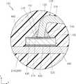
図1〜図6は、本発明の第1実施形態に基づく半導体装置を示している。本実施形態の半導体装置101は、第1リード100、第2リード200、半導体素子400、はんだ510,520および封止樹脂600を備えている。半導体装置101は、いわゆる2端子型の封止樹脂電子部品として構成されているが、これは本発明に係る半導体装置の一例であり3以上の端子を有する封止樹脂電子部品であってもよい。 1 to 6 show a semiconductor device according to the first embodiment of the present invention. The
図1は、半導体装置101を斜め上方向からみた斜視図である。図2は、図1のII−II線に沿うzx平面における断面図であり、図3および図4は、その要部拡大断面図である。図5は、半導体装置101の平面図であり、図6は、半導体装置101の側面図である。これらの図において、z方向は、本発明で言う第1方向に相当する。以下の説明においては、図1〜図3における図中上方を「上」、図中下方を「下」と便宜上称するが、z方向が重力方向と一致することを特定するものではない。また、x方向およびy方向は、平面方向を定義する方向として扱う。 FIG. 1 is a perspective view of the
半導体装置101の外形サイズの一例を挙げると、x方向寸法が5.0mm程度、y方向寸法が2.6mm程度、z方向寸法が2.0mm程度である。 As an example of the external size of the
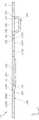
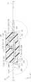
第1リード100は、半導体素子400に流れるべき電流の導通経路を構成するものであり、本実施形態においては、たとえばCuに代表される金属板からなる。本実施形態においては、第1リード100は、先端面110、起立部120、横行部130、段差部140、延伸部150、迂回部160および端子部170を有する。第1リード100の厚さは、たとえば0.2mm程度である。 The
図2および図3に示すように、先端面110は、z方向下方を向いており、後述する半導体装置101の製造方法から理解される通り、第1リード100の厚さ方向に起立する一端面であった面である。本実施形態においては、先端面110は、正方形とされており、そのサイズが0.2mm角程度とされている。 As shown in FIGS. 2 and 3, the
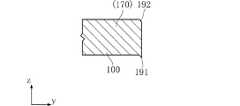
起立部120は、先端面110に繋がり、後述する半導体素子400の上面電極410から離間するように起立している。本実施形態においては、起立部120の断面は、一様な形状およびサイズとされており、先端面110と同じ0.2mm角程度の正方形である。また、起立部120の長さはたとえば0.6mm程度である。 The standing
図3によく表れているように、本実施形態においては、起立部120がz方向に対して若干傾いている。より具体的には、起立部120の上方部分が先端面110に対して図中右側に位置するように傾いている。また、先端面110は、起立部120に対して垂直であるため、左方部分が右方部分よりもz方向上方に位置するようにx方向に対して傾いている。先端面110においては、起立部120が傾く側(右側)とは反対側(左側)にバリ191が形成されている。また、起立部120が傾く側(右側)には、ダレ192が形成されている。なお、バリ191やダレ192は、後述するように半導体装置101の製造工程において不可避的に生じる可能性がある要素である。同様の製造工程を経た半導体装置101であっても、バリ191およびダレ192の両方が明瞭に形成される場合があれば、いずれか一方のみが形成される場合、もしくはいずれもが明瞭には形成されない場合がある。 As clearly shown in FIG. 3, in the present embodiment, the standing
横行部130は、起立部120に繋がり、かつz方向視において起立部120から離間するように延びる部位であり、本実施形態においては、図1、図2および図5に示すように、起立部120からx方向右方へと延びている。本実施形態の横行部130は、z方向厚さが0.2mm程度である。また、横行部130は、等幅部131および広幅部132を有している。等幅部131は、起立部120に繋がっており、y方向幅が起立部120と同じである。すなわち、等幅部131は、起立部120に対して連続的に繋がっており、y方向幅は、たとえば0.2mm程度である。広幅部132は、等幅部131に対して起立部120とは反対側(x方向右側)に繋がっており、等幅部131よりもy方向幅が広い。広幅部132のy方向幅は、たとえば0.9mm程度である。また、等幅部131および広幅部132のx方向寸法は、いずれもたとえば0.5mm程度である。なお、図2に示すように、本実施形態においては、横行部130は、x方向に対して若干傾いている。この傾き角度は、z方向に対する起立部120の傾き角度とほぼ同じである。 The traversing
段差部140は、一端が横行部130に対して起立部120とは反対側(図中右側)に繋がり、かつ他端が上記一端よりもz方向において半導体素子400側(z方向下方側)に位置する。すなわち、段差部140は、第1リード100に、z方向にシフトするクランク状の部分を生じさせている。さらに、本実施形態においては、段差部140は、z方向に対して傾いている。この傾き角度は、z方向に対する起立部120の傾き角度およびx方向に対する横行部130の傾き角度よりも若干大である。段差部140の厚さは0.2mm程度であり、y方向寸法は、1.4mm程度である。また、段差部140のz方向寸法は、0.6mm程度である。 One end of the stepped
延伸部150は、段差部140の図中下方側に繋がり、かつz方向視において段差部140から離間する方向(図中右方)に延びている。また、延伸部150は、後述する封止樹脂600からその一部が突出している。図1および図2に示すように、延伸部150は、x方向に対してほぼ平行である。延伸部のy方向寸法は1.4mm程度であり、z方向厚さは、0.2mm程度である。本実施形態においては、延伸部150に開口181が形成されている。開口181は、延伸部150の平面視におけるほぼ中央に配置されており、たとえばx方向寸法が0.3mm程度、y方向寸法が0.4mm程度の矩形状である。 The extending
迂回部160は、一端が延伸部150に対して段差部140とは反対側(図中右側)に繋がり、かつ他端が上記一端よりもz方向において段差部140よりも離間した位置(図中下方側位置)にある。本実施形態においては、迂回部160のy方向寸法は1.5mm程度であり、厚さが0.2mm程度である。また、本実施形態においては、図4および図5に示すように、延伸部150と迂回部160とが繋がる部分である折り曲げ部分に、溝182が形成されている。溝182は、上記折り曲げ部分において折り曲げ方向であるy方向に延びている。なお、本発明においては、折り曲げ加工によって形成された折り曲げ線が伸びる方向を便宜上「折り曲げ方向」と称する。また、溝182は、上記折り曲げ部分において折り曲げ内側に位置している。また、図5に示すように、溝182のy方向寸法は、上記折り曲げ部分のy方向寸法よりも小であり、溝182は上記折り曲げ部分のy方向両端には到達していない。後述するように、溝182は、たとえば断面三角形の溝であったものが折り曲げ加工の結果、断面形状が偏平となったものである。このため、溝182は、明瞭に開いた形状ではなく、ほとんど閉じた形状となる場合がありうる。溝182の深さは、たとえば0.07mm程度である。 The
端子部170は、迂回部160のz方向下端に繋がっており、この下端からx方向左方に延びている。端子部170は、半導体装置101がたとえば回路基板(図示略)などに面実装される際に実装端子として用いられる部位である。本実施形態においては、端子部170のy方向寸法は、たとえば1.5mm程度、厚さが0.2mm程度である。 The
第2リード200は、第1リード100とともに半導体素子400に流れるべき電流の導通経路を構成するものであり、本実施形態においては、たとえばCuに代表される金属板からなる。本実施形態においては、第2リード200は、ダイパッド部210、延伸部230、迂回部260および端子部270を有する。第2リード200の厚さは、たとえば0.2mm程度である。 The
ダイパッド部210は、半導体素子400が搭載される部位であり、第1リード100の先端面110に対して半導体素子400を挟んでz方向下方に位置している。図1および図5に示すように、ダイパッド部210は、z方向視において半導体素子400よりも大とされており、たとえばx方向寸法が2.2mm程度、y方向寸法が2.3mm程度の矩形状である。図2に示すように、本実施形態においては、ダイパッド部210は、第1リード100の延伸部150よりもz方向下方に位置している。 The
延伸部230は、ダイパッド部210に繋がり、z方向視において封止樹脂600の外部へとx方向左方に延びている。延伸部230は、y方向寸法がたとえば1.5mm程度とされており、ダイパッド部210よりもy方向の幅が狭い。また、図2に示すように、延伸部230は、ダイパッド部210に繋がる部分が封止樹脂600から突出する部分よりもz方向において第1リード100の先端面110に対して離間した位置、すなわちz方向下方側位置にある。より具体的には、延伸部230は、緩やかな2つの折り曲げ部分を有するクランク形状とされている。このクランク形状によるz方向のシフト距離は、たとえば0.15mm程度である。本実施形態においては、延伸部230に開口281が形成されている。開口281は、延伸部230の平面視におけるほぼ中央に配置されており、たとえばx方向寸法が0.4mm程度、y方向寸法が0.4mm程度の矩形状である。 The extending
迂回部260は、一端が延伸部230に対してダイパッド部210とは反対側(図中左方側)に繋がり、かつ他端が上記一端よりもz方向において延伸部230に対して離間した位置、すなわちz方向下方位置にある。本実施形態においては、迂回部260のy方向寸法は1.5mm程度である。また、本実施形態においては、図4および図5を参照して説明した溝182と同様に、延伸部230と迂回部260とが繋がる部分である折り曲げ部分に、溝282が形成されている。溝282は、上記折り曲げ部分において折り曲げ方向であるy方向に延びている。また、溝282は、上記折り曲げ部分において折り曲げ内側に位置している。また、図5に示すように、溝282のy方向寸法は、上記折り曲げ部分のy方向寸法よりも小であり、溝282は上記折り曲げ部分のy方向両端には到達していない。後述するように、溝282は、たとえば断面三角形の溝であったものが折り曲げ加工の結果、断面形状が偏平となったものである。このため、溝282は、明瞭に開いた形状ではなく、ほとんど閉じた形状となる場合がありうる。溝282の深さは、たとえば0.07mm程度である。 The
本実施形態においては、ダイパッド部210と延伸部230との間には、溝283が形成されている。溝283は、y方向に延びておりz方向上方に開口している。溝283の断面形状は、略三角形あるいは台形である。溝283は、後述するはんだ520の広がりを防止するとともに、第2リード200と封止樹脂600との接合強度を高める機能を果たす。 In the present embodiment, a
端子部270は、迂回部260のz方向下端に繋がっており、この下端からx方向右方方に延びている。端子部270は、半導体装置101がたとえば回路基板(図示略)などに面実装される際に実装端子として用いられる部位である。本実施形態においては、端子部270のy方向寸法は、たとえば1.5mm程度である。 The
半導体素子400は、半導体装置101がたとえば電気回路に組み込まれた際に、電気回路の一要素としての機能を果たすものであり、本実施形態においては、たとえばダイオードとして構成されている。半導体素子400は、上面電極410、下面電極420および絶縁層430を有している。半導体素子400のサイズの一例を挙げると、x方向寸法が0.90mm以上、1.70mm以下程度、y方向寸法が0.90mm以上、1.70mm以下程度、z方向高さが0.26mm程度である。 The
上面電極410は、本発明で言う電極に相当し、半導体素子400のz方向上面に形成されており、z方向上方を向いている。上面電極410は、たとえばAuなどの金属メッキ層からなる。本実施形態においては、図1および5に示すように、上面電極410は、平面視において半導体素子400の外形と相似形である矩形状であり、半導体素子400の平面視外縁よりも内方に退避した格好となっている。また、第1リード100の先端面110は、上面電極410よりも小である。平面視においては、先端面110と上面電極410との中心が互いにほぼ一致している。上面電極410のサイズの一例を挙げると、x方向寸法が0.60mm以上、1.40mm以下程度、y方向寸法が0.60mm以上、1.40mm以下程度である。 The
上面電極410と第1リード100の先端面110とは、はんだ510によって接合されている。はんだ510は、本発明で言う導電性接合材の一例に相当する。図1、図2および図5に示すように、z方向視においてはんだ510は上面電極410に内包されている。すなわち、はんだ510の外縁は、上面電極410の外縁よりも内側に退避している。また、はんだ510は、第1リード100の起立部120の一部に這い上がるように形成されている。はんだ510の這い上がり高さは、たとえば起立部120の半分程度である。 The
絶縁層430は、たとえばSiO2からなり、上面電極410を取り囲んでいる。また、絶縁層430の外縁は、半導体素子400のz方向視における外縁に到達している。本実施形態においては、絶縁層430は、矩形環状とされている。The insulating
下面電極420は、半導体素子400のz方向下面に形成されており、z方向下方を向いている。下面電極420は、はんだ520によって第2リード200のダイパッド部210に接合されている。 The
封止樹脂600は、半導体素子400、第1リード100の一部および第2リード200の一部を覆っており、これらを保護する機能を果たす。封止樹脂600は、たとえば黒色のエポキシ樹脂からなり、金型を用いて成形される。本実施形態においては、封止樹脂600のうち第1リード100および第2リード200が突出する位置よりもz方向上方に位置する部分は、偏平な錘台形とされている。また、封止樹脂600のz方向下方部分には、第1リード100の端子部170と第2リード200の端子部270とに挟まれた位置に、z方向下方に突出する突起が形成されている。 The sealing
また、図1および図5に示すように、半導体装置101は、4つの保持部12を有している。4つの保持部12は、それぞれが第1リード100および第2リード200と同様のたとえばCuなどの金属からなる。4つの保持部12は、z方向における位置が、第1リード100および第2リード200のうち封止樹脂600から突出する部位と同じである。4つの保持部12は、z方向視において封止樹脂600の四隅寄りに離間配置されている。それぞれの保持部12の1つのy方向端面は、封止樹脂600から露出している。保持部12は、半導体装置101の製造工程において、封止樹脂600を保持する役割を果たす。 Further, as shown in FIGS. 1 and 5, the
図2に示すように、本実施形態においては、z方向における第1リード100の横行部130と半導体素子400の上面電極410との距離H1は、z方向における横行部130と封止樹脂600の外面との距離H2よりも大である。たとえば、距離H1が0.43mm程度であるのに対し、距離H2は0.15mm程度である。また、横行部130の厚さtは、上述した通り0.2mm程度である。 As shown in FIG. 2, in the present embodiment, the distance H1 between the traversing
次に、半導体装置101の製造方法の一例について、図7〜図22を参照しつつ以下に説明する。 Next, an example of a method for manufacturing the
まず、図7および図8に示すように、リードフレーム10を用意する。リードフレーム10は、フレーム11と、このフレーム11に支持された複数の第1リード100および第2リード200とを含む。リードフレーム10は、たとえばCuなどの金属板であり、その厚さがたとえば0.2mm程度である。なお、図8から理解されるように、本図に示す第1リード100および第2リード200は、上述した第1リード100および第2リード200のように各所が折り曲げられた形状ではなく、いまだ平板状であり、正確には、第1リード100および第2リード200となるべき部位である。ただし、以降の説明においては、便宜上、それぞれを第1リード100および第2リード200と称する。また、第1リード100および第2リード200のうち折り曲げ加工が施される前の段階では、その形状が明確ではない部位については、かっこを付した符号によって表している。また、図中のx方向、y方向、z方向は厳密には妥当しない部分があるが、説明の便宜上、完成した半導体装置101を仮定した場合に妥当する方向に当てはめている。 First, as shown in FIGS. 7 and 8, a
図8に示すように、リードフレーム10においては、第1リード100と第2リード200とがx方向に並んで配置されている。第1リード100は、2つの連結部13によってフレーム11に連結されている。2つの連結部13は、第1リード100のうち迂回部160となるべき部位の近傍に繋がっており、y方向において互いに離間配置されている。連結部13のx方向寸法は0.2mm程度、y方向寸法は0.3mm程度である。 As shown in FIG. 8, in the
第2リード200は、端子部270となるべき部位の近傍がフレーム11に連結されている。 The
また、1組の第1リード100および第2リード200につき、4つの保持部12が形成されている。4つの保持部12は、フレーム11のうちy方向において第1リード100および第2リード200を挟む部位から突出している。 Further, four holding
本実施形態においては、リードフレーム10は、Cuの金属板を打ち抜き加工することによって形成されている。この打ち抜き加工においては、ダイとパンチが用いられる。このダイは、上記金属板に対してz方向下方に配置されるものであり、z方向視において上記金属板のうちリードフレーム10として残存すべき部位、すなわちフレーム11、複数の第1リード100および複数の第2リード200などの形状を有している。一方、上記パンチは、z方向視において上記金属板のうちリードフレーム10を形成するために除去されるべき部位の形状を有している。このパンチは、z方向上方から上記金属板を挟んで上記ダイと交差するようにz方向下方に押し下げられる。この結果、上記金属板に打ち抜き加工が施され、リードフレーム10が得られる。 In the present embodiment, the
このような打ち抜き加工を経ることにより、図9および図10に示すように、第1リード100が、バリ191およびダレ192を有し、第2リード200がバリ291およびダレ292を有する可能性がある。これらの図に示すように、上記パンチが向かってくるz方向上方側にダレ192,292が形成され、z方向下方側にバリ191,291が形成される。図7および図8に示す状態においては、すべてのバリ191,291とダレ192,292のz方向における向きは一律である。なお、上述した通り、バリ191,192やダレ192,292は、半導体装置101の製造工程において不可避的に生じる可能性がある要素である。同様の製造工程を経た場合であっても、バリ191,291およびダレ192,292の両方が明瞭に形成される場合があれば、いずれか一方のみが形成される場合、もしくはいずれもが明瞭には形成されない場合がある。 Through such punching, there is a possibility that the
また、第1リード100には、溝182が形成される。溝182は、延伸部150となるべき部位と迂回部160となるべき部位の間に形成され、図13に示すようにz方向上方の開口した断面三角形の溝である。ただし、溝182は、第1リード100のy方向両端には到達していない。一方、第2リード200には、溝282が形成される。溝282は、延伸部230となるべき部位と迂回部260となるべき部位との間に形成され、図12に示すようにz方向下方に開口した断面三角形の溝である。溝282も、第2リード200のy方向両端には到達していない。このように、溝182と溝282は、z方向において開口する向きが互いに逆である。このような溝182,282は、上述した打ち抜き加工と同時に、あるいは前後して形成してもよいし、後述する複数の折り曲げ加工の間に形成してもよい。 A
また、第2リード200には、溝283が形成される。溝283は、ダイパッド部210と延伸部230となるべき部位との間に形成され、図11に示すようにz方向上方に開口する断面略三角形または台形の溝である。溝283は、第2リード200のy方向両端に到達している。 A
次いで、図14および図15に示すように、第1リード100および第2リード200に対して折り曲げ加工を施す。第1リード100に対しては、先端面110が存在する端部から3箇所に対して折り曲げ加工を施す。これにより、起立部120、横行部130および段差部140が明瞭に現れる。また、第2リード200に対しては、ダイパッド部210よりも根元側の2箇所に対して折り曲げ加工を施す。これにより、クランク形状を有する延伸部230となるべき部位がより明瞭となる。この折り曲げ加工により、ダイパッド部210は、フレーム11に対してz方向下方に平行に移動した格好となる。また、第1リード100は、先端面110がz方向上方を向く姿勢となる。 Next, as shown in FIGS. 14 and 15, the
次いで、図16および図17に示すように、ダイパッド部210に半導体素子400を搭載する。半導体素子400の搭載は、たとえばダイパッド部210に上述したはんだ520となるべきはんだペースト520’を塗布し、この上に半導体素子400をマウントする。また、半導体素子400の上面電極410には、上述したはんだ510となるべきはんだペースト510’を塗布しておく。このはんだペースト510’は、上面電極410の中央付近にであって、上面電極410の外縁よりも内方に十分に退避した領域に塗布される。そして、第1リード100を、2つの連結部13を通るy方向に延びる軸を中心として図17における反時計回りにおよそ180°回転させる。これにより、2つの連結部13は、180°捻られる。また、先端面110がz方向上方を向く姿勢から、半導体素子400の上面電極410と対向する姿勢となる。 Next, as shown in FIGS. 16 and 17, the
なお、第1リード100を180°回転させると、第1リード100の先端面110、起立部120および横行部130は、図17において半導体素子400の近傍に想像線で示した位置に現れる。しかし、先端面110が上面電極410に当接することにより、第1リードのうち横行部130もしくはその近傍が若干撓むこととなる。これにより、起立部120がz方向に対して傾き、先端面110および横行部130がx方向に対して傾く。また、この際、先端面110のうち上面電極410に対して積極的に当接させられる部位は、図3に示した通りダレ192が形成された部位である。この後に、たとえばはんだペースト510’,520’を加熱によって硬化させる。これにより、はんだ510,520が形成され、第1リード100の先端面110と上面電極410との接合、および第2リード200のダイパッド部210と下面電極420との接合が完了する。 When the
次いで、図18に示すように、封止樹脂600を形成する。封止樹脂600は、たとえば、第1リード100および第2リード200の一部ずつを収容するキャビティーを有する金型を用いて成型する。このキャビティーには、4つの保持部12が収容される。このキャビティーにエポキシ樹脂などの樹脂材料を充填し、これを硬化させることにより、封止樹脂600が得られる。 Next, as shown in FIG. 18, a sealing
次いで、図18の2つの切断線CLに囲まれた領域を打ち抜き加工によって除去する。各切断線CLは、連結部13を含んでおり、また第1リード100の一部およびフレーム11の一部を含んでいる。本実施形態においては、切断線CLに囲まれた領域は、x方向寸法が2.3mm程度、y方向寸法が0.6mm程度である。この打ち抜きにより、2つの連結部13が除去され、第1リード100の迂回部160となるべき部位および端子部170となるべき部位がより明瞭となる。 Next, the region surrounded by the two cutting lines CL in FIG. 18 is removed by punching. Each cutting line CL includes the connecting
切断線CLに囲まれた領域の打ち抜きは、上述した打ち抜き加工と同様にダイとパンチとを用いて行う。この場合、上記パンチのz方向視形状が切断線CLに囲まれた領域の形状とされる。一方のダイは、このようなパンチが進入可能な開口を有する形状とされる。このダイがリードフレーム10のz方向下方に配置され、上記パンチがz方向上方からz方向下方へと押し下げられる。この結果、第1リード100のうち打ち抜き加工によって形成された端縁には、あらたなバリ191およびダレ192が形成されうる。すなわち、図20に示すように、第1リード100の端子部170となるべき部位のy方向端縁においては、z方向下方側にバリ191が存在し、z方向上方側にダレ192が存在する。一方、図19に示すように、たとえば第1リード100の端子部170となるべき部位のx方向端縁においては、z方向上方側にバリ191が存在し、z方向下方側にダレ192が存在する。これは、図8〜図10を参照して説明したバリ191およびダレ192を有しうる第1リード100が、図17を参照して説明した回転工程により、上下が反転した姿勢とされたからである。このように、第1リード100は、バリ191とダレ192とが存在しうる位置がその厚さ方向において互いに逆となる部位を有するものとなっている。 The area surrounded by the cutting line CL is punched using a die and a punch in the same manner as the above-described punching process. In this case, the shape of the punch viewed in the z direction is the shape of the region surrounded by the cutting line CL. One die is shaped to have an opening through which such a punch can enter. This die is disposed below the
次いで、図18に示すように、第2リード200とフレーム11とが連結された部位を除去する。この除去は、図18の切断線CLに囲まれた領域を除去するための打ち抜き加工と同時に行なってもよい。この結果、第1リード100および第2リード200がフレーム11から離間した構成となる。ただし、封止樹脂600は、フレーム11から延びる4つの保持部12を覆っている。このため、封止樹脂600は、フレーム11に保持された状態が保たれている。また、封止樹脂600を介して第1リード100および第2リード200も、フレーム11によって保持された状態が保たれている。そして、図21に示すように、第1リード100および第2リード200のうち封止樹脂600から突出した部位に対して2箇所ずつの折り曲げ加工を施す。これにより、迂回部160,260と端子部170,270とが形成される。なお、この際、溝182,282が、折り曲げの良好な起点となる。なお、図8および図13において、溝182はz方向上方に開口していたが、上述した回転工程を経た後は、溝282と同様にz方向下方に開口している。この後は、フレーム11から4つの保持部12を離間させるたとえば打ち抜き加工もしくは切断加工を経ることにより、図1に示した半導体装置101が得られる。 Next, as shown in FIG. 18, the portion where the
図22は、上述した製造工程を経て形成された第1リード100の単体を示す斜視図である。同図において、ハーフトーンが施された帯状部分は、破断面が形成されうる部分をしている。この破断面は、上述した製造工程での打ち抜き加工において、せん断過程に続いて第1リード100や第2リード200が引きちぎられるように切り離された部分の痕跡である。上記破断面は、第1リード100や第2リード200の各部位において、厚さ方向の一方側に現れる。打ち抜き加工の原理から、この破断面が存在する側に上述したバリ191が生じうる。本図における複数の微小な矢印は、バリ191が生じうる部分を示している。上述した通り、第1リード100は、反転させられる回転工程を挟んで、2度の打ち抜き加工が施される。このため、上記破断面およびバリ191が存在する部分が厚さ方向において互いに反対側となる2種類の部分が混在している。2度目の打ち抜きによって生じた端縁である、迂回部160および端子部170のy方向端縁は、上記破断面およびバリ191が生じうる側がそれ以外の部分とは反対となっている。 FIG. 22 is a perspective view showing a single
次に、半導体装置101およびその製造方法の作用について説明する。 Next, the operation of the
本実施形態によれば、図1、図2および図5に示すように、第1リード100は、先端面110のみが上面電極410と対向する姿勢で、はんだ510によって接合されている。このため、半導体装置101の製造工程において、上面電極410と第1リード100との間において、軟化したはんだが広い領域に及んでしまうことを防止することができる。これにより、第1リード100がずれてしまったり、はんだ510が上面電極410を超えて半導体素子400の側面に及んでしまうことを回避することができる。また、上面電極410から離間するように起立した起立部120を備えることにより、軟化したはんだが起立部120を伝って上昇することが期待できる。これにより、はんだ510を起立部120の近傍に留まらせることができる。したがって、半導体素子400の上面電極410と第1リード100とをより確実に接合することが可能である。 According to the present embodiment, as shown in FIGS. 1, 2, and 5, the
また、先端面110が、半導体素子400の上面電極410よりも小であることにより、はんだ510をより狭い領域に留まらせることができる。z方向視において、先端面110が半導体素子400の上面電極410の中心に重なっていることは、はんだ510が上面電極410を超えて周囲に及んでしまうことを回避するのに適している。z方向視において、はんだ510が、上面電極410に内包されていることにより、はんだ510と半導体素子400の側面との意図しない導通を排除することができる。z方向視において、半導体素子400の外形と上面電極410とが相似形であることにより、上面電極410を比較的大きくしつつ、上面電極410の外縁と半導体素子400の外縁との距離をばらつきなく小さくすることができる。先端面110が、正方形であることは、一般的な半導体素子400の上面電極410と相似形とするのに都合がよい。 Further, since the
第1リード100が、横行部130を有することにより、第1リード100を外部と導通させるための封止樹脂600からの突出部分を、半導体素子400からx方向に離間した位置に設けることができる。これは、半導体装置101の高さを低減するのに適している。また、図2における距離H1が、距離H2よりも大であることにより、はんだ510の起立部120に対する這い上がり高さをより高くすることができる。これは、はんだ510をより小さい領域に留まらせるのに適している。また、これに加えて、封止樹脂600の高さを低くすることに寄与し、半導体装置101の高さを低減するのに適している。 Since the
段差部140を備えることにより、半導体素子400のz方向上方を横断してきた横行部130から、z方向下方の半導体素子400に近い高さに第1リード100の一部を位置させることができる。そして、この段差部140に繋がる延伸部150が、x方向右方に延びて封止樹脂600から突出することにより、第1リード100を半導体素子400に近い高さに置くことができる。これは、封止樹脂600の高さを低減しつつ、第1リード100が封止樹脂600から突出する位置を偏らせないことができるという利点がある。 By providing the stepped
迂回部160および端子部170を有することにより、半導体装置101をいわゆる面実装タイプとして構成することができる。 By having the
延伸部150と迂回部160とが繋がる部分である折り曲げ部分に、溝182を設けることにより、第1リード100を封止樹脂600から確実に離間した位置において折り曲げることができる。溝182を封止樹脂600から離間させる一方、溝182と封止樹脂600との距離を適切に近づけることにより、半導体装置101の小型化を図ることができる。また、溝182が、y方向において上記折り曲げ部分よりも短く、第1リード100のy方向両端に到達していないことにより、上記折り曲げ部分が不当に弱い部分となってしまうことを防止することができる。 By providing the
横行部130が、等幅部131を有することにより、横行部130と起立部120との間の折り曲げ部分を正確に折り曲げ加工することができる。また、横行部130が、広幅部132を有することにより、横行部130の適切な高剛性化と低抵抗化とを図ることができる。 Since the
起立部120が、z方向に対して傾いており、先端面110のうち起立部120が傾く側とは反対側の部分(図3における図中左方側部分)に、バリ191が形成されている。これにより、バリ191を半導体素子400の上面電極410から離間させることができる。したがって、上面電極410がバリ191によって損傷を受けたり、バリ191のみが上面電極410と接し、先端面110が上面電極410から離間してしまうことを防止することができる。また、バリ191が形成される側とは反対側には、ダレ192が形成されやすい。この部分がバリ191よりも上面電極410に近い位置関係となることにより、先端面110を上面電極410により沿わせることができる。 The rising
半導体素子400に対して第1リード100の先端面110とは反対側から接合されたダイパッド部210を有することにより、半導体素子400をより確実に保持することができる。延伸部230を有することにより、第2リード200を外部と導通させるための封止樹脂600からの突出部分を、半導体素子400からx方向に離間した位置に設けることができる。これは、半導体装置101の高さを低減するのに適している。迂回部260および端子部270を有することにより、半導体装置101をいわゆる面実装タイプとして構成することができる。 By having the
延伸部230と迂回部260とが繋がる部分である折り曲げ部分に、溝282を設けることにより、第2リード200を封止樹脂600から確実に離間した位置において折り曲げることができる。溝282を封止樹脂600から離間させる一方、溝282と封止樹脂600との距離を適切に近づけることにより、半導体装置101の小型化を図ることができる。また、溝282が、y方向において上記折り曲げ部分よりも短く、第2リード200のy方向両端に到達していないことにより、上記折り曲げ部分が不当に弱い部分となってしまうことを防止することができる。 By providing the
半導体装置101の製造工程においては、上面電極410に対して先端面110が対向するように第1リード100を配置する工程と、上面電極410と先端面110とを接合する工程と、を備える。これにより、第1リード100のうちたとえばダイパッド部210に類似した比較的大きな面積の部位を上面電極410に対向させる必要がない。これは、半導体素子400のずれやはんだ510の広がりを抑えるのに適している。 The manufacturing process of the
第1リード100を配置する工程においては、先端面110がz方向上方を向く姿勢から先端面110が上面電極410と対向する姿勢へと第1リード100を回転させる。これにより、半導体素子400から離れた位置から第1リード100をたとえばスライドさせるなどの作業を経て第1リード100を配置する必要がない。したがって、第1リード100をより容易かつ確実に配置することができる。また、第1リード100を配置する工程においては、連結部13を捻ることにより第1リード100を回転させるとともに、第1リード100を配置する工程の後に、連結部13を除去する。これにより、上記第1リード100を連結部13を中心に安定して回転させることが可能であり、第1リード100の先端面110を上面電極410に対向する位置へと正確に導くことができる。連結部13を除去することにより、半導体装置101に不当に突出した部位が形成されてしまうことを回避することができる。 In the step of arranging the
図23は、本発明の他の実施形態を示している。なお、これらの図において、上記実施形態と同一または類似の要素には、上記実施形態と同一の符号を付している。同図に示された半導体装置102は、第3リード300を有する。 FIG. 23 shows another embodiment of the present invention. In these drawings, the same or similar elements as those in the above embodiment are denoted by the same reference numerals as those in the above embodiment. The
本実施形態においては、第1リード100は、先端面110、起立部120、横行部130、段差部140および延伸部150を有するものの、上述した迂回部160および端子部170は有していない。また、延伸部150が封止樹脂600から突出しない点が、上述した実施形態と異なる。第1リード100の先端面110、起立部120、横行部130、段差部140は、たとえば上述した実施形態と同様の構成である。 In the present embodiment, the
第3リード300は、第1リード100と導通しており、第1リード100と直列の関係で半導体素子400への導通経路を構成している。第3リード300は、延伸部350、迂回部360および端子部370を有する。第3リード300は、たとえば第1リード100および第2リード200と同様にCuなどの金属板からなり、その厚さがたとえば0.2mm程度である。延伸部350は、x方向に対して平行であり、第1リード100の延伸部150に対してたとえばはんだ530によって接合されている。迂回部360および端子部370は、上述した実施形態における迂回部160および端子部170と同様の構成である。また、第3リード300は、第1リード100と同様に、開口381および溝382を有する。 The
半導体装置102を形成する際には、第2リード200への半導体素子400の搭載を終えた後に、あらかじめ折り曲げ加工などによって形成した第1リード100を、半導体素子400の上面電極410と第3リード300の延伸部350とに跨るように配置する。そして、たとえばはんだペーストを硬化させることにより、接合が完了する。 When forming the
このような実施形態によっても、半導体素子400の上面電極410と第1リード100とをより確実に接合することが可能である。 Also according to such an embodiment, the
本発明に係る半導体装置およびその製造方法は、上述した実施形態に限定されるものではない。本発明に係る半導体装置およびその製造方法の具体的な構成は、種々に設計変更自在である。 The semiconductor device and the manufacturing method thereof according to the present invention are not limited to the above-described embodiments. The specific configuration of the semiconductor device and the manufacturing method thereof according to the present invention can be changed in various ways.
本発明で言う先端面と電極とは、確実に接触していることが好ましいが、導電性接合材による接合および導通が確実であれば、両者は離れていてもよい。先端面の形状は、正方形などの矩形状であることが、金属板から第1リードを形成する構成において便利であるが、先端面の形状はこれに限定されず、たとえば円形など電極の形状などに応じて適宜設定すればよい。第1リードは、複数の先端面および起立部を有する構成であってもよい。1つの電極に対して複数の先端面が対向する構成でもよい。あるいは、半導体素子が同じ側を向く複数の電極を有し、それぞれに先端面が個別に対向する構成であってもよい。さらに、1つの半導体素子に対して複数の第1リードが接合されている構成であってもよい。本発明で言う半導体素子は、ダイオードに限定されず、たとえばトランジスタやLEDなど、種々の構成が採用できる。 The tip surface and the electrode referred to in the present invention are preferably in contact with each other reliably, but they may be separated as long as the bonding and conduction by the conductive bonding material are reliable. The shape of the front end surface is a rectangular shape such as a square, which is convenient in the configuration in which the first lead is formed from a metal plate, but the shape of the front end surface is not limited to this, for example, the shape of an electrode such as a circle What is necessary is just to set suitably according to. The first lead may be configured to have a plurality of tip surfaces and standing parts. A configuration in which a plurality of tip surfaces face one electrode may be employed. Alternatively, the semiconductor element may have a plurality of electrodes facing the same side, and the tip surfaces may be individually opposed to each other. Further, a configuration in which a plurality of first leads are bonded to one semiconductor element may be employed. The semiconductor elements referred to in the present invention are not limited to diodes, and various configurations such as transistors and LEDs can be employed.
101,102 半導体装置
10 リードフレーム
11 フレーム
12 保持部
13 連結部
100 第1リード
110 先端面
120 起立部
130 横行部
131 等幅部
132 広幅部
140 段差部
150 延伸部
160 迂回部
170 端子部
181 開口
182 溝
191 バリ
192 ダレ
200 第2リード
210 ダイパッド部
230 延伸部
260 迂回部
270 端子部
281 開口
282,283 溝
291 バリ
292 ダレ
300 第3リード
350 延伸部
360 迂回部
370 端子部
381 開口
382 溝
400 半導体素子
410 上面電極
420 下面電極
430 絶縁層
510,520,530 はんだ(導電性接合材)
600 封止樹脂DESCRIPTION OF SYMBOLS 101,102
600 Sealing resin
Claims (30)
Translated fromJapanese上記電極に対向しかつ導通する先端面、およびこの先端面に繋がり上記電極から離間するように起立した起立部を有する第1リードと、
上記半導体素子の上記電極と上記第1リードの上記先端面とを接合する導電性接合材と、
上記半導体素子、上記第1リードの少なくとも一部、および上記導電性接合材を覆う封止樹脂と、
を備えることを特徴とする、半導体装置。A semiconductor element having an electrode facing the first direction;
A first lead having a tip surface facing and conductive with the electrode, and a standing portion connected to the tip surface and standing up to be separated from the electrode;
A conductive bonding material for bonding the electrode of the semiconductor element and the tip surface of the first lead;
A sealing resin covering the semiconductor element, at least a part of the first lead, and the conductive bonding material;
A semiconductor device comprising:
上記延伸部は、上記広幅部よりも幅が広い、請求項10ないし14のいずれかに記載の半導体装置。The traversing part is connected to the opposite side of the standing part with respect to the equal width part and the same width part as the width of the part connected to the standing part, and from the equal width part. Has a wide part with a wide width,
The semiconductor device according to claim 10, wherein the extended portion is wider than the wide portion.
上記先端面のうち上記起立部が傾く側とは反対側の部分に、バリが形成されている、請求項1ないし17のいずれかに記載の半導体装置。The upright portion is inclined with respect to the first direction,
18. The semiconductor device according to claim 1, wherein a burr is formed in a portion of the tip end surface opposite to the side on which the rising portion is inclined.
上記電極に対して上記先端面が対向するように上記第1リードを配置する工程と、
上記電極と上記先端面とを接合する工程と、
を備えることを特徴とする、半導体装置の製造方法。Preparing a semiconductor element having an electrode facing the first direction and a first lead having a tip surface;
Disposing the first lead so that the tip surface faces the electrode;
Bonding the electrode and the tip surface;
A method for manufacturing a semiconductor device, comprising:
上記第1リードを配置する工程の後に、上記連結部を除去する工程を備える、請求項28に記載の半導体装置の製造方法。In the step of arranging the first lead, the first lead is rotated by twisting a connecting portion connected to the first lead and extending in the axial direction of the rotation,
29. The method of manufacturing a semiconductor device according to claim 28, further comprising a step of removing the connecting portion after the step of arranging the first lead.
Priority Applications (2)
| Application Number | Priority Date | Filing Date | Title |
|---|---|---|---|
| JP2013065628AJP6239840B2 (en) | 2013-03-27 | 2013-03-27 | Semiconductor device and manufacturing method of semiconductor device |
| US14/226,280US9337129B2 (en) | 2013-03-27 | 2014-03-26 | Semiconductor device and method of manufacturing the same |
Applications Claiming Priority (1)
| Application Number | Priority Date | Filing Date | Title |
|---|---|---|---|
| JP2013065628AJP6239840B2 (en) | 2013-03-27 | 2013-03-27 | Semiconductor device and manufacturing method of semiconductor device |
Related Child Applications (1)
| Application Number | Title | Priority Date | Filing Date |
|---|---|---|---|
| JP2017212337ADivisionJP6417462B2 (en) | 2017-11-02 | 2017-11-02 | Semiconductor device |
Publications (2)
| Publication Number | Publication Date |
|---|---|
| JP2014192292Atrue JP2014192292A (en) | 2014-10-06 |
| JP6239840B2 JP6239840B2 (en) | 2017-11-29 |
Family
ID=51619998
Family Applications (1)
| Application Number | Title | Priority Date | Filing Date |
|---|---|---|---|
| JP2013065628AActiveJP6239840B2 (en) | 2013-03-27 | 2013-03-27 | Semiconductor device and manufacturing method of semiconductor device |
Country Status (2)
| Country | Link |
|---|---|
| US (1) | US9337129B2 (en) |
| JP (1) | JP6239840B2 (en) |
Cited By (5)
| Publication number | Priority date | Publication date | Assignee | Title |
|---|---|---|---|---|
| JP2018006453A (en)* | 2016-06-29 | 2018-01-11 | 日亜化学工業株式会社 | Light-emitting device, manufacturing method of the same, and manufacturing method of package |
| JP2018113359A (en)* | 2017-01-12 | 2018-07-19 | ローム株式会社 | Semiconductor device |
| JP2018125372A (en)* | 2017-01-31 | 2018-08-09 | ローム株式会社 | Semiconductor device and manufacturing method thereof |
| KR20210004066A (en)* | 2019-07-03 | 2021-01-13 | 제엠제코(주) | Semiconductor package |
| US11270969B2 (en) | 2019-06-04 | 2022-03-08 | Jmj Korea Co., Ltd. | Semiconductor package |
Families Citing this family (5)
| Publication number | Priority date | Publication date | Assignee | Title |
|---|---|---|---|---|
| DE102015102041A1 (en)* | 2015-02-12 | 2016-08-18 | Danfoss Silicon Power Gmbh | power module |
| US9818675B2 (en)* | 2015-03-31 | 2017-11-14 | Stmicroelectronics, Inc. | Semiconductor device including conductive clip with flexible leads and related methods |
| JP6508276B2 (en)* | 2016-09-28 | 2019-05-08 | 日亜化学工業株式会社 | Light emitting device and method of manufacturing the same |
| US10243107B2 (en)* | 2016-09-28 | 2019-03-26 | Nichia Corporation | Light emitting device and method for manufacturing thereof |
| US11069600B2 (en)* | 2019-05-24 | 2021-07-20 | Infineon Technologies Ag | Semiconductor package with space efficient lead and die pad design |
Citations (14)
| Publication number | Priority date | Publication date | Assignee | Title |
|---|---|---|---|---|
| JPS54104787A (en)* | 1978-02-03 | 1979-08-17 | Toshiba Corp | Lead frame for photo coupling element |
| JPH02126659A (en)* | 1988-09-09 | 1990-05-15 | Motorola Inc | Semiconductor device having curved bonding-lead and forming method thereof |
| JPH05315490A (en)* | 1992-05-07 | 1993-11-26 | Fuji Electric Co Ltd | Semiconductor element |
| JPH05326782A (en)* | 1992-05-21 | 1993-12-10 | Hitachi Ltd | Lead frame and semiconductor device using the same |
| JPH09129796A (en)* | 1995-10-27 | 1997-05-16 | Rohm Co Ltd | Semiconductor device |
| JP2001127100A (en)* | 1999-10-26 | 2001-05-11 | Sanken Electric Co Ltd | Semiconductor device and its manufacturing method |
| JP2002151554A (en)* | 2000-08-31 | 2002-05-24 | Nec Corp | Semiconductor device |
| JP2002280509A (en)* | 2001-03-15 | 2002-09-27 | Rohm Co Ltd | Semiconductor device and method for manufacturing the same |
| JP2003217557A (en)* | 2002-01-21 | 2003-07-31 | Tocad Energy Co Ltd | Lead plate bending structure |
| JP2006216736A (en)* | 2005-02-03 | 2006-08-17 | Matsushita Electric Ind Co Ltd | Semiconductor device and manufacturing method thereof |
| JP2007165714A (en)* | 2005-12-15 | 2007-06-28 | Renesas Technology Corp | Semiconductor device |
| JP2009038375A (en)* | 2007-08-02 | 2009-02-19 | Samsung Electronics Co Ltd | Semiconductor package device and manufacturing method thereof |
| JP2009049272A (en)* | 2007-08-22 | 2009-03-05 | Mitsubishi Electric Corp | Semiconductor device and manufacturing method thereof |
| JP2010287726A (en)* | 2009-06-11 | 2010-12-24 | Fuji Electric Systems Co Ltd | Semiconductor device |
Family Cites Families (20)
| Publication number | Priority date | Publication date | Assignee | Title |
|---|---|---|---|---|
| US3735208A (en)* | 1971-08-26 | 1973-05-22 | Rca Corp | Thermal fatigue lead-soldered semiconductor device |
| JPS6189643A (en)* | 1984-10-09 | 1986-05-07 | Toshiba Corp | Semiconductor device and its manufacturing method |
| US5583375A (en)* | 1990-06-11 | 1996-12-10 | Hitachi, Ltd. | Semiconductor device with lead structure within the planar area of the device |
| JP2747634B2 (en)* | 1992-10-09 | 1998-05-06 | ローム株式会社 | Surface mount type diode |
| TW270213B (en)* | 1993-12-08 | 1996-02-11 | Matsushita Electric Industrial Co Ltd | |
| JPH08264685A (en)* | 1995-03-27 | 1996-10-11 | Toshiba Corp | Resin-sealed semiconductor device and manufacturing method thereof |
| JPH09199645A (en)* | 1996-01-17 | 1997-07-31 | Mitsubishi Electric Corp | Semiconductor device and semiconductor module |
| JP4316019B2 (en)* | 1996-10-01 | 2009-08-19 | 株式会社東芝 | Semiconductor device and semiconductor device manufacturing method |
| KR100214561B1 (en)* | 1997-03-14 | 1999-08-02 | 구본준 | Rip Lead Package |
| JP2002203957A (en)* | 2000-12-28 | 2002-07-19 | Rohm Co Ltd | Transistor |
| JP3584887B2 (en)* | 2001-01-29 | 2004-11-04 | 株式会社村田製作所 | Manufacturing method of electronic components |
| TW540123B (en)* | 2002-06-14 | 2003-07-01 | Siliconware Precision Industries Co Ltd | Flip-chip semiconductor package with lead frame as chip carrier |
| JP2004214517A (en)* | 2003-01-08 | 2004-07-29 | Hitachi Ltd | Semiconductor device |
| JP2009200338A (en)* | 2008-02-22 | 2009-09-03 | Renesas Technology Corp | Method for manufacturing semiconductor device |
| JP5449959B2 (en)* | 2008-10-31 | 2014-03-19 | 三洋電機株式会社 | Cylindrical secondary battery |
| JPWO2011039795A1 (en)* | 2009-09-29 | 2013-02-21 | パナソニック株式会社 | Semiconductor device and manufacturing method thereof |
| JP2012182253A (en) | 2011-02-28 | 2012-09-20 | Sanken Electric Co Ltd | Semiconductor device |
| JP6121692B2 (en)* | 2012-11-05 | 2017-04-26 | ルネサスエレクトロニクス株式会社 | Semiconductor device and manufacturing method thereof |
| JP6230238B2 (en)* | 2013-02-06 | 2017-11-15 | 三菱電機株式会社 | Semiconductor device and manufacturing method thereof |
| JP6133093B2 (en)* | 2013-03-25 | 2017-05-24 | 本田技研工業株式会社 | Power converter |
- 2013
- 2013-03-27JPJP2013065628Apatent/JP6239840B2/enactiveActive
- 2014
- 2014-03-26USUS14/226,280patent/US9337129B2/enactiveActive
Patent Citations (14)
| Publication number | Priority date | Publication date | Assignee | Title |
|---|---|---|---|---|
| JPS54104787A (en)* | 1978-02-03 | 1979-08-17 | Toshiba Corp | Lead frame for photo coupling element |
| JPH02126659A (en)* | 1988-09-09 | 1990-05-15 | Motorola Inc | Semiconductor device having curved bonding-lead and forming method thereof |
| JPH05315490A (en)* | 1992-05-07 | 1993-11-26 | Fuji Electric Co Ltd | Semiconductor element |
| JPH05326782A (en)* | 1992-05-21 | 1993-12-10 | Hitachi Ltd | Lead frame and semiconductor device using the same |
| JPH09129796A (en)* | 1995-10-27 | 1997-05-16 | Rohm Co Ltd | Semiconductor device |
| JP2001127100A (en)* | 1999-10-26 | 2001-05-11 | Sanken Electric Co Ltd | Semiconductor device and its manufacturing method |
| JP2002151554A (en)* | 2000-08-31 | 2002-05-24 | Nec Corp | Semiconductor device |
| JP2002280509A (en)* | 2001-03-15 | 2002-09-27 | Rohm Co Ltd | Semiconductor device and method for manufacturing the same |
| JP2003217557A (en)* | 2002-01-21 | 2003-07-31 | Tocad Energy Co Ltd | Lead plate bending structure |
| JP2006216736A (en)* | 2005-02-03 | 2006-08-17 | Matsushita Electric Ind Co Ltd | Semiconductor device and manufacturing method thereof |
| JP2007165714A (en)* | 2005-12-15 | 2007-06-28 | Renesas Technology Corp | Semiconductor device |
| JP2009038375A (en)* | 2007-08-02 | 2009-02-19 | Samsung Electronics Co Ltd | Semiconductor package device and manufacturing method thereof |
| JP2009049272A (en)* | 2007-08-22 | 2009-03-05 | Mitsubishi Electric Corp | Semiconductor device and manufacturing method thereof |
| JP2010287726A (en)* | 2009-06-11 | 2010-12-24 | Fuji Electric Systems Co Ltd | Semiconductor device |
Cited By (7)
| Publication number | Priority date | Publication date | Assignee | Title |
|---|---|---|---|---|
| JP2018006453A (en)* | 2016-06-29 | 2018-01-11 | 日亜化学工業株式会社 | Light-emitting device, manufacturing method of the same, and manufacturing method of package |
| JP2018113359A (en)* | 2017-01-12 | 2018-07-19 | ローム株式会社 | Semiconductor device |
| JP2018125372A (en)* | 2017-01-31 | 2018-08-09 | ローム株式会社 | Semiconductor device and manufacturing method thereof |
| US11270969B2 (en) | 2019-06-04 | 2022-03-08 | Jmj Korea Co., Ltd. | Semiconductor package |
| US11676931B2 (en) | 2019-06-04 | 2023-06-13 | Jmj Korea Co., Ltd. | Semiconductor package |
| KR20210004066A (en)* | 2019-07-03 | 2021-01-13 | 제엠제코(주) | Semiconductor package |
| KR102327950B1 (en)* | 2019-07-03 | 2021-11-17 | 제엠제코(주) | Semiconductor package |
Also Published As
| Publication number | Publication date |
|---|---|
| JP6239840B2 (en) | 2017-11-29 |
| US9337129B2 (en) | 2016-05-10 |
| US20140291828A1 (en) | 2014-10-02 |
Similar Documents
| Publication | Publication Date | Title |
|---|---|---|
| JP6239840B2 (en) | Semiconductor device and manufacturing method of semiconductor device | |
| CN1208820C (en) | Semiconductor wafer, semiconductor device and manufacturing method thereof | |
| JP3935370B2 (en) | Bumped semiconductor element manufacturing method, semiconductor device and manufacturing method thereof, circuit board, and electronic device | |
| US11183444B2 (en) | Packaging of a semiconductor device with a plurality of leads | |
| JP3584930B2 (en) | Semiconductor device and manufacturing method thereof, circuit board, and electronic apparatus | |
| JP6244147B2 (en) | Manufacturing method of semiconductor device | |
| US8933518B2 (en) | Stacked power semiconductor device using dual lead frame | |
| JP6417462B2 (en) | Semiconductor device | |
| JP5125975B2 (en) | Resin case manufacturing method | |
| CN107564875A (en) | Semiconductor device | |
| JP2015072947A (en) | Semiconductor device and manufacturing method of the same | |
| JP6752639B2 (en) | Manufacturing method of semiconductor devices | |
| JP7175350B2 (en) | semiconductor equipment | |
| CN212365971U (en) | A chip diode with overflow-proof frame | |
| JP2020047758A (en) | Semiconductor device | |
| JP2012243943A (en) | Wire bonding structure, electronic apparatus, and manufacturing method of electronic apparatus | |
| JP2015041684A (en) | Manufacturing method of semiconductor device, semiconductor device, and lead frame | |
| JP2014225504A (en) | Resin multilayer substrate manufacturing method | |
| CN115116977B (en) | Semiconductor device and method for manufacturing the same | |
| JP2008270301A (en) | Semiconductor device | |
| JP2017199897A (en) | Semiconductor device | |
| CN102903645B (en) | Planar semiconductor element and manufacturing method thereof | |
| CN114175223A (en) | Power semiconductor module and method of forming a power semiconductor module | |
| JP2008112929A (en) | Circuit device, and manufacturing method of the same | |
| CN107331767B (en) | Semiconductor device with a plurality of transistors |
Legal Events
| Date | Code | Title | Description |
|---|---|---|---|
| A621 | Written request for application examination | Free format text:JAPANESE INTERMEDIATE CODE: A621 Effective date:20160210 | |
| A977 | Report on retrieval | Free format text:JAPANESE INTERMEDIATE CODE: A971007 Effective date:20161014 | |
| A131 | Notification of reasons for refusal | Free format text:JAPANESE INTERMEDIATE CODE: A131 Effective date:20161025 | |
| A521 | Request for written amendment filed | Free format text:JAPANESE INTERMEDIATE CODE: A523 Effective date:20161216 | |
| A131 | Notification of reasons for refusal | Free format text:JAPANESE INTERMEDIATE CODE: A131 Effective date:20170509 | |
| A521 | Request for written amendment filed | Free format text:JAPANESE INTERMEDIATE CODE: A523 Effective date:20170629 | |
| TRDD | Decision of grant or rejection written | ||
| A01 | Written decision to grant a patent or to grant a registration (utility model) | Free format text:JAPANESE INTERMEDIATE CODE: A01 Effective date:20171003 | |
| A61 | First payment of annual fees (during grant procedure) | Free format text:JAPANESE INTERMEDIATE CODE: A61 Effective date:20171102 | |
| R150 | Certificate of patent or registration of utility model | Ref document number:6239840 Country of ref document:JP Free format text:JAPANESE INTERMEDIATE CODE: R150 | |
| R250 | Receipt of annual fees | Free format text:JAPANESE INTERMEDIATE CODE: R250 | |
| R250 | Receipt of annual fees | Free format text:JAPANESE INTERMEDIATE CODE: R250 | |
| R250 | Receipt of annual fees | Free format text:JAPANESE INTERMEDIATE CODE: R250 | |
| R250 | Receipt of annual fees | Free format text:JAPANESE INTERMEDIATE CODE: R250 | |
| R250 | Receipt of annual fees | Free format text:JAPANESE INTERMEDIATE CODE: R250 |