JP2014187259A - Semiconductor device manufacturing method - Google Patents
Semiconductor device manufacturing methodDownload PDFInfo
- Publication number
- JP2014187259A JP2014187259AJP2013061842AJP2013061842AJP2014187259AJP 2014187259 AJP2014187259 AJP 2014187259AJP 2013061842 AJP2013061842 AJP 2013061842AJP 2013061842 AJP2013061842 AJP 2013061842AJP 2014187259 AJP2014187259 AJP 2014187259A
- Authority
- JP
- Japan
- Prior art keywords
- layer
- sige layer
- sige
- concentration
- forming
- Prior art date
- Legal status (The legal status is an assumption and is not a legal conclusion. Google has not performed a legal analysis and makes no representation as to the accuracy of the status listed.)
- Pending
Links
Images


Classifications
- H—ELECTRICITY
- H10—SEMICONDUCTOR DEVICES; ELECTRIC SOLID-STATE DEVICES NOT OTHERWISE PROVIDED FOR
- H10D—INORGANIC ELECTRIC SEMICONDUCTOR DEVICES
- H10D86/00—Integrated devices formed in or on insulating or conducting substrates, e.g. formed in silicon-on-insulator [SOI] substrates or on stainless steel or glass substrates
- H10D86/01—Manufacture or treatment
- H—ELECTRICITY
- H01—ELECTRIC ELEMENTS
- H01L—SEMICONDUCTOR DEVICES NOT COVERED BY CLASS H10
- H01L21/00—Processes or apparatus adapted for the manufacture or treatment of semiconductor or solid state devices or of parts thereof
- H01L21/02—Manufacture or treatment of semiconductor devices or of parts thereof
- H01L21/04—Manufacture or treatment of semiconductor devices or of parts thereof the devices having potential barriers, e.g. a PN junction, depletion layer or carrier concentration layer
- H01L21/18—Manufacture or treatment of semiconductor devices or of parts thereof the devices having potential barriers, e.g. a PN junction, depletion layer or carrier concentration layer the devices having semiconductor bodies comprising elements of Group IV of the Periodic Table or AIIIBV compounds with or without impurities, e.g. doping materials
- H01L21/30—Treatment of semiconductor bodies using processes or apparatus not provided for in groups H01L21/20 - H01L21/26
- H01L21/302—Treatment of semiconductor bodies using processes or apparatus not provided for in groups H01L21/20 - H01L21/26 to change their surface-physical characteristics or shape, e.g. etching, polishing, cutting
- H01L21/306—Chemical or electrical treatment, e.g. electrolytic etching
- H01L21/3065—Plasma etching; Reactive-ion etching
- H—ELECTRICITY
- H10—SEMICONDUCTOR DEVICES; ELECTRIC SOLID-STATE DEVICES NOT OTHERWISE PROVIDED FOR
- H10D—INORGANIC ELECTRIC SEMICONDUCTOR DEVICES
- H10D86/00—Integrated devices formed in or on insulating or conducting substrates, e.g. formed in silicon-on-insulator [SOI] substrates or on stainless steel or glass substrates
- H10D86/201—Integrated devices formed in or on insulating or conducting substrates, e.g. formed in silicon-on-insulator [SOI] substrates or on stainless steel or glass substrates the substrates comprising an insulating layer on a semiconductor body, e.g. SOI
- H—ELECTRICITY
- H10—SEMICONDUCTOR DEVICES; ELECTRIC SOLID-STATE DEVICES NOT OTHERWISE PROVIDED FOR
- H10D—INORGANIC ELECTRIC SEMICONDUCTOR DEVICES
- H10D84/00—Integrated devices formed in or on semiconductor substrates that comprise only semiconducting layers, e.g. on Si wafers or on GaAs-on-Si wafers
- H10D84/01—Manufacture or treatment
- H10D84/0123—Integrating together multiple components covered by H10D12/00 or H10D30/00, e.g. integrating multiple IGBTs
- H10D84/0126—Integrating together multiple components covered by H10D12/00 or H10D30/00, e.g. integrating multiple IGBTs the components including insulated gates, e.g. IGFETs
- H10D84/0165—Integrating together multiple components covered by H10D12/00 or H10D30/00, e.g. integrating multiple IGBTs the components including insulated gates, e.g. IGFETs the components including complementary IGFETs, e.g. CMOS devices
- H10D84/0167—Manufacturing their channels
- H—ELECTRICITY
- H10—SEMICONDUCTOR DEVICES; ELECTRIC SOLID-STATE DEVICES NOT OTHERWISE PROVIDED FOR
- H10D—INORGANIC ELECTRIC SEMICONDUCTOR DEVICES
- H10D84/00—Integrated devices formed in or on semiconductor substrates that comprise only semiconducting layers, e.g. on Si wafers or on GaAs-on-Si wafers
- H10D84/01—Manufacture or treatment
- H10D84/02—Manufacture or treatment characterised by using material-based technologies
- H10D84/03—Manufacture or treatment characterised by using material-based technologies using Group IV technology, e.g. silicon technology or silicon-carbide [SiC] technology
- H10D84/038—Manufacture or treatment characterised by using material-based technologies using Group IV technology, e.g. silicon technology or silicon-carbide [SiC] technology using silicon technology, e.g. SiGe
- Y—GENERAL TAGGING OF NEW TECHNOLOGICAL DEVELOPMENTS; GENERAL TAGGING OF CROSS-SECTIONAL TECHNOLOGIES SPANNING OVER SEVERAL SECTIONS OF THE IPC; TECHNICAL SUBJECTS COVERED BY FORMER USPC CROSS-REFERENCE ART COLLECTIONS [XRACs] AND DIGESTS
- Y10—TECHNICAL SUBJECTS COVERED BY FORMER USPC
- Y10S—TECHNICAL SUBJECTS COVERED BY FORMER USPC CROSS-REFERENCE ART COLLECTIONS [XRACs] AND DIGESTS
- Y10S438/00—Semiconductor device manufacturing: process
- Y10S438/933—Germanium or silicon or Ge-Si on III-V
Landscapes
- Engineering & Computer Science (AREA)
- Physics & Mathematics (AREA)
- General Physics & Mathematics (AREA)
- Condensed Matter Physics & Semiconductors (AREA)
- Manufacturing & Machinery (AREA)
- Computer Hardware Design (AREA)
- Microelectronics & Electronic Packaging (AREA)
- Power Engineering (AREA)
- Plasma & Fusion (AREA)
- Metal-Oxide And Bipolar Metal-Oxide Semiconductor Integrated Circuits (AREA)
- Thin Film Transistor (AREA)
- General Chemical & Material Sciences (AREA)
- Chemical Kinetics & Catalysis (AREA)
- Chemical & Material Sciences (AREA)
Abstract
Translated fromJapaneseDescription
Translated fromJapanese実施形態は、半導体装置の製造方法に関する。 Embodiments described herein relate generally to a method for manufacturing a semiconductor device.
CMOS回路では、高速動作のため、pチャネルFETは、ホールの移動度が高いGeチャネル又はSiGeチャネルを使用することが望ましい。また、nMOSは、電子の移動度が高いSiチャネルを使用することが望ましい。 In a CMOS circuit, it is desirable to use a Ge channel or a SiGe channel with high hole mobility for the p-channel FET for high-speed operation. The nMOS preferably uses a Si channel with high electron mobility.
一方、CMOS回路では、短チャネル効果を防止するため、絶縁層上にチャネルを形成することが望ましい。このため、pチャネルFETでは、GOI(Germanium on insulator)基板又はSGOI(Silicon Germanium on insulator)基板が用いられ、nチャネルFETでは、SOI(Silicon On insulator)基板が用いられる。 On the other hand, in a CMOS circuit, it is desirable to form a channel on an insulating layer in order to prevent a short channel effect. For this reason, a p-channel FET uses a GOI (Germanium on insulator) substrate or a SGOI (Silicon Germanium on insulator) substrate, and an n-channel FET uses a SOI (Silicon On Insulator) substrate.
しかし、1つの基板上に、pチャネルFETに適したGeチャネル又はSiGeチャネルと、nチャネルFETに適したSiチャネルとを、低コストで形成することは難しい。 However, it is difficult to form a Ge channel or SiGe channel suitable for a p-channel FET and a Si channel suitable for an n-channel FET on a single substrate at low cost.
実施形態は、1つの基板上に、Ge/SiGeチャネルを選択的に形成可能な製造方法を提案する。 The embodiment proposes a manufacturing method capable of selectively forming a Ge / SiGe channel on one substrate.
実施形態によれば、半導体装置の製造方法は、半導体基板上に、第1のGe濃度を有する第1のSiGe層を形成する工程と、前記第1のSiGe層上に、前記第1のGe濃度のピークよりも低い第2のGe濃度を有する第2のSiGe層を形成する工程と、前記第2のSiGe層上にマスク層を形成する工程と、前記マスク層をマスクにした異方性エッチングにより、前記第1及び第2のSiGe層をエッチングし、トレンチを形成する工程と、前記トレンチ内に露出した前記第1のSiGe層を選択的に除去し、前記第2のSiGe層下に空洞を形成する工程と、前記トレンチ及び前記空洞内に露出した前記第2のSiGe層の側面及び下面を酸化することにより、前記第2のSiGe層の前記第1のGe濃度を上昇させる工程とを備える。 According to the embodiment, a method of manufacturing a semiconductor device includes a step of forming a first SiGe layer having a first Ge concentration on a semiconductor substrate, and the first GeGe on the first SiGe layer. Forming a second SiGe layer having a second Ge concentration lower than a concentration peak; forming a mask layer on the second SiGe layer; and anisotropy using the mask layer as a mask Etching the first and second SiGe layers by etching to form a trench, and selectively removing the first SiGe layer exposed in the trench, under the second SiGe layer Forming a cavity; and increasing the first Ge concentration of the second SiGe layer by oxidizing the trench and the side and bottom surfaces of the second SiGe layer exposed in the cavity; With .
以下、図面を参照しながら実施形態を説明する。 Hereinafter, embodiments will be described with reference to the drawings.
[概要]
以下の実施例は、1つの基板上に、Ge/SiGeチャネル(アクティブエリア)を選択的に形成可能な製造方法について提案する。[Overview]
The following embodiments propose a manufacturing method capable of selectively forming a Ge / SiGe channel (active area) on one substrate.
例えば、まず、半導体基板上に、第1のGe濃度を有する第1のSiGe層を形成し、第1のSiGe層上に、第1のGe濃度のピークよりも低い第2のGe濃度を有する第2のSiGe層を形成する。また、マスク層をマスクにした異方性エッチング(例えば、RIE)により、第1及び第2のSiGe層をエッチングし、トレンチを形成する。 For example, first, a first SiGe layer having a first Ge concentration is formed on a semiconductor substrate, and a second Ge concentration lower than the peak of the first Ge concentration is formed on the first SiGe layer. A second SiGe layer is formed. Further, the first and second SiGe layers are etched by anisotropic etching (for example, RIE) using the mask layer as a mask to form a trench.
この後、第1のSiGe層と第2のSiGe層とのエッチングレートの差を利用することにより、トレンチ内に露出した第1のSiGe層のみを選択的に除去し、第2のSiGe層下に空洞を形成する。 Thereafter, by utilizing the difference in etching rate between the first SiGe layer and the second SiGe layer, only the first SiGe layer exposed in the trench is selectively removed, and the second SiGe layer is removed. A cavity is formed in.
そして、トレンチ及び空洞内に露出した第2のSiGe層の側面及び下面を酸化することにより、第2のSiGe層の第1のGe濃度を上昇させれば(Geの濃縮酸化)、1つの基板上に、Ge/SiGeチャネルを選択的に形成することができる。 Then, if the first Ge concentration of the second SiGe layer is increased by oxidizing the side surface and the lower surface of the second SiGe layer exposed in the trench and the cavity (Ge enriched oxidation), one substrate On top, Ge / SiGe channels can be selectively formed.
尚、Geの濃縮酸化において、第2のSiGe層内のSiを全て消費させれば、第2のSiGe層は、Ge層となる。即ち、Geの濃縮酸化の程度により、1つの基板上に形成されるチャネルを、SiGeチャネルにするか、又は、Geチャネルにするか、を制御することができる。 In addition, if all the Si in the second SiGe layer is consumed in the Ge concentration oxidation, the second SiGe layer becomes a Ge layer. That is, it is possible to control whether a channel formed on one substrate is a SiGe channel or a Ge channel depending on the degree of Ge enrichment oxidation.
また、第1のSiGe層を選択的に除去する前において、第1のGe濃度は、第1のSiGe層内で、一定でもよいし、変化してもよい。同様に、第2のGe濃度は、第2のSiGe層内で、一定でもよいし、変化してもよい。即ち、第2のSiGe層の第2のGe濃度が、第1のSiGe層の第1のGe濃度のピークよりも低ければよい。 Further, before the first SiGe layer is selectively removed, the first Ge concentration may be constant or may vary within the first SiGe layer. Similarly, the second Ge concentration may be constant or may vary within the second SiGe layer. That is, it is sufficient that the second Ge concentration of the second SiGe layer is lower than the peak of the first Ge concentration of the first SiGe layer.
例えば、半導体基板がSiの場合、第1のSiGe層の結晶状態を良くするために、第1のSiGe層と半導体基板との界面領域において、第1のSiGe層の第1のGe濃度は、できるだけ低い(Siに近い)のが望ましい。 For example, when the semiconductor substrate is Si, in order to improve the crystal state of the first SiGe layer, in the interface region between the first SiGe layer and the semiconductor substrate, the first Ge concentration of the first SiGe layer is It is desirable to be as low as possible (close to Si).
この場合、第1のSiGe層と半導体基板との界面領域において、第1のSiGe層の第1のGe濃度は、第2のSiGe層の第2のGe濃度よりも低くても構わない。但し、SiGeのエッチングレートは、Ge濃度が高くなるほど速くなるため、最低限の条件として、第1のSiGe層の第1のGe濃度のピークは、第2のSiGe層の第2のGe濃度よりも高いことが必要である。これは、第2のSiGe層内のどの部分においても満たされている必要がある。 In this case, in the interface region between the first SiGe layer and the semiconductor substrate, the first Ge concentration of the first SiGe layer may be lower than the second Ge concentration of the second SiGe layer. However, since the etching rate of SiGe increases as the Ge concentration increases, as a minimum condition, the peak of the first Ge concentration of the first SiGe layer is lower than the second Ge concentration of the second SiGe layer. It is necessary to be high. This needs to be satisfied everywhere in the second SiGe layer.
また、例えば、製造上の理由から、第1のSiGe層を選択的に除去する前において、第1及び第2のGe濃度は、それぞれ、第1及び第2のSiGe層内で、連続的又は不連続的に変化してもよいし、その中に一定の部分を有していてもよい。 Also, for example, for manufacturing reasons, before selectively removing the first SiGe layer, the first and second Ge concentrations may be continuous or first or second in the first and second SiGe layers, respectively. It may change discontinuously or may have a certain part in it.
尚、第2のSiGe層の側面及び下面を酸化した後に、トレンチ及び空洞は、そのままにしておいてもよいし、それらを絶縁層(例えば、SiO2)で満たしてもよい。トレンチ及び空洞は、FETの寄生容量を抑えるために望ましいが、FETの物理的強度を弱めるデメリットを有する。In addition, after oxidizing the side surface and the lower surface of the second SiGe layer, the trench and the cavity may be left as they are, or they may be filled with an insulating layer (for example, SiO2 ). Although trenches and cavities are desirable to reduce the parasitic capacitance of the FET, they have the disadvantage of reducing the physical strength of the FET.
そこで、FETの物理的強度が問題となるような場合には、トレンチ及び空洞は、絶縁層で満たしておくのが望ましい。 Therefore, when the physical strength of the FET becomes a problem, the trench and the cavity are preferably filled with an insulating layer.
以上のような製造方法によれば、例えば、1つの基板上に、pチャネルFETに適したGeチャネル又はSiGeチャネルと、nチャネルFETに適したSiチャネルとを、低コストで形成することができる。 According to the above manufacturing method, for example, a Ge channel or SiGe channel suitable for a p-channel FET and a Si channel suitable for an n-channel FET can be formed on one substrate at a low cost. .
例えば、半導体基板上に絶縁層を形成し、絶縁層上にSi層を形成し、第2のSiGe層上にpチャネルFETを形成し、かつ、Si層上にnチャネルFETを形成すれば、簡易なプロセスにより、CMOS回路を形成することができる。 For example, if an insulating layer is formed on a semiconductor substrate, an Si layer is formed on the insulating layer, a p-channel FET is formed on the second SiGe layer, and an n-channel FET is formed on the Si layer, A CMOS circuit can be formed by a simple process.
[実施例]
図1乃至図21は、半導体装置の製造方法を示している。[Example]
1 to 21 show a method for manufacturing a semiconductor device.
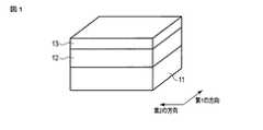
まず、図1に示すように、例えば、エピタキシャル成長法により、半導体基板(例えば、Si基板)11上に、例えば、200nmの厚さを持つ第1のSiGe層12を形成する。第1のSiGe層12内のSiとGeの組成比は、例えば、Si:Ge=60:40である。ここでは、これをGe濃度が40%であると称する。 First, as shown in FIG. 1, a
また、例えば、エピタキシャル成長法により、第1のSiGe層12上に、例えば、45nmの厚さを持つ第2のSiGe層13を形成する。第2のSiGe層13内のSiとGeの組成比は、例えば、Si:Ge=80:20である。ここでは、これをGe濃度が20%であると称する。 Further, for example, the
本例では、第1及び第2のSiGe層12,13内のSiとGeの組成比は、一定、即ち、第1及び第2のSiGe層12,13内のGe濃度は、一定であるとする。 In this example, the composition ratio of Si and Ge in the first and second SiGe layers 12 and 13 is constant, that is, the Ge concentration in the first and second SiGe layers 12 and 13 is constant. To do.
次に、図2に示すように、第2のSiGe層13上にマスク層MKを形成する。マスク層MKは、レジスト層であってもよいし、SiO2やSiNなどのハードマスク層であってもよい。この後、このマスク層MKをマスクにした異方性エッチング、例えば、RIEにより、第1及び第2のSiGe層12,13をエッチングすると、図3に示す構造が得られる。この後、マスク層MKは、除去される。Next, as shown in FIG. 2, a mask layer MK is formed on the
次に、図4に示すように、例えば、LPCVD法により、半導体基板11上に、第1及び第2のSiGe層12,13を完全に満たす、例えば、300nmの厚さを持つ絶縁層(例えば、SiO2)14を形成する。また、図5に示すように、CMP法により、絶縁層14の上面を研磨し、第2のSiGe層13の上面を、絶縁層14から露出させる。Next, as shown in FIG. 4, for example, an insulating layer (for example, a thickness of 300 nm) that completely fills the first and second SiGe layers 12 and 13 on the
これにより、例えば、支持体としての絶縁層14により取り囲まれた第1及び第2のSiGe層12,13が形成される。 Thereby, for example, the first and second SiGe layers 12 and 13 surrounded by the insulating
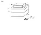
次に、例えば、LPCVD法により、図6に示すように、第2のSiGe層13上に、ハードマスク層(SiO2やSiNなどの絶縁層)15を形成する。ハードマスク層15は、例えば、第2の方向に一定幅を持ち、第1の方向に延びるライン形状を有する。第2のSiGe層13とハードマスク層15とのオーバーラップ部分が、アクティブエリアとなる。Next, a hard mask layer (insulating layer such as SiO2 or SiN) 15 is formed on the
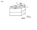
次に、図7乃至図9に示すように、異方性エッチング(例えば、RIE)により、第1及び第2のSiGe層12,13をエッチングする。その結果、ハードマスク層15により覆われた第1及び第2のSiGe層12,13と絶縁層14とにより囲まれる部分に、トレンチTR1,TR2が形成される。 Next, as shown in FIGS. 7 to 9, the first and second SiGe layers 12 and 13 are etched by anisotropic etching (for example, RIE). As a result, trenches TR1 and TR2 are formed in portions surrounded by the first and second SiGe layers 12 and 13 and the insulating
尚、2つのトレンチTR1,TR2間の第2のSiGe層13は、アクティブエリアAAとなる。 Note that the
この後、トレンチTR1,TR2に露出した第1のSiGe層12を選択的に除去すると、図10乃至図12に示す構造が得られる。即ち、図10乃至図12から明らかなように、第2のSiGe層13の直下に、第1及び第2のトレンチTR1,TR2を接続する空洞CVが形成される。 Thereafter, when the
ここで、空洞CVの形成に関して、第1のSiGe層12のGe濃度(Geの組成比)が第2のSiGe層13のGe濃度(Geの組成比)よりも大きいため、第2のSiGe層13のエッチングを抑制しつつ、第1のSiGe層12のみを選択的にエッチングすることができる。 Here, since the Ge concentration (Ge composition ratio) of the
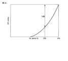
図22は、SiGe層のエッチングレートの変化を示している。 FIG. 22 shows a change in the etching rate of the SiGe layer.
同図において、横軸は、Ge濃度(atomic%)を示し、縦軸は、エッチングレートE/R(nm/min)を示す。 In the figure, the horizontal axis indicates the Ge concentration (atomic%), and the vertical axis indicates the etching rate E / R (nm / min).
エッチング条件としては、例えば、エッチングガス:H2及びHCl、エッチング温度:600℃〜700℃、エッチング時間:60分である。Etching conditions are, for example, etching gas: H2 and HCl, etching temperature: 600 ° C. to 700 ° C., and etching time: 60 minutes.
同図から明らかなように、SiGe層内のGe濃度が高くなると、エッチングレートも高くなる。これは、SiGe層内のGe濃度が高いと、SiGe層とエッチングガスとの反応が活発に起こることを示している。例えば、本例のように、第1のSiGe層12のGe濃度が40%であり、第2のSiGe層13のGe濃度が20%であるとき、エッチングレートの差は、約10倍となる。 As is clear from the figure, the etching rate increases as the Ge concentration in the SiGe layer increases. This indicates that when the Ge concentration in the SiGe layer is high, the reaction between the SiGe layer and the etching gas occurs actively. For example, as in this example, when the Ge concentration of the
このように、第1及び第2のSiGe層12,13内のGe濃度の差を用いることにより、第1のSiGe層12のみを選択的にエッチングすることができる。 Thus, by using the difference in Ge concentration in the first and second SiGe layers 12 and 13, only the
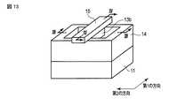
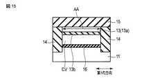
次に、図13乃至図15に示すように、トレンチTR1,TR2及び空洞CV内に露出した第2のSiGe層13(13a)の側面及び下面を酸化することにより、第2のSiGe層13の側面上及び下面上に、酸化層13bを形成する。 Next, as shown in FIGS. 13 to 15, the side surfaces and the lower surface of the second SiGe layer 13 (13a) exposed in the trenches TR1 and TR2 and the cavity CV are oxidized to thereby form the
その結果、第2のSiGe層13(13a)のGe濃度を上昇させることができる(Geの濃縮酸化)。 As a result, the Ge concentration of the second SiGe layer 13 (13a) can be increased (concentrated oxidation of Ge).
例えば、Ge濃度20%、厚さ40nmの第2のSiGe層13(13a)を、950℃のO2雰囲気中で、30nm(厚さ40nmの75%)酸化するとき、第2のSiGe層13(13a)のGe濃度は、80%乃〜90%に濃縮される。For example, when the second SiGe layer 13 (13a) having a Ge concentration of 20% and a thickness of 40 nm is oxidized in an O2 atmosphere at 950 ° C. by 30 nm (75% of the thickness of 40 nm), the
このような原理により、第2のSiGe層13(13a)内のSiを全て消費させ、第2のSiGe層13(13a)をGe層にすることも可能である。 Based on such a principle, it is also possible to consume all of the Si in the second SiGe layer 13 (13a) and make the second SiGe layer 13 (13a) a Ge layer.
尚、酸化層16は、上述のGeの濃縮酸化時に付随的に形成された半導体基板(例えば、Si基板)11の酸化層である。 The
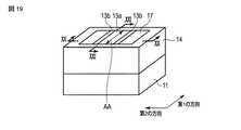
次に、図16乃至図18に示すように、例えば、LPCVD法により、トレンチTR1,TR2及び空洞CV内に、絶縁層(例えば、SiO2)17を満たす。このプロセスは、既に述べたように、省略してもよい。Next, as shown in FIGS. 16 to 18, the insulating layer (for example, SiO2 ) 17 is filled in the trenches TR 1 and
最後に、例えば、ウェットエッチングにより、ハードマスク層15を除去すると、図19乃至図21に示すように、絶縁層17上に、アクティブエリア(Geチャネル又はSiGeチャネル)AAを有する半導体装置が完成する。 Finally, when the
そして、例えば、CMOSプロセスにより、このアクティブエリアAA上にpチャネルFETが形成される。 Then, for example, a p-channel FET is formed on the active area AA by a CMOS process.
[変形例]
上述の実施例において、第1及び第2のSiGe層12,13内のGe濃度は、第1及び第2のSiGe層12,13内で変化させてもよい。[Modification]
In the above-described embodiment, the Ge concentration in the first and second SiGe layers 12 and 13 may be changed in the first and second SiGe layers 12 and 13.
例えば、図23に示すように、第1及び第2のSiGe層12,13内のGe濃度に濃度勾配を設けることも可能である。 For example, as shown in FIG. 23, it is possible to provide a concentration gradient in the Ge concentration in the first and second SiGe layers 12 and 13.
第1のSiGe層12内のGe濃度のピークPから半導体基板(Si基板)11側のエリアCでは、半導体基板(Si基板)11と第1のSiGe層12との結晶構造の不連続(結晶状態の悪化)に起因するラフネスを防止するため、半導体基板11と第1のSiGe層12との界面領域においては、第1のSiGe層12のGe濃度は、できるだけ低いのが望ましい。 In the area C on the semiconductor substrate (Si substrate) 11 side from the Ge concentration peak P in the
この場合、半導体基板11と第1のSiGe層12との界面領域において、第1のSiGe層12のGe濃度は、第2のSiGe層13のGe濃度よりも低くても構わない。 In this case, the Ge concentration of the
同様の理由から、第1のSiGe層12内のGe濃度のピークPから第2のSiGe層13側のエリアDでは、第1及び第2のSiGe層12,13との結晶構造の不連続(結晶状態の悪化)に起因するラフネスを防止するため、第1及び第2のSiGe層12,13との界面領域においては、第1のSiGe層12のGe濃度は、第2のSiGe層13内のGe濃度に緩やかに近づくのが望ましい。 For the same reason, in the area D on the
[適用例]
上述の製造方法により形成されたSGOI基板又はGOI基板を用いて、CMOS回路を形成する適用例を説明する。[Application example]
An application example in which a CMOS circuit is formed using the SGOI substrate or the GOI substrate formed by the above-described manufacturing method will be described.
図24は、CMOS回路を示している。 FIG. 24 shows a CMOS circuit.
pチャネルFETは、例えば、半導体装置11上の絶縁層17上のSiGe層(Ge層)13a上に形成される。ここで、半導体装置11、SiGe層(Ge層)13a、及び、絶縁層17は、それぞれ、例えば、図19乃至図21に示す、半導体基板11、SiGe層(Ge層)13a、及び、絶縁層17に相当する。 The p-channel FET is formed on, for example, a SiGe layer (Ge layer) 13 a on the insulating
また、nチャネルFETは、半導体基板11上の絶縁層20上のSi層21上に形成される。Si層21は、SiGe層(Ge層)13aを形成した後に形成してもよいし、また、SiGe層(Ge層)13aを形成する前に形成してもよい。 The n-channel FET is formed on the
また、上述の製造方法を用いて、例えば、SOI基板内に、部分的に、SiGe層(Ge層)13aを形成した後、SOI基板内のSi層上に、nチャネルFETを形成し、SiGe層(Ge層)13a上に、pチャネルFETを形成することも可能である。 Further, for example, after the SiGe layer (Ge layer) 13a is partially formed in the SOI substrate by using the manufacturing method described above, an n-channel FET is formed on the Si layer in the SOI substrate, and SiGe A p-channel FET can be formed on the layer (Ge layer) 13a.
[むすび]
以上、実施形態によれば、1つの基板上に、Geチャネル/SiGeチャネルを選択的に形成することができる。[Musubi]
As described above, according to the embodiment, a Ge channel / SiGe channel can be selectively formed on one substrate.
本発明のいくつかの実施形態を説明したが、これらの実施形態は、例として提示したものであり、発明の範囲を限定することは意図していない。これら新規な実施形態は、その他の様々な形態で実施されることが可能であり、発明の要旨を逸脱しない範囲で、種々の省略、置き換え、変更を行うことができる。これら実施形態やその変形は、発明の範囲や要旨に含まれるとともに、特許請求の範囲に記載された発明とその均等の範囲に含まれる。 Although several embodiments of the present invention have been described, these embodiments are presented by way of example and are not intended to limit the scope of the invention. These novel embodiments can be implemented in various other forms, and various omissions, replacements, and changes can be made without departing from the scope of the invention. These embodiments and modifications thereof are included in the scope and gist of the invention, and are included in the invention described in the claims and the equivalents thereof.
11:Si基板、12:第1のSiGe層、13:第2のSiGe層、13a:Ge部分、13b:第1の酸化膜、14:埋め込み絶縁層、15:ハードマスク層、16:第2の酸化膜、17:絶縁層、18:nチャネル材料、19:ゲート酸化膜、20:ゲート電極、21:サイドウォール、22a、22b:ソース/ドレイン領域、AA:アクティブエリア 11: Si substrate, 12: first SiGe layer, 13: second SiGe layer, 13a: Ge portion, 13b: first oxide film, 14: buried insulating layer, 15: hard mask layer, 16: second Oxide film, 17: insulating layer, 18: n-channel material, 19: gate oxide film, 20: gate electrode, 21: sidewall, 22a, 22b: source / drain region, AA: active area
Claims (5)
Translated fromJapanese前記第1のSiGe層上に、前記第1のGe濃度のピークよりも低い第2のGe濃度を有する第2のSiGe層を形成する工程と、
前記第2のSiGe層上にマスク層を形成する工程と、
前記マスク層をマスクにした異方性エッチングにより、前記第1及び第2のSiGe層をエッチングし、トレンチを形成する工程と、
前記トレンチ内に露出した前記第1のSiGe層を選択的に除去し、前記第2のSiGe層下に空洞を形成する工程と、
前記トレンチ及び前記空洞内に露出した前記第2のSiGe層の側面及び下面を酸化することにより、前記第2のSiGe層の前記第1のGe濃度を上昇させる工程と
を具備する半導体装置の製造方法。Forming a first SiGe layer having a first Ge concentration on a semiconductor substrate;
Forming a second SiGe layer having a second Ge concentration lower than the peak of the first Ge concentration on the first SiGe layer;
Forming a mask layer on the second SiGe layer;
Etching the first and second SiGe layers by anisotropic etching using the mask layer as a mask to form a trench;
Selectively removing the first SiGe layer exposed in the trench and forming a cavity under the second SiGe layer;
A step of increasing the first Ge concentration of the second SiGe layer by oxidizing the side surfaces and the lower surface of the second SiGe layer exposed in the trench and the cavity. Method.
前記絶縁層上にSi層を形成する工程と、
前記第2のSiGe層上にpチャネルFETを形成し、かつ、前記Si層上にnチャネルFETを形成することにより、CMOS回路を形成する工程と
をさらに具備する請求項1に記載の半導体装置の製造方法。Forming an insulating layer on the semiconductor substrate;
Forming a Si layer on the insulating layer;
The semiconductor device according to claim 1, further comprising: forming a CMOS circuit by forming a p-channel FET on the second SiGe layer and forming an n-channel FET on the Si layer. Manufacturing method.
Priority Applications (2)
| Application Number | Priority Date | Filing Date | Title |
|---|---|---|---|
| JP2013061842AJP2014187259A (en) | 2013-03-25 | 2013-03-25 | Semiconductor device manufacturing method |
| US14/021,324US8871615B2 (en) | 2013-03-25 | 2013-09-09 | Method of manufacturing semiconductor device |
Applications Claiming Priority (1)
| Application Number | Priority Date | Filing Date | Title |
|---|---|---|---|
| JP2013061842AJP2014187259A (en) | 2013-03-25 | 2013-03-25 | Semiconductor device manufacturing method |
Publications (1)
| Publication Number | Publication Date |
|---|---|
| JP2014187259Atrue JP2014187259A (en) | 2014-10-02 |
Family
ID=51569437
Family Applications (1)
| Application Number | Title | Priority Date | Filing Date |
|---|---|---|---|
| JP2013061842APendingJP2014187259A (en) | 2013-03-25 | 2013-03-25 | Semiconductor device manufacturing method |
Country Status (2)
| Country | Link |
|---|---|
| US (1) | US8871615B2 (en) |
| JP (1) | JP2014187259A (en) |
Cited By (2)
| Publication number | Priority date | Publication date | Assignee | Title |
|---|---|---|---|---|
| US10153214B2 (en) | 2016-01-15 | 2018-12-11 | Samsung Electronics Co., Ltd. | Patterning method and a method of fabricating a semiconductor device using the same |
| JP2020519013A (en)* | 2017-04-27 | 2020-06-25 | 東京エレクトロン株式会社 | Method for manufacturing NFET and PFET nanowire devices |
Families Citing this family (4)
| Publication number | Priority date | Publication date | Assignee | Title |
|---|---|---|---|---|
| US9954107B2 (en) | 2015-05-05 | 2018-04-24 | International Business Machines Corporation | Strained FinFET source drain isolation |
| US9601385B1 (en)* | 2016-01-27 | 2017-03-21 | International Business Machines Corporation | Method of making a dual strained channel semiconductor device |
| US10593600B2 (en) | 2016-02-24 | 2020-03-17 | International Business Machines Corporation | Distinct gate stacks for III-V-based CMOS circuits comprising a channel cap |
| US10062693B2 (en)* | 2016-02-24 | 2018-08-28 | International Business Machines Corporation | Patterned gate dielectrics for III-V-based CMOS circuits |
Citations (2)
| Publication number | Priority date | Publication date | Assignee | Title |
|---|---|---|---|---|
| JP2006100322A (en)* | 2004-09-28 | 2006-04-13 | Seiko Epson Corp | Semiconductor substrate, semiconductor device, semiconductor substrate manufacturing method, and semiconductor device manufacturing method |
| JP2007273993A (en)* | 1999-08-31 | 2007-10-18 | Toshiba Corp | Manufacturing method of semiconductor substrate |
Family Cites Families (9)
| Publication number | Priority date | Publication date | Assignee | Title |
|---|---|---|---|---|
| JP2004055943A (en) | 2002-07-23 | 2004-02-19 | Matsushita Electric Ind Co Ltd | Semiconductor device and manufacturing method thereof |
| JP4157496B2 (en) | 2004-06-08 | 2008-10-01 | 株式会社東芝 | Semiconductor device and manufacturing method thereof |
| US7244958B2 (en) | 2004-06-24 | 2007-07-17 | International Business Machines Corporation | Integration of strained Ge into advanced CMOS technology |
| JP2007180285A (en) | 2005-12-28 | 2007-07-12 | Siltronic Ag | Process for producing sgoi substrate |
| FR2925979A1 (en) | 2007-12-27 | 2009-07-03 | Commissariat Energie Atomique | METHOD FOR MANUFACTURING A SEMICONDUCTOR SUBSTRATE ON INSULATION INCLUDING AN ENRICHMENT STEP IN LOCALIZED GE |
| US8048723B2 (en)* | 2008-12-05 | 2011-11-01 | Taiwan Semiconductor Manufacturing Company, Ltd. | Germanium FinFETs having dielectric punch-through stoppers |
| FR2932923B1 (en)* | 2008-06-23 | 2011-03-25 | Commissariat Energie Atomique | HETEROGENEOUS SUBSTRATE COMPRISING A SACRIFICIAL LAYER AND METHOD FOR PRODUCING THE SAME |
| FR2935194B1 (en) | 2008-08-22 | 2010-10-08 | Commissariat Energie Atomique | METHOD FOR PRODUCING LOCALIZED GEOI STRUCTURES OBTAINED BY ENRICHMENT IN GERMANIUM |
| FR2936095B1 (en) | 2008-09-18 | 2011-04-01 | Commissariat Energie Atomique | METHOD FOR MANUFACTURING A MICROELECTRONIC DEVICE HAVING SEMICONDUCTOR ZONES ON HORIZONTAL GRADIENT INSULATION OF GE CONCENTRATION |
- 2013
- 2013-03-25JPJP2013061842Apatent/JP2014187259A/enactivePending
- 2013-09-09USUS14/021,324patent/US8871615B2/ennot_activeExpired - Fee Related
Patent Citations (2)
| Publication number | Priority date | Publication date | Assignee | Title |
|---|---|---|---|---|
| JP2007273993A (en)* | 1999-08-31 | 2007-10-18 | Toshiba Corp | Manufacturing method of semiconductor substrate |
| JP2006100322A (en)* | 2004-09-28 | 2006-04-13 | Seiko Epson Corp | Semiconductor substrate, semiconductor device, semiconductor substrate manufacturing method, and semiconductor device manufacturing method |
Cited By (3)
| Publication number | Priority date | Publication date | Assignee | Title |
|---|---|---|---|---|
| US10153214B2 (en) | 2016-01-15 | 2018-12-11 | Samsung Electronics Co., Ltd. | Patterning method and a method of fabricating a semiconductor device using the same |
| JP2020519013A (en)* | 2017-04-27 | 2020-06-25 | 東京エレクトロン株式会社 | Method for manufacturing NFET and PFET nanowire devices |
| JP7205912B2 (en) | 2017-04-27 | 2023-01-17 | 東京エレクトロン株式会社 | Methods of fabricating NFET and PFET nanowire devices |
Also Published As
| Publication number | Publication date |
|---|---|
| US20140287569A1 (en) | 2014-09-25 |
| US8871615B2 (en) | 2014-10-28 |
Similar Documents
| Publication | Publication Date | Title |
|---|---|---|
| US9947773B2 (en) | Semiconductor arrangement with substrate isolation | |
| CN104124273B (en) | There is MOS device of strained buffer layer and forming method thereof | |
| JP2014187259A (en) | Semiconductor device manufacturing method | |
| US20130200483A1 (en) | Fin structure and method of forming the same | |
| KR20180021124A (en) | Transistor pin formation through cladding on sacrificial core | |
| JP2007258715A (en) | Method for making a transistor having a channel containing germanium | |
| JP2009152394A (en) | Semiconductor device and manufacturing method thereof | |
| JP2007200972A (en) | Semiconductor device and manufacturing method thereof | |
| TWI528556B (en) | Finfet transistor structure and method for making the same | |
| CN103811323B (en) | The preparation method of fin, fin formula field effect transistor and preparation method thereof | |
| CN102790004A (en) | Preparation method of full-isolation mixed crystal orientation crystal orientation silicon-on-insulator (SOI) | |
| CN104037088A (en) | Method for manufacturing fin field effect transistor | |
| CN102790005B (en) | Method for selectively etching and preparing full-isolation mixed crystal orientation SOI (silicon-on-insulator) | |
| CN103280459B (en) | Patterned strained nmos device with deep groove structure and preparation method thereof | |
| CN103904122A (en) | Fin-type semiconductor structure and forming method thereof | |
| US8987110B2 (en) | Semiconductor device fabrication method for improved isolation regions and defect-free active semiconductor material | |
| CN104332408A (en) | Method of manufacturing fin part of fin-type field effect transistor | |
| JP2006210854A (en) | Semiconductor device and manufacturing method thereof | |
| CN104103570B (en) | Method for enhancing isolation stress of shallow trench | |
| JP2008053403A (en) | Semiconductor device and manufacturing method thereof | |
| CN105489647B (en) | Semiconductor device and manufacturing method thereof | |
| WO2012006890A1 (en) | Mos transistor using stress concentration effect for enhancing stress in channel area | |
| TW201335986A (en) | Fin structure and method of formation the same | |
| CN107887276B (en) | A kind of production method of fully- depleted soi structure | |
| CN101471249A (en) | Method for manufacturing semiconductor device |
Legal Events
| Date | Code | Title | Description |
|---|---|---|---|
| A621 | Written request for application examination | Free format text:JAPANESE INTERMEDIATE CODE: A621 Effective date:20150206 | |
| A977 | Report on retrieval | Free format text:JAPANESE INTERMEDIATE CODE: A971007 Effective date:20150518 | |
| A131 | Notification of reasons for refusal | Free format text:JAPANESE INTERMEDIATE CODE: A131 Effective date:20150526 | |
| A02 | Decision of refusal | Free format text:JAPANESE INTERMEDIATE CODE: A02 Effective date:20151201 |