JP2014187181A - Semiconductor device and manufacturing method of the same - Google Patents
Semiconductor device and manufacturing method of the sameDownload PDFInfo
- Publication number
- JP2014187181A JP2014187181AJP2013061045AJP2013061045AJP2014187181AJP 2014187181 AJP2014187181 AJP 2014187181AJP 2013061045 AJP2013061045 AJP 2013061045AJP 2013061045 AJP2013061045 AJP 2013061045AJP 2014187181 AJP2014187181 AJP 2014187181A
- Authority
- JP
- Japan
- Prior art keywords
- insulating layer
- layer
- semiconductor
- semiconductor device
- gate electrode
- Prior art date
- Legal status (The legal status is an assumption and is not a legal conclusion. Google has not performed a legal analysis and makes no representation as to the accuracy of the status listed.)
- Pending
Links
Images


Classifications
- H—ELECTRICITY
- H10—SEMICONDUCTOR DEVICES; ELECTRIC SOLID-STATE DEVICES NOT OTHERWISE PROVIDED FOR
- H10D—INORGANIC ELECTRIC SEMICONDUCTOR DEVICES
- H10D99/00—Subject matter not provided for in other groups of this subclass
- H—ELECTRICITY
- H10—SEMICONDUCTOR DEVICES; ELECTRIC SOLID-STATE DEVICES NOT OTHERWISE PROVIDED FOR
- H10D—INORGANIC ELECTRIC SEMICONDUCTOR DEVICES
- H10D30/00—Field-effect transistors [FET]
- H10D30/60—Insulated-gate field-effect transistors [IGFET]
- H10D30/67—Thin-film transistors [TFT]
- H10D30/6729—Thin-film transistors [TFT] characterised by the electrodes
- H10D30/673—Thin-film transistors [TFT] characterised by the electrodes characterised by the shapes, relative sizes or dispositions of the gate electrodes
- H10D30/6733—Multi-gate TFTs
- H10D30/6734—Multi-gate TFTs having gate electrodes arranged on both top and bottom sides of the channel, e.g. dual-gate TFTs
- H—ELECTRICITY
- H10—SEMICONDUCTOR DEVICES; ELECTRIC SOLID-STATE DEVICES NOT OTHERWISE PROVIDED FOR
- H10D—INORGANIC ELECTRIC SEMICONDUCTOR DEVICES
- H10D30/00—Field-effect transistors [FET]
- H10D30/60—Insulated-gate field-effect transistors [IGFET]
- H10D30/67—Thin-film transistors [TFT]
- H10D30/6729—Thin-film transistors [TFT] characterised by the electrodes
- H10D30/6737—Thin-film transistors [TFT] characterised by the electrodes characterised by the electrode materials
- H10D30/6739—Conductor-insulator-semiconductor electrodes
- H—ELECTRICITY
- H10—SEMICONDUCTOR DEVICES; ELECTRIC SOLID-STATE DEVICES NOT OTHERWISE PROVIDED FOR
- H10D—INORGANIC ELECTRIC SEMICONDUCTOR DEVICES
- H10D30/00—Field-effect transistors [FET]
- H10D30/60—Insulated-gate field-effect transistors [IGFET]
- H10D30/67—Thin-film transistors [TFT]
- H10D30/674—Thin-film transistors [TFT] characterised by the active materials
- H10D30/6755—Oxide semiconductors, e.g. zinc oxide, copper aluminium oxide or cadmium stannate
- H—ELECTRICITY
- H10—SEMICONDUCTOR DEVICES; ELECTRIC SOLID-STATE DEVICES NOT OTHERWISE PROVIDED FOR
- H10D—INORGANIC ELECTRIC SEMICONDUCTOR DEVICES
- H10D64/00—Electrodes of devices having potential barriers
- H10D64/20—Electrodes characterised by their shapes, relative sizes or dispositions
- H10D64/27—Electrodes not carrying the current to be rectified, amplified, oscillated or switched, e.g. gates
- H10D64/311—Gate electrodes for field-effect devices
- H10D64/411—Gate electrodes for field-effect devices for FETs
- H10D64/511—Gate electrodes for field-effect devices for FETs for IGFETs
- H10D64/514—Gate electrodes for field-effect devices for FETs for IGFETs characterised by the insulating layers
- H—ELECTRICITY
- H10—SEMICONDUCTOR DEVICES; ELECTRIC SOLID-STATE DEVICES NOT OTHERWISE PROVIDED FOR
- H10D—INORGANIC ELECTRIC SEMICONDUCTOR DEVICES
- H10D86/00—Integrated devices formed in or on insulating or conducting substrates, e.g. formed in silicon-on-insulator [SOI] substrates or on stainless steel or glass substrates
- H10D86/40—Integrated devices formed in or on insulating or conducting substrates, e.g. formed in silicon-on-insulator [SOI] substrates or on stainless steel or glass substrates characterised by multiple TFTs
- H10D86/421—Integrated devices formed in or on insulating or conducting substrates, e.g. formed in silicon-on-insulator [SOI] substrates or on stainless steel or glass substrates characterised by multiple TFTs having a particular composition, shape or crystalline structure of the active layer
- H10D86/423—Integrated devices formed in or on insulating or conducting substrates, e.g. formed in silicon-on-insulator [SOI] substrates or on stainless steel or glass substrates characterised by multiple TFTs having a particular composition, shape or crystalline structure of the active layer comprising semiconductor materials not belonging to the Group IV, e.g. InGaZnO
- H—ELECTRICITY
- H10—SEMICONDUCTOR DEVICES; ELECTRIC SOLID-STATE DEVICES NOT OTHERWISE PROVIDED FOR
- H10D—INORGANIC ELECTRIC SEMICONDUCTOR DEVICES
- H10D86/00—Integrated devices formed in or on insulating or conducting substrates, e.g. formed in silicon-on-insulator [SOI] substrates or on stainless steel or glass substrates
- H10D86/40—Integrated devices formed in or on insulating or conducting substrates, e.g. formed in silicon-on-insulator [SOI] substrates or on stainless steel or glass substrates characterised by multiple TFTs
- H10D86/60—Integrated devices formed in or on insulating or conducting substrates, e.g. formed in silicon-on-insulator [SOI] substrates or on stainless steel or glass substrates characterised by multiple TFTs wherein the TFTs are in active matrices
Landscapes
- Thin Film Transistor (AREA)
- Metal-Oxide And Bipolar Metal-Oxide Semiconductor Integrated Circuits (AREA)
- Internal Circuitry In Semiconductor Integrated Circuit Devices (AREA)
Abstract
Translated fromJapaneseDescription
Translated fromJapanese本発明の実施形態は、半導体装置及びその製造方法に関する。 Embodiments described herein relate generally to a semiconductor device and a method for manufacturing the same.
例えば、撮像素子、演算素子、増幅素子、または、記憶素子などを含む半導体装置は、例えばシリコン基板などの上に形成される。これらの半導体装置の集積度をさらに高めることが望まれる。 For example, a semiconductor device including an imaging element, an arithmetic element, an amplifying element, a memory element, or the like is formed on a silicon substrate, for example. It is desired to further increase the degree of integration of these semiconductor devices.
本発明の実施形態は、高集積度で実用的な半導体装置及びその製造方法を提供する。 Embodiments of the present invention provide a highly integrated and practical semiconductor device and a manufacturing method thereof.
本発明の実施形態によれば、機能素子を含み上面を有する基板と、前記上面の上に設けられた下地絶縁層と、薄膜トランジスタと、を含む半導体装置が提供される。前記薄膜トランジスタは、第1ゲート電極と、第1絶縁層と、第2絶縁層と、半導体層と、第1導電層と、第2導電層と、第3絶縁層と、を含む。前記第1ゲート電極は、前記下地絶縁層の一部の上に設けられる。前記第1絶縁層は、前記第1ゲート電極と前記下地絶縁層とを覆いシリコンと窒素とを含む。前記第2絶縁層は、前記第1絶縁層の上に設けられ、第1部分と、前記上面に対して平行な平面内の第1方向において前記第1部分と離間する第2部分と、前記第1部分と前記第2部分との間に設けられ前記第1ゲート電極の上に位置する第3部分と、を含み、Al、Ti、Ta、Hf及びZrの少なくともいずれかと酸素とを含む。前記半導体層は、前記第3部分の上において前記第2絶縁層に接し、第4部分と、前記第1方向において前記第4部分と離間する第5部分と、前記第4部分と前記第5部分との間に設けられた第6部分と、を含む。前記上面に対して平行な平面に投影したときに、前記第4部分は、前記第6部分と前記第1部分との間に配置され、前記第5部分は、前記第6部分と前記第2部分との間に配置される。前記半導体層は、In、Ga及びZnの少なくともいずれかを含む酸化物である。前記第1導電層は、前記第4部分と接する。前記第2導電層は、前記第5部分と接する。前記第3絶縁層は、前記半導体層のうちの、前記第4部分及び前記第5部分を除く部分を覆い、Si、Al、Ti、Ta、Hf及びZrの少なくともいずれかと酸素とを含む。 According to an embodiment of the present invention, a semiconductor device is provided that includes a substrate including a functional element and having an upper surface, a base insulating layer provided on the upper surface, and a thin film transistor. The thin film transistor includes a first gate electrode, a first insulating layer, a second insulating layer, a semiconductor layer, a first conductive layer, a second conductive layer, and a third insulating layer. The first gate electrode is provided on a part of the base insulating layer. The first insulating layer covers the first gate electrode and the base insulating layer and includes silicon and nitrogen. The second insulating layer is provided on the first insulating layer, and includes a first portion, a second portion spaced from the first portion in a first direction in a plane parallel to the upper surface, A third portion provided between the first portion and the second portion and positioned on the first gate electrode, and including at least one of Al, Ti, Ta, Hf, and Zr and oxygen. The semiconductor layer is in contact with the second insulating layer on the third portion, a fourth portion, a fifth portion spaced from the fourth portion in the first direction, the fourth portion, and the fifth portion. And a sixth portion provided between the portions. When projected onto a plane parallel to the upper surface, the fourth portion is disposed between the sixth portion and the first portion, and the fifth portion is the sixth portion and the second portion. Arranged between the parts. The semiconductor layer is an oxide containing at least one of In, Ga, and Zn. The first conductive layer is in contact with the fourth portion. The second conductive layer is in contact with the fifth portion. The third insulating layer covers a portion of the semiconductor layer excluding the fourth portion and the fifth portion, and includes at least one of Si, Al, Ti, Ta, Hf, and Zr and oxygen.
以下に、本発明の各実施の形態について図面を参照しつつ説明する。
なお、図面は模式的または概念的なものであり、各部分の厚みと幅との関係、部分間の大きさの比率などは、必ずしも現実のものと同一とは限らない。また、同じ部分を表す場合であっても、図面により互いの寸法や比率が異なって表される場合もある。
なお、本願明細書と各図において、既出の図に関して前述したものと同様の要素には同一の符号を付して詳細な説明は適宜省略する。Embodiments of the present invention will be described below with reference to the drawings.
The drawings are schematic or conceptual, and the relationship between the thickness and width of each part, the size ratio between the parts, and the like are not necessarily the same as actual ones. Further, even when the same part is represented, the dimensions and ratios may be represented differently depending on the drawings.
Note that, in the present specification and each drawing, the same elements as those described above with reference to the previous drawings are denoted by the same reference numerals, and detailed description thereof is omitted as appropriate.
(第1の実施形態)
図1は、第1の実施形態に係る半導体装置を例示する模式的断面図である。
図1に表したように、本実施形態に係る半導体装置210は、基板150と、下地絶縁層160と、薄膜トランジスタ110と、を含む。(First embodiment)
FIG. 1 is a schematic cross-sectional view illustrating the semiconductor device according to the first embodiment.
As shown in FIG. 1, the
基板150は、機能素子155を含む。基板150には、例えば、シリコン基板などの半導体基板を用いることができる。基板150として、SOI基板を用いても良い。基板150は、上面150aを有する。機能素子155は、例えば、基板150の下面150bに設けられた撮像部156を含む。基板150は、機能素子155を覆う層間絶縁層150iをさらに含む。層間絶縁層150iの上面が、基板150の上面に対応する。 The
下地絶縁層160は、基板150の上面150aの上に設けられる。
本願明細書において、「上に設けられる状態」は、直接的に上に配置される状態の他に、間に別の要素が挿入される状態も含む。The
In the specification of the present application, the “state provided on” includes not only the state of being directly disposed above but also the state of inserting another element therebetween.
この例では、半導体装置210は、基板150と、基板150の上に設けられた第1配線層171と、第1配線層171の上に設けられた第2配線層172と、を含む。下地絶縁層160は、第1配線層171に含まれる。この例では、基板150と第1配線層171との間、すなわち、基板150と下地絶縁層160との間に、第1層間絶縁層171iが設けられている。 In this example, the
基板150の上面150aに対して垂直な方向をZ軸方向とする。Z軸方向に対して垂直な1つの方向をX軸方向とする。Z軸方向とX軸方向とに対して垂直な方向をY軸方向とする。 A direction perpendicular to the
薄膜トランジスタ110は、第1配線層171及び第2配線層172中に設けられる。薄膜トランジスタ110は、下地絶縁層160の上に設けられる。
薄膜トランジスタ110は、第1ゲート電極11と、第1絶縁層21と、第2絶縁層22と、半導体層30と、第1導電層41と、第2導電層42と、第3絶縁層23と、を含む。The
The
第1ゲート電極11は、下地絶縁層160の一部の上に設けられる。例えば、第1ゲート電極11の下面及び側面は、下地絶縁層160に囲まれている。第1ゲート電極11は、第1ゲート電極11の上面を除いて、下地絶縁層160に埋め込まれている。すなわち、第1ゲート電極11及び下地絶縁層160は、ダマシン構成を有する。 The
第1絶縁層21は、第1ゲート電極11と、下地絶縁層160と、を覆う。第1絶縁層21は、シリコンと窒素とを含む。すなわち、第1絶縁層21は、シリコンと窒素とを含む第1化合物を含む。第1絶縁層21には、例えば、窒化シリコンまたは酸窒化シリコンが用いられる。 The first
第2絶縁層22は、第1絶縁層22の上に設けられる。第2絶縁層22は、Al、Ti、Ta、Hf及びZrの少なくともいずれかと、酸素と、を含む。すなわち、第2絶縁層22は、Al、Ti、Ta、Hf及びZrの少なくともいずれかと、酸素と、を含む第2化合物を含む。 The second insulating
半導体層30は、第2絶縁層22の一部の上に設けられ、第2絶縁層22のその一部に接する。半導体層30は、インジウム(In)、ガリウム(Ga)及び亜鉛(Zn)の少なくともいずれかを含む酸化物を含む。半導体層30は、酸化物の半導体層である。半導体層30は、例えば、非晶質である。半導体層30は、多結晶の部分を含んでも良い。 The
第1導電層41は、半導体層30の一部の上に設けられる。第2導電層42は、半導体層30の他の一部の上に設けられる。第1導電層41は、ソース電極及びドレイン電極の一方である。第2導電層42は、ソース電極及びドレイン電極の他方である。 The first
第3絶縁層23は、半導体層30を覆う。第3絶縁層23は、Si、Al、Ti、Ta、Hf及びZrの少なくともいずれかと、酸素と、を含む。すなわち、第3絶縁層23は、Si、Al、Ti、Ta、Hf及びZrの少なくともいずれかと、酸素と、を含む第3化合物を含む。 The third insulating
この例では、配線50が設けられる。この例では、配線50は、第1配線51と、第2配線52と、第3配線53と、を含む。第1配線51、第2配線52及び第3配線53のそれぞれは、Z軸方向に沿って延びる。第1配線51は、基板150の層間絶縁層150iをZ軸方向に沿って貫通する。第1配線51に一端は、例えば、機能素子155に電気的に接続される。 In this example, the
本願明細書において、「電気的に接続される状態」は、2つの導電体が直接接する状態と、2つの導電体に別の導電体を介して電流が流れる状態と、2つの導電体の間にスイッチング素子などの電気素子が挿入されて電流が流れる状態が形成可能である状態と、を含む。 In this specification, “electrically connected state” means a state in which two conductors are in direct contact, a state in which current flows through two conductors through another conductor, and a state between two conductors. And a state in which an electric element such as a switching element is inserted and a current flows can be formed.
第2配線52は、下地絶縁層160をZ軸方向に沿って貫通し、第1配線51に電気的に接続されている。 The
第3配線53は、第1絶縁層21と、第2絶縁層22と、第3絶縁層23と、をZ軸方向に沿って貫通し、第2配線52に電気的に接続されている。第3配線53の一端は、例えば、薄膜トランジスタ110に電気的に接続されている。例えば、第3配線53の一端は、例えば、第1導電層41及び第2導電層42の少なくともいずれかに接続されても良い。 The
例えば、第3配線53が設けられず、第1配線51と第2配線52とが設けられても良い。この場合、第2配線52の一端が、薄膜トランジスタ110の第1ゲート電極11に接続されても良い。 For example, the
このように、配線50は、基板150の上面150aに対して交差する方向(Z軸方向)に沿って、少なくとも下地絶縁層160を貫通する。配線50は、例えば、第1ゲート電極11、第1導電層41及び第2導電層42の少なくともいずれかと、接続される。例えば、配線50は、これらの少なくともいずれかと、機能素子155と、を電気的に接続する。 As described above, the
例えば、配線50は、第1配線層171をZ軸方向に沿って貫通する。配線50は、第2配線層172をZ軸方向に沿ってさらに貫通しても良い。 For example, the
この例では、第1配線層171は、下地絶縁層160と、第1ゲート電極11と、第2配線52と、を含む。この例では、第2配線層172は、第1絶縁層21と、第2絶縁層22と、半導体層30と、第1導電層41と、第2導電層42と、第3絶縁層23と、第3配線53と、を含む。第2配線層172の上に上層絶縁層172iをさらに設けても良い。 In this example, the
この例では、第2配線52及び第3配線53は、多層構造を有している。
例えば、第2配線52は、第2配線52用の上側層52aと、上側層52aと積層された、第2配線52用の下側層52bと、を含む。下側層52bは、例えば、上側層52aと下地絶縁層160との間に配置される。上側層52aには、例えば、アルミニウム、銅、タングステン、タンタル、モリブデン及びチタンの少なくともいずれかの金属が用いられる。下側層52bには、例えば、タンタル、窒化タンタル及び窒化チタンの少なくともいずれかが用いられる。第2配線52用の下側層52bには、第2配線52用の上側層52aとは異なる材料が用いられる。In this example, the
For example, the
例えば、第3配線53は、第3配線53用の上側層53aと、上側層53aと積層された、第3配線53用の下側層53bと、を含む。下側層53bは、例えば、上側層53aと第3絶縁層23との間に配置される。上側層53aには、例えば、アルミニウム、銅、タングステン、タンタル、モリブデン及びチタンの少なくともいずれかの金属が用いられる。下側層53bには、例えば、タンタル、窒化タンタル及び窒化チタンの少なくともいずれかが用いられる。第3配線53用の下側層53bには、第3配線53用の上側層53aとは異なる材料が用いられる。 For example, the
本実施形態に係る半導体装置210においては、機能素子155を含む基板150の上に、酸化物の半導体層30を用いた薄膜トランジスタ110が設けられる。薄膜トランジスタ110により、例えば、基板150に設けられる機能素子155の周辺回路が形成できる。機能素子155を含む基板150の上に、周辺回路が形成されるため、半導体装置の集積度を高めることができる。本実施形態によれば、集積度が高く実用的な半導体装置が提供できる。 In the
薄膜トランジスタ110は、例えば、ボトムゲート構造の薄膜トランジスタである。半導体装置210においては、第1配線層171の配線の一部が、薄膜トランジスタ110の第1ゲート電極11として用いられる。以下、薄膜トランジスタ110の例について、さらに説明する。 The
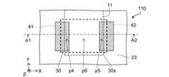
図2は、第1の実施形態に係る半導体装置の一部を例示する模式的断面図である。
図3は、第1の実施形態に係る半導体装置の一部を例示する模式的平面図である。
図2は、図3のA1−A2線断面図である。これらの図は、本実施形態に係る半導体装置に含まれる薄膜トランジスタ110を例示している。FIG. 2 is a schematic cross-sectional view illustrating a part of the semiconductor device according to the first embodiment.
FIG. 3 is a schematic plan view illustrating a part of the semiconductor device according to the first embodiment.
2 is a cross-sectional view taken along line A1-A2 of FIG. These drawings illustrate the
図2及び図3に表したように、第1ゲート電極11は、下地絶縁層160の一部の上に設けられている。第1絶縁層21は、第1ゲート電極11と下地絶縁層160とを覆っている。 As shown in FIGS. 2 and 3, the
第2絶縁層22は、第1絶縁層21の上に設けられる。第2絶縁層22は、第1部分p1と、第2部分p2と、第3部分p3と、を含む。第2部分p2は、X−Y平面(基板150の上面150aに対して平行な平面)内の第1方向(この例では、X軸方向)において第1部分p1と離間する。第3部分p3は、第1部分p1と第2部分p2との間に設けられる。第3部分p3は、第1ゲート電極11の上に位置する。第3部分p3は、第1絶縁層21を介して、第1ゲート電極11と対向する。 The second insulating
半導体層30は、第3部分p3の上において第2絶縁層22に接する。半導体層30は、第4部分p4と、第5部分p5と、第6部分p6と、を含む。第5部分p5は、第1方向(X軸方向)において、第4部分p4と離間する。第6部分p6は、第4部分p4と第5部分p5との間に設けられる。 The
X−Y平面に投影したときに、第4部分p4は、第6部分p6と第1部分p1との間に配置される。X−Y平面に投影したときに、第5部分p5は、第6部分p6と第2部分p2との間に配置される。X−Y平面に投影したときに、第6部分p6は、第3部分p3と重なる。 When projected onto the XY plane, the fourth portion p4 is disposed between the sixth portion p6 and the first portion p1. When projected onto the XY plane, the fifth portion p5 is disposed between the sixth portion p6 and the second portion p2. When projected onto the XY plane, the sixth part p6 overlaps with the third part p3.
第1導電層41は、半導体層30の第4部分p4と接する。この例では、第1導電層41は、第2絶縁層22の第1部分p1と、さらに接する。第2導電層42は、半導体層30の第5部分p5と接する。この例では、第2導電層42は、第2絶縁層22の第2部分p2と、さらに接する。 The first
第1導電層41は、例えば、第3絶縁層23に設けられた第1孔41hに導電材料を埋め込むことにより形成される。第2導電層42は、例えば、第3絶縁層23に設けられた第2孔42hに導電材料を埋め込むことにより形成される。第1孔41hと第2孔42hとは、X軸方向において、互いに離間している。 The first
第3絶縁層23は、半導体層30のうちの、第4部分p4(第1導電層41と接する部分)、及び、第5部分p5(第2導電層42と接する部分)を除く部分を覆う。例えば、第3絶縁層23は、半導体層30の第6部分p6の上面30aを覆う。
図3に例示したように、第3絶縁層23は、半導体層30の側面30s面も覆う。側面30sは、X−Y平面に対して交差する面である。The third insulating
As illustrated in FIG. 3, the third insulating
このように、本実施形態に係る半導体装置210においては、第1配線層171に含まれる下地絶縁層160及び第1ゲート電極11を覆うように、シリコンと窒素とを含む、第1絶縁層21が設けられる。第1絶縁層21には、例えば、窒化シリコン(すなわち、SiNx)などが用いられる。第1絶縁層21は、保護層としての機能が高い。Thus, in the
第2絶縁層22は、半導体層30に接する。第2絶縁層22には、例えば、酸化アルミニウム(例えば、Al2O3、すなわち、AlOx)などが用いられる。第2絶縁層22は、半導体層30に酸素を供給可能である。第2絶縁層22は、水素の半導体層30への侵入を抑制可能である。これにより、例えば、半導体層30において酸素濃度が低くなり、薄膜トランジスタ110における良好なスイッチング特性が低くなる状態が生じた場合にも、良好なスイッチング特性を維持できる。The second insulating
半導体層30は、酸素を含む化合物の第2絶縁層22に接して設けられる。半導体層30と第2絶縁層22との間の界面は、イオン性酸化物の層同士の間に形成される良質な界面となる。これにより、半導体層30において、より良好な特性が得られる。 The
第3絶縁層23には、例えば、酸化シリコン(例えば、SiO2、すなわち、SiOx)などが用いられる。第3絶縁層23は、半導体層30に酸素を供給可能である。これにより、第3絶縁層23からも、半導体層30に酸素を供給でき、良好なスイッチング特性を維持できる。For example, silicon oxide (for example, SiO2 , that is, SiOx ) or the like is used for the third insulating
さらに、本実施形態においては、第2絶縁層22は、半導体層30の加工の際のストッパとして機能する。これにより、酸化物の半導体層30を用いた薄膜トランジスタ110の形成において、実用的なプロセスウインドウが得られる。
本実施形態によれば、集積度が高く実用的な半導体装置が提供できる。Furthermore, in the present embodiment, the second insulating
According to the present embodiment, a practical semiconductor device having a high degree of integration can be provided.
撮像素子などの機能素子155の上に、機能素子155のためのアンプや、制御用のトランジスタを機能素子155の上の層に形成することで、さらなる小型化が実現できる。上の層に設けられるトランジスタとして、薄膜トランジスタを用いることができる。この薄膜トランジスタの半導体層には、CMOSプロセスよりも低温で形成できる半導体材料を用いることが好ましい。この半導体層として、酸化物半導体を用いることができる。 By forming an amplifier for the
酸化物半導体は、例えば、スパッタリング法によって、室温で大面積に均一に成膜でき、300℃〜400℃の比較的低温なプロセス温度が適用できる。さらに、酸化物半導体においては、比較的高い電界効果移動度が得られる。 An oxide semiconductor can be uniformly formed over a large area at room temperature by, for example, a sputtering method, and a relatively low process temperature of 300 ° C. to 400 ° C. can be applied. Further, in the oxide semiconductor, relatively high field effect mobility can be obtained.
本願発明者は、このような酸化物半導体を用いた薄膜トランジスタにおいて、所望の特性が得ることが困難な場合はあることを見出した。
例えば、層間絶縁膜のエッチングストッパ膜として用いられる窒化シリコン層(第1絶縁層21)を薄膜トランジスタ110のゲート絶縁膜として用いる場合、半導体層30を加工する際に、窒化シリコン層がオーバーエッチングされ、所望の形状を形成するのが困難である。これは、半導体層30と窒化シリコン層とにおいて、エッチングの際の選択比が低いためである。窒化シリコン層がオーバーエッチングされると、リークなどの不良が発生し、良好な特性の薄膜トランジスタが得られない。The present inventor has found that it is sometimes difficult to obtain desired characteristics in a thin film transistor using such an oxide semiconductor.
For example, when a silicon nitride layer (first insulating layer 21) used as an etching stopper film for an interlayer insulating film is used as a gate insulating film of the
一方、薄膜トランジスタ110のゲート絶縁膜として、金属酸化物(例えば、Al2O3など)の層を用いると、半導体層30を加工する際の十分な選択比が得られ、金属酸化物の層にダメージを実質的に与えることなく、半導体層30の可能ができる。しかしながら、金属酸化物は、下地絶縁層160に形成される第1ゲート電極11に対するブロック性が低い。このため、例えば、第1ゲート電極11に含まれる金属元素など(例えばCuなど)が、金属酸化物の層を介して、半導体層30中に移動し易い。これにより、半導体層30における特性が劣化する場合がある。On the other hand, when a metal oxide (eg, Al2 O3 ) layer is used as the gate insulating film of the
これに対して、本実施形態においては、下地絶縁層160及び第1ゲート電極11を、ブロック性の高い、窒素を含む第1絶縁層21で覆う。さらに、第1絶縁層21を、半導体層30に対して選択比が高い第2絶縁層22で覆う。 On the other hand, in this embodiment, the
これにより、半導体層30の良好な加工が実現でき、それと同時に、下層からの金属などの移動をブロックできる。そして、第2絶縁層22は、第1絶縁層21から半導体層30へ向けて水素が移動することを抑制できる。 Thereby, the favorable process of the
本実施形態においては、第1絶縁層21には、例えば、窒化シリコン、または、酸窒化シリコンを用いることができる。第2絶縁層22には、酸素を含む金属化合物を用いることができる。 In the present embodiment, for example, silicon nitride or silicon oxynitride can be used for the first insulating
第1絶縁層21として酸窒化シリコンを用い、第2絶縁層22として酸窒化シリコンを用いる場合は、第1絶縁層21における酸素濃度は、第2絶縁層22における酸素濃度よりも低い。これにより、第1絶縁層21において、良好なブロック性が確保できる。そして、第2絶縁層22において、半導体層30に向けての、良好な酸素供給性が確保できる。さらに、第2絶縁層22により、半導体層30への水素の侵入を抑制できる。 When silicon oxynitride is used as the first insulating
すなわち、第1絶縁層21と第2絶縁層22との積層構造を用いることで、第1絶縁層21から半導体層30に向けての水素の拡散が抑制できる。これにより、半導体層30における良好な特性が維持できる。 That is, by using a stacked structure of the first insulating
本実施形態において、第2絶縁層22は、ゲート絶縁膜の一部として機能する。このため、第2絶縁層22における比誘電率は高いことが好ましい。第2絶縁層22として、Al、Ti、Ta、Hf及びZrの少なくともいずれかと、酸素と、を含む第1化合物を用いることで、高い比誘電率が得られる。これにより、薄膜トランジスタ110における駆動能力が向上する。 In the present embodiment, the second insulating
一方、半導体層30の上面(及び側面30s)を覆う第3絶縁層23は、高比誘電率の材料を必ずしも用いなくても良い。第3絶縁層23には、例えば、加工性及び信頼性などを考慮して、酸素を含む適切な材料(例えばSiO2など)を用いることができる。第3絶縁層23に酸素を含む絶縁材料を用いることで、半導体層30における良好な特性が維持できる。On the other hand, the third insulating
本実施形態によれば、高移動度で高信頼性な、実用的な薄膜トランジスタが得られる。 According to this embodiment, a practical thin film transistor with high mobility and high reliability can be obtained.
例えば、半導体装置210の基板150の機能素子155には、撮像素子などが適用される。機能素子155として、CMOSプロセスを用いたCMOSイメージセンサ(撮像素子)を用いることができる。撮像素子において、微細化が進むと、例えば、フォトダイオードの受光面積が減少し、S/N比が悪くなる。本実施形態においては、撮像素子用のアンプまたは制御用のトランジスタを、フォトダイオード上の配線層に形成することで、微細化とS/N比の確保を両立できる。 For example, an imaging element or the like is applied to the
第1絶縁層21の厚さは、例えば、5ナノメートル(nm)以上50nm以下である。 The thickness of the first insulating
第2絶縁層22の厚さは、例えば、50nm以下である。第2絶縁層22の厚さは、10nm以上であることが好ましい。第2絶縁層22の厚さが、100nm以上のときに、エッチングのストッパとしての機能が得易い。過度に薄いと、例えば、ストッパ機能が低下する。 The thickness of the second insulating
本実施形態において、第1ゲート電極11、第1導電層41及び第2導電層42の少なくともいずれかには、アルミニウム、銅、タングステン、タンタル、モリブデン及びチタンの少なくともいずれかを用いることができる。 In the present embodiment, at least one of aluminum, copper, tungsten, tantalum, molybdenum, and titanium can be used for at least one of the
この例では、第1ゲート電極11は、第1ゲート電極11用の第1層11aと、第1ゲート電極11用の第2層11bと、を含む。第2層11bは、第1層11bと積層される。第2層11bは、第1層11aと下地絶縁層160との間に配置される。第1層11aは、アルミニウム、銅、タングステン、タンタル、モリブデン及びチタンの少なくともいずれかの金属を含む。第2層11bには、第1層11aとは異なる材料が用いられる。第2層11bは、タンタル、窒化タンタル及び窒化チタンの少なくともいずれかを含む。 In this example, the
例えば、第1ゲート電極11は、第1ゲート電極11用の第3層11cをさらに含んでも良い。第3層11cは、第1層11aと第2層11bとの間に設けられる。例えば、第1層11aとして、アルミニウム及び銅の少なくともいずれかの金属を用いることができる。第2層11bとして、窒化タンタルを用いることができる。第3層11cとして、タンタルを用いることができる。 For example, the
この例では、第1導電層41は、第1導電層41用の第1層41aと、第1導電層41用の第2層41bと、を含む。第2層41bは、第1層41bと積層される。第2層41bは、第1層41aと第3絶縁層23との間に配置される。第1層41aは、アルミニウム、銅、タングステン、タンタル、モリブデン及びチタンの少なくともいずれかの金属を含む。第2層41bには、第1層41aとは異なる材料が用いられる。第2層41bは、タンタル、窒化タンタル及び窒化チタンの少なくともいずれかを含む。 In this example, the first
例えば、第1導電層41は、第1導電層41用の第3層41cをさらに含んでも良い。第3層41cは、第1層41aと第2層41bとの間に設けられる。例えば、第1層41aとして、アルミニウム及び銅の少なくともいずれかの金属を用いることができる。第2層41bとして、窒化タンタルを用いることができる。第3層41cとして、タンタルを用いることができる。 For example, the first
この例では、第2導電層42は、第2導電層42用の第1層42aと、第2導電層42用の第2層42bと、を含む。第2層42bは、第1層42bと積層される。第2層42bは、第1層42aと第3絶縁層23との間に配置される。第1層42aは、アルミニウム、銅、タングステン、タンタル、モリブデン及びチタンの少なくともいずれかの金属を含む。第2層42bには、第1層42aとは異なる材料が用いられる。第2層42bは、タンタル、窒化タンタル及び窒化チタンの少なくともいずれかを含む。 In this example, the second
例えば、第2導電層42は、第2導電層42用の第3層42cをさらに含んでも良い。第3層42cは、第1層42aと第2層42bとの間に設けられる。例えば、第1層42aとして、アルミニウム及び銅の少なくともいずれかの金属を用いることができる。第2層42bとして、窒化タンタルを用いることができる。第3層42cとして、タンタルを用いることができる。 For example, the second
図4は、第1の実施形態に係る別の半導体装置の一部を例示する模式的断面図である。 図4は、本実施形態に係る別の半導体装置211に含まれる薄膜トランジスタ111を例示している。 FIG. 4 is a schematic cross-sectional view illustrating a part of another semiconductor device according to the first embodiment. FIG. 4 illustrates a
図4に表したように、半導体装置211における薄膜トランジスタ111においては、第2絶縁層22は、半導体層30の第6部分p6の上に設けられる部分22pをさらに含む。第2絶縁層22は、例えば、第4部分p4及び第5部分p5を除いて、半導体層30を覆う。例えば、第2絶縁層22は、半導体層30の側面30sを覆う。第3絶縁層23は、第2絶縁層22を介して、半導体層30を覆う。これ以外は、薄膜トランジスタ110と同様とすることができるので、説明を省略する。 As shown in FIG. 4, in the
半導体装置211においても、集積度が高く実用的な半導体装置が提供できる。半導体装置211においては、第2絶縁層22は、半導体層30の下面だけでなく、半導体層30の上面及び側面30sを覆う。同じ材料で半導体層30を覆うことで、薄膜トランジスタ111において、より安定した特性が得られる。 Also in the
図5は、第1の実施形態に係る別の半導体装置の一部を例示する模式的断面図である。 図5は、本実施形態に係る別の半導体装置212に含まれる薄膜トランジスタ112を例示している。 FIG. 5 is a schematic cross-sectional view illustrating a part of another semiconductor device according to the first embodiment. FIG. 5 illustrates a
図5に表したように、半導体装置212における薄膜トランジスタ112は、ダブルゲート構造を有する。すなわち、薄膜トランジスタ112は、第2ゲート電極12をさらに含む。これ以外は、薄膜トランジスタ110と同様とすることができるので、説明を省略する。半導体装置212においては、第1配線層171の配線の一部が、薄膜トランジスタ112の第1ゲート電極11として用いられ、第2配線層172の配線の一部が、第2ゲート電極12として用いられる。 As illustrated in FIG. 5, the
第2ゲート電極12は、半導体層30の第6部分p6の上に設けられる。第3絶縁層23は、第6部分p6と第2ゲート電極12との間に設けられた部分23pを含む。第2ゲート電極12は、例えば、第3絶縁層23に設けられた第3孔43hに導電材料を埋め込むことにより形成される。第3孔43hは、第1孔41hと第2孔42hとの間に設けられる。 The
薄膜トランジスタ112は、ダブルゲート構造を有しているため、より安定した特性が得られる。半導体装置212においても、集積度が高く実用的な半導体装置が提供できる。 Since the
第2ゲート電極12は、アルミニウム、銅、タングステン、タンタル、モリブデン及びチタンの少なくともいずれかを含むことができる。 The
この例では、第2ゲート電極12は、第2ゲート電極12用の第1層12aと、第2ゲート電極12用の第2層12bと、を含む。第2層12bは、第1層12bと積層される。第2層12bは、第1層12aと第3絶縁層23との間に配置される。第1層12aは、アルミニウム、銅、タングステン、タンタル、モリブデン及びチタンの少なくともいずれかの金属を含む。第2層12bには、第1層12aとは異なる材料が用いられる。第2層12bは、タンタル、窒化タンタル及び窒化チタンの少なくともいずれかを含む。 In this example, the
例えば、第2ゲート電極12は、第2ゲート電極12用の第3層12cをさらに含んでも良い。第3層12cは、第1層12aと第2層12bとの間に設けられる。例えば、第1層12aとして、アルミニウム及び銅の少なくともいずれかの金属を用いることができる。第2層12bとして、窒化タンタルを用いることができる。第3層12cとして、タンタルを用いることができる。 For example, the
第2ゲート電極12が設けられる場合、配線50(図1参照)は、第2ゲート電極12と接続されても良い。すなわち、半導体装置212は、例えば、Z軸方向(例えば、基板150の上面150aに対して交差する方向)に沿って、第3絶縁層23の少なくとも一部と、下地絶縁層160と、を貫通する第2ゲート電極用の配線50をさらに含んでも良い。配線50は、例えば、機能素子155と第2ゲート電極12とを電気的に接続する。 When the
図6は、第1の実施形態に係る別の半導体装置の一部を例示する模式的断面図である。 図6は、本実施形態に係る別の半導体装置213に含まれる薄膜トランジスタ113を例示している。 FIG. 6 is a schematic cross-sectional view illustrating a part of another semiconductor device according to the first embodiment. FIG. 6 illustrates a
図6に表したように、半導体装置213における薄膜トランジスタ113においては、第2絶縁層22は、半導体層30の第6部分p6の上に設けられる部分22pをさらに含む。すなわち、第2絶縁層22は、第6部分p6と第2ゲート電極12との間に設けられた部分22pを含む。これ以外は、薄膜トランジスタ112と同様とすることができるので、説明を省略する。 As shown in FIG. 6, in the
第2絶縁層22は、例えば、第4部分p4及び第5部分p5を除いて、半導体層30を覆う。例えば、第2絶縁層22は、半導体層30の側面30sを覆う。第3絶縁層23は、第2絶縁層22を介して、半導体層30を覆う。 For example, the second insulating
半導体装置213においても、集積度が高く実用的な半導体装置が提供できる。半導体装置213においては、第2絶縁層22は、半導体層30の下面だけでなく、半導体層30の上面及び側面30sを覆う。同じ材料で半導体層30を覆う。さらに、ダブルゲート構造が適用される。薄膜トランジスタ113において、より安定した特性が得られる。 The
(第2の実施形態)
本実施形態においては、トップゲート構造の薄膜トランジスタが設けられる。
図7は、第2の実施形態に係る半導体装置の一部を例示する模式的断面図である。
図7は、本実施形態に係る半導体装置220に含まれる薄膜トランジスタ120を例示している。(Second Embodiment)
In this embodiment, a thin film transistor having a top gate structure is provided.
FIG. 7 is a schematic cross-sectional view illustrating a part of the semiconductor device according to the second embodiment.
FIG. 7 illustrates a
半導体装置220においても、図1に関して説明した基板150が設けられる。この場合も、基板150は、機能素子155を含み、上面150aを有する。半導体装置220においても、上面150aの上に下地絶縁層160が設けられる。さらに、配線50を設けても良い。基板150、下地絶縁層160及び配線50に関しては、半導体装置210と同様とすることができるので説明を省略する。半導体装置220においては、第2配線層172の配線の一部が、薄膜トランジスタ120の第1ゲート電極11として用いられる。以下、下地絶縁層160の上に位置する部分について説明する。 The
半導体装置220は、基板150、下地絶縁層160及び配線50に加えて、第1絶縁層21と、第2絶縁層22と、半導体層30と、ゲート絶縁層16と、第1ゲート電極11と、第1導電層41と、第2導電層42と、第3絶縁層23と、を含む。半導体層30、ゲート絶縁層16、第1ゲート電極11、第1導電層41、第2導電層42及び第3絶縁層23は、例えば、薄膜トランジスタ120に含まれる。 The
第1絶縁層21は、下地絶縁層160の上に設けられる。第1絶縁層21は、シリコンと窒素とを含む。第1絶縁層21には、例えば、窒化シリコン、または、酸窒化シリコンが用いられる。 The first insulating
第2絶縁層22は、第1絶縁層21の上に設けられる。第2絶縁層22は、第1部分p1と、第2部分p2と、第3部分p3と、を含む。第2部分p2は、X−Y平面(上面150aに対して平行な平面)内の第1方向(例えば、X軸方向)において、第1部分p1と離間する。第3部分p3は、第1部分p1と第2部分p2との間に設けられる。この場合も、第2絶縁層22は、Al、Ti、Ta、Hf及びZrの少なくともいずれかと、酸素と、を含む。 The second insulating
半導体層30は、第3部分p3の上において第2絶縁層22に接する。半導体層30は、第4部分p4と、第5部分p5と、第6部分p6と、を含む。第5部分p5は、第1方向(X軸方向)において、第4部分p4と離間する。第6部分p6は、第4部分p4と第5部分p5との間に設けられる。半導体層30には、インジウム、ガリウム及び亜鉛の少なくともいずれかを含む酸化物が用いられる。 The
この場合も、X−Y平面に投影したときに、第4部分p4は、第6部分p6と第1部分p1との間に配置される。X−Y平面に投影したときに、第5部分p5は、第6部分p6と第2部分p2との間に配置される。X−Y平面に投影したときに、第6部分p6は、第3部分p3と重なる。 Also in this case, when projected onto the XY plane, the fourth portion p4 is disposed between the sixth portion p6 and the first portion p1. When projected onto the XY plane, the fifth portion p5 is disposed between the sixth portion p6 and the second portion p2. When projected onto the XY plane, the sixth part p6 overlaps with the third part p3.
ゲート絶縁層16は、半導体層30の第6部分p6の上に設けられる。ゲート絶縁層16は、金属と酸素とを含む。ゲート絶縁層16は、例えば、Al、Ti、Ta、Hf及びZrの少なくともいずれかと、酸素と、を含むことができる。 The
第1ゲート電極11は、ゲート絶縁層16の上に設けられる。すなわち、半導体層30の第6部分p6と、第1ゲート電極11と、の間に、ゲート絶縁層16が設けられる。 The
第1導電層41は、第1部分p1と第4部分p4と接する。第2導電層42は、第2部分p2と第5部分p5と接する。 The first
第3絶縁層23は、半導体層30のうちの、第4部分p4及び第5部分p5を除く部分を覆う。第3絶縁層23は、ゲート絶縁層16と連続的でも良い。第3絶縁層23は、ゲート絶縁層16を介して、半導体層30の第6部分p6を覆っても良い。第3絶縁層23は、半導体層30の側面30sをさらに覆っても良い。第3絶縁層23は、Si、Al、Ti、Ta、Hf及びZrの少なくともいずれかと、酸素と、を含む。 The third insulating
本実施形態においても、下地絶縁層160及び第1ゲート電極11を、ブロック性の高い、窒素を含む第1絶縁層21で覆う。さらに、第1絶縁層21を、半導体層30に対して選択比が高い第2絶縁層22で覆う。これにより、半導体層30の良好な加工が実現でき、それと同時に、下層からの金属などの移動をブロックできる。さらに、第2絶縁層22により、第1絶縁層21から半導体層30に向けての水素の移動を抑制できる。さらに、第2絶縁層22において、半導体層30に向けての、良好な酸素供給性が確保できる。これにより、半導体層30における良好な特性が維持できる。 Also in this embodiment, the
本実施形態において、ゲート絶縁層16の比誘電率は高いことが好ましい。ゲート絶縁層16として、Al、Ti、Ta、Hf及びZrの少なくともいずれかと、酸素と、を含む化合物を用いることで、高い比誘電率が得られる。これにより、薄膜トランジスタ120における駆動能力が向上する。 In the present embodiment, it is preferable that the dielectric constant of the
本実施形態によれば、高移動度で高信頼性な、実用的な薄膜トランジスタが得られる。本実施形態においても、集積度が高く実用的な半導体装置が提供できる。 According to this embodiment, a practical thin film transistor with high mobility and high reliability can be obtained. Also in this embodiment, a practical semiconductor device having a high degree of integration can be provided.
この例において、第3絶縁層23の材料をゲート絶縁層16の材料と同じにしても良い。この場合には、第3絶縁層23とゲート絶縁層16とが連続的であり、境界が観測されない。この材料の絶縁層のうちで、半導体層30と第1導電層41との間に位置する部分が、ゲート絶縁層16となる。それ例外の部分が、第3絶縁層23となる。 In this example, the material of the third insulating
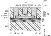
図8は、第2の実施形態に係る別の半導体装置の一部を例示する模式的断面図である。 図8は、本実施形態に係る半導体装置221に含まれる薄膜トランジスタ121を例示している。
図8に表したように、薄膜トランジスタ121においては、ゲート絶縁層16は、第2絶縁層22と連続的である。例えば、ゲート絶縁層16の材料は、第2絶縁層22の材料と同じである。例えば、ゲート絶縁層16及び第2絶縁層22には、Al、Ti、Ta、Hf及びZrの少なくともいずれかと、酸素と、を含む化合物が用いられる。高い比誘電率と共に、高いエッチングストッパ性が得られる。FIG. 8 is a schematic cross-sectional view illustrating a part of another semiconductor device according to the second embodiment. FIG. 8 illustrates a
As shown in FIG. 8, in the
半導体層30の下面と上面とが同じ材料で覆われることから、薄膜トランジスタ121においては、より安定した特性が得られる。半導体装置211においても、集積度が高く実用的な半導体装置が提供できる。 Since the lower surface and the upper surface of the
(第3の実施形態)
本実施形態は、第1の実施形態に係る半導体装置の製造方法に係る。
図9は、第3の実施形態に係る半導体装置の製造方法を例示するフローチャート図である。
図10(a)〜図10(c)は、第3の実施形態に係る半導体装置の製造方法を例示する工程順模式的断面図である。
図9に表したように、本製造方法では、機能素子155を含み上面150aを有する基板150のその上面150aの上に、下地絶縁層160を形成する(ステップS110)。(Third embodiment)
The present embodiment relates to a method for manufacturing a semiconductor device according to the first embodiment.
FIG. 9 is a flowchart illustrating the method for manufacturing the semiconductor device according to the third embodiment.
FIG. 10A to FIG. 10C are schematic cross-sectional views in order of the processes, illustrating the method for manufacturing the semiconductor device according to the third embodiment.
As shown in FIG. 9, in this manufacturing method, the
下地絶縁層160の一部の上に、第1ゲート電極11を形成する(ステップS120)。 The
第1ゲート電極11と下地絶縁層160とを覆うように、シリコンと窒素とを含む第1絶縁層21を形成する(ステップS130)。 A first insulating
第1絶縁層21の上に、Al、Ti、Ta、Hf及びZrの少なくともいずれかと、酸素と、を含む第2絶縁層22を形成する(ステップS140)。 A second insulating
図10(a)に表したように、第2絶縁層22の上に、インジウム、ガリウム及び亜鉛の少なくともいずれかを含む酸化物の半導体膜30fを形成する。 As illustrated in FIG. 10A, an
図10(b)に表したように、第2絶縁層22をストッパとして用いて半導体膜30fを加工して、半導体膜30fから半導体層30を形成する(ステップS150)。半導体膜30fの加工には、例えば、ドライエッチングが用いられる。ドライエッチングにおいては、例えば塩素を含むガスが用いられる。三塩化ホウ素を含むガスを用いても良い。 As shown in FIG. 10B, the
半導体層30の上及び第2絶縁層22の上の上に、Si、Al、Ti、Ta、Hf及びZrの少なくともいずれかと、酸素と、を含む第3絶縁層23を形成する(ステップS160)。 A third insulating
図10(c)に表したように、第3絶縁層23の上面から、半導体層30に到達する第1孔41hと、半導体層30に到達し第1孔41hから離間する第2孔42hと、を形成する(ステップS170)。第1孔41h及び第2孔42hの形成においては、例えば、第2絶縁層22がストッパとして用いられる。第1孔41h及び第2孔42hの形成には、例えば、ドライエッチングが用いられる。ドライエッチングにおいては、例えば、四フッ化メタン、トリフルオロメタン及び酸素の少なくともいずれかを含むガスが用いられる。 As shown in FIG. 10C, the
第1孔41hと第2孔42hに導電材料を埋め込む(ステップS180)。第1孔41hに埋め込まれた導電材料により、第1導電層41が形成される。第2孔42hに埋め込まれた導電材料により、第2導電層42が形成される。以上により、半導体層30を含む薄膜トランジスタ(例えば、薄膜トランジスタ110)が形成される。 A conductive material is embedded in the
上記の第1孔41h及び第2孔42hの形成(ステップS170)は、第3絶縁層23の上面から、半導体層30から離間する第3孔43hを形成することを含んでも良い。第3孔42hは、第1孔41hと第2孔42hとの間に形成される。そして、導電材料の埋め込み(ステップS180)は、第3孔43hに導電材料を埋め込むことを含むことができる。これにより、第2ゲート電極12が形成できる。
本実施形態に係る製造方法によれば、高集積度で実用的な半導体装置の製造方法が提供できる。The formation of the
According to the manufacturing method according to the present embodiment, a highly integrated and practical semiconductor device manufacturing method can be provided.
図10(c)に表したように、本実施形態において、配線50のための孔(配線孔50h)をさらに設けても良い。すなわち、第1孔41h及び第2孔42hの形成(ステップS170)は、機能素子155と薄膜トランジスタとを電気的に接続する配線50の少なくとも一部が形成される配線孔50hの形成を含むことができる。そして、導電材料の埋め込み(ステップ180)は、配線孔50hに導電材料を埋め込むことを含むことができる。これにより、配線50の少なくとも一部が形成できる。 As shown in FIG. 10C, in the present embodiment, a hole (
(第4の実施形態)
本実施形態は、第2の実施形態に係る半導体装置の製造方法に係る。
図11は、第4の実施形態に係る半導体装置の製造方法を例示するフローチャート図である。
図12(a)〜図12(c)は、第4の実施形態に係る半導体装置の製造方法を例示する工程順模式的断面図である。
図11に表したように、本製造方法では、機能素子155を含み上面150aを有する基板150の上面150aの上に下地絶縁層160を形成する(ステップS110)。(Fourth embodiment)
The present embodiment relates to a method for manufacturing a semiconductor device according to the second embodiment.
FIG. 11 is a flowchart illustrating the method for manufacturing the semiconductor device according to the fourth embodiment.
FIG. 12A to FIG. 12C are schematic cross-sectional views in order of the processes, illustrating the method for manufacturing the semiconductor device according to the fourth embodiment.
As shown in FIG. 11, in this manufacturing method, the
下地絶縁層160の上に、シリコンと窒素とを含む第1絶縁層21を形成する(ステップS130)。 A first insulating
第1絶縁層21の上に、Al、Ti、Ta、Hf及びZrの少なくともいずれかと酸素とを含む第2絶縁層22を形成する(ステップS140)。 A second insulating
図12(a)に表したように、第2絶縁層22の上に、インジウム、ガリウム及び亜鉛の少なくともいずれかを含む酸化物の半導体膜30fを形成する。 As illustrated in FIG. 12A, an
図12(b)に表したように、第2絶縁層22をストッパとして用いて、半導体膜30fを加工して、半導体膜30fから半導体層30を形成する(ステップS150)。この場合も、半導体膜30fの加工には、例えば、ドライエッチングが用いられる。ドライエッチングにおいては、例えば塩素を含むガスが用いられる。三塩化ホウ素を含むガスを用いても良い。 As shown in FIG. 12B, the
半導体層30の上、及び、第2絶縁層22の上に、Si、Al、Ti、Ta、Hf及びZrの少なくともいずれかと酸素とを含む第3絶縁層23を形成する(ステップS160)。例えば、第3絶縁層23のうちの半導体層30の上の部分が、ゲート絶縁層16となる。 A third insulating
図12(c)に表したように、第3絶縁層23の上面から、半導体層30に到達する第1孔41hと、半導体層30に到達し第1孔41hから離間する第2孔42hと、第1孔41hと第2孔42hとの間において半導体層30から離間する第3孔42hと、を形成する(ステップS171)。第1孔41h、第2孔42h及び第3孔50hの形成には、例えば、ドライエッチングが用いられる。この場合も、ドライエッチングにおいては、例えば、四フッ化メタン、トリフルオロメタン及び酸素の少なくともいずれかを含むガスが用いられる。 As shown in FIG. 12C, the
第1孔41h、第2孔42h及び第3孔43hに導電材料を埋め込む(ステップS180)。第1孔41hに埋め込まれた導電材料により、第1導電層41が形成される。第2孔42hに埋め込まれた導電材料により、第2導電層42が形成される。第3孔43hに埋め込まれた導電材料により、第1ゲート電極11が形成される。以上により、半導体層30を含む薄膜トランジスタ(例えば、薄膜トランジスタ120)が形成される。 A conductive material is embedded in the
本実施形態に係る製造方法によれば、高集積度で実用的な半導体装置の製造方法が提供できる。 According to the manufacturing method according to the present embodiment, a highly integrated and practical semiconductor device manufacturing method can be provided.
図12(c)に表したように、この場合も、第1孔41h及び第2孔42hの形成(ステップS171)は、機能素子155と薄膜トランジスタとを電気的に接続する配線50の少なくとも一部が形成される配線孔50hの形成を含むことができる。そして、導電材料の埋め込み(ステップ180)は、配線孔50hに導電材料を埋め込むことを含むことができる。これにより、配線50の少なくとも一部が形成できる。 As shown in FIG. 12C, also in this case, the formation of the
第1〜第4の実施形態において、第2絶縁層22及び第3絶縁層23に酸化シリコンを用いる場合、これらの層の少なくともいずれかにTEOS膜を用いても良い。第2絶縁層22及び第3絶縁層23の少なくともいずれかに、ポーラス膜を用いても良い。ポーラス膜においては、例えばSiOCが用いられる。ポーラス膜を用いることで、例えば、配線間の寄生容量を低減できる。 In the first to fourth embodiments, when silicon oxide is used for the second insulating
実施形態によれば、高集積度で実用的な半導体装置及びその製造方法が提供できる。 According to the embodiment, a highly integrated and practical semiconductor device and a manufacturing method thereof can be provided.
なお、本願明細書において、「垂直」及び「平行」は、厳密な垂直及び厳密な平行だけではなく、例えば製造工程におけるばらつきなどを含むものであり、実質的に垂直及び実質的に平行であれば良い。 In the present specification, “vertical” and “parallel” include not only strict vertical and strict parallel but also include, for example, variations in the manufacturing process, and may be substantially vertical and substantially parallel. It ’s fine.
以上、具体例を参照しつつ、本発明の実施の形態について説明した。しかし、本発明は、これらの具体例に限定されるものではない。例えば、半導体装置に含まれる基板、機能措置、下地絶縁層、第1ゲート電極、第2ゲート電極、第1〜第3絶縁層、ゲート絶縁層、第1導電層、第2導電層、配線、第1〜第3配線、及び、層間絶縁層などの各要素の具体的な構成に関しては、当業者が公知の範囲から適宜選択することにより本発明を同様に実施し、同様の効果を得ることができる限り、本発明の範囲に包含される。 The embodiments of the present invention have been described above with reference to specific examples. However, the present invention is not limited to these specific examples. For example, a substrate included in a semiconductor device, a functional measure, a base insulating layer, a first gate electrode, a second gate electrode, first to third insulating layers, a gate insulating layer, a first conductive layer, a second conductive layer, a wiring, With regard to the specific configuration of each element such as the first to third wirings and the interlayer insulating layer, a person skilled in the art appropriately implements the present invention by appropriately selecting from a known range, and obtains the same effect. Is included in the scope of the present invention as long as possible.
また、各具体例のいずれか2つ以上の要素を技術的に可能な範囲で組み合わせたものも、本発明の要旨を包含する限り本発明の範囲に含まれる。 Moreover, what combined any two or more elements of each specific example in the technically possible range is also included in the scope of the present invention as long as the gist of the present invention is included.
その他、本発明の実施の形態として上述した半導体装置及びその製造方法を基にして、当業者が適宜設計変更して実施し得る全ての半導体装置及びその製造方法も、本発明の要旨を包含する限り、本発明の範囲に属する。 In addition, all semiconductor devices and manufacturing methods that can be implemented by those skilled in the art based on the above-described semiconductor device and manufacturing method described above as embodiments of the present invention include the gist of the present invention. As long as it belongs to the scope of the present invention.
その他、本発明の思想の範疇において、当業者であれば、各種の変更例及び修正例に想到し得るものであり、それら変更例及び修正例についても本発明の範囲に属するものと了解される。 In addition, in the category of the idea of the present invention, those skilled in the art can conceive of various changes and modifications, and it is understood that these changes and modifications also belong to the scope of the present invention. .
本発明のいくつかの実施形態を説明したが、これらの実施形態は、例として提示したものであり、発明の範囲を限定することは意図していない。これら新規な実施形態は、その他の様々な形態で実施されることが可能であり、発明の要旨を逸脱しない範囲で、種々の省略、置き換え、変更を行うことができる。これら実施形態やその変形は、発明の範囲や要旨に含まれるとともに、特許請求の範囲に記載された発明とその均等の範囲に含まれる。 Although several embodiments of the present invention have been described, these embodiments are presented by way of example and are not intended to limit the scope of the invention. These novel embodiments can be implemented in various other forms, and various omissions, replacements, and changes can be made without departing from the scope of the invention. These embodiments and modifications thereof are included in the scope and gist of the invention, and are included in the invention described in the claims and the equivalents thereof.
11…第1ゲート電極、 11a、11b、11c…第1、第2、第3層、 12…第2ゲート電極、 12a、12b、12c…第1、第2、第3層、 16…ゲート絶縁層、 21…第1絶縁層、 22…第2絶縁層、 22p…部分、 23…第3絶縁層、 23p…部分、 30…半導体層、 30a…上面、 30f…半導体膜、 30s…側面、 41…第1導電層、 41a、41b、41c…第1、第2、第3層、 41h…第1孔、 42…第2導電層、 42a、42b、42c…第1、第2、第3層、 42h…第2孔、 43h…第3孔、 50…配線、 50h…配線孔、 51…第1配線、 52…第2配線、 52a…上側層、 52b…下側層、 53…第3配線、 53a…上側層、 53b…下側層、 110、111、112、113、120、121…薄膜トランジスタ、 150…基板、 150a…上面、 150b…下面、 150i…層間絶縁層、 155…機能素子、 156…撮像部、 160…下地絶縁層、 171…第1配線層、 171i…第1層間絶縁層、 172…第2配線層、 172i…上層絶縁層、 210、211、212、213、220、221…半導体装置、 p1〜p6…第1〜第6部分 DESCRIPTION OF
Claims (11)
Translated fromJapanese前記上面の上に設けられた下地絶縁層と、
前記下地絶縁層の一部の上に設けられた第1ゲート電極と、
前記第1ゲート電極と前記下地絶縁層とを覆いシリコンと窒素とを含む第1絶縁層と、
前記第1絶縁層の上に設けられ、第1部分と、前記上面に対して平行な平面内の第1方向において前記第1部分と離間する第2部分と、前記第1部分と前記第2部分との間に設けられ前記第1ゲート電極の上に位置する第3部分と、を含み、Al、Ti、Ta、Hf及びZrの少なくともいずれかと酸素とを含む第2絶縁層と、
前記第3部分の上において前記第2絶縁層に接し、第4部分と、前記第1方向において前記第4部分と離間する第5部分と、前記第4部分と前記第5部分との間に設けられた第6部分と、を含み、前記上面に対して平行な平面に投影したときに、前記第4部分は、前記第6部分と前記第1部分との間に配置され、前記第5部分は、前記第6部分と前記第2部分との間に配置され、In、Ga及びZnの少なくともいずれかを含む酸化物の半導体層と、
前記第4部分と接する第1導電層と、
前記第5部分と接する第2導電層と、
前記半導体層のうちの、前記第4部分及び前記第5部分を除く部分を覆い、Si、Al、Ti、Ta、Hf及びZrの少なくともいずれかと酸素とを含む第3絶縁層と、
を含む薄膜トランジスタと、
を備えた半導体装置。A substrate including a functional element and having an upper surface;
A base insulating layer provided on the upper surface;
A first gate electrode provided on a portion of the base insulating layer;
A first insulating layer covering silicon and nitrogen covering the first gate electrode and the base insulating layer;
A first portion; a second portion spaced apart from the first portion in a first direction in a plane parallel to the upper surface; the first portion; and the second portion. A third portion disposed between the first gate electrode and the first gate electrode, and a second insulating layer containing at least one of Al, Ti, Ta, Hf, and Zr and oxygen,
On the third portion, in contact with the second insulating layer, between the fourth portion, the fifth portion separated from the fourth portion in the first direction, and between the fourth portion and the fifth portion. The fourth portion is disposed between the sixth portion and the first portion when projected onto a plane parallel to the upper surface, and the fifth portion is provided. The portion is disposed between the sixth portion and the second portion, and an oxide semiconductor layer including at least one of In, Ga, and Zn;
A first conductive layer in contact with the fourth portion;
A second conductive layer in contact with the fifth portion;
A third insulating layer covering at least one of Si, Al, Ti, Ta, Hf, and Zr and oxygen, covering a portion of the semiconductor layer excluding the fourth portion and the fifth portion;
A thin film transistor comprising:
A semiconductor device comprising:
前記上面の上に設けられた下地絶縁層と、
前記下地絶縁層の上に設けられたシリコンと窒素とを含む第1絶縁層と、
前記第1絶縁層の上に設けられ、第1部分と、前記上面に対して平行な平面内の第1方向において前記第1部分と離間する第2部分と、前記第1部分と前記第2部分との間に設けられた第3部分と、を含み、Al、Ti、Ta、Hf及びZrの少なくともいずれかと酸素とを含む第2絶縁層と、
前記第3部分の上において前記第2絶縁層に接し、第4部分と、前記第1方向において前記第4部分と離間する第5部分と、前記第4部分と前記第5部分との間に設けられた第6部分と、を含み、前記第4部分は、前記第6部分と前記第1部分との間に配置され、前記第5部分は、前記第6部分と前記第2部分との間に配置され、インジウム、ガリウム及び亜鉛の少なくともいずれかを含む酸化物の半導体層と、
前記第6部分の上に設けられ金属と酸素とを含むゲート絶縁層と、
前記ゲート絶縁層の上に設けられた第1ゲート電極と、
前記第4部分と接する第1導電層と、
前記第5部分と接する第2導電層と、
前記半導体層のうちの、前記第4部分及び前記第5部分を除く部分を覆い、Si、Al、Ti、Ta、Hf及びZrの少なくともいずれかと酸素とを含む第3絶縁層と、
を含む薄膜トランジスタと、
を備えた半導体装置。A substrate including a functional element and having an upper surface;
A base insulating layer provided on the upper surface;
A first insulating layer including silicon and nitrogen provided on the base insulating layer;
A first portion; a second portion spaced apart from the first portion in a first direction in a plane parallel to the upper surface; the first portion; and the second portion. A third part provided between the two parts, and a second insulating layer containing at least one of Al, Ti, Ta, Hf and Zr and oxygen,
On the third portion, in contact with the second insulating layer, between the fourth portion, the fifth portion separated from the fourth portion in the first direction, and between the fourth portion and the fifth portion. A sixth portion provided, wherein the fourth portion is disposed between the sixth portion and the first portion, and the fifth portion is formed between the sixth portion and the second portion. An oxide semiconductor layer disposed between and comprising at least one of indium, gallium, and zinc;
A gate insulating layer provided on the sixth portion and containing metal and oxygen;
A first gate electrode provided on the gate insulating layer;
A first conductive layer in contact with the fourth portion;
A second conductive layer in contact with the fifth portion;
A third insulating layer covering at least one of Si, Al, Ti, Ta, Hf, and Zr and oxygen, covering a portion of the semiconductor layer excluding the fourth portion and the fifth portion;
A thin film transistor comprising:
A semiconductor device comprising:
前記第2絶縁層は、酸化アルミニウムを含む請求項1〜7のいずれか1つに記載の半導体装置。The first insulating layer includes silicon nitride;
The semiconductor device according to claim 1, wherein the second insulating layer includes aluminum oxide.
前記下地絶縁層の一部の上に第1ゲート電極を形成し、
前記第1ゲート電極と前記下地絶縁層とを覆うように、シリコンと窒素とを含む第1絶縁層を形成し、
前記第1絶縁層の上にAl、Ti、Ta、Hf及びZrの少なくともいずれかと酸素とを含む第2絶縁層を形成し、
前記第2絶縁層の上に、インジウム、ガリウム及び亜鉛の少なくともいずれかを含む酸化物の半導体膜を形成して、前記第2絶縁層をストッパとして用いて前記半導体膜を加工して前記半導体膜から半導体層を形成し、
前記半導体層の上及び前記第2絶縁層の上に、Si、Al、Ti、Ta、Hf及びZrの少なくともいずれかと酸素とを含む第3絶縁層を形成し、
前記第3絶縁層の上面から、前記半導体層に到達する第1孔と、前記半導体層に到達し前記第1孔から離間する第2孔と、を形成し、
前記第1孔及び前記第2孔に導電材料を埋め込んで、前記半導体層を含む薄膜トランジスタを形成することを含む半導体装置の製造方法。Forming a base insulating layer on the upper surface of the substrate including the functional element and having the upper surface;
Forming a first gate electrode on a portion of the base insulating layer;
Forming a first insulating layer containing silicon and nitrogen so as to cover the first gate electrode and the base insulating layer;
Forming a second insulating layer containing at least one of Al, Ti, Ta, Hf and Zr and oxygen on the first insulating layer;
An oxide semiconductor film containing at least one of indium, gallium, and zinc is formed on the second insulating layer, and the semiconductor film is processed using the second insulating layer as a stopper. Forming a semiconductor layer from
Forming a third insulating layer containing at least one of Si, Al, Ti, Ta, Hf, and Zr and oxygen on the semiconductor layer and the second insulating layer;
Forming a first hole reaching the semiconductor layer from a top surface of the third insulating layer and a second hole reaching the semiconductor layer and spaced from the first hole;
A method for manufacturing a semiconductor device, comprising: embedding a conductive material in the first hole and the second hole to form a thin film transistor including the semiconductor layer.
Priority Applications (6)
| Application Number | Priority Date | Filing Date | Title |
|---|---|---|---|
| JP2013061045AJP2014187181A (en) | 2013-03-22 | 2013-03-22 | Semiconductor device and manufacturing method of the same |
| US14/173,028US20140284593A1 (en) | 2013-03-22 | 2014-02-05 | Semiconductor device and method for manufacturing the same |
| EP14154293.6AEP2782138A3 (en) | 2013-03-22 | 2014-02-07 | Semiconductor device and method for manufacturing the same |
| TW103104257ATW201501326A (en) | 2013-03-22 | 2014-02-10 | Semiconductor device and method of manufacturing same |
| KR1020140024529AKR20140115969A (en) | 2013-03-22 | 2014-02-28 | Semiconductor device and method for manufacturing the same |
| CN201410074863.3ACN104064537A (en) | 2013-03-22 | 2014-03-03 | Semiconductor device and manufacturing method thereof |
Applications Claiming Priority (1)
| Application Number | Priority Date | Filing Date | Title |
|---|---|---|---|
| JP2013061045AJP2014187181A (en) | 2013-03-22 | 2013-03-22 | Semiconductor device and manufacturing method of the same |
Publications (2)
| Publication Number | Publication Date |
|---|---|
| JP2014187181Atrue JP2014187181A (en) | 2014-10-02 |
| JP2014187181A5 JP2014187181A5 (en) | 2014-11-13 |
Family
ID=50064503
Family Applications (1)
| Application Number | Title | Priority Date | Filing Date |
|---|---|---|---|
| JP2013061045APendingJP2014187181A (en) | 2013-03-22 | 2013-03-22 | Semiconductor device and manufacturing method of the same |
Country Status (6)
| Country | Link |
|---|---|
| US (1) | US20140284593A1 (en) |
| EP (1) | EP2782138A3 (en) |
| JP (1) | JP2014187181A (en) |
| KR (1) | KR20140115969A (en) |
| CN (1) | CN104064537A (en) |
| TW (1) | TW201501326A (en) |
Cited By (6)
| Publication number | Priority date | Publication date | Assignee | Title |
|---|---|---|---|---|
| JP2016167060A (en)* | 2015-03-03 | 2016-09-15 | 群創光電股▲ふん▼有限公司Innolux Corporation | Display panel and display device |
| JP2017120904A (en)* | 2015-12-28 | 2017-07-06 | 株式会社半導体エネルギー研究所 | Electrode, semiconductor device, semiconductor wafer, module, electronic device and manufacturing method thereof |
| JP2019091902A (en)* | 2015-01-26 | 2019-06-13 | 株式会社半導体エネルギー研究所 | Semiconductor device |
| JP2020102649A (en)* | 2015-03-13 | 2020-07-02 | 株式会社半導体エネルギー研究所 | Semiconductor device |
| JP2021119600A (en)* | 2015-02-20 | 2021-08-12 | 株式会社半導体エネルギー研究所 | Semiconductor device |
| JP2023071789A (en)* | 2015-03-30 | 2023-05-23 | 株式会社半導体エネルギー研究所 | Manufacturing method of semiconductor device |
Families Citing this family (5)
| Publication number | Priority date | Publication date | Assignee | Title |
|---|---|---|---|---|
| TW201611298A (en)* | 2014-09-12 | 2016-03-16 | 中華映管股份有限公司 | Double film transistor and manufacturing method thereof |
| WO2017105515A1 (en)* | 2015-12-18 | 2017-06-22 | Intel Corporation | Stacked transistors |
| JP2018157101A (en)* | 2017-03-17 | 2018-10-04 | 東芝メモリ株式会社 | Transistor, memory, and method of manufacturing transistor |
| CN108198864B (en)* | 2018-01-05 | 2021-12-03 | 京东方科技集团股份有限公司 | Thin film transistor, manufacturing method thereof, array substrate and display device |
| KR20210133524A (en) | 2020-04-29 | 2021-11-08 | 삼성전자주식회사 | Interconnection structure and Semiconductor package including the same |
Citations (9)
| Publication number | Priority date | Publication date | Assignee | Title |
|---|---|---|---|---|
| JP2010141230A (en)* | 2008-12-15 | 2010-06-24 | Renesas Electronics Corp | Semiconductor device, and method of manufacturing semiconductor device |
| JP2012028731A (en)* | 2010-06-22 | 2012-02-09 | Renesas Electronics Corp | Semiconductor device and manufacturing method thereof |
| JP2012151455A (en)* | 2010-12-28 | 2012-08-09 | Semiconductor Energy Lab Co Ltd | Semiconductor device |
| JP2012151461A (en)* | 2010-12-28 | 2012-08-09 | Semiconductor Energy Lab Co Ltd | Semiconductor device and semiconductor manufacturing method |
| JP2012151460A (en)* | 2010-12-28 | 2012-08-09 | Semiconductor Energy Lab Co Ltd | Semiconductor device and semiconductor manufacturing method |
| JP2012151454A (en)* | 2010-12-28 | 2012-08-09 | Semiconductor Energy Lab Co Ltd | Semiconductor device |
| WO2012121255A1 (en)* | 2011-03-09 | 2012-09-13 | ルネサスエレクトロニクス株式会社 | Semiconductor device |
| JP2012257191A (en)* | 2010-11-30 | 2012-12-27 | Semiconductor Energy Lab Co Ltd | Photosensor driving method, semiconductor device driving method, semiconductor device, and electronic apparatus |
| JP2013038349A (en)* | 2011-08-10 | 2013-02-21 | Renesas Electronics Corp | Semiconductor device and manufacturing method of semiconductor device |
Family Cites Families (2)
| Publication number | Priority date | Publication date | Assignee | Title |
|---|---|---|---|---|
| KR20110037220A (en)* | 2009-10-06 | 2011-04-13 | 삼성모바일디스플레이주식회사 | An organic light emitting display device comprising a thin film transistor, a method of manufacturing the same, and a thin film transistor |
| JP5731904B2 (en)* | 2011-05-25 | 2015-06-10 | ルネサスエレクトロニクス株式会社 | Semiconductor device and manufacturing method of semiconductor device |
- 2013
- 2013-03-22JPJP2013061045Apatent/JP2014187181A/enactivePending
- 2014
- 2014-02-05USUS14/173,028patent/US20140284593A1/ennot_activeAbandoned
- 2014-02-07EPEP14154293.6Apatent/EP2782138A3/ennot_activeWithdrawn
- 2014-02-10TWTW103104257Apatent/TW201501326A/enunknown
- 2014-02-28KRKR1020140024529Apatent/KR20140115969A/ennot_activeCeased
- 2014-03-03CNCN201410074863.3Apatent/CN104064537A/enactivePending
Patent Citations (9)
| Publication number | Priority date | Publication date | Assignee | Title |
|---|---|---|---|---|
| JP2010141230A (en)* | 2008-12-15 | 2010-06-24 | Renesas Electronics Corp | Semiconductor device, and method of manufacturing semiconductor device |
| JP2012028731A (en)* | 2010-06-22 | 2012-02-09 | Renesas Electronics Corp | Semiconductor device and manufacturing method thereof |
| JP2012257191A (en)* | 2010-11-30 | 2012-12-27 | Semiconductor Energy Lab Co Ltd | Photosensor driving method, semiconductor device driving method, semiconductor device, and electronic apparatus |
| JP2012151455A (en)* | 2010-12-28 | 2012-08-09 | Semiconductor Energy Lab Co Ltd | Semiconductor device |
| JP2012151461A (en)* | 2010-12-28 | 2012-08-09 | Semiconductor Energy Lab Co Ltd | Semiconductor device and semiconductor manufacturing method |
| JP2012151460A (en)* | 2010-12-28 | 2012-08-09 | Semiconductor Energy Lab Co Ltd | Semiconductor device and semiconductor manufacturing method |
| JP2012151454A (en)* | 2010-12-28 | 2012-08-09 | Semiconductor Energy Lab Co Ltd | Semiconductor device |
| WO2012121255A1 (en)* | 2011-03-09 | 2012-09-13 | ルネサスエレクトロニクス株式会社 | Semiconductor device |
| JP2013038349A (en)* | 2011-08-10 | 2013-02-21 | Renesas Electronics Corp | Semiconductor device and manufacturing method of semiconductor device |
Cited By (15)
| Publication number | Priority date | Publication date | Assignee | Title |
|---|---|---|---|---|
| US11245039B2 (en) | 2015-01-26 | 2022-02-08 | Semiconductor Energy Laboratory Co., Ltd. | Semiconductor device and manufacturing method thereof |
| US12074224B2 (en) | 2015-01-26 | 2024-08-27 | Semiconductor Energy Laboratory Co., Ltd. | Semiconductor device and manufacturing method thereof |
| JP2019091902A (en)* | 2015-01-26 | 2019-06-13 | 株式会社半導体エネルギー研究所 | Semiconductor device |
| JP7090769B2 (en) | 2015-02-20 | 2022-06-24 | 株式会社半導体エネルギー研究所 | Semiconductor equipment |
| JP2021119600A (en)* | 2015-02-20 | 2021-08-12 | 株式会社半導体エネルギー研究所 | Semiconductor device |
| JP2016167060A (en)* | 2015-03-03 | 2016-09-15 | 群創光電股▲ふん▼有限公司Innolux Corporation | Display panel and display device |
| JP2020102649A (en)* | 2015-03-13 | 2020-07-02 | 株式会社半導体エネルギー研究所 | Semiconductor device |
| JP2023071789A (en)* | 2015-03-30 | 2023-05-23 | 株式会社半導体エネルギー研究所 | Manufacturing method of semiconductor device |
| JP7433489B2 (en) | 2015-03-30 | 2024-02-19 | 株式会社半導体エネルギー研究所 | Method for manufacturing semiconductor devices |
| JP2024059664A (en)* | 2015-03-30 | 2024-05-01 | 株式会社半導体エネルギー研究所 | Semiconductor Device |
| JP7669544B2 (en) | 2015-03-30 | 2025-04-28 | 株式会社半導体エネルギー研究所 | Semiconductor Device |
| US12364041B2 (en) | 2015-03-30 | 2025-07-15 | Semiconductor Energy Laboratory Co., Ltd. | Semiconductor device comprising transistor |
| JP2021093554A (en)* | 2015-12-28 | 2021-06-17 | 株式会社半導体エネルギー研究所 | Semiconductor device |
| JP7133056B2 (en) | 2015-12-28 | 2022-09-07 | 株式会社半導体エネルギー研究所 | semiconductor equipment |
| JP2017120904A (en)* | 2015-12-28 | 2017-07-06 | 株式会社半導体エネルギー研究所 | Electrode, semiconductor device, semiconductor wafer, module, electronic device and manufacturing method thereof |
Also Published As
| Publication number | Publication date |
|---|---|
| TW201501326A (en) | 2015-01-01 |
| US20140284593A1 (en) | 2014-09-25 |
| KR20140115969A (en) | 2014-10-01 |
| EP2782138A2 (en) | 2014-09-24 |
| CN104064537A (en) | 2014-09-24 |
| EP2782138A3 (en) | 2014-12-24 |
Similar Documents
| Publication | Publication Date | Title |
|---|---|---|
| JP2014187181A (en) | Semiconductor device and manufacturing method of the same | |
| TWI540725B (en) | Semiconductor device and method of manufacturing the same | |
| CN102157431A (en) | Semiconductor device and manufacturing method thereof | |
| JP2013098541A (en) | Three-dimensional (3d) integrated circuit with enhanced copper-to-copper bonding, and method of forming the same | |
| JP2013125826A (en) | Semiconductor device and method of manufacturing the same | |
| JP2015149414A (en) | Semiconductor device and imaging device | |
| JP2014187181A5 (en) | ||
| JP5752810B2 (en) | Semiconductor device | |
| JP2016072498A (en) | Semiconductor device | |
| US11004937B1 (en) | Semiconductor device and manufacturing method thereof | |
| JP5670605B2 (en) | Semiconductor device | |
| KR20200016115A (en) | Transistor including electride electrode | |
| US9209123B2 (en) | Semiconductor device and method of manufacturing the same | |
| US10847649B2 (en) | Semiconductor device | |
| US10396197B2 (en) | Semiconductor device and method for producing semiconductor device | |
| JP5676807B1 (en) | Semiconductor device | |
| US20250254932A1 (en) | Semiconductor device | |
| JP6250210B2 (en) | Semiconductor device | |
| JP6129387B2 (en) | Semiconductor device | |
| JP4744202B2 (en) | Semiconductor integrated circuit device | |
| JP6082489B2 (en) | Semiconductor device | |
| JP2016157970A (en) | Semiconductor device | |
| JP5926423B2 (en) | Semiconductor device | |
| JP5911948B2 (en) | Semiconductor device | |
| JP5980288B2 (en) | Semiconductor device |
Legal Events
| Date | Code | Title | Description |
|---|---|---|---|
| A521 | Request for written amendment filed | Free format text:JAPANESE INTERMEDIATE CODE: A523 Effective date:20140826 | |
| A621 | Written request for application examination | Free format text:JAPANESE INTERMEDIATE CODE: A621 Effective date:20140826 | |
| A131 | Notification of reasons for refusal | Free format text:JAPANESE INTERMEDIATE CODE: A131 Effective date:20150224 | |
| A02 | Decision of refusal | Free format text:JAPANESE INTERMEDIATE CODE: A02 Effective date:20150624 |