JP2014183251A - Semiconductor laser device - Google Patents
Semiconductor laser deviceDownload PDFInfo
- Publication number
- JP2014183251A JP2014183251AJP2013057801AJP2013057801AJP2014183251AJP 2014183251 AJP2014183251 AJP 2014183251AJP 2013057801 AJP2013057801 AJP 2013057801AJP 2013057801 AJP2013057801 AJP 2013057801AJP 2014183251 AJP2014183251 AJP 2014183251A
- Authority
- JP
- Japan
- Prior art keywords
- semiconductor substrate
- electrode
- upper layer
- light emitting
- laser device
- Prior art date
- Legal status (The legal status is an assumption and is not a legal conclusion. Google has not performed a legal analysis and makes no representation as to the accuracy of the status listed.)
- Pending
Links
Images


Landscapes
- Semiconductor Lasers (AREA)
Abstract
Translated fromJapaneseDescription
Translated fromJapanese本発明は半導体レーザ装置に関する。 The present invention relates to a semiconductor laser device.
半導体レーザ装置として、近年、基板面に垂直な方向に光を取り出す構成の垂直外部共振器型面発光レーザ(Vertical External Cavity Surface Emitting Lasers:以下、「VECSEL」と略記する。)の開発が進められている(例えば、下記特許文献1、非特許文献1参照)。 As a semiconductor laser device, in recent years, development of a vertical external cavity surface emitting laser (Vertical External Cavity Surface Emitting Lasers: hereinafter abbreviated as “VECSEL”) having a configuration in which light is extracted in a direction perpendicular to the substrate surface has been advanced. (For example, see
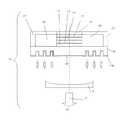
図6は、特許文献1や非特許文献1に開示された従来のVECSEL構造のレーザ装置の模式的断面図である。従来のレーザ装置90は、半導体基板40の上面に、n側多層膜反射鏡11、発光部13、及びp側多層膜反射鏡15を備え、発光部13を一対の反射鏡11及び15が半導体基板40の面に垂直な方向に挟み込む構成である。 FIG. 6 is a schematic cross-sectional view of a conventional laser device having a VECSEL structure disclosed in
また、p側多層膜反射鏡15の上層には、高濃度のコンタクト層17を介してp側電極21が形成されている。一方、発光部13や一対の反射鏡11及び15が形成されていない側において、半導体基板40の面上にはn側電極19が形成されている。 A p-
n側多層膜反射鏡11、発光部13、p側多層膜反射鏡15及びコンタクト層17の多層構造体の外側には絶縁層25が形成されている。この絶縁層25は、p側電極21とn側電極19の間にバイアス電圧が印加された際、発光効率を高めるべく発光部13を含む上記多層構造体の領域に電流を集中させ、その外側の領域に電流を流さないようにするための高抵抗層(電流狭窄層)を構成する。そして、この絶縁層25の周囲をパッシベーション層27が覆っている。 An
半導体基板40に対して、光取り出し方向d1の向きに離間した位置には、外部出力ミラー3が備えられている。 An
p側電極21とn側電極19の間にバイアス電圧を印加することにより、発光部13に電流が流れて当該領域が発光する。この光は、外部出力ミラー3、n側多層膜反射鏡11、及びp側多層膜反射鏡15によって形成される共振器で共振され、励起された光がレーザ光5として外部出力ミラー3から放出される。 By applying a bias voltage between the p-
なお、図6に示すレーザ装置90は、n側電極19の形成側がレーザ光5の取り出し面となっているため(取り出し方向d1)、n側電極19は、光の通路を遮らないような形状となっている。具体的には、図6のレーザ装置90においては、n側電極19がドーナツ形状を構成している。また、その内側の位置であって、半導体基板40のn側電極19が形成されている側の面上には、誘電体層29が形成されている。当該誘電体層29は、共振中の光の損失を抑制するために設けられている。 In the laser device 90 shown in FIG. 6, the formation side of the n-
コンタクト層17は、高濃度(例えば、1×10¹⁸/cm3以上)のキャリアがドープされており、p側電極21との間のコンタクト抵抗値を下げる役割を果たしている。The
ここで、同様に、n側電極19と半導体基板40の間の抵抗値を下げるべく、例えば半導体基板40を高濃度にドープする方法が考えられる。 Here, similarly, in order to lower the resistance value between the n-
しかし、一般的に高濃度にドープされた半導体層は、光を多く吸収することが知られている。図6の構成によれば、発光部13で生成された光は、外部出力ミラー3との間で半導体基板40内を通過しながら反射を繰り返した後、外部へと取り出される構成である。従って、半導体基板40を高濃度でドープした場合、発光部13で生成された光が半導体基板40内で吸収されてしまい、取り出し効率が低下するという問題がある。 However, it is generally known that highly doped semiconductor layers absorb a lot of light. According to the configuration of FIG. 6, the light generated by the
このような点に鑑み、特許文献1や非特許文献1の構成では、半導体基板40として、低濃度キャリア(例えば、5×10¹⁶/cm3以上、5×1017/cm3以下程度)のGaAs基板を採用している。In view of such points, in the configurations of
しかし、半導体基板40として、このような低濃度のGaAs基板を用いると、半導体基板40とn側電極19の間のコンタクト抵抗や、半導体基板40内の抵抗が大きくなる。このため、駆動時にp側電極21とn側電極19の間にバイアス電圧を印加すると高いジュール熱が発生し、これに起因してレーザ装置90が大きく昇温する。温度が上昇するとレーザ光5の波長が長波長側にシフトするため、所望の発光波長の光の取り出し効率は低下してしまう。 However, when such a low concentration GaAs substrate is used as the
なお、n側電極19と半導体基板40の間の抵抗値を下げるべく、n側電極19と半導体基板40の間に高濃度のコンタクト層を形成する方法も考えられる。しかし、この方法を採用した場合、n側電極19と半導体基板40の間のコンタクト抵抗値は低下させられるものの、低濃度の半導体基板40内を電流が通過することには変わりがないため、素子全体の抵抗を低下させることはできない。よって、高いジュール熱が発生してレーザ光5の波長が長波長側にシフトする点において、上記従来構成と同様の課題を有している。 A method of forming a high-concentration contact layer between the n-
本発明は、上記の点に鑑み、従来よりも光取り出し効率の高い半導体レーザ装置を提供することを目的とする。 In view of the above points, an object of the present invention is to provide a semiconductor laser device having higher light extraction efficiency than conventional ones.
本発明の半導体レーザ装置は、
半導体基板と、
前記半導体基板の第1面側の上層に形成された第1反射鏡と、
前記第1反射鏡の上層に形成された発光部と、
前記発光部の上層に形成された第2反射鏡と、
前記第2反射鏡の上層に形成されたコンタクト層と、
前記半導体基板の前記第1面と反対の第2面側の上層に形成された第1電極と、
前記コンタクト層の上層に形成された第2電極を備え、
前記第1電極は、前記半導体基板と接触し、当該半導体基板の発光部が形成されている半導体基板側に突き出た形状に形成され、この突き出た形状を複数個持つことを特徴とする。The semiconductor laser device of the present invention is
A semiconductor substrate;
A first reflecting mirror formed in an upper layer on the first surface side of the semiconductor substrate;
A light emitting part formed in an upper layer of the first reflecting mirror;
A second reflecting mirror formed on an upper layer of the light emitting unit;
A contact layer formed on an upper layer of the second reflecting mirror;
A first electrode formed in an upper layer on the second surface side opposite to the first surface of the semiconductor substrate;
A second electrode formed on the contact layer;
The first electrode is in contact with the semiconductor substrate and is formed in a shape protruding toward the semiconductor substrate on which the light emitting portion of the semiconductor substrate is formed, and has a plurality of protruding shapes.
上記構成によれば、半導体基板と第1電極間の電気を伝える接触面積は、半導体基板側に突き出た形状部の表面積分だけ加わり、増大する。つまり、半導体基板と第1電極間のコンタクト抵抗R(=(コンタクト抵抗率)X(長さ)÷(面積))は接触面積の増大に伴い低下し、ジュール熱を減らすことができる。
また、突き出た形状の電極部分を配置された部位は、半導体基板の厚さが薄くなるので、半導体基板内部の電気抵抗を減らせ、かつ、半導体基板自身の熱伝導率による温度上昇も減らすことができる。According to the above configuration, the contact area for transmitting electricity between the semiconductor substrate and the first electrode is increased by the surface integral of the shape portion protruding toward the semiconductor substrate. That is, the contact resistance R (= (contact resistivity) X (length) ÷ (area)) between the semiconductor substrate and the first electrode decreases with an increase in contact area, and Joule heat can be reduced.
In addition, since the thickness of the semiconductor substrate is reduced at the portion where the protruding electrode portion is disposed, the electrical resistance inside the semiconductor substrate can be reduced, and the temperature rise due to the thermal conductivity of the semiconductor substrate itself can be reduced. it can.
つまり、半導体基板と第1電極間オーミックコンタクトの電気抵抗率が大きくても、第1電極が半導体基板側へ突き出ることにより、これらの接触面積が増大する構成となる。よって、第1電極を半導体基板側に突き出た形状にすることで、第1電極から半導体基板までの電気抵抗を減らす構成にすることができる。従って、半導体基板から第1電極までに発生するジュール熱は、従来構成と比べて削減されるため、これに起因するレーザ装置の温度上昇が抑えられ、レーザ光の波長シフトも抑えられるため、所望の発光波長の光の取り出し効率が低下しない。 That is, even if the electrical resistivity of the ohmic contact between the semiconductor substrate and the first electrode is large, the contact area is increased by the first electrode protruding toward the semiconductor substrate. Therefore, by forming the first electrode in a shape protruding toward the semiconductor substrate, it is possible to reduce the electrical resistance from the first electrode to the semiconductor substrate. Therefore, since Joule heat generated from the semiconductor substrate to the first electrode is reduced as compared with the conventional configuration, the temperature rise of the laser device due to this is suppressed, and the wavelength shift of the laser light is also suppressed. The extraction efficiency of the light having the emission wavelength is not lowered.
また、第1電極は半導体基板側に突き出ているため、電気伝導路かつ熱伝導路でもある半導体基板の長さが短くでき、半導体基板内部の温度上昇は低い値が実現される。この結果、高いジュール熱が発生して、発光波長がシフトすることで、所望の発光波長の光の取り出し効率が低下するという問題も解消する。 Further, since the first electrode protrudes toward the semiconductor substrate, the length of the semiconductor substrate that is also an electric conduction path and a heat conduction path can be shortened, and a low value of temperature rise inside the semiconductor substrate is realized. As a result, high Joule heat is generated and the emission wavelength is shifted, so that the problem that the extraction efficiency of light having a desired emission wavelength is reduced is also solved.
つまり、上記の構成によれば、素子の低抵抗化と光の取り出し効率の向上という両者を同時に実現することができる That is, according to the above configuration, it is possible to simultaneously realize both the reduction of the resistance of the element and the improvement of the light extraction efficiency.
より具体的な第1の構成として、前記第1電極の半導体基板側に突き出た形状に円筒状を適用した構成とすることができる。 As a more specific first configuration, a cylindrical shape can be applied to the shape of the first electrode protruding toward the semiconductor substrate.
この構成では、円板部に側面の円筒部が追加された分だけ接触面積が増加している。
これにより、上記効果が実現される。In this configuration, the contact area is increased by the addition of the side cylindrical portion to the disc portion.
Thereby, the above effect is realized.
更にこのとき、円筒内部に第1電極材料を充填する構成としても構わない。 Further, at this time, the first electrode material may be filled inside the cylinder.
これらの構成によれば、半導体基板として低濃度キャリア基板を使用しても、第1電極から半導体基板までの電気抵抗を減らすことができる。よって、第1電極と半導体基板間のコンタクト抵抗を含む電気抵抗を減らし、ジュール熱による温度上昇を抑制することができ、安定して高い光の取り出し効率が実現される。 According to these configurations, even when a low-concentration carrier substrate is used as the semiconductor substrate, the electrical resistance from the first electrode to the semiconductor substrate can be reduced. Therefore, electrical resistance including contact resistance between the first electrode and the semiconductor substrate can be reduced, temperature rise due to Joule heat can be suppressed, and high light extraction efficiency can be realized stably.
また、より具体的な第2の構成として、前記第1電極の半導体基板側に突き出た形状が矩形溝の波板形状を適用した構成とすることができる。なお、本発明における波板形状とは、凹凸形状が平行して複数繰り返し形成されている状態を言う。 Further, as a more specific second configuration, a configuration in which the corrugated shape of a rectangular groove is applied to the shape of the first electrode protruding toward the semiconductor substrate side can be employed. In addition, the corrugated plate shape in the present invention refers to a state in which a plurality of uneven shapes are repeatedly formed in parallel.
この構成では、半導体基板側に突き出た矩形溝の側面部が追加された分だけ接触面積が増加している。また、第1電極は半導体基板側に突き出ているため、電気伝導路かつ熱伝導路でもある半導体基板の長さが短くなっている。これらにより上記効果が実現される。 In this configuration, the contact area is increased by the addition of the side surface portion of the rectangular groove protruding to the semiconductor substrate side. Further, since the first electrode protrudes toward the semiconductor substrate, the length of the semiconductor substrate that is also an electric conduction path and a heat conduction path is shortened. These effects are realized by these.
更にこのとき、第1電極の反半導体基板側(素子の外表面を形成する部分)の表面積(熱伝達面積)も増加するので、第1電極表面で発生する熱伝達による冷却効果も増大し、ますます、ジュール熱による温度上昇を抑制することができる。 In addition, since the surface area (heat transfer area) of the first electrode on the side opposite to the semiconductor substrate (the portion forming the outer surface of the element) is also increased, the cooling effect due to heat transfer generated on the surface of the first electrode is also increased. Increasingly, temperature rise due to Joule heat can be suppressed.
これらにより、素子の低抵抗化と光の取り出し効率の向上という両者を同時に実現することができる。 As a result, it is possible to simultaneously realize both a reduction in resistance of the element and an improvement in light extraction efficiency.
本発明の半導体レーザ装置によれば、光の通過経路上に高濃度領域を設けない状態で、コンタクト抵抗及び素子抵抗を低抵抗にすることができるので、従来よりも高い光取り出し効率が実現できる。 According to the semiconductor laser device of the present invention, since the contact resistance and the element resistance can be lowered without providing a high concentration region on the light passage path, higher light extraction efficiency can be realized than before. .
本発明の半導体レーザ装置(以下、適宜「レーザ装置」と略記する。)につき、図面を参照して説明する。なお、各図において図面の寸法比と実際の寸法比は必ずしも一致しない。 A semiconductor laser device of the present invention (hereinafter abbreviated as “laser device” as appropriate) will be described with reference to the drawings. In each figure, the dimensional ratio in the drawing does not necessarily match the actual dimensional ratio.
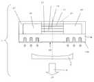
図1は、第1実施形態のレーザ装置の模式的断面図である。なお、図6と同一の要素に対しては、同一の符号を付している。 FIG. 1 is a schematic cross-sectional view of the laser apparatus of the first embodiment. In addition, the same code | symbol is attached | subjected to the element same as FIG.
(構成)
第1実施形態のレーザ装置1は、半導体基板10a、n側多層膜反射鏡11(「第1反射鏡」に対応)、発光部13、p側多層膜反射鏡15(「第2反射鏡」に対応)、コンタクト層17、n側電極19a(「第1電極」に対応)、p側電極21(「第2電極」に対応)を有する。(Constitution)
The
半導体基板10aの一方の面(「第1面」に対応)の上層にはn側多層膜反射鏡11が形成されており、n側多層膜反射鏡11の上層に発光部13が形成され、発光部13の上層にp側多層膜反射鏡15が形成される。p側多層膜反射鏡15の上層にコンタクト層17が形成され、コンタクト層17の上層にp側電極21が形成される。 The n-
また、半導体基板10aの他方の面(「第2面」に対応)には、n側電極19aが形成されている。 An n-
図1では、光取り出し方向d1は半導体基板10aの発光部13及び一対の反射鏡11,15が形成されている側と反対側であり、半導体基板10aとこの方向d1に離間した位置には外部出力ミラー3が形成される。なお、図6に示すレーザ装置90と同様に、図1に示すレーザ装置1も電流狭窄用の絶縁層25、パッシベーション層27、誘電体層29を備えている。 In FIG. 1, the light extraction direction d1 is opposite to the side where the
半導体基板10aは、例えばGaAs基板で構成される。ここで、本実施形態においては、半導体基板10aは、キャリア濃度が1×10¹⁸/cm3未満、より好ましくは5×1017/cm3以下の低濃度でドープされている。The
発光部13は、取り出すレーザ光5の波長に応じた材料で構成される。例えば、発光波長が0.8μm〜1μmの場合はGaInAs又はAlGaAsなどが用いられる。 The
n側多層膜反射鏡11及びp側多層膜反射鏡15は、所望の波長に対して吸収が少なく、且つ屈折率の異なる2種類の材料が積層されたもの、例えば、GaAs/AlGaAs又はGaAs/AlAsなどが用いられる。また、各反射鏡11,15を構成する各層の厚さは、材料及び波長に応じた厚さとされる。なお、p側多層膜反射鏡15の反射率を99%以上、n側多層膜反射鏡11の反射率を20%以上90%以下の範囲とするのが好ましい。n側多層膜反射鏡11の反射率をp側多層膜反射鏡15よりも低くしているのは、発光部13からの光が、n側多層膜反射鏡11とp側多層膜反射鏡15の間で反射を繰り返すことで励起された後、n側多層膜反射鏡11を通過して外部へと取り出す必要があるためである。 The n-
また、n側多層膜反射鏡11は、半導体基板10aと接触して形成されている。 The n-side multilayer
コンタクト層17は、p側多層膜反射鏡15の上層に形成される。コンタクト層17は、例えばGaAsで構成され、コンタクト抵抗を小さくするために炭素(C)などのp型不純物が1×10¹⁸/cm3以上の高濃度でドープされている。The
上述したように、n側電極19aは、半導体基板10aの発光部13及び一対の反射鏡11,15が形成されている側と反対側の面、すなわち光取り出し方向d1側の面に接触して形成されている。n側電極19aの材料としては、例えばNi/Ge/Au/Ni/AuやAu/Ge/Ni/Auなどが利用可能である。 As described above, the n-
p側電極21は、コンタクト層17の上層に形成される。p側電極21はn側電極19aと同一の材料で形成して構わない。 The p-
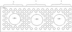
図2は、半導体基板10aを、光取り出し方向側すなわちn側電極19a側から見たときの模式的平面図である。なお、図2では、半導体基板10a上にレーザ装置1が複数配列されている状態(本実施例では3つ)を示しており、レーザ装置1からの光取り出し方向は紙面の手前側である。 FIG. 2 is a schematic plan view of the
このような構成の下、p側電極21とn側電極19aの間にバイアス電圧を印加すると、p側電極21、コンタクト層17、p側多層膜反射鏡15、発光部13、n側多層膜反射鏡11、半導体基板10a、及びn側電極19aからなる電流経路が形成される。これにより、発光部13に電流が流れ、当該領域が光を発する。この光は、p側多層膜反射鏡15、n側多層膜反射鏡11、及び外部出力ミラー3にて構成される共振器内を共振しながら励起され、レーザ光5として外部に取り出される。 Under such a configuration, when a bias voltage is applied between the p-
そして、n側電極19aは低いキャリア濃度の半導体基板10aに接触しているためコンタクト抵抗率は大きいが、n側電極19を半導体基板10側に突き出た形状にすることにより、n側電極19と半導体基板10との間の電気伝導面積を大きくし、且つ、コンタクト抵抗を小さくできる。また、半導体基板10a内部の電流経路長さを短くできるので半導体基板10内部の電圧降下も小さくできる。さらに、p側電極21は高濃度のコンタクト層17と接触しているので、コンタクト抵抗は低く抑えられる。これらにより素子全体の抵抗は低く抑えられる。これにより、高いジュール熱が発生して、発光波長がシフトし、所望の発光波長の光の取り出し効率が低下するという問題は解消する。 Since the n-
なお、図1の構成において、誘電体層29を備えない構成としても構わない。 In the configuration shown in FIG. 1, the
また、上記実施形態では、半導体基板10aの光取り出し方向d1側をn側、反対側をp側として説明したが、p側とn側の位置を反転させても構わない。以下の実施形態でも同様である。 Moreover, although the said embodiment demonstrated the light extraction direction d1 side of the
(製造方法)
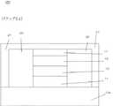
以下、図1に示すレーザ装置1の製造方法の一例につき、図3A〜図3Gの各工程断面図を参照して説明する。(Production method)
Hereinafter, an example of the manufacturing method of the
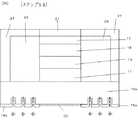
(ステップS1)
図3Aに示すように、半導体基板10a上に、n側多層膜反射鏡11、発光部13、p側多層膜反射鏡15及びコンタクト層17を下からこの順に結晶成長させる。(Step S1)
As shown in FIG. 3A, an n-
ここで、半導体基板10aとしては、例えばキャリア濃度が5×10¹⁷/cm3以下の低濃度のGaAs基板が採用される。Here, as the
n側多層膜反射鏡11としては、GaAs/AlGaAs又はGaAs/AlAsなどが用いられ、反射率が20%以上90%以下となるように積層数が設定される。発光部13としては、GaInAs又はAlGaAsなどが用いられ、発光波長に応じて採用される材料や組成比が設定される。p側多層膜反射鏡15としては、GaAs/AlGaAs又はGaAs/AlAsなどが用いられ、反射率が99%以上となるように積層数が設定される。なお、積層される膜厚の例としては、n側多層膜反射鏡11が100nm〜2000nm程度、発光部13が50nm〜2000nm程度、p側多層膜反射鏡15が1000nm〜5000nm程度である。 As the n-
また、コンタクト層17としては、例えばCなどのp型不純物が1×10¹⁸/cm3以上の高濃度でドープされたGaAsが膜厚10nm〜1000nm程度成膜される。As the
(ステップS2)
ステップS1で成膜された多層構造体を、ウェットエッチング法又はドライエッチング法によりメサ形状に加工する(図3B参照)。(Step S2)
The multilayer structure formed in step S1 is processed into a mesa shape by wet etching or dry etching (see FIG. 3B).
(ステップS3)
多層構造体のうち、例えば中央付近の領域をマスクしてイオン注入を行うことにより、電流狭窄層としての絶縁層25(高抵抗層)を形成する(図3C参照)。なお、当該箇所を酸化することで絶縁層25を形成してもよい。(Step S3)
Of the multilayer structure, for example, a region near the center is masked to perform ion implantation, thereby forming an insulating layer 25 (high resistance layer) as a current confinement layer (see FIG. 3C). Note that the insulating
(ステップS4)
図3Dに示すように、スパッタ法又はPVD(Physical Vapor Deposition:物理気相成長)法にて、例えばSiNやSiO2などの絶縁材料を膜厚10nm〜2000nm程度成膜し、パッシベーション層27を形成する。(Step S4)
As shown in FIG. 3D, an insulating material such as SiN or SiO2 is formed to a thickness of about 10 nm to 2000 nm by sputtering or PVD (Physical Vapor Deposition), and a
(ステップS5)
例えば、コンタクト層17の上方に係る位置以外をマスクして、ウェットエッチング法又はドライエッチング法により非マスク領域に形成されたパッシベーション層27を除去する。その後、当該領域にスパッタ法又は真空蒸着法によって例えばAu/Zn/AuやTi/Pt/Auなどの電極材料を膜厚100nm〜3000nm程度成膜して、p側電極21を形成する。(図3E参照)。(Step S5)
For example, the
(ステップS6)
その後、SiO2, Ta2O5, SiNOなどで構成される光学薄膜を、露出されている半導体基板10aの面に発光層13が形成されている側と反対側の方向から、スパッタ法又は真空蒸着法によって膜厚10nm〜1000nm程度成膜し、誘電体層29を形成する(図3F参照)(Step S6)
Thereafter, an optical thin film composed of SiO2 , Ta2 O5 , SiNO or the like is sputtered or vacuumed from the direction opposite to the side where the
(ステップS7)
半導体基板10aの発光層13が形成されている側と反対側の面に対し、ウェットエッチング法又はドライエッチング法により、基板面に直交する方向に半導体基板10a側にn側電極19aが突き出るように半導体基板10aに円筒状の凹みを形成する(図3G参照)。この凹みは、半導体基板10aの発光層13が形成されている側と反対側の面から見て環状(円環状など)を示す。(Step S7)
An n-
(ステップS8)
半導体基板10aの面に、発光層13が形成されている側と反対側の方向から、スパッタ法又は真空蒸着法によって例えばNi/Ge/Au/Ni/AuやAu/Ge/Ni/Auなどの電極材料を膜厚100nm〜3000nm程度成膜して、n側電極19を形成する(図3H参照)。(Step S8)
For example, Ni / Ge / Au / Ni / Au or Au / Ge / Ni / Au is formed on the surface of the
上記ステップS1〜S8を経てレーザ装置1を製造する方法は、あくまで一例であり、この方法に限定されるものではない。また、成膜する膜厚の条件や用いられる材料も一例であり、上述した内容に限定されるものではない。 The method of manufacturing the
レーザ装置の第2実施形態につき、第1実施形態と異なる箇所のみを説明する。 With respect to the second embodiment of the laser apparatus, only portions different from the first embodiment will be described.
(構成)
図4は、第2実施形態のレーザ装置の模式的断面図である。第2実施形態のレーザ装置1aにおいては、n側電極(第1電極)が半導体基板側に突き出た矩形溝の波板形状として形成されている。(Constitution)
FIG. 4 is a schematic cross-sectional view of the laser device of the second embodiment. In the
なお、本実施形態では、半導体基板10aは第1実施形態と同等のキャリア濃度、すなわち、例えばキャリア濃度が5×10¹⁷/cm3以下の低濃度のGaAs基板が採用される。In the present embodiment, the
図5は、図2にならって、本実施形態のレーザ装置1aが搭載された半導体基板10aを光取り出し方向側すなわちn側電極19a側から見たときの模式的平面図である。 FIG. 5 is a schematic plan view of the
このような構成においても、第1実施形態と同様、n側電極19aは低いキャリア濃度の半導体基板10aに接触しているためコンタクト抵抗率は大きい。しかし、n側電極19aを半導体基板10a側に突き出た形状にすることにより、n側電極19aと半導体基板10aとの間の電気伝導面積を大きくでき、且つ、コンタクト抵抗を小さくできる。
また、半導体基板10a内部の電流経路長さを短くできるので半導体基板10a内部の電圧降下も小さくできる。ここで、p側電極21は高濃度のコンタクト層17と接触しているので、コンタクト抵抗は低く抑えられている。さらに、n側電極19aの反半導体基板側の表面積(熱伝達面積)も増加するので、n側電極19a表面における熱伝達による冷却効果も増大する。これにより、ますます、ジュール熱による温度上昇を抑制することができる。
これらにより素子全体の抵抗は低く抑えられる。よって、高いジュール熱が発生して、発光波長がシフトすることで、所望の発光波長の光の取り出し効率が低下するという問題は解消できる。Even in such a configuration, since the n-
Further, since the current path length inside the
As a result, the resistance of the entire element can be kept low. Therefore, the problem that the extraction efficiency of light having a desired emission wavelength is reduced due to generation of high Joule heat and shift of the emission wavelength can be solved.
(製造方法)
図4に示すレーザ装置1aの製造方法については、第1実施形態と同じ手順で製造できるため、省略する。(Production method)
The manufacturing method of the
1 : 半導体レーザ装置
3 : 外部出力ミラー
5 : レーザ光
10 : 半導体基板
10a : 低キャリア濃度の半導体基板
11 : n側多層膜反射鏡(第1反射鏡)
13 : 発光部
15 : p側多層膜反射鏡(第2反射鏡)
17 : コンタクト層
19 : n側電極(第1電極)
19a : 非平面形状のn側電極(第1電極)
21 : p側電極(第2電極)
25 : 電流狭窄層としての絶縁層
27 : パッシベーション層
29 : 誘電体層
40 : 半導体基板
90 : 従来のVECSEL構造のレーザ装置
d1 : レーザ光の取り出し方向1: Semiconductor laser device 3: External output mirror 5: Laser light 10:
13: Light-emitting part 15: P-side multilayer reflector (second reflector)
17: contact layer 19: n-side electrode (first electrode)
19a: Non-planar n-side electrode (first electrode)
21: p-side electrode (second electrode)
25: Insulating layer as a current confinement layer 27: Passivation layer 29: Dielectric layer 40: Semiconductor substrate 90: Conventional laser device with VECSEL structure d1: Laser beam extraction direction
Claims (4)
Translated fromJapanese前記半導体基板の第1面側の上層に形成された第1反射鏡と、
前記第1反射鏡の上層に形成された発光部と、
前記発光部の上層に形成された第2反射鏡と、
前記第2反射鏡の上層に形成されたコンタクト層と、
前記半導体基板の前記第1面と反対の第2面側の上層に形成された第1電極と、
前記コンタクト層の上層に形成された第2電極と、を備え、
前記第1電極は、前記半導体基板と接触し、当該半導体基板の発光部が形成されている半導体基板側に突き出た形状に形成され、この突き出た形状を複数個持つことを特徴とする半導体レーザ装置。A semiconductor substrate;
A first reflecting mirror formed in an upper layer on the first surface side of the semiconductor substrate;
A light emitting part formed in an upper layer of the first reflecting mirror;
A second reflecting mirror formed on an upper layer of the light emitting unit;
A contact layer formed on an upper layer of the second reflecting mirror;
A first electrode formed in an upper layer on the second surface side opposite to the first surface of the semiconductor substrate;
A second electrode formed on an upper layer of the contact layer,
The first electrode is in contact with the semiconductor substrate and is formed in a shape protruding toward the semiconductor substrate on which the light emitting portion of the semiconductor substrate is formed, and has a plurality of protruding shapes apparatus.
Priority Applications (1)
| Application Number | Priority Date | Filing Date | Title |
|---|---|---|---|
| JP2013057801AJP2014183251A (en) | 2013-03-21 | 2013-03-21 | Semiconductor laser device |
Applications Claiming Priority (1)
| Application Number | Priority Date | Filing Date | Title |
|---|---|---|---|
| JP2013057801AJP2014183251A (en) | 2013-03-21 | 2013-03-21 | Semiconductor laser device |
Publications (1)
| Publication Number | Publication Date |
|---|---|
| JP2014183251Atrue JP2014183251A (en) | 2014-09-29 |
Family
ID=51701655
Family Applications (1)
| Application Number | Title | Priority Date | Filing Date |
|---|---|---|---|
| JP2013057801APendingJP2014183251A (en) | 2013-03-21 | 2013-03-21 | Semiconductor laser device |
Country Status (1)
| Country | Link |
|---|---|
| JP (1) | JP2014183251A (en) |
Cited By (1)
| Publication number | Priority date | Publication date | Assignee | Title |
|---|---|---|---|---|
| CN112134138A (en)* | 2020-08-18 | 2020-12-25 | 华芯半导体科技有限公司 | High-power vcsel chip and preparation method thereof |
- 2013
- 2013-03-21JPJP2013057801Apatent/JP2014183251A/enactivePending
Cited By (1)
| Publication number | Priority date | Publication date | Assignee | Title |
|---|---|---|---|---|
| CN112134138A (en)* | 2020-08-18 | 2020-12-25 | 华芯半导体科技有限公司 | High-power vcsel chip and preparation method thereof |
Similar Documents
| Publication | Publication Date | Title |
|---|---|---|
| JP4548345B2 (en) | Surface emitting semiconductor laser | |
| JP2015041688A (en) | Semiconductor laser device | |
| US10033158B1 (en) | Semiconductor laser, laser assembly and method of making a semiconductor laser | |
| CA2302103C (en) | Quantum well type light-emitting diode | |
| JP2019208004A (en) | Vertical resonator type light-emitting device | |
| US8218596B2 (en) | Vertical cavity surface emitting laser and method of manufacturing the same | |
| JP7570351B2 (en) | Surface-emitting laser, surface-emitting laser array, electronic device, and method for manufacturing surface-emitting laser | |
| JP6098820B2 (en) | Semiconductor laser device | |
| JP4605024B2 (en) | Surface emitting semiconductor laser | |
| JP2017216285A (en) | Surface emitting laser array device, light source unit, and laser device | |
| JP2017084847A (en) | Vertical resonator light-emitting element and method of manufacturing the same | |
| JP4592873B2 (en) | Surface emitting semiconductor laser device | |
| JP3785683B2 (en) | Surface light emitting device | |
| JP2014183251A (en) | Semiconductor laser device | |
| JP4548329B2 (en) | Surface emitting semiconductor laser | |
| JP2018073931A (en) | Surface emission laser element and atomic oscillator | |
| JP2017204616A (en) | Surface emitting laser element, atomic oscillator | |
| JP6828272B2 (en) | Surface emitting laser, surface emitting laser array, light source unit and laser device | |
| WO2019107273A1 (en) | Surface emission semiconductor laser | |
| JP2008251719A (en) | Surface emitting laser element and method for manufacturing surface emitting laser element | |
| JP2005251860A (en) | Surface emitting laser device | |
| CN115693392A (en) | Vertical cavity surface emitting laser and manufacturing method thereof | |
| JP2008244240A (en) | Surface emitting semiconductor laser, method for manufacturing the same, and optical module | |
| JP5261201B2 (en) | Surface emitting laser, surface emitting laser array and manufacturing method thereof | |
| JP2014170813A (en) | Semiconductor laser device |