JP2014170773A - Multilayer coil and manufacturing method thereof - Google Patents
Multilayer coil and manufacturing method thereofDownload PDFInfo
- Publication number
- JP2014170773A JP2014170773AJP2013040467AJP2013040467AJP2014170773AJP 2014170773 AJP2014170773 AJP 2014170773AJP 2013040467 AJP2013040467 AJP 2013040467AJP 2013040467 AJP2013040467 AJP 2013040467AJP 2014170773 AJP2014170773 AJP 2014170773A
- Authority
- JP
- Japan
- Prior art keywords
- coil
- insulator layer
- layer
- conductor
- laminated
- Prior art date
- Legal status (The legal status is an assumption and is not a legal conclusion. Google has not performed a legal analysis and makes no representation as to the accuracy of the status listed.)
- Granted
Links
- 238000004519manufacturing processMethods0.000titleclaimsabstractdescription30
- 239000004020conductorSubstances0.000claimsabstractdescription157
- 239000012212insulatorSubstances0.000claimsabstractdescription143
- 238000003475laminationMethods0.000claimsabstractdescription25
- 238000000034methodMethods0.000claimsdescription20
- 239000000463materialSubstances0.000claimsdescription18
- 239000000696magnetic materialSubstances0.000claimsdescription8
- 238000010030laminatingMethods0.000claims1
- 230000003247decreasing effectEffects0.000abstract1
- 239000000919ceramicSubstances0.000description15
- 230000000740bleeding effectEffects0.000description7
- 238000003780insertionMethods0.000description5
- 230000037431insertionEffects0.000description5
- 229910052709silverInorganic materials0.000description5
- 239000011230binding agentSubstances0.000description3
- 230000015572biosynthetic processEffects0.000description3
- 239000005388borosilicate glassSubstances0.000description3
- 229910052802copperInorganic materials0.000description3
- 230000007547defectEffects0.000description3
- 239000000945fillerSubstances0.000description3
- 238000012986modificationMethods0.000description3
- 230000004048modificationEffects0.000description3
- 229910052763palladiumInorganic materials0.000description3
- 230000000149penetrating effectEffects0.000description3
- BQCADISMDOOEFD-UHFFFAOYSA-NSilverChemical compound[Ag]BQCADISMDOOEFD-UHFFFAOYSA-N0.000description2
- 238000001035dryingMethods0.000description2
- 239000002003electrode pasteSubstances0.000description2
- 238000010304firingMethods0.000description2
- 229910052759nickelInorganic materials0.000description2
- 238000007747platingMethods0.000description2
- 239000004332silverSubstances0.000description2
- 239000000758substrateSubstances0.000description2
- 229910000859α-FeInorganic materials0.000description2
- PNEYBMLMFCGWSK-UHFFFAOYSA-Naluminium oxideInorganic materials[O-2].[O-2].[O-2].[Al+3].[Al+3]PNEYBMLMFCGWSK-UHFFFAOYSA-N0.000description1
- QVGXLLKOCUKJST-UHFFFAOYSA-Natomic oxygenChemical compound[O]QVGXLLKOCUKJST-UHFFFAOYSA-N0.000description1
- 238000010586diagramMethods0.000description1
- 230000000694effectsEffects0.000description1
- 229910052760oxygenInorganic materials0.000description1
- 239000001301oxygenSubstances0.000description1
- 230000035699permeabilityEffects0.000description1
- 239000000843powderSubstances0.000description1
- 238000004904shorteningMethods0.000description1
- 239000000126substanceSubstances0.000description1
- 238000004804windingMethods0.000description1
Images


Classifications
- H—ELECTRICITY
- H01—ELECTRIC ELEMENTS
- H01F—MAGNETS; INDUCTANCES; TRANSFORMERS; SELECTION OF MATERIALS FOR THEIR MAGNETIC PROPERTIES
- H01F5/00—Coils
- H01F5/003—Printed circuit coils
- H—ELECTRICITY
- H01—ELECTRIC ELEMENTS
- H01F—MAGNETS; INDUCTANCES; TRANSFORMERS; SELECTION OF MATERIALS FOR THEIR MAGNETIC PROPERTIES
- H01F41/00—Apparatus or processes specially adapted for manufacturing or assembling magnets, inductances or transformers; Apparatus or processes specially adapted for manufacturing materials characterised by their magnetic properties
- H01F41/02—Apparatus or processes specially adapted for manufacturing or assembling magnets, inductances or transformers; Apparatus or processes specially adapted for manufacturing materials characterised by their magnetic properties for manufacturing cores, coils, or magnets
- H01F41/04—Apparatus or processes specially adapted for manufacturing or assembling magnets, inductances or transformers; Apparatus or processes specially adapted for manufacturing materials characterised by their magnetic properties for manufacturing cores, coils, or magnets for manufacturing coils
- H01F41/041—Printed circuit coils
- H01F41/046—Printed circuit coils structurally combined with ferromagnetic material
Landscapes
- Engineering & Computer Science (AREA)
- Power Engineering (AREA)
- Manufacturing & Machinery (AREA)
- Coils Or Transformers For Communication (AREA)
- Manufacturing Cores, Coils, And Magnets (AREA)
Abstract
Description
Translated fromJapanese本発明は、積層コイル及びその製造方法に関する。 The present invention relates to a laminated coil and a manufacturing method thereof.
従来の積層コイルとしては、例えば、特許文献1に記載の積層電子部品が知られている。図28は、特許文献1に記載の積層電子部品500の分解斜視図である。図29は、特許文献1に記載の積層電子部品500のセラミックグリーンシート501h及びコイル形成導体502gの平面図である。以下で、セラミックグリーンシートの積層方向をz軸方向とし、z軸方向の正方向側の面を上面、負方向側の面を下面と称す。また、セラミックグリーンシートの長辺方向をx軸方向とし、短辺方向をy軸方向とする。なお、x軸、y軸及びz軸は、互いに直交している。 As a conventional multilayer coil, for example, a multilayer electronic component described in
積層電子部品500は、図28に示すように、セラミックグリーンシート501a〜501j、コイル形成導体502a〜502h、ビアホール導体503a〜503g及び端子電極(図示せず)により構成されている。なお、セラミックグリーンシート501a〜501jは、z軸方向から平面視したときに、長方形状を成す絶縁体層である。また、コイル形成導体502a〜502gは、z軸方向から平面視したときに、環状の長方形の一部が切り欠かれた形状を成す線状の導体層である。また、コイル形成導体502hは、セラミックグリーンシート501iの上面に設けられた導体層である。 As shown in FIG. 28, the multilayer
積層電子部品500では、セラミックグリーンシート501iの上面にコイル形成導体502hが設けられ、コイル形成導体502hの上面にセラミックグリーンシート501hが設けられるというように、セラミックグリーンシート501a〜501iとコイル形成導体502a〜502hとが交互に積層されている。ただし、セラミックグリーンシート501iは、セラミックグリーンシート501jの上面に積層されている。また、コイル形成導体502a〜502hは、ビアホール導体503a〜503gにより接続されている。なお、コイル形成導体502a,502hは、積層電子部品500の側面に設けられた端子電極とも接続されている。 In the multilayer
ところで、積層電子部品500では、コイル形成導体502gを印刷する際の滲みや印刷ずれによるショート不良を防止するために、図29に示すように、コイル形成導体502gの端部であるパッド部504,505の間隔d500を大きくしている。具体的には、パッド部504からパッド部505をx軸方向およびy軸方向の正方向側に遠ざけている。しかし、パッド部504,505の間隔を大きくした分だけ、コイル形成導体502gの長さが短くなっている。同様に、コイル形成導体502a〜502fにおいても、パッド部の間隔を大きくしているため、コイル形成導体502a〜502fの長さがそれぞれ短くなっている。結果として、積層電子部品500では、コイル形成導体502a〜502gからなるコイルの巻き数が減少し、コイルとしての所望の特性を得ることが困難であった。 By the way, in the multilayer
そこで、本発明の目的は、コイルの巻き数を減少させることなく、当該コイル導体の印刷時の滲み等によるショート不良を抑制することができる積層コイル及びその製造方法を提供することである。 Accordingly, an object of the present invention is to provide a laminated coil and a method for manufacturing the same that can suppress short-circuit failure due to bleeding or the like during printing of the coil conductor without reducing the number of turns of the coil.
本発明の一形態に係る積層コイルは、所定の絶縁体層を含む複数の絶縁体層が積層されてなる積層体と、前記所定の絶縁体層上において周回している線状のコイル導体と、前記所定の絶縁体層上に設けられ、かつ、前記コイル導体において互いに最も近接している第1の部分と第2の部分とに挟まれる差挟み部と、を備え、前記第1の部分は、該第1の部分と前記差挟み部との界面において、該差挟み部より積層方向上側に位置すること、を特徴とする。 A laminated coil according to an aspect of the present invention includes a laminated body in which a plurality of insulating layers including a predetermined insulating layer are stacked, and a linear coil conductor that circulates on the predetermined insulating layer. A first sandwiching portion provided on the predetermined insulator layer, and sandwiched between a first portion and a second portion that are closest to each other in the coil conductor, and the first portion Is characterized in that it is located on the upper side in the stacking direction from the difference sandwiching portion at the interface between the first portion and the difference sandwiching portion.
本発明の一形態に係る積層コイルの製造方法は、所定の絶縁体層を含む複数の絶縁体層が積層されてなる積層体、該所定の絶縁体層上において周回している線状のコイル導体、及び該所定の絶縁体層上に設けられ、かつ、該コイル導体において互いに最も近接している第1の部分と第2の部分とに挟まれる差挟み部を含む積層コイルの製造方法であって、前記所定の絶縁体層を形成する工程と、前記所定の絶縁体層上に前記差挟み部を形成する工程と、前記差挟み部が形成された前記所定の絶縁体層上に前記コイル導体を形成する工程と、を備えること、を特徴とする。 A method for manufacturing a laminated coil according to an aspect of the present invention includes a laminate in which a plurality of insulator layers including a prescribed insulator layer are laminated, and a linear coil that circulates on the prescribed insulator layer. A method of manufacturing a laminated coil including a conductor and a differential sandwiching portion provided on the predetermined insulator layer and sandwiched between a first portion and a second portion that are closest to each other in the coil conductor. A step of forming the predetermined insulator layer; a step of forming the differential sandwich portion on the predetermined insulator layer; and the step of forming the differential insulator portion on the predetermined insulator layer in which the differential sandwich portion is formed. And a step of forming a coil conductor.
本発明に係る積層コイル及びその製造方法によれば、一の絶縁体層上に形成されたコイル導体の長さを短くすることなく、当該コイル導体の印刷時の滲み等によるショート不良を抑制することができる。 According to the laminated coil and the method of manufacturing the same according to the present invention, short-circuit failure due to bleeding or the like during printing of the coil conductor is suppressed without shortening the length of the coil conductor formed on one insulator layer. be able to.
以下に、本発明の一形態に係る積層コイル及びその製造方法について説明する。 Hereinafter, a laminated coil and a manufacturing method thereof according to an embodiment of the present invention will be described.
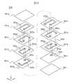
以下に、本発明の一形態に係る積層コイル10の構成について図面を参照しながら説明する。図1は、本発明の一形態に係る積層コイル10の外観斜視図である。図2は、本発明の一形態に係る積層コイル10の積層体20の分解斜視図である。図3,5,7は、本発明の一形態に係る積層コイル10の絶縁体層22b,22d,22f、コイル導体40a〜40c及び差挟み部50a〜50cを積層方向から平面視した図である。図4は、図3のA−A断面における断面図である。図6は、図5のB−B断面における断面図である。図8は、図7のC−C断面における断面図である。以下、積層コイル10の積層方向をz軸方向と定義し、z軸方向から平面視したときに、積層コイル10の各辺に沿った方向をx軸方向及びy軸方向と定義する。なお、x軸、y軸及びz軸は互いに直交している。 Below, the structure of the laminated
(積層コイルの概略構成)
積層コイル10は、積層体20、外部電極30a,30b、コイル導体40a〜40c、ビアホール導体42a〜42c及び差挟み部50a〜50cを備えている。また、積層コイル10は、図1に示すように、直方体である。(Schematic configuration of laminated coil)
The
(積層体の構成)
積層体20は、図2に示すように、絶縁体層22a〜22iがz軸方向の正方向側からこの順に並ぶように積層されることにより構成されている。また、各絶縁体層22a〜22iは、z軸方向から平面視したときに、長方形状を成している。従って、絶縁体層22a〜22iが積層されることにより構成された積層体20は、図1に示すように、直方体である。なお、各絶縁体層22a〜22iのz軸方向の正方向側の面を上面と称し、各絶縁体層22a〜22iのz軸方向の負方向側の面を下面と称す。(Structure of laminate)
As illustrated in FIG. 2, the
絶縁体層22aは、図2に示すように、積層体20のz軸方向の正方向側の端部に位置する。また、絶縁体層22aは、磁性体層24aにより構成されている。なお、磁性体層24a及び後述する磁性体層24b〜24iの材料は、フェライト等の磁性体である。 As shown in FIG. 2, the insulator layer 22 a is located at the end of the stacked
絶縁体層22bは、図2に示すように、絶縁体層22aの下面側に位置する。また、絶縁体層22bは、磁性体層24bにより構成されている。さらに、絶縁体層22bの外縁を構成するx軸方向の正方向側の辺と絶縁体層22bの外縁を構成するy軸方向の正方向側の辺とが成す角の近傍には、絶縁体層22bをz軸方向に貫通する矩形状の貫通孔60aが設けられている。なお、絶縁体層22bの内部に、後述するコイル導体40aが位置している。 As shown in FIG. 2, the
絶縁体層22c(所定の絶縁体層)は、図2に示すように、絶縁体層22bの下面側に位置する。また、絶縁体層22cは、磁性体層24c及び非磁性体層26aにより構成されている。非磁性体層26aは、絶縁体層22cの外縁と平行に設けられた帯状の非磁性体層であり、z軸方向から平面視したときに、略ロの字型の形状を成している。また、磁性体層24cは、z軸方向から平面視したときに、非磁性体層26aの周囲、及び非磁性体層26aのロの字の内部に設けられている。なお、非磁性体層26a及び後述する非磁性体層26b〜26cの材料は、硼珪酸ガラス及びセラミックスフィラー等の非磁性体である。 The
絶縁体層22dは、図2に示すように、絶縁体層22cの下面側に位置する。また、絶縁体層22dは、磁性体層24dにより構成されている。さらに、絶縁体層22dの外縁を構成するx軸方向の正方向側の辺と絶縁体層22dの外縁を構成するy軸方向の正方向側の辺とが成す角の近傍には、絶縁体層22dをz軸方向に貫通する矩形状の貫通孔60bが設けられている。なお、絶縁体層22dの内部に、後述するコイル導体40bが位置している。 As shown in FIG. 2, the
絶縁体層22e(所定の絶縁体層)は、図2に示すように、絶縁体層22dの下面側に位置する。また、絶縁体層22eは、磁性体層24e及び非磁性体層26bにより構成されている。非磁性体層26bは、絶縁体層22eの外縁と平行に設けられた帯状の非磁性体層であり、z軸方向から平面視したときに、略ロの字型の形状を成している。また、磁性体層24eは、z軸方向から平面視したときに、非磁性体層26bの周囲、及び非磁性体層26bのロの字の内部に設けられている。 The
絶縁体層22fは、図2に示すように、絶縁体層22eの下面側に位置する。また、絶縁体層22fは、磁性体層24fにより構成されている。さらに、絶縁体層22fの外縁を構成するx軸方向の正方向側の辺と絶縁体層22fの外縁を構成するy軸方向の正方向側の辺とが成す角の近傍には、絶縁体層22fをz軸方向に貫通する矩形状の貫通孔60cが設けられている。なお、絶縁体層22fの内部に、後述するコイル導体40cが位置している。 As shown in FIG. 2, the
絶縁体層22g(所定の絶縁体層)は、図2に示すように、絶縁体層22fの下面側に位置する。また、絶縁体層22gは、磁性体層24g及び非磁性体層26cにより構成されている。非磁性体層26cは、絶縁体層22gの外縁と平行に設けられた帯状の非磁性体層であり、z軸方向から平面視したときに、略ロの字型の形状を成している。また、磁性体層24gは、z軸方向から平面視したときに、非磁性体層26cの周囲、及び非磁性体層26cのロの字の内部に設けられている。 As shown in FIG. 2, the
絶縁体層22hは、図2に示すように、絶縁体層22gの下面側に位置する。また、絶縁体層22hは、磁性体層24hにより構成されている。なお、絶縁体層22hの内部に、後述するコイル導体40dが設けられている。 As shown in FIG. 2, the
絶縁体層22iは、図2に示すように、絶縁体層22hの下面側に位置している。また、絶縁体層22iは、積層体20のz軸方向の負方向側の端部に位置している。絶縁体層22iは、磁性体層24iにより構成されている。 As shown in FIG. 2, the insulator layer 22i is located on the lower surface side of the
(外部電極の構成)
外部電極30aは、図1に示すように、積層体20のx軸方向の正方向側の側面S1を覆うように設けられている。外部電極30bは、積層体20のx軸方向の負方向側の側面S2を覆うように設けられている。また、外部電極30a,30bの材料は、Ag,Pd,Cu,Ni等の導電性材料である。(External electrode configuration)
As shown in FIG. 1, the external electrode 30 a is provided so as to cover the side surface S <b> 1 on the positive side in the x-axis direction of the
(コイル導体の構成)
コイル導体40aは、図2に示すように、絶縁体層22b内に埋め込まれており、絶縁体層22bと同じ厚さを有している。よって、コイル導体40aは、絶縁体層22bの下面側に露出している。つまり、コイル導体40aは、絶縁体層22c(所定の絶縁体層)の上面側に設けられている。なお、コイル導体40aは、コイル本体部41aと引き出し部43aに分けられる。(Configuration of coil conductor)
As shown in FIG. 2, the
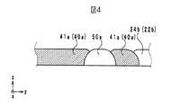
コイル本体部41aは、絶縁体層22bの外縁と平行に設けられた帯状の導体層である。これにより、コイル本体部41aは、z軸方向から平面視したときに、略ロの字型の形状を成して、絶縁体層22cの上面側を周回している。よって、コイル本体部41aは、螺旋状のコイルの略1周分の長さを有している。ただし、コイル本体部41aは、貫通孔60aが位置する箇所で分断されている。すなわち、コイル本体部41aの両端部は、貫通孔60aが位置する箇所で最も近接している。 The coil
引き出し部43aは、コイル導体40aの一端(第1の部分)と積層体20の側面S1に位置する外部電極30aとを接続している。コイル導体40aの他端(第2の部分)は、絶縁体層22cをz軸方向に貫通するビアホール導体42aと接続されている。以上より、コイル導体40aは、z軸方向の正方向側から見たときに、外部電極30aからビアホール導体42aまでを、時計回りに周回しながら接続している。なお、コイル導体40a、後述するコイル導体40b〜40d及びビアホール導体42a及び後述するビアホール導体42b〜42cそれぞれの材料は、Ag,Pd,Cu,Ni等の導電性材料である。 The
コイル導体40bは、図2に示すように、絶縁体層22d内に埋め込まれており、絶縁体層22dと同じ厚さを有している。よって、コイル導体40bは、絶縁体層22dの下面側に露出している。つまり、コイル導体40bは、絶縁体層22e(所定の絶縁体層)の上面側に設けられている。また、コイル導体40bは、絶縁体層22dの外縁と平行に設けられた帯状の導体層である。これにより、コイル導体40bは、z軸方向から平面視したときに、略ロの字型の形状を成して、絶縁体層22eの上面側を周回している。よって、コイル導体40bは、螺旋状のコイルの略1周分の長さを有している。ただし、コイル導体40bは、貫通孔60bが位置する箇所で分断されている。すなわち、コイル導体40bの両端部は、貫通孔60bが位置する箇所で最も近接している。ここで、コイル導体40bの一端(第1の部分)は、ビアホール導体42aと接続されている。これにより、コイル導体40bは、コイル導体40aと電気的に接続されている。なお、コイル導体40a,40bは、非磁性体層26aを挟んで対向している。コイル導体40bの他端(第2の部分)は、絶縁体層22eをz軸方向に貫通するビアホール導体42bと接続されている。以上より、コイル導体40bは、z軸方向の正方向側から見たときに、ビアホール導体42aからビアホール導体42bまでを、時計回りに周回しながら接続している。 As shown in FIG. 2, the
コイル導体40cは、図2に示すように、絶縁体層22f内に埋め込まれており、絶縁体層22fと同じ厚さを有している。よって、コイル導体40cは、絶縁体層22fの下面側に露出している。つまり、コイル導体40cは、絶縁体層22g(所定の絶縁体層)の上面側に設けられている。また、コイル導体40cは、絶縁体層22fの外縁と平行に設けられた帯状の導体層である。これにより、コイル導体40cは、z軸方向から平面視したときに、略ロの字型の形状を成して、絶縁体層22gの上面側を周回している。よって、コイル導体40cは、螺旋状のコイルの略1周分の長さを有している。ただし、コイル導体40cは、貫通孔60cが位置する箇所で分断されている。すなわち、コイル導体40cの両端部は、貫通孔60cが位置する箇所で最も近接している。ここで、コイル導体40cの一端(第1の部分)は、ビアホール導体42bと接続されている。これにより、コイル導体40cは、コイル導体40bと電気的に接続されている。なお、コイル導体40b,40cは、非磁性体層26bを挟んで対向している。コイル導体40cの他端(第2の部分)は、絶縁体層22gをz軸方向に貫通するビアホール導体42cと接続されている。以上より、コイル導体40cは、z軸方向の正方向側から見たときに、ビアホール導体42bからビアホール導体42cまでを、時計回りに周回しながら接続している。 As shown in FIG. 2, the
コイル導体40dは、図2に示すように、絶縁体層22h内に埋め込まれており、絶縁体層22hと同じ厚さを有している。よって、コイル導体40dは、絶縁体層22hの下面側に露出している。つまり、コイル導体40dは、絶縁体層22iの上面側に設けられている。また、コイル導体40dは、絶縁体層22hの外縁を成すx軸方向の正負両方向側の辺及びy軸方向の負方向側の辺と平行に設けられた帯状の導体層である。ただし、コイル導体40dにおけるx軸方向の負方向側と平行な部分は、y軸方向の中央付近で積層体20の側面S2に引き出されている。従って、コイル導体40dの一端は、外部電極30bと接続されている。また、コイル導体40dの他端は、ビアホール導体42cと接続されている。これにより、コイル導体40dは、コイル導体40cと電気的に接続されている。なお、コイル導体40c,40dは、非磁性体層26cを挟んで対向している。 As shown in FIG. 2, the
(差挟み部の構成)
差挟み部50aは、図2に示すように、絶縁体層22cの上面側に設けられている。また、差挟み部50aは、z軸方向から見たとき、貫通孔60aと重なる位置に設けられている。これにより、絶縁体層22bと絶縁体層22cとが、積層された際には、図3及び図4に示すように、コイル本体部41aの両端部(第1の部分と第2の部分)に挟まれている。なお、差挟み部50a及び後述する差挟み部50b、50cの材料は、硼珪酸ガラス及びセラミックスフィラー等の非磁性体である。(Structure of the sandwiching part)
As shown in FIG. 2, the
差挟み部50bは、図2に示すように、絶縁体層22eの上面側に設けられている。また、差挟み部50bは、z軸方向から見たとき、貫通孔60bと重なる位置に設けられている。これにより、絶縁体層22dと絶縁体層22eとが、積層された際には、図5及び図6に示すように、コイル導体40bの両端部(第1の部分と第2の部分)に挟まれている。 As shown in FIG. 2, the
差挟み部50cは、図2に示すように、絶縁体層22gの上面側に設けられている。また、差挟み部50cは、z軸方向から見たとき、貫通孔60cと重なる位置に設けられている。これにより、絶縁体層22fと絶縁体層22gとが、積層された際には、図7及び図8に示すように、コイル導体40cの両端部(第1の部分と第2の部分)に挟まれている。 As shown in FIG. 2, the
(積層コイルの製造方法)
積層コイル10の製造方法について図面を参照しながら説明する。なお、図9乃至図24では、一つの積層コイル10が作成される工程を図示しているが、実際には、積層コイル10の集合体であるマザー積層体が同時に作製される。図9,11,13,15,17,19,21,23は、製造途中の積層コイル10をz軸方向の正方向側から平面視した図である。図10は、図9のD−D断面における断面図である。図12は、図11のE−E断面における断面図である。図14は、図13のF−F断面における断面図である。図16は、図15のG−G断面における断面図である。図18は、図17のH−H断面における断面図である。図20は、図19のI−I断面における断面図である。図22は、図21のJ−J断面における断面図である。図24は、図23のK−K断面における断面図である。(Manufacturing method of laminated coil)
A method for manufacturing the
まず、図9及び図10に示すように、磁性体材料であるフェライト粉末をバインダー等の有機成分と混合してペースト状にした磁性体ペーストを、印刷工法によりアルミナ基板(図示しない)等の保持基板上に塗布し、乾燥させて絶縁体層22iを形成する。 First, as shown in FIGS. 9 and 10, a magnetic paste obtained by mixing ferrite powder, which is a magnetic material, with an organic component such as a binder to form a paste is held on an alumina substrate (not shown) by a printing method. The insulating layer 22i is formed by applying on a substrate and drying.
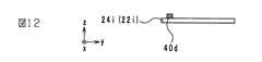
次に、図11及び図12に示すように、Ag,Pd,Cu,Ni等を主成分とする導電性ペーストを、印刷工法により絶縁体層22i上に塗布し、乾燥させてコイル導体40dを形成する。さらに、図13及び図14に示すように、磁性体ペーストを、印刷工法により絶縁体層22i上のコイル導体40dが形成されていない部分に塗布し、乾燥させて磁性体層24h(絶縁体層22h)を形成する。 Next, as shown in FIGS. 11 and 12, a conductive paste mainly composed of Ag, Pd, Cu, Ni or the like is applied onto the insulator layer 22i by a printing method and dried to form the
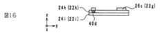
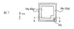
次に、図15及び図16に示すように、硼珪酸ガラス及びセラミックフィラーにより構成された非磁性体ペーストを、コイル導体40dを覆うように、印刷工法により絶縁体層22h及びコイル導体40d上に塗布し、乾燥させて非磁性体層26cを形成する。さらに、図17及び図18に示すように、磁性体ペーストを、印刷工法により絶縁体層22h上の非磁性体層26cが形成されていない部分に塗布し、乾燥させて磁性体層24gを形成する。結果として、絶縁体層22gが形成される。なお、絶縁体層22gを形成する際に、ビアホール導体42cを形成するためのビアホールを設けておく。そして、絶縁体層22gの形成後に、印刷工法により導電性ペーストをビアホールに充填し、ビアホール導体42cを形成する。 Next, as shown in FIGS. 15 and 16, a non-magnetic paste composed of borosilicate glass and ceramic filler is applied onto the
次に、図19及び図20に示すように、非磁性体ペーストを、印刷工法により非磁性体層26cの上面に塗布し、乾燥させて差挟み部50cを形成する。非磁性体ペーストを塗布する箇所は、z軸方向から見て、差挟み部50cを形成した後に形成されるコイル導体40cの両端(第1の部分及び第2の部分)に挟まれた箇所である。 Next, as shown in FIGS. 19 and 20, a non-magnetic paste is applied to the upper surface of the
次に、図21及び図22に示すように、導電性ペーストを、印刷工法により絶縁体層22gの非磁性体層26c上に塗布し、乾燥させてコイル導体40cを形成する。このとき、コイル導体40cの両端(第1の部分および第2の部分)は、差挟み部50cにより隔てられている。なお、導電性ペーストは、差挟み部50cの形成後に塗布される。従って、コイル導体40cは、図8に示すように、差挟み部50cとの界面において、差挟み部50cよりもz軸方向の正方向側に位置する。より詳細には、コイル導体40cと接している差挟み部50cの側面(すなわち、差挟み部50cのy軸方向の両側の側面)は、コイル導体40cに向かって(すなわち、y軸方向の両側に向かって)突出するように湾曲している。そして、コイル導体40cは、差挟み部50cの側面をz軸方向の正方向側から覆っている。 Next, as shown in FIGS. 21 and 22, a conductive paste is applied onto the
さらに、図23及び図24に示すように、磁性体ペーストを、印刷工法により絶縁体層22g上のコイル導体40cが形成されていない部分に塗布し、乾燥させて磁性体層24f(絶縁体層22f)を形成する。 Further, as shown in FIGS. 23 and 24, the magnetic paste is applied to the portion of the
この後、絶縁体層22g,22f、コイル導体40c、ビアホール導体42c及び差挟み部50cの形成工程と同様の工程を繰り返す。これにより、絶縁体層22b〜22e、コイル導体40a,40b、ビアホール導体42a,42b及び差挟み部50a,50bを形成する。その後、磁性体ペーストを印刷工法により絶縁体層22b上に塗布し、磁性体層24a(絶縁体層22a)を形成することで、未焼成のマザー積層体が完成する。 Thereafter, the same process as the process of forming the insulator layers 22g and 22f, the
次に、未焼成のマザー積層体をダイシングソーにより所定寸法の積層体20にカットする。これにより、複数の未焼成の積層体20を得る。 Next, the unfired mother laminate is cut into a laminate 20 having a predetermined size by a dicing saw. Thereby, a plurality of
次に、未焼成の積層体20に、脱バインダー処理及び焼成を施す。脱バインダー処理は、例えば、低酸素雰囲気中において400℃で2時間の条件で行う。焼成は、例えば、870℃〜900℃で2.5時間の条件で行う。 Next, the
以上の工程により、焼成された積層体20が得られる。積層体20には、バレル加工を施して、面取りを行う。その後、Agを主成分とする導電性材料からなる電極ペーストを、積層体20の表面に塗布する。そして、塗布した電極ペーストを約800℃の温度で1時間の条件で焼き付ける。これにより、外部電極30a,30bとなるべき銀電極を形成する。 The fired
最後に、銀電極の表面に、Niめっき/Snめっきを施すことにより、外部電極30a,30bを形成する。以上の工程を経て、図1に示すような積層コイル10が完成する。 Finally, the
(効果)
積層コイル10及びその製造方法によれば、以下に説明するように、コイルの巻き数を減少させることなく、当該コイル導体の印刷時の滲み等によるショート不良を抑制することができる。積層コイル10の製造工程において、図19乃至図22に示すように、コイル導体40cを形成する前に差挟み部50cを形成している。これにより、コイル導体40cにおいて最も近接している部分、つまりコイル導体40cの両端部は、図8に示すように、差挟み部50cにより隔てられる。結果として、コイル導体40cが印刷される際に発生する滲みによって、両端部が接触することを差挟み部50cが防止する。コイル導体40a,40bそれぞれの両端部の接触についても、上記と同様の原理で、差挟み部50a,50bの両端が接触することが防止される。従って、積層コイル10及びその製造方法によれば、コイル導体の印刷時の滲み等によるショート不良を抑制することができる。(effect)
According to the
なお、差挟み部50cの形成後にコイル導体40cが形成されることにより、コイル導体40cは、図8に示すように、差挟み部50cとの界面において、差挟み部50cよりもz軸方向の正方向側に位置する。したがって、積層コイル10は、コイル導体40cが差挟み部50cとの界面において差挟み部50cよりもz軸方向の正方向側に位置する構造を有することにより、コイル導体の印刷時の滲み等によるショート不良を抑制することができる。 By forming the
また、積層コイル10によれば、以下の理由により、磁気飽和によるインダクタンス値の低下を緩和できる。一般的に、コイル導体同士が近接している部分では、磁気飽和が発生しやすい。また、コイル導体に挟まれた空間に透磁率の高い材料、つまり磁性体が設けられている場合にも、磁気飽和を起こしやすい。そこで、積層コイル10では、コイル導体40a〜40c同士が最も近接している部分である差挟み部50a〜50cに非磁性体材料を用いている。これにより、各コイル導体40a〜40cにおいて最も近接している部分、つまり両端部で発生する磁気飽和を防ぎ、インダクタンス値の低下を緩和できる。 Moreover, according to the
さらに、積層コイル10では、差挟み部50a〜50cだけでなく、各コイル導体40a〜40c間にも非磁性体層26a〜26cが設けられている。これにより、各コイル導体40a〜40c間で発生する磁気飽和を防ぎ、インダクタンス値の低下を緩和できる。 Furthermore, in the
(変形例)
以下に、変形例に係る積層コイル10−1について説明する。積層コイル10−1についての図面は、図1乃至図3を援用する。また、図25は、積層コイル10−1に係る磁性体層24gの印刷パターンを、z軸方向の正方向側から平面視した図である。図26は、積層コイル10−1に係る絶縁体層24g(磁性体層24g)の印刷パターンを、絶縁体層24gの上面に印刷した後の状態を示した図である。図27は、図26のL−L断面における断面図である。なお、積層コイル10−1について、積層コイル10と同様の構成については、積層コイル10と同じ符号を付した。(Modification)
Below, the laminated coil 10-1 which concerns on a modification is demonstrated. Drawings about the laminated coil 10-1 use FIGS. 1 to 3. FIG. 25 is a plan view of the printed pattern of the
積層コイル10と積層コイル10−1との相違点は、差挟み部50a〜50cの材料である。積層コイル10−1では、差挟み部50a〜50cの材料として磁性体を用いる。これにより、積層コイル10−1では、以下の理由により、その製造工程を簡略化できる。 The difference between the
積層コイル10−1では、磁性体層24gの印刷パターンの一部を変更し、図25に示すように、その一部を非磁性体層26cの上面に印刷するようにしている。具体的には、図26に示すように、積層コイル10において差挟み部50cが設けられる箇所に、積層コイル10−1では、磁性体層24gを印刷する。このとき、磁性体層24gの一部は、非磁性体層26cの上面に印刷されるため、その部分は、図27に示すように、磁性体層24の他の部分よりも、z軸方向の正方向側に張り出す。これにより、非磁性体層26cの上面に、磁性体により構成される差挟み部50cが形成される。従って、積層コイル10−1では、積層コイル10のように、磁性体層24gを形成した後に、改めて差挟み部50cを形成する必要がない。なお、他の絶縁体層22c,22eの製造についても、同様の工程で行ってもよい。以上より、積層コイル10−1では、差挟み部50を形成する製造工程を簡略化できる。 In the laminated coil 10-1, a part of the print pattern of the
(その他の実施形態)
本発明に係る積層コイルは、積層コイル10,10−1及びその製造方法に限らず、その要旨の範囲内において変更可能である。例えば、積層コイル10において、コイル導体40a〜40cの両端部間に差挟み部50a〜50cを設けたが、コイル導体40a〜40cにおいて近接している両端部以外の部分間に差挟み部50a〜50cを設けてもよい。また、コイル導体40a〜40cにおいて、両端以外の部分において互いに最も近接していてもよい。この場合には、差挟み部50a〜50cは、該両端以外の部分に挟まれていればよい。(Other embodiments)
The laminated coil according to the present invention is not limited to the
以上のように、本発明は、積層コイル及びその製造方法に有用であり、コイルの巻き数を減少させることなく、当該コイル導体の印刷時の滲み等によるショート不良を抑制できる点において優れている。 As described above, the present invention is useful for a laminated coil and a method for manufacturing the same, and is excellent in that a short-circuit failure due to bleeding or the like during printing of the coil conductor can be suppressed without reducing the number of turns of the coil. .
10,10−1 積層コイル
20 積層体
22a〜22i 絶縁体層
24a〜24i 磁性体層
26a〜26c 非磁性体層
40a〜40c コイル導体
50a〜50c 差挟み部10, 10-1
Claims (8)
Translated fromJapanese前記所定の絶縁体層上において周回している線状のコイル導体と、
前記所定の絶縁体層上に設けられ、かつ、前記コイル導体において互いに最も近接している第1の部分と第2の部分とに挟まれる差挟み部と、
を備え、
前記第1の部分は、該第1の部分と前記差挟み部との界面において、該差挟み部より積層方向上側に位置すること、
を特徴とする積層コイル。A laminate in which a plurality of insulator layers including a predetermined insulator layer are laminated;
A linear coil conductor that circulates on the predetermined insulator layer;
A sandwiching portion provided on the predetermined insulator layer and sandwiched between a first portion and a second portion that are closest to each other in the coil conductor;
With
The first portion is positioned on the upper side in the stacking direction from the differential sandwiching portion at the interface between the first portion and the differential sandwiching portion;
A laminated coil characterized by
を特徴とする請求項1に記載の積層コイル。The material of the plurality of insulator layers and the material of the differential sandwiching portion are the same material,
The multilayer coil according to claim 1.
前記所定の絶縁体層における残余の部分は磁性体であること、
を特徴とする請求項1に記載の積層コイル。The part in contact with the coil conductor and the part in contact with the differential sandwiching part in the predetermined insulator layer are non-magnetic layers,
The remaining part of the predetermined insulator layer is a magnetic material;
The multilayer coil according to claim 1.
を特徴とする請求項1乃至請求項3のいずれかに記載の積層コイル。The gap portion is a non-magnetic material;
The multilayer coil according to any one of claims 1 to 3, wherein
前記所定の絶縁体層を形成する工程と、
前記所定の絶縁体層上に前記差挟み部を形成する工程と、
前記差挟み部が形成された前記所定の絶縁体層上に前記コイル導体を形成する工程と、
を備えること、
を特徴とする積層コイルの製造方法。A laminated body formed by laminating a plurality of insulator layers including a predetermined insulator layer, a linear coil conductor that circulates on the predetermined insulator layer, and the predetermined insulator layer; And the manufacturing method of the lamination coil containing the difference pinching part pinched by the 1st portion and the 2nd portion which are closest to each other in the coil conductor,
Forming the predetermined insulator layer;
Forming the differential sandwiching portion on the predetermined insulator layer;
Forming the coil conductor on the predetermined insulator layer on which the differential sandwiching portion is formed;
Providing
A method for manufacturing a laminated coil characterized by the above.
を特徴とする請求項5に記載の積層コイルの製造方法。The material of the plurality of insulator layers and the material of the differential sandwiching portion are the same material,
The manufacturing method of the laminated coil of Claim 5 characterized by these.
前記所定の絶縁体層において前記コイル導体に接触する部分及び前記差挟み部に接触する部分に非磁性体層を設ける工程と、
前記所定の絶縁体層における残余の部分に磁性体層を設ける工程と、
を含むこと、
を特徴とする請求項5に記載の積層コイルの製造方法。The step of forming the predetermined insulator layer includes:
A step of providing a non-magnetic layer in a portion in contact with the coil conductor and a portion in contact with the differential pinching portion in the predetermined insulator layer;
Providing a magnetic layer on the remaining portion of the predetermined insulator layer;
Including,
The manufacturing method of the laminated coil of Claim 5 characterized by these.
を特徴とする請求項5乃至請求項7のいずれかに記載の積層コイルの製造方法The gap portion is a non-magnetic material;
A method for manufacturing a laminated coil according to any one of claims 5 to 7, wherein:
Priority Applications (4)
| Application Number | Priority Date | Filing Date | Title |
|---|---|---|---|
| JP2013040467AJP5807650B2 (en) | 2013-03-01 | 2013-03-01 | Multilayer coil and manufacturing method thereof |
| CN201410042293.XACN104021913B (en) | 2013-03-01 | 2014-01-28 | Multilayer coil and manufacturing method thereof |
| KR20140011450AKR101490650B1 (en) | 2013-03-01 | 2014-01-29 | Laminated coil and manufacturing method thereof |
| US14/171,274US9349534B2 (en) | 2013-03-01 | 2014-02-03 | Multilayer coil and a manufacturing method thereof |
Applications Claiming Priority (1)
| Application Number | Priority Date | Filing Date | Title |
|---|---|---|---|
| JP2013040467AJP5807650B2 (en) | 2013-03-01 | 2013-03-01 | Multilayer coil and manufacturing method thereof |
Publications (2)
| Publication Number | Publication Date |
|---|---|
| JP2014170773Atrue JP2014170773A (en) | 2014-09-18 |
| JP5807650B2 JP5807650B2 (en) | 2015-11-10 |
Family
ID=51420684
Family Applications (1)
| Application Number | Title | Priority Date | Filing Date |
|---|---|---|---|
| JP2013040467AActiveJP5807650B2 (en) | 2013-03-01 | 2013-03-01 | Multilayer coil and manufacturing method thereof |
Country Status (4)
| Country | Link |
|---|---|
| US (1) | US9349534B2 (en) |
| JP (1) | JP5807650B2 (en) |
| KR (1) | KR101490650B1 (en) |
| CN (1) | CN104021913B (en) |
Cited By (2)
| Publication number | Priority date | Publication date | Assignee | Title |
|---|---|---|---|---|
| JP2019062071A (en)* | 2017-09-26 | 2019-04-18 | 株式会社村田製作所 | Coil component and method of manufacturing the same |
| JP2021136310A (en)* | 2020-02-26 | 2021-09-13 | 株式会社村田製作所 | Inductor parts |
Families Citing this family (10)
| Publication number | Priority date | Publication date | Assignee | Title |
|---|---|---|---|---|
| KR101630090B1 (en)* | 2014-12-24 | 2016-06-13 | 삼성전기주식회사 | Multilayered electronic component and manufacturing method thereof |
| JP6569451B2 (en)* | 2015-10-08 | 2019-09-04 | Tdk株式会社 | Multilayer coil parts |
| JP6528636B2 (en)* | 2015-10-08 | 2019-06-12 | Tdk株式会社 | Laminated coil parts |
| KR101762039B1 (en)* | 2015-12-18 | 2017-07-26 | 삼성전기주식회사 | Coil component |
| KR101825695B1 (en)* | 2016-05-16 | 2018-02-05 | 주식회사 모다이노칩 | Circuit protection device |
| KR102511870B1 (en)* | 2017-12-15 | 2023-03-20 | 삼성전기주식회사 | Inductor |
| CN110391081A (en)* | 2018-04-16 | 2019-10-29 | 弘邺科技有限公司 | Coil printing method for magnetic induction element |
| US20190378652A1 (en)* | 2018-06-12 | 2019-12-12 | Ajoho Enterprise Co., Ltd. | Magnetic inductor coil printing method |
| JPWO2020110692A1 (en)* | 2018-11-30 | 2021-10-14 | パナソニックIpマネジメント株式会社 | Common mode noise filter |
| JP7238622B2 (en)* | 2019-06-21 | 2023-03-14 | Tdk株式会社 | Laminated coil parts |
Citations (6)
| Publication number | Priority date | Publication date | Assignee | Title |
|---|---|---|---|---|
| JPH0878236A (en)* | 1994-09-05 | 1996-03-22 | Fuji Elelctrochem Co Ltd | Multilayer chip transformer |
| JP2001093734A (en)* | 1999-09-27 | 2001-04-06 | Fdk Corp | Multilayer inductor and manufacturing method thereof |
| WO2008004633A1 (en)* | 2006-07-05 | 2008-01-10 | Hitachi Metals, Ltd. | Laminated component |
| US20090051476A1 (en)* | 2006-01-31 | 2009-02-26 | Hitachi Metals, Ltd. | Laminate device and module comprising same |
| JP2010067758A (en)* | 2008-09-10 | 2010-03-25 | Murata Mfg Co Ltd | Electronic part |
| JP2012243787A (en)* | 2011-05-16 | 2012-12-10 | Murata Mfg Co Ltd | Method of manufacturing laminate-type inductor element |
Family Cites Families (9)
| Publication number | Priority date | Publication date | Assignee | Title |
|---|---|---|---|---|
| US6080468A (en)* | 1997-02-28 | 2000-06-27 | Taiyo Yuden Co., Ltd. | Laminated composite electronic device and a manufacturing method thereof |
| JP2001176725A (en)* | 1999-12-15 | 2001-06-29 | Tdk Corp | Laminated electronic component |
| JP2001313212A (en)* | 2000-04-28 | 2001-11-09 | Murata Mfg Co Ltd | Laminated coil and its manufacturing method |
| JP2005294486A (en) | 2004-03-31 | 2005-10-20 | Tdk Corp | Laminated electronic component |
| JP2007200923A (en) | 2006-01-23 | 2007-08-09 | Fdk Corp | Multilayer common mode choke coil |
| US7994889B2 (en)* | 2006-06-01 | 2011-08-09 | Taiyo Yuden Co., Ltd. | Multilayer inductor |
| JP2007324555A (en)* | 2006-06-01 | 2007-12-13 | Taiyo Yuden Co Ltd | Laminated inductor |
| JP4952749B2 (en)* | 2009-07-06 | 2012-06-13 | 株式会社村田製作所 | Multilayer inductor |
| KR101167789B1 (en)* | 2010-09-30 | 2012-07-25 | 주식회사 아모텍 | Multy layer common mode filter |
- 2013
- 2013-03-01JPJP2013040467Apatent/JP5807650B2/enactiveActive
- 2014
- 2014-01-28CNCN201410042293.XApatent/CN104021913B/enactiveActive
- 2014-01-29KRKR20140011450Apatent/KR101490650B1/enactiveActive
- 2014-02-03USUS14/171,274patent/US9349534B2/enactiveActive
Patent Citations (7)
| Publication number | Priority date | Publication date | Assignee | Title |
|---|---|---|---|---|
| JPH0878236A (en)* | 1994-09-05 | 1996-03-22 | Fuji Elelctrochem Co Ltd | Multilayer chip transformer |
| JP2001093734A (en)* | 1999-09-27 | 2001-04-06 | Fdk Corp | Multilayer inductor and manufacturing method thereof |
| US20090051476A1 (en)* | 2006-01-31 | 2009-02-26 | Hitachi Metals, Ltd. | Laminate device and module comprising same |
| WO2008004633A1 (en)* | 2006-07-05 | 2008-01-10 | Hitachi Metals, Ltd. | Laminated component |
| US20100033286A1 (en)* | 2006-07-05 | 2010-02-11 | Hitachi Metals, Ltd | Laminated device |
| JP2010067758A (en)* | 2008-09-10 | 2010-03-25 | Murata Mfg Co Ltd | Electronic part |
| JP2012243787A (en)* | 2011-05-16 | 2012-12-10 | Murata Mfg Co Ltd | Method of manufacturing laminate-type inductor element |
Cited By (3)
| Publication number | Priority date | Publication date | Assignee | Title |
|---|---|---|---|---|
| JP2019062071A (en)* | 2017-09-26 | 2019-04-18 | 株式会社村田製作所 | Coil component and method of manufacturing the same |
| JP2021136310A (en)* | 2020-02-26 | 2021-09-13 | 株式会社村田製作所 | Inductor parts |
| US12406791B2 (en) | 2020-02-26 | 2025-09-02 | Murata Manufacturing Co., Ltd. | Inductor component |
Also Published As
| Publication number | Publication date |
|---|---|
| CN104021913B (en) | 2017-04-12 |
| JP5807650B2 (en) | 2015-11-10 |
| CN104021913A (en) | 2014-09-03 |
| KR101490650B1 (en) | 2015-02-05 |
| US9349534B2 (en) | 2016-05-24 |
| US20140247102A1 (en) | 2014-09-04 |
| KR20140109252A (en) | 2014-09-15 |
Similar Documents
| Publication | Publication Date | Title |
|---|---|---|
| JP5807650B2 (en) | Multilayer coil and manufacturing method thereof | |
| JP5900373B2 (en) | Electronic components | |
| JP5482554B2 (en) | Multilayer coil | |
| US9251943B2 (en) | Multilayer type inductor and method of manufacturing the same | |
| KR101463675B1 (en) | Electronic component and method of manufacturing thereof | |
| US20120062348A1 (en) | Laminated coil | |
| KR20150014390A (en) | Laminated coil | |
| WO2015016079A1 (en) | Multilayer chip coil | |
| KR101646505B1 (en) | Laminated inductor | |
| JP2016139742A (en) | Coil component | |
| JP2001313212A (en) | Laminated coil and its manufacturing method | |
| JP7234552B2 (en) | Laminated coil parts | |
| KR101514912B1 (en) | Electronic component | |
| JP2005294486A (en) | Laminated electronic component | |
| WO2010092861A1 (en) | Electronic component | |
| JP2007324554A (en) | Laminated inductor | |
| JP2015035486A (en) | Laminated coil component | |
| JP2012204475A (en) | Multilayer electronic component | |
| US9058923B2 (en) | Electronic component and manufacturing method thereof | |
| JP5999119B2 (en) | Inductor | |
| JP2018056190A (en) | Manufacturing method of laminated electronic component | |
| JP2016171160A (en) | Laminated impedance element | |
| JP6024826B2 (en) | Multilayer inductor element and manufacturing method thereof | |
| JP2009170446A (en) | Electronic component and method of manufacturing the same | |
| JP2010003957A (en) | Electronic component and its manufacturing method |
Legal Events
| Date | Code | Title | Description |
|---|---|---|---|
| A621 | Written request for application examination | Free format text:JAPANESE INTERMEDIATE CODE: A621 Effective date:20140916 | |
| A977 | Report on retrieval | Free format text:JAPANESE INTERMEDIATE CODE: A971007 Effective date:20150122 | |
| A131 | Notification of reasons for refusal | Free format text:JAPANESE INTERMEDIATE CODE: A131 Effective date:20150203 | |
| A521 | Request for written amendment filed | Free format text:JAPANESE INTERMEDIATE CODE: A523 Effective date:20150326 | |
| A02 | Decision of refusal | Free format text:JAPANESE INTERMEDIATE CODE: A02 Effective date:20150414 | |
| A521 | Request for written amendment filed | Free format text:JAPANESE INTERMEDIATE CODE: A523 Effective date:20150708 | |
| A911 | Transfer to examiner for re-examination before appeal (zenchi) | Free format text:JAPANESE INTERMEDIATE CODE: A911 Effective date:20150716 | |
| TRDD | Decision of grant or rejection written | ||
| A01 | Written decision to grant a patent or to grant a registration (utility model) | Free format text:JAPANESE INTERMEDIATE CODE: A01 Effective date:20150811 | |
| A61 | First payment of annual fees (during grant procedure) | Free format text:JAPANESE INTERMEDIATE CODE: A61 Effective date:20150824 | |
| R150 | Certificate of patent or registration of utility model | Ref document number:5807650 Country of ref document:JP Free format text:JAPANESE INTERMEDIATE CODE: R150 |