JP2014159637A - イットリウム含有保護皮膜による半導体処理装置の被覆方法 - Google Patents
イットリウム含有保護皮膜による半導体処理装置の被覆方法Download PDFInfo
- Publication number
- JP2014159637A JP2014159637AJP2014054887AJP2014054887AJP2014159637AJP 2014159637 AJP2014159637 AJP 2014159637AJP 2014054887 AJP2014054887 AJP 2014054887AJP 2014054887 AJP2014054887 AJP 2014054887AJP 2014159637 AJP2014159637 AJP 2014159637A
- Authority
- JP
- Japan
- Prior art keywords
- oxide
- mole percent
- range
- mol
- coating
- Prior art date
- Legal status (The legal status is an assumption and is not a legal conclusion. Google has not performed a legal analysis and makes no representation as to the accuracy of the status listed.)
- Granted
Links
Images


Classifications
- C—CHEMISTRY; METALLURGY
- C23—COATING METALLIC MATERIAL; COATING MATERIAL WITH METALLIC MATERIAL; CHEMICAL SURFACE TREATMENT; DIFFUSION TREATMENT OF METALLIC MATERIAL; COATING BY VACUUM EVAPORATION, BY SPUTTERING, BY ION IMPLANTATION OR BY CHEMICAL VAPOUR DEPOSITION, IN GENERAL; INHIBITING CORROSION OF METALLIC MATERIAL OR INCRUSTATION IN GENERAL
- C23C—COATING METALLIC MATERIAL; COATING MATERIAL WITH METALLIC MATERIAL; SURFACE TREATMENT OF METALLIC MATERIAL BY DIFFUSION INTO THE SURFACE, BY CHEMICAL CONVERSION OR SUBSTITUTION; COATING BY VACUUM EVAPORATION, BY SPUTTERING, BY ION IMPLANTATION OR BY CHEMICAL VAPOUR DEPOSITION, IN GENERAL
- C23C28/00—Coating for obtaining at least two superposed coatings either by methods not provided for in a single one of groups C23C2/00 - C23C26/00 or by combinations of methods provided for in subclasses C23C and C25C or C25D
- C23C28/04—Coating for obtaining at least two superposed coatings either by methods not provided for in a single one of groups C23C2/00 - C23C26/00 or by combinations of methods provided for in subclasses C23C and C25C or C25D only coatings of inorganic non-metallic material
- C23C28/042—Coating for obtaining at least two superposed coatings either by methods not provided for in a single one of groups C23C2/00 - C23C26/00 or by combinations of methods provided for in subclasses C23C and C25C or C25D only coatings of inorganic non-metallic material including a refractory ceramic layer, e.g. refractory metal oxides, ZrO2, rare earth oxides
- C—CHEMISTRY; METALLURGY
- C23—COATING METALLIC MATERIAL; COATING MATERIAL WITH METALLIC MATERIAL; CHEMICAL SURFACE TREATMENT; DIFFUSION TREATMENT OF METALLIC MATERIAL; COATING BY VACUUM EVAPORATION, BY SPUTTERING, BY ION IMPLANTATION OR BY CHEMICAL VAPOUR DEPOSITION, IN GENERAL; INHIBITING CORROSION OF METALLIC MATERIAL OR INCRUSTATION IN GENERAL
- C23C—COATING METALLIC MATERIAL; COATING MATERIAL WITH METALLIC MATERIAL; SURFACE TREATMENT OF METALLIC MATERIAL BY DIFFUSION INTO THE SURFACE, BY CHEMICAL CONVERSION OR SUBSTITUTION; COATING BY VACUUM EVAPORATION, BY SPUTTERING, BY ION IMPLANTATION OR BY CHEMICAL VAPOUR DEPOSITION, IN GENERAL
- C23C16/00—Chemical coating by decomposition of gaseous compounds, without leaving reaction products of surface material in the coating, i.e. chemical vapour deposition [CVD] processes
- C23C16/44—Chemical coating by decomposition of gaseous compounds, without leaving reaction products of surface material in the coating, i.e. chemical vapour deposition [CVD] processes characterised by the method of coating
- C23C16/4401—Means for minimising impurities, e.g. dust, moisture or residual gas, in the reaction chamber
- C23C16/4404—Coatings or surface treatment on the inside of the reaction chamber or on parts thereof
- C—CHEMISTRY; METALLURGY
- C23—COATING METALLIC MATERIAL; COATING MATERIAL WITH METALLIC MATERIAL; CHEMICAL SURFACE TREATMENT; DIFFUSION TREATMENT OF METALLIC MATERIAL; COATING BY VACUUM EVAPORATION, BY SPUTTERING, BY ION IMPLANTATION OR BY CHEMICAL VAPOUR DEPOSITION, IN GENERAL; INHIBITING CORROSION OF METALLIC MATERIAL OR INCRUSTATION IN GENERAL
- C23C—COATING METALLIC MATERIAL; COATING MATERIAL WITH METALLIC MATERIAL; SURFACE TREATMENT OF METALLIC MATERIAL BY DIFFUSION INTO THE SURFACE, BY CHEMICAL CONVERSION OR SUBSTITUTION; COATING BY VACUUM EVAPORATION, BY SPUTTERING, BY ION IMPLANTATION OR BY CHEMICAL VAPOUR DEPOSITION, IN GENERAL
- C23C4/00—Coating by spraying the coating material in the molten state, e.g. by flame, plasma or electric discharge
- C23C4/04—Coating by spraying the coating material in the molten state, e.g. by flame, plasma or electric discharge characterised by the coating material
- C23C4/10—Oxides, borides, carbides, nitrides or silicides; Mixtures thereof
- C23C4/11—Oxides
- C—CHEMISTRY; METALLURGY
- C23—COATING METALLIC MATERIAL; COATING MATERIAL WITH METALLIC MATERIAL; CHEMICAL SURFACE TREATMENT; DIFFUSION TREATMENT OF METALLIC MATERIAL; COATING BY VACUUM EVAPORATION, BY SPUTTERING, BY ION IMPLANTATION OR BY CHEMICAL VAPOUR DEPOSITION, IN GENERAL; INHIBITING CORROSION OF METALLIC MATERIAL OR INCRUSTATION IN GENERAL
- C23C—COATING METALLIC MATERIAL; COATING MATERIAL WITH METALLIC MATERIAL; SURFACE TREATMENT OF METALLIC MATERIAL BY DIFFUSION INTO THE SURFACE, BY CHEMICAL CONVERSION OR SUBSTITUTION; COATING BY VACUUM EVAPORATION, BY SPUTTERING, BY ION IMPLANTATION OR BY CHEMICAL VAPOUR DEPOSITION, IN GENERAL
- C23C4/00—Coating by spraying the coating material in the molten state, e.g. by flame, plasma or electric discharge
- C23C4/18—After-treatment
Landscapes
- Chemical & Material Sciences (AREA)
- Engineering & Computer Science (AREA)
- Metallurgy (AREA)
- Organic Chemistry (AREA)
- Chemical Kinetics & Catalysis (AREA)
- Materials Engineering (AREA)
- Mechanical Engineering (AREA)
- Physics & Mathematics (AREA)
- Plasma & Fusion (AREA)
- Inorganic Chemistry (AREA)
- Ceramic Engineering (AREA)
- General Chemical & Material Sciences (AREA)
- Coating By Spraying Or Casting (AREA)
- Drying Of Semiconductors (AREA)
- Physical Vapour Deposition (AREA)
Abstract
Description
ennifer Y.Sun)らによる出願第10/898113号「Clean De
nse Yttrium Oxide Coating Protecting Sem
iconductor Apparatus」及び2007年4月27日に出願された現
在係属中のジェニファー・Y・サンらによる出願番号第11/796210号「Meth
od of Reducing The Erosion Rate of Semic
onductor Processing Apparatus Exposed To
Halogen−Containing Plasmas」の一部継続出願である。本
願は、本願と共通する発明者要件を有する一連の出願にも関連する。以下に記載の追加の
関連出願は全て、半導体処理装置において有用なプラズマ耐性表面を提供する酸化イット
リウム含有セラミックの使用に関する。追加の関連出願には、2007年4月27日に出
願された現在係属中のサンらによる第11/796211号「Method And A
pparatus Which Reduce The Erosion Rate O
f Surfaces Exposed To Halogen−Containing
Plasmas」、2004年8月13日に出願された現在係属中のサンらによる米国
特許出願第10/918232号「Gas Distribution Plate F
abricated From A Solid Yttrium Oxide−Com
prising Substrate」及び2002年2月14日に出願されたサンらに
よる米国特許出願第10/075967号「Yttrium Oxide Based
Surface Coating For Semiconductor IC Pro
cessing Vacuum Chambers」(2004年8月17日に米国特許
第6776873号として発行)が含まれる。上記の出願の分割及び継続出願である追加
の関連出願には、2006年11月10日に出願された現在係属中であり米国特許出願第
10/898113号の分割出願であるワン(Wang)らによる米国特許出願第11/
595484号「Cleaning Method Used In Removing
Contaminants From The Surface Of An Oxi
de or Fluoride Comprising a Group III Me
tal」及び2006年11月3日に出願された現在係属中であり且つ米国特許出願第1
0/918232号の分割出願であるワンらによる米国特許出願第11/592905号
「Cleaning Method Used In Removing Contam
inants From A Solid Yttrium Oxide−Contai
ning Substrate」が含まれる。これらの特許及び出願全ての主題は、参照
により本願に組み込まれる。
本発明の実施形態は、半導体処理装置内に存在する類のプラズマへの耐性が高い、主に
固溶体セラミックを含む特殊酸化イットリウム含有セラミックの溶射被覆方法に関する。
この項では、本発明の開示の実施形態に関連した背景の主題について説明する。この項
で論じる背景技術が法的に従来技術を構成すると表明又は含意する意図はない。
ンバにおいて使用される装置部品及びライナにとって欠くことのできない特性である。腐
食性のプラズマは、プラズマ化学気相蒸着(PECVD)及び物理気相蒸着(PVD)を
含む大多数の半導体処理環境に存在しているが、最も腐食性が高いプラズマ環境は、処理
装置の清浄化に使用されるもの及び半導体基板のエッチングに使用されるものである。こ
れは高エネルギーのプラズマが存在し、この高エネルギーのプラズマが、その環境内の部
品の表面に作用する化学反応性を併せ持つ場合に特に当てはまる。装置の部品表面又は処
理チャンバライナ表面への化学反応性の低さは、例えプラズマが存在していなくても、腐
食性ガスが処理装置表面と接触する場合の重要な特性である。
内に存在する処理チャンバライナ及び部品装置は、アルミニウム及びアルミニウム合金か
ら構成されることが多い。処理チャンバ及び部品装置(チャンバ内に存在)の表面を陽極
酸化させることにより、腐食性の環境からある程度保護することが多い。しかしながら、
陽極酸化層の完全性はアルミニウム又はアルミニウム合金中の不純物によって劣化する場
合があり、コロージョンが早期に始まり、保護皮膜の寿命は短くなる。酸化アルミニウム
のプラズマ耐性は、その他のセラミック材料と比較すると確実なものではない。このため
、様々な組成のセラミック皮膜が、上記の酸化アルミニウム層の代わりに使用されており
、場合によっては、陽極酸化層の表面上に使用することにより、その下のアルミニウム系
材料をより高く保護する。
曝露されるアルミニウム及びアルミニウム合金表面の保護において極めて将来性があると
判明している材料である。酸化イットリウム皮膜を使用し高純度アルミニウム合金処理チ
ャンバ表面又は処理部品表面の陽極酸化表面上に適用することにより、コロージョンから
高く保護している(例えば、上記のサンらによる米国特許第6777873号)。
材の露出面上にはAl2O3の又はAl2O3とY2O3との膜が形成される。模範的な
応用例において、チャンバの母材はセラミック材料(Al2O3、SiO2、AIN等)
、アルミニウム、ステンレススチール、その他の金属又は金属合金であり、母材上に溶射
膜を有する。この膜は、周期表のIII−B元素の化合物(Y2O3等)から形成するこ
とができる。この膜は、実質的にAl2O3及びY2O3から成る複合酸化物を含む。イ
ットリウム・アルミニウム・ガーネット(YAG)の溶射膜を使用することもできる。溶
射皮膜の典型的な厚さは約50μm〜300μmである。
ラミック材料が開発された。この特殊材料は、半導体処理装置でこれまで使用されていた
焼結セラミック材料より改善されたプラズマ耐性と目的に沿った機械的性質を有するよう
に改質されている。この焼結セラミック材料の電気的特性は、材料の電気抵抗特性(プラ
ズマ処理チャンバにおいて影響がある)が重要なチャンバ部品の要件を満たすように調節
されている。これらの電気抵抗特性要件は、以前は低プラズマ耐性を示す材料によってし
か満たされないものであった。本発明の特殊材料(様々な組み合わせのプラズマ耐性、機
械的性質及び電気抵抗特性が得られる)は、これまで使用されていた半導体処理装置の材
料に十分類似している。類似した電気的特性の1つの利点は、半導体デバイスの作製にお
いて現在使用されているプロセスレシピ又は一般的な処理条件を変更する必要がないこと
である。
て、この酸化イットリウム含有焼結セラミック材料の電気抵抗率は変化させられる。ある
例示的な実施形態の技法においては、その他の酸化物を酸化イットリウムに添加し、その
混合物を焼結する。このその他の酸化物の正イオンは、Y空格子点を形成して電気抵抗率
の低下をもたらす、Y3+イオンとは異なる価数を有する。このようなその他の酸化物の
例には、例えばであって限定するものではないが、CeO2、TiO2、ZrO2、Hf
O2及びNb2O5が含まれる。別の例示的な実施形態の技法においては、その他の酸化
物を酸化イットリウムに添加し、その混合物を焼結する。このその他の酸化物の正イオン
はY3+イオンと同じ価数を示すが、Y3+イオンとは著しく異なるイオン半径を有する
。前駆体混合物を還元雰囲気中で焼結するとO空格子点が生じ、電気抵抗率も低下する。
Y3+イオンと同じ価数を示すが著しく異なるイオン半径を有する酸化物の例には、例え
ばであって限定するものではないが、Nd2O3、Sm2O3、Sc2O3、Yb2O3
、Er2O3、Ho2O3及びDy2O3が含まれる。
理チャンバの主要な部品の1つが静電チャックである。静電チャックの設計者は、静電チ
ャックでのプラズマアーク放電の可能性を低下させるためには、静電チャックの誘電体表
面の抵抗率を半導体処理条件下で約109〜1011Ω・cmの範囲内におさめることを
推奨している。この抵抗率の範囲は、約10−9〜10−7S/mの範囲内の導電率に相
当する。これは、例えば10−13S/mの導電率を示すバルクSi3N4よりもかなり
低い抵抗率である。プラズマアーク放電が問題となり得るその他のコロージョン耐性表面
(昇降ピン等)の場合でも、静電チャックに要求される抵抗率の範囲内の抵抗率が有用で
ある。処理チャンバライナ等のコロージョン耐性表面の場合、抵抗率はより高く、約10
14Ω・cmにもなる又はそれを超える場合もあるが、依然として許容範囲にある。
結セラミック材料の大半のモル%を占める。固溶体を形成するのに2種類の酸化物を使用
する場合、これらの酸化物は典型的には、別の酸化物と組み合わせた酸化イットリウムを
含み、この別の酸化物は典型的には酸化ジルコニウム、酸化セリウム、酸化ハフニウム、
酸化ニオブ及びこれらの組み合わせから成る群から選択される。酸化スカンジウム、酸化
ネオジム、酸化サマリウム、酸化イッテルビウム、酸化エルビウム及び及び酸化セリウム
(及びその他のランタニド系元素酸化物)等のその他の酸化物の使用も、場合によっては
許容可能と見なされる。
型的には酸化イットリウム、酸化ジルコニウム及び少なくとも1種のその他の酸化物を含
み、この酸化物は典型的には酸化ハフニウム、酸化スカンジウム、酸化ネオジム、酸化ニ
オブ、酸化サマリウム、酸化イッテルビウム、酸化エルビウム、酸化セリウム及びこれら
の組み合わせから成る群から選択される。その他のランタニド系元素の使用も特定の場合
に可能である。焼結セラミックが複数の固溶体相を含む場合、典型的には2つ又は3つの
相がある。少なくとも1つの固溶体相に加えて、化合物又は元素金属であるその他の相が
焼結セラミック内に存在し得る。
ックに関して、約40モル%〜100モル%未満の範囲で酸化イットリウムが存在し且つ
0モル%より多い〜約60モル%の範囲で酸化ジルコニウムが存在する固溶体を含む焼結
セラミックからは、室温で約107〜約1015Ω・cmの範囲の抵抗率を有する焼結酸
化物が得られることが実験により確認された。同じ範囲の抵抗率が、酸化イットリウムが
0モル%より多く100モル%未満の範囲で存在し且つ酸化セリウムが0モル%より多く
最高10モル%未満の範囲で存在する前駆体酸化物の組み合わせから得られることが予測
される。約109〜約1011Ω・cmの範囲の抵抗率もまた、酸化イットリウムが0モ
ル%より多く100モル%未満の範囲で存在し且つ酸化ハフニウムが0モル%より多く最
高100モル%未満の範囲で存在する前駆体酸化物の組み合わせから得られることが予測
される。約109〜約101Ω・cmの範囲の抵抗率を示す焼結セラミックもまた、酸化
イットリウムが約48モル%〜100モル%未満の範囲で存在し且つ酸化ニオブが0%よ
り多く最高約52モル%の範囲で存在する前駆体酸化物の組み合わせから得られることが
予測される。
ラミックの場合、一実施形態において、焼結セラミックは、この焼結セラミックが固溶体
を含み且つ焼結セラミック材料が酸化物(酸化イットリウムが約40モル%〜100モル
%未満の範囲で存在し、酸化ジルコニウムが0モル%より多い〜約50モル%の範囲で存
在し、酸化スカンジウムが約0モル%より多く最高100モル%未満の範囲で存在する)
から形成される場合、約107〜約1015Ω・cmの範囲の抵抗率を示す。
結セラミック材料が酸化物(酸化イットリウムが約40モル%〜10モル%未満の範囲で
存在し、酸化ジルコニウムが0モル%より多い〜約50モル%の範囲で存在し、酸化ハフ
ニウムが約0モル%より多く最高100モル%未満で存在する場合)から形成される場合
、約107〜約1015Ω・cmの範囲の電気抵抗率を示す。
つ焼結セラミック材料が酸化物(酸化イットリウムが約40モル%〜100モル%未満の
範囲で存在し、酸化ジルコニウムが0モル%より多い〜約45モル%の範囲で存在し、酸
化ニオブが約0モル%より多く最高80モル%の範囲で存在する場合)から形成される場
合、約107〜約1015Ω・cmの範囲の電気抵抗率を示す。
−ZrO2−Nb2O5を含む第1相固溶体(焼結セラミック材料の約60モル%〜約9
0モル%を構成する)と、焼結セラミック材料の約5モル%〜約30モル%を構成するY
3NbO7の第2相と元素形態のNbの第3相(焼結セラミック材料の約1モル%〜約1
0モル%を構成する)が含まれる。
0モル%〜約75モル%の範囲で存在し、酸化ジルコニウムは約15モル%〜約25モル
%の範囲で存在し、酸化ニオブは約5モル%〜約15モル%の範囲で存在する。
おいて、Mがスカンジウム、ハフニウム、ニオブ又はネオジムである実施形態において、
エロージョン速度は、CF4/CHF3プラズマへの76時間に亘る曝露後、0.16μ
m/時間以下であると実証された。同様のエロージョン速度が、Mがセリウム、サマリウ
ム、エルビウム又はその他のランタニド系元素である場合に予測される。プラズマは、ア
プライドマテリアルズ社から入手可能なトレンチエッチプラズマ処理チャンバ(Tren
ch Etch plasma processing chamber)用のイネーブ
ラ(Enabler)内で生成された。プラズマ源電力は最高2000Wであり、処理チ
ャンバ圧力は10〜500mTorrであり、基板温度は40℃であった。0.16μm
/時間以下のこのエロージョン速度は、純粋なY2O3のエロージョン速度と同等である
。従って、焼結セラミックのエロージョン速度は、低抵抗率の焼結セラミックを得るため
の焼結セラミックの改質による影響を受けていない。
結セラミック材料の形成に使用する酸化物の混合物は互いに反応して、溶射工程中に上記
の固溶体及びいずれの化合物を生成する。溶射工程により形成される焼結セラミックの最
終相組成は、バルク焼結工程により形成されるセラミックのものと同じである。
ウムが、この材料について長い間観察されてきた性能特性から好まれている。2000シ
リーズ又は5000〜7000シリーズのアルミニウム合金を処理チャンバ及び処理部品
の作製において基板として使用することが可能である。ここでアルミニウム合金は上記の
類のプラズマ耐性皮膜により保護される。被覆されたアルミニウム合金はその寿命を通し
て優れたプラズマコロージョン耐性を有し、その寿命は、本発明の皮膜で保護していない
アルミニウム合金の寿命の少なくとも2倍、最長で4倍に延びる。
するのが役立つ。これは、皮膜の適用中の堆積条件を制御することにより達成される。十
分に圧縮して皮膜を配置することは、アルミニウム合金基板中の移動性の不純物が基板か
ら皮膜中に移動して皮膜に欠陥を生じさせ、皮膜の外面と接触している反応種が皮膜に穴
を開けてしまうのを防止するのに役立つ。圧縮下で皮膜を配置することにより、皮膜の密
度も上昇する。皮膜の密度が上昇することで腐食性のプラズマからの保護もより良好とな
り、また溶射膜により保護された基板の機械加工性も改善される。多孔率は、皮膜の密度
の指標である。つまり、皮膜の多孔率が低ければ低いほど、皮膜の密度は高い。多孔率は
、皮膜の総体積における空間の割合として表される。本発明の方法に従って適用される酸
化イットリウム皮膜は約1.4%の多孔率を有する。対照的に、従来法を使用して堆積さ
れた酸化イットリウム皮膜は、典型的には約3%〜約5%の範囲内の多孔率を有する。
中に少なくとも呼び深さにまで加熱することが必要であり、そうすると基板と皮膜との間
の界面を冷却した際に、収縮するアルミニウム合金により皮膜が圧縮して配置される。ア
ルミニウム合金の上面は少なくとも250ミル(0.25インチ)の深さ及び少なくとも
約150〜200℃にまで予備加熱されるべきである。基板を予備加熱する温度の上限は
基板の組成に依存しており、基板は、基板のガラス転移温度より低い温度にまで加熱され
るべきである。
てもよい。例えば、焼結バルクセラミックのターゲットをスパッタする形態の物理気相蒸
着(PVD)及び化学気相蒸着(CVD)も採用することができる。得られる皮膜の構造
は各ケースによって若干異なるが、当業者ならすぐさま調節して皮膜を所望の性能特性に
することが可能である。皮膜をスパッタリング又はCVDにより適用する場合、適用速度
はずっと遅くなるため、皮膜を酸化アルミニウムの下層と組み合わせて使用するのが有利
である。プラズマ溶射被覆及び熱溶射被覆により、アルミニウム合金上への直接の適用で
もアルミニウム合金上の酸化アルミニウム層上への適用でも素晴らしい皮膜が得られた。
用してもよい。典型的には、アルミニウム合金は、アルミニウム表面の空気への曝露に起
因する天然の酸化アルミニウムの極めて薄い膜をその表面上に有している。熱/火炎溶射
又はプラズマ溶射皮膜を裸のアルミニウム合金表面又は天然の酸化物しか有していない表
面に適用するのが有利であるが、これは保護皮膜との間により良好な結合が得られるから
である。
アルミニウム合金を腐食性の塩素プラズマからより良好に保護するために、プラズマ溶射
又は熱/火炎溶射皮膜を、アルミニウム合金表面上に意図的に形成された酸化アルミニウ
ム膜上に適用すべきである。この場合、酸化アルミニウム膜の厚さは約0.5ミル〜約4
ミルの範囲内であり、酸化アルミニウム膜の温度は、酸化イットリウム含有保護皮膜の適
用時に少なくとも約150〜200℃であるべきである。保護皮膜適用時の酸化アルミニ
ウム膜の温度は、酸化アルミニウムのガラス転移温度を超えてはならない。
る。アルミニウム合金表面は、例えばであって限定するものではないが、ビードブラスト
法、より典型的には電気化学エッチング等の技法を使用して予備的に粗面化することがで
きる。
ム含有保護皮膜の適用厚さは、アルミニウム合金部品又は構造体が使用中に曝露される環
境に左右される。部品又は構造体が曝露される温度が低い場合、プラズマ溶射又は熱/火
炎溶射皮膜の厚さを、膨張係数の問題を引き起こすことなく上げることが可能である。例
えば、部品又は構造体が約15℃〜約120℃の熱サイクルに曝露され、保護皮膜が20
00シリーズ又は5000〜7000シリーズからのアルミニウム合金(その表面上に天
然の酸化物を有する)上に熱/火炎溶射又はプラズマ溶射される場合、タイプAセラミッ
ク材料又はタイプBセラミック材料の酸化イットリウム含有皮膜の厚さは、約12ミル〜
約20ミルとなる。約15ミルの厚さを有する皮膜は、素晴らしい結果をもたらす。厚さ
約10ミルの薄い皮膜は、下層となる酸化アルミニウム皮膜と組み合わせて使用すること
ができる。
得られるが、プラズマ耐性皮膜の性能を更に改良するためには、基板への適用後に皮膜を
清浄化するのが有利である。清浄化処理により、半導体処理中に問題を起こす可能性のあ
る微量の金属不純物が除去される。また、被覆済みの表面に隣接した製品(特のその製品
が半導体デバイスの場合)の処理中に汚染粒子になりやすい皮膜の表面から取れた粒子が
除去される。
影響を及ぼすことなく、望ましくない汚染物質及び堆積処理副生成物が除去される。皮膜
を清浄化している間、アルミニウム合金表面を保護するために、まず最初に皮膜に、接触
してもアルミニウム合金に悪影響を与えない不活性溶媒を含浸させる。典型的には、被覆
済みの基板を脱イオン水の超音波浴に周波数約40kHz(例えばであって限定するもの
ではない)で約5分〜約30分に亘って浸漬する。引き続いて、化学的に活性な溶媒を適
用することにより、保護皮膜から汚染物質を除去する。典型的には、被覆済み基板の表面
を、希釈酸性溶液で濡らした柔らかいワイパーで約3分間〜約15分間に亘って拭う。希
釈酸性溶液は典型的には約0.1〜約5容量%のHF(より典型的には、約1〜約5容量
%)、約1〜約15容量%のHNO3(より典型的には、約5〜約15容量%)、約80
〜約99容量%の脱イオン水を含む。拭った後、次に部品を脱イオン水ですすぎ、次に脱
イオン水の超音波浴に周波数約40kHz(例えばであって限定するものではない)で約
30分〜約2時間(典型的には、約40分〜約1時間)に亘って浸漬する。
品の拭き取り工程により、皮膜表面がフッ素化される。皮膜表面のフッ素化により、反応
性プラズマに不活性な堅牢で安定した皮膜が得られる。皮膜表面のフッ素化は、被覆済み
表面をプラズマ含有フッ素種に曝露することによっても得ることが可能である。
熱溶射又はプラズマ溶射中に焼結される間に形成される。当該分野で既知のその他の適用
技法に加え、焼結した材料のターゲットからのスパッタリング又は基板表面への化学気相
蒸着等を使用して、様々な基板の表面にセラミック皮膜を形成することができる。このよ
うな基板には金属及びセラミック基板が含まれ、例えばアルミニウム、アルミニウム合金
、ステンレススチール、アルミナ、窒化アルミニウム及び石英が含まれるがこれらに限定
はされない。
面を参照しながらより詳細に説明する。しかしながら、添付の図面は典型的な実施形態の
一部しか図示しておらず、従って本願に記載の発明の範囲を限定するものとは解釈されな
いことに留意すべきである。本発明は、その他の同等に効果的な実施形態を含む。
、単数形の冠詞には複数の指示対象が含まれることに留意すべきである。
正確であることを意味すると意図している。
ョン耐性を示すように開発された特殊セラミック材料について説明する。特定の実施形態
において、この特殊材料は、プラズマエロージョン耐性を付与するようにこれまでに開発
された同様のセラミック材料より低い電気抵抗率を有するように改質されている。低電気
抵抗率は、半導体処理チャンバ内の様々な部品でのプラズマアーク放電の可能性を低下さ
せるのに役立つ(例えばであって限定するものではないが、静電チャックの表面又は基板
昇降ピンでよく起こり、プラズマアーク放電がもっと問題となる)。今までは部品又は少
なくとも部品の表面を窒化アルミニウム又は酸化アルミニウムから作製し、電気的特性を
付与する場合はドープを施していた。この材料により所望の電気的特性は得られたが、コ
ロージョン/エロージョン速度は比較的早く、特定の部品の有効寿命を制限し、また部品
の修理及び交換により長い休止時間を必要としていた。
様々な材料の電気的特性は、プラズマの挙動に影響を与える。プラズマの挙動における変
化はプラズマ処理特性に影響を与え、その影響が大きい場合、その他の処理変数を変更し
てプラズマ挙動における変化を調整する必要がある。デバイス作製のための処理変数を再
設定するより、許容可能な電気的特性を有するエロージョン耐性セラミック材料を開発す
るほうが実際的である。許容可能なプラズマコロージョン/エロージョン特性を示すセラ
ミック材料の一部だけを改質して、プラズマと接触する部品に有用な所望の範囲内で電気
抵抗特性を制御することが可能である。本明細書を読んだ当業者なら、比較的自信をもっ
てセラミック材料を生成するための酸化物の組み合わせを選択することができるであろう
。
エロージョン耐性セラミック材料の開発は、焼結セラミックの使用により行われた。焼結
セラミックは、当該分野で周知の技法により製造された。その他の実施形態において、同
じ一般組成を有する許容可能なハロゲンプラズマコロージョン/エロージョンセラミック
材料は、下層材料(アルミニウム又はアルミニウム合金等)上に皮膜として、例えば熱/
火炎溶射又はプラズマ溶射を利用して適用される。別の実施形態においては、焼結セラミ
ック材料を使用して、下層材料上への物理気相蒸着によるセラミック材料の適用に使用で
きるターゲットを作製する(特に、処理チャンバライナ等の保護セラミック材料の適用対
象である装置が大きい場合)。
ム含有焼結セラミック材料の抵抗率は変化させられ得る。一例示的な技法においては、少
なくとも1種のその他の酸化物を酸化イットリウムに添加して、混合物を焼結する。この
少なくとも1種のその他の酸化物の正イオンは、Y3+イオンとは異なる価数を有してお
り、Y空格子点を形成し、電気抵抗率の低下につながる。このような酸化物の例にはCe
O2、TiO2、ZrO2、HfO2及びNb2O5が含まれるが、これらは例であって
限定はされない。別の例示的な技法においては、少なくとも1種のその他の酸化物を酸化
イットリウムに添加し、混合物を還元雰囲気中で焼結するが、この少なくとも1種のその
他の酸化物の正イオンは、Y3+イオンと同じ価数を示すものの、Y3+イオンとは著し
く異なるイオン半径を有する。この結果、O空格子点が生じ、電気抵抗率も抵抗する。Y
3+イオンと同じ価数を示すが著しく異なるイオン半径を有する酸化物の例には、例えば
であって限定するものではないが、Nd2O3、Sm2O3、Sc2O3、Yb2O3、
Er2O3、Ho2O3、Dy2O3が含まれる。
はアルミニウムが、この材料について長い間観察されてきた性能特性から好まれている。
2000シリーズ又は5000〜7000シリーズのアルミニウム合金を処理チャンバ及
び処理部品の作製における基板として使用することが可能である。ここでアルミニウム合
金は、酸化イットリウムの結晶質固溶体を使用するタイプAセラミック材料又はタイプB
セラミック材料として上述した類のプラズマ耐性皮膜により保護される。被覆されたアル
ミニウム合金はその寿命を通して優れたプラズマコロージョン耐性を有し、その寿命は、
本発明の皮膜で保護していないアルミニウム合金の寿命の少なくとも2倍、最長で4倍に
延びる。
するのが役立つ。十分に圧縮して皮膜を配置することは、アルミニウム合金基板中の移動
性の不純物が基板から皮膜中に移動して皮膜に欠陥を生じさせるのを防止するのに役立つ
。圧縮下で皮膜を配置することにより、皮膜の密度も上昇する。多孔率は、皮膜の密度の
指標である。つまり、皮膜の多孔率が低ければ低いほど、皮膜の密度は高い。多孔率は、
皮膜の総体積における空間の割合として表される。本発明の方法に従って適用される酸化
イットリウム皮膜は約1.4%の多孔率を有する。対照的に、従来法を使用して堆積され
た酸化イットリウム皮膜は、典型的には約3%〜約5%の範囲内の多孔率を有する。適用
皮膜/膜を圧縮して配置するためには、アルミニウム合金基板の上面を皮膜/膜の適用中
に少なくとも呼び深さにまで加熱することが必要であり、そうすると基板と皮膜との間の
界面を冷却した際に、収縮するアルミニウム合金により皮膜が圧縮して配置される。アル
ミニウム合金の上面は少なくとも250ミル(0.25インチ)の深さ及び少なくとも約
150〜200℃にまで予備加熱されるべきである。基板を予備加熱する温度の上限は基
板の組成に依存しており、基板は、基板のガラス転移温度より低い温度にまで加熱される
べきである。
アルミニウム合金を腐食性の塩素プラズマからより良好に保護するために、プラズマ溶射
又は熱/火炎溶射皮膜を、アルミニウム合金表面上に意図的に形成された酸化アルミニウ
ム膜上に適用すべきである。この場合、酸化アルミニウム膜の厚さは約0.5ミル〜約4
ミルの範囲内であり、酸化アルミニウム膜の温度は、酸化イットリウム含有保護皮膜の適
用時に少なくとも約150〜200℃であるべきである。保護皮膜適用時の酸化アルミニ
ウム膜の温度は、酸化アルミニウムのガラス転移温度を超えてはならない。
る。アルミニウム合金表面は、例えばであって限定するものではないが、ビードブラスト
法、より典型的には電気化学エッチング等の技法を使用して予備的に粗面化することがで
きる。
金部品又は構造体が使用中に曝露される環境に左右される。部品又は構造体が曝露される
温度が低い場合、プラズマ溶射又は熱/火炎溶射皮膜の厚さを、膨張係数の問題を引き起
こすことなく上げることが可能である。例えば、部品又は構造体が約15℃〜約120℃
の熱サイクルに曝露され、保護皮膜が2000シリーズ又は5000〜7000シリーズ
からのアルミニウム合金(その表面上に天然の酸化物を有する)上に熱/火炎溶射又はプ
ラズマ溶射される場合、酸化イットリウム含有皮膜の厚さは、約12ミル〜約20ミルと
なる。約15ミルの厚さを有する皮膜は、素晴らしい結果をもたらす。厚さ約10ミルの
薄い皮膜は、下層となる酸化アルミニウム皮膜と組み合わせて使用することができる。
良するためには、基板への適用後に皮膜を清浄化するのが有利である。清浄化処理により
、半導体処理中に問題を起こす可能性のある微量の金属不純物が除去される。また、被覆
済みの表面に隣接した製品(特のその製品が半導体デバイスの場合)の処理中に汚染粒子
になりやすい皮膜の表面から取れた粒子が除去される。
影響を及ぼすことなく、望ましくない汚染物質及び堆積処理副生成物が除去される。皮膜
を清浄化している間、アルミニウム合金表面を保護するために、まず最初に皮膜に、接触
してもアルミニウム合金に悪影響を与えない不活性溶媒を含浸させる。典型的には、被覆
済みの基板を脱イオン水の超音波浴に周波数約40kHz(例えばであって限定するもの
ではない)で約5分〜約30分に亘って浸漬する。引き続いて、化学的に活性な溶媒を適
用することにより、保護皮膜から汚染物質を除去する。典型的には、被覆済み基板の表面
を、希釈酸性溶液で濡らした柔らかいワイパーで約3分間〜約15分間に亘って拭う。希
釈酸性溶液は典型的には約0.1〜約5容量%のHF(より典型的には、約1〜約5容量
%)、約1〜約15容量%のHNO3(より典型的には、約5〜約15容量%)、約80
〜約99容量%の脱イオン水を含む。拭った後、次に部品を脱イオン水ですすぎ、次に脱
イオン水の超音波浴に周波数約40kHz(例えばであって限定するものではない)で約
30分〜約2時間(典型的には、約40分〜約1時間)に亘って浸漬する。
品の拭き取り工程により、皮膜表面がフッ素化される。皮膜表面のフッ素化により、反応
性プラズマに不活性な堅牢で安定した皮膜が得られる。皮膜表面のフッ素化は、被覆済み
表面をプラズマ含有フッ素種(約1x10⁹e−/cm3の範囲の密度を有するCF4プ
ラズマ又はCHF3/CF4プラズマ)に少なくとも部分的にフッ素化された被覆表面を
得るのに十分な条件下及び時間に亘って曝露することによっても得ることが可能である。
溶射中に焼結された。しかしながら、上述したように、特殊セラミック材料を使用したそ
の他の皮膜適用方法も考えられる。例えば、皮膜を、当該分野で周知の技法を使用して、
焼結セラミック材料のターゲットからスパッタしてもよい。加えて、本願に記載の特殊な
組成を有する皮膜を、化学気相蒸着(CVD)を使用して適用してもよい。皮膜は様々な
基板に適用することができ、限定するものではないがアルミニウム、アルミニウム合金、
ステンレススチール、アルミナ、窒化アルミニウム及び石英が含まれる。これらの被覆技
法は例えばであって限定するものではない。
固溶体相、より典型的には2種類の固溶体相を含み、化合物及び/又は元素相との組み合
わせとして存在してもよい。例えば、多相セラミックは、典型的に、酸化イットリウム、
酸化ジルコニウム及び/又は希土類酸化物から成る1種以上の固溶体相を、イットリウム
−アルミニウム化合物と組み合わせて含有する。Y2O3(酸化イットリウム)のモル濃
度が約50モル%〜約75モル%であり、ZrO2(酸化ジルコニウム)のモル濃度が約
10モル%〜約30モル%であり、Al2O3(酸化アルミニウム)のモル濃度が約10
モル%〜約30モル%である開始組成物から成るセラミック材料により、ハロゲン含有プ
ラズマへの優れたエロージョン耐性が得られる一方で進化した機械的性質が付与され、部
品の損傷をあまり心配せずに固体セラミック処理部品を取り扱うことができるようになる
。酸化アルミニウムに代わる、機械的性質の改善に役立つその他の酸化物には、HfO2
(酸化ハフニウム)、Sc2O3(酸化スカンジウム)、Nd2O3(酸化ネオジム)、
Nb2O3(酸化ニオブ)、Sm2O3(酸化サマリウム)、Yb2O3(酸化イッテル
ビウム)、Er2O3(酸化エルビウム)、Ce2O3(又はCeO2)(酸化セリウム
)又はこれらの組み合わせが含まれる。
体内において巨視的なレベルではっきりと分離したままの2種類以上の構成材料から成る
。構成材料はマトリックス及び補強剤から成る。マトリックス材料は補強材料に対しての
相対位置を維持することにより少なくとも1種の補強材料を取り巻き及び支持する。しか
しながら、構成材料は著しく異なる特性を有するため、完成した構造体において巨視的な
レベルではっきりと分離したままである。この類の材料は、本願で記載するような熱/火
炎溶射又はプラズマ溶射によって形成される類のセラミック材料とは異なる。
電気抵抗率を提供する同様のセラミック材料を同様に溶射被覆してもよい。低電気抵抗率
は、半導体処理チャンバ内の様々な部品でのプラズマアーク放電の可能性を低下させるの
に役立つ(例えばであって限定するものではないが、静電チャックの表面又は基板昇降ピ
ンでよく起こる)。今までは部品又は少なくとも部品の表面を窒化アルミニウムから作製
し、電気的特性を付与する場合はドープを施していた。この材料により所望の電気的特性
は得られたが、窒化アルミニウムのコロージョン/エロージョン速度は比較的早く、特定
の部品の有効寿命を制限し、また部品の修理及び交換により長い休止時間を必要としてい
た。
リウム含有焼結セラミック材料の電気抵抗率は変化させてもよい。ある例示的な技法にお
いては、少なくとも1種のその他の酸化物を酸化イットリウムに添加し、その混合物を焼
結する。その少なくとも1種のその他の酸化物の正イオンは、Y3+イオンとは異なる価
数を有し、Y空格子点を形成して電気抵抗率の低下をもたらす。このような酸化物の例に
は、例えばであって限定するものではないが、CeO2、TiO2、ZrO2、HfO2
及びNb2O5が含まれる。別の例示的な技法においては、少なくとも1種のその他の酸
化物を酸化イットリウムに添加し、その混合物を還元雰囲気中で焼結する。この少なくと
も1種のその他の酸化物の正イオンはY3+イオンと同じ価数を示すが、Y3+イオンと
は著しく異なるイオン半径を有する。これによりO空格子点が生じ、電気抵抗率も低下す
る。Y3+イオンと同じ価数を示すが著しく異なるイオン半径を有する酸化物の例には、
例えばであって限定するものではないが、Nd2O3、Sm2O3、Sc2O3、Yb2
O3、Er2O3、Ho2O3及びDy2O3が含まれる。
、生成して評価した焼結セラミック材料の一部を示す。これらの材料の評価については後
に説明する。

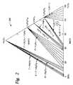
図1は、本発明の例示的な実施形態に従って生成されたタイプA及びタイプB材料を含
む様々なセラミック材料の電気抵抗率を示すグラフ100である。抵抗率は、軸102の
温度の関数として軸104に示される。抵抗率は、ASTM D1829−66又はJI
S C2141に準拠した標準試験条件を採用して空気環境内で1000Vで測定された。
ック材料を表す。Nb2O5を含む焼結セラミック材料に関して、許容可能な電気抵抗率
値は、図3の相図によって示されるように、追加の組成についても同様に得られることが
予測される。焼結セラミック材料は3種類の相を含み、Y2O3−ZrO2−Nb2O5
を含む第1相固溶体(焼結セラミック材料の約60モル%から約90モル%を構成する)
と、焼結セラミック材料の約5モル%から約30モル%を構成するY3NbO7の第2相
と元素形態のNbの第3相(焼結セラミック材料の約1モル%から約10モル%を構成す
る)が含まれる。この材料は、アーク放電を防止するのに抵抗率を低くする必要がある際
に特に有用である。抵抗率は、室温で約1011Ω・cm未満であり、200℃で約10
8Ω・cmであり、典型的な半導体処理条件下において109Ω・cmの範囲の抵抗率を
示す。
2−Y2O3として言及される。図3を参照すると、相図のある領域がBと分類されてい
る。この表示は、焼結セラミック材料の固溶体組成物が、Y2O3を濃度約55モル%〜
約80モル%、ZrO2を濃度約5モル%〜約25モル%、Nb2O5、HfO2、Nd
2O3又はSc2O3等の添加物を濃度約5モル%〜約25モル%で含むことを示してい
る。
図1の曲線108は、本発明に従って生成されたHfO2含有焼結セラミック材料を表
し、表においては試料1として記載されている。このセラミック材料は、Nb2O5含有
材料より高い抵抗率を示すが、静電チャック又は基板昇降ピンよりアーク放電が問題とな
らない半導体処理装置部品の作製に有用である。
図1の曲線110は、本発明に従って生成されたSc2O3含有焼結セラミック材料を
表し、表においては試料2として記載されている。ここでもまた、この材料は抵抗率要件
が1011Ω・cmである用途において使用され得る。
図1の曲線112は、図2の相図に図示されるY2O3−ZrO2−Al2O3材料を
表す。この材料は制御された抵抗率のセラミック材料に関してのみ比較例として説明され
る。この焼結セラミック材料は、Y2O3及びZrO2から成る固溶体及びY2O3及び
Al2O3酸化物から成る化合物を含む。典型的な焼結セラミック材料は、濃度約60モ
ル%〜約65モル%のY2O3、濃度約20モル%〜約25モル%のZrO2、濃度約1
0モル%〜約15モル%のAl2O3から生成される。図2の相図において領域Aとして
図示され、また図1においてY2O3−ZrO2−Al2O3についてのグラフによって
表される焼結セラミック材料の一実施形態は、立方晶イットリアタイプの結晶構造を有す
る約60モル%の固溶体(ここでc−Y2O3は溶媒であり、Zr2O3は溶質である)
と、ホタル石タイプの結晶構造を有する約2モル%の固溶体(ここでZrO2は溶媒であ
り、Y2O3は溶質である)と、約38モル%のYAM(Y4Al2O9)化合物を含有
する。
図1の曲線114は、表において試料3として記載のNd2O3含有焼結セラミック材
料を表す。この材料は、放電を防止するのに必要な要件を満たしておらず、本発明を構成
する独自のセラミック材料の一部ではない比較例であると見なされる。
図1の曲線116は、純粋なY2O3の焼結セラミックについて観察された電気抵抗特
性を表す。この材料もまた比較例であり、ベースラインとして有用であるが、これは多数
の半導体装置部品が純粋なY2O3から作製されているからである。純粋なY2O3の抵
抗率と比較すると、本発明によって達成される電気抵抗率における極めて著しい改善がわ
かる。
窒化アルミニウムを表す)及び曲線122(同じく低電気抵抗率を必要とする静電チャッ
ク及びその他の半導体処理装置の作製に使用される第2のドープ窒化アルミニウムを表す
)も図示されている。
図4は、多数の焼結セラミック試験試料についての、抵抗率試験中に印加された電圧の
関数としての電気抵抗率を示すグラス400である。抵抗率は軸404に、電圧は軸40
2に示される。試験温度は室温(約27℃)である。このグラフの目的は、抵抗率が低下
するように制御された本発明のコロージョン耐性セラミックの実施形態と、現行のドープ
窒化アルミニウムセラミックとの間における抵抗率の違いを示すことである。ドープ窒化
アルミニウムセラミックは若干低い抵抗率を有するが、そのコロージョン速度は、抵抗率
が低下するよう改質された酸化イットリウム含有セラミックのコロージョン速度より少な
くとも2倍速い。
アルミニウムセラミックを表す。曲線420は、静電チャック及びその他の低抵抗率の部
品の作製に使用される別のドープ窒化アルミニウムセラミックを表す。
を表す。抵抗率が低下するように改質されたこの酸化イットリウム含有材料は、AIN−
1として識別されたドープ窒化アルミニウムの抵抗率に極めて近い抵抗率を示す。しかし
ながら依然として、ドープ窒化アルミニウムのコロージョン速度は、図5の棒グラフ50
0により表されるように、曲線406で表される酸化イットリウム含有材料のコロージョ
ン速度より10倍も速い。
を表す。このセラミック材料は、Nb2O5含有材料より高い抵抗率を示し、室温におい
ては、プラズマアーク放電がより起こりやすい部品に関して推奨される範囲を超えた抵抗
率を示す。しかしながら、一部の半導体処理において存在する温度である200℃におい
て、抵抗率は、図1の曲線108で示されるように、許容範囲内におさまる。
表す。ここでもまた、この材料は、抵抗率要件が1011Ω・cmである用途において、
処理温度が200℃の場合に使用することができる。
を目的として、図4の曲線412は、図2に示すY2O3、ZrO2及びAl2O3を含
むセラミックタイプAの材料を表す。図1に示されるこのようなタイプA材料の一実施形
態は、約60モル%の立方晶イットリアタイプ構造体(c−Y2O3を溶媒、Zr2O3
を溶質とする)、約2モル%のホタル石タイプ構造固溶体(ZrO2を溶媒、Y2O3を
溶質とする)、約38モル%のYAM(Y4Al2O9)化合物を含有する。タイプAの
HPM材料は許容可能なコロージョン耐性及び賞賛に値する機械的性質を示すが、電気抵
抗率は所望の範囲の最高1011Ω・cmより著しく高い。図1の曲線112によって表
されるように、200℃でもこの通りである。この材料は、電気抵抗率を変えたコロージ
ョン耐性セラミックについての実施形態には含まれない。
有焼結セラミック材料を示す。この材料は、放電を防止するのに必要な要件を満たしてお
らず、本発明を構成する独自のセラミック材料の一部ではない比較例であると見なされる。
察された電気抵抗特性を表す。この材料もまた比較例であり、ベースラインとして有用で
あるが、これは多数の半導体装置部品が純粋なY2O3から作製されているからである。
純粋なY2O3の抵抗率と比較すると、本発明によって達成される電気抵抗率における極
めて著しい改善がわかる。
図5は、プラズマに曝露された様々な焼結セラミック材料についての、Y2O3のエロ
ージョン速度に正規化された平均エロージョン速度を示す棒グラフ500である。プラズ
マはCF4及びCHF3ソースガスから発生させた。プラズマ処理チャンバはアプライド
マテリアルズ社から入手可能なトレンチエッチのためのイネーブラであった。プラズマ源
電力は最高2000W、処理チャンバ圧力は10〜500mTorr、基板温度は約40
℃、時間は76時間であった。軸502は、エロージョン耐性について試験した様々な材
料を示す。Y2O3−10ZrO2と識別された試験片は、100重量部のY2O3を1
0重量部のZrO2と共に焼結することにより形成された焼結固溶体セラミック試験片を
表す。Nb2O5又はHfO2又はNd2O3又はSc2O3を含有すると識別された試
験片は、これらの材料のそれぞれを含有すると記載された表の組成物を表す。軸504に
示されるエロージョン速度を比較すると、抵抗率を変化させた酸化イットリウム含有焼結
セラミック材料のエロージョン速度は、基本的に純粋な酸化イットリウムのエロージョン
速度と同じであることを示す。更に、抵抗率を変化させた酸化イットリウム含有焼結セラ
ミックのエロージョン速度は、実質的にAl2O3、AlN、ZrO2、石英、W/Zr
C、B4C、SiC、半導体処理チャンバライナ用及び半導体処理装置内部部品用のハロ
ゲンプラズマコロージョン耐性材料を得るのに使用されてきたその他のセラミック材料の
エロージョン速度よりも良好である。
基づいて、プラズマ漏れ電流における紫外線の作用を見積もるための計算が行われた。(
半導体処理において使用される類の)プラズマ環境における紫外線は、電気抵抗率を変化
させた酸化イットリウム含有焼結セラミック材料の漏れ電流に影響しない。
セラミック材料及びHfO2タイプB焼結セラミック材料における漏れ電流に与える影響
についての研究は、これらの材料の電気的性能は、このような紫外線照射により影響され
ないことを示した。
て限定するものではないが、蓋、ライナ、ノズル、ガス分散プレート、シャワーヘッド、
静電チャック部品、シャドーフレーム、基板保持フレーム、処理キット、チャンバライナ
が含まれる。
インアノードアルファトーチ638)の概略断面図600である。図6に図示のこの特定
の装置は、エアロプラズマK.K.(日本、東京)から入手可能なAPS7000シリー
ズのエアロプラズマ溶射システムである。装置600は、以下の部品:第1DC主電極6
02、第1補助電極604、第1アルゴン源606、第1空気源608、溶射材料粉末源
610、カソードトーチ612、アクセレレータノズル614、プラズマアーク616、
第2DC主電極618、第2補助電極620、デュアルアノードトーチ622A及び62
2B、第2アルゴン源626、第2空気源(プラズマトリミング)628A及び628B
、第3アルゴン源636、プラズマジェット632、溶融粉末源634、溶射する母材源
624を含む。
チは熱負荷の半分を担う。ツインアノードトーチα638を使用して、高電圧を比較的低
い電流で得ることが可能なため、各トーチの熱負荷は低くなる。トーチの各ノズル及び電
極ロッドは別々に水冷され、アーク開始点及び終了点は不活性ガスにより保護されるため
、200時間以上に亘る安定した運転が確保され、消耗部品の寿命は伸び、メンテナンス
のコストが低下する。
され、溶射材料をアーク内に直接供給することが可能である。溶射材料は高温のアーク柱
により完全に溶融する。アーク開始点及び終了点は不活性ガスにより保護されるため、空
気又は酸素を、アクセレレータノズル614を通して導入されるプラズマガスに使用する
ことが可能である。
より溶射材料の溶融に貢献しないプラズマジェットの熱をトリムし、基板材料及び膜への
熱負荷を軽減し、短距離での溶射を可能にする。
上記の例示的な実施形態は本発明の範囲を限定することを意図しておらず、当業者なら、
本開示を考慮して、このような実施形態を発展させて以下の本発明の特許請求の範囲の主
題に対応させることが可能である。
Claims (8)
- 半導体処理装置内で使用される物品の表面上に皮膜を塗布し、これによってハロゲン含有プラズマへのエロージョン耐性を示し、前記皮膜表面上でのプラズマアーク放電の可能性を低下させる皮膜を提供する方法であって、
前記皮膜は、
約55モル%〜約80モル%の範囲の濃度の酸化イットリウムと、
約5モル%〜約25モル%の範囲の濃度の酸化ジルコニウムと、
約5モル%〜約25モル%の範囲の濃度の酸化アルミニウム、酸化ハフニウム、酸化ニオブ、酸化スカンジウム、酸化ネオジム、酸化サマリウム、及びこれらの組み合わせから成る群から選択される少なくとも1つの他の酸化物とから成る群から選択されるを含む少なくとも3つの前駆体酸化物から形成されるスパッタリングターゲットからスパッタ堆積され、前記前駆体材料酸化物の総モル%は100モル%を超えず、
純粋なY2O3と同等又はそれよりも低いフッ素含有プラズマ内でのエロージョン耐性を示すスパッタ堆積された皮膜を提供し、
1000Vで測定された電気抵抗率が、約100℃の温度で約1015Ω・cm以下、約200℃で1013Ω・cm以下を示すスパッタ堆積された皮膜を提供する方法。 - 前記スパッタリングターゲットは、約45モル%〜約80モル%の範囲で存在する酸化イットリウムと、約5モル%〜約25モル%の範囲で存在する酸化ジルコニウムと、約5モル%〜約25モル%の範囲で存在する酸化ニオブを含む前駆体酸化物から形成され、前記前駆体材料酸化物の総モル%は100モル%を超えない請求項1記載の方法。
- 前記スパッタリングターゲットは、約55モル%〜約80モル%の範囲で存在する酸化イットリウムと、約5モル%〜約25モル%の範囲で存在する酸化ジルコニウムと、約5モル%〜約25モル%の範囲で存在する酸化ネオジムを含む前駆体酸化物から形成され、前記前駆体材料酸化物の総モル%は100モル%を超えない請求項1記載の方法。
- 前記スパッタリングターゲットは、約55モル%〜約80モル%の範囲で存在する酸化イットリウムと、約5モル%〜約25モル%の範囲で存在する酸化ジルコニウムと、約5モル%〜約25モル%の範囲で存在する酸化スカンジウムを含む前駆体酸化物から形成され、前記前駆体材料酸化物の総モル%は100モル%を超えない請求項1記載の方法。
- 前記スパッタリングターゲットは、約55モル%〜約80モル%の範囲で存在する酸化イットリウムと、約5モル%〜約25モル%の範囲で存在する酸化ジルコニウムと、約5モル%〜約25モル%の範囲で存在する酸化ハフニウムを含む前駆体酸化物から形成され、前記前駆体材料酸化物の総モル%は100モル%を超えない請求項1記載の方法。
- 前記スパッタリングターゲットは、約55モル%〜約80モル%の範囲で存在する酸化イットリウムと、約5モル%〜約25モル%の範囲で存在する酸化ジルコニウムと、約5モル%〜約25モル%の範囲で存在する酸化アルミニウムを含む前駆体酸化物から形成され、前記前駆体材料酸化物の総モル%は100モル%を超えない請求項1記載の方法。
- 前記スパッタリングターゲットは、約60モル%〜約65モル%の範囲で存在する酸化イットリウムと、約20モル%〜約25モル%の範囲で存在する酸化ジルコニウムと、約10モル%〜約15モル%の範囲で存在する酸化アルミニウムを含む前駆体酸化物から形成される請求項1記載の方法。
- 前記スパッタリングターゲットは、c−Y2O3が溶媒、Zr2O3が溶質である立方晶イットリア型結晶構造を有する約60モル%の固溶体と、ZrO2が溶媒、Y2O3が溶質であるホタル石タイプの結晶構造を有する約2モル%の固溶体と、約38モル%のYAM(Y4Al2O9)化合物とを含有するセラミックス材料を含む請求項7記載の方法。
Applications Claiming Priority (2)
| Application Number | Priority Date | Filing Date | Title |
|---|---|---|---|
| US11/890,221 | 2007-08-02 | ||
| US11/890,221US20080213496A1 (en) | 2002-02-14 | 2007-08-02 | Method of coating semiconductor processing apparatus with protective yttrium-containing coatings |
Related Parent Applications (1)
| Application Number | Title | Priority Date | Filing Date |
|---|---|---|---|
| JP2010519236ADivisionJP5506678B2 (ja) | 2007-08-02 | 2008-07-30 | イットリウム含有保護皮膜による半導体処理装置の被覆方法 |
Publications (2)
| Publication Number | Publication Date |
|---|---|
| JP2014159637Atrue JP2014159637A (ja) | 2014-09-04 |
| JP5978236B2 JP5978236B2 (ja) | 2016-08-24 |
Family
ID=40304675
Family Applications (2)
| Application Number | Title | Priority Date | Filing Date |
|---|---|---|---|
| JP2010519236AActiveJP5506678B2 (ja) | 2007-08-02 | 2008-07-30 | イットリウム含有保護皮膜による半導体処理装置の被覆方法 |
| JP2014054887AExpired - Fee RelatedJP5978236B2 (ja) | 2007-08-02 | 2014-03-18 | イットリウム含有保護皮膜による半導体処理装置の被覆方法 |
Family Applications Before (1)
| Application Number | Title | Priority Date | Filing Date |
|---|---|---|---|
| JP2010519236AActiveJP5506678B2 (ja) | 2007-08-02 | 2008-07-30 | イットリウム含有保護皮膜による半導体処理装置の被覆方法 |
Country Status (6)
| Country | Link |
|---|---|
| US (1) | US20080213496A1 (ja) |
| JP (2) | JP5506678B2 (ja) |
| KR (1) | KR101491437B1 (ja) |
| CN (2) | CN101772589B (ja) |
| TW (1) | TWI441794B (ja) |
| WO (1) | WO2009017766A1 (ja) |
Cited By (2)
| Publication number | Priority date | Publication date | Assignee | Title |
|---|---|---|---|---|
| JP2022047018A (ja)* | 2020-09-11 | 2022-03-24 | 新光電気工業株式会社 | 静電チャック、基板固定装置及び基板固定装置の製造方法 |
| US11987503B2 (en) | 2019-04-26 | 2024-05-21 | Nippon Yttrium Co., Ltd. | Powder for film formation or sintering |
Families Citing this family (144)
| Publication number | Priority date | Publication date | Assignee | Title |
|---|---|---|---|---|
| US7371467B2 (en)* | 2002-01-08 | 2008-05-13 | Applied Materials, Inc. | Process chamber component having electroplated yttrium containing coating |
| US7479304B2 (en)* | 2002-02-14 | 2009-01-20 | Applied Materials, Inc. | Gas distribution plate fabricated from a solid yttrium oxide-comprising substrate |
| US20080213496A1 (en)* | 2002-02-14 | 2008-09-04 | Applied Materials, Inc. | Method of coating semiconductor processing apparatus with protective yttrium-containing coatings |
| US10242888B2 (en) | 2007-04-27 | 2019-03-26 | Applied Materials, Inc. | Semiconductor processing apparatus with a ceramic-comprising surface which exhibits fracture toughness and halogen plasma resistance |
| US10622194B2 (en) | 2007-04-27 | 2020-04-14 | Applied Materials, Inc. | Bulk sintered solid solution ceramic which exhibits fracture toughness and halogen plasma resistance |
| US8367227B2 (en)* | 2007-08-02 | 2013-02-05 | Applied Materials, Inc. | Plasma-resistant ceramics with controlled electrical resistivity |
| KR20090093819A (ko)* | 2008-02-28 | 2009-09-02 | 코바렌트 마테리얼 가부시키가이샤 | 플라즈마 처리 장치에 이용되는 소결체 및 부재 |
| CN102272344A (zh)* | 2008-11-04 | 2011-12-07 | 普莱克斯技术有限公司 | 用于半导体应用的热喷涂层 |
| US20100140222A1 (en)* | 2008-12-10 | 2010-06-10 | Sun Jennifer Y | Filled polymer composition for etch chamber component |
| US20110070811A1 (en)* | 2009-03-25 | 2011-03-24 | Applied Materials, Inc. | Point of use recycling system for cmp slurry |
| FR2944293B1 (fr)* | 2009-04-10 | 2012-05-18 | Saint Gobain Coating Solutions | Procede d'elaboration par projection thermique d'une cible |
| JP5710591B2 (ja)* | 2009-04-20 | 2015-04-30 | アプライド マテリアルズ インコーポレイテッドApplied Materials,Incorporated | プロセスチャンバ壁上にシリコンコーティングを使用した残留フッ素ラジカルの除去の促進 |
| JP5837733B2 (ja)* | 2009-04-24 | 2015-12-24 | 国立大学法人東北大学 | 水分発生用反応炉 |
| KR101101910B1 (ko)* | 2009-06-03 | 2012-01-02 | 한국과학기술연구원 | 반도체 제조 장비용 다성분계 열용사 코팅물질, 그 제조방법 및 코팅방법 |
| WO2011066314A1 (en)* | 2009-11-25 | 2011-06-03 | Green, Tweed Of Delaware, Inc. | Methods of coating substrate with plasma resistant coatings and related coated substrates |
| JP5692772B2 (ja)* | 2009-11-26 | 2015-04-01 | 国立大学法人東北大学 | 表面保護膜、接ガス部材、ガス処理装置及びメカニカルポンプ |
| JP5665408B2 (ja)* | 2010-08-04 | 2015-02-04 | 国立大学法人東北大学 | 水分発生用反応炉 |
| JP2012036053A (ja)* | 2010-08-10 | 2012-02-23 | Covalent Materials Corp | 耐食性部材 |
| EP2742525A4 (en) | 2011-08-10 | 2015-04-01 | Entegris Inc | AION-COATED SUBSTRATE WITH OPTIONAL YTTRIUM OXIDE COATING |
| US20130064973A1 (en)* | 2011-09-09 | 2013-03-14 | Taiwan Semiconductor Manufacturing Company, Ltd. | Chamber Conditioning Method |
| JP6261979B2 (ja) | 2011-09-26 | 2018-01-17 | 株式会社フジミインコーポレーテッド | 皮膜の形成方法 |
| US9670099B2 (en) | 2011-09-26 | 2017-06-06 | Fujimi Incorporated | Thermal spray powder and film that contain rare-earth element, and member provided with film |
| JP5526098B2 (ja)* | 2011-09-30 | 2014-06-18 | コバレントマテリアル株式会社 | 耐食性部材及びその製造方法 |
| CN103074563B (zh)* | 2011-10-26 | 2017-09-12 | 中国科学院微电子研究所 | 一种y2o3耐侵蚀陶瓷涂层的改进方法 |
| KR20140108307A (ko)* | 2011-12-28 | 2014-09-05 | 가부시키가이샤 후지미인코퍼레이티드 | 산화이트륨 피막 |
| US9034199B2 (en) | 2012-02-21 | 2015-05-19 | Applied Materials, Inc. | Ceramic article with reduced surface defect density and process for producing a ceramic article |
| US9212099B2 (en) | 2012-02-22 | 2015-12-15 | Applied Materials, Inc. | Heat treated ceramic substrate having ceramic coating and heat treatment for coated ceramics |
| US9090046B2 (en)* | 2012-04-16 | 2015-07-28 | Applied Materials, Inc. | Ceramic coated article and process for applying ceramic coating |
| US9394615B2 (en)* | 2012-04-27 | 2016-07-19 | Applied Materials, Inc. | Plasma resistant ceramic coated conductive article |
| US9604249B2 (en)* | 2012-07-26 | 2017-03-28 | Applied Materials, Inc. | Innovative top-coat approach for advanced device on-wafer particle performance |
| US9343289B2 (en)* | 2012-07-27 | 2016-05-17 | Applied Materials, Inc. | Chemistry compatible coating material for advanced device on-wafer particle performance |
| US9132436B2 (en) | 2012-09-21 | 2015-09-15 | Applied Materials, Inc. | Chemical control features in wafer process equipment |
| CN103866286B (zh)* | 2012-12-18 | 2016-12-28 | 中微半导体设备(上海)有限公司 | 用于半导体基片反应室内部的部件及制造方法 |
| US10256079B2 (en) | 2013-02-08 | 2019-04-09 | Applied Materials, Inc. | Semiconductor processing systems having multiple plasma configurations |
| US9362130B2 (en) | 2013-03-01 | 2016-06-07 | Applied Materials, Inc. | Enhanced etching processes using remote plasma sources |
| US9708713B2 (en) | 2013-05-24 | 2017-07-18 | Applied Materials, Inc. | Aerosol deposition coating for semiconductor chamber components |
| US9865434B2 (en)* | 2013-06-05 | 2018-01-09 | Applied Materials, Inc. | Rare-earth oxide based erosion resistant coatings for semiconductor application |
| US9850568B2 (en) | 2013-06-20 | 2017-12-26 | Applied Materials, Inc. | Plasma erosion resistant rare-earth oxide based thin film coatings |
| US9711334B2 (en)* | 2013-07-19 | 2017-07-18 | Applied Materials, Inc. | Ion assisted deposition for rare-earth oxide based thin film coatings on process rings |
| US9583369B2 (en) | 2013-07-20 | 2017-02-28 | Applied Materials, Inc. | Ion assisted deposition for rare-earth oxide based coatings on lids and nozzles |
| US9624593B2 (en)* | 2013-08-29 | 2017-04-18 | Applied Materials, Inc. | Anodization architecture for electro-plate adhesion |
| US20150079370A1 (en)* | 2013-09-18 | 2015-03-19 | Applied Materials, Inc. | Coating architecture for plasma sprayed chamber components |
| US9440886B2 (en)* | 2013-11-12 | 2016-09-13 | Applied Materials, Inc. | Rare-earth oxide based monolithic chamber material |
| SG10201804237VA (en) | 2013-11-21 | 2018-06-28 | Entegris Inc | Surface coating for chamber components used in plasma systems |
| US9725799B2 (en) | 2013-12-06 | 2017-08-08 | Applied Materials, Inc. | Ion beam sputtering with ion assisted deposition for coatings on chamber components |
| JP6221818B2 (ja)* | 2014-02-25 | 2017-11-01 | 日本ゼオン株式会社 | グラビア塗工装置 |
| US9869013B2 (en)* | 2014-04-25 | 2018-01-16 | Applied Materials, Inc. | Ion assisted deposition top coat of rare-earth oxide |
| US9976211B2 (en) | 2014-04-25 | 2018-05-22 | Applied Materials, Inc. | Plasma erosion resistant thin film coating for high temperature application |
| US10730798B2 (en)* | 2014-05-07 | 2020-08-04 | Applied Materials, Inc. | Slurry plasma spray of plasma resistant ceramic coating |
| US10196728B2 (en)* | 2014-05-16 | 2019-02-05 | Applied Materials, Inc. | Plasma spray coating design using phase and stress control |
| US9309598B2 (en) | 2014-05-28 | 2016-04-12 | Applied Materials, Inc. | Oxide and metal removal |
| CN105225923B (zh)* | 2014-05-29 | 2019-11-26 | 上海矽睿科技有限公司 | 用于键合的铝材料的预处理方法及键合方法 |
| US10266943B2 (en) | 2014-06-27 | 2019-04-23 | Applied Materials, Inc. | Plasma corrosion resistive heater for high temperature processing |
| KR102437125B1 (ko)* | 2014-06-27 | 2022-08-25 | 어플라이드 머티어리얼스, 인코포레이티드 | 고온 프로세싱을 위한 플라즈마 부식 저항성 가열기 |
| JP6634371B2 (ja)* | 2014-06-30 | 2020-01-22 | 日本碍子株式会社 | MgO系セラミックス膜、半導体製造装置用部材及びMgO系セラミックス膜の製法 |
| US9460898B2 (en) | 2014-08-08 | 2016-10-04 | Applied Materials, Inc. | Plasma generation chamber with smooth plasma resistant coating |
| KR101465640B1 (ko)* | 2014-08-08 | 2014-11-28 | 주식회사 펨빅스 | 불화알루미늄 생성방지막이 형성된 cvd 공정챔버 부품 |
| US9355922B2 (en) | 2014-10-14 | 2016-05-31 | Applied Materials, Inc. | Systems and methods for internal surface conditioning in plasma processing equipment |
| US9966240B2 (en)* | 2014-10-14 | 2018-05-08 | Applied Materials, Inc. | Systems and methods for internal surface conditioning assessment in plasma processing equipment |
| US11637002B2 (en) | 2014-11-26 | 2023-04-25 | Applied Materials, Inc. | Methods and systems to enhance process uniformity |
| US10573496B2 (en) | 2014-12-09 | 2020-02-25 | Applied Materials, Inc. | Direct outlet toroidal plasma source |
| US20160225652A1 (en) | 2015-02-03 | 2016-08-04 | Applied Materials, Inc. | Low temperature chuck for plasma processing systems |
| US9728437B2 (en) | 2015-02-03 | 2017-08-08 | Applied Materials, Inc. | High temperature chuck for plasma processing systems |
| CN105986245A (zh)* | 2015-02-16 | 2016-10-05 | 中微半导体设备(上海)有限公司 | 改善mocvd反应工艺的部件及改善方法 |
| US20160254125A1 (en)* | 2015-02-27 | 2016-09-01 | Lam Research Corporation | Method for coating surfaces |
| JP6350380B2 (ja)* | 2015-04-28 | 2018-07-04 | 信越化学工業株式会社 | 希土類磁石の製造方法 |
| US9741593B2 (en) | 2015-08-06 | 2017-08-22 | Applied Materials, Inc. | Thermal management systems and methods for wafer processing systems |
| US9691645B2 (en) | 2015-08-06 | 2017-06-27 | Applied Materials, Inc. | Bolted wafer chuck thermal management systems and methods for wafer processing systems |
| US9349605B1 (en) | 2015-08-07 | 2016-05-24 | Applied Materials, Inc. | Oxide etch selectivity systems and methods |
| US10504700B2 (en) | 2015-08-27 | 2019-12-10 | Applied Materials, Inc. | Plasma etching systems and methods with secondary plasma injection |
| JP6668024B2 (ja)* | 2015-09-25 | 2020-03-18 | 株式会社フジミインコーポレーテッド | 溶射材料 |
| FR3043679B1 (fr)* | 2015-11-12 | 2021-07-23 | Aptar Stelmi Sas | Procede de traitement d'un element de conditionnement en elastomere, et element de conditionnement ainsi traite. |
| WO2017128171A1 (zh)* | 2016-01-28 | 2017-08-03 | 深圳市商德先进陶瓷股份有限公司 | 耐等离子刻蚀陶瓷体及其制造方法、等离子刻蚀设备 |
| WO2017155711A1 (en)* | 2016-03-11 | 2017-09-14 | Applied Materials, Inc. | Method for electrochemically grown yttria or yttrium oxide on semiconductor processing equipment |
| US11326253B2 (en) | 2016-04-27 | 2022-05-10 | Applied Materials, Inc. | Atomic layer deposition of protective coatings for semiconductor process chamber components |
| US10522371B2 (en) | 2016-05-19 | 2019-12-31 | Applied Materials, Inc. | Systems and methods for improved semiconductor etching and component protection |
| US10504754B2 (en) | 2016-05-19 | 2019-12-10 | Applied Materials, Inc. | Systems and methods for improved semiconductor etching and component protection |
| US9850573B1 (en)* | 2016-06-23 | 2017-12-26 | Applied Materials, Inc. | Non-line of sight deposition of erbium based plasma resistant ceramic coating |
| US9865484B1 (en) | 2016-06-29 | 2018-01-09 | Applied Materials, Inc. | Selective etch using material modification and RF pulsing |
| US20180016678A1 (en) | 2016-07-15 | 2018-01-18 | Applied Materials, Inc. | Multi-layer coating with diffusion barrier layer and erosion resistant layer |
| US10629473B2 (en) | 2016-09-09 | 2020-04-21 | Applied Materials, Inc. | Footing removal for nitride spacer |
| US10546729B2 (en) | 2016-10-04 | 2020-01-28 | Applied Materials, Inc. | Dual-channel showerhead with improved profile |
| US9934942B1 (en) | 2016-10-04 | 2018-04-03 | Applied Materials, Inc. | Chamber with flow-through source |
| JP6650385B2 (ja) | 2016-11-07 | 2020-02-19 | 東京エレクトロン株式会社 | 溶射用材料、溶射皮膜および溶射皮膜付部材 |
| US10163696B2 (en) | 2016-11-11 | 2018-12-25 | Applied Materials, Inc. | Selective cobalt removal for bottom up gapfill |
| US10026621B2 (en) | 2016-11-14 | 2018-07-17 | Applied Materials, Inc. | SiN spacer profile patterning |
| US10566206B2 (en) | 2016-12-27 | 2020-02-18 | Applied Materials, Inc. | Systems and methods for anisotropic material breakthrough |
| US10186400B2 (en) | 2017-01-20 | 2019-01-22 | Applied Materials, Inc. | Multi-layer plasma resistant coating by atomic layer deposition |
| US10431429B2 (en) | 2017-02-03 | 2019-10-01 | Applied Materials, Inc. | Systems and methods for radial and azimuthal control of plasma uniformity |
| US10319739B2 (en) | 2017-02-08 | 2019-06-11 | Applied Materials, Inc. | Accommodating imperfectly aligned memory holes |
| US10943834B2 (en) | 2017-03-13 | 2021-03-09 | Applied Materials, Inc. | Replacement contact process |
| US10975469B2 (en) | 2017-03-17 | 2021-04-13 | Applied Materials, Inc. | Plasma resistant coating of porous body by atomic layer deposition |
| US20180327892A1 (en)* | 2017-05-10 | 2018-11-15 | Applied Materials, Inc. | Metal oxy-flouride films for chamber components |
| US11276559B2 (en) | 2017-05-17 | 2022-03-15 | Applied Materials, Inc. | Semiconductor processing chamber for multiple precursor flow |
| JP7176860B6 (ja) | 2017-05-17 | 2022-12-16 | アプライド マテリアルズ インコーポレイテッド | 前駆体の流れを改善する半導体処理チャンバ |
| US11276590B2 (en) | 2017-05-17 | 2022-03-15 | Applied Materials, Inc. | Multi-zone semiconductor substrate supports |
| US10497579B2 (en) | 2017-05-31 | 2019-12-03 | Applied Materials, Inc. | Water-free etching methods |
| US10920320B2 (en) | 2017-06-16 | 2021-02-16 | Applied Materials, Inc. | Plasma health determination in semiconductor substrate processing reactors |
| US10541246B2 (en) | 2017-06-26 | 2020-01-21 | Applied Materials, Inc. | 3D flash memory cells which discourage cross-cell electrical tunneling |
| US10727080B2 (en) | 2017-07-07 | 2020-07-28 | Applied Materials, Inc. | Tantalum-containing material removal |
| US10541184B2 (en) | 2017-07-11 | 2020-01-21 | Applied Materials, Inc. | Optical emission spectroscopic techniques for monitoring etching |
| US10043674B1 (en) | 2017-08-04 | 2018-08-07 | Applied Materials, Inc. | Germanium etching systems and methods |
| US10297458B2 (en) | 2017-08-07 | 2019-05-21 | Applied Materials, Inc. | Process window widening using coated parts in plasma etch processes |
| US11279656B2 (en) | 2017-10-27 | 2022-03-22 | Applied Materials, Inc. | Nanopowders, nanoceramic materials and methods of making and use thereof |
| US10766824B2 (en)* | 2017-11-08 | 2020-09-08 | Applied Materials, Inc. | Methods of minimizing particles on wafer from plasma spray coatings |
| US10903054B2 (en) | 2017-12-19 | 2021-01-26 | Applied Materials, Inc. | Multi-zone gas distribution systems and methods |
| US11328909B2 (en) | 2017-12-22 | 2022-05-10 | Applied Materials, Inc. | Chamber conditioning and removal processes |
| US10854426B2 (en) | 2018-01-08 | 2020-12-01 | Applied Materials, Inc. | Metal recess for semiconductor structures |
| US10679870B2 (en) | 2018-02-15 | 2020-06-09 | Applied Materials, Inc. | Semiconductor processing chamber multistage mixing apparatus |
| US10964512B2 (en) | 2018-02-15 | 2021-03-30 | Applied Materials, Inc. | Semiconductor processing chamber multistage mixing apparatus and methods |
| US11047035B2 (en) | 2018-02-23 | 2021-06-29 | Applied Materials, Inc. | Protective yttria coating for semiconductor equipment parts |
| TWI766433B (zh) | 2018-02-28 | 2022-06-01 | 美商應用材料股份有限公司 | 形成氣隙的系統及方法 |
| US10593560B2 (en) | 2018-03-01 | 2020-03-17 | Applied Materials, Inc. | Magnetic induction plasma source for semiconductor processes and equipment |
| US10319600B1 (en) | 2018-03-12 | 2019-06-11 | Applied Materials, Inc. | Thermal silicon etch |
| US10497573B2 (en) | 2018-03-13 | 2019-12-03 | Applied Materials, Inc. | Selective atomic layer etching of semiconductor materials |
| US10573527B2 (en) | 2018-04-06 | 2020-02-25 | Applied Materials, Inc. | Gas-phase selective etching systems and methods |
| US10443126B1 (en) | 2018-04-06 | 2019-10-15 | Applied Materials, Inc. | Zone-controlled rare-earth oxide ALD and CVD coatings |
| US10490406B2 (en) | 2018-04-10 | 2019-11-26 | Appled Materials, Inc. | Systems and methods for material breakthrough |
| US10699879B2 (en) | 2018-04-17 | 2020-06-30 | Applied Materials, Inc. | Two piece electrode assembly with gap for plasma control |
| US10886137B2 (en) | 2018-04-30 | 2021-01-05 | Applied Materials, Inc. | Selective nitride removal |
| US11401599B2 (en) | 2018-06-18 | 2022-08-02 | Applied Materials, Inc. | Erosion resistant metal silicate coatings |
| US10872778B2 (en) | 2018-07-06 | 2020-12-22 | Applied Materials, Inc. | Systems and methods utilizing solid-phase etchants |
| US10755941B2 (en) | 2018-07-06 | 2020-08-25 | Applied Materials, Inc. | Self-limiting selective etching systems and methods |
| US11667575B2 (en) | 2018-07-18 | 2023-06-06 | Applied Materials, Inc. | Erosion resistant metal oxide coatings |
| US10672642B2 (en) | 2018-07-24 | 2020-06-02 | Applied Materials, Inc. | Systems and methods for pedestal configuration |
| US10892198B2 (en) | 2018-09-14 | 2021-01-12 | Applied Materials, Inc. | Systems and methods for improved performance in semiconductor processing |
| US11049755B2 (en) | 2018-09-14 | 2021-06-29 | Applied Materials, Inc. | Semiconductor substrate supports with embedded RF shield |
| US11062887B2 (en) | 2018-09-17 | 2021-07-13 | Applied Materials, Inc. | High temperature RF heater pedestals |
| US11417534B2 (en) | 2018-09-21 | 2022-08-16 | Applied Materials, Inc. | Selective material removal |
| US11682560B2 (en) | 2018-10-11 | 2023-06-20 | Applied Materials, Inc. | Systems and methods for hafnium-containing film removal |
| US11121002B2 (en) | 2018-10-24 | 2021-09-14 | Applied Materials, Inc. | Systems and methods for etching metals and metal derivatives |
| US11437242B2 (en) | 2018-11-27 | 2022-09-06 | Applied Materials, Inc. | Selective removal of silicon-containing materials |
| US11180847B2 (en) | 2018-12-06 | 2021-11-23 | Applied Materials, Inc. | Atomic layer deposition coatings for high temperature ceramic components |
| DE102018221940A1 (de)* | 2018-12-17 | 2020-06-18 | Siemens Aktiengesellschaft | Keramisches Material, Schicht und Schichtsystem |
| US11721527B2 (en) | 2019-01-07 | 2023-08-08 | Applied Materials, Inc. | Processing chamber mixing systems |
| US10920319B2 (en) | 2019-01-11 | 2021-02-16 | Applied Materials, Inc. | Ceramic showerheads with conductive electrodes |
| US10858741B2 (en) | 2019-03-11 | 2020-12-08 | Applied Materials, Inc. | Plasma resistant multi-layer architecture for high aspect ratio parts |
| CN110004393A (zh)* | 2019-04-08 | 2019-07-12 | 中国科学院金属研究所 | 一种超音速火焰喷涂技术制备y2o3陶瓷涂层的方法 |
| US11547030B2 (en)* | 2019-09-26 | 2023-01-03 | Applied Materials, Inc. | Ultrathin conformal coatings for electrostatic dissipation in semiconductor process tools |
| CN112899617B (zh)* | 2019-12-04 | 2023-03-31 | 中微半导体设备(上海)股份有限公司 | 形成耐等离子体涂层的方法、装置、零部件和等离子体处理装置 |
| EP4179127A4 (en)* | 2020-07-09 | 2025-04-02 | Entegris, Inc. | Coatings with fluorinated yttrium oxide and a metal oxide, and methods for producing and using the coatings |
| CN118043492A (zh) | 2021-12-10 | 2024-05-14 | 东华隆株式会社 | 适于等离子体蚀刻装置用构件等的成膜材料及其制造方法 |
| US12392932B2 (en) | 2022-07-15 | 2025-08-19 | University Of North Texas | Ultralow emittance metasurface thermal radiation barriers |
| CN116199514B (zh)* | 2023-02-28 | 2024-04-23 | 常州市卓群纳米新材料有限公司 | 液相等离子喷涂高纯氧化钇悬浮液及其制备方法 |
Citations (9)
| Publication number | Priority date | Publication date | Assignee | Title |
|---|---|---|---|---|
| JPH09232301A (ja)* | 1996-02-26 | 1997-09-05 | Sumitomo Sitix Corp | 半導体製造装置 |
| JP2001102365A (ja)* | 1999-07-29 | 2001-04-13 | Kyocera Corp | 真空容器及びその製造方法 |
| JP2002037683A (ja)* | 2000-07-24 | 2002-02-06 | Toshiba Ceramics Co Ltd | 耐プラズマ性部材およびその製造方法 |
| JP2002087878A (ja)* | 2000-07-11 | 2002-03-27 | Toshiba Ceramics Co Ltd | 耐プラズマ性部材およびその製造方法 |
| JP2002249864A (ja)* | 2000-04-18 | 2002-09-06 | Ngk Insulators Ltd | 耐ハロゲンガスプラズマ用部材およびその製造方法 |
| JP2003095649A (ja)* | 2001-07-19 | 2003-04-03 | Ngk Insulators Ltd | イットリア−アルミナ複合酸化物膜の製造方法、イットリア−アルミナ複合酸化物膜、溶射膜、耐蝕性部材および低パーティクル部材 |
| JP2004523649A (ja)* | 2000-12-29 | 2004-08-05 | ラム リサーチ コーポレーション | 半導体処理装置の窒化ホウ素又はイットリア複合材料の構成部品及びその製造方法 |
| JP2004241203A (ja)* | 2003-02-04 | 2004-08-26 | Hitachi High-Technologies Corp | プラズマ処理室壁処理方法 |
| JP2010535288A (ja)* | 2007-08-02 | 2010-11-18 | アプライド マテリアルズ インコーポレイテッド | イットリウム含有保護皮膜による半導体処理装置の被覆方法 |
Family Cites Families (59)
| Publication number | Priority date | Publication date | Assignee | Title |
|---|---|---|---|---|
| SU381643A1 (ru)* | 1971-03-22 | 1973-05-22 | Ордена Трудового Красного Знамени институт проблем материаловедени Украинской ССР | Высокоогнеупорный керамический материал |
| US4166880A (en)* | 1978-01-18 | 1979-09-04 | Solamat Incorporated | Solar energy device |
| US4576874A (en)* | 1984-10-03 | 1986-03-18 | Westinghouse Electric Corp. | Spalling and corrosion resistant ceramic coating for land and marine combustion turbines |
| US20030152813A1 (en)* | 1992-10-23 | 2003-08-14 | Symetrix Corporation | Lanthanide series layered superlattice materials for integrated circuit appalications |
| US5366585A (en)* | 1993-01-28 | 1994-11-22 | Applied Materials, Inc. | Method and apparatus for protection of conductive surfaces in a plasma processing reactor |
| JPH07122500A (ja)* | 1993-10-28 | 1995-05-12 | Fujitsu Ltd | ガス機器及びこれを利用したガス供給装置 |
| US5798016A (en)* | 1994-03-08 | 1998-08-25 | International Business Machines Corporation | Apparatus for hot wall reactive ion etching using a dielectric or metallic liner with temperature control to achieve process stability |
| US5680013A (en)* | 1994-03-15 | 1997-10-21 | Applied Materials, Inc. | Ceramic protection for heated metal surfaces of plasma processing chamber exposed to chemically aggressive gaseous environment therein and method of protecting such heated metal surfaces |
| US5605637A (en)* | 1994-12-15 | 1997-02-25 | Applied Materials Inc. | Adjustable dc bias control in a plasma reactor |
| EP0722919B1 (en)* | 1995-01-19 | 1999-08-11 | Ube Industries, Ltd. | Ceramic composite |
| US6447937B1 (en)* | 1997-02-26 | 2002-09-10 | Kyocera Corporation | Ceramic materials resistant to halogen plasma and components using the same |
| US5942039A (en)* | 1997-05-01 | 1999-08-24 | Applied Materials, Inc. | Self-cleaning focus ring |
| JP2003526191A (ja)* | 1997-08-13 | 2003-09-02 | アプライド マテリアルズ インコーポレイテッド | 半導体デバイス用銅エッチング方法 |
| US6123791A (en)* | 1998-07-29 | 2000-09-26 | Applied Materials, Inc. | Ceramic composition for an apparatus and method for processing a substrate |
| US6170429B1 (en)* | 1998-09-30 | 2001-01-09 | Lam Research Corporation | Chamber liner for semiconductor process chambers |
| TW465017B (en)* | 1999-04-13 | 2001-11-21 | Applied Materials Inc | A corrosion-resistant protective coating for an apparatus and method for processing a substrate |
| US6408786B1 (en)* | 1999-09-23 | 2002-06-25 | Lam Research Corporation | Semiconductor processing equipment having tiled ceramic liner |
| KR20010062209A (ko)* | 1999-12-10 | 2001-07-07 | 히가시 데쓰로 | 고내식성 막이 내부에 형성된 챔버를 구비하는 처리 장치 |
| JP3510993B2 (ja)* | 1999-12-10 | 2004-03-29 | トーカロ株式会社 | プラズマ処理容器内部材およびその製造方法 |
| US20020110698A1 (en)* | 1999-12-14 | 2002-08-15 | Jogender Singh | Thermal barrier coatings and electron-beam, physical vapor deposition for making same |
| US6521046B2 (en)* | 2000-02-04 | 2003-02-18 | Kabushiki Kaisha Kobe Seiko Sho | Chamber material made of Al alloy and heater block |
| TW503449B (en)* | 2000-04-18 | 2002-09-21 | Ngk Insulators Ltd | Halogen gas plasma-resistive members and method for producing the same, laminates, and corrosion-resistant members |
| JP2001308011A (ja)* | 2000-04-18 | 2001-11-02 | Ngk Insulators Ltd | 半導体製造装置用チャンバー部材 |
| US6645585B2 (en)* | 2000-05-30 | 2003-11-11 | Kyocera Corporation | Container for treating with corrosive-gas and plasma and method for manufacturing the same |
| JP3967093B2 (ja)* | 2000-07-10 | 2007-08-29 | 東芝セラミックス株式会社 | セラミックス部材およびその製造方法 |
| JP2002356387A (ja)* | 2001-03-30 | 2002-12-13 | Toshiba Ceramics Co Ltd | 耐プラズマ性部材 |
| US6830622B2 (en)* | 2001-03-30 | 2004-12-14 | Lam Research Corporation | Cerium oxide containing ceramic components and coatings in semiconductor processing equipment and methods of manufacture thereof |
| CN1309859C (zh)* | 2001-05-17 | 2007-04-11 | 东京电子株式会社 | 基于圆筒的等离子体处理系统 |
| US6682627B2 (en)* | 2001-09-24 | 2004-01-27 | Applied Materials, Inc. | Process chamber having a corrosion-resistant wall and method |
| JP2003146751A (ja)* | 2001-11-20 | 2003-05-21 | Toshiba Ceramics Co Ltd | 耐プラズマ性部材及びその製造方法 |
| US7371467B2 (en)* | 2002-01-08 | 2008-05-13 | Applied Materials, Inc. | Process chamber component having electroplated yttrium containing coating |
| US6942929B2 (en)* | 2002-01-08 | 2005-09-13 | Nianci Han | Process chamber having component with yttrium-aluminum coating |
| US20080264564A1 (en)* | 2007-04-27 | 2008-10-30 | Applied Materials, Inc. | Method of reducing the erosion rate of semiconductor processing apparatus exposed to halogen-containing plasmas |
| US6776873B1 (en)* | 2002-02-14 | 2004-08-17 | Jennifer Y Sun | Yttrium oxide based surface coating for semiconductor IC processing vacuum chambers |
| US8067067B2 (en)* | 2002-02-14 | 2011-11-29 | Applied Materials, Inc. | Clean, dense yttrium oxide coating protecting semiconductor processing apparatus |
| US7479304B2 (en)* | 2002-02-14 | 2009-01-20 | Applied Materials, Inc. | Gas distribution plate fabricated from a solid yttrium oxide-comprising substrate |
| JP2003257321A (ja)* | 2002-03-06 | 2003-09-12 | Pioneer Electronic Corp | プラズマディスプレイパネル |
| US6780787B2 (en)* | 2002-03-21 | 2004-08-24 | Lam Research Corporation | Low contamination components for semiconductor processing apparatus and methods for making components |
| US6565984B1 (en)* | 2002-05-28 | 2003-05-20 | Applied Materials Inc. | Clean aluminum alloy for semiconductor processing equipment |
| US7147749B2 (en)* | 2002-09-30 | 2006-12-12 | Tokyo Electron Limited | Method and apparatus for an improved upper electrode plate with deposition shield in a plasma processing system |
| US6798519B2 (en)* | 2002-09-30 | 2004-09-28 | Tokyo Electron Limited | Method and apparatus for an improved optical window deposition shield in a plasma processing system |
| US7137353B2 (en)* | 2002-09-30 | 2006-11-21 | Tokyo Electron Limited | Method and apparatus for an improved deposition shield in a plasma processing system |
| US7166166B2 (en)* | 2002-09-30 | 2007-01-23 | Tokyo Electron Limited | Method and apparatus for an improved baffle plate in a plasma processing system |
| US7166200B2 (en)* | 2002-09-30 | 2007-01-23 | Tokyo Electron Limited | Method and apparatus for an improved upper electrode plate in a plasma processing system |
| US20040245098A1 (en)* | 2003-06-04 | 2004-12-09 | Rodger Eckerson | Method of fabricating a shield |
| CN1288108C (zh)* | 2003-10-24 | 2006-12-06 | 东芝陶瓷股份有限会社 | 耐等离子体构件、其制造方法及形成热喷涂涂层的方法 |
| US20050123288A1 (en)* | 2003-11-12 | 2005-06-09 | Ibiden Co., Ltd. | Gas injection head, method for manufacturing the same, semiconductor manufacturing device with the gas injection head and anti-corrosion product |
| US6983892B2 (en)* | 2004-02-05 | 2006-01-10 | Applied Materials, Inc. | Gas distribution showerhead for semiconductor processing |
| US7135426B2 (en)* | 2004-05-25 | 2006-11-14 | Applied Materials, Inc. | Erosion resistant process chamber components |
| US20050279457A1 (en)* | 2004-06-04 | 2005-12-22 | Tokyo Electron Limited | Plasma processing apparatus and method, and plasma control unit |
| US20060042754A1 (en)* | 2004-07-30 | 2006-03-02 | Tokyo Electron Limited | Plasma etching apparatus |
| US7119032B2 (en)* | 2004-08-23 | 2006-10-10 | Air Products And Chemicals, Inc. | Method to protect internal components of semiconductor processing equipment using layered superlattice materials |
| US20060043067A1 (en)* | 2004-08-26 | 2006-03-02 | Lam Research Corporation | Yttria insulator ring for use inside a plasma chamber |
| JP2006097114A (ja)* | 2004-09-30 | 2006-04-13 | Tosoh Corp | 耐蝕性溶射膜部材 |
| JP2006186306A (ja)* | 2004-09-30 | 2006-07-13 | Toshiba Ceramics Co Ltd | ガス拡散プレートおよびその製造方法 |
| KR100910261B1 (ko)* | 2005-10-31 | 2009-07-31 | 코바렌트 마테리얼 가부시키가이샤 | 투광성 희토류 산화 소결체 및 그 제조 방법 |
| US7248457B2 (en)* | 2005-11-15 | 2007-07-24 | Toto Ltd. | Electrostatic chuck |
| US7696117B2 (en)* | 2007-04-27 | 2010-04-13 | Applied Materials, Inc. | Method and apparatus which reduce the erosion rate of surfaces exposed to halogen-containing plasmas |
| US20090214825A1 (en)* | 2008-02-26 | 2009-08-27 | Applied Materials, Inc. | Ceramic coating comprising yttrium which is resistant to a reducing plasma |
- 2007
- 2007-08-02USUS11/890,221patent/US20080213496A1/ennot_activeAbandoned
- 2008
- 2008-07-30KRKR1020107004581Apatent/KR101491437B1/konot_activeExpired - Fee Related
- 2008-07-30CNCN2008801016758Apatent/CN101772589B/zhnot_activeExpired - Fee Related
- 2008-07-30CNCN201310323450XApatent/CN103436836A/zhactivePending
- 2008-07-30WOPCT/US2008/009221patent/WO2009017766A1/enactiveApplication Filing
- 2008-07-30JPJP2010519236Apatent/JP5506678B2/jaactiveActive
- 2008-08-01TWTW097129360Apatent/TWI441794B/zhnot_activeIP Right Cessation
- 2014
- 2014-03-18JPJP2014054887Apatent/JP5978236B2/janot_activeExpired - Fee Related
Patent Citations (9)
| Publication number | Priority date | Publication date | Assignee | Title |
|---|---|---|---|---|
| JPH09232301A (ja)* | 1996-02-26 | 1997-09-05 | Sumitomo Sitix Corp | 半導体製造装置 |
| JP2001102365A (ja)* | 1999-07-29 | 2001-04-13 | Kyocera Corp | 真空容器及びその製造方法 |
| JP2002249864A (ja)* | 2000-04-18 | 2002-09-06 | Ngk Insulators Ltd | 耐ハロゲンガスプラズマ用部材およびその製造方法 |
| JP2002087878A (ja)* | 2000-07-11 | 2002-03-27 | Toshiba Ceramics Co Ltd | 耐プラズマ性部材およびその製造方法 |
| JP2002037683A (ja)* | 2000-07-24 | 2002-02-06 | Toshiba Ceramics Co Ltd | 耐プラズマ性部材およびその製造方法 |
| JP2004523649A (ja)* | 2000-12-29 | 2004-08-05 | ラム リサーチ コーポレーション | 半導体処理装置の窒化ホウ素又はイットリア複合材料の構成部品及びその製造方法 |
| JP2003095649A (ja)* | 2001-07-19 | 2003-04-03 | Ngk Insulators Ltd | イットリア−アルミナ複合酸化物膜の製造方法、イットリア−アルミナ複合酸化物膜、溶射膜、耐蝕性部材および低パーティクル部材 |
| JP2004241203A (ja)* | 2003-02-04 | 2004-08-26 | Hitachi High-Technologies Corp | プラズマ処理室壁処理方法 |
| JP2010535288A (ja)* | 2007-08-02 | 2010-11-18 | アプライド マテリアルズ インコーポレイテッド | イットリウム含有保護皮膜による半導体処理装置の被覆方法 |
Cited By (3)
| Publication number | Priority date | Publication date | Assignee | Title |
|---|---|---|---|---|
| US11987503B2 (en) | 2019-04-26 | 2024-05-21 | Nippon Yttrium Co., Ltd. | Powder for film formation or sintering |
| JP2022047018A (ja)* | 2020-09-11 | 2022-03-24 | 新光電気工業株式会社 | 静電チャック、基板固定装置及び基板固定装置の製造方法 |
| JP7438070B2 (ja) | 2020-09-11 | 2024-02-26 | 新光電気工業株式会社 | 静電チャック、基板固定装置及び基板固定装置の製造方法 |
Also Published As
| Publication number | Publication date |
|---|---|
| TWI441794B (zh) | 2014-06-21 |
| CN103436836A (zh) | 2013-12-11 |
| JP5506678B2 (ja) | 2014-05-28 |
| TW200914394A (en) | 2009-04-01 |
| KR20100052502A (ko) | 2010-05-19 |
| CN101772589A (zh) | 2010-07-07 |
| KR101491437B1 (ko) | 2015-02-10 |
| JP2010535288A (ja) | 2010-11-18 |
| JP5978236B2 (ja) | 2016-08-24 |
| CN101772589B (zh) | 2013-08-28 |
| WO2009017766A1 (en) | 2009-02-05 |
| US20080213496A1 (en) | 2008-09-04 |
Similar Documents
| Publication | Publication Date | Title |
|---|---|---|
| JP5978236B2 (ja) | イットリウム含有保護皮膜による半導体処理装置の被覆方法 | |
| US8871312B2 (en) | Method of reducing plasma arcing on surfaces of semiconductor processing apparatus components in a plasma processing chamber | |
| US11373882B2 (en) | Coated article and semiconductor chamber apparatus formed from yttrium oxide and zirconium oxide | |
| JP6259844B2 (ja) | ハロゲン含有プラズマに露出された表面の浸食速度を減じる装置及び方法 | |
| US8067067B2 (en) | Clean, dense yttrium oxide coating protecting semiconductor processing apparatus | |
| JP5674479B2 (ja) | 還元プラズマに耐性のイットリウム含有セラミックコーティング | |
| CN111247627A (zh) | 提高了耐等离子体特性的等离子体蚀刻装置用构件及其制造方法 | |
| JPH10279349A (ja) | 耐プラズマ性に優れたアルミナセラミックス |
Legal Events
| Date | Code | Title | Description |
|---|---|---|---|
| A977 | Report on retrieval | Free format text:JAPANESE INTERMEDIATE CODE: A971007 Effective date:20141225 | |
| A131 | Notification of reasons for refusal | Free format text:JAPANESE INTERMEDIATE CODE: A131 Effective date:20150203 | |
| A601 | Written request for extension of time | Free format text:JAPANESE INTERMEDIATE CODE: A601 Effective date:20150430 | |
| A601 | Written request for extension of time | Free format text:JAPANESE INTERMEDIATE CODE: A601 Effective date:20150601 | |
| A601 | Written request for extension of time | Free format text:JAPANESE INTERMEDIATE CODE: A601 Effective date:20150630 | |
| A521 | Request for written amendment filed | Free format text:JAPANESE INTERMEDIATE CODE: A523 Effective date:20150803 | |
| A131 | Notification of reasons for refusal | Free format text:JAPANESE INTERMEDIATE CODE: A131 Effective date:20160105 | |
| A601 | Written request for extension of time | Free format text:JAPANESE INTERMEDIATE CODE: A601 Effective date:20160405 | |
| A521 | Request for written amendment filed | Free format text:JAPANESE INTERMEDIATE CODE: A523 Effective date:20160531 | |
| TRDD | Decision of grant or rejection written | ||
| A01 | Written decision to grant a patent or to grant a registration (utility model) | Free format text:JAPANESE INTERMEDIATE CODE: A01 Effective date:20160628 | |
| A61 | First payment of annual fees (during grant procedure) | Free format text:JAPANESE INTERMEDIATE CODE: A61 Effective date:20160725 | |
| R150 | Certificate of patent or registration of utility model | Ref document number:5978236 Country of ref document:JP Free format text:JAPANESE INTERMEDIATE CODE: R150 | |
| R250 | Receipt of annual fees | Free format text:JAPANESE INTERMEDIATE CODE: R250 | |
| LAPS | Cancellation because of no payment of annual fees |