JP2014139999A - Semiconductor light-emitting device - Google Patents
Semiconductor light-emitting deviceDownload PDFInfo
- Publication number
- JP2014139999A JP2014139999AJP2013008809AJP2013008809AJP2014139999AJP 2014139999 AJP2014139999 AJP 2014139999AJP 2013008809 AJP2013008809 AJP 2013008809AJP 2013008809 AJP2013008809 AJP 2013008809AJP 2014139999 AJP2014139999 AJP 2014139999A
- Authority
- JP
- Japan
- Prior art keywords
- light emitting
- layer
- semiconductor
- semiconductor light
- light
- Prior art date
- Legal status (The legal status is an assumption and is not a legal conclusion. Google has not performed a legal analysis and makes no representation as to the accuracy of the status listed.)
- Pending
Links
Images


Classifications
- H—ELECTRICITY
- H10—SEMICONDUCTOR DEVICES; ELECTRIC SOLID-STATE DEVICES NOT OTHERWISE PROVIDED FOR
- H10H—INORGANIC LIGHT-EMITTING SEMICONDUCTOR DEVICES HAVING POTENTIAL BARRIERS
- H10H20/00—Individual inorganic light-emitting semiconductor devices having potential barriers, e.g. light-emitting diodes [LED]
- H10H20/80—Constructional details
- H10H20/85—Packages
- H10H20/851—Wavelength conversion means
- H10H20/8511—Wavelength conversion means characterised by their material, e.g. binder
- H10H20/8512—Wavelength conversion materials
- H10H20/8513—Wavelength conversion materials having two or more wavelength conversion materials
- H—ELECTRICITY
- H01—ELECTRIC ELEMENTS
- H01L—SEMICONDUCTOR DEVICES NOT COVERED BY CLASS H10
- H01L2224/00—Indexing scheme for arrangements for connecting or disconnecting semiconductor or solid-state bodies and methods related thereto as covered by H01L24/00
- H01L2224/01—Means for bonding being attached to, or being formed on, the surface to be connected, e.g. chip-to-package, die-attach, "first-level" interconnects; Manufacturing methods related thereto
- H01L2224/10—Bump connectors; Manufacturing methods related thereto
- H01L2224/15—Structure, shape, material or disposition of the bump connectors after the connecting process
- H01L2224/16—Structure, shape, material or disposition of the bump connectors after the connecting process of an individual bump connector
- H01L2224/161—Disposition
- H01L2224/16151—Disposition the bump connector connecting between a semiconductor or solid-state body and an item not being a semiconductor or solid-state body, e.g. chip-to-substrate, chip-to-passive
- H01L2224/16221—Disposition the bump connector connecting between a semiconductor or solid-state body and an item not being a semiconductor or solid-state body, e.g. chip-to-substrate, chip-to-passive the body and the item being stacked
- H01L2224/16225—Disposition the bump connector connecting between a semiconductor or solid-state body and an item not being a semiconductor or solid-state body, e.g. chip-to-substrate, chip-to-passive the body and the item being stacked the item being non-metallic, e.g. insulating substrate with or without metallisation
- H—ELECTRICITY
- H01—ELECTRIC ELEMENTS
- H01L—SEMICONDUCTOR DEVICES NOT COVERED BY CLASS H10
- H01L25/00—Assemblies consisting of a plurality of semiconductor or other solid state devices
- H01L25/03—Assemblies consisting of a plurality of semiconductor or other solid state devices all the devices being of a type provided for in a single subclass of subclasses H10B, H10D, H10F, H10H, H10K or H10N, e.g. assemblies of rectifier diodes
- H01L25/04—Assemblies consisting of a plurality of semiconductor or other solid state devices all the devices being of a type provided for in a single subclass of subclasses H10B, H10D, H10F, H10H, H10K or H10N, e.g. assemblies of rectifier diodes the devices not having separate containers
- H01L25/075—Assemblies consisting of a plurality of semiconductor or other solid state devices all the devices being of a type provided for in a single subclass of subclasses H10B, H10D, H10F, H10H, H10K or H10N, e.g. assemblies of rectifier diodes the devices not having separate containers the devices being of a type provided for in group H10H20/00
- H01L25/0753—Assemblies consisting of a plurality of semiconductor or other solid state devices all the devices being of a type provided for in a single subclass of subclasses H10B, H10D, H10F, H10H, H10K or H10N, e.g. assemblies of rectifier diodes the devices not having separate containers the devices being of a type provided for in group H10H20/00 the devices being arranged next to each other
- H—ELECTRICITY
- H01—ELECTRIC ELEMENTS
- H01L—SEMICONDUCTOR DEVICES NOT COVERED BY CLASS H10
- H01L2924/00—Indexing scheme for arrangements or methods for connecting or disconnecting semiconductor or solid-state bodies as covered by H01L24/00
- H01L2924/0001—Technical content checked by a classifier
- H01L2924/0002—Not covered by any one of groups H01L24/00, H01L24/00 and H01L2224/00
- H—ELECTRICITY
- H01—ELECTRIC ELEMENTS
- H01L—SEMICONDUCTOR DEVICES NOT COVERED BY CLASS H10
- H01L2924/00—Indexing scheme for arrangements or methods for connecting or disconnecting semiconductor or solid-state bodies as covered by H01L24/00
- H01L2924/15—Details of package parts other than the semiconductor or other solid state devices to be connected
- H01L2924/151—Die mounting substrate
- H01L2924/1517—Multilayer substrate
- H01L2924/15192—Resurf arrangement of the internal vias
- H—ELECTRICITY
- H01—ELECTRIC ELEMENTS
- H01L—SEMICONDUCTOR DEVICES NOT COVERED BY CLASS H10
- H01L2924/00—Indexing scheme for arrangements or methods for connecting or disconnecting semiconductor or solid-state bodies as covered by H01L24/00
- H01L2924/15—Details of package parts other than the semiconductor or other solid state devices to be connected
- H01L2924/181—Encapsulation
Landscapes
- Led Devices (AREA)
- Led Device Packages (AREA)
Abstract
Translated fromJapaneseDescription
Translated fromJapanese実施形態は、半導体発光装置に関する。 Embodiments relate to a semiconductor light emitting device.
半導体発光素子と、蛍光体と、を組み合わせ、白色光などの可視光やその他の波長帯の光を放射する半導体発光装置は、小型で扱い易い光源としてその用途が広がりつつある。このような半導体発光装置の駆動には、一般的に直流電源が用いられる。しかしながら、その製造コストを下げるために整流回路を省き、交流電源を用いて直接駆動する場合もある。 2. Description of the Related Art Semiconductor light emitting devices that combine a semiconductor light emitting element and a phosphor to emit visible light such as white light and light in other wavelength bands have been increasingly used as light sources that are small and easy to handle. A DC power source is generally used for driving such a semiconductor light emitting device. However, in some cases, the rectifier circuit is omitted in order to reduce the manufacturing cost, and direct driving is performed using an AC power source.
実施形態は、交流駆動時の色ムラを抑制できる半導体発光装置を提供する。 The embodiment provides a semiconductor light emitting device that can suppress color unevenness during AC driving.
実施形態に係る半導体発光装置は、複数の配線が設けられた実装面を有する実装基板と、前記実装面上に配置された半導体発光素子と、前記実装面上において前記半導体発光素子の周りを覆う第1の樹脂と、前記第1の樹脂および前記半導体発光素子の上に設けられた第2の樹脂と、を備える。前記半導体発光素子は、発光層を有する半導体層と、前記半導体層に接続されたp側電極と、前記p側電極と前記複数の配線のうちの1つとを接続するp側配線部と、前記半導体層に接続されたn側電極と、前記n側電極と前記複数の配線のうちの他の1つとを接続するn側配線部と、を有する。前記第1の樹脂は、前記発光層の放射光により励起されるリン光材を含み、前記第2の樹脂は、前記発光層の放射光により励起され、前記発光層の放射光とはピーク波長が異なる光を放射する蛍光体を含む。 A semiconductor light-emitting device according to an embodiment covers a periphery of the semiconductor light-emitting element on the mounting surface, a mounting substrate having a mounting surface provided with a plurality of wirings, a semiconductor light-emitting element disposed on the mounting surface A first resin; and a second resin provided on the first resin and the semiconductor light emitting element. The semiconductor light emitting device includes a semiconductor layer having a light emitting layer, a p-side electrode connected to the semiconductor layer, a p-side wiring portion that connects the p-side electrode and one of the plurality of wirings, An n-side electrode connected to the semiconductor layer; and an n-side wiring portion that connects the n-side electrode and the other one of the plurality of wirings. The first resin includes a phosphor that is excited by the emitted light of the light emitting layer, and the second resin is excited by the emitted light of the light emitting layer, and the emitted light of the light emitting layer has a peak wavelength. Includes phosphors that emit different light.
以下、実施の形態について図面を参照しながら説明する。なお、図面中の同一部分には同一番号を付してその詳しい説明は適宜省略し、異なる部分について説明する。 Hereinafter, embodiments will be described with reference to the drawings. In addition, the same number is attached | subjected to the same part in drawing, the detailed description is abbreviate | omitted suitably, and a different part is demonstrated.
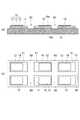
図1は、実施形態に係る半導体発光装置100を表す模式図である。半導体発光装置100は、実装面150aを有する実装基板150と、実装面150aの上に配置された半導体発光素子1と、を備える。実装面150aには、複数の配線103が設けられる。 FIG. 1 is a schematic diagram illustrating a semiconductor
半導体発光素子1は、発光層13(図2参照)を有する半導体層15を含む。そして、半導体層15に設けられたp側電極16(図2参照)と、p側電極16と複数の配線103のうちの1つを接続するp側配線部41と、を有する。また、半導体層15に設けられたn側電極17(図2参照)と、n側電極17と複数の配線103のうちの他の1つを接続するn側配線部43と、を有する。 The semiconductor
半導体層15は、発光層13の放射光を放出する第1の面15aと、第1の面15aとは反対側の第2の面15bと、を有する。p側配線部41およびn側配線部43は、第2の面側に設けられる。そして、半導体発光素子1は、第2の面側を実装面150aに向けてマウントされ、第1の面15aから発光層13の放射光を放出する。 The
半導体発光装置100は、実装面150aの上において半導体発光素子1の周りを覆う第1の樹脂(以下、樹脂層190)と、第1の樹脂層および半導体発光素子1の上に設けられた第2の樹脂(以下、樹脂層170)と、を備える。 The semiconductor
樹脂層190は、発光層13の放射光により励起されるリン光材を含む。樹脂層170は、蛍光体171を含む。蛍光体171は、発光層13から放射される光により励起され、発光層13の放射光とはピーク波長の異なる光を放射する。 The
樹脂層190に含まれるリン光材は、蛍光体171よりも長い発光時間を有する。例えば、蛍光体171の発光は、励起光が消えた後、50〜60ナノ秒(ns)で消失する。(例えば、1/eの強度となる。e:ネイピア数)一方、リン光材の発光は、蛍光体171の発光が消えた後も継続する。これにより、半導体発光装置100の経時的な発光強度の変化を抑制することができる。例えば、半導体発光装置100を交流電源を用いて駆動した場合、発光のちらつきを抑え、また、放射光の色ムラを抑制することができる。 The phosphor material included in the
また、樹脂層190に含まれるリン光材の放射光のピーク波長は、発光層13の放射光のピーク波長よりも長い。好ましくは、リン光材の放射光のピーク波長は、蛍光体171の放射光のピーク波長と同じである。ここで、リン光材の放射光のピーク波長が蛍光体171の放射光のピーク波長と同じということは、厳密な一致に限らず、蛍光体171の放射光のピーク波長に近い波長である場合も含む。 In addition, the peak wavelength of the emitted light of the phosphor included in the
次に、図2を参照して、半導体発光素子1の構造を説明する。図2は、実施形態に係る半導体発光素子1を表す模式断面図である。 Next, the structure of the semiconductor
半導体発光素子1は、発光層13を含む半導体層15を備える。半導体層15は、第1の面15aと、その反対側の第2の面15b(図9(a)参照)と、を有する。また、半導体層15は、発光層13を含む部分15eと、発光層13を含まない部分15fと、を有する。 The semiconductor
半導体層15は、第1の半導体層11と、第2の半導体層12と、発光層13と、を有する。発光層13は、第1の半導体層11と、第2の半導体層12と、の間に設けられる。第1の半導体層11および第2の半導体層12は、例えば、窒化ガリウムを含む。 The
発光層13を含む部分15eは、半導体層15のうちで、発光層13が積層されている部分である。発光層13を含まない部分15fは、半導体層15のうちで、発光層13が積層されていない部分である。 The
第1の半導体層11は、例えば、下地バッファ層、n型GaN層を含む。第2の半導体層12は、例えば、p型GaN層である。発光層13は、青、紫、青紫、紫外光などを発光する材料を含む。 The
半導体層15の第2の面15bは、凹凸形状に加工される。その凸部は、発光層13を含む部分15eであり、凹部は、発光層13を含まない部分15fである。発光層13を含む部分15eの第2の面は、第2の半導体層12の表面であり、その上にp側電極16が設けられる。発光層13を含まない部分15fの第2の面は、第1の半導体層11の表面であり、その上にn側電極17が設けられる。 The
発光層13は、p側電極16とn側電極17との間に電流を流すことにより発光する。そして、発光層13の放射光は、第1の面15aから外部に放出される。 The
例えば、半導体層15の第2の面15bにおいて、発光層13を含む部分15eの面積は、発光層13を含まない部分15fの面積よりも広く設けられる。また、発光層13を含む部分15eの上に設けられるp側電極16の面積は、発光層13を含まない部分の上に設けられるn側電極17の面積よりも広い。これにより、広い発光面が得られ、光出力を高くできる。 For example, in the
半導体層15の第2の面側には、第1の絶縁膜(以下、絶縁膜18)が設けられる。絶縁膜18は、半導体層15、p側電極16およびn側電極17を覆う。絶縁膜18は、半導体層15の第1の面15aの上には設けられない。 A first insulating film (hereinafter referred to as an insulating film 18) is provided on the second surface side of the
絶縁膜18には、例えば、シリコン酸化膜、シリコン窒化膜等の無機膜を用いる。あるいは、微細開口のパターニング性に優れたポリイミド等の樹脂を用いても良い。なお、絶縁膜18として樹脂を用いる場合、絶縁膜18と半導体層15との間に、例えば、シリコン酸化膜などの無機膜を設けても良い。無機膜は、発光層13および第2の半導体層12の側面を覆い保護する。 For the insulating
なお、本明細書において、「覆う」とは、覆うものが覆われるものに直接接する場合に限らず、他のものを介して覆う場合も含む。 In the present specification, “covering” includes not only the case where the covering is in direct contact with the covering but also the case of covering through another.
絶縁膜18の半導体層15とは反対側の面上には、p側配線層21とn側配線層22とが互いに離隔して設けられる。絶縁膜18は、p側電極16に連通した第1の開口(以下、開口18a)、および、n側電極17に連通した第2の開口(以下、開口18b)を含む。図1に示す例では、絶縁膜18は複数の開口18aを含むが、1つの開口を含む形態でも良い。 On the surface of the insulating
p側配線層21は、絶縁膜18の上、および、開口18aの内部にも設けられる。すなわち、p側配線層21は、開口18aを介してp側電極16と電気的に接続される。n側配線層22は、絶縁膜18の上、および、開口18bの内部内にも設けられ、n側電極17と電気的に接続される。 The p-
p側配線層21のp側電極16とは反対側の面上には、p側金属ピラー23が設けられる。p側配線部41は、p側配線層21およびp側金属ピラー23を含む。 A p-
n側配線層22のn側電極17とは反対側の面上には、n側金属ピラー24が設けられる。n側配線部43は、n側配線層22およびn側金属ピラー24を含む。 An n-
p側配線部41とn側配線部43との間には、第2の絶縁膜(以下、絶縁膜25)が設けられる。すなわち、絶縁膜25は、p側金属ピラー23とn側金属ピラー24との間に充填され、絶縁膜18およびp側配線部41の側面、n側配線部43の側面を覆う。 A second insulating film (hereinafter referred to as an insulating film 25) is provided between the p-
図1に表すように、絶縁膜25は、p側金属ピラー23の側面およびn側金属ピラー24の側面を覆う。一方、p側金属ピラー23のp側配線層21とは反対側の面は、絶縁膜25から露出し、p側外部端子23aとして機能する。n側金属ピラー24のn側配線層22とは反対側の面は、絶縁膜25から露出し、n側外部端子24aとして機能する。 As shown in FIG. 1, the insulating
このように、p側外部端子23aおよびn側外部端子24aは、絶縁膜25の同じ面(図1における下面)に露出する。そして、その間隔は、絶縁膜18上におけるp側配線層21とn側配線層22との間隔よりも広くすることが好ましい。すなわち、p側外部端子23aとn側外部端子24aとの間隔は、例えば、実装時のはんだの広がりよりも大きくする。これにより、p側外部端子23aおよびn側外部端子24aの間の短絡を防ぐことができる。 Thus, the p-side
これに対し、p側配線層21と、n側配線層22と、の間隔は、プロセス上の限界まで狭くすることができる。そして、p側配線層21の面積を拡大し、p側配線層21とp側金属ピラー23との接触面積を広くする。これにより、発光層13の熱放散を促進する。 On the other hand, the distance between the p-
また、複数の開口18aを通じてp側配線層21がp側電極16と接する面積は、開口18bを通じてn側配線層22がn側電極17と接する面積よりも大きくする。これにより、発光層13に流れる電流の分布を均一化できる。 The area where the p-
さらに、絶縁膜18上に設けられるn側配線層22の面積は、n側電極17の面積よりも広くすることが可能である。そして、n側配線層22の上に設けられるn側金属ピラー24の面積(すなわち、n側外部端子24aの面積)をn側電極17よりも広くできる。これにより、実装に要するn側外部端子24aの面積を維持しながら、n側電極17の面積を小さくすることが可能となる。例えば、半導体層15における発光層13を含まない部分15fの面積を縮小し、発光層13を含む部分15eの面積を拡大して光出力を向上させることが可能となる。 Furthermore, the area of the n-
第1の半導体層11は、n側電極17およびn側配線層22を介してn側金属ピラー24と電気的に接続される。第2の半導体層12は、p側電極16およびp側配線層21を介してp側金属ピラー23と電気的に接続される。 The
例えば、p側金属ピラー23はp側配線層21よりも厚く、n側金属ピラー24はn側配線層22よりも厚い。p側金属ピラー23、n側金属ピラー24および絶縁膜25の厚さは、それぞれ半導体層15よりも厚くすることができる。なお、ここで言う「厚さ」とは、図2における上下方向の各層の幅である。 For example, the p-
また、p側金属ピラー23およびn側金属ピラー24のそれぞれの厚さは、半導体層15、p側電極16、n側電極17および絶縁膜18を含む積層体の厚さよりも厚くすることができる。 In addition, the thickness of each of the p-
各金属ピラー23、24のアスペクト比(平面サイズに対する厚みの比)は任意であり、例えば、1以上であっても良いし、1より小さくても良い。すなわち、金属ピラー23、24は、その平面サイズより厚くても良いし、薄くても良い。 The aspect ratio (ratio of thickness to planar size) of each
実施形態によれば、半導体層15を形成するために使用する基板10(図8参照)が除去されても、半導体層15は、p側金属ピラー23、n側金属ピラー24および絶縁膜25により安定して支持される。このため、半導体発光素子1の機械的強度は、基板10を除去した後の処理に耐えるレベルに保持することができる。 According to the embodiment, even if the substrate 10 (see FIG. 8) used to form the
p側配線層21、n側配線層22、p側金属ピラー23およびn側金属ピラー24の材料として、例えば、銅、金、ニッケル、銀などを用いることができる。これらのうちの銅を用いると、良好な熱伝導性、高いマイグレーション耐性および絶縁材料に対する密着性を向上させることができる。 As materials for the p-
絶縁膜25は、p側金属ピラー23およびn側金属ピラー24を補強する。絶縁膜25は、実装基板と熱膨張率が同じもしくは近いものを用いるのが望ましい。そのような絶縁膜25として、例えば、エポキシ樹脂、シリコーン樹脂、フッ素樹脂などを挙げることができる。 The insulating
半導体発光素子1の実装過程では、p側外部端子23aおよびn側外部端子24aを実装基板に接続するはんだ等の部材に起因する応力が半導体層15に加わるが、p側金属ピラー23およびn側金属ピラー24は、この応力を吸収し緩和する。 In the mounting process of the semiconductor
本実施形態では、p側配線層21およびp側金属ピラー23を含むp側配線部41は、複数の開口18aの内部に設けられ相互に離隔された複数のビア21aを介して、p側電極16に接続される。例えば、複数のビア21aの接触面積を合わせた面積を有する1つのビアを介してp側配線部41をp側電極16に接続する場合よりも、半導体層15に加わる応力を低減できる。 In the present embodiment, the p-
一方、p側配線層21は、1つの大きな開口の内部に設けられビア21aよりも平面サイズの大きなポストを介してp側電極16に接続させても良い。これにより、p側電極16、p側配線層21およびp側金属ピラー23を介した放熱性の向上を図ることができる。 On the other hand, the p-
後述するように、半導体層15の形成に用いた基板10は、半導体層15から除去される。これにより、半導体発光素子1は低背化される。さらに、基板10を除去した半導体層15の第1の面15aには、微小な凹凸を形成する。例えば、第1の面15aに対して、アルカリ系溶液を使ったウェットエッチング(フロスト処理)を行い凹凸を形成する。これにより、発光層13の放射光を全反射させることなく、第1の面15aから外側に取り出すことが可能となる。 As will be described later, the
半導体発光素子1は、第1の面15aの側において、半導体層15および絶縁膜18の上に設けられ、発光層13の放射光を透過する絶縁層36をさらに備える。絶縁層36は、例えば、シリコン酸化膜またはシリコン窒化膜などの無機膜である。また、絶縁層36は、シリコーン樹脂またはエポキシ樹脂などの樹脂層であっても良い。 The semiconductor
次に、図3および図4を参照して、半導体発光装置100の製造過程を説明する。図3(a)〜図4(b)は、実施形態に係る半導体発光装置100の製造過程を表す模式断面図である。 Next, a manufacturing process of the semiconductor
まず、図3(a)に表すように、実装基板150の実装面150aの上に複数の半導体発光素子1をマウントする。実装基板150は、例えば、金属ベース101と、金属ベース101の上に設けられた絶縁層102と、絶縁層102の上に設けられた複数の配線103と、を有する。実装基板150は、配線103と、絶縁層102と、を覆うソルダーレジスト107を含む。 First, as shown in FIG. 3A, the plurality of semiconductor
半導体発光素子1は、p側配線部41およびn側配線部43を露出させた絶縁膜25の面を実装面150aに向けてマウントされる。そして、p側配線部41およびn側配線部43を、例えば、ハンダ105を介して配線103に接続する。本実施形態では、例えば、複数の半導体発光素子1が配線103を介して直列接続される。すなわち、隣り合う半導体発光素子1の間において、一方のp側配線部41が、共通する配線103を介して他方のn側配線部43に接続される。 The semiconductor
次に、図3(b)に表すように、実装基板150の上にマウントされた複数の半導体発光素子1、および、隣り合う半導体発光素子1の間の実装面150aを覆う樹脂層190を形成する。樹脂層190は、例えば、シリコーン樹脂であり、リン光材を含む。リン光材には、例えば、イリジウムなどの金属錯体を用いることができる。 Next, as illustrated in FIG. 3B, a plurality of semiconductor
次に、図4(a)に表すように、樹脂層190の半導体発光素子1の上に形成された部分を除去し、隣り合う半導体発光素子1の間に樹脂層190を残す。例えば、半導体発光素子1の上に形成された樹脂層190を研削により除去する。 Next, as illustrated in FIG. 4A, the portion of the
次に、図4(b)に表すように、半導体発光素子1および樹脂層190の上に樹脂層170を形成し、半導体発光装置100を完成する。樹脂層170は、例えば、蛍光体171が分散されたシリコーン樹脂である。発光層13が青色光を放射する場合、蛍光体171には、例えば、黄色の蛍光を放射するYAG蛍光体もしくはαサイアロン系蛍光体を用いる。また、緑色および赤色の蛍光を放射する窒化物系蛍光体を混合しても良い。 Next, as illustrated in FIG. 4B, the
図5は、実施形態に係る半導体発光装置100を表す回路図である。半導体発光装置100は、例えば、半導体発光素子1aが直列に接続された第1の発光素子群と、半導体発光素子1bが直列に接続された第2の発光素子群を含む。 FIG. 5 is a circuit diagram illustrating the semiconductor
第1の発光素子群および第2の発光素子群は、それぞれ交流電源201に並列に接続される。そして、第1の発光素子群は、交流電源201に対し、第2の発光素子群とは逆方向に接続される。すなわち、交流電源201により半導体発光装置100を駆動する場合、第1の発光素子群と第2の発光素子群は、交互に発光する。 The first light emitting element group and the second light emitting element group are each connected in parallel to the
このような駆動方式を用いた場合、例えば、第1の発光素子群が消灯され第2の発光素子群が点灯される間に輝度が低下する時間が生じる。これがちらつきや色ムラとなって視認される。本実施形態では、半導体発光素子1の輝度が低下し消灯しても、隣り合う半導体発光素子1の間に設けられた樹脂層190に含まれるリン光材の発光が継続する。これにより、半導体発光装置100では、発光のちらつきや色ムラを抑制することができる。 When such a driving method is used, for example, there is a time during which the luminance decreases while the first light emitting element group is turned off and the second light emitting element group is turned on. This is visually recognized as flickering or color unevenness. In the present embodiment, even if the brightness of the semiconductor
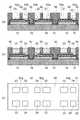
図6(a)および図6(b)は、実施形態の変形例に係る半導体発光装置200および300を表す模式断面図である。 FIG. 6A and FIG. 6B are schematic cross-sectional views showing semiconductor
図6(a)に示す半導体発光装置200は、実装基板150と、実装面150aの上に配置された半導体発光素子1と、を備える。そして、実装面150aにマウントされた半導体発光素子1の全体を覆う樹脂層190と、樹脂層190の上に設けられた樹脂層170と、をさらに備える。 A semiconductor
すなわち、樹脂層190は、半導体発光素子1の周りに設けられた部分190aと、絶縁層36の上に設けられた部分190bと、を有する。そして、樹脂層190は、発光層13の放射光により励起されるリン光材を含む。樹脂層170は、発光層13から放射される光により励起され、励起光とは波長の異なる光を放射する蛍光体171を含む。 That is, the
例えば、図4(a)に表すように絶縁層36の上に形成された樹脂層190を完全に除去する必要はなく、絶縁層36の上に薄い樹脂層190bが残っても良い。樹脂層190に含まれるリン光材の発光効率が蛍光体171の発光効率よりも低い場合には、樹脂層190bの厚さは薄いほど良い。 For example, as shown in FIG. 4A, it is not necessary to completely remove the
図6(b)に示す半導体発光装置300は、実装基板150と、実装面150aの上に配置された半導体発光素子2と、を備える。そして、半導体発光素子2の周りを覆う樹脂層190と、半導体発光素子2および樹脂層190の上に設けられた樹脂層170と、をさらに備える。 A semiconductor light emitting device 300 shown in FIG. 6B includes a mounting
半導体発光素子2は、半導体層15と、その第2の面15bの側に設けられたp側配線部41と、n側配線部43と、を備える。p側配線部41は、半導体層15の発光層13を含む部分15eの上に設けられたp側電極16に電気的に接続される。n側配線部43は、半導体層15の発光層13を含まない部分15fの上に設けられたn側電極17に電気的に接続される。 The semiconductor
さらに、半導体発光素子2は、半導体層15の第1の面15aの側に設けられた絶縁層56を有する。絶縁層56は、発光層13の放射光を散乱する散乱材57を含む。散乱材57には、例えば、シリカの微粒子を用いることができる。そして、散乱材57は、半導体層15の第1の面15aから放射される光の分布を均一化し、半導体発光素子1の配光角を広げる。これにより、半導体発光装置300の輝度分布の均一性を向上させることができる。 Further, the semiconductor
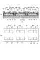
図7(a)および図7(b)は、実施形態の変形例に係る半導体発光装置400および500を模式的に表す平面図である。 FIG. 7A and FIG. 7B are plan views schematically showing semiconductor
図7(a)に表す半導体発光装置400は、実装基板150の上に千鳥状に配置された複数の半導体発光素子1を含む。すなわち、半導体発光素子1は、X方向に等間隔に並設される。そして、Y方向において、X方向の配列の位相が交互にシフトするように配置される。複数の半導体発光素子1をこのように配置することにより、発光点の並びの規則性が乱され、面光源としての発光ムラを抑制することができる。また、半導体発光素子1から横方向に放射される光の相互干渉を抑制することもできる。 A semiconductor
図7(b)に示す半導体発光装置500では、実装基板150の上に千鳥状に配置された複数の半導体発光素子2を含む。半導体発光素子2は、半導体層15の第1の面側に散乱材57を含む絶縁層56を有し、その配光角が広げられる。このため、実装基板150の上における配置間隔を広げることが可能となる。 A semiconductor
図7(b)に示す例では、X方向およびY方向における配置間隔を、それぞれの方向の半導体発光素子2のサイズよりも広くする。すなわち、隣り合う半導体発光素子2の間隔は、任意の方向において同じ方向の半導体発光素子2のサイズよりも広い。これにより、半導体発光素子1の熱を実装基板150を介して効率よく放散させることができる。 In the example shown in FIG. 7B, the arrangement interval in the X direction and the Y direction is made wider than the size of the semiconductor
次に、図8(a)〜図16(b)を参照して、実施形態に係る半導体発光素子1の製造方法について説明する。図8(a)〜図16(b)は、実施形態に係る半導体発光素子1の製造過程を表す模式図である。 Next, with reference to FIGS. 8A to 16B, a method for manufacturing the semiconductor
図8(a)は、基板10の主面上に形成された第1の半導体層11、第2の半導体層12および発光層13を表す断面図である。例えば、MOCVD(metal organic chemical vapor deposition)法を用いて、基板10の上に第1の半導体層11、発光層13および第2の半導体層12を順に成長させる。基板10は、例えば、シリコン基板である。また、基板10としてサファイア基板を用いても良い。第1の半導体層11、発光層13および第2の半導体層12は、例えば、窒化物半導体であり、窒化ガリウム(GaN)を含む。 FIG. 8A is a cross-sectional view showing the
第1の半導体層11は、例えば、n形GaN層である。また、第1の半導体層11は、基板10の上に設けられたバッファ層と、バッファ層の上に設けられたn形GaN層と、を含む積層構造を有しても良い。第2の半導体層12は、例えば、発光層13の上に設けられたp形AlGaN層と、その上に設けられたp形GaN層と、を含む。 The
図8(b)および図8(c)は、第2の半導体層12および発光層13を選択的に除去した状態を表している。図8(b)は断面図であり、図8(c)は、基板10の上面側を表す平面図である。 FIG. 8B and FIG. 8C show a state in which the
図8(b)に示すように、例えば、RIE(Reactive Ion Etching)法を用いて、第2の半導体層12および発光層13を選択的にエッチングし、第1の半導体層11を露出させる。 As shown in FIG. 8B, the
図8(c)に示すように、半導体層12および発光層13は島状にパターニングされ、基板10の上に複数の発光領域(発光層13を含む部分15e)が形成される。 As shown in FIG. 8C, the
次に、図9(a)および図9(b)に表すように、第1の半導体層11を選択的に除去し、基板10の上に複数の半導体層15を形成する。 Next, as shown in FIGS. 9A and 9B, the
図9(a)は、基板10およびその上に形成された半導体層15の断面を表している。例えば、第2の半導体層12および発光層13を覆うエッチングマスク(図示しない)を第1の半導体層11の上に設ける。続いて、RIE法を用いて第1の半導体層11をエッチングし、基板10に至る深さの溝80を形成する。 FIG. 9A shows a cross section of the
図9(b)は、半導体層15が設けられた基板10の上面を表している。溝80は、基板10の上に格子状に設けられ、第2の半導体層11を複数の半導体層15に分離する。 FIG. 9B shows the upper surface of the
半導体層15の第1の面15aは、基板10に接する面であり、第2の面15bは、第1の半導体層11および第2の半導体層12の表面である。また、溝80は、基板10の上面をエッチングし、第1の面15aよりも深い位置に設けられる。 The
溝80は、p側電極16およびn側電極17を形成した後(図10参照)に形成しても良い。 The
次に、図10(a)および図10(b)に表すように、半導体層15の第2の面15bにp側電極16とn側電極17とを形成する。図10(a)は断面図であり、図10(b)は、基板10の上面を表す平面図である。 Next, as shown in FIGS. 10A and 10B, the p-
p側電極16は、第2の半導体層12の上に形成する。n側電極17は、第1の半導体層11の上に形成する。p側電極16は、n側電極よりも広い面積を有する。 The p-
p側電極16およびn側電極17は、例えば、スパッタ法、蒸着法等で形成する。p側電極16とn側電極17は、どちらを先に形成してもよいし、同じ材料で同時に形成してもよい。p側電極16は、発光層13の放射光を反射するように形成する。例えば、p側電極16は、銀、銀合金、アルミニウム、アルミニウム合金等を含む。また、p側電極16の硫化、酸化防止のため、金属保護膜(バリアメタル)を含む構成であってもよい。また、各電極と半導体層との間のオーミックコンタクトを形成するために、熱処理を必要に応じて実施する。 The p-
次に、図11(a)に表すように、基板10の上面に絶縁膜18を形成する。図11(a)は、基板10および半導体層15の断面を表す模式図である。 Next, as illustrated in FIG. 11A, an insulating
絶縁膜18は、基板10の上に設けられた構造を覆い、第1の開口(以下、開口18a)および第2の開口(以下、18b)を有する。 The insulating
絶縁膜18は、例えば、シリコン酸化膜またはシリコン窒化膜であり、CVD(Chemical Vapor Deposition)法を用いて形成することができる。開口18aおよび18bは、例えば、レジストマスクを用いたウェットエッチングにより形成する。開口18aは、p側電極16に連通する。開口18bは、n側電極17に連通する。本実施形態では、絶縁膜18は、複数の開口18aと、1つの開口18bと、を含む。 The insulating
絶縁膜18として、例えば、ポリイミドなどの有機膜を用いても良い。また、絶縁膜18に感光性ポリイミド、ベンゾシクロブテン(Benzocyclobutene)などの有機膜を用いると、直接露光および現像ができる。このため、開口18aおよび18bのパターニングが容易になる。 For example, an organic film such as polyimide may be used as the insulating
次に、図11(b)〜図12(b)は、p側配線層21およびn側配線層22の形成過程を表している。図11(b)〜図12(a)は、基板10および半導体層15の断面を表す模式図であり、図12(a)は、基板10の上面を表す平面図である。 Next, FIG. 11B to FIG. 12B show the formation process of the p-
図11(b)に表すように、絶縁膜18の表面、第1の開口18aの内面(側壁および底面)、および第2の開口18bの内面(側壁および底面)に、金属膜19を形成する。金属膜19は、メッキ工程におけるシードメタルとして機能する。 As shown in FIG. 11B, the
金属膜19は、例えば、絶縁膜18の側から順にチタン(Ti)および銅(Cu)を含むように、スパッタ法を用いて形成する。チタンの代わりにアルミニウムを用いても良い。 For example, the
次に、図11(c)に示すように、金属膜19上にレジストマスク91を形成する。レジストマスク91は、開口91aと開口92bとを含む。開口91aは、p側電極16の上に設けられ、開口92bは、n側電極17の上に設けられる。 Next, as shown in FIG. 11C, a resist
続いて、図12(a)および図12(b)に表すように、電界銅メッキを用いてp側配線層21およびn側配線層22を形成する。すなわち、金属膜19を電流経路として、レジストマスク91の開口91aおよび91bの内部に銅(Cu)層を選択的に形成する。 Subsequently, as shown in FIGS. 12A and 12B, the p-
図12(a)に表すように、p側配線層21は、絶縁膜18の上、および、開口18aの内部にも形成される。p側配線層21は、p側電極16に電気的に接続される。n側配線層22は、絶縁膜18の上、および、開口18bの内部にも形成される。n側配線層22は、n側電極17に電気的に接続される。 As shown in FIG. 12A, the p-
図12(b)に表すように、p側配線層21とn側配線層22は、レジストマスク91gを挟んで向き合う。すなわち、p側配線層21とn側配線層22の間隔は、フォトリソグラフィの限界まで狭く設けることができる。 As shown in FIG. 12B, the p-
次に、図13(a)〜図13(c)は、p側配線層21およびn側配線層22の形成過程を表している。図13(a)および図13(b)は、基板10および半導体層15の断面を表す模式図であり、図13(c)は、基板10の上面を表す平面図である。 Next, FIGS. 13A to 13C show the formation process of the p-
図13(a)に表すように、開口92aと開口92bとを有するレジストマスク92を形成する。例えば、レジストマスク91を溶剤もしくは酸素プラズマを使って除去した後、フォトリソグラフィを用いて新たにレジストマスク91を形成する。また、レジストマスク91の上に、レジストマスク92を重ねて形成しても良い。 As shown in FIG. 13A, a resist
続いて、図13(b)に示すように、開口92aおよび92bの内部にそれぞれp側金属ピラー23およびn側金属ピラー24を形成する。p側金属ピラー23およびn側金属ピラー24は、例えば、電界Cuメッキを用いて形成する。 Subsequently, as shown in FIG. 13B, the p-
図13(c)に示すように、p側金属ピラー23とn側金属ピラー24は、レジストマスク92gを挟んで向き合う。p側金属ピラー23とn側金属ピラー24の間隔は、実装時の短絡を防ぐために、p側配線層21とn側配線層22の間隔よりも広く形成する。 As shown in FIG. 13C, the p-
図14(a)〜図14(c)は、図13(c)に続く工程を表す模式断面図である。 図14(a)に表すように、レジストマスク92を、例えば、溶剤もしくは酸素プラズマを用いて除去する。続いて、図14(b)に表すように、金属ピラー23、n側金属ピラー24、p側配線層21およびn側配線層22をマスクとして、金属膜19の露出部分をウェットエッチングにより除去する。これにより、p側配線層21とn側配線層22との間の電気的な接続が分断される。 FIG. 14A to FIG. 14C are schematic cross-sectional views showing processes subsequent to FIG. As shown in FIG. 14A, the resist
次に、図14(c)に表すように、絶縁膜18の上に第2の絶縁膜(以下、絶縁膜25)を積層する。絶縁膜25は、p側配線層21、n側配線層22、p側金属ピラー23およびn側金属ピラー24を覆う。 Next, as shown in FIG. 14C, a second insulating film (hereinafter referred to as an insulating film 25) is stacked on the insulating
絶縁膜25は、p側配線部41からn側配線部43を絶縁する。絶縁膜25は、例えば、カーボンブラックを含有し、発光層13の放射光を遮光する。また、絶縁膜25は、例えば、酸化チタンなど、発光層13の放射光を反射する部材を含有しても良い。 The insulating
次に、図15(a)〜図15(c)に示すように、半導体層15の第1の面15aの側の処理を行う。図15(a)〜図15(c)は、各工程を表す模式断面図である。 Next, as shown in FIGS. 15A to 15C, processing on the
図15(a)に示すように、半導体層15から基板10を除去する。基板10がシリコン基板の場合、例えば、ウェットエッチングにより基板10を選択的に除去することができる。基板10がサファイア基板の場合には、例えば、レーザーリフトオフ法を用いて基板10を除去する。 As shown in FIG. 15A, the
基板10の上に形成した構造体は、基板10を除去した後も絶縁膜25により支持され、ウェーハ状態を保つ。半導体層15は、p側金属ピラー23、n側金属ピラー24および絶縁膜25により支持される。これらは、半導体層15に比べて柔軟な材料であり、その応力を緩和する。例えば、基板10の上にエピタキシャル成長された半導体層は、大きな内部応力を含む。そして、その応力が基板10の剥離時に一気に開放されたとしても、p側金属ピラー23、n側金属ピラー24および絶縁膜25は、その応力を吸収する。このため、基板10を除去する過程における半導体層15の破損を回避することができる。 The structure formed on the
次に、半導体層15の第1の面15aに微細な凹凸を形成する。例えば、KOH(水酸化カリウム)水溶液やTMAH(水酸化テトラメチルアンモニウム)等で、第1の半導体層11をウェットエッチングする。このエッチングでは、結晶面方位に依存したエッチング速度の違いが生じる。このため、図15(a)に表すように、第1の面15aに凹凸を形成することができる。また、第1の面15aの上にレジストマスクを形成し、第1の半導体層11の表面を選択的にエッチングしても良い。このように、第1の面15aに凹凸を形成することにより、発光層13の放射光の取り出し効率を向上させることができる。 Next, fine irregularities are formed on the
次に、図15(b)に表すように、第1の面15aの上に絶縁層36を形成する。絶縁層36は、例えば、シリコーン樹脂またはエポキシ樹脂を含み、第1の面15aに設けられた凹凸を被覆する。 Next, as shown in FIG. 15B, an insulating
隣り合う半導体層15の間の絶縁膜18は、溝80の底面に形成された部分である。したがって、図15(b)における絶縁膜18の上面18cは、第1の面15aよりも上方に突出する。このため、絶縁層36は、絶縁膜18の上に設けられる部分が第1の面15aの上に設けられる部分よりも薄くなる。 The insulating
また、絶縁層36は、例えば、シリコン酸化膜またはシリコン窒化膜などの無機膜であっても良い。 The insulating
続いて、半導体層15の第2の面15bの側において、絶縁膜25の表面を研削し、p側金属ピラー23およびn側金属ピラー24を露出させる。p側金属ピラー23の露出面は、p側外部端子23aであり、n側金属ピラー24の露出面は、n側外部端子24aである。 Subsequently, the surface of the insulating
次に、図16(a)および図16(b)に示すように、隣り合う半導体層15の間において、絶縁層36、絶縁膜18および絶縁膜25を切断する。これにより、半導体層15を含む半導体発光素子1を個片化する。図16(a)は、半導体発光素子1の断面を表し、図16(b)は、p側外部端子23aおよびn側外部端子24aが露出した絶縁膜25の表面を表している。 Next, as shown in FIGS. 16A and 16B, the insulating
絶縁層36、絶縁膜18および絶縁膜25の切断は、例えば、ダイシングブレードを用いて行う。また、レーザ照射により切断しても良い。 The insulating
半導体層15は、溝80に存在しないためダイシングによるダメージを受けることがない。また、個片化された時点で、半導体層15の端部(側面)が絶縁膜18で覆われ保護された構造が得られる。 Since the
ダイシングする前の工程は、ウェーハ状態で一括して行われるため、個片化された個々のデバイスごとに、配線およびパッケージングを行う必要がなく、大幅なコストの低減が可能になる。すなわち、個片化された状態で、すでに配線およびパッケージングが施されている。このため、本実施形態によれば、生産性を高めることが可能であり、製造コストを低減できる。 Since the process before dicing is performed collectively in a wafer state, it is not necessary to perform wiring and packaging for each individual device, and the cost can be greatly reduced. That is, wiring and packaging have already been performed in the state of being separated. For this reason, according to this embodiment, productivity can be improved and manufacturing cost can be reduced.
上記の実施形態では、実装基板150の上に半導体発光素子1を配置する例を示したが、これに限定される訳ではない。例えば、p側電極およびn側電極を実装面とは反対側に有する半導体発光素子でも良い。また、p側電極およびn側電極が半導体層の第1の面側および第2の面側にそれぞれ設けられた縦型構造を有する半導体発光素子であっても良い。 In the above embodiment, the example in which the semiconductor
本発明のいくつかの実施形態を説明したが、これらの実施形態は、例として提示したものであり、発明の範囲を限定することは意図していない。これら新規な実施形態は、その他の様々な形態で実施されることが可能であり、発明の要旨を逸脱しない範囲で、種々の省略、置き換え、変更を行うことができる。これら実施形態やその変形は、発明の範囲や要旨に含まれるとともに、特許請求の範囲に記載された発明とその均等の範囲に含まれる。 Although several embodiments of the present invention have been described, these embodiments are presented by way of example and are not intended to limit the scope of the invention. These novel embodiments can be implemented in various other forms, and various omissions, replacements, and changes can be made without departing from the scope of the invention. These embodiments and modifications thereof are included in the scope and gist of the invention, and are included in the invention described in the claims and the equivalents thereof.
1、1a、1b、2・・・半導体発光素子、 10・・・基板、 11・・・第1の半導体層、 12・・・第2の半導体層、 13・・・発光層、 15・・・半導体層、 15a・・・第1の面、 15b・・・第2の面、 16・・・p側電極、 17・・・n側電極、 18、25・・・絶縁膜、 18a、18b、91a、91b、92a、92b・・・開口、 18c・・・上面、 19・・・金属膜、 21・・・p側配線層、 21a・・・ビア、 22・・・n側配線層、 23・・・p側金属ピラー、 23a・・・p側外部端子、 24・・・n側金属ピラー、 24a・・・n側外部端子、 36、56・・・絶縁層、 41・・・p側配線部、 43・・・n側配線部、 57・・・散乱材、 80・・・溝、 91、91g、92、92g・・・レジストマスク、 100、200、300、400、500・・・半導体発光装置、 101・・・金属ベース、 102・・・絶縁層、 103・・・配線、 105・・・ハンダ、 107・・・ソルダーレジスト、 150・・・実装基板、 150a・・・実装面、 170・・・樹脂層、 171・・・蛍光体、 190・・・樹脂層、 201・・・交流電源 DESCRIPTION OF
Claims (9)
Translated fromJapanese前記実装面上に配置された半導体発光素子であって、
発光層を有する半導体層と、
前記半導体層に接続されたp側電極と、
前記p側電極と前記複数の配線のうちの1つとを接続するp側配線部と、
前記半導体層に接続されたn側電極と、
前記n側電極と前記複数の配線のうちの他の1つとを接続するn側配線部と、
前記p側配線部と前記n側配線部との間に設けられ、前記p側配線部の側面および前記n側配線部の側面に接する絶縁膜と、
を有する半導体発光素子と、
前記実装面上において前記半導体発光素子の周りを覆い、前記発光層の放射光により励起されるリン光材を含む第1の樹脂と、
前記第1の樹脂および前記半導体発光素子の上に設けられた第2の樹脂であって、前記発光層の放射光により励起され、前記発光層の放射光とはピーク波長が異なる光を放射する蛍光体を含む第2の樹脂と、
を備え、
前記p側配線部は、前記p側電極に電気的に接続されたp側配線層と、前記複数の配線のうちの1つに接続されたp側金属ピラーと、を含み、
前記n側配線部は、前記n側電極に電気的に接続されたn側配線層と、前記複数の配線のうちの他の1つに接続されたn側金属ピラーと、を含む半導体発光装置。A mounting substrate having a mounting surface provided with a plurality of wirings;
A semiconductor light emitting device disposed on the mounting surface,
A semiconductor layer having a light emitting layer;
A p-side electrode connected to the semiconductor layer;
A p-side wiring portion connecting the p-side electrode and one of the plurality of wirings;
An n-side electrode connected to the semiconductor layer;
An n-side wiring portion connecting the n-side electrode and the other one of the plurality of wirings;
An insulating film provided between the p-side wiring portion and the n-side wiring portion and in contact with a side surface of the p-side wiring portion and a side surface of the n-side wiring portion;
A semiconductor light emitting device having:
A first resin including a phosphorescent material that covers the semiconductor light emitting element on the mounting surface and is excited by the emitted light of the light emitting layer;
A second resin provided on the first resin and the semiconductor light emitting element, which is excited by the light emitted from the light emitting layer and emits light having a peak wavelength different from that of the light emitted from the light emitting layer. A second resin containing a phosphor;
With
The p-side wiring portion includes a p-side wiring layer electrically connected to the p-side electrode, and a p-side metal pillar connected to one of the plurality of wirings,
The n-side wiring portion includes an n-side wiring layer electrically connected to the n-side electrode, and an n-side metal pillar connected to another one of the plurality of wirings. .
前記実装面上に配置された半導体発光素子であって、
発光層を有する半導体層と、
前記半導体層に接続されたp側電極と、
前記p側電極と前記複数の配線のうちの1つとを接続するp側配線部と、
前記半導体層に接続されたn側電極と、
前記n側電極と前記複数の配線のうちの他の1つとを接続するn側配線部と、
を有する半導体発光素子と、
前記実装面上において前記半導体発光素子の周りを覆い、前記発光層の放射光により励起されるリン光材を含む第1の樹脂と、
前記第1の樹脂および前記半導体発光素子の上に設けられた第2の樹脂であって、前記発光層の放射光により励起され、前記発光層の放射光とはピーク波長が異なる光を放射する蛍光体を含む第2の樹脂と、
を備えた半導体発光装置。A mounting substrate having a mounting surface provided with a plurality of wirings;
A semiconductor light emitting device disposed on the mounting surface,
A semiconductor layer having a light emitting layer;
A p-side electrode connected to the semiconductor layer;
A p-side wiring portion connecting the p-side electrode and one of the plurality of wirings;
An n-side electrode connected to the semiconductor layer;
An n-side wiring portion connecting the n-side electrode and the other one of the plurality of wirings;
A semiconductor light emitting device having:
A first resin including a phosphorescent material that covers the semiconductor light emitting element on the mounting surface and is excited by the emitted light of the light emitting layer;
A second resin provided on the first resin and the semiconductor light emitting element, which is excited by the light emitted from the light emitting layer and emits light having a peak wavelength different from that of the light emitted from the light emitting layer. A second resin containing a phosphor;
A semiconductor light emitting device comprising:
前記p側配線部および前記n側配線部は、前記第2の面側に設けられ、
前記半導体素子は、前記第2の面を前記実装面に向けてマウントされた請求項2〜6のいずれか1つに記載の半導体発光装置。The semiconductor layer has a first surface that emits radiated light of the light emitting layer, and a second surface opposite to the first surface;
The p-side wiring portion and the n-side wiring portion are provided on the second surface side,
The semiconductor light-emitting device according to claim 2, wherein the semiconductor element is mounted with the second surface facing the mounting surface.
前記発光層の放射光を透過する層は、前記発光層の放射光を散乱する散乱材を含む請求項7または8に記載の半導体発光装置。The semiconductor light emitting element has a layer provided on the first surface and transmitting the emitted light of the light emitting layer,
The semiconductor light-emitting device according to claim 7, wherein the layer that transmits the emitted light of the light-emitting layer includes a scattering material that scatters the emitted light of the light-emitting layer.
Priority Applications (4)
| Application Number | Priority Date | Filing Date | Title |
|---|---|---|---|
| JP2013008809AJP2014139999A (en) | 2013-01-21 | 2013-01-21 | Semiconductor light-emitting device |
| TW102108629ATWI499096B (en) | 2013-01-21 | 2013-03-12 | Semiconductor light emitting device |
| EP13160133.8AEP2757602A2 (en) | 2013-01-21 | 2013-03-20 | Semiconductor light emitting device |
| US13/847,643US8937331B2 (en) | 2013-01-21 | 2013-03-20 | Semiconductor light emitting device |
Applications Claiming Priority (1)
| Application Number | Priority Date | Filing Date | Title |
|---|---|---|---|
| JP2013008809AJP2014139999A (en) | 2013-01-21 | 2013-01-21 | Semiconductor light-emitting device |
Publications (1)
| Publication Number | Publication Date |
|---|---|
| JP2014139999Atrue JP2014139999A (en) | 2014-07-31 |
Family
ID=47891545
Family Applications (1)
| Application Number | Title | Priority Date | Filing Date |
|---|---|---|---|
| JP2013008809APendingJP2014139999A (en) | 2013-01-21 | 2013-01-21 | Semiconductor light-emitting device |
Country Status (4)
| Country | Link |
|---|---|
| US (1) | US8937331B2 (en) |
| EP (1) | EP2757602A2 (en) |
| JP (1) | JP2014139999A (en) |
| TW (1) | TWI499096B (en) |
Cited By (4)
| Publication number | Priority date | Publication date | Assignee | Title |
|---|---|---|---|---|
| JP2017055006A (en)* | 2015-09-11 | 2017-03-16 | 株式会社東芝 | Light emitting device |
| JP2018110253A (en)* | 2018-02-19 | 2018-07-12 | アルパッド株式会社 | Light emitting unit and semiconductor light emitting device |
| JP2019012816A (en)* | 2017-06-30 | 2019-01-24 | 日亜化学工業株式会社 | Light-emitting device and manufacturing method thereof |
| JP2019096902A (en)* | 2015-01-30 | 2019-06-20 | オスラム オプト セミコンダクターズ ゲゼルシャフト ミット ベシュレンクテル ハフツングOsram Opto Semiconductors GmbH | Method for manufacturing semiconductor component and semiconductor component |
Families Citing this family (3)
| Publication number | Priority date | Publication date | Assignee | Title |
|---|---|---|---|---|
| CN104779339B (en)* | 2015-01-15 | 2017-08-25 | 大连德豪光电科技有限公司 | Upside-down mounting high voltage LED chip and preparation method thereof |
| US10756008B2 (en)* | 2016-03-25 | 2020-08-25 | Hitachi Chemical Company, Ltd. | Organic interposer and method for manufacturing organic interposer |
| CN106384733A (en)* | 2016-10-31 | 2017-02-08 | 广东晶科电子股份有限公司 | 360-degree light-transmitting LED filament and preparation method thereof |
Citations (4)
| Publication number | Priority date | Publication date | Assignee | Title |
|---|---|---|---|---|
| JP2010062274A (en)* | 2008-09-03 | 2010-03-18 | Toshiba Corp | Semiconductor light-emitting element and its manufacturing method |
| JP2011529621A (en)* | 2008-07-29 | 2011-12-08 | ソウル セミコンダクター カンパニー リミテッド | Warm white light emitting device and backlight module including the same |
| JP2012099605A (en)* | 2010-11-01 | 2012-05-24 | Citizen Electronics Co Ltd | Semiconductor light-emitting device |
| JP2012195345A (en)* | 2011-03-15 | 2012-10-11 | Toshiba Corp | Semiconductor light-emitting device |
Family Cites Families (12)
| Publication number | Priority date | Publication date | Assignee | Title |
|---|---|---|---|---|
| CA2489237A1 (en) | 2002-06-13 | 2003-12-24 | Cree, Inc. | Semiconductor emitter comprising a saturated phosphor |
| KR20050113200A (en) | 2003-02-26 | 2005-12-01 | 크리, 인코포레이티드 | Composite white light source and method for fabricating |
| US9159888B2 (en) | 2007-01-22 | 2015-10-13 | Cree, Inc. | Wafer level phosphor coating method and devices fabricated utilizing method |
| US8680550B2 (en)* | 2008-07-03 | 2014-03-25 | Samsung Electronics Co., Ltd. | Wavelength-converting light emitting diode (LED) chip and LED device equipped with chip |
| JP4724222B2 (en) | 2008-12-12 | 2011-07-13 | 株式会社東芝 | Method for manufacturing light emitting device |
| JP5050045B2 (en)* | 2009-12-22 | 2012-10-17 | 株式会社東芝 | Light emitting device |
| JP5101650B2 (en)* | 2010-03-25 | 2012-12-19 | 株式会社東芝 | Semiconductor light emitting device and manufacturing method thereof |
| JP2011253925A (en)* | 2010-06-02 | 2011-12-15 | Toshiba Corp | Method of manufacturing light-emitting device |
| TW201145614A (en) | 2010-06-03 | 2011-12-16 | Toshiba Kk | Method for manufacturing light-emitting device and light-emitting device manufactured by the same |
| JP4875185B2 (en)* | 2010-06-07 | 2012-02-15 | 株式会社東芝 | Optical semiconductor device |
| JP5759790B2 (en) | 2010-06-07 | 2015-08-05 | 株式会社東芝 | Manufacturing method of semiconductor light emitting device |
| KR101832536B1 (en)* | 2010-08-31 | 2018-02-26 | 니치아 카가쿠 고교 가부시키가이샤 | Light emitting device and method for manufacturing same |
- 2013
- 2013-01-21JPJP2013008809Apatent/JP2014139999A/enactivePending
- 2013-03-12TWTW102108629Apatent/TWI499096B/ennot_activeIP Right Cessation
- 2013-03-20EPEP13160133.8Apatent/EP2757602A2/ennot_activeWithdrawn
- 2013-03-20USUS13/847,643patent/US8937331B2/ennot_activeExpired - Fee Related
Patent Citations (4)
| Publication number | Priority date | Publication date | Assignee | Title |
|---|---|---|---|---|
| JP2011529621A (en)* | 2008-07-29 | 2011-12-08 | ソウル セミコンダクター カンパニー リミテッド | Warm white light emitting device and backlight module including the same |
| JP2010062274A (en)* | 2008-09-03 | 2010-03-18 | Toshiba Corp | Semiconductor light-emitting element and its manufacturing method |
| JP2012099605A (en)* | 2010-11-01 | 2012-05-24 | Citizen Electronics Co Ltd | Semiconductor light-emitting device |
| JP2012195345A (en)* | 2011-03-15 | 2012-10-11 | Toshiba Corp | Semiconductor light-emitting device |
Cited By (4)
| Publication number | Priority date | Publication date | Assignee | Title |
|---|---|---|---|---|
| JP2019096902A (en)* | 2015-01-30 | 2019-06-20 | オスラム オプト セミコンダクターズ ゲゼルシャフト ミット ベシュレンクテル ハフツングOsram Opto Semiconductors GmbH | Method for manufacturing semiconductor component and semiconductor component |
| JP2017055006A (en)* | 2015-09-11 | 2017-03-16 | 株式会社東芝 | Light emitting device |
| JP2019012816A (en)* | 2017-06-30 | 2019-01-24 | 日亜化学工業株式会社 | Light-emitting device and manufacturing method thereof |
| JP2018110253A (en)* | 2018-02-19 | 2018-07-12 | アルパッド株式会社 | Light emitting unit and semiconductor light emitting device |
Also Published As
| Publication number | Publication date |
|---|---|
| TWI499096B (en) | 2015-09-01 |
| EP2757602A2 (en) | 2014-07-23 |
| US8937331B2 (en) | 2015-01-20 |
| US20140203313A1 (en) | 2014-07-24 |
| TW201431134A (en) | 2014-08-01 |
Similar Documents
| Publication | Publication Date | Title |
|---|---|---|
| JP5816127B2 (en) | Semiconductor light emitting device and manufacturing method thereof | |
| US9006764B2 (en) | Semiconductor light emitting device and light emitting device | |
| JP5356312B2 (en) | Semiconductor light emitting device | |
| TWI429108B (en) | Semiconductor light emitting device | |
| JP5414579B2 (en) | Semiconductor light emitting device | |
| JP5710532B2 (en) | Semiconductor light emitting device and manufacturing method thereof | |
| JP6074317B2 (en) | Semiconductor light emitting device and light source unit | |
| TWI514631B (en) | Semiconductor light emitting device and manufacturing method thereof | |
| JP5855194B2 (en) | Semiconductor light emitting device and manufacturing method thereof | |
| JP2013065726A (en) | Semiconductor light-emitting device and method of manufacturing the same | |
| JP2014139999A (en) | Semiconductor light-emitting device | |
| JP5837456B2 (en) | Semiconductor light emitting device and light emitting module | |
| TW201434181A (en) | Semiconductor light emitting device and method of manufacturing same | |
| JP2016001750A (en) | Semiconductor light emitting device | |
| JP2015176963A (en) | Semiconductor light emitting device | |
| JP2014157991A (en) | Semiconductor light-emitting device and method of manufacturing the same | |
| TWI505499B (en) | Semiconductor light emitting device | |
| HK1198073A (en) | Semiconductor light emitting device | |
| HK1190827A (en) | Semiconductor light emitting device and light emitting module |
Legal Events
| Date | Code | Title | Description |
|---|---|---|---|
| A621 | Written request for application examination | Free format text:JAPANESE INTERMEDIATE CODE: A621 Effective date:20150204 | |
| A977 | Report on retrieval | Free format text:JAPANESE INTERMEDIATE CODE: A971007 Effective date:20151118 | |
| A131 | Notification of reasons for refusal | Free format text:JAPANESE INTERMEDIATE CODE: A131 Effective date:20151130 | |
| A02 | Decision of refusal | Free format text:JAPANESE INTERMEDIATE CODE: A02 Effective date:20160329 |