JP2014138423A - Switching device with resistive divider - Google Patents
Switching device with resistive dividerDownload PDFInfo
- Publication number
- JP2014138423A JP2014138423AJP2014003422AJP2014003422AJP2014138423AJP 2014138423 AJP2014138423 AJP 2014138423AJP 2014003422 AJP2014003422 AJP 2014003422AJP 2014003422 AJP2014003422 AJP 2014003422AJP 2014138423 AJP2014138423 AJP 2014138423A
- Authority
- JP
- Japan
- Prior art keywords
- voltage
- terminal
- resistor
- gate
- fet
- Prior art date
- Legal status (The legal status is an assumption and is not a legal conclusion. Google has not performed a legal analysis and makes no representation as to the accuracy of the status listed.)
- Granted
Links
Images


Classifications
- H—ELECTRICITY
- H01—ELECTRIC ELEMENTS
- H01L—SEMICONDUCTOR DEVICES NOT COVERED BY CLASS H10
- H01L24/00—Arrangements for connecting or disconnecting semiconductor or solid-state bodies; Methods or apparatus related thereto
- H—ELECTRICITY
- H10—SEMICONDUCTOR DEVICES; ELECTRIC SOLID-STATE DEVICES NOT OTHERWISE PROVIDED FOR
- H10D—INORGANIC ELECTRIC SEMICONDUCTOR DEVICES
- H10D84/00—Integrated devices formed in or on semiconductor substrates that comprise only semiconducting layers, e.g. on Si wafers or on GaAs-on-Si wafers
- H10D84/80—Integrated devices formed in or on semiconductor substrates that comprise only semiconducting layers, e.g. on Si wafers or on GaAs-on-Si wafers characterised by the integration of at least one component covered by groups H10D12/00 or H10D30/00, e.g. integration of IGFETs
- H10D84/811—Combinations of field-effect devices and one or more diodes, capacitors or resistors
- H—ELECTRICITY
- H01—ELECTRIC ELEMENTS
- H01L—SEMICONDUCTOR DEVICES NOT COVERED BY CLASS H10
- H01L2924/00—Indexing scheme for arrangements or methods for connecting or disconnecting semiconductor or solid-state bodies as covered by H01L24/00
- H01L2924/10—Details of semiconductor or other solid state devices to be connected
- H01L2924/11—Device type
- H01L2924/13—Discrete devices, e.g. 3 terminal devices
- H01L2924/1304—Transistor
- H01L2924/1306—Field-effect transistor [FET]
- H01L2924/13091—Metal-Oxide-Semiconductor Field-Effect Transistor [MOSFET]
Landscapes
- Engineering & Computer Science (AREA)
- Computer Hardware Design (AREA)
- Microelectronics & Electronic Packaging (AREA)
- Power Engineering (AREA)
- Electronic Switches (AREA)
- Physics & Mathematics (AREA)
- Electromagnetism (AREA)
- General Physics & Mathematics (AREA)
- Radar, Positioning & Navigation (AREA)
- Automation & Control Theory (AREA)
- Semiconductor Integrated Circuits (AREA)
- Power Conversion In General (AREA)
Abstract
Translated fromJapaneseDescription
Translated fromJapanese本開示の実施の形態は、一般に回路分野に関し、特に、電界効果トランジスタ(FET)を用いたスイッチ装置に関する。 Embodiments of the present disclosure generally relate to the circuit field, and more particularly, to a switch device using a field effect transistor (FET).
無線周波数(RF)スイッチ装置は、多用途に用いられており、例えば、RF信号を選択的に通過させるための無線周波数システムに用いられる。FETを含むスイッチ装置において、FETをオン状態にバイアスするために、ゲート端子へのバイアス電圧の印加が必要とされうる。いくつかのケースにおいて、この印加電圧は、FETのボディを不定の電圧に浮遊(float)させることとなりうる。 Radio frequency (RF) switch devices are used in many applications, for example, in radio frequency systems for selectively passing RF signals. In a switch device that includes an FET, it may be necessary to apply a bias voltage to the gate terminal in order to bias the FET to an on state. In some cases, this applied voltage can cause the FET body to float to an indeterminate voltage.
実施の形態は、例示を目的とし、添付の図面の記載に限定されないことを目的として例示される。添付の図面において同種の要素には同種の符号が付される。 The embodiments are illustrated for purposes of illustration and not limitation to the description of the accompanying drawings. In the accompanying drawings, the same kind of elements are denoted by the same reference numerals.
例示される実施の形態に係る様々な態様は、当業者にとって一般的に採用される用語を用いて他の当業者に本発明の本質を伝えるために示される。しかしながら、以下に示されるいくつかの要素のみを用いて代替的な実施の形態を実施しうることは、当業者にとって明らかであろう。説明のために、特定の装置または構成は、例示される実施の形態の詳細な理解を与えるために示される。しかし、当業者にとって、代替的な実施の形態を具体的な細部を省いて実施しうることは明らかであろう。他の例では、例示される実施の形態を不明確としないために、周知な特徴は除外され、もしくは単純化される。 Various aspects of the illustrated embodiments are set forth to convey the essence of the invention to others skilled in the art using terms commonly employed by those skilled in the art. However, it will be apparent to those skilled in the art that alternative embodiments may be practiced using only some of the elements shown below. For purposes of explanation, specific devices or configurations are set forth in order to provide a thorough understanding of the illustrated embodiments. However, it will be apparent to one skilled in the art that alternative embodiments may be practiced without the specific details. In other instances, well-known features are omitted or simplified in order not to obscure the illustrated embodiments.
さらに、様々な動作は、複数の個別の動作として本開示の理解を最も助ける形で順に示される。しかしながら、記載の順序は、これらの動作が必ずしも順序依存であることを示すものであるとして解釈されるべきはない。特に、これらの動作は、説明される順序で実行される必要はない。 Further, the various operations are shown in sequence as a plurality of individual operations in a manner that best assists in understanding the present disclosure. However, the order of description should not be construed as indicating that these operations are necessarily order dependent. In particular, these operations need not be performed in the order described.
「一つの実施の形態において」の語は、繰り返し用いられる。この語は、ほとんどの場合において、同じ実施の形態を参照するものではないが、同じ実施の形態を参照するかもしれない。「備える」、「有する」および「含む」の語は、文脈において別に規定されない限り、同義語である。 The term “in one embodiment” is used repeatedly. This term is in most cases not referring to the same embodiment, but may refer to the same embodiment. The terms “comprising”, “having” and “including” are synonymous unless the context clearly dictates otherwise.
種々の実施の形態の結合に用いうる用語に対し、文脈上の明確性を与えるため、「A/B」および「Aおよび/またはB」の語は、(A)、(B)または(AおよびB)を意味することとする。また、「A、Bおよび/またはC」の語は、(A)、(B)、(C)、(AおよびB)、(AおよびC)、(BおよびC)または(A、BおよびC)を意味する。 In order to give contextual clarity to terms that may be used to combine various embodiments, the terms “A / B” and “A and / or B” are referred to as (A), (B) or (A And B). Also, the term “A, B and / or C” means (A), (B), (C), (A and B), (A and C), (B and C) or (A, B and C).
「〜と接続される」の語は、ここでは、派生的に用いられうる。「接続される」は、以下に示す一以上の意味で用いられうる。「接続される」は、二以上の要素が物理的または電気的に直接接触することを意味しうる。しかしながら、「接続される」は、二以上の要素が互いに間接的に接触しつつ互いに協働または相互作用することも意味し、また、一つ以上の他の要素が、上述の意味で互いに接続された要素間において結合または接続されることを意味しうる。 The term “connected with” may be used herein derivatively. “Connected” can be used in one or more of the following ways. “Connected” may mean that two or more elements are in direct physical or electrical contact. However, “connected” also means that two or more elements cooperate or interact with each other while indirectly contacting each other, and one or more other elements are connected to each other in the sense described above. It may mean coupled or connected between connected elements.
実施の形態は、スイッチ装置またはFETを含むスイッチ回路を含んでもよい。FETは、ボディ、ソース、ドレインおよびゲートを備えてもよい。回路は、FETに接続される抵抗分圧器を含んでもよい。実施の形態において、抵抗分圧器は、電気的にFETのボディとグランドの間に位置し、FETに電気的に接続される第1抵抗を備えてもよい。抵抗分圧器は、電気的にFETのボディとゲートの間に位置し、FETに電気的に接続される第2抵抗をさらに備えてもよい。いくつかの実施の形態において、複数のFETおよび複数の抵抗分圧器は、スイッチ装置またはスイッチ回路に用いられてもよい。 Embodiments may include switch devices or switch circuits including FETs. The FET may comprise a body, a source, a drain and a gate. The circuit may include a resistive voltage divider connected to the FET. In an embodiment, the resistive voltage divider may include a first resistor that is electrically located between the FET body and ground and electrically connected to the FET. The resistor voltage divider may further include a second resistor that is electrically located between the FET body and the gate and is electrically connected to the FET. In some embodiments, multiple FETs and multiple resistive voltage dividers may be used in a switch device or switch circuit.
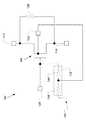
図1は、種々の実施の形態に係るスイッチ回路100を示す。スイッチ回路100(以下、回路100ともいう)は、電界効果トランジスタ(FET)を含んでもよい。FET104は、後述する図2に示されるFETのドレイン、ソース、ゲートおよびボディのそれぞれに接続される、ドレイン端子112、ソース端子116、ゲート端子120およびボディ端子124を含んでもよい。いくつかの実施の形態において、ドレイン端子112およびソース端子116は、図1に示されるように、電気的に互いに接続されてもよい。いくつかの実施の形態において、ドレイン端子112およびソース端子116の間の電気的な接続には、抵抗128が含まれてもよい。いくつかの実施の形態において、FET104は、エンハンスモードのFETであってもよい。追加的または代替的に、FET104は、シリコン−オン−インシュレータ(SOI)および/またはバルク相補的金属酸化膜半導体(CMOS)装置であってもよい。いくつかの実施の形態において、FET104は、金属酸化膜半導体(MOSFET)であってもよいが、他の実施の形態において、FET104は、絶縁ゲートFET(IFFET)や金属絶縁体半導体(MISFET)としてもよい。 FIG. 1 shows a
種々の実施の形態は、FET104のボディの電圧にバイアスをかけるために用いられるバイアス構造を提供する。このバイアス構造は、ここでは、n型のエンハンスメントモードFETに関して説明する。しかしながら、他の実施の形態において、このバイアス構造は、p型FETのような他の種類のFET向けの用途として、使用および/または変更(modify)されうる。 Various embodiments provide a bias structure that is used to bias the voltage on the body of the
種々の実施の形態において、FET104は、後に無線周波数(RF)信号として示される伝送信号の切り替えを実現するため、「オフ」状態と「オン」状態の間で選択的に遷移しうる。例えば、FET104は、FET104が「オン」状態の場合、RF信号をソース端子116で受信し、FET104を通ってドレイン端子112へRF信号を通過させてもよい。FET104は、FET104が「オフ」状態の場合、ドレイン端子112とソース端子116の間のRF信号の通過を妨げてもよい。 In various embodiments, the
FET104は、FET104を「オフ」状態と「オン」状態との間で遷移させるため、ゲート端子120において制御信号を受信してもよい。例えば、ドレイン端子112およびソース端子116の電圧に対応する、+2.5Vの直流電圧がゲート端子120に印加されてもよい。いくつかの実施の形態において、この電圧は、デコーダ(図1に不図示)により印加されてもよい。この+2.5Vの電圧は、ドレイン端子112とソース端子116の間の抵抗を極めて小さくし、その結果、RF信号がドレイン端子112およびソース端子116の間を通過できるようにすることで、FET104を「オン」にする効果を有してもよい。 The
正の電圧をゲート端子120に印加することで、RF信号がFET104を通過できるようにしうる。FET104は、図2にNMOS−FETとして示されるように、4つの要素を一般に備えてもためである。FET104は、ドレイン端子112に接続されるドレイン200と、ソース端子116に接続されるソース204と、ゲート端子120に接続されるゲート208により構成されてもよい。実施の形態において、ドレイン200、ソース204およびゲート208は、例えば、アルミニウムまたは銅などの金属または導電性材料で構成されてもよい。実施の形態において、ドレイン200、ソース204およびゲート208は、同じ材料または異なる材料で構成されてもよい。 Applying a positive voltage to the
FET104は、さらに、ボディ端子124に接続されるボディ212を備えてもよい。FET104は、詳細を後述するように、ドレイン200およびボディ212の間に位置するn型のドレイン部220と、ソース204およびボディ212の間に位置するn型のソース部228をさらに備えてもよい。 The
ここで、「端子」は、一般に、FET104を構成する要素であって、FET104が回路内の別の要素と接続する接続箇所として示される。いくつかの実施の形態において、ドレイン200およびドレイン端子112は、同じ要素であると考えてもよく、例えば、FET104は、ドレイン200と回路内の要素との直接接続を通じて、回路内の別の要素と接続してもよい。他の実施の形態においては、ドレイン端子112は、例えば、導電性のリード線など、電気的にドレイン200に接続される端子であってもよい。例えば、これらの他の実施の形態において、FET104は、ドレイン端子112を通じて回路内の別の要素と接続してもよく、このときのドレイン端子112は、ドレイン200に接続される、銅などの金属のリード線や他の導電性のリード線であってもよい。同様に、ソース204およびソース端子116は、ドレイン200およびドレイン端子112に関して上述したように、互いに同一であってもよいし、または、互いに電気的に接続されてもよい。同様に、ゲート208およびゲート端子120は、互いに同一であってもよいし、または、互いに電気的に接続されてもよい。最後に、ボディ212およびボディ端子124は、互いに同一であってもよいし、または、互いに接続されていてもよい。いくつかの実施の形態において、ボディ端子124は、ソース端子116に直接接続されてもよい。ここで、各要素に与えられる名称は、FET104の一つの要素を別の要素から識別するためのものであり、異なる実施の形態では異なる名称を用いるかもしれない。例えば、FET104において、n型のドレイン部220を「ドレイン」と呼び、n型のソース部228を「ソース」と呼ぶかもしれない。 Here, the “terminal” is generally an element that constitutes the
FET104を用いる例として、直流電圧は、ゲート端子120に印加されるものとして説明され、同時に、ゲート端子120によりゲート208が特定の電圧を得ることとなりうるであろう。しかしながら、いくつかの実施の形態において、この直流電圧は、ゲート208に直接印加されてもよい。他の例として、RF信号は、FET104が「オン」のときに、ソース204またはソース端子116のいずれかにおいて受信され、FET104を通って、ドレイン200またはドレイン端子112へ通過してもよい。 As an example using the
ボディ212は、p型材料、例えば、シリコンやゲルマニウムなどのIV族元素に、ホウ素やアルミニウムなどのIII族元素をドープしたもので構成されてもよい。n型のドレイン部220およびソース部228は、シリコンやゲルマニウムなどのIV族元素に、ヒ素やリンなどのV属元素をドープしたもので構成されてもよい。n型のドレイン部220およびソース部228は、ボディ212により互いに分離されてもよい。一般に、p型材料は、電子が欠乏し、「電子ホール」を有すると言われる。n型材料は、n型材料の内外にて電流として移動することのできうる余分な電子を有し、その結果、「可動電子」を有するといわれる。 The
上述したように、FET104のゲート208は、銅やアルミニウムなどの導電性の金属で構成されてもよい。他の実施の形態において、ゲート208は、タンタル、タングステン、窒化タンタルより構成されてもよい。他の実施の形態において、FET104のゲート208は、ポリシリコン材料で構成されてもよい。ドレイン200、ソース204、ゲート208およびボディ212は全て、誘電体224により互いに分離されてもよい。誘電体224は、例えば、二酸化シリコン、酸化窒化シリコン、または、ドレイン200とソース204の間の電子の流れを妨げる、その他の高誘電率(High-k)の誘電材料などである。 As described above, the
ゲート端子120に正電圧が印加されることによりゲート208が正の電圧を得るとき、ゲート208とFET104の他の部分との間に静電界が形成されてもよい。この正電圧は、ボディ212を構成するp型材料中の電子ホールを遠ざける一方で、ボディ212を構成するp型材料中の自由電子を引きつけうる。同時に、この正のゲート電圧は、n型のドレイン部220およびソース部228中の可動電子を引きつけうる。「閾値電圧」として知られる、ドレイン200およびソース204の直流電圧と比べてゲート208の正電圧が十分に高くなると、ボディ212を構成するp型材料における反発作用、および、ボディ212中の自由電子とn型のドレイン部220およびソース部228中の可動電子への誘引作用により、電子チャネルが形成されうる。この電子チャネルは、しばしば、「反転層」と呼ばれ、n型のドレイン部220およびソース部228の間であって誘電体224の直下に存在しうる。言い換えれば、n型のドレイン部220およびソース部228の間の電子チャネルは、ボディ212および誘電体214のちょうど間に存在しうる。いくつかの実施の形態において、ゲート端子120への印加電圧を増加させると、ゲート208の電圧が増加し、静電界の大きさが増大しうる。静電界が増大すると、電子チャネルの大きさが増え、その結果、ドレイン200およびソース204の間を通過できる電流量が増加しうる。 When the
同様に、ゲート端子120にはデコーダにより−2.5Vの電圧が印加されうる。この−2.5Vの電圧は、ドレイン端子112とソース端子116の間の抵抗を極めて高くし、その結果、ドレイン端子112およびソース端子116の間を信号が通過できないようにしうる。この抵抗は、ゲート端子120における負の電圧によりゲート208が負の電圧を得ることとなって、負の静電界が形成されるために高くなる。この負の静電界は、同時に、p型のボディ212中の電子ホールを引きつけるとともに、n型のドレイン部220およびソース部228中の可動電子を遠ざけて、ソース204およびドレイン200の間における電子の輸送可能性を無効とする。他の実施の形態においては、PMOS−FETがNMOS−FETの代わりに用いられてもよく、ボディ212はn型材料であってもよく、ドレイン部220およびソース部228は、p型材料であってもよい。 Similarly, a voltage of −2.5 V can be applied to the
いくつかの実施の形態において、ボディ212の電圧は、ゲート208の電圧に追随(follow)する電圧、もしくは、ゲート208の電圧と同様の電圧であることが望ましいかもしれない。このような電圧が望まれうる理由は、例えば、ゲート208またはゲート端子120に正電圧が印加されるときにボディ212が正の電圧を得たとすると、ドレイン200およびソース204の間の電子チャネルが強化(enhanced)され、その結果、FET104の性能が高まるためである。同様に、ゲート208またはゲート端子120に負の電圧が印加されるときにボディ212が負の電圧を得たとすると、n型のドレイン部220およびソース部228における反発作用が高まり、FET104の抵抗が増大し、信号のいかなる漏れも減少しうる。 In some embodiments, it may be desirable that the voltage of the
いくつかのケースにおいて、PMOS−FETのような能動素子がダイオードとして用いられており、ボディ端子124とゲート端子120の間においてFET104と接続されている。ゲート端子120における電圧が負になり、例えば、−2.5Vとなると、ダイオードは、ボディ212の電圧が負になるようにするかもしれないし、多くの実施の形態において、ボディ212の電圧は、ゲート端子120における電圧に極めて近くなるかもしれない。例えば、ゲート端子120における電圧が−2.5Vであるとすると、ボディ212の電圧は−2.3Vであるかもしれない。この作用は、「ブートストラップ(bootstrapping)」と呼ばれうる。いくつかの実施の形態において、ボディ212の電圧がゲート端子120の電圧の近くに維持されることが望ましいかもしれない。他の実施の形態においては、例えば、ゲート端子120に印加される電圧が+2.5Vまたは−2.5Vのときに、0.数V(1/10Vの数倍)となる、小さな値だけボディ212の電圧が異なることが望ましいかもしれない。 In some cases, an active element such as a PMOS-FET is used as a diode and is connected to the
しかしながら、ダイオードとしてPMOS−FETを用いる場合、ゲート208の電圧が正になると、ボディ212の電圧は、勝手な値となるかもしれない。この場合において、ボディ212の電圧は「浮遊(floating)」していると言われるかもしれない。このボディ212の浮遊電圧は、ボディ212における正確な電圧および電流がわからないと回路設計が難しくなるかもしれないため、問題となりうる。 However, when a PMOS-FET is used as the diode, the voltage of the
具体的には、上述したように、ボディ212の電圧の増加または減少のそれぞれにより、ソース204およびドレイン200の間のRF信号の伝送は、強化または縮小されるかもしれない。上述したように、ゲート208の電圧が正のときにボディ212の電圧が増加すると、n型のドレイン部220およびソース部228の間のチャネルはより大きくなり、より大きな電流がFET104を通って流れることができるようになるかもしれない。しかしながら、ボディ212の電圧が何であるかがわからないと、FET104を通るRF信号の電流の流れが何になりうるかを予測することが困難となるかもしれない。さらに、ボディ212の電圧が浮遊し制御されておらず、ボディ212の電圧が大きくなりすぎると、RF信号の電流が非常に大きくなるかもしれない。この大電流は、FET104を発熱させるかもしれないし、この発熱によりFET104に損傷を与えるかもしれない。また、FET104を用いる回路や、FET104を用いる装置にさえも損傷を与えるかもしれない。 Specifically, as described above, the transmission or RF signal between the
いくつかの実施の形態において、抵抗分圧器132は、PMOS−FETの代わりに用いられるうる。抵抗分圧器132は、第1抵抗136および第2抵抗140を含んでもよい。第1抵抗136は、ボディ端子124とグランド144の間に位置してもよい。第2抵抗140は、ボディ端子124とゲート端子120の間に位置してもよい。 In some embodiments, the
図1に示すように、抵抗分圧器132を用いることで、上述したダイオードの使用、例えば、能動的なPMOS−FETの使用に比べて、顕著な利益を提供しうる。具体的には、抵抗分圧器132は、デコーダによってゲート208に正の電圧または負の電圧が印加されるかに関わらず、既知の電圧となるゲート208の電圧に、ボディ212の電圧が追随できるようにしうる。言い換えれば、抵抗分圧器132は、ゲート208が正の電圧であれば、ボディ212の「浮遊」電圧を取り除いてもよく、代わりに、ボディ212の電圧を予測された値としてもよい。 As shown in FIG. 1, using a
さらに、PMOS−FETダイオードは、PMOS−FETを「オン」または「オフ」とするために追加的な電力の入力を必要としうる。抵抗分圧器132を用いる回路は、PMOS−FETが存在しないため、受動的となり、その結果、追加的な電力の入力を必要としないかもしれない。この電力入力の減少は、回路設計を単純化し、FET104を用いる回路のコストを低減させるかもしれない。 In addition, PMOS-FET diodes may require additional power input to turn the PMOS-FET “on” or “off”. Circuits using
第1抵抗136および第2抵抗140の抵抗値は、一以上のFET104、ゲート端子120における電圧、ドレイン端子112における電圧、ソース端子116における電圧および/またはボディ212の電圧がゲート208の電圧にどの程度近接して追随することが望ましいかに関連して、具体的に選択されるかもしれない。例えば、ゲート208の電圧が+2.5Vのときにボディ212の電圧が+1.0Vとなることが望ましい場合、第1抵抗136および第2抵抗140の一方または双方の抵抗値は、ゲート208の電圧が+2.5Vのときにボディ212の電圧が+2.3Vとなることが望ましい場合と、異なるかもしれない。いくつかの実施の形態において、ゲート208が所定電圧にあるときのボディ212の電圧は、少なくとも、第2抵抗140に対する第1抵抗136の抵抗値の比率に部分的に基づくかもしれない。 The resistance value of the
図3は、種々の実施の形態に係るゲート端子(例えば、ゲート端子120)に電圧を印加するときのFETのボディ(例えば、FET104のボディ212)をバイアスする方法300を示すフローチャートである。具体的には、ブロック308において、第1抵抗、例えば、第1抵抗136は、ボディ端子124とグランド144の間において、FETに接続されるかもしれない。次に、ブロック304において、第2抵抗、例えば、第2抵抗140は、ゲート端子120とボディ端子124の間において、FET104に電気的に接続されるかもしれない。 FIG. 3 is a flowchart illustrating a
第1抵抗136および第2抵抗140の抵抗値を適切に選択することで、ボディ212の電圧はバイアスされ、その結果、ゲート208またはゲート端子120の電圧に追随するかもしれない。言い換えれば、ボディ212は、ゲート端子120に正の電圧が印加されたときに、既知の正の電圧を有するかもしれない。逆に、ボディ212は、ゲート端子120に負の電圧が印加されたときに、既知の負の電圧を有するかもしれない。いくつかの実施の形態において、ボディ212の電圧は、ゲート208に照らして、少なくとも第1抵抗136および第2抵抗140の抵抗値の比率に部分的に基づくかもしれない。 By appropriately selecting the resistance values of the
いくつかの実施の形態において、FET104および抵抗分圧器132は、単位セルと呼ばれるようにして組み合わされてもよい。いくつかの実施の形態において、この単位セルは、FET104のゲート端子120に接続されるデコーダをさらに含んでもよい。いくつかの実施の形態において、スイッチは、複数のFETおよび抵抗分圧器を含んでもよく、言い換えれば、複数の単位セルを含んでもよい。これらの実施の形態において、複数の単位セルは、互いに直列接続されてもよい。単位セルが直列接続されることが望ましい理由は、上述したように、FET104が「オフ」となったときに、ソース端子116とドレイン端子112の間に大きな抵抗が生成されるためである。RF信号の電流が非常に大きいと、FET104は損傷するかもしれない。複数のFETを直列接続することで、大きなRF信号により生成される負荷が分散され、その結果、それぞれのFETは、負荷の一部のみを担うこととなる。このようにして、FETの寿命は延長されるかもしれない。 In some embodiments,
図4は、互いに直列接続される複数の単位セルを有するスイッチ回路400の例を示す。他の実施の形態は、追加の単位セルを有してもよい。いくつかの実施の形態において、スイッチ回路400は、信号パスが直列であっても分岐していてもよい。図4は、具体的に、二つのFETである第1FET402および第2FET404を有するスイッチ回路400の実施の形態を示す。第1FET402は、第1FET402のボディ、ドレイン、ソースおよびゲート(不図示)のそれぞれに接続される、ボディ端子406、ドレイン端子408、ソース端子410およびゲート端子412を含んでもよい。第2FET404は、同様に、第2FET404のボディ、ドレイン、ソースおよびゲート(不図示)のそれぞれに接続される、ボディ端子414、ドレイン端子416、ソース端子418およびゲート端子420を含んでもよい。第1FET402のゲート端子412は、ゲート端子412に直流電圧を供給するように構成される、第1直流電源422に電気的に接続されてもよい。また、第2FET404のゲート端子420は、ゲート端子420に直流電圧を供給するように構成される、第2直流電源424に電気的に接続されてもよい。いくつかの実施の形態において、第1直流電源422および第2直流電源424は、同じ直流電源であってもよい。実施の形態において、第1直流電源422および第2直流電源424を「デコーダ」と呼んでもよい。 FIG. 4 shows an example of a
図1を参照して上述したように、第1FET402は、ボディ端子406およびグランド432の間に電気的に接続される第1抵抗428と、ボディ端子406およびゲート端子412の間に電気的に接続される第2抵抗430とを備える、抵抗分圧器426と接続されてもよい。同様に、第2FET404は、ボディ端子414およびグランド432の間に電気的に接続される第1抵抗436と、ボディ端子414およびゲート端子420の間に電気的に接続される第2抵抗438とを備える、抵抗分圧器434と接続されてもよい。 As described above with reference to FIG. 1, the
スイッチ回路400に係るいくつかの実施の形態において、二つの単位セルは、互いに直列に接続されてもよい。これらの実施の形態において、第2FET404のドレイン端子416は、第1FET402のソース端子410に接続されてもよい。さらに、第1FET402のドレイン端子408は、RF入力端子440に接続されてもよく、第2FET404のソース端子418は、RF出力端子442に接続されてもよい。この実施の形態において、RF入力端子440は、スイッチ回路400を構成する第1FET402および第2FET404を「オン」にしたときに、スイッチ回路400を通過するRF信号のソースであってもよい。RF出力端子442は、このスイッチからRF信号が出て行く端子であってもよい。RF入力端子440、RF出力端子442および信号の流れは、後述する図5を参照しながら、より詳細に説明する。 In some embodiments according to the
いくつかの実施の形態において、RF出力端子442はグランドに接続されてもよく、一方で、RF入力端子440は、電源に接続されてもよい。上述したように、これまで説明した構成は、n型もしくはNMOSのFETに関する。しかしながら、スイッチ回路400の構成に対して多少の変更を施したスイッチ回路400において、p型もしくはPMOSのFETもまた用いることができるかもしれない。他の実施の形態において、RF入力端子440およびRF出力端子442は、回路の他の要素と接続されてもよい。RF入力端子440およびRF出力端子442の接続は、スイッチ回路が用いられる用途に依存してもよい。 In some embodiments, the
いくつかの実施の形態において、第1FET402の第1抵抗428の抵抗値は、第2FET404の第1抵抗428の抵抗値と同じであってもよい。他の実施の形態において、二つの第1抵抗428、426の抵抗値は、異なっていてもよい。同様に、第2抵抗430、438の抵抗値は、スイッチ回路400またはFET402、404の種類、用途または使用に応じて、同じであってもよいし、異なってもいてもよい。 In some embodiments, the resistance value of the
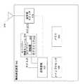
図5は、いくつかの実施の形態に係る例示的な無線通信装置500を示すブロック図である。無線通信装置500は、一以上のRF増幅器508を含む、RFパワー増幅(PA)モジュール504を有してもよい。RFパワー増幅モジュール504は、さらに、一以上のRF増幅器508に接続される、一以上のRFスイッチ512を含んでもよい。RFスイッチ512は、スイッチ回路100および/または400と同様であってもよいし、および/または、スイッチ回路100および/または400を含んでもよい。 FIG. 5 is a block diagram illustrating an example wireless communication apparatus 500 according to some embodiments. The wireless communication device 500 may include an RF power amplification (PA) module 504 that includes one or
RFパワー増幅モジュール504に加えて、無線通信装置500は、少なくとも図示されるように互いに接続される、アンテナ構造514、送受信スイッチ518、送受信機522、メインプロセッサ526およびメモリ530を有してもよい。無線通信装置500は、送信および受信の機能を有するように図示される一方で、他の実施の形態において、送信機能のみ又は受信機能のみを有する装置を含んでもよい。RFスイッチ512は、RFパワー増幅モジュール504に含まれるように図示される一方で、他の実施の形態においては、RFスイッチ512は、RFパワー増幅モジュール504に加えて又は代えて、送受信スイッチ518および/または送受信機522のような、無線通信装置500の他の構成要素に含まれていてもよい。他の実施の形態において、RFスイッチ512は、RFフロントエンド、RF送信器またはパワーコンバータの構成要素であってもよい。 In addition to the RF power amplification module 504, the wireless communication device 500 may include an
種々の実施の形態において、無線通信装置500は、携帯電話、ページング装置、パーソナルデジタルアシスタント、テキストメッセンジャー装置、ポータブルコンピュータ、デスクトップコンピュータ、基地局、加入者局、アクセスポイント、レーダー、衛星通信装置、その他無線によりRF信号を送受信可能ないかなる装置であってもよいが、これらに限定されるものではない。 In various embodiments, the wireless communication device 500 is a mobile phone, paging device, personal digital assistant, text messenger device, portable computer, desktop computer, base station, subscriber station, access point, radar, satellite communication device, etc. Any device that can transmit and receive an RF signal wirelessly may be used, but is not limited thereto.
メインプロセッサ526は、無線通信装置500の全体的な動作を制御するために、メモリ530に記憶される基本的なOS(operating system)プログラムを実行してもよい。例えば、メインプロセッサ526は、送受信機522による信号の受信および送信を制御してもよい。メインプロセッサ526は、メモリ530に常駐する他のプロセスやプログラムを実行する能力を有してもよく、実行するプロセスの要求に応じて、データをメモリ530に移動したり、メモリ530から取り出したりしてもよい。 The
送受信機522は、送信用データ(例えば、音声データ、ウェブデータ、Eメール、通信用データなど)をメインプロセッサ526から取得し、出力用データを意味するRF信号を生成し、RF入力信号をRFパワー増幅モジュール504に供給してもよい。送受信機522はまた、選択された帯域においてRFパワー増幅モジュール504がフルパワーモードもしくはバックオフパワーモードのいずれか一方で動作するように、RFパワー増幅モジュール504を制御してもよい。いくつかの実施の形態において、送受信機522は、OFDM変調を用いるRF入力信号を生成してもよい。 The
RFパワー増幅モジュール504は、ここに記載するように、RF入力信号を増幅してRF出力信号を供給してもよい。RF出力信号は、送受信スイッチ518に転送され、その後、無線(OTA;over-the-air)伝送のためにアンテナ構造514に転送されてもよい。いくつかの実施の形態において、送受信スイッチ518は、デュプレクサを含んでもよい。同様に、送受信機522は、アンテナ構造514から入力される無線(OTA)信号を、送受信スイッチ518を通じて受信してもよい。送受信機522は、入力信号を処理し、さらなる処理のためにメインプロセッサ526へ送信してもよい。 The RF power amplification module 504 may amplify the RF input signal and provide the RF output signal as described herein. The RF output signal may be transferred to transmit / receive
一以上のRFスイッチ512は、無線通信装置500の構成要素の間、および/または、これらの構成要素に対して、RF信号(例えば、RF入力信号および/またはRF出力信号)を選択的に通過するために用いてもよい。 One or more RF switches 512 selectively pass RF signals (eg, RF input signals and / or RF output signals) between and / or relative to the components of wireless communication device 500. It may be used to
種々の実施の形態のいて、アンテナ構造514は、例えば、ダイポールアンテナ、モノポールアンテナ、パッチアンテナ、ループアンテナ、マイクロストリップアンテナまたはRF信号の無線(OTA)送信/受信に適した、いかなる種類のアンテナを含む、一以上の指向性および/または無指向性アンテナを含んでもよい。 In various embodiments, the
当業者であれば、無線通信装置500が例示として示されており、簡潔性および明確性のため、無線通信装置500の大半の構成および動作が、実施の形態の理解のために必要とされる程度に示され、記載されていることが認識されるであろう。種々の実施の形態は、無線通信装置500に関連し、具体的なニーズに従う適切な目的を実行する、いかなる適切な要素または要素の結合を考慮する。さらに言えば、無線通信装置500は、具体的に実施されうる種類の装置に限定されるように解釈すべきではないことが理解されよう。 For those skilled in the art, wireless communication device 500 is shown as an example, and for the sake of brevity and clarity, most configurations and operations of wireless communication device 500 are required for an understanding of the embodiments. It will be appreciated that shown and described to the extent. Various embodiments contemplate any suitable element or combination of elements associated with the wireless communication device 500 and performing an appropriate purpose in accordance with the specific needs. Furthermore, it will be appreciated that the wireless communication device 500 should not be construed as limited to the types of devices that can be specifically implemented.
ここに、方法および装置が提供される。ある実施の形態において、回路は、ソース端子、ゲート端子、ドレイン端子およびボディ端子を含むMOSFETを備えてもよい。回路は、第1抵抗および第2抵抗を有し、ゲート端子とボディ端子の間に接続される抵抗分圧器をさらに備えてもよい。一実施の形態において、MOSFETは、n型MOSFETであってもよい。一実施の形態において、MOSFETは、p型MOSFETであってもよい。いくつかの実施の形態において、第1抵抗は、グランドと接続される第1接続部と、ボディ端子と接続される第2接続部とを備えてもよい。いくつかの実施の形態において、第2抵抗は、ボディ端子と接続される第1接続部と、ゲート端子と接続される第2接続部とを備えてもよい。いくつかの実施の形態において、抵抗分圧器は、ゲート端子の電圧がグランド電圧と等しくないとき、ボディ端子の電圧を、ゲート端子の電圧およびグランド電圧の間にバイアスするように構成されてもよい。他の実施の形態において、ボディ端子の電圧は、第1抵抗の抵抗値および第2抵抗の抵抗値に少なくとも部分的に基づく、既定の電圧であってもよい。一実施の形態において、ゲート端子の電圧は、グランド電圧に対して正であってもよい。一実施の形態において、ゲート端子の電圧は、グランド電圧に対して負であってもよい。一実施の形態において、回路は、MOSFETおよび抵抗分圧器を含むスイッチおよび、このスイッチを含むRFフロントエンド、RF送受信機、またはパワーコンバータをさらに備えてもよい。 Here, methods and apparatus are provided. In some embodiments, the circuit may comprise a MOSFET that includes a source terminal, a gate terminal, a drain terminal, and a body terminal. The circuit may further include a resistance voltage divider having a first resistance and a second resistance and connected between the gate terminal and the body terminal. In one embodiment, the MOSFET may be an n-type MOSFET. In one embodiment, the MOSFET may be a p-type MOSFET. In some embodiments, the first resistor may include a first connection connected to the ground and a second connection connected to the body terminal. In some embodiments, the second resistor may include a first connection connected to the body terminal and a second connection connected to the gate terminal. In some embodiments, the resistive voltage divider may be configured to bias the body terminal voltage between the gate terminal voltage and the ground voltage when the gate terminal voltage is not equal to the ground voltage. . In another embodiment, the body terminal voltage may be a predetermined voltage based at least in part on the resistance value of the first resistor and the resistance value of the second resistor. In one embodiment, the voltage at the gate terminal may be positive with respect to the ground voltage. In one embodiment, the voltage at the gate terminal may be negative with respect to the ground voltage. In one embodiment, the circuit may further comprise a switch including a MOSFET and a resistive voltage divider and an RF front end, RF transceiver, or power converter including the switch.
一実施の形態において、回路は、電源電圧を供給するように構成される電源と、グランド電圧を供給するように構成されるグランド源と、電源およびグランド源に接続される一以上の単位セルとを備えてもよい。一以上の単位セルを構成する単位セルは、ボディ端子、ゲート端子、ソース端子およびドレイン端子を有するMOSFETと、第1抵抗および第2抵抗を備える抵抗分圧器を含み、抵抗分圧器は、ゲート端子の電圧がグランド端子と等しくないとき、ボディ端子の電圧を、ゲート端子の電圧およびグランド電圧の間にバイアスするように構成されてもよい。いくつかの実施の形態において、MOSFETは、p型MOSFETであってもよい。いつかの実施の形態において、MOSFETは、n型MOSFETであってもよい。いくつかの実施の形態において、第1抵抗は、グランド源と接続される第1接続部と、ボディ端子と接続される第2接続部とを備えてもよい。いくつかの実施の形態において、第2抵抗は、ボディ端子と接続される第1接続部と、ゲート端子と接続される第2接続部とを備えてもよい。いくつかの実施の形態において、抵抗分圧器は、ゲート端子とボディ端子の間に接続されてもよい。いくつかの実施の形態において、ボディ端子の電圧は、抵抗分圧器の抵抗値に少なくとも部分的に基づく、既定の電圧であってもよい。いくつかの実施の形態において、ゲート端子の電圧は、グランド電圧に対して正であってもよい。いくつかの実施の形態において、ゲート端子の電圧は、グランド電圧に対して負であってもよい。 In one embodiment, the circuit includes a power supply configured to supply a power supply voltage, a ground source configured to supply a ground voltage, and one or more unit cells connected to the power supply and the ground source. May be provided. A unit cell constituting one or more unit cells includes a MOSFET having a body terminal, a gate terminal, a source terminal, and a drain terminal, and a resistor voltage divider including a first resistor and a second resistor. May be configured to bias the voltage at the body terminal between the voltage at the gate terminal and the ground voltage. In some embodiments, the MOSFET may be a p-type MOSFET. In some embodiments, the MOSFET may be an n-type MOSFET. In some embodiments, the first resistor may include a first connection connected to the ground source and a second connection connected to the body terminal. In some embodiments, the second resistor may include a first connection connected to the body terminal and a second connection connected to the gate terminal. In some embodiments, the resistive voltage divider may be connected between the gate terminal and the body terminal. In some embodiments, the body terminal voltage may be a predetermined voltage based at least in part on the resistance value of the resistive voltage divider. In some embodiments, the voltage at the gate terminal may be positive with respect to the ground voltage. In some embodiments, the voltage at the gate terminal may be negative with respect to the ground voltage.
いくつかの実施の形態は、電源およびグランド源にMOSFETを接続する方法を提供してもよい。MOSFETは、ドレイン端子、ボディ端子、ソース端子およびゲート端子を備えてもよい。この方法は、さらに、抵抗分圧器がボディ端子とゲート端子の間に位置するように、MOSFETのボディ端子およびゲート端子を抵抗分圧器に接続してもよい。第1抵抗の抵抗値および第2抵抗の抵抗値は、ゲート端子がグランド源におけるグランド電圧と等しくないゲート電圧であるときに、ボディ端子に必要とされる電圧に少なくとも部分的に基づいてもよい。いくつかの実施の形態において、MOSFETは、n型MOSFETまたはp型MOSFETであってもよい。いくつかの実施の形態において、この方法は、さらに、第1抵抗の第1接続部をグランド源に接続し、第1抵抗の第2接続部をボディ端子に接続してもよい。いくつかの実施の形態において、この方法は、さらに、第2抵抗の第1端子をゲート端子に接続し、第2抵抗の第2端子をボディ端子に接続してもよい。いくつかの実施の形態において、ボディ端子に必要とされる電圧は、ゲート電圧とグランド電圧の間であってもよい。いくつかの実施の形態において、ゲート電圧は、グランド電圧に対して正であってもよい。いくつかの実施の形態において、ゲート電圧は、グランド電圧に対して負であってもよい。 Some embodiments may provide a method of connecting a MOSFET to a power source and a ground source. The MOSFET may include a drain terminal, a body terminal, a source terminal, and a gate terminal. In this method, the body terminal and the gate terminal of the MOSFET may be further connected to the resistance voltage divider so that the resistance voltage divider is located between the body terminal and the gate terminal. The resistance value of the first resistor and the resistance value of the second resistor may be based at least in part on the voltage required at the body terminal when the gate terminal is a gate voltage that is not equal to the ground voltage at the ground source. . In some embodiments, the MOSFET may be an n-type MOSFET or a p-type MOSFET. In some embodiments, the method may further connect a first connection of the first resistor to a ground source and connect a second connection of the first resistor to the body terminal. In some embodiments, the method may further connect the first terminal of the second resistor to the gate terminal and connect the second terminal of the second resistor to the body terminal. In some embodiments, the voltage required at the body terminal may be between the gate voltage and the ground voltage. In some embodiments, the gate voltage may be positive with respect to the ground voltage. In some embodiments, the gate voltage may be negative with respect to the ground voltage.
本開示は、上述の実施の形態の観点から示されたが、本開示の範囲を逸脱しない限りにおいて、同様の目的を実現すると考えられるさまざまな代替的および/または等価な実施の形態により、上述した特定の実施の形態が置換されてもよいことは、当業者によって理解されるであろう。当業者であれば、本開示によって示された内容が、様々な実施の形態として実施されてもよいことは、すぐに理解されるであろう。本記載は、制限的であるとみなされる代わりに、例示的であるとみなされることを意図する。 Although the present disclosure has been presented in terms of the above-described embodiments, it will be appreciated by those skilled in the art that various alternative and / or equivalent embodiments are contemplated that may achieve similar objectives without departing from the scope of the disclosure. It will be appreciated by those skilled in the art that certain embodiments described above may be substituted. Those skilled in the art will readily appreciate that the subject matter presented by the present disclosure may be implemented as various embodiments. This description is intended to be regarded as illustrative instead of restrictive.
Claims (27)
Translated fromJapanese第1抵抗および第2抵抗を有し、前記ゲート端子および前記ボディ端子の間に接続される抵抗分圧器と、を備える回路。A metal oxide semiconductor field effect transistor (MOSFET) including a source terminal, a gate terminal, a drain terminal and a body terminal;
A circuit having a first resistor and a second resistor, the resistor voltage divider being connected between the gate terminal and the body terminal;
前記スイッチを含む、無線周波数(RF)フロントエンド、RF送信器またはパワーコンバータと、をさらに備える請求項1に記載の回路。A switch including the MOSFET and the resistive voltage divider;
The circuit of claim 1, further comprising a radio frequency (RF) front end, an RF transmitter, or a power converter including the switch.
グランド電圧を供給するように構成されるグランド源と、
前記電源および前記グランド源に接続される一以上の単位セルと、を備え、
前記一以上の単位セルを構成する単位セルは、
ボディ端子、ゲート端子、ソース端子およびドレイン端子を有する金属酸化膜半導体電界効果トランジスタ(MOSFET)と、
第1抵抗および第2抵抗を備える抵抗分圧器と、を有し、
前記抵抗分圧器は、前記ゲート端子の電圧が前記グランド電圧に等しくないときに、前記ボディ端子の電圧を、前記ゲート端子の電圧と前記グランド電圧の間にバイアスするように構成される回路。A power supply configured to supply a power supply voltage;
A ground source configured to provide a ground voltage;
One or more unit cells connected to the power source and the ground source,
Unit cells constituting the one or more unit cells are:
A metal oxide semiconductor field effect transistor (MOSFET) having a body terminal, a gate terminal, a source terminal and a drain terminal;
A resistive voltage divider comprising a first resistor and a second resistor,
The resistor divider is a circuit configured to bias the voltage of the body terminal between the voltage of the gate terminal and the ground voltage when the voltage of the gate terminal is not equal to the ground voltage.
前記MOSFETの前記ボディ端子および前記ゲート端子を、前記ボディ端子および前記ゲート端子の間に抵抗分圧器が位置するように、前記抵抗分圧器に接続し、
第1抵抗の抵抗値および第2抵抗の抵抗値は、前記ゲート端子が前記グランド源におけるグランド電圧と等しくないゲート電圧であるときに、前記ボディ端子に必要とされる電圧に少なくとも部分的に基づく方法。A metal oxide semiconductor field effect transistor (MOSFET) comprising a drain terminal, a body terminal, a source terminal and a gate terminal, connected to a power source and a ground source;
Connecting the body terminal and the gate terminal of the MOSFET to the resistance voltage divider such that a resistance voltage divider is located between the body terminal and the gate terminal;
The resistance value of the first resistor and the resistance value of the second resistor are based at least in part on the voltage required at the body terminal when the gate terminal is a gate voltage not equal to the ground voltage at the ground source. Method.
Applications Claiming Priority (2)
| Application Number | Priority Date | Filing Date | Title |
|---|---|---|---|
| US13/742,086 | 2013-01-15 | ||
| US13/742,086US8847672B2 (en) | 2013-01-15 | 2013-01-15 | Switching device with resistive divider |
Publications (3)
| Publication Number | Publication Date |
|---|---|
| JP2014138423Atrue JP2014138423A (en) | 2014-07-28 |
| JP2014138423A5 JP2014138423A5 (en) | 2017-02-16 |
| JP6574549B2 JP6574549B2 (en) | 2019-09-11 |
Family
ID=51031600
Family Applications (1)
| Application Number | Title | Priority Date | Filing Date |
|---|---|---|---|
| JP2014003422AActiveJP6574549B2 (en) | 2013-01-15 | 2014-01-10 | Switch device with resistive voltage divider |
Country Status (7)
| Country | Link |
|---|---|
| US (1) | US8847672B2 (en) |
| JP (1) | JP6574549B2 (en) |
| KR (1) | KR102110615B1 (en) |
| CN (1) | CN103929163B (en) |
| FR (1) | FR3001097A1 (en) |
| IL (1) | IL230314A (en) |
| TW (1) | TWI608700B (en) |
Cited By (1)
| Publication number | Priority date | Publication date | Assignee | Title |
|---|---|---|---|---|
| US10756724B2 (en) | 2015-03-06 | 2020-08-25 | Qualcomm Incorporated | RF circuit with switch transistor with body connection |
Families Citing this family (15)
| Publication number | Priority date | Publication date | Assignee | Title |
|---|---|---|---|---|
| US20110298432A1 (en) | 2010-06-07 | 2011-12-08 | Skyworks Solutions, Inc | Apparatus and method for variable voltage function |
| EP2568606B1 (en)* | 2011-09-06 | 2014-03-19 | ST-Ericsson SA | Electronic device with body-biasing circuit for portable equipment with USB connector for headset |
| US9373955B2 (en) | 2012-01-09 | 2016-06-21 | Skyworks Solutions, Inc. | Devices and methods related to electrostatic discharge-protected CMOS switches |
| US9214932B2 (en) | 2013-02-11 | 2015-12-15 | Triquint Semiconductor, Inc. | Body-biased switching device |
| US9203396B1 (en)* | 2013-02-22 | 2015-12-01 | Triquint Semiconductor, Inc. | Radio frequency switch device with source-follower |
| US9379698B2 (en) | 2014-02-04 | 2016-06-28 | Triquint Semiconductor, Inc. | Field effect transistor switching circuit |
| TWI580185B (en) | 2015-03-05 | 2017-04-21 | 瑞昱半導體股份有限公司 | Analog switch circuit |
| CN106033961B (en)* | 2015-03-12 | 2019-09-03 | 瑞昱半导体股份有限公司 | Analog switch circuit |
| KR101901699B1 (en) | 2016-10-05 | 2018-09-28 | 삼성전기 주식회사 | Antenna switch circuit with improved harmonic suppression characteristic |
| US11320158B2 (en)* | 2017-05-11 | 2022-05-03 | Coway Co., Ltd. | Multifunctional circulation system enabling purification of outside air |
| CN109150150A (en)* | 2018-08-06 | 2019-01-04 | 上海华虹宏力半导体制造有限公司 | A kind of radio-frequency switch circuit improving RF switch characteristic |
| US10854596B2 (en)* | 2018-11-29 | 2020-12-01 | Berex, Inc. | CMOS RF power limiter and ESD protection circuits |
| JP7337561B2 (en)* | 2019-06-25 | 2023-09-04 | ローム株式会社 | analog switch circuit, volume circuit, semiconductor integrated circuit |
| US11585844B1 (en)* | 2021-09-09 | 2023-02-21 | Board Of Regents, The University Of Texas System | Systems, circuits, and methods to detect gate-open failures in MOS based insulated gate transistors |
| TWI870135B (en)* | 2023-12-01 | 2025-01-11 | 立積電子股份有限公司 | Semiconductor device |
Citations (8)
| Publication number | Priority date | Publication date | Assignee | Title |
|---|---|---|---|---|
| US5959488A (en)* | 1998-01-24 | 1999-09-28 | Winbond Electronics Corp. | Dual-node capacitor coupled MOSFET for improving ESD performance |
| JP2004007212A (en)* | 2002-05-31 | 2004-01-08 | Fujitsu Ltd | I / O buffer, input buffer and output buffer |
| JP2004296795A (en)* | 2003-03-27 | 2004-10-21 | National Institute Of Advanced Industrial & Technology | Double gate field effect transistor |
| WO2006011364A1 (en)* | 2004-07-28 | 2006-02-02 | Matsushita Electric Industrial Co., Ltd. | Oscillator |
| JP2006041232A (en)* | 2004-07-28 | 2006-02-09 | Matsushita Electric Ind Co Ltd | High frequency circuit |
| JP2009065304A (en)* | 2007-09-05 | 2009-03-26 | Panasonic Corp | High frequency switch device |
| JP2010028352A (en)* | 2008-07-17 | 2010-02-04 | Ricoh Co Ltd | Inverter circuit |
| US20100156511A1 (en)* | 2008-12-23 | 2010-06-24 | International Business Machines Corporation | Bias voltage generation circuit for an soi radio frequency switch |
Family Cites Families (80)
| Publication number | Priority date | Publication date | Assignee | Title |
|---|---|---|---|---|
| US3551788A (en) | 1968-09-13 | 1970-12-29 | Servo Corp Of America | High voltage transistorized stack with leakage current compensation |
| US3699359A (en) | 1971-04-20 | 1972-10-17 | Philco Ford Corp | Electronic latching device |
| US4053916A (en) | 1975-09-04 | 1977-10-11 | Westinghouse Electric Corporation | Silicon on sapphire MOS transistor |
| DE2851789C2 (en) | 1978-11-30 | 1981-10-01 | Licentia Patent-Verwaltungs-Gmbh, 6000 Frankfurt | Circuit for switching and transmitting alternating voltages |
| US4491750A (en) | 1982-09-28 | 1985-01-01 | Eaton Corporation | Bidirectionally source stacked FETs with drain-referenced common gating |
| JPH01254014A (en) | 1988-04-04 | 1989-10-11 | Toshiba Corp | power amplifier |
| JPH07105447B2 (en) | 1988-12-15 | 1995-11-13 | 株式会社東芝 | Transmission gate |
| US5313083A (en) | 1988-12-16 | 1994-05-17 | Raytheon Company | R.F. switching circuits |
| US5105164A (en) | 1989-02-28 | 1992-04-14 | At&T Bell Laboratories | High efficiency uhf linear power amplifier |
| US5012123A (en) | 1989-03-29 | 1991-04-30 | Hittite Microwave, Inc. | High-power rf switching system |
| JPH0732335B2 (en) | 1990-11-16 | 1995-04-10 | 日本電信電話株式会社 | High frequency amplifier |
| JP3243892B2 (en) | 1993-05-21 | 2002-01-07 | ソニー株式会社 | Signal switch |
| US5930638A (en) | 1993-07-12 | 1999-07-27 | Peregrine Semiconductor Corp. | Method of making a low parasitic resistor on ultrathin silicon on insulator |
| US5973382A (en) | 1993-07-12 | 1999-10-26 | Peregrine Semiconductor Corporation | Capacitor on ultrathin semiconductor on insulator |
| US5973363A (en) | 1993-07-12 | 1999-10-26 | Peregrine Semiconductor Corp. | CMOS circuitry with shortened P-channel length on ultrathin silicon on insulator |
| US5863823A (en) | 1993-07-12 | 1999-01-26 | Peregrine Semiconductor Corporation | Self-aligned edge control in silicon on insulator |
| US5416043A (en) | 1993-07-12 | 1995-05-16 | Peregrine Semiconductor Corporation | Minimum charge FET fabricated on an ultrathin silicon on sapphire wafer |
| US5572040A (en) | 1993-07-12 | 1996-11-05 | Peregrine Semiconductor Corporation | High-frequency wireless communication system on a single ultrathin silicon on sapphire chip |
| US5452473A (en) | 1994-02-28 | 1995-09-19 | Qualcomm Incorporated | Reverse link, transmit power correction and limitation in a radiotelephone system |
| US5553295A (en) | 1994-03-23 | 1996-09-03 | Intel Corporation | Method and apparatus for regulating the output voltage of negative charge pumps |
| JP2801563B2 (en) | 1994-08-30 | 1998-09-21 | 松下電器産業株式会社 | Transmission / reception circuit of communication radio, semiconductor integrated circuit device, and communication radio |
| JPH08148949A (en) | 1994-11-18 | 1996-06-07 | Fujitsu Ltd | High frequency amplifier |
| FR2742942B1 (en) | 1995-12-26 | 1998-01-16 | Sgs Thomson Microelectronics | HIGH VOLTAGE SLOT GENERATOR |
| US5777530A (en) | 1996-01-31 | 1998-07-07 | Matsushita Electric Industrial Co., Ltd. | Switch attenuator |
| JP3484462B2 (en) | 1996-04-11 | 2004-01-06 | 株式会社ルネサステクノロジ | Method for estimating lifetime of floating SOI-MOSFET |
| JPH09284114A (en) | 1996-04-19 | 1997-10-31 | Toshiba Microelectron Corp | Analog input circuit |
| US5689144A (en)* | 1996-05-15 | 1997-11-18 | Siliconix Incorporated | Four-terminal power MOSFET switch having reduced threshold voltage and on-resistance |
| GB2331879B (en) | 1996-08-05 | 2001-03-28 | Mitsubishi Electric Corp | Radio-frequency integrated circuit for a radio-frequency wireless transmitter-receiver with reduced influence by radio-frequency power leakage |
| US5818099A (en) | 1996-10-03 | 1998-10-06 | International Business Machines Corporation | MOS high frequency switch circuit using a variable well bias |
| US5920233A (en) | 1996-11-18 | 1999-07-06 | Peregrine Semiconductor Corp. | Phase locked loop including a sampling circuit for reducing spurious side bands |
| JPH10242829A (en) | 1997-02-24 | 1998-09-11 | Sanyo Electric Co Ltd | Switch circuit device |
| JP3441330B2 (en) | 1997-02-28 | 2003-09-02 | 株式会社東芝 | Semiconductor device and manufacturing method thereof |
| US6160292A (en) | 1997-04-23 | 2000-12-12 | International Business Machines Corporation | Circuit and methods to improve the operation of SOI devices |
| US6033974A (en) | 1997-05-12 | 2000-03-07 | Silicon Genesis Corporation | Method for controlled cleaving process |
| US6245161B1 (en) | 1997-05-12 | 2001-06-12 | Silicon Genesis Corporation | Economical silicon-on-silicon hybrid wafer assembly |
| US6180496B1 (en) | 1997-08-29 | 2001-01-30 | Silicon Genesis Corporation | In situ plasma wafer bonding method |
| JPH11136111A (en) | 1997-10-30 | 1999-05-21 | Sony Corp | High frequency circuit |
| JP3711193B2 (en) | 1998-01-16 | 2005-10-26 | 三菱電機株式会社 | Transmission / reception switching circuit |
| US6271067B1 (en)* | 1998-02-27 | 2001-08-07 | Micron Technology, Inc. | Methods of forming field effect transistors and field effect transistor circuitry |
| US6249027B1 (en) | 1998-06-08 | 2001-06-19 | Sun Microsystems, Inc. | Partially depleted SOI device having a dedicated single body bias means |
| JP2000022160A (en) | 1998-07-06 | 2000-01-21 | Hitachi Ltd | Semiconductor integrated circuit and method of manufacturing the same |
| JP4360702B2 (en) | 1998-08-07 | 2009-11-11 | 株式会社ルネサステクノロジ | Semiconductor device |
| JP3408762B2 (en) | 1998-12-03 | 2003-05-19 | シャープ株式会社 | Semiconductor device having SOI structure and method of manufacturing the same |
| US6171965B1 (en) | 1999-04-21 | 2001-01-09 | Silicon Genesis Corporation | Treatment method of cleaved film for the manufacture of substrates |
| AU6905000A (en) | 1999-08-10 | 2001-03-05 | Silicon Genesis Corporation | A cleaving process to fabricate multilayered substrates using low implantation doses |
| US6628159B2 (en)* | 1999-09-17 | 2003-09-30 | International Business Machines Corporation | SOI voltage-tolerant body-coupled pass transistor |
| JP3608456B2 (en) | 1999-12-08 | 2005-01-12 | セイコーエプソン株式会社 | Manufacturing method of SOI structure MIS field effect transistor |
| US6504212B1 (en) | 2000-02-03 | 2003-01-07 | International Business Machines Corporation | Method and apparatus for enhanced SOI passgate operations |
| JP3504212B2 (en) | 2000-04-04 | 2004-03-08 | シャープ株式会社 | Semiconductor device with SOI structure |
| JP2002033399A (en) | 2000-07-13 | 2002-01-31 | Toshiba Corp | Semiconductor integrated circuit and its manufacturing method |
| US6816016B2 (en) | 2000-08-10 | 2004-11-09 | Tropian, Inc. | High-efficiency modulating RF amplifier |
| US6496074B1 (en) | 2000-09-28 | 2002-12-17 | Koninklijke Philips Electronics N.V. | Cascode bootstrapped analog power amplifier circuit |
| US6978437B1 (en) | 2000-10-10 | 2005-12-20 | Toppan Photomasks, Inc. | Photomask for eliminating antenna effects in an integrated circuit and integrated circuit manufacture with same |
| JP4434474B2 (en) | 2000-11-29 | 2010-03-17 | Necエレクトロニクス株式会社 | MOS transistor simulation test method |
| TWI230392B (en) | 2001-06-18 | 2005-04-01 | Innovative Silicon Sa | Semiconductor device |
| US6819938B2 (en) | 2001-06-26 | 2004-11-16 | Qualcomm Incorporated | System and method for power control calibration and a wireless communication device |
| KR100906356B1 (en) | 2001-08-10 | 2009-07-06 | 히타치 긴조쿠 가부시키가이샤 | Bypass filter |
| JP3986780B2 (en) | 2001-08-17 | 2007-10-03 | 三菱電機株式会社 | Complementary push-pull amplifier |
| US7796969B2 (en) | 2001-10-10 | 2010-09-14 | Peregrine Semiconductor Corporation | Symmetrically and asymmetrically stacked transistor group RF switch |
| US6804502B2 (en) | 2001-10-10 | 2004-10-12 | Peregrine Semiconductor Corporation | Switch circuit and method of switching radio frequency signals |
| JP3813869B2 (en) | 2001-12-20 | 2006-08-23 | 松下電器産業株式会社 | Field effect transistor switch circuit |
| US6642578B1 (en) | 2002-07-22 | 2003-11-04 | Anadigics, Inc. | Linearity radio frequency switch with low control voltage |
| KR100496863B1 (en)* | 2002-10-04 | 2005-06-22 | 삼성전자주식회사 | Power-on reset circuit |
| JP3445608B2 (en) | 2002-10-25 | 2003-09-08 | 株式会社東芝 | Digital information management system including video information |
| JP2004205301A (en) | 2002-12-25 | 2004-07-22 | Nec Corp | Evaluation device and circuit designing method used therefor |
| JP4342970B2 (en) | 2004-02-02 | 2009-10-14 | 株式会社東芝 | Semiconductor memory device and manufacturing method thereof |
| US7042044B2 (en) | 2004-02-18 | 2006-05-09 | Koucheng Wu | Nor-type channel-program channel-erase contactless flash memory on SOI |
| US7072217B2 (en) | 2004-02-24 | 2006-07-04 | Micron Technology, Inc. | Multi-state memory cell with asymmetric charge trapping |
| US7158067B2 (en)* | 2005-01-31 | 2007-01-02 | The United States Of America As Represented By The Secretary Of The Navy | Analog to digital converter using sawtooth voltage signals with differential comparator |
| US7402850B2 (en) | 2005-06-21 | 2008-07-22 | Micron Technology, Inc. | Back-side trapped non-volatile memory device |
| US8742502B2 (en) | 2005-07-11 | 2014-06-03 | Peregrine Semiconductor Corporation | Method and apparatus for use in improving linearity of MOSFETs using an accumulated charge sink-harmonic wrinkle reduction |
| US20080076371A1 (en) | 2005-07-11 | 2008-03-27 | Alexander Dribinsky | Circuit and method for controlling charge injection in radio frequency switches |
| US7890891B2 (en) | 2005-07-11 | 2011-02-15 | Peregrine Semiconductor Corporation | Method and apparatus improving gate oxide reliability by controlling accumulated charge |
| US7910993B2 (en) | 2005-07-11 | 2011-03-22 | Peregrine Semiconductor Corporation | Method and apparatus for use in improving linearity of MOSFET's using an accumulated charge sink |
| US20070023833A1 (en) | 2005-07-28 | 2007-02-01 | Serguei Okhonin | Method for reading a memory cell having an electrically floating body transistor, and memory cell and array implementing same |
| WO2007018037A1 (en) | 2005-08-09 | 2007-02-15 | Hitachi Metals, Ltd. | High-frequency switch circuit |
| US7863691B2 (en) | 2008-03-10 | 2011-01-04 | International Business Machines Corporation | Merged field effect transistor cells for switching |
| JP5632663B2 (en)* | 2010-06-29 | 2014-11-26 | ルネサスエレクトロニクス株式会社 | Semiconductor device |
| US9160328B2 (en)* | 2012-07-07 | 2015-10-13 | Skyworks Solutions, Inc. | Circuits, devices, methods and applications related to silicon-on-insulator based radio-frequency switches |
| JP5575348B1 (en) | 2014-01-20 | 2014-08-20 | 株式会社Leap | Connector manufacturing method |
- 2013
- 2013-01-15USUS13/742,086patent/US8847672B2/enactiveActive
- 2014
- 2014-01-02ILIL230314Apatent/IL230314A/enactiveIP Right Grant
- 2014-01-07TWTW103100486Apatent/TWI608700B/enactive
- 2014-01-08FRFR1450111Apatent/FR3001097A1/ennot_activeWithdrawn
- 2014-01-10JPJP2014003422Apatent/JP6574549B2/enactiveActive
- 2014-01-14KRKR1020140004273Apatent/KR102110615B1/enactiveActive
- 2014-01-14CNCN201410016473.0Apatent/CN103929163B/ennot_activeExpired - Fee Related
Patent Citations (8)
| Publication number | Priority date | Publication date | Assignee | Title |
|---|---|---|---|---|
| US5959488A (en)* | 1998-01-24 | 1999-09-28 | Winbond Electronics Corp. | Dual-node capacitor coupled MOSFET for improving ESD performance |
| JP2004007212A (en)* | 2002-05-31 | 2004-01-08 | Fujitsu Ltd | I / O buffer, input buffer and output buffer |
| JP2004296795A (en)* | 2003-03-27 | 2004-10-21 | National Institute Of Advanced Industrial & Technology | Double gate field effect transistor |
| WO2006011364A1 (en)* | 2004-07-28 | 2006-02-02 | Matsushita Electric Industrial Co., Ltd. | Oscillator |
| JP2006041232A (en)* | 2004-07-28 | 2006-02-09 | Matsushita Electric Ind Co Ltd | High frequency circuit |
| JP2009065304A (en)* | 2007-09-05 | 2009-03-26 | Panasonic Corp | High frequency switch device |
| JP2010028352A (en)* | 2008-07-17 | 2010-02-04 | Ricoh Co Ltd | Inverter circuit |
| US20100156511A1 (en)* | 2008-12-23 | 2010-06-24 | International Business Machines Corporation | Bias voltage generation circuit for an soi radio frequency switch |
Cited By (2)
| Publication number | Priority date | Publication date | Assignee | Title |
|---|---|---|---|---|
| US10756724B2 (en) | 2015-03-06 | 2020-08-25 | Qualcomm Incorporated | RF circuit with switch transistor with body connection |
| US11539360B2 (en) | 2015-03-06 | 2022-12-27 | Qualcomm Incorporated | RF switch having independently generated gate and body voltages |
Also Published As
| Publication number | Publication date |
|---|---|
| CN103929163A (en) | 2014-07-16 |
| FR3001097A1 (en) | 2014-07-18 |
| IL230314A (en) | 2016-06-30 |
| JP6574549B2 (en) | 2019-09-11 |
| CN103929163B (en) | 2019-03-22 |
| US8847672B2 (en) | 2014-09-30 |
| TWI608700B (en) | 2017-12-11 |
| TW201429161A (en) | 2014-07-16 |
| IL230314A0 (en) | 2014-08-31 |
| KR102110615B1 (en) | 2020-05-28 |
| KR20140092256A (en) | 2014-07-23 |
| US20140197882A1 (en) | 2014-07-17 |
Similar Documents
| Publication | Publication Date | Title |
|---|---|---|
| JP6574549B2 (en) | Switch device with resistive voltage divider | |
| JP6800926B2 (en) | Body biased switch device | |
| TWI604694B (en) | Switching device with non-negative biasing | |
| JP6600448B2 (en) | Bias enhancement bias circuit for radio frequency power amplifiers. | |
| JP6616949B2 (en) | Low noise amplifier drain switch circuit | |
| US8977217B1 (en) | Switching device with negative bias circuit | |
| JP6616947B2 (en) | Bias circuit for high power high frequency switching element | |
| KR102189055B1 (en) | P-tunneling field effect transistor device with pocket | |
| US8923782B1 (en) | Switching device with diode-biased field-effect transistor (FET) | |
| US9203396B1 (en) | Radio frequency switch device with source-follower | |
| US11088685B2 (en) | High-frequency switch | |
| JP2010278110A (en) | Semiconductor device and high-frequency switch circuit |
Legal Events
| Date | Code | Title | Description |
|---|---|---|---|
| A521 | Request for written amendment filed | Free format text:JAPANESE INTERMEDIATE CODE: A523 Effective date:20140318 | |
| A521 | Request for written amendment filed | Free format text:JAPANESE INTERMEDIATE CODE: A523 Effective date:20170106 | |
| A621 | Written request for application examination | Free format text:JAPANESE INTERMEDIATE CODE: A621 Effective date:20170106 | |
| A977 | Report on retrieval | Free format text:JAPANESE INTERMEDIATE CODE: A971007 Effective date:20171013 | |
| A131 | Notification of reasons for refusal | Free format text:JAPANESE INTERMEDIATE CODE: A131 Effective date:20171114 | |
| A601 | Written request for extension of time | Free format text:JAPANESE INTERMEDIATE CODE: A601 Effective date:20180213 | |
| A521 | Request for written amendment filed | Free format text:JAPANESE INTERMEDIATE CODE: A523 Effective date:20180406 | |
| A131 | Notification of reasons for refusal | Free format text:JAPANESE INTERMEDIATE CODE: A131 Effective date:20180925 | |
| A601 | Written request for extension of time | Free format text:JAPANESE INTERMEDIATE CODE: A601 Effective date:20181225 | |
| A521 | Request for written amendment filed | Free format text:JAPANESE INTERMEDIATE CODE: A523 Effective date:20190221 | |
| TRDD | Decision of grant or rejection written | ||
| A01 | Written decision to grant a patent or to grant a registration (utility model) | Free format text:JAPANESE INTERMEDIATE CODE: A01 Effective date:20190730 | |
| A61 | First payment of annual fees (during grant procedure) | Free format text:JAPANESE INTERMEDIATE CODE: A61 Effective date:20190819 | |
| R150 | Certificate of patent or registration of utility model | Ref document number:6574549 Country of ref document:JP Free format text:JAPANESE INTERMEDIATE CODE: R150 | |
| R250 | Receipt of annual fees | Free format text:JAPANESE INTERMEDIATE CODE: R250 | |
| R250 | Receipt of annual fees | Free format text:JAPANESE INTERMEDIATE CODE: R250 | |
| R250 | Receipt of annual fees | Free format text:JAPANESE INTERMEDIATE CODE: R250 | |
| R250 | Receipt of annual fees | Free format text:JAPANESE INTERMEDIATE CODE: R250 |