JP2014135515A - Solid state image pickup device - Google Patents
Solid state image pickup deviceDownload PDFInfo
- Publication number
- JP2014135515A JP2014135515AJP2014079699AJP2014079699AJP2014135515AJP 2014135515 AJP2014135515 AJP 2014135515AJP 2014079699 AJP2014079699 AJP 2014079699AJP 2014079699 AJP2014079699 AJP 2014079699AJP 2014135515 AJP2014135515 AJP 2014135515A
- Authority
- JP
- Japan
- Prior art keywords
- semiconductor region
- region
- type semiconductor
- mos transistor
- gate electrode
- Prior art date
- Legal status (The legal status is an assumption and is not a legal conclusion. Google has not performed a legal analysis and makes no representation as to the accuracy of the status listed.)
- Pending
Links
- 239000007787solidSubstances0.000titleabstract3
- 239000004065semiconductorSubstances0.000claimsabstractdescription45
- 238000006243chemical reactionMethods0.000claimsabstractdescription26
- 238000003384imaging methodMethods0.000claimsdescription37
- 230000002093peripheral effectEffects0.000claimsdescription2
- 239000012535impuritySubstances0.000description11
- 238000010586diagramMethods0.000description7
- 230000003321amplificationEffects0.000description5
- 238000003199nucleic acid amplification methodMethods0.000description5
- 239000000758substrateSubstances0.000description5
- 229910004298SiO 2Inorganic materials0.000description3
- 238000005036potential barrierMethods0.000description3
- 238000009825accumulationMethods0.000description2
- 238000005468ion implantationMethods0.000description2
- 230000015572biosynthetic processEffects0.000description1
- 239000002131composite materialSubstances0.000description1
- 238000009792diffusion processMethods0.000description1
- 238000005530etchingMethods0.000description1
- 238000011835investigationMethods0.000description1
- 238000002955isolationMethods0.000description1
- 238000004519manufacturing processMethods0.000description1
- 238000000034methodMethods0.000description1
- 238000012986modificationMethods0.000description1
- 230000004048modificationEffects0.000description1
- 230000003647oxidationEffects0.000description1
- 238000007254oxidation reactionMethods0.000description1
- 230000001590oxidative effectEffects0.000description1
- 229910021420polycrystalline siliconInorganic materials0.000description1
- 229910052710siliconInorganic materials0.000description1
- 239000010703siliconSubstances0.000description1
Images


Landscapes
- Solid State Image Pick-Up Elements (AREA)
- Transforming Light Signals Into Electric Signals (AREA)
Abstract
Description
Translated fromJapanese本発明は、固体撮像装置、特にMOSトランジスタ(本明細書でいうMOSとは、導電層/絶縁膜/半導体構造を総称するものとする。)を有するMOS型の固体撮像装置とその製造方法に係わる。 The present invention relates to a solid-state imaging device, in particular a MOS type solid-state imaging device having a MOS transistor (herein, MOS is a generic term for a conductive layer / insulating film / semiconductor structure) and a method for manufacturing the same. Involved.
図1は、いわゆるFD(Floating Diffusion) 型構成によるMOS型固体撮像装置の要部の構成図を示す。この固体撮像装置は、それぞれ複数の行および列、すなわち水平および垂直方向にそれぞれ複数の単位画素101(図1においては、1つの単位画素のみを示す)が配列され、各単位画素101が、光電変換素子のフォトダイオード102によるセンサー部と、このセンサー部で得た信号電荷をFD読み出しMOSトランジスタ103によって読み出し、この信号電荷を、各単位画素においてFD増幅MOSトランジスタ104によって信号電圧もしくは信号電流に増幅する構成とされている。 FIG. 1 shows a configuration diagram of a main part of a MOS type solid-state imaging device having a so-called FD (Floating Diffusion) type configuration. In this solid-state imaging device, a plurality of unit pixels 101 (only one unit pixel is shown in FIG. 1) are arranged in a plurality of rows and columns, that is, in the horizontal and vertical directions, respectively. The sensor unit by the
図1の構成においては、各単位画素101において信号の増幅を行う構成とした場合であるが、図2にその要部の構成図を示すように、例えば共通の列毎に増幅器が配置されたいわゆるカラムアンプ型固体撮像装置とすることができる。 In the configuration of FIG. 1, the signal amplification is performed in each
このカラムアンプ型固体撮像装置においてもそれぞれ複数の行および列、すなわち水平および垂直方向にそれぞれ複数の単位画素201(図2においても、1つの単位画素のみを示す)が配列され、各単位画素201は、そのセンサー部に光電変換素子としてのフォトダイオード202を有し、このフォトダイオード202に蓄積された信号電荷を読み出すMOSトランジスタ203と、信号電荷を垂直信号線208に読み出す選択用MOSトランジスタ204が形成され、垂直信号線208毎にカラム増幅器205が配置された構成を有する。 Also in this column amplifier type solid-state imaging device, a plurality of unit pixels 201 (only one unit pixel is shown in FIG. 2) are arranged in a plurality of rows and columns, that is, in the horizontal and vertical directions. Has a
これらMOS型の固体撮像装置の各単位画素101,201における、センサー部の光電変換素子、すなわちフォトダイオードと、これからの電荷読み出しを行うMOSトランジスタとは、フォトダイオードを構成する一方の半導体領域例えばカソード領域をMOSトランジスタのソース領域と兼ねしめる複合構成とされる。 In each of the
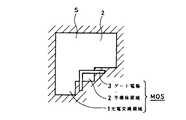
図6は、このセンサー部Sと、これからの信号電荷の読み出しを行うMOSトランジスタの形成部の概略平面パターン図を示す。センサー部Sは、フォトダイオードを構成する光電変換領域1が形成されてなる。MOSトランジスタ(MOS)は、光電変換領域1と所要の距離、すなわちチャンネル長に相当する距離を隔てて形成された半導体領域2とをソースおよびドレインとして、これら間にゲート絶縁膜(図示せず)を介してゲート電極3が形成されることによって構成される。 FIG. 6 shows a schematic plan pattern diagram of the sensor portion S and the formation portion of the MOS transistor for reading signal charges from now on. The sensor unit S is formed with a photoelectric conversion region 1 constituting a photodiode. The MOS transistor (MOS) has a gate insulating film (not shown) between a photoelectric conversion region 1 and a semiconductor region 2 formed at a required distance, that is, a distance corresponding to a channel length, as a source and a drain. The
センサー部Sは、例えば図1および図2で説明した単位画素101および201内における一隅に形成され、ゲート電極3は、単位画素内における他の回路素子形成部側に偏寄って形成される。 The sensor unit S is formed at one corner in the
上述のMOS型撮像装置は、MOSトランジスタによることから、例えばCCD(電荷結合素子)型撮像装置に比し、本来、低消費電力化できるという利点を有するものであるが、上述したセンサー部から信号電荷を、読み出しトランジスタによって、低い読み出し電圧で完全に信号電荷読み出しを行うことに問題が生じている。 Since the above-described MOS type imaging device is based on a MOS transistor, it has an advantage that lower power consumption can be achieved compared to a CCD (charge coupled device) type imaging device. There is a problem in completely reading out signal charges with a read transistor at a low read voltage.
本発明においては、このような問題の解決を図る。すなわち、本発明者は、上述した読み出しMOSトランジスタにおける読み出し電圧と信号電荷の読み出しの不完全の原因が、センサー部と読み出しのMOSトランジスタのゲート部との位置関係に起因していることを究明した。すなわち、従来構造による場合、センサー部の光電変換領域における信号電荷に対するポテンシャルの窪みに対して、ゲート電極の配置位置が離れて形成されていることによって、信号電荷の読み出しを行うに、その読み出しMOSトランジスタに対する読み出し電圧すなわちゲート電圧を大きくすることが必要となり、また信号電荷を完全に読み出すことが困難であり、この読み出しを完全に行うためには、更に大きな読み出し電圧を必要とすることになることを究明した。本発明においては、この究明に基いて、センサー部から信号電荷を、低い読み出し電圧でほぼ完全に読み出すことができるようにした固体撮像装置、特にMOS撮像装置を提供するものである。 In the present invention, such a problem is solved. That is, the present inventor has determined that the cause of the incomplete reading of the reading voltage and the signal charge in the reading MOS transistor described above is due to the positional relationship between the sensor portion and the gate portion of the reading MOS transistor. . That is, in the case of the conventional structure, the readout MOS is used to read out the signal charge because the gate electrode is arranged away from the potential depression for the signal charge in the photoelectric conversion region of the sensor unit. It is necessary to increase the read voltage for the transistor, that is, the gate voltage, and it is difficult to read out the signal charges completely. To read out completely, a larger read voltage is required. Investigated. In the present invention, based on this investigation, a solid-state imaging device, particularly a MOS imaging device, which can read out signal charges from a sensor section almost completely with a low readout voltage is provided.
本発明による固体撮像装置は、複数の単位画素で構成され、単位画素は、第1のN型半導体領域と該N型半導体領域の上部に形成されたP型半導体領域で構成され、光照射により発生した信号電荷を該N型半導体領域に蓄積する光電変換領域と、この光電変換領域から信号電荷を読み出すMOSトランジスタのゲート電極と、MOSトランジスタのドレイン領域でかつ光電変換領域から信号電荷を読み出す先である第2のN型半導体領域と、第1のN型半導体領域の外側に配置されたチャネルストップ領域とを有し、ゲート電極は、そのチャネル幅方向に関するゲート電極の中間部において、第1のN型半導体領域に向かって凸の屈曲ないしは湾曲パターンで形成される。 The solid-state imaging device according to the present invention includes a plurality of unit pixels, and each unit pixel includes a first N-type semiconductor region and a P-type semiconductor region formed on the N-type semiconductor region. A photoelectric conversion region that accumulates the generated signal charge in the N-type semiconductor region, a gate electrode of a MOS transistor that reads the signal charge from the photoelectric conversion region, and a destination that reads the signal charge from the photoelectric conversion region in the drain region of the MOS transistor A second N-type semiconductor region and a channel stop region arranged outside the first N-type semiconductor region, and the gate electrode is formed in the middle portion of the gate electrode in the channel width direction. It is formed in a convex bent or curved pattern toward the N-type semiconductor region.
上述したように、本発明においては、ゲート電極を、そのチャネル幅方向に関するゲート電極の中間部において、第1のN型半導体領域に向かって凸の屈曲ないしは湾曲パターンで形成したことから、チャネルストップ領域によるポテンシャルバリアの最も高い部分より低い部分から信号電荷の読み出しがなされることから、読み出し電圧を低めることができ、しかもこの信号電荷の読み出しをほぼ完全に行うことができる。 As described above, in the present invention, since the gate electrode is formed in a convex or curved pattern toward the first N-type semiconductor region in the intermediate portion of the gate electrode in the channel width direction, the channel stop Since the signal charge is read from a portion lower than the highest potential barrier in the region, the read voltage can be lowered and the signal charge can be read almost completely.
上述したように、本発明による固体撮像装置によれば、信号電荷の読み出し電圧の低減化と、信号電荷のほぼ完全な読み出しを可能にする。したがって、MOS型固体撮像装置における駆動電圧、したがって、消費電力の低減化の特長をより助長することができる。 As described above, according to the solid-state imaging device according to the present invention, it is possible to reduce the signal charge read voltage and to read the signal charge almost completely. Therefore, the driving voltage in the MOS type solid-state imaging device, and hence the feature of reducing the power consumption can be further promoted.
本発明によるMOS型固体撮像装置の一形態は、図1のFD型のMOS型固体撮像装置とすることができる。この固体撮像装置は、前述したように、それぞれ複数の行および列、すなわち水平および垂直方向にそれぞれ複数の単位画素101が配列され、各単位画素101が、光電変換がなされるセンサー部と、このセンサー部で得た信号電荷をMOSトランジスタ103によって読み出し、この信号電荷を、各単位画素においてMOSトランジスタ104のよって信号電圧もしくは信号電流に増幅する構成としたいわゆるの増幅型撮像装置とする。 One embodiment of the MOS solid-state imaging device according to the present invention can be the FD-type MOS solid-state imaging device of FIG. As described above, this solid-state imaging device includes a plurality of
この固体撮像装置の単位画素101は、そのセンサー部に光電変換素子としてのフォトダイオード102を有し、このフォトダイオード102に蓄積された信号電荷を読み出すFD読み出しMOSトランジスタ103と、FD増幅MOSトランジスタ104と、FDリセットMOSトランジスタ105と、垂直選択MOSトランジスタ106とを有してなる。 The
FD読み出しMOSトランジスタ103のゲート電極は、垂直読み出し線107に接続され、FDリセットMOSトランジスタ105のゲート電極は、垂直リセット線108に接続され、垂直選択MOSトランジスタ106のゲート電極は、垂直選択線に接続され、垂直選択MOSトランジスタ106のソースが垂直信号線110にそれぞれ接続される。 The gate electrode of the FD read
111は、水平信号線で、この水平信号線111と垂直信号線110との間に水平選択MOSトランジスタ112が接続され、このMOSトランジスタ112のゲート電極に、水平走査回路113からの水平走査パルスφHmが、印加される。そして、行選択をする垂直走査回路114からの垂直走査パルスφvSn,φvtn,φvRnにより各行ごとに各単位画素101において、フォトダイオード102に蓄積された信号電荷が、読み出しMOSトランジスタ103によって読み出され、増幅MOSトランジスタ104によって増幅され、垂直選択MOSトランジスタ106によって選択される。そして、列選択する水平走査回路113からの水平走査パルスφHmにより制御される水平選択MOSトランジスタ112を通じて各画素信号が水平線111に出力される。一方、リセットMOSトランジスタ105によって各単位画素101のリセットがなされる。Reference numeral 111 denotes a horizontal signal line. A horizontal
また、本発明によるMOSトランジスタ型固体撮像装置の他の一形態は、図2で示したいわゆるコラムアンプ型によるMOS型固体撮像装置を構成することができる。この固体撮像装置についても、すでに説明したように、共通の列毎に増幅器が配置される。この固体撮像装置においてもそれぞれ複数の行および列、すなわち水平および垂直方向にそれぞれ複数の単位画素201が配列され、各単位画素201が、そのセンサー部に光電変換素子としてのフォトダイオード202を有し、このフォトダイオード202に蓄積された信号電荷を読み出す選択用MOSトランジスタ203を有し、この信号電荷を垂直信号線208に読み出す水平読み出しMOSトランジスタ204を有して成る。 Another embodiment of the MOS transistor type solid-state imaging device according to the present invention can constitute the so-called column amplifier type MOS solid-state imaging device shown in FIG. Also in this solid-state imaging device, as already described, an amplifier is arranged for each common column. Also in this solid-state imaging device, a plurality of unit pixels 201 are arranged respectively in a plurality of rows and columns, that is, in the horizontal and vertical directions, and each unit pixel 201 has a
MOSトランジスタ203は、そのゲート電極への垂直走査回路214からの垂直走査パルスの印加によってオンされる電荷読み出しのいわばスイッチ機能を有し、MOSトランジスタ204は、そのゲート電極に水平走査回路213からの水平走査パルスが印加されることによって信号電荷を垂直信号線208に読み出す。そして、この垂直信号線208に読み出された信号電荷を増幅器205によって増幅し、水平選択MOSトランジスタ206によって、選択された列上の単位画素からの信号電荷による出力を水平信号線207に出力するようになされる。 The MOS transistor 203 has a so-called switching function of charge readout that is turned on by application of a vertical scanning pulse from the
しかしながら、本発明による固体撮像装置は、図1および図2で示した固体撮像装置の構成に限られるものではなく、例えばこれら固体撮像装置における固定パターンノイズの軽減化をはかるようになされ各種MOS型固体撮像装置に適用することができる。 However, the solid-state imaging device according to the present invention is not limited to the configuration of the solid-state imaging device shown in FIG. 1 and FIG. 2. For example, the fixed pattern noise in these solid-state imaging devices is reduced and various MOS types are used. It can be applied to a solid-state imaging device.
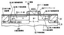
本発明による固体撮像装置においても、その各単位画素におけるセンサー部と、その信号電荷の読み出しMOSトランジスタとは、このMOSトランジスタのソース領域が、センサー部を構成する光電変換領域によって構成される複合構成とする。この構成は、例えば図3にその概略断面図を示すように、例えばSi基板による半導体基板11の、低不純物濃度とされた第1導電型例えばp型の半導体領域上に、それぞれ第2導電型例えばn型の第1および第2半導体領域13および14が、信号電荷の読み出しMOSトランジスタのチャネル長に対応する間隔Lをもって形成される。そして、第1半導体領域13上に、第1導電型、この例ではp型の高不純物濃度層15が形成される。このようにして、p型の高不純物濃度層15と、n型の第1半導体領域13と、p型の半導体領域14とによるp++/n/pによるいわゆるHAD(Hole Accumulated Diode)型のフォトダイオードPD(例えば図1および図2におけるフォトダイオード102もしくは202)、すなわち光電変換領域20が形成される。Also in the solid-state imaging device according to the present invention, the sensor unit in each unit pixel and the signal charge readout MOS transistor are a composite configuration in which the source region of the MOS transistor is constituted by a photoelectric conversion region constituting the sensor unit And For example, as shown in a schematic cross-sectional view in FIG. 3, the second conductivity type is formed on the first conductivity type, for example, the p-type semiconductor region of the semiconductor substrate 11 made of, for example, a Si substrate having a low impurity concentration. For example, the n-type first and
一方、第2半導体領域14上には、これと同導電型の高不純物濃度16が形成される。そして、第1および第2半導体領域13および14間上に、例えば半導体基板11の表面が熱酸化されて形成されたSiO2によるゲート絶縁膜17が形成され、この上に例えば多結晶Siによるゲート電極18が形成されてMOSトランジスタのゲート部が構成される。各高不純物濃度層15および16は、ゲート部に対して、所要の距離例えば0.05μm〜0.2μmの間隔をもって形成される。このため、例えば第1および第2半導体領域13および14は、例えばゲート電極18と、このゲート電極18のパターンエッチングで用いたレジスト層(図示せず)とをマスクとして不純物のイオン注入によって形成し、その後、ゲート電極18の側面にサイドウオール19を形成して、このサイドウオール19と、ゲート電極18とをマスクとして、順次各高不純物濃度層15と16とを、それぞれイオン注入によって形成する。On the other hand, a high impurity concentration 16 of the same conductivity type is formed on the
このようにして、フォトダイオードPDのn型の第1半導体領域13をソース領域とし、n型第2半導体領域14をドレイン領域とし、これら間にゲート絶縁膜17を介してゲート電極18が形成された電荷読み出しのMOSトランジスタ(MOS)が構成される。 In this manner, the n-type
半導体基体11の表面の、センサー部SおよびトランジスタMOSの形成部等の外周の互いに素子分離がなされる部分に、例えば LOCOS(Local Oxidation ofSilicon)によってSiO2による素子分離絶縁層21が形成され、その下に、第1導電型の高濃度のチャネルストップ領域C.Sが形成される。An element
そして、本発明においては、その光電変換領域20に光照射によって発生する信号電荷、この例では電子eに対するポテンシャルが、図4に模式的に示すように、1つの窪みを形成するようになされるように、その形状、パターン等が選定される。一方、MOSトランジスタのゲート電極18、すなわちゲート部は、上述したポテンシャルの窪みの中心部上もしくはその近傍上に延在するパターンおよび位置の選定がなされる。 In the present invention, the signal charge generated by light irradiation in the
このゲート電極18のパターンは、例えば図5A〜Eに例示するように、第1半導体領域13と、第2半導体領域14の互いの対向部、すなわちゲート部のパターンがそのチャネル幅方向に関する中間部において第1半導体領域13に向かって凸の屈曲ないしは湾曲するパターン形状とされて、上述したようにゲート電極18、すなわちゲート部が、上述したポテンシャルの窪みの中心部上もしくはその近傍上に位置することができるようにする。 The pattern of the
このようにゲート電極18、すなわちゲート部が、上述したポテンシャルの窪みの中心部上もしくはその近傍上に位置することができるようにするためには、ゲート電極18の中間部屈曲ないしは湾曲の頂部と、チャネル幅方向の両端との各距離のうち長い方の距離をdとし、上記頂部と光電変換領域20の周縁部の最遠隔距離Dが、距離dの3倍以内(D≦3d)の位置にあるようにする。 Thus, in order to allow the
上述したように、本発明においては、光電変換領域に形成されるポテンシャルの窪みが、単数形成されるようにし、かつ信号電荷の読み出しMOSトランジスタのゲート電極を、このポテンシャルの窪みの中心部、すなわち窪みの頂部、もしくはこの頂部近傍位置にまで延びるように形成したことから、この窪みの周囲の例えば図4で示すチャネルストップ領域C.Sによるポテンシャルバリアの最も高い部分より低い部分から信号電荷の読み出しがなされることから、読み出し電圧を低めることができ、しかもこの信号電荷の読み出しを完全に行うことができる。 As described above, in the present invention, a single potential depression formed in the photoelectric conversion region is formed, and the gate electrode of the signal charge readout MOS transistor is formed at the center of this potential depression, that is, Since it is formed so as to extend to the top of the recess or to a position near the top, for example, the channel stop region C.B shown in FIG. Since the signal charge is read from the lower portion of the potential barrier due to S, the read voltage can be lowered and the signal charge can be completely read.
また、上述したように、表面に高不純物濃度層15を形成するいわゆるHAD構造としたことによって、此処に電荷(信号電荷が電子の場合は正孔)の蓄積層が形成されることから、半導体領域14における信号電荷の蓄積が高められ、かつ暗電流が抑制されることから、MOS型固体撮像装置における固定パターンノイズの改善がはかられるが、この構成において、上述したように、この高不純物濃度層15をゲート部から離間させた構造とすることによって信号電荷の読み出しにおいて、高不純物濃度層15の存在によるポテンシャルバリアの影響を軽減することができ、より完全な読み出しを可能にする。 In addition, as described above, since a so-called HAD structure in which the high impurity concentration layer 15 is formed on the surface, an accumulation layer of charges (holes when signal charges are electrons) is formed here, so that the semiconductor Since the accumulation of signal charges in the
尚、上述した例では、MOSトランジスタが、SiO2ゲート絶縁膜による構成とした場合であるが、このゲート絶縁膜は酸化膜に限定されるものではなく、各種絶縁ゲートトランジスタ構成とすることができる。In the above-described example, the MOS transistor is configured by the SiO2 gate insulating film. However, the gate insulating film is not limited to the oxide film, and various insulating gate transistor configurations can be employed. .
また、通常、固体撮像装置における信号電荷は、電子であるが、信号電荷を正孔とする場合においては、上述した各例において、第1導電型をn型、第2導電型をp型に選定することができるなど、本発明は上述した例に限られるものではなく種々の変更を行うことができる。 In general, the signal charge in the solid-state imaging device is an electron. However, in the case where the signal charge is a hole, in each example described above, the first conductivity type is n-type and the second conductivity type is p-type. The present invention is not limited to the example described above, and various modifications can be made.
S・・・センサー部、MOS・・・MOSトランジスタ、11・・・半導体基板、12・・・半導体領域、13・・・第1半導体領域、14・・・第2半導体領域、4・・・ゲート絶縁膜、15・・・高不純物濃度層、16・・・高不純物濃度層、17・・・ゲート絶縁膜、18・・・ゲート電極、20・・・光電変換領域、101,201・・・単位画素、102,202・・・フォトダイオード、103,203・・・読み出しMOSトランジスタDESCRIPTION OF SYMBOLS S ... Sensor part, MOS ... MOS transistor, 11 ... Semiconductor substrate, 12 ... Semiconductor region, 13 ... 1st semiconductor region, 14 ... 2nd semiconductor region, 4 ... Gate insulating film, 15 ... High impurity concentration layer, 16 ... High impurity concentration layer, 17 ... Gate insulating film, 18 ... Gate electrode, 20 ... Photoelectric conversion region, 101, 201 ... Unit pixel, 102, 202 ... photodiode, 103, 203 ... readout MOS transistor
Claims (2)
Translated fromJapanese上記単位画素は、
第1のN型半導体領域と該N型半導体領域の上部に形成されたP型半導体領域で構成され、光照射により発生した信号電荷を該N型半導体領域に蓄積する光電変換領域と、
上記光電変換領域から上記信号電荷を読み出すMOSトランジスタのゲート電極と、
上記MOSトランジスタのドレイン領域でかつ上記光電変換領域から上記信号電荷を読み出す先である第2のN型半導体領域と、
上記第1のN型半導体領域の外側に配置されたチャネルストップ領域とを有し、
上記ゲート電極は、そのチャネル幅方向に関する上記ゲート電極の中間部において、上記第1のN型半導体領域に向かって凸の屈曲ないしは湾曲パターンで形成される
ことを特徴とする固体撮像装置。A solid-state imaging device including a plurality of unit pixels,
The unit pixel is
A first N-type semiconductor region and a P-type semiconductor region formed above the N-type semiconductor region, and a photoelectric conversion region for accumulating signal charges generated by light irradiation in the N-type semiconductor region;
A gate electrode of a MOS transistor for reading out the signal charge from the photoelectric conversion region;
A second N-type semiconductor region that is a drain region of the MOS transistor and is a destination to read the signal charge from the photoelectric conversion region;
A channel stop region disposed outside the first N-type semiconductor region,
The gate electrode is formed in a convex or curved pattern toward the first N-type semiconductor region at an intermediate portion of the gate electrode in the channel width direction.
Priority Applications (1)
| Application Number | Priority Date | Filing Date | Title |
|---|---|---|---|
| JP2014079699AJP2014135515A (en) | 2014-04-08 | 2014-04-08 | Solid state image pickup device |
Applications Claiming Priority (1)
| Application Number | Priority Date | Filing Date | Title |
|---|---|---|---|
| JP2014079699AJP2014135515A (en) | 2014-04-08 | 2014-04-08 | Solid state image pickup device |
Related Parent Applications (1)
| Application Number | Title | Priority Date | Filing Date |
|---|---|---|---|
| JP2011083064ADivisionJP2011142344A (en) | 2011-04-04 | 2011-04-04 | Solid-state imaging device |
Publications (1)
| Publication Number | Publication Date |
|---|---|
| JP2014135515Atrue JP2014135515A (en) | 2014-07-24 |
Family
ID=51413537
Family Applications (1)
| Application Number | Title | Priority Date | Filing Date |
|---|---|---|---|
| JP2014079699APendingJP2014135515A (en) | 2014-04-08 | 2014-04-08 | Solid state image pickup device |
Country Status (1)
| Country | Link |
|---|---|
| JP (1) | JP2014135515A (en) |
Cited By (1)
| Publication number | Priority date | Publication date | Assignee | Title |
|---|---|---|---|---|
| JP2017054947A (en)* | 2015-09-10 | 2017-03-16 | セイコーエプソン株式会社 | Solid-state imaging device, manufacturing method thereof, and electronic device |
Citations (4)
| Publication number | Priority date | Publication date | Assignee | Title |
|---|---|---|---|---|
| US4148048A (en)* | 1977-01-24 | 1979-04-03 | Hitachi, Ltd. | Solid-state imaging device |
| JPS5815280A (en)* | 1981-07-21 | 1983-01-28 | Nec Corp | solid-state image sensor |
| JPH0230183A (en)* | 1988-07-19 | 1990-01-31 | Nec Corp | Solid-state image sensing element |
| JPH11274462A (en)* | 1998-03-23 | 1999-10-08 | Sony Corp | Solid-state imaging device |
- 2014
- 2014-04-08JPJP2014079699Apatent/JP2014135515A/enactivePending
Patent Citations (4)
| Publication number | Priority date | Publication date | Assignee | Title |
|---|---|---|---|---|
| US4148048A (en)* | 1977-01-24 | 1979-04-03 | Hitachi, Ltd. | Solid-state imaging device |
| JPS5815280A (en)* | 1981-07-21 | 1983-01-28 | Nec Corp | solid-state image sensor |
| JPH0230183A (en)* | 1988-07-19 | 1990-01-31 | Nec Corp | Solid-state image sensing element |
| JPH11274462A (en)* | 1998-03-23 | 1999-10-08 | Sony Corp | Solid-state imaging device |
Cited By (1)
| Publication number | Priority date | Publication date | Assignee | Title |
|---|---|---|---|---|
| JP2017054947A (en)* | 2015-09-10 | 2017-03-16 | セイコーエプソン株式会社 | Solid-state imaging device, manufacturing method thereof, and electronic device |
Similar Documents
| Publication | Publication Date | Title |
|---|---|---|
| JP6541080B2 (en) | Solid-state imaging device | |
| JP4224036B2 (en) | Image sensor with embedded photodiode region and method of manufacturing the same | |
| KR101109088B1 (en) | Solid-state image sensor | |
| JP6406585B2 (en) | Imaging device | |
| JP2009135319A (en) | Solid-state imaging device and camera | |
| JPWO2013094430A1 (en) | Solid-state imaging device, method for manufacturing solid-state imaging device, and electronic apparatus | |
| JP4742602B2 (en) | Solid-state imaging device and manufacturing method thereof | |
| JP2008166607A (en) | Solid-state imaging apparatus, its manufacturing method, semiconductor device and its manufacturing method | |
| KR100605436B1 (en) | Solid-state imaging device | |
| TW201310628A (en) | Solid-state imaging device, method of manufacturing solid-state imaging device, and electronic device | |
| WO2021117523A1 (en) | Solid-state image sensor and electronic device | |
| JP2006253316A (en) | Solid-state imaging device | |
| JPH11274461A (en) | Solid image pickup device and its manufacture | |
| CN105575986A (en) | Solid-state imaging device and method of manufacturing solid-state imaging device | |
| JP2005317875A (en) | Solid-state imaging device | |
| JP2017152481A (en) | Pixel unit and image pick-up device | |
| CN116250248A (en) | Solid-state image pickup device, method of manufacturing the same, and electronic apparatus | |
| JP5581698B2 (en) | Solid-state image sensor | |
| JP2014135515A (en) | Solid state image pickup device | |
| JP2015012240A (en) | Image sensor and electronic device | |
| JP2007134639A (en) | Photoelectric conversion device and imaging device using the same | |
| JP4857816B2 (en) | Solid-state image sensor | |
| JP2011142344A (en) | Solid-state imaging device | |
| JP5487734B2 (en) | Solid-state image sensor | |
| US20250016471A1 (en) | Imaging device |
Legal Events
| Date | Code | Title | Description |
|---|---|---|---|
| A621 | Written request for application examination | Free format text:JAPANESE INTERMEDIATE CODE: A621 Effective date:20140416 | |
| A131 | Notification of reasons for refusal | Free format text:JAPANESE INTERMEDIATE CODE: A131 Effective date:20141111 | |
| A521 | Request for written amendment filed | Free format text:JAPANESE INTERMEDIATE CODE: A523 Effective date:20150107 | |
| A02 | Decision of refusal | Free format text:JAPANESE INTERMEDIATE CODE: A02 Effective date:20150825 |