JP2014135495A - Semiconductor device - Google Patents
Semiconductor deviceDownload PDFInfo
- Publication number
- JP2014135495A JP2014135495AJP2014029187AJP2014029187AJP2014135495AJP 2014135495 AJP2014135495 AJP 2014135495AJP 2014029187 AJP2014029187 AJP 2014029187AJP 2014029187 AJP2014029187 AJP 2014029187AJP 2014135495 AJP2014135495 AJP 2014135495A
- Authority
- JP
- Japan
- Prior art keywords
- thin film
- layer
- film transistor
- oxide semiconductor
- conductive
- Prior art date
- Legal status (The legal status is an assumption and is not a legal conclusion. Google has not performed a legal analysis and makes no representation as to the accuracy of the status listed.)
- Granted
Links
Images


Classifications
- H—ELECTRICITY
- H10—SEMICONDUCTOR DEVICES; ELECTRIC SOLID-STATE DEVICES NOT OTHERWISE PROVIDED FOR
- H10D—INORGANIC ELECTRIC SEMICONDUCTOR DEVICES
- H10D64/00—Electrodes of devices having potential barriers
- H10D64/60—Electrodes characterised by their materials
- H10D64/62—Electrodes ohmically coupled to a semiconductor
- H—ELECTRICITY
- H10—SEMICONDUCTOR DEVICES; ELECTRIC SOLID-STATE DEVICES NOT OTHERWISE PROVIDED FOR
- H10D—INORGANIC ELECTRIC SEMICONDUCTOR DEVICES
- H10D30/00—Field-effect transistors [FET]
- H10D30/01—Manufacture or treatment
- H10D30/021—Manufacture or treatment of FETs having insulated gates [IGFET]
- H10D30/031—Manufacture or treatment of FETs having insulated gates [IGFET] of thin-film transistors [TFT]
- H—ELECTRICITY
- H10—SEMICONDUCTOR DEVICES; ELECTRIC SOLID-STATE DEVICES NOT OTHERWISE PROVIDED FOR
- H10D—INORGANIC ELECTRIC SEMICONDUCTOR DEVICES
- H10D30/00—Field-effect transistors [FET]
- H10D30/60—Insulated-gate field-effect transistors [IGFET]
- H10D30/67—Thin-film transistors [TFT]
- H10D30/6704—Thin-film transistors [TFT] having supplementary regions or layers in the thin films or in the insulated bulk substrates for controlling properties of the device
- H—ELECTRICITY
- H10—SEMICONDUCTOR DEVICES; ELECTRIC SOLID-STATE DEVICES NOT OTHERWISE PROVIDED FOR
- H10D—INORGANIC ELECTRIC SEMICONDUCTOR DEVICES
- H10D30/00—Field-effect transistors [FET]
- H10D30/60—Insulated-gate field-effect transistors [IGFET]
- H10D30/67—Thin-film transistors [TFT]
- H10D30/674—Thin-film transistors [TFT] characterised by the active materials
- H10D30/6755—Oxide semiconductors, e.g. zinc oxide, copper aluminium oxide or cadmium stannate
- H—ELECTRICITY
- H10—SEMICONDUCTOR DEVICES; ELECTRIC SOLID-STATE DEVICES NOT OTHERWISE PROVIDED FOR
- H10D—INORGANIC ELECTRIC SEMICONDUCTOR DEVICES
- H10D86/00—Integrated devices formed in or on insulating or conducting substrates, e.g. formed in silicon-on-insulator [SOI] substrates or on stainless steel or glass substrates
- H10D86/40—Integrated devices formed in or on insulating or conducting substrates, e.g. formed in silicon-on-insulator [SOI] substrates or on stainless steel or glass substrates characterised by multiple TFTs
- H10D86/60—Integrated devices formed in or on insulating or conducting substrates, e.g. formed in silicon-on-insulator [SOI] substrates or on stainless steel or glass substrates characterised by multiple TFTs wherein the TFTs are in active matrices
- H—ELECTRICITY
- H10—SEMICONDUCTOR DEVICES; ELECTRIC SOLID-STATE DEVICES NOT OTHERWISE PROVIDED FOR
- H10D—INORGANIC ELECTRIC SEMICONDUCTOR DEVICES
- H10D86/00—Integrated devices formed in or on insulating or conducting substrates, e.g. formed in silicon-on-insulator [SOI] substrates or on stainless steel or glass substrates
- H10D86/40—Integrated devices formed in or on insulating or conducting substrates, e.g. formed in silicon-on-insulator [SOI] substrates or on stainless steel or glass substrates characterised by multiple TFTs
- H10D86/421—Integrated devices formed in or on insulating or conducting substrates, e.g. formed in silicon-on-insulator [SOI] substrates or on stainless steel or glass substrates characterised by multiple TFTs having a particular composition, shape or crystalline structure of the active layer
- H10D86/423—Integrated devices formed in or on insulating or conducting substrates, e.g. formed in silicon-on-insulator [SOI] substrates or on stainless steel or glass substrates characterised by multiple TFTs having a particular composition, shape or crystalline structure of the active layer comprising semiconductor materials not belonging to the Group IV, e.g. InGaZnO
Landscapes
- Thin Film Transistor (AREA)
- Electrodes Of Semiconductors (AREA)
- Devices For Indicating Variable Information By Combining Individual Elements (AREA)
- Electroluminescent Light Sources (AREA)
Abstract
Translated fromJapaneseDescription
Translated fromJapanese本発明の一態様はチャネル形成領域に酸化物半導体膜を用いた薄膜トランジスタ(以下、
TFTという)で構成された回路を有する半導体装置およびその作製方法に関する。例え
ば、液晶表示パネルに代表される電気光学装置や有機発光素子を有する発光表示装置を部
品として搭載した電子機器に関する。
なお、本明細書中において半導体装置とは、半導体特性を利用することで機能しうる装置
全般を指し、電気光学装置、半導体回路および電子機器は全て半導体装置である。One embodiment of the present invention is a thin film transistor using an oxide semiconductor film in a channel formation region (hereinafter referred to as a thin film transistor).
The present invention relates to a semiconductor device having a circuit including a TFT and a manufacturing method thereof. For example, the present invention relates to an electronic apparatus in which an electro-optical device typified by a liquid crystal display panel or a light-emitting display device having an organic light-emitting element is mounted as a component.
Note that in this specification, a semiconductor device refers to all devices that can function by utilizing semiconductor characteristics, and an electro-optical device, a semiconductor circuit, and an electronic device are all semiconductor devices.
近年、マトリクス状に配置された表示画素毎に薄膜トランジスタ(TFT)からなるスイ
ッチング素子を設けたアクティブマトリクス型の表示装置(液晶表示装置や発光表示装置
や電気泳動式表示装置)が盛んに開発されている。アクティブマトリクス型の表示装置は
、画素(又は1ドット)毎にスイッチング素子が設けられており、単純マトリクス方式に
比べて画素密度が増えた場合に低電圧駆動できるので有利である。In recent years, active matrix display devices (liquid crystal display devices, light-emitting display devices, and electrophoretic display devices) in which switching elements made of thin film transistors (TFTs) are provided for each display pixel arranged in a matrix have been actively developed. Yes. An active matrix display device is advantageous in that a switching element is provided for each pixel (or one dot) and can be driven at a low voltage when the pixel density is increased as compared with the simple matrix method.
また、チャネル形成領域に酸化物半導体膜を用いて薄膜トランジスタ(TFT)などを作
製し、電子デバイスや光デバイスに応用する技術が注目されている。例えば、酸化物半導
体膜としてZnOを用いる薄膜トランジスタや、インジウム、ガリウム、及び亜鉛を含む
酸化物を用いる薄膜トランジスタをその例に挙げることができる。これらの酸化物半導体
膜を用いた薄膜トランジスタを透光性を有する基板上に形成し、画像表示装置のスイッチ
ング素子などに用いる技術が特許文献1、特許文献2などで開示されている。In addition, a technique in which a thin film transistor (TFT) or the like is manufactured using an oxide semiconductor film in a channel formation region and applied to an electronic device or an optical device has attracted attention. For example, a thin film transistor using ZnO as an oxide semiconductor film or a thin film transistor using an oxide containing indium, gallium, and zinc can be given as examples. A technique in which a thin film transistor using such an oxide semiconductor film is formed over a light-transmitting substrate and used as a switching element of an image display device is disclosed in
また、種々の導電層が酸化物半導体を用いた薄膜トランジスタのソース電極層及びドレイ
ン電極層に用いられている。例えば、金属膜としてチタンと白金の積層膜(非特許文献1
)、透光性を有する導電膜としてインジウム(In)と亜鉛(Zn)を含む酸化物(非特
許文献2)、金属膜と透光性を有する導電膜の積層膜としてインジウム錫酸化物と金の積
層膜が(非特許文献3)が知られている。In addition, various conductive layers are used for a source electrode layer and a drain electrode layer of a thin film transistor using an oxide semiconductor. For example, a laminated film of titanium and platinum as a metal film (Non-Patent Document 1)
), An oxide containing indium (In) and zinc (Zn) as a light-transmitting conductive film (Non-patent Document 2), and a stacked film of a metal film and a light-transmitting conductive film as indium tin oxide and gold (Non-patent Document 3) is known.
一方、アルミニウム膜は導電性と加工性に優れており、また安価であるため、半導体素子
の配線材料への応用が盛んである。しかし、アルミニウム原子は拡散し易いため、単にア
ルミニウム膜を配線材料に用いると、ヒロック、エレクトロマイグレーション、ストレス
マイグレーションなど、アルミニウム原子の拡散に伴う不具合が生ずることが知られてい
る。特に、半導体素子の作製工程における熱処理は、アルミニウム原子の拡散を促進して
しまう。On the other hand, an aluminum film is excellent in conductivity and workability, and is inexpensive, so that it is actively applied to a wiring material for semiconductor elements. However, since aluminum atoms are easily diffused, it is known that if an aluminum film is simply used as a wiring material, problems associated with diffusion of aluminum atoms such as hillocks, electromigration, and stress migration occur. In particular, the heat treatment in the manufacturing process of the semiconductor element promotes diffusion of aluminum atoms.
そこで、アルミニウム原子の拡散を抑制するために、不純物を添加する方法や、タングス
テンやモリブデン等の高融点の金属材料を積層する方法が知られている。特に、隣接する
層との間に高融点の金属材料を挟む構造は、アルミニウム原子の拡散を抑制する手段とし
て有効である。このような高融点の金属材料の層はバリアメタル層と呼ばれている。Therefore, in order to suppress diffusion of aluminum atoms, a method of adding impurities and a method of laminating a high melting point metal material such as tungsten or molybdenum are known. In particular, a structure in which a metal material having a high melting point is sandwiched between adjacent layers is effective as a means for suppressing diffusion of aluminum atoms. Such a layer of a refractory metal material is called a barrier metal layer.
チャネル形成領域にインジウム、ガリウム、及び亜鉛を含む酸化物半導体膜を用いる薄膜
トランジスタには、動作速度が速く、製造工程が比較的簡単であり、十分な信頼性である
ことが求められている。しかし、薄膜トランジスタの電気特性や信頼性はチャネル領域に
不純物元素が拡散することで損なわれてしまうことがある。A thin film transistor using an oxide semiconductor film containing indium, gallium, and zinc in a channel formation region is required to have a high operation speed, a relatively simple manufacturing process, and sufficient reliability. However, the electrical characteristics and reliability of the thin film transistor may be impaired by the diffusion of the impurity element into the channel region.
アルミニウムを主成分とする第1導電膜をソース電極層及びドレイン電極層に用いる場合
、第1導電膜とチャネル領域を形成する半導体層の間に高融点の金属材料からなる第2導
電膜を挟み込む構造にすれば、第2導電膜がバリア層として働き、アルミニウム原子がチ
ャネル領域に拡散する現象を防ぐことができる。When the first conductive film containing aluminum as a main component is used for the source electrode layer and the drain electrode layer, the second conductive film made of a metal material with a high melting point is sandwiched between the first conductive film and the semiconductor layer forming the channel region. With this structure, the second conductive film functions as a barrier layer, and the phenomenon that aluminum atoms diffuse into the channel region can be prevented.
しかし、アルミニウムを主成分とする第1導電膜と高融点の金属材料からなる第2導電膜
の積層導電膜をエッチングしてソース電極層及びドレイン電極層を形成した場合、その端
部にはアルミニウムを第1成分とする第1導電層が露出してしまう。このソース電極層及
びドレイン電極層に酸化物半導体膜を積層すれば、端部に露出したアルミニウムを主成分
とした第1導電層と酸化物半導体膜が直に接触してしまう。また、アルミニウムを第1成
分とする第1導電層がチャネル領域を挟む構造になってしまう。この結果、アルミニウム
を主成分とした第1導電層の端部からインジウム、ガリウム、及び亜鉛を含む酸化物半導
体膜へアルミニウム原子が拡散し易くなるという問題が生じる。However, when the source electrode layer and the drain electrode layer are formed by etching the stacked conductive film of the first conductive film containing aluminum as a main component and the second conductive film made of a metal material having a high melting point, aluminum is formed at the end portion. As a result, the first conductive layer having the first component is exposed. When an oxide semiconductor film is stacked on the source electrode layer and the drain electrode layer, the first conductive layer mainly composed of aluminum exposed at the end and the oxide semiconductor film are in direct contact with each other. Further, the first conductive layer containing aluminum as the first component sandwiches the channel region. As a result, there arises a problem that aluminum atoms are easily diffused from an end portion of the first conductive layer containing aluminum as a main component into an oxide semiconductor film containing indium, gallium, and zinc.
また、インジウム、ガリウム、及び亜鉛を含む酸化物半導体を用いた半導体素子は、熱処
理により薄膜トランジスタ特性が改善する。(具体的には、オン電流が大きくなり、トラ
ンジスタ特性のバラツキが減少する。)そのため、インジウム、ガリウム、及び亜鉛を含
む酸化物半導体膜は形成後に熱処理を施すことが好ましいが、熱処理はアルミニウムを第
1成分とする第1導電層から酸化物半導体層へアルミニウム原子が熱拡散する現象を促進
してしまう。In addition, in a semiconductor element using an oxide semiconductor containing indium, gallium, and zinc, thin film transistor characteristics are improved by heat treatment. (Specifically, the on-state current is increased and the variation in transistor characteristics is reduced.) Therefore, it is preferable that the oxide semiconductor film containing indium, gallium, and zinc be subjected to heat treatment after formation. The phenomenon that aluminum atoms thermally diffuse from the first conductive layer as the first component to the oxide semiconductor layer is promoted.
本発明の一態様では、アルミニウムを第1成分とする第1導電層を有するソース電極層及
びドレイン電極層上にインジウム、ガリウム、及び亜鉛を含む酸化物半導体膜を積層した
薄膜トランジスタにおいて、前記第1導電層からアルミニウム原子が前記酸化物半導体層
へ拡散し難い薄膜トランジスタを提供することを課題とする。In one embodiment of the present invention, in the thin film transistor in which the oxide semiconductor film containing indium, gallium, and zinc is stacked over the source electrode layer and the drain electrode layer each including the first conductive layer containing aluminum as the first component, It is an object to provide a thin film transistor in which aluminum atoms are unlikely to diffuse from the conductive layer to the oxide semiconductor layer.
また、アルミニウムを第1成分とする第1導電層を有するソース電極層及びドレイン電極
層上にインジウム、ガリウム、及び亜鉛を含む酸化物半導体膜を積層した薄膜トランジス
タにおいて、前記第1導電層からアルミニウム原子が前記酸化物半導体層へ拡散し難い薄
膜トランジスタの作製方法を提供することを課題とする。In the thin film transistor in which an oxide semiconductor film containing indium, gallium, and zinc is stacked over a source electrode layer and a drain electrode layer having a first conductive layer containing aluminum as a first component, an aluminum atom is formed from the first conductive layer. It is an object of the present invention to provide a method for manufacturing a thin film transistor which is difficult to diffuse into the oxide semiconductor layer.
本発明の一態様は、アルミニウムを第1成分とする第1導電層からアルミニウム原子がイ
ンジウム、ガリウム、及び亜鉛を含む酸化物半導体膜に拡散するのを防ぐためにバリア層
を設けた半導体装置およびその作成方法であり、ソース電極層及びドレイン電極層の端部
において、酸化処理されたアルミニウムを主成分とする層とインジウム、ガリウム、及び
亜鉛を含む酸化物半導体層が接する半導体装置およびその作製方法を含むことを要旨とす
る。One embodiment of the present invention is a semiconductor device provided with a barrier layer for preventing aluminum atoms from diffusing from an oxide semiconductor film containing indium, gallium, and zinc from a first conductive layer containing aluminum as a first component, and a semiconductor device thereof A method of manufacturing a semiconductor device in which an oxidized aluminum layer and an oxide semiconductor layer containing indium, gallium, and zinc are in contact with each other at an end portion of a source electrode layer and a drain electrode layer. Inclusion is included.
具体的には、導電層の端部に現れるアルミニウムを第1成分とする第1導電層を、意図的
に酸化してバリア層を形成する。なお、バリア層の膜厚は0より大で5nm以下であり、
緻密な非水和酸化アルミニウムを主成分とする。Specifically, the barrier layer is formed by intentionally oxidizing the first conductive layer containing aluminum that appears at the end of the conductive layer as the first component. Note that the thickness of the barrier layer is greater than 0 and 5 nm or less,
Mainly dense non-hydrated aluminum oxide.
本発明の一態様は、インジウム、ガリウム、及び亜鉛を含む酸化物半導体層と、アルミニ
ウムを第1成分とする第1導電層と、高融点金属材料からなる第2導電層と、酸化アルミ
ニウムを第1成分とするバリア層を有し、第1導電層上に第2導電層が積層され、第1導
電層の端部にバリア層が形成され、酸化物半導体層が第2導電層又は前記バリア層と接し
て設けられた半導体装置である。One embodiment of the present invention is an oxide semiconductor layer containing indium, gallium, and zinc, a first conductive layer containing aluminum as a first component, a second conductive layer made of a refractory metal material, and aluminum oxide The barrier layer is a single component, the second conductive layer is stacked on the first conductive layer, the barrier layer is formed at the end of the first conductive layer, and the oxide semiconductor layer is the second conductive layer or the barrier. A semiconductor device is provided in contact with a layer.
また、ゲート絶縁層と、ゲート絶縁層の一方の側に設けられたゲート電極層と、ゲート絶
縁層の他方の側に設けられた酸化物半導体層と、ゲート絶縁層に接しアルミニウムを第1
成分とする第1導電層と、第一導電層上に高融点金属材料からなる第2導電層が積層され
、第1導電層の端部に酸化アルミニウムを第1成分とするバリア層が設けられたソース電
極層及びドレイン電極層とを有し、酸化物半導体層が、第2導電層およびバリア層と接す
ることを特徴とする半導体装置である。A gate insulating layer; a gate electrode layer provided on one side of the gate insulating layer; an oxide semiconductor layer provided on the other side of the gate insulating layer;
A first conductive layer as a component and a second conductive layer made of a refractory metal material are stacked on the first conductive layer, and a barrier layer containing aluminum oxide as a first component is provided at the end of the first conductive layer. And a source electrode layer and a drain electrode layer, wherein the oxide semiconductor layer is in contact with the second conductive layer and the barrier layer.
また、アルミニウムを第1成分とする第1導電層と、第1導電層上に高融点金属材料から
なる第2導電層が積層され、第1導電層の端部に酸化アルミニウムを第1成分とするバリ
ア層が設けられたソース電極層及びドレイン電極層と、ソース電極層及びドレイン電極層
の端部を覆う酸化物半導体層と、酸化物半導体層を覆うゲート絶縁層と、酸化物半導体層
とゲート絶縁層を介してソース電極層及びドレイン電極層の端部に重畳するゲート電極層
とを有し、酸化物半導体層が、第2導電層およびバリア層と接することを特徴とする半導
体装置。In addition, a first conductive layer containing aluminum as a first component and a second conductive layer made of a refractory metal material are stacked on the first conductive layer, and aluminum oxide is formed on the end of the first conductive layer as a first component. A source electrode layer and a drain electrode layer provided with a barrier layer, an oxide semiconductor layer covering end portions of the source electrode layer and the drain electrode layer, a gate insulating layer covering the oxide semiconductor layer, an oxide semiconductor layer, And a gate electrode layer overlapping with end portions of the source electrode layer and the drain electrode layer with the gate insulating layer interposed therebetween, and the oxide semiconductor layer is in contact with the second conductive layer and the barrier layer.
また、上記酸化アルミニウムを第1成分とするバリア層の厚さが0より大で5nm以下で
あることを特徴とする半導体装置である。In the semiconductor device, the thickness of the barrier layer containing aluminum oxide as a first component is greater than 0 and equal to or less than 5 nm.
また、アルミニウムを第1成分とする第1導電層上に高融点金属材料からなる第2導電層
を積層したソース電極層及びドレイン電極層を形成し、前記ソース電極層及びドレイン電
極層の端部に露出した前記第1導電層を酸化処理して酸化アルミニウムを第1成分とする
バリア層を形成し、前記第2導電層および前記バリア層と接して、インジウム、ガリウム
、及び亜鉛を含む酸化物半導体層を積層することを特徴とする薄膜トランジスタの作成方
法である。Further, a source electrode layer and a drain electrode layer are formed by laminating a second conductive layer made of a refractory metal material on a first conductive layer containing aluminum as a first component, and end portions of the source electrode layer and the drain electrode layer are formed. An oxide containing indium, gallium, and zinc in contact with the second conductive layer and the barrier layer is formed by oxidizing the first conductive layer exposed to the surface to form a barrier layer containing aluminum oxide as a first component. A thin film transistor is formed by stacking semiconductor layers.
本発明の一態様により、インジウム、ガリウム、及び亜鉛を含む酸化物半導体層とアルミ
ニウムを主成分とする第1導電層との間に高融点の金属材料からなる第2導電層もしくは
酸化アルミニウムを第1成分とするバリア層を形成するため、アルミニウム原子の酸化物
半導体層への拡散を抑制できる。特に、インジウム、ガリウム、及び亜鉛を含む酸化物半
導体層を熱処理しても、アルミニウム原子の酸化物半導体層への拡散を抑制できる。また
、インジウム、ガリウム、及び亜鉛を含む酸化物半導体層とアルミニウムを第1成分とす
る第1導電層との間で生じる電食(電気化学的腐食ともいう)を防ぐことができる。よっ
て、信頼性のよい薄膜トランジスタを有する半導体装置を提供できる。According to one embodiment of the present invention, a second conductive layer or an aluminum oxide formed of a metal material with a high melting point is provided between an oxide semiconductor layer containing indium, gallium, and zinc and a first conductive layer containing aluminum as a main component. Since the barrier layer having one component is formed, diffusion of aluminum atoms into the oxide semiconductor layer can be suppressed. In particular, even when heat treatment is performed on an oxide semiconductor layer containing indium, gallium, and zinc, diffusion of aluminum atoms into the oxide semiconductor layer can be suppressed. In addition, electrolytic corrosion (also referred to as electrochemical corrosion) that occurs between the oxide semiconductor layer containing indium, gallium, and zinc and the first conductive layer containing aluminum as a first component can be prevented. Thus, a semiconductor device including a highly reliable thin film transistor can be provided.
以下では、本発明の実施の形態について図面を用いて詳細に説明する。ただし、本発明は
以下の説明に限定されず、本発明の趣旨およびその範囲から逸脱することなくその形態お
よび詳細を様々に変更し得ることは、当業者であれば容易に理解される。したがって、本
発明は以下に示す実施の形態の記載内容に限定して解釈されるものではない。なお、以下
に説明する本発明の構成において、同一部分又は同様な機能を有する部分には同一の符号
を異なる図面間で共通して用い、その繰り返しの説明は省略する。Hereinafter, embodiments of the present invention will be described in detail with reference to the drawings. However, the present invention is not limited to the following description, and it is easily understood by those skilled in the art that modes and details can be variously changed without departing from the spirit and scope of the present invention. Therefore, the present invention should not be construed as being limited to the description of the embodiments below. Note that in structures of the present invention described below, the same portions or portions having similar functions are denoted by the same reference numerals in different drawings, and description thereof is not repeated.
(実施の形態1)
本実施の形態では、薄膜トランジスタおよびその作製工程について、図1乃至図3を用い
て説明する。(Embodiment 1)
In this embodiment, a thin film transistor and a manufacturing process thereof will be described with reference to FIGS.
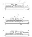
図1には、本実施の形態の薄膜トランジスタを示す。図1(A)は平面図であり、図1(
B)は図1(A)におけるQ1−Q2で切断した断面図である。図1に示す薄膜トランジ
スタ150は、基板100上にゲート電極層111が形成され、ゲート電極層111上に
ゲート絶縁膜102が形成され、アルミニウムを第1成分とする第1導電層(114a、
114b)上に高融点金属材料によって形成される第2導電層(115a、115b)を
積層したソース電極層及びドレイン電極層(117a、117b)が端部をゲート電極層
111に重畳してゲート絶縁膜102上に形成され、ソース電極層及びドレイン電極層の
高融点金属材料によって形成される第2導電層(115a、115b)と、ソース電極層
及びドレイン電極層の端部にある酸化アルミニウムを第1成分とするバリア層(116a
、116b)に接して、酸化物半導体層113がゲート電極層111に重畳して形成され
ている。FIG. 1 shows a thin film transistor of this embodiment mode. FIG. 1A is a plan view, and FIG.
B) is a cross-sectional view taken along Q1-Q2 in FIG. A
114b) The source and drain electrode layers (117a, 117b) in which the second conductive layers (115a, 115b) formed of a refractory metal material are stacked on the
, 116 b), the
酸化物半導体層113はソース電極層及びドレイン電極層の高融点金属材料によって形成
される第2導電層(115a、115b)と、ソース電極層及びドレイン電極層の端部に
ある酸化アルミニウムを第1成分とするバリア層(116a、116b)に接している。The
本実施の形態では、アルミニウムを第1成分とする第1導電層(114a、114b)と
高融点の金属材料からなる第2導電層(115a、115b)を積層したソース電極層及
びドレイン電極層(117a、117b)の端部に酸化アルミニウムを第1成分とするバ
リア層(116a、116b)を形成する。そのため酸化物半導体とアルミニウムを第1
成分とする第1導電層は互いに直接ふれていない。In this embodiment, a source electrode layer and a drain electrode layer (115a, 115b) in which a first conductive layer (114a, 114b) containing aluminum as a first component and a second conductive layer (115a, 115b) made of a high melting point metal material are stacked. Barrier layers (116a, 116b) containing aluminum oxide as a first component are formed at the ends of 117a, 117b). Therefore, the oxide semiconductor and aluminum are the first.
The first conductive layers as components do not touch each other directly.
本明細書中で酸化物半導体層に用いる酸化物半導体は、InMO3(ZnO)m(m>0
)で表記される薄膜を形成し、その薄膜を半導体層として用いた薄膜トランジスタを作製
する。なお、Mは、Ga、Fe、Ni、Mn及びCoから選ばれた一の金属元素又は複数
の金属元素を示す。例えばMとして、Gaの場合があることの他、GaとNi又はGaと
Feなど、Ga以外の上記金属元素が含まれる場合がある。また、上記酸化物半導体にお
いて、Mとして含まれる金属元素の他に、不純物元素としてFe、Niその他の遷移金属
元素、又は該遷移金属の酸化物が含まれているものがある。本明細書においてはこの薄膜
をIn−Ga−Zn−O系非単結晶膜とも呼ぶ。In this specification, the oxide semiconductor used for the oxide semiconductor layer is InMO3 (ZnO)m (m> 0
) Is formed, and a thin film transistor using the thin film as a semiconductor layer is manufactured. Note that M represents one metal element or a plurality of metal elements selected from Ga, Fe, Ni, Mn, and Co. For example, M may be Ga, and may contain the above metal elements other than Ga, such as Ga and Ni or Ga and Fe. In addition to the metal element contained as M, some of the above oxide semiconductors contain Fe, Ni, other transition metal elements, or oxides of the transition metal as impurity elements. In this specification, this thin film is also referred to as an In—Ga—Zn—O-based non-single-crystal film.
In−Ga−Zn−O系非単結晶膜の組成比は、成膜条件により変化する。ここでは、I
n2O3:Ga2O3:ZnO=1:1:1としたターゲット(組成比として、In:G
a:Zn=1:1:0.5)を用い、スパッタリング法でのアルゴンガス流量を40sc
cmとした条件を条件1とし、スパッタリング法でのアルゴンガス流量を10sccm、
酸素を5sccmとした条件を条件2とする。The composition ratio of the In—Ga—Zn—O-based non-single-crystal film varies depending on deposition conditions. Here I
n2 O3 : Ga2 O3 : ZnO = 1: 1: 1 target (composition ratio: In: G
a: Zn = 1: 1: 0.5), and the argon gas flow rate in the sputtering method is 40 sc.
cm is the
The condition under which oxygen is 5 sccm is defined as
誘導結合プラズマ質量分析法(ICP−MS : Inductively Coupl
ed Plasma Mass Spectrometry)により測定した代表的な酸
化物半導体膜の組成比は、条件1で成膜した場合はInGa0.95Zn0.41O3.
33であり、条件2で成膜した場合は、InGa0.94Zn0.40O3.31である
。Inductively coupled plasma mass spectrometry (ICP-MS: Inductive Couple)
The composition ratio of a typical oxide semiconductor film measured by ed Plasma Mass Spectrometry is InGa0.95 Zn0.41 O when formed under
In the case of film formation under
また、測定方法をラザフォード後方散乱分析法(RBS : Rutherford B
ackscattering Spectrometry)に変えて定量化した代表的な
酸化物半導体膜の組成比は、条件1で成膜した場合はInGa0.93Zn0.44O3
.49であり、条件2で成膜した場合はInGa0.92Zn0.45O3.86である
。The measurement method is Rutherford Backscattering Analysis (RBS).
The composition ratio of a typical oxide semiconductor film quantified in place of ackscattering (spectrometry) is InGa0.93 Zn0.44 O3 when formed under
. 49. In the case where the film is formed under the
In−Ga−Zn−O系非単結晶膜の結晶構造は、スパッタリング法で成膜した後、20
0℃〜500℃、代表的には300〜400℃で10分〜100分の熱処理を行っている
ため、アモルファス構造がX線回折(XRD:X−ray diffraction)の
分析では観察される。The crystal structure of the In—Ga—Zn—O-based non-single-crystal film is 20
Since heat treatment is performed at 0 to 500 ° C., typically 300 to 400 ° C. for 10 to 100 minutes, an amorphous structure is observed in the analysis of X-ray diffraction (XRD).
また、インジウム、ガリウム、及び亜鉛を含む酸化物半導体層は光吸収が少なく光励起さ
れ難いため、チャネル形成領域をゲート電極層で覆って遮光する必要がない。すなわち、
チャネル形成領域において、ゲート電極層とソース電極層及びドレイン電極層の重なりを
減らすことができ、寄生容量を軽減できる。In addition, since the oxide semiconductor layer containing indium, gallium, and zinc has little light absorption and is difficult to be photoexcited, it is not necessary to cover the channel formation region with the gate electrode layer and shield it from light. That is,
In the channel formation region, overlap between the gate electrode layer, the source electrode layer, and the drain electrode layer can be reduced, and parasitic capacitance can be reduced.
図1(A)、(B)の薄膜トランジスタ150の作製方法を図2及び図3を用いて説明す
る。A method for manufacturing the
基板100は、バリウムホウケイ酸ガラス、アルミノホウケイ酸ガラス、若しくはアルミ
ノシリケートガラスなど、フュージョン法やフロート法で作製される無アルカリガラス基
板、セラミック基板の他、本作製工程の処理温度に耐えうる耐熱性を有するプラスチック
基板等を用いることができる。例えば、成分比として酸化ホウ素(B2O3)よりも酸化
バリウム(BaO)を多く含み、歪み点が730℃以上のガラス基板を用いると好ましい
。酸化物半導体層を700℃程度の高温で熱処理する場合でも、ガラス基板が歪まないで
済むからである。また、ステンレス合金などの金属基板の表面に絶縁膜を設けた基板を適
用しても良い。基板100がマザーガラスの場合、基板の大きさは、第1世代(320m
m×400mm)、第2世代(400mm×500mm)、第3世代(550mm×65
0mm)、第4世代(680mm×880mm、または730mm×920mm)、第5
世代(1000mm×1200mmまたは1100mm×1250mm)、第6世代15
00mm×1800mm)、第7世代(1900mm×2200mm)、第8世代(21
60mm×2460mm)、第9世代(2400mm×2800mm、2450mm×3
050mm)、第10世代(2950mm×3400mm)等を用いることができる。The
m × 400 mm), second generation (400 mm × 500 mm), third generation (550 mm × 65)
0 mm), 4th generation (680 mm × 880 mm, or 730 mm × 920 mm), 5th
Generation (1000mm x 1200mm or 1100mm x 1250mm), 6th generation 15
00mm x 1800mm), 7th generation (1900mm x 2200mm), 8th generation (21
60mm x 2460mm), 9th generation (2400mm x 2800mm, 2450mm x 3)
050 mm), 10th generation (2950 mm × 3400 mm), or the like can be used.
また基板100上に下地膜として絶縁膜を形成してもよい。下地膜としては、CVD法や
スパッタリング法等を用いて、酸化珪素膜、窒化珪素膜、酸化窒化珪素膜、または窒化酸
化珪素膜の単層、又は積層で形成すればよい。An insulating film may be formed over the
次に、ゲート電極層111を含むゲート配線と容量配線および端子部となる導電膜を成膜
する。導電膜は、アルミニウム(Al)や銅(Cu)などの低抵抗導電性材料で形成する
ことが望ましいが、Al単体では耐熱性が劣り、また腐蝕しやすい等の問題点があるので
耐熱性導電性材料と組み合わせて形成する。耐熱性導電性材料としては、チタン(Ti)
、タンタル(Ta)、タングステン(W)、モリブデン(Mo)、クロム(Cr)、ネオ
ジム(Nd)、スカンジウム(Sc)から選ばれた元素、または上述した元素を成分とす
る合金か、上述した元素を組み合わせた合金膜、または上述した元素を成分とする窒化物
で形成する。Next, a gate wiring including the
An element selected from tantalum (Ta), tungsten (W), molybdenum (Mo), chromium (Cr), neodymium (Nd), scandium (Sc), or an alloy containing the above elements as a component, or the above elements An alloy film combining these elements or a nitride containing the above-described elements as a component is formed.
また、透明導電膜でもよく、材料としてはインジウム錫酸化物、珪素もしくは酸化珪素を
含有したインジウム錫酸化物、インジウム亜鉛酸化物、酸化亜鉛などを用いることもでき
る。Further, a transparent conductive film may be used, and as the material, indium tin oxide, indium tin oxide containing silicon or silicon oxide, indium zinc oxide, zinc oxide, or the like can be used.
ゲート電極層111となる導電膜は厚さ50nm以上300nm以下で形成する。ゲート
電極層111を含む配線層となる導電膜の厚さを300nm以下とすることで、後に形成
される半導体膜や配線の段切れ防止が可能である。また、ゲート電極層111を含む配線
層となる導電膜の厚さを150nm以上とすることで、ゲート電極の抵抗を低減すること
が可能であり、大面積化が可能である。The conductive film to be the
次いで、本実施の形態における第1のフォトマスクを用いて形成したレジストマスクを使
い、基板上に形成された導電膜の不要な部分をエッチングして除去して配線及び電極(ゲ
ート電極層111を含むゲート配線、容量配線、及び端子)を形成する。このとき少なく
ともゲート電極層111の端部にテーパー形状が形成されるようにエッチングする。この
段階での段面図を図2(A)に示す。Next, using a resist mask formed using the first photomask in this embodiment, unnecessary portions of the conductive film formed over the substrate are removed by etching to remove wirings and electrodes (the
次にゲート絶縁膜102を形成する。ゲート絶縁膜102として利用できる絶縁膜として
は、酸化珪素膜、窒化珪素膜、酸化窒化珪素膜、窒化酸化珪素膜、酸化アルミニウム、酸
化マグネシウム、窒化アルミニウム、酸化イットリウム、酸化ハフニウム、酸化タンタル
膜をその例に挙げることができる。Next, the
ここでは、酸化窒化珪素膜とは、その組成として、窒素よりも酸素の含有量が多いもので
あって、濃度範囲として酸素が55〜65原子%、窒素が1〜20原子%、Siが25〜
35原子%、水素が0.1〜10原子%の範囲で含まれるものをいう。また、窒化酸化珪
素膜とは、その組成として、酸素よりも窒素の含有量が多いものであって、濃度範囲とし
て酸素が15〜30原子%、窒素が20〜35原子%、Siが25〜35原子%、水素が
15〜25原子%の範囲で含まれるものをいう。Here, the silicon oxynitride film has a composition that contains more oxygen than nitrogen and has a concentration range of 55 to 65 atomic%, 1 to 20 atomic%, and 25 Si. ~
35 atomic% and hydrogen are contained in the range of 0.1 to 10 atomic%. The silicon nitride oxide film has a composition containing more nitrogen than oxygen, and the concentration ranges of oxygen are 15 to 30 atomic%, nitrogen is 20 to 35 atomic%, and Si is 25 to 25%. 35 atomic% and hydrogen are included in the range of 15 to 25 atomic%.
ゲート絶縁膜は単層であっても、絶縁膜を2層または3層積層して形成してもよい。例え
ば、基板に接するゲート絶縁膜を窒化珪素膜、または窒化酸化珪素膜を用いて形成するこ
とで、基板とゲート絶縁膜の密着力が高まり、基板としてガラス基板を用いた場合、基板
からの不純物が酸化物半導体層113に拡散するのを防止することが可能であり、さらに
ゲート電極層111の酸化を防止できる。即ち、膜剥れを防止することができると共に、
後に形成される薄膜トランジスタの電気特性を向上させることができる。The gate insulating film may be a single layer or may be formed by stacking two or three insulating films. For example, when a gate insulating film in contact with the substrate is formed using a silicon nitride film or a silicon nitride oxide film, adhesion between the substrate and the gate insulating film is increased, and when a glass substrate is used as the substrate, impurities from the substrate Can be prevented from diffusing into the
Electric characteristics of a thin film transistor to be formed later can be improved.
また、ゲート絶縁膜102の厚さは50〜250nmとする。ゲート絶縁膜の厚さが50
nm以上であると、ゲート電極層111を含む配線層の凹凸を被覆できるため好ましい。The thickness of the
It is preferable that the thickness is greater than or equal to nm because the unevenness of the wiring layer including the
ここでは、ゲート絶縁膜102としてプラズマCVD法またはスパッタリング法により1
00nmの厚みの酸化珪素膜を成膜する。Here, the
A silicon oxide film having a thickness of 00 nm is formed.
ソース電極層及びドレイン電極層は低抵抗な導電性材料であるアルミニウムを主成分とす
る第1導電膜と高融点の金属材料からなる第2導電膜を積層した導電膜で形成され、高融
点の金属材料からなる第2導電膜は、第1導電膜と酸化物半導体膜の間に形成される。な
お、本実施の形態においては、第1導電層と第2導電層からなる二層構造のソース電極層
及びドレイン電極層としたが、アルミニウムを第1成分とする第1導電層が酸化物半導体
層と直接ふれない構成であれば、二層以上の積層膜であってもよい。例えば、アルミニウ
ムを第1成分とする第1導電層を、高融点金属材料によって形成される第2導電層および
第3導電層で挟んだ三層構造からなるソース電極層及びドレイン電極層を用いることもで
きる。The source electrode layer and the drain electrode layer are formed of a conductive film in which a first conductive film mainly composed of aluminum, which is a low-resistance conductive material, and a second conductive film made of a metal material having a high melting point are stacked. The second conductive film made of a metal material is formed between the first conductive film and the oxide semiconductor film. Note that in this embodiment, the source electrode layer and the drain electrode layer have a two-layer structure including the first conductive layer and the second conductive layer, but the first conductive layer containing aluminum as the first component is an oxide semiconductor. As long as the structure does not directly touch the layer, a laminated film of two or more layers may be used. For example, a source electrode layer and a drain electrode layer having a three-layer structure in which a first conductive layer containing aluminum as a first component is sandwiched between a second conductive layer and a third conductive layer formed of a refractory metal material are used. You can also.
アルミニウムを主成分とする第1導電膜としては純アルミニウム(Al)を用いることも
できるが、チタン(Ti)、タンタル(Ta)、タングステン(W)、モリブデン(Mo
)、クロム(Cr)、Nd(ネオジム)、Sc(スカンジウム)、ニッケル、白金、銅、
金、銀、マンガン、炭素、又はシリコンなどの耐熱性向上元素若しくはヒロック防止元素
、又はこれらの元素を主成分とする合金材料もしくは化合物が添加されたアルミニウム合
金を用いる方が好ましい。Pure aluminum (Al) can be used as the first conductive film mainly composed of aluminum, but titanium (Ti), tantalum (Ta), tungsten (W), molybdenum (Mo
), Chromium (Cr), Nd (neodymium), Sc (scandium), nickel, platinum, copper,
It is preferable to use an aluminum alloy to which a heat resistance improving element or hillock preventing element such as gold, silver, manganese, carbon, or silicon, or an alloy material or compound containing these elements as a main component is added.
第2導電膜として用いる高融点の金属材料としては、チタン(Ti)、タンタル(Ta)
、タングステン(W)、モリブデン(Mo)、クロム(Cr)、ネオジム(Nd)、スカ
ンジウム(Sc)から選ばれた元素、または上述した元素を成分とする合金か、上述した
元素を組み合わせた合金膜、または上述した元素を成分とする窒化物で形成する。Titanium (Ti), tantalum (Ta) are used as the high melting point metal material used as the second conductive film.
, Tungsten (W), molybdenum (Mo), chromium (Cr), neodymium (Nd), scandium (Sc), an alloy containing the above elements as a component, or an alloy film combining the above elements Or a nitride containing the above-described element as a component.
ソース電極層及びドレイン電極層となる導電膜は、スパッタリング法や真空蒸着法により
成膜する。ソース電極層及びドレイン電極層となる導電膜の厚みは、50nm以上500
nm以下が好ましい。500nm以下とすることで、後に形成される半導体膜や配線の段
切れ防止に有効である。The conductive film to be the source electrode layer and the drain electrode layer is formed by a sputtering method or a vacuum evaporation method. The thickness of the conductive film to be the source electrode layer and the drain electrode layer is 50 nm or more and 500
nm or less is preferable. By setting the thickness to 500 nm or less, it is effective in preventing disconnection of a semiconductor film and wiring to be formed later.
次に、本実施の形態における第2のフォトマスクを用いて導電膜上にレジストマスクを形
成する。レジストマスクを用いて導電膜の不要な部分を選択的にエッチングして除去し、
高融点金属材料によって形成される第2導電層(115a、115b)及びアルミニウム
を第1成分とする第1導電層(114a、114b)の積層膜からなるソース電極層及び
ドレイン電極層(117a、117b)を形成する。Next, a resist mask is formed over the conductive film with the use of the second photomask in this embodiment. The unnecessary portion of the conductive film is selectively etched and removed using a resist mask,
A source electrode layer and a drain electrode layer (117a, 117b) formed of a laminated film of a second conductive layer (115a, 115b) formed of a refractory metal material and a first conductive layer (114a, 114b) containing aluminum as a first component. ).
なお、エッチングに伴いソース電極層及びドレイン電極層(117a、117b)の端部
には、アルミニウムを第1成分とする第1導電層(114a、114b)が現れる。この
段階での段面図を図2(B)に示す。すなわち、ソース電極層及びドレイン電極層(11
7a、117b)はアルミニウムを主成分とする第1導電膜と第2導電膜を積層した導電
膜で形成されているため、アルミニウムを主成分とする第1導電膜はソース電極層及びド
レイン電極層(117a、117b)の端部の、特に側面部に現れる。Note that the first conductive layers (114a and 114b) containing aluminum as the first component appear at the end portions of the source and drain electrode layers (117a and 117b) along with the etching. A step view at this stage is shown in FIG. That is, the source electrode layer and the drain electrode layer (11
7a and 117b) are formed of a conductive film in which a first conductive film containing aluminum as a main component and a second conductive film are stacked. Therefore, the first conductive film containing aluminum as a main component is a source electrode layer and a drain electrode layer. It appears at the end of (117a, 117b), particularly at the side.
次にソース電極層及びドレイン電極層(117a、117b)の端部に沿って露出したア
ルミニウムを第1成分とする第1導電層を酸化処理し、酸化アルミニウムを第1成分とす
るバリア層(116a、116b)を形成する。酸化アルミニウムを第1成分とするバリ
ア層の厚みは0より大で5nm以下であり、好ましくは非水和酸化膜である。非水和酸化
膜は水分を含まない緻密な膜である。仮に水分を含んでいても、水分が少ないほうが、汚
染不純物の侵入を防ぐ膜として好適である。なお、バリア層の厚みはバリア層の表面に鉛
直な方向で、アルミニウムを第1成分とする第1導電層との界面までの平均長さとする。
この段階での段面図を図2(C)に示す。また、図2(C)のように、酸化処理により形
成したバリア層は第2導電層の端部より外側にはみ出す場合がある。この場合、ソース電
極層117aの導電部と、ドレイン電極層117bの導電部の距離をチャネル長とする。Next, the first conductive layer containing aluminum as the first component exposed along the edges of the source and drain electrode layers (117a, 117b) is oxidized, and the barrier layer (116a) containing aluminum oxide as the first component is processed. 116b). The thickness of the barrier layer containing aluminum oxide as the first component is greater than 0 and 5 nm or less, and preferably a non-hydrated oxide film. The non-hydrated oxide film is a dense film that does not contain moisture. Even if it contains moisture, it is preferable that the amount of moisture is small as a film that prevents entry of contaminant impurities. The thickness of the barrier layer is the average length to the interface with the first conductive layer containing aluminum as the first component in the direction perpendicular to the surface of the barrier layer.
A step view at this stage is shown in FIG. In addition, as shown in FIG. 2C, the barrier layer formed by the oxidation treatment may protrude outside the end portion of the second conductive layer. In this case, the distance between the conductive portion of the
非水和酸化膜は金属膜を酸化して形成する。酸化の方法としては、酸素プラズマ処理、紫
外光を伴うオゾン処理、もしくは過酸化水素水処理を挙げることができる。これらの処理
は単独でおこなっても良いし、組み合わせて行うこともできる。また、アルミニウム原子
の拡散を抑制するバリア層が形成できれば、酸化に限らない。他の処理方法としては、例
えば窒化処理により、窒化アルミニウムをバリア層として形成することもできる。The non-hydrated oxide film is formed by oxidizing a metal film. Examples of the oxidation method include oxygen plasma treatment, ozone treatment with ultraviolet light, and hydrogen peroxide solution treatment. These processes may be performed alone or in combination. In addition, oxidation is not limited as long as a barrier layer that suppresses diffusion of aluminum atoms can be formed. As another treatment method, aluminum nitride can be formed as a barrier layer by, for example, nitriding treatment.
なお、酸化処理の後、ソース電極層及びドレイン電極層(117a、117b)を大気に
さらすことなく連続して酸化物半導体膜を成膜するのが望ましい。連続成膜することで、
水蒸気などの大気成分や大気中に浮遊する不純物元素やゴミによる汚染がない積層界面を
形成できるので、薄膜トランジスタ特性のばらつきを低減できる。Note that after the oxidation treatment, it is preferable that the oxide semiconductor film be continuously formed without exposing the source electrode layer and the drain electrode layer (117a, 117b) to the air. By continuous film formation,
Since a laminated interface free from contamination by atmospheric components such as water vapor, impurity elements floating in the atmosphere, and dust can be formed, variation in thin film transistor characteristics can be reduced.
次に、酸化物半導体膜をソース電極及びドレイン電極(117a、117b)上に成膜す
る。Next, an oxide semiconductor film is formed over the source and drain electrodes (117a and 117b).
ここでは、直径8インチのインジウム、ガリウム及び亜鉛を含む酸化物半導体ターゲット
(組成比として、In2O3:Ga2O3:ZnO=1:1:1)を用いて、基板とター
ゲットの間との距離を170mm、圧力0.4Pa、直流(DC)電源0.5kW、アル
ゴン又は酸素雰囲気下で成膜する。なお、パルス直流(DC)電源を用いると、ごみが軽
減でき、膜厚分布も均一となるために好ましい。酸化物半導体膜の膜厚は、5nm〜20
0nmとする。本実施の形態では酸化物半導体膜の膜厚は100nmとする。Here, an oxide semiconductor target containing 8 inches in diameter of indium, gallium, and zinc (composition ratio: In2 O3 : Ga2 O3 : ZnO = 1: 1: 1) is used between the substrate and the target. The film is formed at a distance of 170 mm, a pressure of 0.4 Pa, a direct current (DC) power supply of 0.5 kW, and an argon or oxygen atmosphere. Note that a pulse direct current (DC) power source is preferable because dust can be reduced and the film thickness can be uniform. The thickness of the oxide semiconductor film is 5 nm to 20
0 nm. In this embodiment, the thickness of the oxide semiconductor film is 100 nm.
酸化物半導体膜は、酸素が過剰な雰囲気で成膜し多くの酸素を酸化物半導体膜中に含ませ
る。具体的には、酸化物半導体膜の成膜条件を酸素雰囲気下(又は酸素ガス流量がアルゴ
ンガス流量以上であってその比が1:1以上)とする。多くの酸素を酸化物半導体膜中に
含ませることによって、導電率を低くすることができる。また、多くの酸素を酸化物半導
体膜中に含ませることによってオフ電流の低減を図ることができるため、オン・オフ比の
高い薄膜トランジスタを得ることができる。The oxide semiconductor film is formed in an atmosphere containing excess oxygen and contains a large amount of oxygen in the oxide semiconductor film. Specifically, the oxide semiconductor film is formed under an oxygen atmosphere (or the oxygen gas flow rate is equal to or higher than the argon gas flow rate and the ratio is 1: 1 or higher). By including a large amount of oxygen in the oxide semiconductor film, conductivity can be lowered. In addition, by including much oxygen in the oxide semiconductor film, off-state current can be reduced; thus, a thin film transistor with a high on / off ratio can be obtained.
次に、本実施の形態における第3のフォトマスクを用いてレジストマスクを形成し、エッ
チングにより不要な部分を除去してインジウム、ガリウム及び亜鉛を含む酸化物半導体層
113を形成する。インジウム、ガリウム及び亜鉛を含む酸化物半導体層113のエッチ
ングは、ウェットエッチングに限定されずドライエッチングを用いてもよい。Next, a resist mask is formed using the third photomask in this embodiment, an unnecessary portion is removed by etching, and the
ここではITO07N(関東化学社製)を用いたウェットエッチングにより、不要な部分
を除去してインジウム、ガリウム及び亜鉛を含む酸化物半導体層113を形成する。Here, unnecessary portions are removed by wet etching using ITO07N (manufactured by Kanto Chemical Co., Inc.), so that the
以上の工程でインジウム、ガリウム及び亜鉛を含む酸化物半導体層113をチャネル形成
領域とする薄膜トランジスタ150が作製できる。この段階での断面図を図3(A)に示
した。Through the above process, the
インジウム、ガリウム、及び亜鉛を含む酸化物半導体を用いた薄膜トランジスタは、20
0℃〜600℃、代表的には300℃〜500℃の熱処理を行うことが好ましい。ここで
は炉に入れ、窒素雰囲気下で350℃、1時間の熱処理を行う。なお、熱処理は窒素雰囲
気下に限られるものではなく、大気中もしくは酸素雰囲気下であってもよい。この熱処理
によりインジウム、ガリウム及び亜鉛を含む酸化物半導体膜の原子レベルの再配列が行わ
れる。この熱処理によりキャリアの移動を阻害する歪が解放されるため、ここでの熱処理
(光アニールも含む)は重要である。なお、熱処理を行うタイミングは、酸化物半導体膜
の成膜後であれば特に限定されず、例えば画素電極形成後に行ってもよい。A thin film transistor using an oxide semiconductor containing indium, gallium, and zinc is 20
It is preferable to perform heat treatment at 0 ° C. to 600 ° C., typically 300 ° C. to 500 ° C. Here, heat treatment is performed in a furnace at 350 ° C. for 1 hour in a nitrogen atmosphere. The heat treatment is not limited to a nitrogen atmosphere, and may be in the air or an oxygen atmosphere. Through this heat treatment, rearrangement at the atomic level of the oxide semiconductor film containing indium, gallium, and zinc is performed. Since heat treatment releases strain that hinders carrier movement, heat treatment here (including optical annealing) is important. Note that the timing of performing the heat treatment is not particularly limited as long as it is after the formation of the oxide semiconductor film.
さらに、酸化物半導体層113にプラズマ処理を行ってもよい。プラズマ処理を行うこと
により、酸化物半導体層113のエッチングによるダメージを回復することができる。プ
ラズマ処理はO2、またはN2O、好ましくは酸素を含むN2、酸素を含むHe、または
酸素を含むAr雰囲気下で行うことが好ましい。また、上記雰囲気にCl2、CF4を加
えた雰囲気下で行ってもよい。なお、プラズマ処理は、無バイアスで行うことが好ましい
。Further, plasma treatment may be performed on the
次に、インジウム、ガリウム、及び亜鉛を含む酸化物半導体層113を覆う保護絶縁膜1
09を形成する。保護絶縁膜109はスパッタリング法などを用いて得られる窒化珪素膜
、酸化珪素膜、酸化窒化珪素膜などを用いることができる。Next, the protective
09 is formed. As the protective
次に、本実施の形態における第4のフォトマスクを用いてレジストマスクを形成し、エッ
チングにより、保護絶縁膜109をエッチングして、ドレイン電極層117bに達するコ
ンタクトホール125を形成する。この段階での断面図を図3(B)に示す。Next, a resist mask is formed using the fourth photomask in this embodiment, and the protective
次に、ゲート電極層111、ソース電極層及びドレイン電極層(117a、117b)に
次ぐ第三の導電層を形成する。本発明の一態様の半導体装置を表示装置に適用する場合、
第三の導電層は表示装置の画素電極や配線や端子部になる。Next, a third conductive layer is formed next to the
The third conductive layer becomes a pixel electrode, wiring, or terminal portion of the display device.
ここでは、第三の導電層として透明導電膜を成膜する。透明導電膜の材料としては、酸化
インジウム(In2O3)や酸化インジウム酸化スズ合金(In2O3―SnO2、IT
Oと略記する)などをスパッタリング法や真空蒸着法などを用いて形成する。このような
材料のエッチング処理は塩酸系の溶液により行う。しかし、特にITOのエッチングは残
渣が発生しやすいので、エッチング加工性を改善するために酸化インジウム酸化亜鉛合金
(In2O3―ZnO)を用いても良い。Here, a transparent conductive film is formed as the third conductive layer. As the material for the transparent conductive film, indium oxide (In2 O3 ), indium oxide tin oxide alloy (In2 O3 —SnO2 , IT
(Abbreviated as “O”) or the like using a sputtering method, a vacuum deposition method, or the like. Etching treatment of such a material is performed with a hydrochloric acid based solution. However, in particular, since etching of ITO is likely to generate a residue, an indium oxide-zinc oxide alloy (In2 O3 —ZnO) may be used to improve etching processability.
次に、本実施の形態における第5のフォトマスクを用いてレジストマスクを形成し、不要
な部分をエッチングして除去して第三の導電層128を形成する。この段階での断面図を
図3(C)に示す。Next, a resist mask is formed using the fifth photomask in this embodiment, and unnecessary portions are removed by etching, so that a third
以上の方法で、図1に示す本発明の一態様のボトムゲート型薄膜トランジスタを作製する
。本実施の形態で形成した薄膜トランジスタは、インジウム、ガリウム、及び亜鉛を含む
酸化物半導体層とアルミニウムを主成分とする第1導電層との間に高融点の金属材料から
なる第2導電層もしくは酸化アルミニウムを第1成分とするバリア層を形成するため、ア
ルミニウム原子の酸化物半導体層への拡散を抑制できる。特に、インジウム、ガリウム、
及び亜鉛を含む酸化物半導体層を熱処理しても、アルミニウム原子の酸化物半導体層への
拡散を抑制できる。また、インジウム、ガリウム、及び亜鉛を含む酸化物半導体層とアル
ミニウムを第1成分とする第1導電層との間で生じる電食(電気化学的腐食ともいう)を
防ぐことができる。よって、信頼性のよい薄膜トランジスタを有する半導体装置を提供で
きる。Through the above method, the bottom-gate thin film transistor of one embodiment of the present invention illustrated in FIG. 1 is manufactured. The thin film transistor formed in this embodiment includes a second conductive layer or an oxide formed of a metal material with a high melting point between an oxide semiconductor layer containing indium, gallium, and zinc and a first conductive layer containing aluminum as a main component. Since the barrier layer containing aluminum as the first component is formed, diffusion of aluminum atoms into the oxide semiconductor layer can be suppressed. In particular, indium, gallium,
Further, even when the oxide semiconductor layer containing zinc is heat-treated, diffusion of aluminum atoms into the oxide semiconductor layer can be suppressed. In addition, electrolytic corrosion (also referred to as electrochemical corrosion) that occurs between the oxide semiconductor layer containing indium, gallium, and zinc and the first conductive layer containing aluminum as a first component can be prevented. Thus, a semiconductor device including a highly reliable thin film transistor can be provided.
(実施の形態2)
本実施の形態では、実施の形態1とは異なる薄膜トランジスタおよびその作製工程につい
て、図4乃至図6を用いて説明する。(Embodiment 2)
In this embodiment, a thin film transistor which is different from that in
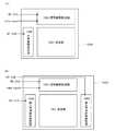
図4には、実施の形態1とは異なる実施の形態を示す。図4(A)は平面図であり、図4
(B)は図4(A)におけるQ1−Q2で切断した断面図である。FIG. 4 shows an embodiment different from the first embodiment. 4A is a plan view, and FIG.
(B) is sectional drawing cut | disconnected by Q1-Q2 in FIG. 4 (A).
図4に示す薄膜トランジスタ151は、アルミニウムを第1成分とする第1導電層(11
4a、114b)上に高融点金属材料によって形成される第2導電層(115a、115
b)を積層したソース電極層及びドレイン電極層(117a、117b)が基板100上
に形成され、ソース電極層及びドレイン電極層の高融点金属材料によって形成される第2
導電層(115a、115b)と、ソース電極層及びドレイン電極層の端部にある酸化ア
ルミニウムを第1成分とするバリア層(116a、116b)に接して、酸化物半導体層
113が形成され、酸化物半導体層113を覆うゲート絶縁膜102が形成され、ゲート
絶縁膜102を介してソース電極層及びドレイン電極層(117a、117b)の端部に
重畳するゲート電極層111が形成されている。A
4a, 114b) and second conductive layers (115a, 115) formed of a refractory metal material.
A source electrode layer and a drain electrode layer (117a, 117b) in which b) are stacked are formed on the
An
本発明の一態様では、アルミニウムを第1成分とする第1導電層(114a、114b)
と高融点の金属材料からなる第2導電層(115a、115b)を積層したソース電極層
及びドレイン電極層(117a、117b)の端部に酸化アルミニウムを第1成分とする
バリア層(116a、116b)が形成されている。そのため酸化物半導体とアルミニウ
ムを第1成分とする第1導電層は互いに直接ふれていない。In one embodiment of the present invention, the first conductive layer (114a, 114b) containing aluminum as the first component.
And barrier layers (116a, 116b) containing aluminum oxide as a first component at the ends of the source and drain electrode layers (117a, 117b) in which the second conductive layers (115a, 115b) made of a high melting point metal material are stacked. ) Is formed. Therefore, the first conductive layers containing the oxide semiconductor and aluminum as the first component are not in direct contact with each other.
図4(A)、(B)の薄膜トランジスタ151の作製方法を図5及び図6を用いて説明す
る。A method for manufacturing the
基板上に低抵抗な導電性材料であるアルミニウムを主成分とする第1導電膜上に、高融点
の金属材料からなる第2導電膜を積層して、ソース電極層及びドレイン電極層となる導電
膜を形成する。なお、基板、アルミニウムを主成分とする第1導電膜、及び高融点の金属
材料からなる第2導電膜は、実施の形態1と同様の材料を用いることができる。A second conductive film made of a metal material having a high melting point is stacked on a first conductive film mainly composed of aluminum, which is a low-resistance conductive material, on a substrate, and a conductive film that becomes a source electrode layer and a drain electrode layer. A film is formed. Note that the same material as that in
ここでは、スパッタリング法で第1導電膜と第2導電膜を積層した。次に、本実施の形態
における第1のフォトマスクを用いて形成したレジストマスクを使い、基板100上に形
成された導電膜の不要な部分をエッチングして除去して配線及び電極(ソース電極層及び
ドレイン電極層(117a、117b)を含む信号線、容量配線、及び端子)を形成する
。このとき少なくともソース電極層及びドレイン電極層(117a、117b)の端部に
テーパー形状が形成されるようにエッチングする。また、ここで形成した電極層の端部に
はアルミニウムを第1成分とする第1導電層が露出する。なお、この段階での段面図を図
5(A)に示す。Here, the first conductive film and the second conductive film were stacked by a sputtering method. Next, unnecessary portions of the conductive film formed over the
次にソース電極層及びドレイン電極層(117a、117b)の端部に露出したアルミニ
ウムを第1成分とする第1導電層を実施の形態1と同様に酸化処理し、酸化アルミニウム
を第1成分とするバリア層(116a、116b)を形成する。酸化アルミニウムを第1
成分とするバリア層の厚みは0より大で5nm以下であり、非水和酸化膜である。この段
階での段面図を図5(B)に示す。Next, the first conductive layer whose first component is aluminum exposed at the ends of the source and drain electrode layers (117a, 117b) is oxidized in the same manner as in the first embodiment, and the aluminum oxide is used as the first component. Barrier layers (116a, 116b) to be formed are formed. Aluminum oxide first
The thickness of the barrier layer as a component is greater than 0 and 5 nm or less, and is a non-hydrated oxide film. A step view at this stage is shown in FIG.
次に、酸化物半導体膜をソース電極及びドレイン電極(117a、117b)上に成膜す
る。酸化物半導体膜は、アルミニウムを第1成分とする第1導電層を酸化処理した後、大
気にさらすことなく連続して成膜するのが望ましい。連続成膜することで、水蒸気などの
大気成分や大気中に浮遊する不純物元素やゴミによる汚染がない積層界面を形成できるの
で、薄膜トランジスタ特性のばらつきを低減できる。Next, an oxide semiconductor film is formed over the source and drain electrodes (117a and 117b). The oxide semiconductor film is preferably formed continuously after the first conductive layer containing aluminum as the first component is oxidized and not exposed to the atmosphere. By performing continuous film formation, it is possible to form a laminated interface free from contamination by atmospheric components such as water vapor, impurity elements floating in the atmosphere, and dust, so that variations in thin film transistor characteristics can be reduced.
ここでは、酸化物半導体膜としてインジウム、ガリウム及び亜鉛を含む酸化物半導体を用
い、実施の形態1と同様に酸素が過剰な雰囲気で成膜し多くの酸素を酸化物半導体膜中に
含ませる。多くの酸素を酸化物半導体膜中に含ませることによってオフ電流の低減を図る
ことができるため、オン・オフ比の高い薄膜トランジスタを得ることができる。また、本
実施の形態では酸化物半導体膜の膜厚は100nmとする。Here, an oxide semiconductor containing indium, gallium, and zinc is used as the oxide semiconductor film, and is formed in an atmosphere containing excess oxygen as in
次に、本実施の形態における第2のフォトマスクを用いてレジストマスクを形成し、エッ
チングにより不要な部分を除去してインジウム、ガリウム及び亜鉛を含む酸化物半導体層
113を形成する。酸化物半導体層113のエッチングは、ウェットエッチングに限定さ
れずドライエッチングを用いてもよい。Next, a resist mask is formed using the second photomask in this embodiment, an unnecessary portion is removed by etching, and the
ここでは実施の形態1と同様にITO07N(関東化学社製)を用いたウェットエッチン
グにより、不要な部分を除去してインジウム、ガリウム及び亜鉛を含む酸化物半導体層1
13を形成する。この段階での断面図を図5(C)に示す。Here, as in
13 is formed. A cross-sectional view at this stage is illustrated in FIG.
インジウム、ガリウム、及び亜鉛を含む酸化物半導体を用いた薄膜トランジスタは、20
0℃〜600℃、代表的には300℃〜500℃の熱処理を行うことが好ましい。ここで
は炉に入れ、窒素雰囲気下で350℃、1時間の熱処理を行う。なお、熱処理は窒素雰囲
気下に限られるものではなく、大気中もしくは酸素雰囲気下であってもよい。この熱処理
によりインジウム、ガリウム及び亜鉛を含む酸化物半導体膜の原子レベルの再配列が行わ
れる。この熱処理によりキャリアの移動を阻害する歪が解放されるため、ここでの熱処理
(光アニールも含む)は重要である。なお、熱処理を行うタイミングは、酸化物半導体膜
の成膜後であれば特に限定されず、例えば画素電極形成後に行ってもよい。A thin film transistor using an oxide semiconductor containing indium, gallium, and zinc is 20
It is preferable to perform heat treatment at 0 ° C. to 600 ° C., typically 300 ° C. to 500 ° C. Here, heat treatment is performed in a furnace at 350 ° C. for 1 hour in a nitrogen atmosphere. The heat treatment is not limited to a nitrogen atmosphere, and may be in the air or an oxygen atmosphere. Through this heat treatment, rearrangement at the atomic level of the oxide semiconductor film containing indium, gallium, and zinc is performed. Since heat treatment releases strain that hinders carrier movement, heat treatment here (including optical annealing) is important. Note that the timing of performing the heat treatment is not particularly limited as long as it is after the formation of the oxide semiconductor film.
ゲート絶縁膜を形成する前に、酸化物半導体層113にプラズマ処理を行ってもよい。プ
ラズマ処理を行うことにより、エッチングによる酸化物半導体層113のダメージを回復
することができる。プラズマ処理はO2、N2O、好ましくは酸素を含むN2、He、A
r雰囲気下で行うことが好ましい。また、上記雰囲気にCl2、CF4を加えた雰囲気下
で行ってもよい。なお、プラズマ処理は、無バイアスで行うことが好ましい。Plasma treatment may be performed on the
It is preferable to perform in r atmosphere. It may also be carried out in an atmosphere obtained by addingCl 2, CF4 to the atmosphere. Note that the plasma treatment is preferably performed without bias.
次にゲート絶縁膜102を形成する。ゲート絶縁膜102としては、実施の形態1と同様
のものを用いることができ、また単層であっても、絶縁膜を2層または3層積層して形成
してもよい。ここでは、ゲート絶縁膜102としてスパッタリング法により100nmの
厚みの酸化珪素膜を成膜する。Next, the
次に、ゲート電極層111となる導電膜を成膜する。導電膜は実施の形態1と同様の材料
を用いることができる。Next, a conductive film to be the
次いで、本実施の形態における第3のフォトマスクを用いて形成したレジストマスクを使
い、導電膜の不要な部分をエッチングして除去してゲート電極層111を形成する。以上
の工程でインジウム、ガリウム及び亜鉛を含む酸化物半導体層113をチャネル形成領域
とする薄膜トランジスタ151が作製できる。この段階での段面図を図6(A)に示す。Next, using a resist mask formed using the third photomask in this embodiment, unnecessary portions of the conductive film are removed by etching, so that the
次に、薄膜トランジスタ151を覆う保護絶縁膜109を形成する。保護絶縁膜109は
スパッタリング法などを用いて得られる窒化珪素膜、酸化珪素膜、酸化窒化珪素膜などを
用いることができる。Next, a protective
次に、本実施の形態における第4のフォトマスクを用いて形成したレジストマスクにより
、保護絶縁膜109およびゲート絶縁膜102をエッチングして、ドレイン電極層107
bに達するコンタクトホール125を形成する。この段階での断面図を図6(B)に示す
。Next, the protective
A
次に、ゲート電極層111、ソース電極層及びドレイン電極層(117a、117b)に
次ぐ第三の導電層を形成する。本発明の一態様の半導体装置を表示装置に適用する場合、
第三の導電層は表示装置の画素電極や配線や端子部になる。Next, a third conductive layer is formed next to the
The third conductive layer becomes a pixel electrode, wiring, or terminal portion of the display device.
ここでは、第三の導電層として透明導電膜を成膜する。透明導電膜の材料としては、酸化
インジウム(In2O3)や酸化インジウム酸化スズ合金(In2O3―SnO2、IT
Oと略記する)などをスパッタリング法や真空蒸着法などを用いて形成する。このような
材料のエッチング処理は塩酸系の溶液により行う。しかし、特にITOのエッチングは残
渣が発生しやすいので、エッチング加工性を改善するために酸化インジウム酸化亜鉛合金
(In2O3―ZnO)を用いても良い。Here, a transparent conductive film is formed as the third conductive layer. As the material for the transparent conductive film, indium oxide (In2 O3 ), indium oxide tin oxide alloy (In2 O3 —SnO2 , IT
(Abbreviated as “O”) or the like using a sputtering method, a vacuum deposition method, or the like. Etching treatment of such a material is performed with a hydrochloric acid based solution. However, in particular, since etching of ITO is likely to generate a residue, an indium oxide-zinc oxide alloy (In2 O3 —ZnO) may be used to improve etching processability.
次に、本実施の形態における第5のフォトマスクを用いて形成したレジストマスクにより
、不要な部分をエッチングして除去して第三の導電層128を形成する。この段階での断
面図を図6(C)に示す。Next, unnecessary portions are etched away using the resist mask formed using the fifth photomask in this embodiment, so that the third
以上の方法で、図4に示す本発明の一態様の順スタガ型薄膜トランジスタを作製する。本
実施の形態で形成した薄膜トランジスタは、インジウム、ガリウム、及び亜鉛を含む酸化
物半導体層とアルミニウムを主成分とする第1導電層との間に高融点の金属材料からなる
第2導電層もしくは酸化アルミニウムを第1成分とするバリア層を形成するため、アルミ
ニウム原子の酸化物半導体層への拡散を抑制できる。特に、インジウム、ガリウム、及び
亜鉛を含む酸化物半導体層を熱処理しても、アルミニウム原子の酸化物半導体層への拡散
を抑制できる。また、インジウム、ガリウム、及び亜鉛を含む酸化物半導体層とアルミニ
ウムを第1成分とする第1導電層との間で生じる電食(電気化学的腐食ともいう)を防ぐ
ことができる。よって、信頼性のよい薄膜トランジスタを有する半導体装置を提供できる
。Through the above method, the forward staggered thin film transistor of one embodiment of the present invention illustrated in FIG. 4 is manufactured. The thin film transistor formed in this embodiment includes a second conductive layer or an oxide formed of a metal material with a high melting point between an oxide semiconductor layer containing indium, gallium, and zinc and a first conductive layer containing aluminum as a main component. Since the barrier layer containing aluminum as the first component is formed, diffusion of aluminum atoms into the oxide semiconductor layer can be suppressed. In particular, even when heat treatment is performed on an oxide semiconductor layer containing indium, gallium, and zinc, diffusion of aluminum atoms into the oxide semiconductor layer can be suppressed. In addition, electrolytic corrosion (also referred to as electrochemical corrosion) that occurs between the oxide semiconductor layer containing indium, gallium, and zinc and the first conductive layer containing aluminum as a first component can be prevented. Thus, a semiconductor device including a highly reliable thin film transistor can be provided.
(実施の形態3)
本実施の形態では、本発明の一態様の半導体装置の一例である表示装置として電子ペーパ
ーの例を示す。(Embodiment 3)
In this embodiment, an example of electronic paper is described as a display device which is an example of a semiconductor device of one embodiment of the present invention.
図7は、本発明の一態様を適用した表示装置の例としてアクティブマトリクス型の電子ペ
ーパーを示す。表示装置に用いられる薄膜トランジスタ581としては、実施の形態1又
は実施の形態2と同様に作製でき、アルミニウム原子の酸化物半導体層への拡散が抑制さ
れた信頼性のよい薄膜トランジスタである。FIG. 7 illustrates active matrix electronic paper as an example of a display device to which one embodiment of the present invention is applied. The
図7の電子ペーパーは、ツイストボール表示方式を用いた表示装置の例である。ツイスト
ボール表示方式とは、白と黒に塗り分けられた球形粒子を表示素子に用い、電極層である
第1の電極層及び第2の電極層の間に配置し、第1の電極層及び第2の電極層に電位差を
生じさせての球形粒子の向きを制御することにより、表示を行う方法である。The electronic paper in FIG. 7 is an example of a display device using a twisting ball display system. The twist ball display method uses spherical particles that are painted in white and black as a display element, and is arranged between the first electrode layer and the second electrode layer, which are electrode layers, In this method, display is performed by controlling the orientation of the spherical particles by generating a potential difference in the second electrode layer.
薄膜トランジスタ581はソース電極層又はドレイン電極層によって第1の電極層587
と、絶縁層585に形成する開口で接しており電気的に接続している。第1の電極層58
7と第2の電極層588との間には黒色領域590a及び白色領域590bを有し、周り
に液体で満たされているキャビティ594を含む球形粒子589が設けられており、球形
粒子589の周囲は樹脂等の充填材595で充填されている(図7参照。)。The
Are electrically connected to each other through an opening formed in the insulating
7 and the
また、ツイストボールの代わりに、電気泳動素子を用いることも可能である。透明な液体
と、正に帯電した白い微粒子と負に帯電した黒い微粒子とを封入した直径10μm〜20
0μm程度のマイクロカプセルを用いる。第1の電極層と第2の電極層との間に設けられ
るマイクロカプセルは、第1の電極層と第2の電極層によって、電場が与えられると、白
い微粒子と、黒い微粒子が逆の方向に移動し、白または黒を表示することができる。この
原理を応用した表示素子が電気泳動表示素子であり、一般的に電子ペーパーとよばれてい
る。電気泳動表示素子は、液晶表示素子に比べて反射率が高いため、補助ライトは不要で
あり、また消費電力が小さく、薄暗い場所でも表示部を認識することが可能である。また
、表示部に電源が供給されない場合であっても、一度表示した像を保持することが可能で
あるため、電波発信源から表示機能付き半導体装置(単に表示装置、又は表示装置を具備
する半導体装置ともいう)を遠ざけた場合であっても、表示された像を保存しておくこと
が可能となる。Further, instead of the twisting ball, an electrophoretic element can be used. A diameter of 10 μm to 20 in which transparent liquid, positively charged white fine particles, and negatively charged black fine particles are enclosed.
Use microcapsules of about 0 μm. In the microcapsule provided between the first electrode layer and the second electrode layer, when an electric field is applied by the first electrode layer and the second electrode layer, the white particles and the black particles are in opposite directions. And can display white or black. A display element using this principle is an electrophoretic display element, and is generally called electronic paper. Since the electrophoretic display element has higher reflectance than the liquid crystal display element, an auxiliary light is unnecessary, power consumption is small, and the display portion can be recognized even in a dim place. Further, even when power is not supplied to the display portion, an image once displayed can be held; therefore, a semiconductor device with a display function from a radio wave source (simply a display device or a semiconductor having a display device) Even when the device is also moved away, the displayed image can be stored.
インジウム、ガリウム、及び亜鉛を含む酸化物半導体層とアルミニウムを主成分とする第
1導電層との間に、高融点の金属材料からなる第2電極層もしくは酸化アルミニウムを第
1成分とするバリア層を設け、酸化物半導体層へのアルミニウム原子の拡散を抑制した実
施の形態1又は実施の形態2に記載の薄膜トランジスタは信頼性が高い。信頼性が高い薄
膜トランジスタを搭載した電子ペーパーは表示装置として信頼性が高い。Between the oxide semiconductor layer containing indium, gallium, and zinc and the first conductive layer containing aluminum as a main component, a second electrode layer made of a metal material having a high melting point or a barrier layer containing aluminum oxide as a first component The thin film transistor described in
(実施の形態4)
本実施の形態では、本発明の一態様の半導体装置の一例である表示装置において、同一基
板上に少なくとも駆動回路の一部と、画素部に配置する薄膜トランジスタを作製する例に
ついて図8乃至図13を用いて以下に説明する。(Embodiment 4)
In this embodiment, an example in which at least part of a driver circuit and a thin film transistor provided in a pixel portion are formed over the same substrate in a display device which is an example of a semiconductor device of one embodiment of the present invention will be described with reference to FIGS. Will be described below.
同一基板上に配置する薄膜トランジスタは、実施の形態1又は実施の形態2と同様に形成
する。また、実施の形態1又は実施の形態2と同様の方法で形成した薄膜トランジスタは
nチャネル型TFTであるため、駆動回路のうち、nチャネル型TFTで構成することが
できる駆動回路の一部を画素部の薄膜トランジスタと同一基板上に形成する。Thin film transistors placed over the same substrate are formed in the same manner as in
本発明の一態様の半導体装置の一例であるアクティブマトリクス型液晶表示装置のブロッ
ク図の一例を図8(A)に示す。図8(A)に示す表示装置は、基板5300上に表示素
子を備えた画素を複数有する画素部5301と、各画素を選択する走査線駆動回路530
2と、選択された画素へのビデオ信号の入力を制御する信号線駆動回路5303とを有す
る。FIG. 8A illustrates an example of a block diagram of an active matrix liquid crystal display device which is an example of a semiconductor device of one embodiment of the present invention. A display device illustrated in FIG. 8A includes a pixel portion 5301 including a plurality of pixels each provided with a display element over a
2 and a signal line driver circuit 5303 for controlling the input of the video signal to the selected pixel.
画素部5301は、信号線駆動回路5303から列方向に伸張して配置された複数の信号
線S1〜Sm(図示せず。)により信号線駆動回路5303と接続され、走査線駆動回路
5302から行方向に伸張して配置された複数の走査線G1〜Gn(図示せず。)により
走査線駆動回路5302と接続され、信号線S1〜Sm並びに走査線G1〜Gnに対応し
てマトリクス状に配置された複数の画素(図示せず。)を有する。そして、各画素は、信
号線Sj(信号線S1〜Smのうちいずれか一)、走査線Gi(走査線G1〜Gnのうち
いずれか一)と接続される。The pixel portion 5301 is connected to the signal line driver circuit 5303 by a plurality of signal lines S1 to Sm (not shown) arranged extending from the signal line driver circuit 5303 in the column direction. A plurality of scanning lines G1 to Gn (not shown) arranged in the direction are connected to the scanning
また、実施の形態2と同様の方法で形成できる薄膜トランジスタは、nチャネル型TFT
であり、nチャネル型TFTで構成する信号線駆動回路について図9を用いて説明する。A thin film transistor that can be formed by a method similar to that of
A signal line driver circuit including n-channel TFTs will be described with reference to FIG.
図9に示す信号線駆動回路は、ドライバIC5601、スイッチ群5602_1〜560
2_M、第1の配線5611、第2の配線5612、第3の配線5613及び配線562
1_1〜5621_Mを有する。スイッチ群5602_1〜5602_Mそれぞれは、第
1の薄膜トランジスタ5603a、第2の薄膜トランジスタ5603b及び第3の薄膜ト
ランジスタ5603cを有する。A signal line driver circuit illustrated in FIG. 9 includes a
2_M, the
1_1 to 5621_M. Each of the switch groups 5602_1 to 5602_M includes a first
ドライバIC5601は第1の配線5611、第2の配線5612、第3の配線5613
及び配線5621_1〜5621_Mに接続される。そして、スイッチ群5602_1〜
5602_Mそれぞれは、第1の配線5611、第2の配線5612、第3の配線561
3及びスイッチ群5602_1〜5602_Mそれぞれに対応した配線5621_1〜5
621_Mに接続される。そして、配線5621_1〜5621_Mそれぞれは、第1の
薄膜トランジスタ5603a、第2の薄膜トランジスタ5603b及び第3の薄膜トラン
ジスタ5603cを介して、3つの信号線に接続される。例えば、J列目の配線5621
_J(配線5621_1〜配線5621_Mのうちいずれか一)は、スイッチ群5602
_Jが有する第1の薄膜トランジスタ5603a、第2の薄膜トランジスタ5603b及
び第3の薄膜トランジスタ5603cを介して、信号線Sj−1、信号線Sj、信号線S
j+1に接続される。The
And the wirings 5621_1 to 5621_M. And switch group 5602_1-
Each of 5602_M includes a
3 and switches 5621_1 to 5602_1 to 5602_1 to 5602_M respectively.
621_M. Each of the wirings 5621_1 to 5621_M is connected to three signal lines through the first
_J (any one of the wirings 5621_1 to 5621_M) is a switch group 5602.
_J includes the signal line Sj-1, the signal line Sj, and the signal line S through the first
connected to j + 1.
なお、第1の配線5611、第2の配線5612、第3の配線5613には、それぞれ信
号が入力される。Note that a signal is input to each of the
なお、ドライバIC5601は、単結晶基板上に形成されていることが望ましい。さらに
、スイッチ群5602_1〜5602_Mは、画素部と同一基板上に形成されていること
が望ましい。したがって、ドライバIC5601とスイッチ群5602_1〜5602_
MとはFPCなどを介して接続するとよい。Note that the
It is good to connect with M through FPC or the like.
次に、図9に示した信号線駆動回路の動作について、図10のタイミングチャートを参照
して説明する。なお、図10のタイミングチャートは、i行目の走査線Giが選択されて
いる場合のタイミングチャートを示している。さらに、i行目の走査線Giの選択期間は
、第1のサブ選択期間T1、第2のサブ選択期間T2及び第3のサブ選択期間T3に分割
されている。さらに、図9の信号線駆動回路は、他の行の走査線が選択されている場合で
も図10と同様の動作をする。Next, operation of the signal line driver circuit illustrated in FIG. 9 is described with reference to a timing chart of FIG. Note that the timing chart of FIG. 10 shows the timing chart when the i-th scanning line Gi is selected. Further, the selection period of the i-th scanning line Gi is divided into a first sub-selection period T1, a second sub-selection period T2, and a third sub-selection period T3. Further, the signal line driver circuit in FIG. 9 operates in the same manner as in FIG. 10 even when a scan line in another row is selected.
なお、図10のタイミングチャートは、J列目の配線5621_Jが第1の薄膜トランジ
スタ5603a、第2の薄膜トランジスタ5603b及び第3の薄膜トランジスタ560
3cを介して、信号線Sj−1、信号線Sj、信号線Sj+1に接続される場合について
示している。Note that in the timing chart of FIG. 10, the wiring 5621_J in the J-th column includes the first
A case where the signal line Sj−1, the signal line Sj, and the signal line Sj + 1 are connected via 3c is illustrated.
なお、図10のタイミングチャートは、i行目の走査線Giが選択されるタイミング、第
1の薄膜トランジスタ5603aのオン・オフのタイミング5703a、第2の薄膜トラ
ンジスタ5603bのオン・オフのタイミング5703b、第3の薄膜トランジスタ56
03cのオン・オフのタイミング5703c及びJ列目の配線5621_Jに入力される
信号5721_Jを示している。Note that in the timing chart of FIG. 10, the timing at which the i-th scanning line Gi is selected, the on / off timing 5703a of the first
In addition, an ON / OFF timing 5703c of 03c and a signal 5721_J input to the wiring 5621_J in the J-th column are illustrated.
なお、配線5621_1〜配線5621_Mには第1のサブ選択期間T1、第2のサブ選
択期間T2及び第3のサブ選択期間T3において、それぞれ別のビデオ信号が入力される
。例えば、第1のサブ選択期間T1において配線5621_Jに入力されるビデオ信号は
信号線Sj−1に入力され、第2のサブ選択期間T2において配線5621_Jに入力さ
れるビデオ信号は信号線Sjに入力され、第3のサブ選択期間T3において配線5621
_Jに入力されるビデオ信号は信号線Sj+1に入力される。さらに、第1のサブ選択期
間T1、第2のサブ選択期間T2及び第3のサブ選択期間T3において、配線5621_
Jに入力されるビデオ信号をそれぞれData_j−1、Data_j、Data_j+
1とする。Note that different video signals are input to the wirings 5621_1 to 5621_M in the first sub-selection period T1, the second sub-selection period T2, and the third sub-selection period T3. For example, a video signal input to the wiring 5621_J in the first sub-selection period T1 is input to the signal line Sj-1, and a video signal input to the wiring 5621_J in the second sub-selection period T2 is input to the signal line Sj. In the third sub-selection period T3, the wiring 5621
The video signal input to _J is input to the signal
The video signals input to J are represented by Data_j-1, Data_j, Data_j +, respectively.
Set to 1.
図10に示すように、第1のサブ選択期間T1において第1の薄膜トランジスタ5603
aがオンし、第2の薄膜トランジスタ5603b及び第3の薄膜トランジスタ5603c
がオフする。このとき、配線5621_Jに入力されるData_j−1が、第1の薄膜
トランジスタ5603aを介して信号線Sj−1に入力される。第2のサブ選択期間T2
では、第2の薄膜トランジスタ5603bがオンし、第1の薄膜トランジスタ5603a
及び第3の薄膜トランジスタ5603cがオフする。このとき、配線5621_Jに入力
されるData_jが、第2の薄膜トランジスタ5603bを介して信号線Sjに入力さ
れる。第3のサブ選択期間T3では、第3の薄膜トランジスタ5603cがオンし、第1
の薄膜トランジスタ5603a及び第2の薄膜トランジスタ5603bがオフする。この
とき、配線5621_Jに入力されるData_j+1が、第3の薄膜トランジスタ56
03cを介して信号線Sj+1に入力される。As shown in FIG. 10, the first thin film transistor 5603 in the first sub-selection period T1.
a turns on, the second
Turns off. At this time, Data_j−1 input to the wiring 5621_J is input to the signal line Sj−1 through the first
Then, the second
Then, the third
The
The signal is input to the signal line Sj + 1 via 03c.
以上のことから、図9の信号線駆動回路は、1ゲート選択期間を3つに分割することで、
1ゲート選択期間中に1つの配線5621から3つの信号線にビデオ信号を入力すること
ができる。したがって、図9の信号線駆動回路は、ドライバIC5601が形成される基
板と、画素部が形成されている基板との接続数を信号線の数に比べて約1/3にすること
ができる。接続数が約1/3になることによって、図9の信号線駆動回路は、信頼性、歩
留まりなどを向上できる。From the above, the signal line driver circuit of FIG. 9 divides one gate selection period into three,
Video signals can be input from one wiring 5621 to three signal lines during one gate selection period. Therefore, the signal line driver circuit in FIG. 9 can reduce the number of connections between the substrate on which the
なお、図9のように、1ゲート選択期間を複数のサブ選択期間に分割し、複数のサブ選択
期間それぞれにおいて、ある1つの配線から複数の信号線それぞれにビデオ信号を入力す
ることができれば、薄膜トランジスタの配置や数、駆動方法などは限定されない。As shown in FIG. 9, if one gate selection period is divided into a plurality of sub-selection periods and a video signal can be input from a certain wiring to each of a plurality of signal lines in each of the plurality of sub-selection periods, The arrangement and number of thin film transistors and the driving method are not limited.
例えば、3つ以上のサブ選択期間それぞれにおいて1つの配線から3つ以上の信号線それ
ぞれにビデオ信号を入力する場合は、薄膜トランジスタ及び薄膜トランジスタを制御する
ための配線を追加すればよい。ただし、1ゲート選択期間を4つ以上のサブ選択期間に分
割すると、1つのサブ選択期間が短くなる。したがって、1ゲート選択期間は、2つ又は
3つのサブ選択期間に分割されることが望ましい。For example, when video signals are input from one wiring to each of three or more signal lines in each of three or more sub-selection periods, a thin film transistor and a wiring for controlling the thin film transistor may be added. However, if one gate selection period is divided into four or more sub selection periods, one sub selection period is shortened. Therefore, it is desirable that one gate selection period is divided into two or three sub selection periods.
別の例として、図11のタイミングチャートに示すように、1つの選択期間をプリチャー
ジ期間Tp、第1のサブ選択期間T1、第2のサブ選択期間T2、第3の選択期間T3に
分割してもよい。さらに、図11のタイミングチャートは、i行目の走査線Giが選択さ
れるタイミング、第1の薄膜トランジスタ5603aのオン・オフのタイミング5803
a、第2の薄膜トランジスタ5603bのオン・オフのタイミング5803b、第3の薄
膜トランジスタ5603cのオン・オフのタイミング5803c及びJ列目の配線562
1_Jに入力される信号5821_Jを示している。図11に示すように、プリチャージ
期間Tpにおいて第1の薄膜トランジスタ5603a、第2の薄膜トランジスタ5603
b及び第3の薄膜トランジスタ5603cがオンする。このとき、配線5621_Jに入
力されるプリチャージ電圧Vpが第1の薄膜トランジスタ5603a、第2の薄膜トラン
ジスタ5603b及び第3の薄膜トランジスタ5603cを介してそれぞれ信号線Sj−
1、信号線Sj、信号線Sj+1に入力される。第1のサブ選択期間T1において第1の
薄膜トランジスタ5603aがオンし、第2の薄膜トランジスタ5603b及び第3の薄
膜トランジスタ5603cがオフする。このとき、配線5621_Jに入力されるDat
a_j−1が、第1の薄膜トランジスタ5603aを介して信号線Sj−1に入力される
。第2のサブ選択期間T2では、第2の薄膜トランジスタ5603bがオンし、第1の薄
膜トランジスタ5603a及び第3の薄膜トランジスタ5603cがオフする。このとき
、配線5621_Jに入力されるData_jが、第2の薄膜トランジスタ5603bを
介して信号線Sjに入力される。第3のサブ選択期間T3では、第3の薄膜トランジスタ
5603cがオンし、第1の薄膜トランジスタ5603a及び第2の薄膜トランジスタ5
603bがオフする。このとき、配線5621_Jに入力されるData_j+1が、第
3の薄膜トランジスタ5603cを介して信号線Sj+1に入力される。As another example, as shown in the timing chart of FIG. 11, one selection period is divided into a precharge period Tp, a first sub selection period T1, a second sub selection period T2, and a third selection period T3. May be. Further, in the timing chart of FIG. 11, the timing at which the i-th scanning line Gi is selected, the on / off timing 5803 of the first
a, ON /
The signal 5821_J input to 1_J is shown. As shown in FIG. 11, the first
b and the third
1 is input to the signal line Sj and the signal
a_j−1 is input to the signal line Sj−1 through the first
603b is turned off. At this time, Data_j + 1 input to the wiring 5621_J is input to the signal line Sj + 1 through the third
以上のことから、図11のタイミングチャートを適用した図9の信号線駆動回路は、サブ
選択期間の前にプリチャージ期間を設けることによって、信号線をプリチャージできるた
め、画素へのビデオ信号の書き込みを高速に行うことができる。なお、図11において、
図10と同様なものに関しては共通の符号を用いて示し、同一部分又は同様な機能を有す
る部分の詳細な説明は省略する。From the above, the signal line driver circuit in FIG. 9 to which the timing chart in FIG. 11 is applied can precharge the signal line by providing the precharge period before the sub selection period. Writing can be performed at high speed. In FIG. 11,
Components similar to those in FIG. 10 are denoted by common reference numerals, and detailed description of the same portions or portions having similar functions is omitted.
また、走査線駆動回路の構成について説明する。走査線駆動回路は、シフトレジスタ、バ
ッファを有している。また場合によってはレベルシフタを有していても良い。走査線駆動
回路において、シフトレジスタにクロック信号(CLK)及びスタートパルス信号(SP
)が入力されることによって、選択信号が生成される。生成された選択信号はバッファに
おいて緩衝増幅され、対応する走査線に供給される。走査線には、1ライン分の画素のト
ランジスタのゲート電極が接続されている。そして、1ライン分の画素のトランジスタを
一斉にONにしなくてはならないので、バッファは大きな電流を流すことが可能なものが
用いられる。A structure of the scan line driver circuit will be described. The scan line driver circuit includes a shift register and a buffer. In some cases, a level shifter may be provided. In the scan line driver circuit, a clock signal (CLK) and a start pulse signal (SP
) Is input, a selection signal is generated. The generated selection signal is buffered and amplified in the buffer and supplied to the corresponding scanning line. A gate electrode of a transistor of a pixel for one line is connected to the scanning line. Since the transistors of pixels for one line must be turned on all at once, a buffer that can flow a large current is used.
走査線駆動回路の一部に用いるシフトレジスタの一形態について図12及び図13を用い
て説明する。One mode of a shift register used for part of the scan line driver circuit is described with reference to FIGS.
図12にシフトレジスタの回路構成を示す。図12に示すシフトレジスタは、フリップフ
ロップ5701_1〜5701_nという複数のフリップフロップで構成される。また、
第1のクロック信号、第2のクロック信号、スタートパルス信号、リセット信号が入力さ
れて動作する。FIG. 12 shows a circuit configuration of the shift register. The shift register illustrated in FIG. 12 includes a plurality of flip-flops, flip-flops 5701_1 to 5701_n. Also,
The first clock signal, the second clock signal, the start pulse signal, and the reset signal are input to operate.
図12のシフトレジスタの接続関係について説明する。図12のシフトレジスタは、i段
目のフリップフロップ5701_i(フリップフロップ5701_1〜5701_nのう
ちいずれか一)は、図13に示した第1の配線5501が第7の配線5717_i−1に
接続され、図13に示した第2の配線5502が第7の配線5717_i+1に接続され
、図13に示した第3の配線5503が第7の配線5717_iに接続され、図13に示
した第6の配線5506が第5の配線5715に接続される。Connection relations of the shift register in FIG. 12 are described. In the shift register in FIG. 12, the i-th flip-flop 5701_i (any one of the flip-flops 5701_1 to 5701_n) has the
また、図13に示した第4の配線5504が奇数段目のフリップフロップでは第2の配線
5712に接続され、偶数段目のフリップフロップでは第3の配線5713に接続され、
図13に示した第5の配線5505が第4の配線5714に接続される。The
The
ただし、1段目のフリップフロップ5701_1の図13に示す第1の配線5501は第
1の配線5711に接続され、n段目のフリップフロップ5701_nの図13に示す第
2の配線5502は第6の配線5716に接続される。Note that the
なお、第1の配線5711、第2の配線5712、第3の配線5713、第6の配線57
16を、それぞれ第1の信号線、第2の信号線、第3の信号線、第4の信号線と呼んでも
よい。さらに、第4の配線5714、第5の配線5715を、それぞれ第1の電源線、第
2の電源線と呼んでもよい。Note that the
16 may be referred to as a first signal line, a second signal line, a third signal line, and a fourth signal line, respectively. Further, the
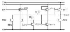
次に、図12に示すフリップフロップの詳細について、図13に示す。図13に示すフリ
ップフロップは、第1の薄膜トランジスタ5571、第2の薄膜トランジスタ5572、
第3の薄膜トランジスタ5573、第4の薄膜トランジスタ5574、第5の薄膜トラン
ジスタ5575、第6の薄膜トランジスタ5576、第7の薄膜トランジスタ5577及
び第8の薄膜トランジスタ5578を有する。なお、第1の薄膜トランジスタ5571、
第2の薄膜トランジスタ5572、第3の薄膜トランジスタ5573、第4の薄膜トラン
ジスタ5574、第5の薄膜トランジスタ5575、第6の薄膜トランジスタ5576、
第7の薄膜トランジスタ5577及び第8の薄膜トランジスタ5578は、nチャネル型
トランジスタであり、ゲート・ソース間電圧(Vgs)がしきい値電圧(Vth)を上回
ったとき導通状態になるものとする。Next, FIG. 13 shows details of the flip-flop shown in FIG. The flip-flop illustrated in FIG. 13 includes a first
A third
The second
The seventh
次に、図13に示すフリップフロップの接続構成について、以下に示す。Next, a connection structure of the flip-flop illustrated in FIG. 13 is described below.
第1の薄膜トランジスタ5571の第1の電極(ソース電極またはドレイン電極の一方)
が第4の配線5504に接続され、第1の薄膜トランジスタ5571の第2の電極(ソー
ス電極またはドレイン電極の他方)が第3の配線5503に接続される。First electrode of the first thin film transistor 5571 (one of a source electrode and a drain electrode)
Is connected to the
第2の薄膜トランジスタ5572の第1の電極が第6の配線5506に接続され、第2の
薄膜トランジスタ5572第2の電極が第3の配線5503に接続される。A first electrode of the second
第3の薄膜トランジスタ5573の第1の電極が第5の配線5505に接続され、第3の
薄膜トランジスタ5573の第2の電極が第2の薄膜トランジスタ5572のゲート電極
に接続され、第3の薄膜トランジスタ5573のゲート電極が第5の配線5505に接続
される。The first electrode of the third
第4の薄膜トランジスタ5574の第1の電極が第6の配線5506に接続され、第4の
薄膜トランジスタ5574の第2の電極が第2の薄膜トランジスタ5572のゲート電極
に接続され、第4の薄膜トランジスタ5574のゲート電極が第1の薄膜トランジスタ5
571のゲート電極に接続される。The first electrode of the fourth
571 is connected to the gate electrode.
第5の薄膜トランジスタ5575の第1の電極が第5の配線5505に接続され、第5の
薄膜トランジスタ5575の第2の電極が第1の薄膜トランジスタ5571のゲート電極
に接続され、第5の薄膜トランジスタ5575のゲート電極が第1の配線5501に接続
される。The first electrode of the fifth
第6の薄膜トランジスタ5576の第1の電極が第6の配線5506に接続され、第6の
薄膜トランジスタ5576の第2の電極が第1の薄膜トランジスタ5571のゲート電極
に接続され、第6の薄膜トランジスタ5576のゲート電極が第2の薄膜トランジスタ5
572のゲート電極に接続される。The first electrode of the sixth
572 is connected to the gate electrode.
第7の薄膜トランジスタ5577の第1の電極が第6の配線5506に接続され、第7の
薄膜トランジスタ5577の第2の電極が第1の薄膜トランジスタ5571のゲート電極
に接続され、第7の薄膜トランジスタ5577のゲート電極が第2の配線5502に接続
される。第8の薄膜トランジスタ5578の第1の電極が第6の配線5506に接続され
、第8の薄膜トランジスタ5578の第2の電極が第2の薄膜トランジスタ5572のゲ
ート電極に接続され、第8の薄膜トランジスタ5578のゲート電極が第1の配線550
1に接続される。The first electrode of the seventh
1 is connected.
なお、第1の薄膜トランジスタ5571のゲート電極、第4の薄膜トランジスタ5574
のゲート電極、第5の薄膜トランジスタ5575の第2の電極、第6の薄膜トランジスタ
5576の第2の電極及び第7の薄膜トランジスタ5577の第2の電極の接続箇所をノ
ード5543とする。さらに、第2の薄膜トランジスタ5572のゲート電極、第3の薄
膜トランジスタ5573の第2の電極、第4の薄膜トランジスタ5574の第2の電極、
第6の薄膜トランジスタ5576のゲート電極及び第8の薄膜トランジスタ5578の第
2の電極の接続箇所をノード5544とする。Note that the gate electrode of the first
A connection position of the second electrode of the fifth
A connection position between the gate electrode of the sixth
なお、第1の配線5501、第2の配線5502、第3の配線5503及び第4の配線5
504を、それぞれ第1の信号線、第2の信号、第3の信号線、第4の信号線と呼んでも
よい。さらに、第5の配線5505を第1の電源線、第6の配線5506を第2の電源線
と呼んでもよい。Note that the
504 may be referred to as a first signal line, a second signal, a third signal line, and a fourth signal line, respectively. Further, the
また、信号線駆動回路及び走査線駆動回路を、実施の形態2と同様の方法で形成できるn
チャネル型TFTのみをつかって作製することも可能である。実施の形態2と同様の方法
で形成できるnチャネル型TFTはトランジスタの移動度が大きいため、駆動回路の駆動
周波数を高くすることが可能となる。例えば、実施の形態2と同様の方法で形成できるn
チャネル型TFTを用いた走査線駆動回路は、高速に動作させることが出来るため、フレ
ーム周波数を高くすること、または、黒画面挿入を実現することなども実現することが出
来る。In addition, the signal line driver circuit and the scan line driver circuit can be formed by a method similar to that in
It is also possible to manufacture using only channel TFTs. An n-channel TFT that can be formed by a method similar to that in
Since a scanning line driver circuit using a channel type TFT can be operated at high speed, a frame frequency can be increased or a black screen can be inserted.
さらに、走査線駆動回路のトランジスタのチャネル幅を大きくすることや、複数の走査線
駆動回路を配置することなどによって、さらに高いフレーム周波数を実現することが出来
る。複数の走査線駆動回路を配置する場合は、偶数行の走査線を駆動する為の走査線駆動
回路を片側に配置し、奇数行の走査線を駆動するための走査線駆動回路をその反対側に配
置することにより、フレーム周波数を高くすることを実現することができる。また、複数
の走査線駆動回路により、同じ走査線に信号を出力すると、表示装置の大型化に有利であ
る。Further, a higher frame frequency can be realized by increasing the channel width of the transistor of the scan line driver circuit or disposing a plurality of scan line driver circuits. When a plurality of scanning line driving circuits are arranged, a scanning line driving circuit for driving even-numbered scanning lines is arranged on one side, and a scanning line driving circuit for driving odd-numbered scanning lines is arranged on the opposite side. By arranging them in this manner, it is possible to increase the frame frequency. In addition, when a plurality of scanning line driving circuits outputs signals to the same scanning line, it is advantageous for increasing the size of the display device.
また、本発明の一態様を適用した半導体装置の一例であるアクティブマトリクス型発光表
示装置を作製する場合、少なくとも一つの画素に複数の薄膜トランジスタを配置するため
、走査線駆動回路を複数配置することが好ましい。アクティブマトリクス型発光表示装置
のブロック図の一例を図8(B)に示す。In the case of manufacturing an active matrix light-emitting display device which is an example of a semiconductor device to which one embodiment of the present invention is applied, a plurality of thin film transistors are provided in at least one pixel, and thus a plurality of scan line driver circuits may be provided. preferable. An example of a block diagram of an active matrix light-emitting display device is illustrated in FIG.
図8(B)に示す発光表示装置は、基板5400上に表示素子を備えた画素を複数有する
画素部5401と、各画素を選択する第1の走査線駆動回路5402及び第2の走査線駆
動回路5404と、選択された画素へのビデオ信号の入力を制御する信号線駆動回路54
03とを有する。A light-emitting display device illustrated in FIG. 8B includes a pixel portion 5401 having a plurality of pixels each provided with a display element over a
03.
図8(B)に示す発光表示装置の画素に入力されるビデオ信号をデジタル形式とする場合
、画素はトランジスタのオンとオフの切り替えによって、発光もしくは非発光の状態とな
る。よって、面積階調法または時間階調法を用いて階調の表示を行うことができる。面積
階調法は、1画素を複数の副画素に分割し、各副画素を独立にビデオ信号に基づいて駆動
させることによって、階調表示を行う駆動法である。また時間階調法は、画素が発光する
期間を制御することによって、階調表示を行う駆動法である。In the case where a video signal input to the pixel of the light-emitting display device illustrated in FIG. 8B is in a digital format, the pixel is turned on or off by switching on and off of the transistor. Therefore, gradation display can be performed using the area gradation method or the time gradation method. The area gradation method is a driving method in which gradation display is performed by dividing one pixel into a plurality of subpixels and independently driving each subpixel based on a video signal. The time gray scale method is a driving method for performing gray scale display by controlling a period during which a pixel emits light.
発光素子は、液晶素子などに比べて応答速度が高いので、液晶素子よりも時間階調法に適
している。具体的に時間階調法で表示を行なう場合、1フレーム期間を複数のサブフレー
ム期間に分割する。そしてビデオ信号に従い、各サブフレーム期間において画素の発光素
子を発光または非発光の状態にする。複数のサブフレーム期間に分割することによって、
1フレーム期間中に画素が実際に発光する期間のトータルの長さを、ビデオ信号により制
御することができ、階調を表示することができる。Since a light emitting element has a higher response speed than a liquid crystal element or the like, it is more suitable for a time gray scale method than a liquid crystal element. Specifically, when displaying by the time gray scale method, one frame period is divided into a plurality of subframe periods. Then, in accordance with the video signal, the light emitting element of the pixel is turned on or off in each subframe period. By dividing into multiple subframe periods,
The total length of a period during which a pixel actually emits light during one frame period can be controlled by a video signal, so that gradation can be displayed.
なお、図8(B)に示す発光表示装置では、一つの画素に2つのスイッチング用TFTを
配置する場合、一方のスイッチング用TFTのゲート配線である第1の走査線に入力され
る信号を第1走査線駆動回路5402で生成し、他方のスイッチング用TFTのゲート配
線である第2の走査線に入力される信号を第2の走査線駆動回路5404で生成している
例を示しているが、第1の走査線に入力される信号と、第2の走査線に入力される信号と
を、共に1つの走査線駆動回路で生成するようにしても良い。また、例えば、1つの画素
が有するスイッチング用TFTの数によって、スイッチング素子の動作を制御するのに用
いられる走査線が、各画素に複数設けられることもあり得る。この場合、複数の走査線に
入力される信号を、全て1つの走査線駆動回路で生成しても良いし、複数の各走査線駆動
回路で生成しても良い。Note that in the light-emitting display device illustrated in FIG. 8B, when two switching TFTs are provided in one pixel, a signal input to the first scanning line which is a gate wiring of one switching TFT is input to the first TFT. An example is shown in which a signal generated by one scanning
また、発光表示装置においても、駆動回路のうち、nチャネル型TFTで構成することが
できる駆動回路の一部を画素部の薄膜トランジスタと同一基板上に形成することができる
。また、信号線駆動回路及び走査線駆動回路を実施の形態2と同様の方法で形成できるn
チャネル型TFTのみで作製することも可能である。In the light-emitting display device, part of a driver circuit that can include n-channel TFTs among driver circuits can be formed over the same substrate as the thin film transistor in the pixel portion. Further, the signal line driver circuit and the scan line driver circuit can be formed by the same method as in the second embodiment.
It is also possible to manufacture only with a channel type TFT.
また、上述した駆動回路は、液晶表示装置や発光表示装置に限らず、スイッチング素子と
電気的に接続する素子を利用して電子インクを駆動させる電子ペーパーに用いてもよい。
電子ペーパーは、電気泳動表示装置(電気泳動ディスプレイ)も呼ばれており、紙と同じ
読みやすさ、他の表示装置に比べ低消費電力、薄くて軽い形状とすることが可能という利
点を有している。The driving circuit described above is not limited to a liquid crystal display device or a light-emitting display device, and may be used for electronic paper that drives electronic ink using an element that is electrically connected to a switching element.
Electronic paper is also called an electrophoretic display device (electrophoretic display), and has the same readability as paper, low power consumption compared to other display devices, and the advantage that it can be made thin and light. ing.
電気泳動ディスプレイは、様々な形態が考えられ得るが、プラスの電荷を有する第1の粒
子と、マイナスの電荷を有する第2の粒子とを含むマイクロカプセルが溶媒または溶質に
複数分散されたものであり、マイクロカプセルに電界を印加することによって、マイクロ
カプセル中の粒子を互いに反対方向に移動させて一方側に集合した粒子の色のみを表示す
るものである。なお、第1の粒子または第2の粒子は染料を含み、電界がない場合におい
て移動しないものである。また、第1の粒子の色と第2の粒子の色は異なるもの(無色を
含む)とする。The electrophoretic display can be considered in various forms, and a plurality of microcapsules including first particles having a positive charge and second particles having a negative charge are dispersed in a solvent or a solute. In other words, by applying an electric field to the microcapsules, the particles in the microcapsules are moved in opposite directions to display only the color of the particles assembled on one side. Note that the first particle or the second particle contains a dye and does not move in the absence of an electric field. In addition, the color of the first particles and the color of the second particles are different (including colorless).
このように、電気泳動ディスプレイは、誘電定数の高い物質が高い電界領域に移動する、
いわゆる誘電泳動的効果を利用したディスプレイである。電気泳動ディスプレイは、液晶
表示装置には必要な偏光板、対向基板も電気泳動表示装置には必要なく、厚さや重さが半
減する。In this way, the electrophoretic display moves a substance having a high dielectric constant to a high electric field region.
This is a display using the so-called dielectrophoretic effect. In the electrophoretic display, the polarizing plate and the counter substrate necessary for the liquid crystal display device are not necessary for the electrophoretic display device, and the thickness and weight are reduced by half.
上記マイクロカプセルを溶媒中に分散させたものが電子インクと呼ばれるものであり、こ
の電子インクはガラス、プラスチック、布、紙などの表面に印刷することができる。また
、カラーフィルタや色素を有する粒子を用いることによってカラー表示も可能である。A solution in which the above microcapsules are dispersed in a solvent is referred to as electronic ink. This electronic ink can be printed on a surface of glass, plastic, cloth, paper, or the like. Color display is also possible by using particles having color filters or pigments.
また、アクティブマトリクス基板上に適宜、二つの電極の間に挟まれるように上記マイク
ロカプセルを複数配置すればアクティブマトリクス型の表示装置が完成し、マイクロカプ
セルに電界を印加すれば表示を行うことができる。例えば、実施の形態2と同様の方法で
形成できる薄膜トランジスタによって得られるアクティブマトリクス基板を用いることが
できる。In addition, an active matrix display device can be completed by arranging a plurality of the above microcapsules so as to be appropriately sandwiched between two electrodes on an active matrix substrate, and display can be performed by applying an electric field to the microcapsules. it can. For example, an active matrix substrate obtained by a thin film transistor that can be formed by a method similar to that in
なお、マイクロカプセル中の第1の粒子および第2の粒子は、導電体材料、絶縁体材料、
半導体材料、磁性材料、液晶材料、強誘電性材料、エレクトロルミネセント材料、エレク
トロクロミック材料、磁気泳動材料から選ばれた一種の材料、またはこれらの複合材料を
用いればよい。Note that the first particle and the second particle in the microcapsule are a conductor material, an insulator material,
A material selected from semiconductor materials, magnetic materials, liquid crystal materials, ferroelectric materials, electroluminescent materials, electrochromic materials, and magnetophoretic materials, or a composite material thereof may be used.
インジウム、ガリウム、及び亜鉛を含む酸化物半導体層とアルミニウムを主成分とする第
1導電層との間に、高融点の金属材料からなる第2導電層もしくは酸化アルミニウムを第
1成分とするバリア層を設け、酸化物半導体層へのアルミニウム原子の拡散を抑制した実
施の形態1又は実施の形態2に記載の薄膜トランジスタは信頼性が高い。以上の工程によ
り、アルミニウム原子の酸化物半導体層への拡散を抑制した信頼性のよい薄膜トランジス
タを搭載した信頼性の高い表示装置を作製することができる。なお、本実施の形態は、他
の実施の形態に記載した構成と適宜組み合わせて実施することが可能である。Between the oxide semiconductor layer containing indium, gallium, and zinc and the first conductive layer containing aluminum as a main component, a second conductive layer made of a metal material having a high melting point or a barrier layer containing aluminum oxide as a first component The thin film transistor described in
(実施の形態5)
本発明の一態様の薄膜トランジスタを作製し、該薄膜トランジスタを画素部、さらには駆
動回路に用いて表示機能を有する半導体装置(表示装置ともいう)を作製することができ
る。また、本発明の一態様の薄膜トランジスタを駆動回路の一部または全体を、画素部と
同じ基板上に一体形成し、システムオンパネルを形成することができる。(Embodiment 5)
A thin film transistor of one embodiment of the present invention is manufactured, and a semiconductor device having a display function (also referred to as a display device) can be manufactured using the thin film transistor in a pixel portion and further in a driver circuit. In addition, part or the whole of the driver circuit of the thin film transistor of one embodiment of the present invention can be formed over the same substrate as the pixel portion to form a system-on-panel.
表示装置は表示素子を含む。表示素子としては液晶素子(液晶表示素子ともいう)、発光
素子(発光表示素子ともいう)を用いることができる。発光素子は、電流または電圧によ
って輝度が制御される素子をその範疇に含んでおり、具体的には無機EL(Electr
o Luminescence)素子、有機EL素子等が含まれる。また、電子インクな
ど、電気的作用によりコントラストが変化する表示媒体も適用することができる。The display device includes a display element. As the display element, a liquid crystal element (also referred to as a liquid crystal display element) or a light-emitting element (also referred to as a light-emitting display element) can be used. A light-emitting element includes an element whose luminance is controlled by current or voltage, specifically, an inorganic EL (Electr EL).
o Luminescence) element, organic EL element and the like. In addition, a display medium whose contrast is changed by an electric effect, such as electronic ink, can be used.
また、表示装置は、表示素子が封止された状態にあるパネルと、該パネルにコントローラ
を含むIC等を実装した状態にあるモジュールとを含む。さらに本発明の一態様は、該表
示装置を作製する過程における、表示素子が完成する前の一形態に相当する素子基板に関
し、該素子基板は、電流を表示素子に供給するための手段を複数の各画素に備える。素子
基板は、具体的には、表示素子の画素電極のみが形成された状態であっても良いし、画素
電極となる導電膜を成膜した後であって、エッチングして画素電極を形成する前の状態で
あっても良いし、あらゆる形態があてはまる。The display device includes a panel in which the display element is sealed, and a module in which an IC including a controller is mounted on the panel. Further, one embodiment of the present invention relates to an element substrate corresponding to one embodiment before the display element is completed in the process of manufacturing the display device, and the element substrate includes a plurality of means for supplying current to the display element. For each pixel. Specifically, the element substrate may be in a state where only the pixel electrode of the display element is formed, or after the conductive film to be the pixel electrode is formed, the pixel electrode is formed by etching. The previous state may be used, and all forms are applicable.
なお、本明細書中における表示装置とは、画像表示デバイス、表示デバイス、もしくは光
源(照明装置含む)を指す。また、コネクター、例えばFPC(Flexible pr
inted circuit)もしくはTAB(Tape Automated Bon
ding)テープもしくはTCP(Tape Carrier Package)が取り
付けられたモジュール、TABテープやTCPの先にプリント配線板が設けられたモジュ
ール、または表示素子にCOG(Chip On Glass)方式によりIC(集積回
路)が直接実装されたモジュールも全て表示装置に含むものとする。Note that a display device in this specification means an image display device, a display device, or a light source (including a lighting device). Also, a connector such as an FPC (Flexible pr
integrated circuit) or TAB (Tape Automated Bon)
ding) tape or TCP (Tape Carrier Package) attached module, TAB tape or TCP is provided with a printed wiring board, or a display element is an IC (integrated circuit) by COG (Chip On Glass) method. All directly mounted modules are included in the display device.
本実施の形態では、本発明の一態様の半導体装置の一形態に相当する液晶表示パネルの外
観及び断面について、図14を用いて説明する。図14(A)は、第1の基板4001上
に形成された、インジウム、ガリウム、及び亜鉛を含む酸化物半導体層とアルミニウムを
主成分とする第1導電層との間に、高融点の金属材料からなる第2導電層もしくは酸化ア
ルミニウムを第1成分とするバリア層を設け、酸化物半導体層へのアルミニウム原子の拡
散を抑制した電気特性の高い薄膜トランジスタ4010、4011、及び液晶素子401
3を、第2の基板4006との間にシール材4005によって封止した、パネルの上面図
であり、図14(B)は、図14(A1)(A2)のM−Nにおける断面図に相当する。In this embodiment, the appearance and a cross section of a liquid crystal display panel, which is an embodiment of a semiconductor device of one embodiment of the present invention, will be described with reference to FIGS. FIG. 14A illustrates a metal having a high melting point between an oxide semiconductor layer containing indium, gallium, and zinc formed over the
3 is a top view of the panel sealed with the
第1の基板4001上に設けられた画素部4002と、走査線駆動回路4004とを囲む
ようにして、シール材4005が設けられている。また画素部4002と、走査線駆動回
路4004の上に第2の基板4006が設けられている。よって画素部4002と、走査
線駆動回路4004とは、第1の基板4001とシール材4005と第2の基板4006
とによって、液晶層4008と共に封止されている。また第1の基板4001上のシール
材4005によって囲まれている領域とは異なる領域に、別途用意された基板上に単結晶
半導体膜又は多結晶半導体膜で形成された信号線駆動回路4003が実装されている。A
Are sealed together with the
なお、別途形成した駆動回路の接続方法は、特に限定されるものではなく、COG方法、
ワイヤボンディング方法、或いはTAB方法などを用いることができる。図14(A1)
は、COG方法により信号線駆動回路4003を実装する例であり、図14(A2)は、
TAB方法により信号線駆動回路4003を実装する例である。Note that a connection method of a separately formed drive circuit is not particularly limited, and a COG method,
A wire bonding method, a TAB method, or the like can be used. FIG. 14 (A1)
Is an example in which the signal
In this example, the signal
また第1の基板4001上に設けられた画素部4002と、走査線駆動回路4004は、
薄膜トランジスタを複数有しており、図14(B)では、画素部4002に含まれる薄膜
トランジスタ4010と、走査線駆動回路4004に含まれる薄膜トランジスタ4011
とを例示している。薄膜トランジスタ4010、4011上には絶縁層4020、402
1が設けられている。In addition, the
In FIG. 14B, a
And are illustrated. Insulating
1 is provided.
薄膜トランジスタ4010、4011は、アルミニウム原子の酸化物半導体層への拡散を
抑制した信頼性のよい薄膜トランジスタに相当し、実施の形態1又は実施の形態2に示す
薄膜トランジスタを適用することができる。本実施の形態において、薄膜トランジスタ4
010、4011はnチャネル型薄膜トランジスタである。The
また、液晶素子4013が有する画素電極層4030は、薄膜トランジスタ4010と電
気的に接続されている。そして液晶素子4013の対向電極層4031は第2の基板40
06上に形成されている。画素電極層4030と対向電極層4031と液晶層4008と
が重なっている部分が、液晶素子4013に相当する。なお、画素電極層4030、対向
電極層4031はそれぞれ配向膜として機能する絶縁層4032、4033が設けられ、
絶縁層4032、4033を介して液晶層4008を挟持している。In addition, the
06 is formed. A portion where the
A
なお、第1の基板4001、第2の基板4006としては、ガラス、金属(代表的にはス
テンレス)、セラミックス、プラスチックを用いることができる。プラスチックとしては
、FRP(Fiberglass−Reinforced Plastics)板、PV
F(ポリビニルフルオライド)フィルム、ポリエステルフィルム、またはアクリル樹脂フ
ィルムを用いることができる。また、アルミニウムホイルをPVFフィルムやポリエステ
ルフィルムで挟んだ構造のシートを用いることもできる。Note that as the
An F (polyvinyl fluoride) film, a polyester film, or an acrylic resin film can be used. A sheet having a structure in which an aluminum foil is sandwiched between PVF films or polyester films can also be used.
また4035は絶縁膜を選択的にエッチングすることで得られる柱状のスペーサであり、
画素電極層4030と対向電極層4031との間の距離(セルギャップ)を制御するため
に設けられている。なお球状のスペーサを用いていても良い。また、対向電極層4031
は、薄膜トランジスタ4010と同一基板上に設けられる共通電位線と導電性粒子を介し
て電気的に接続される。なお、導電性粒子はシール材4005に含有させる。4035 is a columnar spacer obtained by selectively etching the insulating film,
It is provided to control the distance (cell gap) between the
Are electrically connected to a common potential line provided over the same substrate as the
また、配向膜を用いないブルー相を示す液晶を用いてもよい。ブルー相は液晶相の一つで
あり、コレステリック液晶を昇温していくと、コレステリック相から等方相へ転移する直
前に発現する相である。ブルー相は狭い温度範囲でしか発現しないため、温度範囲を改善
するために5重量%以上のカイラル剤を混合させた液晶組成物を用いて液晶層4008に
用いる。ブルー相を示す液晶とカイラル剤とを含む液晶組成物は、応答速度が10μs〜
100μsと短く、光学的等方性であるため配向処理が不要であり、視野角依存性が小さ
い。Alternatively, a liquid crystal exhibiting a blue phase for which an alignment film is unnecessary may be used. The blue phase is one of the liquid crystal phases. When the temperature of the cholesteric liquid crystal is increased, the blue phase appears immediately before the transition from the cholesteric phase to the isotropic phase. Since the blue phase appears only in a narrow temperature range, a liquid crystal composition mixed with 5% by weight or more of a chiral agent is used for the
Since it is as short as 100 μs and is optically isotropic, alignment treatment is not required and viewing angle dependency is small.
なお本実施の形態は透過型液晶表示装置の例であるが、本発明の一態様は反射型液晶表示
装置でも半透過型液晶表示装置でも適用できる。Note that this embodiment is an example of a transmissive liquid crystal display device; however, one embodiment of the present invention can be applied to a reflective liquid crystal display device or a transflective liquid crystal display device.
また、本実施の形態の液晶表示装置では、基板の外側(視認側)に偏光板を設け、内側に
着色層、表示素子に用いる電極層という順に設ける例を示すが、偏光板は基板の内側に設
けてもよい。また、偏光板と着色層の積層構造も本実施の形態に限定されず、偏光板及び
着色層の材料や作製工程条件によって適宜設定すればよい。また、ブラックマトリクスと
して機能する遮光膜を設けてもよい。In the liquid crystal display device of this embodiment, a polarizing plate is provided on the outer side (viewing side) of the substrate, a colored layer is provided on the inner side, and an electrode layer used for the display element is provided in this order. May be provided. In addition, the stacked structure of the polarizing plate and the colored layer is not limited to this embodiment mode, and may be set as appropriate depending on the material and manufacturing process conditions of the polarizing plate and the colored layer. Further, a light shielding film functioning as a black matrix may be provided.
また、本実施の形態では、薄膜トランジスタの表面凹凸を低減するため、及び薄膜トラン
ジスタの信頼性を向上させるため、実施の形態1又は実施の形態2で得られた薄膜トラン
ジスタを保護膜や平坦化絶縁膜として機能する絶縁層(絶縁層4020、絶縁層4021
)で覆う構成となっている。なお、保護膜は、大気中に浮遊する有機物や金属物、水蒸気
などの汚染不純物の侵入を防ぐためのものであり、緻密な膜が好ましい。保護膜は、スパ
ッタリング法を用いて、酸化珪素膜、窒化珪素膜、酸化窒化珪素膜、窒化酸化珪素膜、酸
化アルミニウム膜、窒化アルミニウム膜、酸化窒化アルミニウム膜、又は窒化酸化アルミ
ニウム膜の単層、又は積層で形成すればよい。本実施の形態では保護膜をスパッタリング
法で形成する例を示すが、特に限定されず種々の方法で形成すればよい。In this embodiment, the thin film transistor obtained in
). Note that the protective film is for preventing entry of contaminant impurities such as organic substances, metal substances, and water vapor floating in the atmosphere, and a dense film is preferable. The protective film is formed by a sputtering method using a silicon oxide film, a silicon nitride film, a silicon oxynitride film, a silicon nitride oxide film, an aluminum oxide film, an aluminum nitride film, an aluminum oxynitride film, or an aluminum nitride oxide film, Alternatively, a stacked layer may be formed. Although an example in which the protective film is formed by a sputtering method is described in this embodiment mode, it is not particularly limited and may be formed by various methods.
ここでは、保護膜として積層構造の絶縁層4020を形成する。ここでは、絶縁層402
0の一層目として、スパッタリング法を用いて酸化珪素膜を形成する。保護膜として酸化
珪素膜を用いると、ソース電極層及びドレイン電極層として用いるアルミニウム膜のヒロ
ック防止に効果がある。Here, an insulating
As a first layer of 0, a silicon oxide film is formed by a sputtering method. The use of a silicon oxide film as the protective film is effective in preventing hillocks of the aluminum film used as the source electrode layer and the drain electrode layer.
また、保護膜の二層目として絶縁層を形成する。ここでは、ここでは、絶縁層4020の
二層目として、スパッタリング法を用いて窒化珪素膜を形成する。保護膜として窒化珪素
膜を用いると、ナトリウム等の可動イオンが半導体領域中に侵入して、TFTの電気特性
を変化させることを抑制することができる。In addition, an insulating layer is formed as a second layer of the protective film. Here, as the second layer of the insulating
また、保護膜を形成した後に、インジウム、ガリウム、及び亜鉛を含む酸化物半導体層の
アニール(300℃〜400℃)を行ってもよい。Further, after the protective film is formed, the oxide semiconductor layer containing indium, gallium, and zinc may be annealed (300 ° C. to 400 ° C.).
また、平坦化絶縁膜として絶縁層4021を形成する。絶縁層4021としては、ポリイ
ミド、アクリル、ポリイミド、ベンゾシクロブテン、ポリアミド、エポキシ等の、耐熱性
を有する有機材料を用いることができる。また上記有機材料の他に、低誘電率材料(lo
w−k材料)、シロキサン系樹脂、PSG(リンガラス)、BPSG(リンボロンガラス
)等を用いることができる。シロキサン系樹脂は、置換基としては有機基(例えばアルキ
ル基やアリール基)やフルオロ基を用いても良い。また、有機基はフルオロ基を有してい
ても良い。なお、これらの材料で形成される絶縁膜を複数積層させることで、絶縁層40
21を形成してもよい。In addition, the insulating
wk material), siloxane-based resin, PSG (phosphorus glass), BPSG (phosphorus boron glass), or the like can be used. In the siloxane-based resin, an organic group (for example, an alkyl group or an aryl group) or a fluoro group may be used as a substituent. The organic group may have a fluoro group. The insulating layer 40 is formed by stacking a plurality of insulating films formed of these materials.
21 may be formed.
なおシロキサン系樹脂とは、シロキサン系材料を出発材料として形成されたSi−O−S
i結合を含む樹脂に相当する。Note that the siloxane-based resin is Si—O—S formed using a siloxane-based material as a starting material.
It corresponds to a resin containing i-bond.
絶縁層4021の形成法は、特に限定されず、その材料に応じて、スパッタリング法、S
OG法、スピンコート、ディップ、スプレー塗布、液滴吐出法(インクジェット法、スク
リーン印刷、オフセット印刷等)、ドクターナイフ、ロールコーター、カーテンコーター
、ナイフコーター等を用いることができる。絶縁層4021を材料液を用いて形成する場
合、ベークする工程で同時に、インジウム、ガリウム、及び亜鉛を含む酸化物半導体層の
アニール(300℃〜400℃)を行ってもよい。絶縁層4021の焼成工程とインジウ
ム、ガリウム、及び亜鉛を含む酸化物半導体層のアニールを兼ねることで効率よく半導体
装置を作製することが可能となる。The formation method of the insulating
An OG method, spin coating, dipping, spray coating, droplet discharge method (inkjet method, screen printing, offset printing, etc.), doctor knife, roll coater, curtain coater, knife coater, etc. can be used. In the case where the insulating
画素電極層4030、対向電極層4031は、酸化タングステンを含むインジウム酸化物
、酸化タングステンを含むインジウム亜鉛酸化物、酸化チタンを含むインジウム酸化物、
酸化チタンを含むインジウム錫酸化物、インジウム錫酸化物(以下、ITOと示す。)、
インジウム亜鉛酸化物、酸化ケイ素を添加したインジウム錫酸化物などの透光性を有する
導電性材料を用いることができる。The
Indium tin oxide containing titanium oxide, indium tin oxide (hereinafter referred to as ITO),
A light-transmitting conductive material such as indium zinc oxide or indium tin oxide to which silicon oxide is added can be used.
また、画素電極層4030、対向電極層4031として、導電性高分子(導電性ポリマー
ともいう)を含む導電性組成物を用いて形成することができる。導電性組成物を用いて形
成した画素電極は、シート抵抗が10000Ω/□以下、波長550nmにおける透光率
が70%以上であることが好ましい。また、導電性組成物に含まれる導電性高分子の抵抗
率が0.1Ω・cm以下であることが好ましい。The
導電性高分子としては、いわゆるπ電子共役系導電性高分子が用いることができる。例え
ば、ポリアニリンまたはその誘導体、ポリピロールまたはその誘導体、ポリチオフェンま
たはその誘導体、若しくはこれらの2種以上の共重合体などがあげられる。As the conductive polymer, a so-called π-electron conjugated conductive polymer can be used. For example, polyaniline or a derivative thereof, polypyrrole or a derivative thereof, polythiophene or a derivative thereof, or a copolymer of two or more kinds thereof can be given.
また別途形成された信号線駆動回路4003と、走査線駆動回路4004または画素部4
002に与えられる各種信号及び電位は、FPC4018から供給されている。In addition, a separately formed signal
Various signals and potentials applied to 002 are supplied from the
本実施の形態では、接続端子電極4015が、液晶素子4013が有する画素電極層40
30と同じ導電膜から形成され、端子電極4016は、薄膜トランジスタ4010、40
11のソース電極層及びドレイン電極層と同じ導電膜で形成されている。In this embodiment mode, the
30 and the
11 source electrode layers and drain electrode layers are formed of the same conductive film.
接続端子電極4015は、FPC4018が有する端子と、異方性導電膜4019を介し
て電気的に接続されている。The
また図14においては、信号線駆動回路4003を別途形成し、第1の基板4001に実
装している例を示しているが、本実施の形態はこの構成に限定されない。走査線駆動回路
を別途形成して実装しても良いし、信号線駆動回路の一部または走査線駆動回路の一部の
みを別途形成して実装しても良い。FIG. 14 illustrates an example in which the signal
図15は、本発明の一態様を適用して作製されるTFT基板2600を用いて半導体装置
として液晶表示モジュールを構成する一例を示している。FIG. 15 illustrates an example in which a liquid crystal display module is formed as a semiconductor device using a
図15は液晶表示モジュールの一例であり、TFT基板2600と対向基板2601がシ
ール材2602により固着され、その間にTFT等を含む画素部2603、液晶層を含む
表示素子2604、着色層2605が設けられ表示領域を形成している。着色層2605
はカラー表示を行う場合に必要であり、RGB方式の場合は、赤、緑、青の各色に対応し
た着色層が各画素に対応して設けられている。TFT基板2600と対向基板2601の
外側には偏光板2606、偏光板2607、拡散板2613が配設されている。光源は冷
陰極管2610と反射板2611により構成され、回路基板2612は、フレキシブル配
線基板2609によりTFT基板2600の配線回路部2608と接続され、コントロー
ル回路や電源回路などの外部回路が組みこまれている。また偏光板と、液晶層との間に位
相差板を有した状態で積層してもよい。FIG. 15 illustrates an example of a liquid crystal display module, in which a
Is necessary for color display. In the case of the RGB method, a colored layer corresponding to each color of red, green, and blue is provided corresponding to each pixel. A
液晶表示モジュールには、TN(Twisted Nematic)モード、IPS(I
n−Plane−Switching)モード、FFS(Fringe Field S
witching)モード、MVA(Multi−domain Vertical A
lignment)モード、PVA(Patterned Vertical Alig
nment)、ASM(Axially Symmetric aligned Mic
ro−cell)モード、OCB(Optical Compensated Bire
fringence)モード、FLC(Ferroelectric Liquid C
rystal)モード、AFLC(AntiFerroelectric Liquid
Crystal)などを用いることができる。The liquid crystal display module has TN (Twisted Nematic) mode, IPS (I
n-Plane-Switching) mode, FFS (Fringe Field S)
switching) mode, MVA (Multi-domain Vertical A)
license) mode, PVA (Patterned Vertical Align)
nment), ASM (Axial Symmetrical Aligned Mic)
ro-cell) mode, OCB (Optical Compensated Wire)
fringe) mode, FLC (Ferroelectric Liquid C)
crystal) mode, AFLC (Antiferroelectric Liquid)
Crystal) or the like can be used.
インジウム、ガリウム、及び亜鉛を含む酸化物半導体層とアルミニウムを主成分とする第
1導電層との間に、高融点の金属材料からなる第2導電層もしくは酸化アルミニウムを第
1成分とするバリア層を設け、酸化物半導体層へのアルミニウム原子の拡散を抑制した実
施の形態1又は実施の形態2に記載の薄膜トランジスタは信頼性が高い。信頼性の高い薄
膜トランジスタを用いて、以上の工程により、信頼性の高い液晶表示パネルを作製するこ
とができる。Between the oxide semiconductor layer containing indium, gallium, and zinc and the first conductive layer containing aluminum as a main component, a second conductive layer made of a metal material having a high melting point or a barrier layer containing aluminum oxide as a first component The thin film transistor described in
本実施の形態は、他の実施の形態に記載した構成と適宜組み合わせて実施することが可能
である。This embodiment can be implemented in appropriate combination with the structures described in the other embodiments.
(実施の形態6)
本実施の形態では、本発明の一態様の半導体装置として発光表示装置の例を示す。表示装
置の有する表示素子としては、ここではエレクトロルミネッセンスを利用する発光素子を
用いて示す。エレクトロルミネッセンスを利用する発光素子は、発光材料が有機化合物で
あるか、無機化合物であるかによって区別され、一般的に、前者は有機EL素子、後者は
無機EL素子と呼ばれている。(Embodiment 6)
In this embodiment, an example of a light-emitting display device is described as a semiconductor device of one embodiment of the present invention. As a display element included in the display device, a light-emitting element utilizing electroluminescence is used here. A light-emitting element using electroluminescence is distinguished depending on whether the light-emitting material is an organic compound or an inorganic compound. Generally, the former is called an organic EL element and the latter is called an inorganic EL element.
有機EL素子は、発光素子に電圧を印加することにより、一対の電極から電子および正孔
がそれぞれ発光性の有機化合物を含む層に注入され、電流が流れる。そして、それらキャ
リア(電子および正孔)が再結合することにより、発光性の有機化合物が励起状態を形成
し、その励起状態が基底状態に戻る際に発光する。このようなメカニズムから、このよう
な発光素子は、電流励起型の発光素子と呼ばれる。In the organic EL element, by applying a voltage to the light emitting element, electrons and holes are respectively injected from the pair of electrodes into the layer containing the light emitting organic compound, and a current flows. Then, these carriers (electrons and holes) recombine, whereby the light-emitting organic compound forms an excited state, and emits light when the excited state returns to the ground state. Due to such a mechanism, such a light-emitting element is referred to as a current-excitation light-emitting element.
無機EL素子は、その素子構成により、分散型無機EL素子と薄膜型無機EL素子とに分
類される。分散型無機EL素子は、発光材料の粒子をバインダ中に分散させた発光層を有
するものであり、発光メカニズムはドナー準位とアクセプター準位を利用するドナー−ア
クセプター再結合型発光である。薄膜型無機EL素子は、発光層を誘電体層で挟み込み、
さらにそれを電極で挟んだ構造であり、発光メカニズムは金属イオンの内殻電子遷移を利
用する局在型発光である。なお、ここでは、発光素子として有機EL素子を用いて説明す
る。Inorganic EL elements are classified into a dispersion-type inorganic EL element and a thin-film inorganic EL element depending on the element structure. The dispersion-type inorganic EL element has a light-emitting layer in which particles of a light-emitting material are dispersed in a binder, and the light emission mechanism is donor-acceptor recombination light emission using a donor level and an acceptor level. The thin-film inorganic EL element has a light emitting layer sandwiched between dielectric layers,
Furthermore, it has a structure in which it is sandwiched between electrodes, and the light emission mechanism is localized light emission that utilizes inner-shell electron transition of metal ions. Note that description is made here using an organic EL element as a light-emitting element.
図16は、本発明の一態様を適用した半導体装置の例としてデジタル時間階調駆動を適用
可能な画素構成の一例を示す図である。FIG. 16 illustrates an example of a pixel structure to which digital time grayscale driving can be applied as an example of a semiconductor device to which one embodiment of the present invention is applied.
デジタル時間階調駆動を適用可能な画素の構成及び画素の動作について説明する。ここで
は、実施の形態1又は実施の形態2で示したインジウム、ガリウム、及び亜鉛を含む酸化
物半導体層をチャネル形成領域に用いるnチャネル型のトランジスタを1つの画素に2つ
用いる例を示す。A structure and operation of a pixel to which digital time gray scale driving can be applied will be described. Here, an example in which two n-channel transistors each including an oxide semiconductor layer containing indium, gallium, and zinc which are described in
画素6400は、スイッチング用トランジスタ6401、駆動用トランジスタ6402、
発光素子6404及び容量素子6403を有している。スイッチング用トランジスタ64
01はゲートが走査線6406に接続され、第1電極(ソース電極及びドレイン電極の一
方)が信号線6405に接続され、第2電極(ソース電極及びドレイン電極の他方)が駆
動用トランジスタ6402のゲートに接続されている。駆動用トランジスタ6402は、
ゲートが容量素子6403を介して電源線6407に接続され、第1電極が電源線640
7に接続され、第2電極が発光素子6404の第1電極(画素電極)に接続されている。
発光素子6404の第2電極は共通電極6408に相当する。共通電極6408は、同一
基板上に形成される共通電位線と電気的に接続される。The
A light-emitting
In 01, the gate is connected to the
The gate is connected to the
7 and the second electrode is connected to the first electrode (pixel electrode) of the
The second electrode of the
なお、発光素子6404の第2電極(共通電極6408)には低電源電位が設定されてい
る。なお、低電源電位とは、電源線6407に設定される高電源電位を基準にして低電源
電位<高電源電位を満たす電位であり、低電源電位としては例えばGND、0Vなどが設
定されていても良い。この高電源電位と低電源電位との電位差を発光素子6404に印加
して、発光素子6404に電流を流して発光素子6404を発光させるため、高電源電位
と低電源電位との電位差が発光素子6404の順方向しきい値電圧以上となるようにそれ
ぞれの電位を設定する。Note that a low power supply potential is set for the second electrode (the common electrode 6408) of the light-emitting
なお、容量素子6403は駆動用トランジスタ6402のゲート容量を代用して省略する
ことも可能である。駆動用トランジスタ6402のゲート容量については、チャネル領域
とゲート電極との間で容量が形成されていてもよい。Note that the
ここで、電圧入力電圧駆動方式の場合には、駆動用トランジスタ6402のゲートには、
駆動用トランジスタ6402が十分にオンするか、オフするかの二つの状態となるような
ビデオ信号を入力する。つまり、駆動用トランジスタ6402は線形領域で動作させる。
駆動用トランジスタ6402は線形領域で動作させるため、電源線6407の電圧よりも
高い電圧を駆動用トランジスタ6402のゲートにかける。なお、信号線6405には、
(電源線電圧+駆動用トランジスタ6402のVth)以上の電圧をかける。Here, in the case of the voltage input voltage driving method, the gate of the driving
A video signal is input so that the driving
Since the driving
A voltage equal to or higher than (power line voltage + Vth of driving transistor 6402) is applied.
また、デジタル時間階調駆動に代えて、アナログ階調駆動を行う場合、信号の入力を異な
らせることで、図16と同じ画素構成を用いることができる。In addition, when analog grayscale driving is performed instead of digital time grayscale driving, the same pixel configuration as that in FIG. 16 can be used by changing signal input.
アナログ階調駆動を行う場合、駆動用トランジスタ6402のゲートに発光素子6404
の順方向電圧+駆動用トランジスタ6402のVth以上の電圧をかける。発光素子64
04の順方向電圧とは、所望の輝度とする場合の電圧を指しており、少なくとも順方向し
きい値電圧を含む。なお、駆動用トランジスタ6402が飽和領域で動作するようなビデ
オ信号を入力することで、発光素子6404に電流を流すことができる。駆動用トランジ
スタ6402を飽和領域で動作させるため、電源線6407の電位は、駆動用トランジス
タ6402のゲート電位よりも高くする。ビデオ信号をアナログとすることで、発光素子
6404にビデオ信号に応じた電流を流し、アナログ階調駆動を行うことができる。In the case of performing analog gradation driving, a
The forward voltage plus the voltage Vth of the driving
The forward voltage of 04 indicates a voltage in a case where a desired luminance is obtained, and includes at least a forward threshold voltage. Note that when a video signal that causes the driving
なお、図16に示す画素構成は、これに限定されない。例えば、図16に示す画素に新た
にスイッチ、抵抗素子、容量素子、トランジスタ又は論理回路などを追加してもよい。Note that the pixel structure illustrated in FIG. 16 is not limited thereto. For example, a switch, a resistor, a capacitor, a transistor, a logic circuit, or the like may be newly added to the pixel illustrated in FIG.
次に、発光素子の構成について、図17を用いて説明する。ここでは、駆動用TFTがn
型の場合を例に挙げて、画素の断面構造について説明する。図17(A)(B)(C)の
半導体装置に用いられる駆動用TFTであるTFT7001、7011、7021は、実
施の形態1または実施の形態2で示す薄膜トランジスタと同様に作製でき、インジウム、
ガリウム、及び亜鉛を含む酸化物半導体層とアルミニウムを主成分とする第1導電層との
間に、高融点の金属材料からなる第2導電層もしくは酸化アルミニウムを第1成分とする
バリア層を設け、酸化物半導体層へのアルミニウム原子の拡散を抑制した信頼性の高い薄
膜トランジスタである。Next, the structure of the light-emitting element will be described with reference to FIG. Here, the driving TFT is n
Taking the case of a mold as an example, the cross-sectional structure of a pixel will be described.
A second conductive layer made of a metal material having a high melting point or a barrier layer containing aluminum oxide as a first component is provided between the oxide semiconductor layer containing gallium and zinc and the first conductive layer containing aluminum as a main component. A highly reliable thin film transistor in which diffusion of aluminum atoms into the oxide semiconductor layer is suppressed.
発光素子は発光を取り出すために少なくとも陽極又は陰極の一方が透明であればよい。そ
して、基板上に薄膜トランジスタ及び発光素子を形成し、基板とは逆側の面から発光を取
り出す上面射出や、基板側の面から発光を取り出す下面射出や、基板側及び基板とは反対
側の面から発光を取り出す両面射出構造の発光素子があり、本発明の一態様の画素構成は
どの射出構造の発光素子にも適用することができる。In order to extract light emitted from the light-emitting element, at least one of the anode and the cathode may be transparent. Then, a thin film transistor and a light emitting element are formed on the substrate, and a top emission that extracts light from a surface opposite to the substrate, a bottom emission that extracts light from a surface on the substrate, and a surface opposite to the substrate and the substrate are provided. And the pixel structure of one embodiment of the present invention can be applied to any light-emitting element having an emission structure.
上面射出構造の発光素子について図17(A)を用いて説明する。A light-emitting element having a top emission structure will be described with reference to FIG.
図17(A)に、駆動用TFTであるTFT7001がn型で、発光素子7002から発
せられる光が陽極7005側に抜ける場合の、画素の断面図を示す。図17(A)では、
発光素子7002の陰極7003と駆動用TFTであるTFT7001が電気的に接続さ
れており、陰極7003上に発光層7004、陽極7005が順に積層されている。陰極
7003は仕事関数が小さく、なおかつ光を反射する導電膜であれば様々の材料を用いる
ことができる。例えば、Ca、Al、CaF、MgAg、AlLi等が望ましい。そして
発光層7004は、単数の層で構成されていても、複数の層が積層されるように構成され
ていてもどちらでも良い。複数の層で構成されている場合、陰極7003上に電子注入層
、電子輸送層、発光層、ホール輸送層、ホール注入層の順に積層する。なおこれらの層を
全て設ける必要はない。陽極7005は光を透過する透光性を有する導電性材料を用いて
形成し、例えば酸化タングステンを含むインジウム酸化物、酸化タングステンを含むイン
ジウム亜鉛酸化物、酸化チタンを含むインジウム酸化物、酸化チタンを含むインジウム錫
酸化物、インジウム錫酸化物(以下、ITOと示す。)、インジウム亜鉛酸化物、酸化ケ
イ素を添加したインジウム錫酸化物などの透光性を有する導電性導電膜を用いても良い。FIG. 17A is a cross-sectional view of a pixel in the case where the
A
陰極7003及び陽極7005で発光層7004を挟んでいる領域が発光素子7002に
相当する。図17(A)に示した画素の場合、発光素子7002から発せられる光は、矢
印で示すように陽極7005側に射出する。A region where the light-emitting
次に、下面射出構造の発光素子について図17(B)を用いて説明する。駆動用TFT7
011がn型で、発光素子7012から発せられる光が陰極7013側に射出する場合の
、画素の断面図を示す。図17(B)では、駆動用TFT7011と電気的に接続された
透光性を有する導電膜7017上に、発光素子7012の陰極7013が成膜されており
、陰極7013上に発光層7014、陽極7015が順に積層されている。なお、陽極7
015が透光性を有する場合、陽極7015上を覆うように、光を反射または遮蔽するた
めの遮蔽膜7016が成膜されていてもよい。陰極7013は、図17(A)の場合と同
様に、仕事関数が小さい導電性材料であれば様々な材料を用いることができる。ただしそ
の膜厚は、光を透過する程度(好ましくは、5nm〜30nm程度)とする。例えば20
nmの膜厚を有するアルミニウム膜を、陰極7013として用いることができる。そして
発光層7014は、図17(A)と同様に、単数の層で構成されていても、複数の層が積
層されるように構成されていてもどちらでも良い。陽極7015は光を透過する必要はな
いが、図17(A)と同様に、透光性を有する導電性材料を用いて形成することができる
。そして遮蔽膜7016は、例えば光を反射する金属等を用いることができるが、金属膜
に限定されない。例えば黒の顔料を添加した樹脂等を用いることもできる。Next, a light-emitting element having a bottom emission structure will be described with reference to FIG. Driving TFT7
A cross-sectional view of a pixel in the case where 011 is an n-type and light emitted from the light-emitting
When 015 has a light-transmitting property, a
An aluminum film having a thickness of nm can be used as the
陰極7013及び陽極7015で、発光層7014を挟んでいる領域が発光素子7012
に相当する。図17(B)に示した画素の場合、発光素子7012から発せられる光は、
矢印で示すように陰極7013側に射出する。A region where the
It corresponds to. In the case of the pixel illustrated in FIG. 17B, light emitted from the light-emitting
As indicated by the arrow, the light is emitted to the
次に、両面射出構造の発光素子について、図17(C)を用いて説明する。図17(C)
では、駆動用TFT7021と電気的に接続された透光性を有する導電膜7027上に、
発光素子7022の陰極7023が成膜されており、陰極7023上に発光層7024、
陽極7025が順に積層されている。陰極7023は、図17(A)の場合と同様に、仕
事関数が小さい導電性材料であれば様々な材料を用いることができる。ただしその膜厚は
、光を透過する程度とする。例えば20nmの膜厚を有するAlを、陰極7023として
用いることができる。そして発光層7024は、図17(A)と同様に、単数の層で構成
されていても、複数の層が積層されるように構成されていてもどちらでも良い。陽極70
25は、図17(A)と同様に、光を透過する透光性を有する導電性材料を用いて形成す
ることができる。Next, a light-emitting element having a dual emission structure will be described with reference to FIG. FIG. 17 (C)
Then, over the light-transmitting
A
An
Similarly to FIG. 17A, 25 can be formed using a light-transmitting conductive material.
陰極7023と、発光層7024と、陽極7025とが重なっている部分が発光素子70
22に相当する。図17(C)に示した画素の場合、発光素子7022から発せられる光
は、矢印で示すように陽極7025側と陰極7023側の両方に射出する。A portion where the
This corresponds to 22. In the case of the pixel shown in FIG. 17C, light emitted from the light-emitting
なお、ここでは、発光素子として有機EL素子について述べたが、発光素子として無機E
L素子を設けることも可能である。Note that although an organic EL element is described here as a light-emitting element, inorganic E is used as a light-emitting element.
An L element can also be provided.
なお本実施の形態では、発光素子の駆動を制御する薄膜トランジスタ(駆動用TFT)と
発光素子が電気的に接続されている例を示したが、駆動用TFTと発光素子との間に電流
制御用TFTが接続されている構成であってもよい。Note that in this embodiment mode, an example in which a thin film transistor (driving TFT) that controls driving of a light emitting element is electrically connected to the light emitting element is shown, but current control is performed between the driving TFT and the light emitting element. A configuration in which TFTs are connected may be used.
なお本実施の形態で示す半導体装置は、図17に示した構成に限定されるものではなく、
本発明の一態様の技術的思想に基づく各種の変形が可能である。Note that the semiconductor device described in this embodiment is not limited to the structure illustrated in FIG.
Various modifications based on the technical idea of one embodiment of the present invention are possible.
次に、本発明の一態様の半導体装置の一形態に相当する発光表示パネル(発光パネルとも
いう)の外観及び断面について、図18を用いて説明する。図18は、第1の基板上に形
成された、インジウム、ガリウム、及び亜鉛を含む酸化物半導体層とアルミニウムを主成
分とする第1導電層との間に、高融点の金属材料からなる第2導電層もしくは酸化アルミ
ニウムを第1成分とするバリア層を設け、酸化物半導体層へのアルミニウム原子の拡散を
抑制した電気特性の高い薄膜トランジスタ及び発光素子を、第2の基板との間にシール材
によって封止した、パネルの上面図であり、図18(B)は、図18(A)のH−Iにお
ける断面図に相当する。Next, the appearance and a cross section of a light-emitting display panel (also referred to as a light-emitting panel) which corresponds to one embodiment of the semiconductor device of one embodiment of the present invention will be described with reference to FIGS. FIG. 18 shows a first example of a high melting point metal material between an oxide semiconductor layer containing indium, gallium, and zinc formed on a first substrate and a first conductive layer containing aluminum as a main component. A thin film transistor and a light emitting element having high electrical characteristics in which a barrier layer containing two conductive layers or aluminum oxide as a first component is provided and aluminum atoms are prevented from diffusing into the oxide semiconductor layer are sealed between the second substrate and the second substrate. FIG. 18B is a cross-sectional view taken along line HI in FIG. 18A.
第1の基板4501上に設けられた画素部4502、信号線駆動回路4503a、450
3b、及び走査線駆動回路4504a、4504bを囲むようにして、シール材4505
が設けられている。また画素部4502、信号線駆動回路4503a、4503b、及び
走査線駆動回路4504a、4504bの上に第2の基板4506が設けられている。よ
って画素部4502、信号線駆動回路4503a、4503b、及び走査線駆動回路45
04a、4504bは、第1の基板4501とシール材4505と第2の基板4506と
によって、充填材4507と共に密封されている。このように外気に曝されないように気
密性が高く、脱ガスの少ない保護フィルム(貼り合わせフィルム、紫外線硬化樹脂フィル
ム等)やカバー材でパッケージング(封入)することが好ましい。A
3b and the scanning
Is provided. A
04a and 4504b are sealed together with a
また第1の基板4501上に設けられた画素部4502、信号線駆動回路4503a、4
503b、及び走査線駆動回路4504a、4504bは、薄膜トランジスタを複数有し
ており、図18(B)では、画素部4502に含まれる薄膜トランジスタ4510と、信
号線駆動回路4503aに含まれる薄膜トランジスタ4509とを例示している。In addition, a
503b and the scan
薄膜トランジスタ4509、4510は、インジウム、ガリウム、及び亜鉛を含む酸化物
半導体層とアルミニウムを主成分とする第1導電層との間に、高融点の金属材料からなる
第2導電層もしくは酸化アルミニウムを第1成分とするバリア層を設け、酸化物半導体層
へのアルミニウム原子の拡散を抑制した電気特性の高い薄膜トランジスタであって、実施
の形態1又は実施の形態2に示す薄膜トランジスタを適用することができる。本実施の形
態において、薄膜トランジスタ4509、4510はnチャネル型薄膜トランジスタであ
る。The
また4511は発光素子に相当し、発光素子4511が有する画素電極である第1の電極
層4517は、薄膜トランジスタ4510のソース電極層またはドレイン電極層と電気的
に接続されている。なお発光素子4511の構成は、第1の電極層4517、電界発光層
4512、第2の電極層4513の積層構造であるが、本実施の形態に示した構成に限定
されない。発光素子4511から取り出す光の方向などに合わせて、発光素子4511の
構成は適宜変えることができる。4511 corresponds to a light-emitting element, and a
隔壁4520は、有機樹脂膜、無機絶縁膜または有機ポリシロキサンを用いて形成する。
特に感光性の材料を用い、第1の電極層4517上に開口部を形成し、その開口部の側壁
が連続した曲率を持って形成される傾斜面となるように形成することが好ましい。A
In particular, a photosensitive material is preferably used so that an opening is formed over the
電界発光層4512は、単数の層で構成されていても、複数の層が積層されるように構成
されていてもどちらでも良い。The
発光素子4511に酸素、水素、水分、二酸化炭素等が侵入しないように、第2の電極層
4513及び隔壁4520上に保護膜を形成してもよい。保護膜としては、窒化珪素膜、
窒化酸化珪素膜、DLC膜等を形成することができる。A protective film may be formed over the
A silicon nitride oxide film, a DLC film, or the like can be formed.
また、信号線駆動回路4503a、4503b、走査線駆動回路4504a、4504b
、または画素部4502に与えられる各種信号及び電位は、FPC4518a、4518
bから供給されている。In addition, signal
Alternatively, various signals and potentials supplied to the
b.
本実施の形態では、接続端子電極4515が、発光素子4511が有する第1の電極層4
517と同じ導電膜から形成され、端子電極4516は、薄膜トランジスタ4509、4
510が有するソース電極層及びドレイン電極層と同じ導電膜から形成されている。In this embodiment mode, the
The
The source electrode layer 510 and the drain electrode layer 510 have the same conductive film.
接続端子電極4515は、FPC4518aが有する端子と、異方性導電膜4519を介
して電気的に接続されている。The
発光素子4511からの光の取り出し方向に位置する基板には、第2の基板は透光性でな
ければならない。その場合には、ガラス板、プラスチック板、ポリエステルフィルムまた
はアクリルフィルムのような透光性を有する材料を用いる。For the substrate positioned in the direction in which light is extracted from the
また、充填材4507としては窒素やアルゴンなどの不活性な気体の他に、紫外線硬化樹
脂または熱硬化樹脂を用いることができ、PVC(ポリビニルクロライド)、アクリル、
ポリイミド、エポキシ樹脂、シリコーン樹脂、PVB(ポリビニルブチラル)またはEV
A(エチレンビニルアセテート)を用いることができる。本実施の形態は充填材として窒
素を用いた。Further, as the
Polyimide, epoxy resin, silicone resin, PVB (polyvinyl butyral) or EV
A (ethylene vinyl acetate) can be used. In this embodiment, nitrogen is used as a filler.
また、必要であれば、発光素子の射出面に偏光板、又は円偏光板(楕円偏光板を含む)、
位相差板(λ/4板、λ/2板)、カラーフィルタなどの光学フィルムを適宜設けてもよ
い。また、偏光板又は円偏光板に反射防止膜を設けてもよい。例えば、表面の凹凸により
反射光を拡散し、映り込みを低減できるアンチグレア処理を施すことができる。In addition, if necessary, a polarizing plate or a circularly polarizing plate (including an elliptical polarizing plate) on the emission surface of the light emitting element,
An optical film such as a retardation plate (λ / 4 plate, λ / 2 plate) or a color filter may be provided as appropriate. Further, an antireflection film may be provided on the polarizing plate or the circularly polarizing plate. For example, anti-glare treatment can be performed that diffuses reflected light due to surface irregularities and reduces reflection.
信号線駆動回路4503a、4503b、及び走査線駆動回路4504a、4504bは
、別途用意された基板上に単結晶半導体膜又は多結晶半導体膜によって形成された駆動回
路で実装されていてもよい。また、信号線駆動回路のみ、或いは一部、又は走査線駆動回
路のみ、或いは一部のみを別途形成して実装しても良く、本実施の形態は図18の構成に
限定されない。The signal
インジウム、ガリウム、及び亜鉛を含む酸化物半導体層とアルミニウムを主成分とする第
1導電層との間に、高融点の金属材料からなる第2導電層もしくは酸化アルミニウムを第
1成分とするバリア層を設け、酸化物半導体層へのアルミニウム原子の拡散を抑制した実
施の形態1又は実施の形態2に記載の薄膜トランジスタは信頼性が高い。このように、ア
ルミニウム原子の酸化物半導体層への拡散を抑制した信頼性のよい薄膜トランジスタを搭
載することで、信頼性の高い表示装置を作製することができる。なお、本実施の形態は、
他の実施の形態に記載した構成と適宜組み合わせて実施することが可能である。Between the oxide semiconductor layer containing indium, gallium, and zinc and the first conductive layer containing aluminum as a main component, a second conductive layer made of a metal material having a high melting point or a barrier layer containing aluminum oxide as a first component The thin film transistor described in
The present invention can be implemented in appropriate combination with the structures described in the other embodiments.
(実施の形態7)
本発明の一態様の表示装置は、電子ペーパーとして適用することができる。電子ペーパー
は、情報を表示するものであればあらゆる分野の電子機器に用いることが可能である。例
えば、電子ペーパーを用いて、電子書籍(電子ブック)、ポスター、電車などの乗り物の
車内広告、クレジットカード等の各種カードにおける表示等に適用することができる。電
子機器の一例を図19、図20に示す。(Embodiment 7)
The display device of one embodiment of the present invention can be applied as electronic paper. Electronic paper can be used for electronic devices in various fields as long as they display information. For example, the electronic paper can be applied to an electronic book (electronic book), a poster, an advertisement in a vehicle such as a train, and a display on various cards such as a credit card. Examples of electronic devices are illustrated in FIGS.
図19(A)は、電子ペーパーで作られたポスター2631を示している。広告媒体が紙
の印刷物である場合には、広告の交換は人手によって行われるが、本発明の一態様を適用
した電子ペーパーを用いれば短時間で広告の表示を変えることができる。また、表示も崩
れることなく安定した画像が得られる。なお、ポスターは無線で情報を送受信できる構成
としてもよい。FIG. 19A illustrates a
また、図19(B)は、電車などの乗り物の車内広告2632を示している。広告媒体が
紙の印刷物である場合には、広告の交換は人手によって行われるが、本発明の一態様を適
用した電子ペーパーを用いれば人手を多くかけることなく短時間で広告の表示を変えるこ
とができる。また表示も崩れることなく安定した画像が得られる。なお、車内ポスターは
無線で情報を送受信できる構成としてもよい。FIG. 19B illustrates an
また、図20は、電子書籍2700の一例を示している。例えば、電子書籍2700は、
筐体2701および筐体2703の2つの筐体で構成されている。筐体2701および筐
体2703は、軸部2711により一体とされており、該軸部2711を軸として開閉動
作を行うことができる。このような構成により、紙の書籍のような動作を行うことが可能
となる。FIG. 20 illustrates an example of an
The
筐体2701には表示部2705が組み込まれ、筐体2703には表示部2707が組み
込まれている。表示部2705および表示部2707は、続き画面を表示する構成として
もよいし、異なる画面を表示する構成としてもよい。異なる画面を表示する構成とするこ
とで、例えば右側の表示部(図20では表示部2705)に文章を表示し、左側の表示部
(図20では表示部2707)に画像を表示することができる。A
また、図20では、筐体2701に操作部などを備えた例を示している。例えば、筐体2
701において、電源2721、操作キー2723、スピーカ2725などを備えている
。操作キー2723により、頁を送ることができる。なお、筐体の表示部と同一面にキー
ボードやポインティングディバイスなどを備える構成としてもよい。また、筐体の裏面や
側面に、外部接続用端子(イヤホン端子、USB端子、またはACアダプタおよびUSB
ケーブルなどの各種ケーブルと接続可能な端子など)、記録媒体挿入部などを備える構成
としてもよい。さらに、電子書籍2700は、電子辞書としての機能を持たせた構成とし
てもよい。FIG. 20 illustrates an example in which the
701 includes a
A terminal that can be connected to various cables such as a cable), a recording medium insertion portion, and the like. Further, the
また、電子書籍2700は、無線で情報を送受信できる構成としてもよい。無線により、
電子書籍サーバから、所望の書籍データなどを購入し、ダウンロードする構成とすること
も可能である。Further, the
It is also possible to purchase desired book data from an electronic book server and download it.
インジウム、ガリウム、及び亜鉛を含む酸化物半導体層とアルミニウムを主成分とする第
1導電層との間に、高融点の金属材料からなる第2導電層もしくは酸化アルミニウムを第
1成分とするバリア層を設け、酸化物半導体層へのアルミニウム原子の拡散を抑制した実
施の形態1又は実施の形態2に記載の薄膜トランジスタは信頼性が高い。アルミニウム原
子の酸化物半導体層への拡散を抑制した信頼性のよい薄膜トランジスタを搭載することで
、信頼性の高い表示装置を作製することができる。Between the oxide semiconductor layer containing indium, gallium, and zinc and the first conductive layer containing aluminum as a main component, a second conductive layer made of a metal material having a high melting point or a barrier layer containing aluminum oxide as a first component The thin film transistor described in
(実施の形態8)
本発明の一態様に係る半導体装置は、さまざまな電子機器(遊技機も含む)に適用するこ
とができる。電子機器としては、例えば、テレビジョン装置(テレビ、またはテレビジョ
ン受信機ともいう)、コンピュータ用などのモニタ、デジタルカメラ、デジタルビデオカ
メラ、デジタルフォトフレーム、携帯電話機(携帯電話、携帯電話装置ともいう)、携帯
型ゲーム機、携帯情報端末、音響再生装置、パチンコ機などの大型ゲーム機などが挙げら
れる。(Embodiment 8)
The semiconductor device according to one embodiment of the present invention can be applied to a variety of electronic devices (including game machines). Examples of the electronic device include a television device (also referred to as a television or a television receiver), a monitor for a computer, a digital camera, a digital video camera, a digital photo frame, a mobile phone (also referred to as a mobile phone or a mobile phone device). ), Large game machines such as portable game machines, portable information terminals, sound reproducing devices, and pachinko machines.
図21(A)は、テレビジョン装置9600の一例を示している。テレビジョン装置96
00は、筐体9601に表示部9603が組み込まれている。表示部9603により、映
像を表示することが可能である。また、ここでは、スタンド9605により筐体9601
を支持した構成を示している。FIG. 21A illustrates an example of a
00 includes a
The structure which supported is shown.
テレビジョン装置9600の操作は、筐体9601が備える操作スイッチや、別体のリモ
コン操作機9610により行うことができる。リモコン操作機9610が備える操作キー
9609により、チャンネルや音量の操作を行うことができ、表示部9603に表示され
る映像を操作することができる。また、リモコン操作機9610に、当該リモコン操作機
9610から出力する情報を表示する表示部9607を設ける構成としてもよい。The
なお、テレビジョン装置9600は、受信機やモデムなどを備えた構成とする。受信機に
より一般のテレビ放送の受信を行うことができ、さらにモデムを介して有線または無線に
よる通信ネットワークに接続することにより、一方向(送信者から受信者)または双方向
(送信者と受信者間、あるいは受信者間同士など)の情報通信を行うことも可能である。Note that the
図21(B)は、デジタルフォトフレーム9700の一例を示している。例えば、デジタ
ルフォトフレーム9700は、筐体9701に表示部9703が組み込まれている。表示
部9703は、各種画像を表示することが可能であり、例えばデジタルカメラなどで撮影
した画像データを表示させることで、通常の写真立てと同様に機能させることができる。FIG. 21B illustrates an example of a
なお、デジタルフォトフレーム9700は、操作部、外部接続用端子(USB端子、US
Bケーブルなどの各種ケーブルと接続可能な端子など)、記録媒体挿入部などを備える構
成とする。これらの構成は、表示部と同一面に組み込まれていてもよいが、側面や裏面に
備えるとデザイン性が向上するため好ましい。例えば、デジタルフォトフレームの記録媒
体挿入部に、デジタルカメラで撮影した画像データを記憶したメモリを挿入して画像デー
タを取り込み、取り込んだ画像データを表示部9703に表示させることができる。Note that the
A terminal that can be connected to various cables such as a B cable), a recording medium insertion portion, and the like. These configurations may be incorporated on the same surface as the display portion, but it is preferable to provide them on the side surface or the back surface because the design is improved. For example, a memory that stores image data captured by a digital camera can be inserted into the recording medium insertion unit of the digital photo frame to capture the image data, and the captured image data can be displayed on the
また、デジタルフォトフレーム9700は、無線で情報を送受信出来る構成としてもよい
。無線により、所望の画像データを取り込み、表示させる構成とすることもできる。Further, the
図22(A)は携帯型遊技機であり、筐体9881と筐体9891の2つの筐体で構成さ
れており、連結部9893により、開閉可能に連結されている。筐体9881には表示部
9882が組み込まれ、筐体9891には表示部9883が組み込まれている。また、図
22(A)に示す携帯型遊技機は、その他、スピーカ部9884、記録媒体挿入部988
6、LEDランプ9890、入力手段(操作キー9885、接続端子9887、センサ9
888(力、変位、位置、速度、加速度、角速度、回転数、距離、光、液、磁気、温度、
化学物質、音声、時間、硬度、電場、電流、電圧、電力、放射線、流量、湿度、傾度、振
動、におい又は赤外線を測定する機能を含むもの)、マイクロフォン9889)等を備え
ている。もちろん、携帯型遊技機の構成は上述のものに限定されず、少なくとも本発明の
一態様に係る半導体装置を備えた構成であればよく、その他付属設備が適宜設けられた構
成とすることができる。図22(A)に示す携帯型遊技機は、記録媒体に記録されている
プログラム又はデータを読み出して表示部に表示する機能や、他の携帯型遊技機と無線通
信を行って情報を共有する機能を有する。なお、図22(A)に示す携帯型遊技機が有す
る機能はこれに限定されず、様々な機能を有することができる。FIG. 22A illustrates a portable game machine which includes two housings, a
6,
888 (force, displacement, position, velocity, acceleration, angular velocity, rotation speed, distance, light, liquid, magnetism, temperature,
Including a function of measuring chemical substances, sound, time, hardness, electric field, current, voltage, power, radiation, flow rate, humidity, gradient, vibration, odor or infrared), microphone 9889) and the like. Needless to say, the structure of the portable game machine is not limited to that described above, and may be any structure as long as it includes at least the semiconductor device according to one embodiment of the present invention, and can be provided with any other appropriate facilities. . The portable game machine shown in FIG. 22A shares information by reading a program or data recorded in a recording medium and displaying the program or data on a display unit, or by performing wireless communication with another portable game machine. It has a function. Note that the function of the portable game machine illustrated in FIG. 22A is not limited to this, and the portable game machine can have a variety of functions.
図22(B)は大型遊技機であるスロットマシン9900の一例を示している。スロット
マシン9900は、筐体9901に表示部9903が組み込まれている。また、スロット
マシン9900は、その他、スタートレバーやストップスイッチなどの操作手段、コイン
投入口、スピーカなどを備えている。もちろん、スロットマシン9900の構成は上述の
ものに限定されず、少なくとも本発明の一態様に係る半導体装置を備えた構成であればよ
く、その他付属設備が適宜設けられた構成とすることができる。FIG. 22B illustrates an example of a
図23は、携帯電話機1000の一例を示している。携帯電話機1000は、筐体100
1に組み込まれた表示部1002の他、操作ボタン1003、外部接続ポート1004、
スピーカ1005、マイク1006などを備えている。FIG. 23 shows an example of the
1, an
A
図23に示す携帯電話機1000は、表示部1002を指などで触れることで、情報を入
力ことができる。また、電話を掛ける、或いはメールを打つなどの操作は、表示部100
2を指などで触れることにより行うことができる。A
This can be done by touching 2 with a finger or the like.
表示部1002の画面は主として3つのモードがある。第1は、画像の表示を主とする表
示モードであり、第2は、文字等の情報の入力を主とする入力モードである。第3は表示
モードと入力モードの2つのモードが混合した表示+入力モードである。There are mainly three screen modes of the
例えば、電話を掛ける、或いはメールを作成する場合は、表示部1002を文字の入力を
主とする文字入力モードとし、画面に表示させた文字の入力操作を行えばよい。この場合
、表示部1002の画面のほとんどにキーボードまたは番号ボタンを表示させることが好
ましい。For example, when making a phone call or creating an e-mail, the
また、携帯電話機1000内部に、ジャイロ、加速度センサ等の傾きを検出するセンサを
有する検出装置を設けることで、携帯電話機1000の向き(縦か横か)を判断して、表
示部1002の画面表示を自動的に切り替えるようにすることができる。Further, by providing a detection device having a sensor for detecting the inclination, such as a gyroscope or an acceleration sensor, in the
また、画面モードの切り替えは、表示部1002を触れること、又は筐体1001の操作
ボタン1003の操作により行われる。また、表示部1002に表示される画像の種類に
よって切り替えるようにすることもできる。例えば、表示部に表示する画像信号が動画の
データであれば表示モード、テキストデータであれば入力モードに切り替える。The screen mode is switched by touching the
また、入力モードにおいて、表示部1002の光センサで検出される信号を検知し、表示
部1002のタッチ操作による入力が一定期間ない場合には、画面のモードを入力モード
から表示モードに切り替えるように制御してもよい。In addition, in the input mode, when a signal detected by the optical sensor of the
表示部1002は、イメージセンサとして機能させることもできる。例えば、表示部10
02に掌や指を触れることで、掌紋、指紋等を撮像することで、本人認証を行うことがで
きる。また、表示部に近赤外光を発光するバックライトまたは近赤外光を発光するセンシ
ング用光源を用いれば、指静脈、掌静脈などを撮像することもできる。The
By touching 02 with a palm or a finger, an image of a palm print, a fingerprint, or the like can be captured to perform personal authentication. In addition, if a backlight that emits near-infrared light or a sensing light source that emits near-infrared light is used for the display portion, finger veins, palm veins, and the like can be imaged.
インジウム、ガリウム、及び亜鉛を含む酸化物半導体層とアルミニウムを主成分とする第
1導電層との間に、高融点の金属材料からなる第2導電層もしくは酸化アルミニウムを第
1成分とするバリア層を設け、酸化物半導体層へのアルミニウム原子の拡散を抑制した実
施の形態1又は実施の形態2に記載の薄膜トランジスタは信頼性が高い。このように、ア
ルミニウム原子の酸化物半導体層への拡散を抑制した信頼性のよい薄膜トランジスタを搭
載することで、信頼性の高い電子機器を作製することができる。Between the oxide semiconductor layer containing indium, gallium, and zinc and the first conductive layer containing aluminum as a main component, a second conductive layer made of a metal material having a high melting point or a barrier layer containing aluminum oxide as a first component The thin film transistor described in
100 基板
102 ゲート絶縁膜
109 保護絶縁膜
111 ゲート電極層
113 酸化物半導体層
117a ソース電極層
117b ドレイン電極層
125 コンタクトホール
128 導電層
150 薄膜トランジスタ
151 薄膜トランジスタ
581 薄膜トランジスタ
585 絶縁層
587 電極層
588 電極層
589 球形粒子
590a 黒色領域
590b 白色領域
594 キャビティ
595 充填材
1000 携帯電話機
1001 筐体
1002 表示部
1003 操作ボタン
1004 外部接続ポート
1005 スピーカ
1006 マイク
2600 TFT基板
2601 対向基板
2602 シール材
2603 画素部
2604 表示素子
2605 着色層
2606 偏光板
2607 偏光板
2608 配線回路部
2609 フレキシブル配線基板
2610 冷陰極管
2611 反射板
2612 回路基板
2613 拡散板
2631 ポスター
2632 車内広告
2700 電子書籍
2701 筐体
2703 筐体
2705 表示部
2707 表示部
2711 軸部
2721 電源
2723 操作キー
2725 スピーカ
4001 基板
4002 画素部
4003 信号線駆動回路
4004 走査線駆動回路
4005 シール材
4006 基板
4008 液晶層
4010 薄膜トランジスタ
4011 薄膜トランジスタ
4013 液晶素子
4015 接続端子電極
4016 端子電極
4018 FPC
4019 異方性導電膜
4020 絶縁層
4021 絶縁層
4030 画素電極層
4031 対向電極層
4032 絶縁層
4501 基板
4502 画素部
4503a 信号線駆動回路
4504a 走査線駆動回路
4505 シール材
4506 基板
4507 充填材
4509 薄膜トランジスタ
4510 薄膜トランジスタ
4511 発光素子
4512 電界発光層
4513 電極層
4515 接続端子電極
4516 端子電極
4517 電極層
4518a FPC
4519 異方性導電膜
4520 隔壁
5300 基板
5301 画素部
5302 走査線駆動回路
5303 信号線駆動回路
5400 基板
5401 画素部
5402 走査線駆動回路
5403 信号線駆動回路
5404 走査線駆動回路
5501 配線
5502 配線
5503 配線
5504 配線
5505 配線
5506 配線
5543 ノード
5544 ノード
5571 薄膜トランジスタ
5572 薄膜トランジスタ
5573 薄膜トランジスタ
5574 薄膜トランジスタ
5575 薄膜トランジスタ
5576 薄膜トランジスタ
5577 薄膜トランジスタ
5578 薄膜トランジスタ
5601 ドライバIC
5602 スイッチ群
5603a 薄膜トランジスタ
5603b 薄膜トランジスタ
5603c 薄膜トランジスタ
5611 配線
5612 配線
5613 配線
5621 配線
5701 フリップフロップ
5703a タイミング
5703b タイミング
5703c タイミング
5711 配線
5712 配線
5713 配線
5714 配線
5715 配線
5716 配線
5717 配線
5721 信号
5803a タイミング
5803b タイミング
5803c タイミング
5821 信号
6400 画素
6401 スイッチング用トランジスタ
6402 駆動用トランジスタ
6403 容量素子
6404 発光素子
6405 信号線
6406 走査線
6407 電源線
6408 共通電極
7001 TFT
7002 発光素子
7003 陰極
7004 発光層
7005 陽極
7011 駆動用TFT
7012 発光素子
7013 陰極
7014 発光層
7015 陽極
7016 遮蔽膜
7017 導電膜
7021 駆動用TFT
7022 発光素子
7023 陰極
7024 発光層
7025 陽極
7027 導電膜
9600 テレビジョン装置
9601 筐体
9603 表示部
9605 スタンド
9607 表示部
9609 操作キー
9610 リモコン操作機
9700 デジタルフォトフレーム
9701 筐体
9703 表示部
9881 筐体
9882 表示部
9883 表示部
9884 スピーカ部
9885 入力手段(操作キー
9886 記録媒体挿入部
9887 接続端子
9888 センサ
9889 マイクロフォン
9890 LEDランプ
9891 筐体
9893 連結部
9900 スロットマシン
9901 筐体
9903 表示部100
4019 Anisotropic
4519 Anisotropic
5602
7002
7012 Light-emitting
7022 Light-emitting
Claims (7)
Translated fromJapanese前記第1の導電層の端部を酸化する工程と、
前記端部に接する領域を有する酸化物半導体層を形成する工程と、
前記酸化物半導体層に対し、N2Oを有する雰囲気中でプラズマ処理を行う工程と、を有することを特徴とする半導体装置の作製方法。Forming an electrode having a first conductive layer and a second conductive layer on the first conductive layer;
Oxidizing the end of the first conductive layer;
Forming an oxide semiconductor layer having a region in contact with the end; and
Performing a plasma treatment on the oxide semiconductor layer in an atmosphere containing N2 O. A method for manufacturing a semiconductor device, comprising:
前記第1の導電層の端部を酸化する工程と、
前記端部に接する領域を有する酸化物半導体層を形成する工程と、
前記酸化物半導体層に対し、N2Oを有する雰囲気中でプラズマ処理を行う工程と、
前記酸化物半導体層上に絶縁膜を形成する工程と、を有し、
前記絶縁膜は、窒化珪素、酸化珪素、又は酸化窒化珪素を有することを特徴とする半導体装置の作製方法。Forming an electrode having a first conductive layer and a second conductive layer on the first conductive layer;
Oxidizing the end of the first conductive layer;
Forming an oxide semiconductor layer having a region in contact with the end; and
Performing a plasma treatment on the oxide semiconductor layer in an atmosphere containing N2 O;
Forming an insulating film on the oxide semiconductor layer,
The method for manufacturing a semiconductor device, wherein the insulating film includes silicon nitride, silicon oxide, or silicon oxynitride.
前記電極を形成する工程の前に、ゲート電極を形成する工程と、ゲート絶縁膜を形成する工程と、を有することを特徴とする半導体装置の作製方法。In claim 1 or 2,
A method for manufacturing a semiconductor device, which includes a step of forming a gate electrode and a step of forming a gate insulating film before the step of forming the electrode.
前記酸化物半導体層は、In、Ga、及びZnを有することを特徴とする半導体装置の作製方法。In any one of Claims 1 thru | or 3,
The method for manufacturing a semiconductor device, wherein the oxide semiconductor layer contains In, Ga, and Zn.
前記第1の導電層は、Alを有することを特徴とする半導体装置の作製方法。In any one of Claims 1 thru | or 4,
The method for manufacturing a semiconductor device, wherein the first conductive layer contains Al.
前記第2の導電層は、Ti、Ta、W、Mo、Cr、Nd、又はScから選ばれた少なくとも一の金属を有することを特徴とする半導体装置の作製方法。In any one of Claims 1 thru | or 5,
The method for manufacturing a semiconductor device, wherein the second conductive layer includes at least one metal selected from Ti, Ta, W, Mo, Cr, Nd, or Sc.
前記酸化工程は、酸素プラズマ処理、紫外光を用いたオゾン処理、又は過酸化水素水処理を用いて行われることを特徴とする半導体装置の作製方法。In any one of Claims 1 thru | or 6,
The method for manufacturing a semiconductor device is characterized in that the oxidation step is performed using oxygen plasma treatment, ozone treatment using ultraviolet light, or hydrogen peroxide solution treatment.
Priority Applications (1)
| Application Number | Priority Date | Filing Date | Title |
|---|---|---|---|
| JP2014029187AJP5753601B2 (en) | 2008-10-10 | 2014-02-19 | Semiconductor device |
Applications Claiming Priority (3)
| Application Number | Priority Date | Filing Date | Title |
|---|---|---|---|
| JP2008264497 | 2008-10-10 | ||
| JP2008264497 | 2008-10-10 | ||
| JP2014029187AJP5753601B2 (en) | 2008-10-10 | 2014-02-19 | Semiconductor device |
Related Parent Applications (1)
| Application Number | Title | Priority Date | Filing Date |
|---|---|---|---|
| JP2009229352ADivisionJP5484853B2 (en) | 2008-10-10 | 2009-10-01 | Method for manufacturing semiconductor device |
Publications (2)
| Publication Number | Publication Date |
|---|---|
| JP2014135495Atrue JP2014135495A (en) | 2014-07-24 |
| JP5753601B2 JP5753601B2 (en) | 2015-07-22 |
Family
ID=42098067
Family Applications (2)
| Application Number | Title | Priority Date | Filing Date |
|---|---|---|---|
| JP2009229352AExpired - Fee RelatedJP5484853B2 (en) | 2008-10-10 | 2009-10-01 | Method for manufacturing semiconductor device |
| JP2014029187AExpired - Fee RelatedJP5753601B2 (en) | 2008-10-10 | 2014-02-19 | Semiconductor device |
Family Applications Before (1)
| Application Number | Title | Priority Date | Filing Date |
|---|---|---|---|
| JP2009229352AExpired - Fee RelatedJP5484853B2 (en) | 2008-10-10 | 2009-10-01 | Method for manufacturing semiconductor device |
Country Status (5)
| Country | Link |
|---|---|
| US (3) | US8158975B2 (en) |
| JP (2) | JP5484853B2 (en) |
| KR (2) | KR101741419B1 (en) |
| CN (2) | CN105870200B (en) |
| TW (1) | TWI487119B (en) |
Families Citing this family (79)
| Publication number | Priority date | Publication date | Assignee | Title |
|---|---|---|---|---|
| JP5213421B2 (en)* | 2007-12-04 | 2013-06-19 | キヤノン株式会社 | Oxide semiconductor thin film transistor |
| JP5484853B2 (en)* | 2008-10-10 | 2014-05-07 | 株式会社半導体エネルギー研究所 | Method for manufacturing semiconductor device |
| TWI606595B (en) | 2008-11-07 | 2017-11-21 | 半導體能源研究所股份有限公司 | Semiconductor device and method of manufacturing same |
| TWI506795B (en) | 2008-11-28 | 2015-11-01 | Semiconductor Energy Lab | Semiconductor device and method of manufacturing same |
| KR101368392B1 (en)* | 2008-12-12 | 2014-03-04 | 엘지디스플레이 주식회사 | An apparatus for hardening seal of electrophoretic display deivce and method of fabricating electrophoretic display deivce using thereof |
| US8841661B2 (en)* | 2009-02-25 | 2014-09-23 | Semiconductor Energy Laboratory Co., Ltd. | Staggered oxide semiconductor TFT semiconductor device and manufacturing method thereof |
| KR101812683B1 (en)* | 2009-10-21 | 2017-12-27 | 가부시키가이샤 한도오따이 에네루기 켄큐쇼 | Method for manufacturing semiconductor device |
| KR20120106950A (en)* | 2009-11-13 | 2012-09-27 | 가부시키가이샤 한도오따이 에네루기 켄큐쇼 | Sputtering target and method for manufacturing the same, and transistor |
| CN102668097B (en)* | 2009-11-13 | 2015-08-12 | 株式会社半导体能源研究所 | Semiconductor device and manufacture method thereof |
| KR20120094013A (en) | 2009-11-13 | 2012-08-23 | 가부시키가이샤 한도오따이 에네루기 켄큐쇼 | Sputtering target and manufacturing method thereof, and transistor |
| KR101623961B1 (en)* | 2009-12-02 | 2016-05-26 | 삼성전자주식회사 | Transistor, method of manufacturing the same and electronic device comprising transistor |
| WO2011070901A1 (en) | 2009-12-11 | 2011-06-16 | Semiconductor Energy Laboratory Co., Ltd. | Semiconductor device and manufacturing method thereof |
| CN102903758B (en)* | 2009-12-28 | 2015-06-03 | 株式会社半导体能源研究所 | Semiconductor device |
| KR20130045418A (en) | 2010-04-23 | 2013-05-03 | 가부시키가이샤 한도오따이 에네루기 켄큐쇼 | Manufacturing method of semiconductor device |
| KR102434906B1 (en)* | 2010-04-23 | 2022-08-23 | 가부시키가이샤 한도오따이 에네루기 켄큐쇼 | Method for manufacturing semiconductor device |
| KR101700882B1 (en) | 2010-05-20 | 2017-02-01 | 삼성디스플레이 주식회사 | Oxide semiconductor thin film transistor |
| CN102906881B (en)* | 2010-05-21 | 2016-02-10 | 株式会社半导体能源研究所 | Semiconductor device |
| WO2011145634A1 (en)* | 2010-05-21 | 2011-11-24 | Semiconductor Energy Laboratory Co., Ltd. | Semiconductor device |
| KR20120000499A (en) | 2010-06-25 | 2012-01-02 | 가부시키가이샤 한도오따이 에네루기 켄큐쇼 | Transistors and Semiconductor Devices |
| US20120032172A1 (en)* | 2010-08-06 | 2012-02-09 | Semiconductor Energy Laboratory Co., Ltd. | Semiconductor device |
| JP2012256012A (en)* | 2010-09-15 | 2012-12-27 | Semiconductor Energy Lab Co Ltd | Display device |
| JP5658978B2 (en)* | 2010-11-10 | 2015-01-28 | 株式会社ジャパンディスプレイ | Thin film transistor circuit board and manufacturing method thereof |
| US8519397B2 (en)* | 2010-12-10 | 2013-08-27 | Semiconductor Energy Laboratory Co., Ltd. | Photoelectric conversion element, photoelectric conversion circuit, and display device |
| US9443984B2 (en)* | 2010-12-28 | 2016-09-13 | Semiconductor Energy Laboratory Co., Ltd. | Semiconductor device and manufacturing method thereof |
| US20120178224A1 (en)* | 2011-01-12 | 2012-07-12 | Semiconductor Energy Laboratory Co., Ltd. | Method for manufacturing semiconductor device |
| TWI602303B (en)* | 2011-01-26 | 2017-10-11 | 半導體能源研究所股份有限公司 | Semiconductor device and method of manufacturing same |
| KR101909704B1 (en)* | 2011-02-17 | 2018-10-19 | 삼성디스플레이 주식회사 | Display substrate and method of manufacturing the display substrate |
| JP5429718B2 (en) | 2011-03-08 | 2014-02-26 | 合同会社先端配線材料研究所 | Oxide semiconductor electrode and method for forming the same |
| TWI521612B (en) | 2011-03-11 | 2016-02-11 | 半導體能源研究所股份有限公司 | Semiconductor device manufacturing method |
| TWI624878B (en) | 2011-03-11 | 2018-05-21 | 半導體能源研究所股份有限公司 | Semiconductor device manufacturing method |
| US8541266B2 (en) | 2011-04-01 | 2013-09-24 | Semiconductor Energy Laboratory Co., Ltd. | Method for manufacturing semiconductor device |
| JP5490314B2 (en)* | 2011-04-18 | 2014-05-14 | シャープ株式会社 | Thin film transistor, display panel, and method of manufacturing thin film transistor |
| US8709922B2 (en) | 2011-05-06 | 2014-04-29 | Semiconductor Energy Laboratory Co., Ltd. | Semiconductor device |
| US8901554B2 (en) | 2011-06-17 | 2014-12-02 | Semiconductor Energy Laboratory Co., Ltd. | Semiconductor device including channel formation region including oxide semiconductor |
| KR101793048B1 (en)* | 2011-06-28 | 2017-11-21 | 삼성디스플레이 주식회사 | Back palne of flat panel display and manufacturing method for the same |
| US9385238B2 (en) | 2011-07-08 | 2016-07-05 | Semiconductor Energy Laboratory Co., Ltd. | Transistor using oxide semiconductor |
| US9660092B2 (en) | 2011-08-31 | 2017-05-23 | Semiconductor Energy Laboratory Co., Ltd. | Oxide semiconductor thin film transistor including oxygen release layer |
| KR101890774B1 (en)* | 2011-12-27 | 2018-08-23 | 엘지디스플레이 주식회사 | Organic light emitting device |
| TWI450398B (en)* | 2011-12-30 | 2014-08-21 | Hon Hai Prec Ind Co Ltd | Thin film transistor |
| WO2013108326A1 (en)* | 2012-01-17 | 2013-07-25 | パナソニック株式会社 | Thin film transistor array apparatus and el display apparatus using same |
| US8969867B2 (en)* | 2012-01-18 | 2015-03-03 | Semiconductor Energy Laboratory Co., Ltd. | Semiconductor device |
| JP5963458B2 (en)* | 2012-01-31 | 2016-08-03 | キヤノン株式会社 | LIGHT EMITTING DEVICE, IMAGE FORMING DEVICE, AND IMAGING DEVICE |
| US9786793B2 (en)* | 2012-03-29 | 2017-10-10 | Semiconductor Energy Laboratory Co., Ltd. | Semiconductor device comprising oxide semiconductor layer including regions with different concentrations of resistance-reducing elements |
| CN102645807B (en)* | 2012-04-10 | 2015-08-26 | 深超光电(深圳)有限公司 | Liquid crystal display panel array substrate and manufacturing method thereof |
| KR20130117558A (en) | 2012-04-18 | 2013-10-28 | 삼성디스플레이 주식회사 | Thin film transistor, thin film transistor array panel and manufacturing method for a thin film transistor array panel |
| KR102069158B1 (en)* | 2012-05-10 | 2020-01-22 | 가부시키가이샤 한도오따이 에네루기 켄큐쇼 | Method for forming wiring, semiconductor device, and method for manufacturing semiconductor device |
| TWI661553B (en) | 2012-11-16 | 2019-06-01 | 日商半導體能源研究所股份有限公司 | Semiconductor device |
| KR102148850B1 (en)* | 2013-01-21 | 2020-08-28 | 삼성디스플레이 주식회사 | Thin film transistor and display device having the same |
| US8835236B2 (en) | 2013-02-08 | 2014-09-16 | Chunghwa Picture Tubes, Ltd. | Oxide semiconductor thin film transistor and method for manufacturing the same |
| US9985055B2 (en)* | 2013-10-09 | 2018-05-29 | Sharp Kabushiki Kaisha | Semiconductor device and method for manufacturing same |
| KR102248645B1 (en)* | 2013-12-02 | 2021-05-04 | 엘지디스플레이 주식회사 | Thin Film Transistor Substrate Having Metal Oxide Semiconductor and Manufacturing Method Thereof |
| US9960280B2 (en) | 2013-12-26 | 2018-05-01 | Semiconductor Energy Laboratory Co., Ltd. | Semiconductor device |
| KR102166898B1 (en) | 2014-01-10 | 2020-10-19 | 삼성디스플레이 주식회사 | Thin film transistor array panel and method for manufacturing the same |
| KR102188690B1 (en)* | 2014-01-20 | 2020-12-09 | 삼성디스플레이 주식회사 | Thin film transistor, method of manufacturing the thin film transistor and flat panel display device havint the thin film transistor |
| KR102194823B1 (en) | 2014-03-06 | 2020-12-24 | 삼성디스플레이 주식회사 | Thin film transistor, thin film transistor substrate, display apparatus and method for manufacturing thin film transistor |
| KR102197854B1 (en) | 2014-05-13 | 2021-01-05 | 삼성디스플레이 주식회사 | Thin film transistor, display substrate having thereof and method for manufacturing the same |
| CN104241392B (en)* | 2014-07-14 | 2017-07-14 | 京东方科技集团股份有限公司 | A kind of thin film transistor (TFT) and preparation method thereof, display base plate and display device |
| KR102333759B1 (en) | 2015-01-07 | 2021-12-01 | 삼성디스플레이 주식회사 | Thin film transistor array substrate and manufacturing method of the same |
| KR102582523B1 (en) | 2015-03-19 | 2023-09-26 | 가부시키가이샤 한도오따이 에네루기 켄큐쇼 | Semiconductor device and electronic device |
| CN104733542A (en) | 2015-03-24 | 2015-06-24 | 京东方科技集团股份有限公司 | Thin film transistor, preparation method of thin film transistor and array substrate |
| KR102304103B1 (en) | 2015-04-02 | 2021-09-23 | 삼성디스플레이 주식회사 | Thin film transistor array panel, liquid crystal display and manufacturing method thereof |
| KR102293123B1 (en)* | 2015-04-08 | 2021-08-24 | 삼성디스플레이 주식회사 | Thin film transistor, organic light emitting diode display, and method for manufacturing organic light emitting diode display |
| JP6725335B2 (en)* | 2016-06-20 | 2020-07-15 | 株式会社ジャパンディスプレイ | Semiconductor device |
| CN106098559A (en)* | 2016-06-21 | 2016-11-09 | 北京大学深圳研究生院 | A kind of preparation method of bottom gate coplanar type metal oxide thin-film transistor |
| WO2018016456A1 (en)* | 2016-07-20 | 2018-01-25 | Ricoh Company, Ltd. | Field-effect transistor, method for producing the same, display element, image display device, and system |
| JP2018022879A (en) | 2016-07-20 | 2018-02-08 | 株式会社リコー | FIELD EFFECT TRANSISTOR, MANUFACTURING METHOD THEREOF, DISPLAY ELEMENT, IMAGE DISPLAY DEVICE, AND SYSTEM |
| WO2018051208A1 (en) | 2016-09-14 | 2018-03-22 | Semiconductor Energy Laboratory Co., Ltd. | Semiconductor device and manufacturing method of the same |
| KR102561188B1 (en)* | 2016-09-22 | 2023-07-28 | 삼성디스플레이 주식회사 | Display Device |
| CN107170832A (en)* | 2017-06-14 | 2017-09-15 | 华南理工大学 | A kind of oxide thin film transistor and preparation method thereof |
| US10224382B2 (en)* | 2017-07-25 | 2019-03-05 | Wuhan China Star Optoelectronics Semiconductor Display Technology Co., Ltd. | Method for manufacturing an OLED display screen integrated with touch function |
| JP6960807B2 (en)* | 2017-08-31 | 2021-11-05 | 株式会社ジャパンディスプレイ | Display device and its manufacturing method |
| JP2019078862A (en)* | 2017-10-24 | 2019-05-23 | シャープ株式会社 | Active matrix substrate and method for manufacturing the same |
| US10727284B2 (en)* | 2018-11-15 | 2020-07-28 | Wuhan China Star Optoelectronics Semiconductor Display Technology Co., Ltd. | Method of fabricating organic light-emitting diode touch display screen |
| WO2021053450A1 (en)* | 2019-09-20 | 2021-03-25 | 株式会社半導体エネルギー研究所 | Semiconductor device |
| CN110828578B (en)* | 2019-10-16 | 2022-11-08 | Tcl华星光电技术有限公司 | Thin film transistor, method for producing the same, and display device |
| WO2021197590A1 (en)* | 2020-03-31 | 2021-10-07 | Microsoft Technology Licensing Llc | Side-gated semiconduductor-superconductor hybrid devices |
| US11444025B2 (en)* | 2020-06-18 | 2022-09-13 | Taiwan Semiconductor Manufacturing Company, Ltd. | Transistor and fabrication method thereof |
| KR20220010622A (en)* | 2020-07-16 | 2022-01-26 | 삼성디스플레이 주식회사 | Display device |
| CN114028726B (en)* | 2021-11-09 | 2024-03-08 | 固安翌光科技有限公司 | Light-emitting device and wearable phototherapy instrument |
Citations (8)
| Publication number | Priority date | Publication date | Assignee | Title |
|---|---|---|---|---|
| JPH06232401A (en)* | 1993-02-04 | 1994-08-19 | Matsushita Electric Ind Co Ltd | Semiconductor device and manufacture thereof |
| JP2002289865A (en)* | 2001-03-27 | 2002-10-04 | Semiconductor Energy Lab Co Ltd | Semiconductor device and manufacturing method thereof |
| JP2004273614A (en)* | 2003-03-06 | 2004-09-30 | Sharp Corp | Semiconductor device and method of manufacturing the same |
| US20070023750A1 (en)* | 2004-03-12 | 2007-02-01 | Chiang Hai Q | Semiconductor device |
| JP2007096055A (en)* | 2005-09-29 | 2007-04-12 | Semiconductor Energy Lab Co Ltd | Semiconductor device and manufacturing method of semiconductor device |
| JP2007142196A (en)* | 2005-11-18 | 2007-06-07 | Idemitsu Kosan Co Ltd | Semiconductor thin film, manufacturing method thereof, and thin film transistor |
| JP2007193267A (en)* | 2006-01-23 | 2007-08-02 | Toppan Printing Co Ltd | THIN FILM TRANSISTOR DEVICE, ITS MANUFACTURING METHOD, THIN FILM TRANSISTOR ARRAY AND THIN FILM TRANSISTOR DISPLAY |
| JP2007250982A (en)* | 2006-03-17 | 2007-09-27 | Canon Inc | Thin film transistor and display device using oxide semiconductor |
Family Cites Families (118)
| Publication number | Priority date | Publication date | Assignee | Title |
|---|---|---|---|---|
| EP0445535B1 (en)* | 1990-02-06 | 1995-02-01 | Sel Semiconductor Energy Laboratory Co., Ltd. | Method of forming an oxide film |
| JP3591061B2 (en)* | 1995-06-13 | 2004-11-17 | カシオ計算機株式会社 | Method for manufacturing thin film transistor |
| KR100394896B1 (en)* | 1995-08-03 | 2003-11-28 | 코닌클리케 필립스 일렉트로닉스 엔.브이. | A semiconductor device including a transparent switching element |
| US5847410A (en) | 1995-11-24 | 1998-12-08 | Semiconductor Energy Laboratory Co. | Semiconductor electro-optical device |
| JP3625598B2 (en)* | 1995-12-30 | 2005-03-02 | 三星電子株式会社 | Manufacturing method of liquid crystal display device |
| JP4170454B2 (en) | 1998-07-24 | 2008-10-22 | Hoya株式会社 | Article having transparent conductive oxide thin film and method for producing the same |
| JP2000150861A (en)* | 1998-11-16 | 2000-05-30 | Tdk Corp | Oxide thin film |
| JP3276930B2 (en) | 1998-11-17 | 2002-04-22 | 科学技術振興事業団 | Transistor and semiconductor device |
| TW460731B (en)* | 1999-09-03 | 2001-10-21 | Ind Tech Res Inst | Electrode structure and production method of wide viewing angle LCD |
| TW486512B (en)* | 1999-12-01 | 2002-05-11 | Lg Philips Lcd Co Ltd | Method of manufacturing a substrate for electronic device by using etchant and electronic device having the substrate |
| JP4089858B2 (en) | 2000-09-01 | 2008-05-28 | 国立大学法人東北大学 | Semiconductor device |
| KR20020038482A (en)* | 2000-11-15 | 2002-05-23 | 모리시타 요이찌 | Thin film transistor array, method for producing the same, and display panel using the same |
| JP3997731B2 (en)* | 2001-03-19 | 2007-10-24 | 富士ゼロックス株式会社 | Method for forming a crystalline semiconductor thin film on a substrate |
| JP2002289859A (en) | 2001-03-23 | 2002-10-04 | Minolta Co Ltd | Thin film transistor |
| JP4090716B2 (en)* | 2001-09-10 | 2008-05-28 | 雅司 川崎 | Thin film transistor and matrix display device |
| JP3925839B2 (en) | 2001-09-10 | 2007-06-06 | シャープ株式会社 | Semiconductor memory device and test method thereof |
| CN100350570C (en)* | 2001-10-22 | 2007-11-21 | 三菱瓦斯化学株式会社 | Etching method of aluminum/molybdenum laminated film |
| JP4164562B2 (en) | 2002-09-11 | 2008-10-15 | 独立行政法人科学技術振興機構 | Transparent thin film field effect transistor using homologous thin film as active layer |
| WO2003040441A1 (en)* | 2001-11-05 | 2003-05-15 | Japan Science And Technology Agency | Natural superlattice homologous single crystal thin film, method for preparation thereof, and device using said single crystal thin film |
| JP4083486B2 (en)* | 2002-02-21 | 2008-04-30 | 独立行政法人科学技術振興機構 | Method for producing LnCuO (S, Se, Te) single crystal thin film |
| CN1445821A (en)* | 2002-03-15 | 2003-10-01 | 三洋电机株式会社 | Forming method of ZnO film and ZnO semiconductor layer, semiconductor element and manufacturing method thereof |
| JP3933591B2 (en)* | 2002-03-26 | 2007-06-20 | 淳二 城戸 | Organic electroluminescent device |
| US7339187B2 (en)* | 2002-05-21 | 2008-03-04 | State Of Oregon Acting By And Through The Oregon State Board Of Higher Education On Behalf Of Oregon State University | Transistor structures |
| JP2004022625A (en)* | 2002-06-13 | 2004-01-22 | Murata Mfg Co Ltd | Semiconductor device and method of manufacturing the semiconductor device |
| US7105868B2 (en)* | 2002-06-24 | 2006-09-12 | Cermet, Inc. | High-electron mobility transistor with zinc oxide |
| CN1251012C (en)* | 2002-08-30 | 2006-04-12 | Nec液晶技术株式会社 | Manufacturing methd of liquid crystal display device |
| US7067843B2 (en)* | 2002-10-11 | 2006-06-27 | E. I. Du Pont De Nemours And Company | Transparent oxide semiconductor thin film transistors |
| JP2004253511A (en)* | 2003-02-19 | 2004-09-09 | Hitachi Displays Ltd | Display device |
| JP2004273732A (en) | 2003-03-07 | 2004-09-30 | Sharp Corp | Active matrix substrate and manufacturing method thereof |
| JP4108633B2 (en) | 2003-06-20 | 2008-06-25 | シャープ株式会社 | THIN FILM TRANSISTOR, MANUFACTURING METHOD THEREOF, AND ELECTRONIC DEVICE |
| US7262463B2 (en)* | 2003-07-25 | 2007-08-28 | Hewlett-Packard Development Company, L.P. | Transistor including a deposited channel region having a doped portion |
| JP2005092122A (en)* | 2003-09-19 | 2005-04-07 | Nec Corp | Thin film transistor substrate and its manufacturing method |
| CN1998087B (en)* | 2004-03-12 | 2014-12-31 | 独立行政法人科学技术振兴机构 | Amorphous oxide and thin film transistor |
| US7297977B2 (en)* | 2004-03-12 | 2007-11-20 | Hewlett-Packard Development Company, L.P. | Semiconductor device |
| US7282782B2 (en)* | 2004-03-12 | 2007-10-16 | Hewlett-Packard Development Company, L.P. | Combined binary oxide semiconductor device |
| US7211825B2 (en)* | 2004-06-14 | 2007-05-01 | Yi-Chi Shih | Indium oxide-based thin film transistors and circuits |
| JP2006100760A (en)* | 2004-09-02 | 2006-04-13 | Casio Comput Co Ltd | Thin film transistor and manufacturing method thereof |
| US7285501B2 (en)* | 2004-09-17 | 2007-10-23 | Hewlett-Packard Development Company, L.P. | Method of forming a solution processed device |
| WO2006032300A1 (en)* | 2004-09-21 | 2006-03-30 | Freescale Semiconductor, Inc | Semiconductor device and method of forming the same |
| US7298084B2 (en)* | 2004-11-02 | 2007-11-20 | 3M Innovative Properties Company | Methods and displays utilizing integrated zinc oxide row and column drivers in conjunction with organic light emitting diodes |
| US7791072B2 (en)* | 2004-11-10 | 2010-09-07 | Canon Kabushiki Kaisha | Display |
| US7453065B2 (en)* | 2004-11-10 | 2008-11-18 | Canon Kabushiki Kaisha | Sensor and image pickup device |
| US7829444B2 (en)* | 2004-11-10 | 2010-11-09 | Canon Kabushiki Kaisha | Field effect transistor manufacturing method |
| KR100953596B1 (en)* | 2004-11-10 | 2010-04-21 | 캐논 가부시끼가이샤 | Light emitting device |
| AU2005302964B2 (en)* | 2004-11-10 | 2010-11-04 | Canon Kabushiki Kaisha | Field effect transistor employing an amorphous oxide |
| EP2453481B1 (en)* | 2004-11-10 | 2017-01-11 | Canon Kabushiki Kaisha | Field effect transistor with amorphous oxide |
| US7863611B2 (en)* | 2004-11-10 | 2011-01-04 | Canon Kabushiki Kaisha | Integrated circuits utilizing amorphous oxides |
| US20060110842A1 (en)* | 2004-11-23 | 2006-05-25 | Yuh-Hwa Chang | Method and apparatus for preventing metal/silicon spiking in MEMS devices |
| JP5089037B2 (en)* | 2004-12-03 | 2012-12-05 | 株式会社半導体エネルギー研究所 | Method for manufacturing semiconductor device |
| US7579224B2 (en)* | 2005-01-21 | 2009-08-25 | Semiconductor Energy Laboratory Co., Ltd. | Method for manufacturing a thin film semiconductor device |
| TWI505473B (en)* | 2005-01-28 | 2015-10-21 | Semiconductor Energy Lab | Semiconductor device, electronic device, and method of manufacturing semiconductor device |
| TWI445178B (en)* | 2005-01-28 | 2014-07-11 | Semiconductor Energy Lab | Semiconductor device, electronic device, and method of manufacturing semiconductor device |
| US7858451B2 (en)* | 2005-02-03 | 2010-12-28 | Semiconductor Energy Laboratory Co., Ltd. | Electronic device, semiconductor device and manufacturing method thereof |
| US7948171B2 (en)* | 2005-02-18 | 2011-05-24 | Semiconductor Energy Laboratory Co., Ltd. | Light emitting device |
| US20060197092A1 (en)* | 2005-03-03 | 2006-09-07 | Randy Hoffman | System and method for forming conductive material on a substrate |
| US8681077B2 (en)* | 2005-03-18 | 2014-03-25 | Semiconductor Energy Laboratory Co., Ltd. | Semiconductor device, and display device, driving method and electronic apparatus thereof |
| US7544967B2 (en)* | 2005-03-28 | 2009-06-09 | Massachusetts Institute Of Technology | Low voltage flexible organic/transparent transistor for selective gas sensing, photodetecting and CMOS device applications |
| US7645478B2 (en)* | 2005-03-31 | 2010-01-12 | 3M Innovative Properties Company | Methods of making displays |
| US8300031B2 (en)* | 2005-04-20 | 2012-10-30 | Semiconductor Energy Laboratory Co., Ltd. | Semiconductor device comprising transistor having gate and drain connected through a current-voltage conversion element |
| JP2006344849A (en) | 2005-06-10 | 2006-12-21 | Casio Comput Co Ltd | Thin film transistor |
| US7691666B2 (en) | 2005-06-16 | 2010-04-06 | Eastman Kodak Company | Methods of making thin film transistors comprising zinc-oxide-based semiconductor materials and transistors made thereby |
| US7402506B2 (en)* | 2005-06-16 | 2008-07-22 | Eastman Kodak Company | Methods of making thin film transistors comprising zinc-oxide-based semiconductor materials and transistors made thereby |
| US7507618B2 (en) | 2005-06-27 | 2009-03-24 | 3M Innovative Properties Company | Method for making electronic devices using metal oxide nanoparticles |
| KR100711890B1 (en)* | 2005-07-28 | 2007-04-25 | 삼성에스디아이 주식회사 | OLED display and manufacturing method thereof |
| JP2007059128A (en)* | 2005-08-23 | 2007-03-08 | Canon Inc | Organic EL display device and manufacturing method thereof |
| JP4870404B2 (en)* | 2005-09-02 | 2012-02-08 | 財団法人高知県産業振興センター | Thin film transistor manufacturing method |
| JP4850457B2 (en) | 2005-09-06 | 2012-01-11 | キヤノン株式会社 | Thin film transistor and thin film diode |
| JP5116225B2 (en)* | 2005-09-06 | 2013-01-09 | キヤノン株式会社 | Manufacturing method of oxide semiconductor device |
| JP2007073705A (en)* | 2005-09-06 | 2007-03-22 | Canon Inc | Oxide semiconductor channel thin film transistor and method for manufacturing the same |
| JP4280736B2 (en)* | 2005-09-06 | 2009-06-17 | キヤノン株式会社 | Semiconductor element |
| EP1770788A3 (en) | 2005-09-29 | 2011-09-21 | Semiconductor Energy Laboratory Co., Ltd. | Semiconductor device having oxide semiconductor layer and manufacturing method thereof |
| JP5064747B2 (en)* | 2005-09-29 | 2012-10-31 | 株式会社半導体エネルギー研究所 | Semiconductor device, electrophoretic display device, display module, electronic device, and method for manufacturing semiconductor device |
| JP5037808B2 (en)* | 2005-10-20 | 2012-10-03 | キヤノン株式会社 | Field effect transistor using amorphous oxide, and display device using the transistor |
| CN101577231B (en)* | 2005-11-15 | 2013-01-02 | 株式会社半导体能源研究所 | Semiconductor device and method of manufacturing the same |
| JP5089139B2 (en)* | 2005-11-15 | 2012-12-05 | 株式会社半導体エネルギー研究所 | Method for manufacturing semiconductor device |
| KR100685841B1 (en)* | 2005-12-09 | 2007-02-22 | 삼성에스디아이 주식회사 | Organic electroluminescent display and manufacturing method thereof |
| TWI292281B (en)* | 2005-12-29 | 2008-01-01 | Ind Tech Res Inst | Pixel structure of active organic light emitting diode and method of fabricating the same |
| US7867636B2 (en)* | 2006-01-11 | 2011-01-11 | Murata Manufacturing Co., Ltd. | Transparent conductive film and method for manufacturing the same |
| JP4977478B2 (en)* | 2006-01-21 | 2012-07-18 | 三星電子株式会社 | ZnO film and method of manufacturing TFT using the same |
| US7576394B2 (en)* | 2006-02-02 | 2009-08-18 | Kochi Industrial Promotion Center | Thin film transistor including low resistance conductive thin films and manufacturing method thereof |
| US7977169B2 (en)* | 2006-02-15 | 2011-07-12 | Kochi Industrial Promotion Center | Semiconductor device including active layer made of zinc oxide with controlled orientations and manufacturing method thereof |
| JP5110803B2 (en) | 2006-03-17 | 2012-12-26 | キヤノン株式会社 | FIELD EFFECT TRANSISTOR USING OXIDE FILM FOR CHANNEL AND METHOD FOR MANUFACTURING THE SAME |
| KR20070101595A (en)* | 2006-04-11 | 2007-10-17 | 삼성전자주식회사 | ZnO TFT |
| KR101206033B1 (en)* | 2006-04-18 | 2012-11-28 | 삼성전자주식회사 | Fabrication method of ZnO Thin Film and ZnO Transistor, and Thin Film Transistor adopting the same |
| US8900970B2 (en)* | 2006-04-28 | 2014-12-02 | Semiconductor Energy Laboratory Co., Ltd. | Method for manufacturing a semiconductor device using a flexible substrate |
| US20070252928A1 (en)* | 2006-04-28 | 2007-11-01 | Toppan Printing Co., Ltd. | Structure, transmission type liquid crystal display, reflection type display and manufacturing method thereof |
| TWI304267B (en)* | 2006-05-18 | 2008-12-11 | Au Optronics Corp | Method for forming tft array substrate |
| JP5028033B2 (en) | 2006-06-13 | 2012-09-19 | キヤノン株式会社 | Oxide semiconductor film dry etching method |
| JP4999400B2 (en)* | 2006-08-09 | 2012-08-15 | キヤノン株式会社 | Oxide semiconductor film dry etching method |
| JP4609797B2 (en)* | 2006-08-09 | 2011-01-12 | Nec液晶テクノロジー株式会社 | Thin film device and manufacturing method thereof |
| JP4332545B2 (en)* | 2006-09-15 | 2009-09-16 | キヤノン株式会社 | Field effect transistor and manufacturing method thereof |
| JP5164357B2 (en)* | 2006-09-27 | 2013-03-21 | キヤノン株式会社 | Semiconductor device and manufacturing method of semiconductor device |
| JP4274219B2 (en)* | 2006-09-27 | 2009-06-03 | セイコーエプソン株式会社 | Electronic devices, organic electroluminescence devices, organic thin film semiconductor devices |
| US7622371B2 (en)* | 2006-10-10 | 2009-11-24 | Hewlett-Packard Development Company, L.P. | Fused nanocrystal thin film semiconductor and method |
| US7772021B2 (en)* | 2006-11-29 | 2010-08-10 | Samsung Electronics Co., Ltd. | Flat panel displays comprising a thin-film transistor having a semiconductive oxide in its channel and methods of fabricating the same for use in flat panel displays |
| JP2008140684A (en)* | 2006-12-04 | 2008-06-19 | Toppan Printing Co Ltd | Color EL display and manufacturing method thereof |
| KR101303578B1 (en)* | 2007-01-05 | 2013-09-09 | 삼성전자주식회사 | Etching method of thin film |
| US7875559B2 (en)* | 2007-01-09 | 2011-01-25 | Electronics And Telecommunications Research Institute | Method of manufacturing P-type ZnO semiconductor layer using atomic layer deposition and thin film transistor including the P-type ZnO semiconductor layer |
| JP5365007B2 (en)* | 2007-01-25 | 2013-12-11 | 凸版印刷株式会社 | Thin film transistor array and manufacturing method thereof |
| US8207063B2 (en)* | 2007-01-26 | 2012-06-26 | Eastman Kodak Company | Process for atomic layer deposition |
| KR100858088B1 (en)* | 2007-02-28 | 2008-09-10 | 삼성전자주식회사 | Thin film transistor and method of manufacturing the same |
| KR100851215B1 (en)* | 2007-03-14 | 2008-08-07 | 삼성에스디아이 주식회사 | Thin film transistor and organic light emitting display device using same |
| US7795613B2 (en)* | 2007-04-17 | 2010-09-14 | Toppan Printing Co., Ltd. | Structure with transistor |
| KR101325053B1 (en)* | 2007-04-18 | 2013-11-05 | 삼성디스플레이 주식회사 | Thin film transistor substrate and manufacturing method thereof |
| KR20080094300A (en)* | 2007-04-19 | 2008-10-23 | 삼성전자주식회사 | Thin film transistors and methods of manufacturing the same and flat panel displays comprising thin film transistors |
| KR101334181B1 (en)* | 2007-04-20 | 2013-11-28 | 삼성전자주식회사 | Thin Film Transistor having selectively crystallized channel layer and method of manufacturing the same |
| CN101663762B (en)* | 2007-04-25 | 2011-09-21 | 佳能株式会社 | Oxynitride semiconductor |
| KR101345376B1 (en) | 2007-05-29 | 2013-12-24 | 삼성전자주식회사 | Fabrication method of ZnO family Thin film transistor |
| JP5171178B2 (en)* | 2007-09-13 | 2013-03-27 | 富士フイルム株式会社 | Image sensor and manufacturing method thereof |
| KR101270174B1 (en)* | 2007-12-03 | 2013-05-31 | 삼성전자주식회사 | Method of manufacturing oxide semiconductor thin film transistor |
| US8202365B2 (en)* | 2007-12-17 | 2012-06-19 | Fujifilm Corporation | Process for producing oriented inorganic crystalline film, and semiconductor device using the oriented inorganic crystalline film |
| TWI469354B (en)* | 2008-07-31 | 2015-01-11 | Semiconductor Energy Lab | Semiconductor device and method of manufacturing same |
| JP5616038B2 (en)* | 2008-07-31 | 2014-10-29 | 株式会社半導体エネルギー研究所 | Method for manufacturing semiconductor device |
| KR101623224B1 (en)* | 2008-09-12 | 2016-05-20 | 가부시키가이샤 한도오따이 에네루기 켄큐쇼 | Semiconductor device and method for manufacturing the same |
| KR101657957B1 (en)* | 2008-09-12 | 2016-09-20 | 가부시키가이샤 한도오따이 에네루기 켄큐쇼 | Display device |
| JP4623179B2 (en)* | 2008-09-18 | 2011-02-02 | ソニー株式会社 | Thin film transistor and manufacturing method thereof |
| JP5451280B2 (en)* | 2008-10-09 | 2014-03-26 | キヤノン株式会社 | Wurtzite crystal growth substrate, manufacturing method thereof, and semiconductor device |
| JP5484853B2 (en)* | 2008-10-10 | 2014-05-07 | 株式会社半導体エネルギー研究所 | Method for manufacturing semiconductor device |
- 2009
- 2009-10-01JPJP2009229352Apatent/JP5484853B2/ennot_activeExpired - Fee Related
- 2009-10-05TWTW098133727Apatent/TWI487119B/enactive
- 2009-10-07KRKR1020090095002Apatent/KR101741419B1/ennot_activeExpired - Fee Related
- 2009-10-08USUS12/575,564patent/US8158975B2/ennot_activeExpired - Fee Related
- 2009-10-10CNCN201610397118.1Apatent/CN105870200B/enactiveActive
- 2009-10-10CNCN200910204677Apatent/CN101728433A/enactivePending
- 2012
- 2012-03-12USUS13/417,445patent/US8313980B2/ennot_activeExpired - Fee Related
- 2012-10-18USUS13/654,824patent/US20130045568A1/ennot_activeAbandoned
- 2014
- 2014-02-19JPJP2014029187Apatent/JP5753601B2/ennot_activeExpired - Fee Related
- 2017
- 2017-05-22KRKR1020170062880Apatent/KR101862542B1/enactiveActive
Patent Citations (9)
| Publication number | Priority date | Publication date | Assignee | Title |
|---|---|---|---|---|
| JPH06232401A (en)* | 1993-02-04 | 1994-08-19 | Matsushita Electric Ind Co Ltd | Semiconductor device and manufacture thereof |
| JP2002289865A (en)* | 2001-03-27 | 2002-10-04 | Semiconductor Energy Lab Co Ltd | Semiconductor device and manufacturing method thereof |
| US20070194315A1 (en)* | 2001-03-27 | 2007-08-23 | Semiconductor Energy Laboratory Co., Ltd. | Semiconductor Device and Fabrication Method Thereof |
| JP2004273614A (en)* | 2003-03-06 | 2004-09-30 | Sharp Corp | Semiconductor device and method of manufacturing the same |
| US20070023750A1 (en)* | 2004-03-12 | 2007-02-01 | Chiang Hai Q | Semiconductor device |
| JP2007096055A (en)* | 2005-09-29 | 2007-04-12 | Semiconductor Energy Lab Co Ltd | Semiconductor device and manufacturing method of semiconductor device |
| JP2007142196A (en)* | 2005-11-18 | 2007-06-07 | Idemitsu Kosan Co Ltd | Semiconductor thin film, manufacturing method thereof, and thin film transistor |
| JP2007193267A (en)* | 2006-01-23 | 2007-08-02 | Toppan Printing Co Ltd | THIN FILM TRANSISTOR DEVICE, ITS MANUFACTURING METHOD, THIN FILM TRANSISTOR ARRAY AND THIN FILM TRANSISTOR DISPLAY |
| JP2007250982A (en)* | 2006-03-17 | 2007-09-27 | Canon Inc | Thin film transistor and display device using oxide semiconductor |
Also Published As
| Publication number | Publication date |
|---|---|
| TWI487119B (en) | 2015-06-01 |
| JP2010114432A (en) | 2010-05-20 |
| US20120171813A1 (en) | 2012-07-05 |
| CN105870200A (en) | 2016-08-17 |
| JP5484853B2 (en) | 2014-05-07 |
| KR101741419B1 (en) | 2017-05-30 |
| CN105870200B (en) | 2019-03-01 |
| KR20170059944A (en) | 2017-05-31 |
| US8158975B2 (en) | 2012-04-17 |
| KR101862542B1 (en) | 2018-05-31 |
| US20130045568A1 (en) | 2013-02-21 |
| KR20100040677A (en) | 2010-04-20 |
| US20100090217A1 (en) | 2010-04-15 |
| JP5753601B2 (en) | 2015-07-22 |
| US8313980B2 (en) | 2012-11-20 |
| CN101728433A (en) | 2010-06-09 |
| TW201030981A (en) | 2010-08-16 |
Similar Documents
| Publication | Publication Date | Title |
|---|---|---|
| JP7228725B2 (en) | Display device | |
| JP5753601B2 (en) | Semiconductor device | |
| JP6600761B1 (en) | Display device | |
| JP6408529B2 (en) | Display device | |
| JP6317406B2 (en) | Semiconductor device and display device | |
| JP5809318B2 (en) | Semiconductor device | |
| JP6220412B2 (en) | Semiconductor device | |
| JP2021119599A (en) | Liquid crystal display device |
Legal Events
| Date | Code | Title | Description |
|---|---|---|---|
| A977 | Report on retrieval | Free format text:JAPANESE INTERMEDIATE CODE: A971007 Effective date:20141218 | |
| A131 | Notification of reasons for refusal | Free format text:JAPANESE INTERMEDIATE CODE: A131 Effective date:20141224 | |
| A521 | Request for written amendment filed | Free format text:JAPANESE INTERMEDIATE CODE: A523 Effective date:20150120 | |
| TRDD | Decision of grant or rejection written | ||
| A01 | Written decision to grant a patent or to grant a registration (utility model) | Free format text:JAPANESE INTERMEDIATE CODE: A01 Effective date:20150512 | |
| A61 | First payment of annual fees (during grant procedure) | Free format text:JAPANESE INTERMEDIATE CODE: A61 Effective date:20150522 | |
| R150 | Certificate of patent or registration of utility model | Ref document number:5753601 Country of ref document:JP Free format text:JAPANESE INTERMEDIATE CODE: R150 | |
| R250 | Receipt of annual fees | Free format text:JAPANESE INTERMEDIATE CODE: R250 | |
| R250 | Receipt of annual fees | Free format text:JAPANESE INTERMEDIATE CODE: R250 | |
| R250 | Receipt of annual fees | Free format text:JAPANESE INTERMEDIATE CODE: R250 | |
| R250 | Receipt of annual fees | Free format text:JAPANESE INTERMEDIATE CODE: R250 | |
| R250 | Receipt of annual fees | Free format text:JAPANESE INTERMEDIATE CODE: R250 | |
| LAPS | Cancellation because of no payment of annual fees |