JP2014128175A - Magnetic field generation device, and magnetic recording medium processing device - Google Patents
Magnetic field generation device, and magnetic recording medium processing deviceDownload PDFInfo
- Publication number
- JP2014128175A JP2014128175AJP2012285651AJP2012285651AJP2014128175AJP 2014128175 AJP2014128175 AJP 2014128175AJP 2012285651 AJP2012285651 AJP 2012285651AJP 2012285651 AJP2012285651 AJP 2012285651AJP 2014128175 AJP2014128175 AJP 2014128175A
- Authority
- JP
- Japan
- Prior art keywords
- unit
- inductor
- magnetic field
- power supply
- drive power
- Prior art date
- Legal status (The legal status is an assumption and is not a legal conclusion. Google has not performed a legal analysis and makes no representation as to the accuracy of the status listed.)
- Pending
Links
Images


Abstract
Translated fromJapaneseDescription
Translated fromJapanese本発明は、磁気カード等の磁気記録媒体の不正読み取りを防止するための機能を備えた妨害磁界を発生する磁界発生装置、および磁気カードリーダ等の磁気記録媒体処理装置に関するものである。 The present invention relates to a magnetic field generator for generating a disturbing magnetic field having a function for preventing unauthorized reading of a magnetic recording medium such as a magnetic card, and a magnetic recording medium processing apparatus such as a magnetic card reader.
カードリーダのカード挿入口に、いわゆるスキミングヘッドを取り付け、カード利用者のカード内の情報を入手する不正行為が行われることがある。 There is a case where a so-called skimming head is attached to the card insertion slot of the card reader to perform an illegal act of obtaining information in the card user's card.
特許文献1には、カードリーダのカード挿入口に磁気発生装置を備え、磁界(磁気)発生装置から放出される妨害磁界(磁気)により、スキミングヘッドがカード利用者の磁気データを読み取ることを妨害する技術が開示されている。 In
この技術において、妨害磁界を発生する回路は、コイル(インダクタ)の電源を、スイッチ機能を有するトランジスタにて駆動させる構成が採用される。 In this technique, a circuit that generates a disturbing magnetic field employs a configuration in which a power source of a coil (inductor) is driven by a transistor having a switch function.
ところで、上記した磁界(磁気)発生装置は、次のように適用される。
不正行為者が、磁気カードの磁気データを読み取るために、カードリーダのカード挿入口に、磁気ヘッドであるスキミングヘッドと磁気読み取り回路を取り付ける。
このスキミングヘッドに対し、磁気データが読み取れないようにするため、スキミングヘッドに妨害磁界を浴びせることができる磁界発生装置をカードリーダに取り付ける。By the way, the magnetic field (magnetism) generator described above is applied as follows.
A fraudster attaches a skimming head, which is a magnetic head, and a magnetic reading circuit to the card insertion slot of the card reader in order to read the magnetic data of the magnetic card.
In order to prevent magnetic data from being read from the skimming head, a magnetic field generator capable of exposing the skimming head to a disturbing magnetic field is attached to the card reader.
ところが、最近のスキミングヘッドは、金属製のカバーが被せられている場合がある。
この金属カバーにより磁界発生装置による妨害磁界が防御され、妨害磁界が十分な効果を発揮し得ないことがある。
このため、不正行為者の読み取り回路が、磁界発生装置の周波数と出力を認識して解析し、妨害磁界による効果を消滅させ、磁気カードのデータを読み出す可能性がある。However, recent skimming heads may be covered with a metal cover.
This metal cover protects the disturbing magnetic field generated by the magnetic field generator, and the disturbing magnetic field may not be able to exert a sufficient effect.
For this reason, there is a possibility that the reading circuit of the fraudster recognizes and analyzes the frequency and output of the magnetic field generator, eliminates the effect of the disturbing magnetic field, and reads the data on the magnetic card.
本発明の目的は、妨害磁界の出力を増大させることが可能で、磁気データの不正取得を確実に防止することが可能な磁界発生装置および磁気記録媒体処理装置を提供することにある。 An object of the present invention is to provide a magnetic field generator and a magnetic recording medium processing apparatus that can increase the output of a disturbing magnetic field and can reliably prevent unauthorized acquisition of magnetic data.
本発明の第1の観点の磁界発生装置は、磁界を発生するためのインダクタと、駆動電圧を供給する駆動電源部と、基準電位部と、前記インダクタの一端を前記駆動電源部に接続し、他端を前記基準電位部に接続する第1のスイッチング部と、前記インダクタの他端を前記駆動電源部に接続し、一端を前記基準電位部に接続する第2のスイッチング部と、前記第1のスイッチング部が非導通状態から導通状態となったときに、回生電流の経路を、前記基準電位部、前記インダクタの他端、前記インダクタ、前記インダクタの一端、前記駆動電源部の順にたどるように形成する第1の回生電流経路形成部と、前記第2のスイッチング部が非導通状態から導通状態となったときに、回生電流の経路を、前記基準電位部、前記インダクタの一端、前記インダクタ、前記インダクタの他端、前記駆動電源部の順にたどるように形成する第2の回生電流経路形成部と、を有し、前記第1のスイッチング部と前記第2のスイッチング部とが、相補的に導通状態、非導通状態となるように制御される。
この磁界発生装置により、交番磁界を発生することが可能で、妨害磁界の出力を増大させ、磁気データの不正取得を確実に防止することができる。A magnetic field generator according to a first aspect of the present invention includes an inductor for generating a magnetic field, a drive power supply unit that supplies a drive voltage, a reference potential unit, and one end of the inductor connected to the drive power supply unit, A first switching unit that connects the other end to the reference potential unit; a second switching unit that connects the other end of the inductor to the drive power supply unit; and connects one end to the reference potential unit; When the switching unit of the non-conductive state changes from the non-conductive state to the conductive state, the path of the regenerative current is traced in the order of the reference potential unit, the other end of the inductor, the inductor, one end of the inductor, and the drive power supply unit. When the first regenerative current path forming unit to be formed and the second switching unit are changed from the non-conductive state to the conductive state, the regenerative current path is changed to the reference potential unit, one end of the inductor, the A second regenerative current path forming unit formed so as to follow the inductor, the other end of the inductor, and the drive power supply unit in this order, and the first switching unit and the second switching unit are complementary Thus, control is performed so as to be in a conductive state and a non-conductive state.
With this magnetic field generator, it is possible to generate an alternating magnetic field, increase the output of the disturbing magnetic field, and reliably prevent illegal acquisition of magnetic data.
好適には、前記第1のスイッチング部は、前記インダクタの一端と前記駆動電源部との間に接続された第1のスイッチング素子と、前記インダクタの他端と前記基準電位部との間に接続された第2のスイッチング素子と、を含み、前記第2のスイッチング部は、前記インダクタの他端と前記駆動電源部との間に接続された第3のスイッチング素子と、前記インダクタの一端と前記基準電位部との間に接続された第4のスイッチング素子と、を含む。 Preferably, the first switching unit is connected between a first switching element connected between one end of the inductor and the drive power supply unit, and between the other end of the inductor and the reference potential unit. A second switching element, wherein the second switching unit includes a third switching element connected between the other end of the inductor and the driving power supply unit, one end of the inductor, and the second switching unit. And a fourth switching element connected between the reference potential portion.
好適には、前記第1の回生電流経路形成部は、前記インダクタの一端と前記駆動電源部との間に前記第1のスイッチング素子と並列に、当該インダクタの一端から前記駆動電源部に向かって順方向となるように接続された第1のダイオードと、前記インダクタの他端と前記基準電位部との間に前記第2のスイッチング素子と並列に、基準電位部から当該インダクタの他端に向かって順方向となるように接続された第2のダイオードと、を含み、前記第2の回生電流経路形成部は、前記インダクタの他端と前記駆動電源部との間に前記第3のスイッチング素子と並列に、当該インダクタの他端から前記駆動電源部に向かって順方向となるように接続された第3のダイオードと、前記インダクタの一端と前記基準電位部との間に前記第4のスイッチング素子と並列に、前記基準電位部から当該インダクタの一端に向かって順方向となるように接続された第4のダイオードと、を含む。 Preferably, the first regenerative current path forming unit is parallel to the first switching element between the one end of the inductor and the drive power supply unit, and from the one end of the inductor toward the drive power supply unit. A first diode connected to be in a forward direction, and in parallel with the second switching element between the other end of the inductor and the reference potential unit, from the reference potential unit to the other end of the inductor. And the second regenerative current path forming section is connected between the other end of the inductor and the drive power supply section. In parallel with the third diode connected in a forward direction from the other end of the inductor toward the drive power supply unit, and between the one end of the inductor and the reference potential unit, the fourth switch is connected. In parallel with the ring element, and a fourth diode connected such that the forward direction toward one end of the inductor from the reference potential portion.
好適には、前記駆動電源部と、前記第1のスイッチング部、前記第2のスイッチング部、前記第1の回生電流経路形成部、および第2の回生電流経路形成部が接続された接続ノードと基準電位部との間に接続されたキャパシタと、前記駆動電源部に配置され、前記接続ノードから回生電流の流入を阻止する流入阻止部と、を含む。
これにより、回生電流による電荷がキャパシタに蓄積(充電)され、インダクタに印加される電圧が上がり、妨害磁界の出力をさらに増大させることが可能となる。Preferably, the drive power supply unit and the connection node to which the first switching unit, the second switching unit, the first regenerative current path forming unit, and the second regenerative current path forming unit are connected. A capacitor connected to a reference potential unit; and an inflow blocking unit disposed in the drive power supply unit and blocking an inflow of regenerative current from the connection node.
As a result, the charge due to the regenerative current is accumulated (charged) in the capacitor, the voltage applied to the inductor is increased, and the output of the disturbing magnetic field can be further increased.
好適には、前記流入阻止部は、駆動電源電位部と前記接続ノードとの間に、駆動電源電位部から当該接続ノードに向かって順方向となるように接続された第5のダイオードを含む。 Preferably, the inflow blocking unit includes a fifth diode connected between the drive power supply potential unit and the connection node so as to be in a forward direction from the drive power supply potential unit toward the connection node.
また、本発明の第1の観点の磁界発生装置は、磁界を発生するためのインダクタと、駆動電圧を接続ノードから供給する駆動電源部と、基準電位部と、導通状態と非導通状態が切り替えられ、当該導通状態時に、前記インダクタの一端を前記駆動電源部に接続し、他端を前記基準電位部に接続するスイッチング部と、前記スイッチング部が導通状態から非導通状態となったときに、回生電流の経路を、前記基準電位部、前記インダクタの一端、前記インダクタ、前記インダクタの他端、前記駆動電源部の接続ノードの順にたどるように形成する回生電流経路形成部と、前記接続ノードと基準電位部との間に接続されたキャパシタと、前記駆動電源部に配置され、前記接続ノードから回生電流の流入を阻止する流入阻止部と、を有する。
これにより、回生電流による電荷がキャパシタに蓄積(充電)され、インダクタに印加される電圧が上がり、妨害磁界の出力を増大させることが可能となる。The magnetic field generator of the first aspect of the present invention switches between an inductor for generating a magnetic field, a drive power supply unit that supplies a drive voltage from a connection node, a reference potential unit, and a conductive state and a non-conductive state. In the conductive state, when one end of the inductor is connected to the drive power supply unit and the other end is connected to the reference potential unit, and when the switching unit is changed from the conductive state to the non-conductive state, A regenerative current path forming unit that forms a regenerative current path in the order of the reference potential unit, one end of the inductor, the inductor, the other end of the inductor, and a connection node of the drive power supply unit; and the connection node; A capacitor connected to a reference potential section; and an inflow blocking section disposed in the drive power supply section and blocking an inflow of regenerative current from the connection node.
As a result, the charge due to the regenerative current is accumulated (charged) in the capacitor, the voltage applied to the inductor is increased, and the output of the disturbing magnetic field can be increased.
好適には、前記スイッチング部は、前記インダクタの一端と駆動電源部との間に接続された第1のスイッチング素子と、前記インダクタの他端と基準電位部との間に接続された第2のスイッチング素子と、を含む。 Preferably, the switching unit includes a first switching element connected between one end of the inductor and a drive power supply unit, and a second switching unit connected between the other end of the inductor and a reference potential unit. And a switching element.
好適には、前記回生電流経路形成部は、前記インダクタの他端と駆動電源部側の前記接続ノードとの間に前記第1のスイッチング素子および前記インダクタと並列に、当該インダクタの他端から前記接続ノードに向かって順方向となるように接続された第1のダイオードと、前記インダクタの一端と基準電位部との間に前記第2のスイッチング素子および前記インダクタと並列に、基準電位部から当該インダクタの一端に向かって順方向となるように接続された第2のダイオードと、を含む。 Preferably, the regenerative current path forming unit is arranged in parallel with the first switching element and the inductor between the other end of the inductor and the connection node on the drive power supply unit side, from the other end of the inductor. A first diode connected in a forward direction toward the connection node, and between the one end of the inductor and a reference potential unit, in parallel with the second switching element and the inductor, from the reference potential unit And a second diode connected in a forward direction toward one end of the inductor.
好適には、前記流入阻止部は、駆動電源電位部と前記接続ノードとの間に、駆動電源電位部から当該接続ノードに向かって順方向となるように接続された第3のダイオードを含む。 Preferably, the inflow blocking unit includes a third diode connected between the drive power supply potential unit and the connection node so as to be in a forward direction from the drive power supply potential unit toward the connection node.
本発明の第2の観点の磁気記録媒体処理装置は、磁気データが記録された磁気記録媒体が挿入または排出される開口が形成され、当該磁気記録媒体処理装置の外部と内部を仕切るフロントパネルと、前記内部に挿入された前記磁気記録媒体に対して、磁気データの読み取りおよび書き込のうち少なくとも読み取り行う磁気ヘッドと、少なくとも前記フロントパネルの外部側に妨害磁界を発生する磁界発生装置と、を有し、前記磁界発生装置は、上記した各磁界発生装置のいずれかにより構成される。 A magnetic recording medium processing apparatus according to a second aspect of the present invention includes a front panel that is formed with an opening through which a magnetic recording medium on which magnetic data is recorded is inserted or ejected, and partitions the outside and the inside of the magnetic recording medium processing apparatus. A magnetic head for reading at least one of reading and writing of magnetic data with respect to the magnetic recording medium inserted therein, and a magnetic field generator for generating a disturbing magnetic field at least outside the front panel, The magnetic field generator is configured by any one of the magnetic field generators described above.
本発明によれば、妨害磁界の出力を増大させることが可能で、磁気データの不正取得を確実に防止することが可能となる。 According to the present invention, it is possible to increase the output of the disturbing magnetic field and reliably prevent illegal acquisition of magnetic data.
以下、本発明の実施形態を図面に関連付けて説明する。 Hereinafter, embodiments of the present invention will be described with reference to the drawings.
本実施形態においては、磁気記録媒体処理装置として、磁気記録媒体である磁気カード等に記録された情報を再生あるいは情報を記録する磁気カードリーダを例に説明する。 In this embodiment, a magnetic card reader that reproduces information or records information recorded on a magnetic card or the like as a magnetic recording medium will be described as an example of the magnetic recording medium processing apparatus.
以下では、まず、本実施形態に係る磁気カードリーダの概略構成を説明した後、妨害磁界を発生する磁界発生装置の具体的な回路構成および動作等を説明する。そして、この磁気カードリーダの磁気カードの取り込みおよび排出動作を磁界発生装置の駆動タイミングと関連付けて説明する。
なお、ここでは、磁気カードリーダとしているが磁気データ読み取り(再生)機能に加えて磁気データ書き込み(記録)機能を併せ持つ場合もある。In the following, first, the schematic configuration of the magnetic card reader according to the present embodiment will be described, and then the specific circuit configuration and operation of the magnetic field generator that generates the disturbing magnetic field will be described. The magnetic card reading and discharging operations of the magnetic card reader will be described in relation to the drive timing of the magnetic field generator.
In this case, the magnetic card reader is used. However, in addition to a magnetic data reading (reproducing) function, a magnetic data writing (recording) function may be provided.
[磁気カードリーダの概略構成]
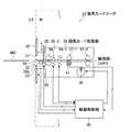
図1は、本発明の実施形態に係る磁気記録媒体処理装置としての磁気カードリーダの主要部の概略構成を示す図である。[Schematic configuration of magnetic card reader]
FIG. 1 is a diagram showing a schematic configuration of a main part of a magnetic card reader as a magnetic recording medium processing apparatus according to an embodiment of the present invention.
図1の磁気カードリーダ10は、装置の外部OTと内部INを仕切るフロントパネル20、フロントパネル20の内部側に固定された磁気ヘッド31を含む磁気カード処理部30、駆動制御部40、および基本的に、フロントパネル20の外部側の領域に妨害磁界を発生するように配置される磁界発生装置50を含んで構成されている。 A
なお、磁界発生装置(妨害磁界発生装置という場合もある)50は、回路構成等に特徴を有しており、その具体的な構成については、複数の実施形態を例に後で詳細に説明する。 The magnetic field generation device (sometimes referred to as a disturbing magnetic field generation device) 50 is characterized by a circuit configuration and the like, and the specific configuration will be described in detail later by taking a plurality of embodiments as an example. .
フロントパネル20には、磁気データが記録された磁気記録媒体としての磁気カードMCが挿入または排出されるカードスロット用開口21が形成されている。
そして、このカードスロット用開口21の内部側(裏面側)に磁気カード処理部30が固定されている。The
A magnetic card processing unit 30 is fixed to the inner side (back side) of the
磁気カード処理部30は、磁気カード挿入および排出用のカードスロット32、およびカードスロット32から挿入される磁気カードMCを検出するためのカード挿入検出用の磁気ヘッドであるプリヘッド33を有している。
さらに、磁気カード処理部30は、カードスロット32から挿入される磁気カードMCを内部に導く導入路34、およびこの導入路34を開閉するシャッター35を有している。
磁気カード処理部30においては、これらカードスロット32、プリヘッド33、導入路34、およびシャッター35が、カード挿入方向に沿って(装置の内部に向かって)、表記した順序で配置されている。The magnetic card processing unit 30 has a
Further, the magnetic card processing unit 30 has an
In the magnetic card processing unit 30, the
磁気カード処理部30において、シャッター35の奥(さらに内部)には、カード取込み排出ローラ対36が配置されている。
このカード取込み排出ローラ対36によって内部に取り込まれた磁気カードMCは、所定の間隔で配置されている複数組の搬送ローラ対37−1、37−2によって規定される搬送路CAPSに沿って搬送される。
各ローラ対36,37−1,37−2は、駆動制御部40の制御の下、駆動モータ38によって回転駆動される。
搬送ローラ対37−1の配置位置には、ここを通過する磁気カードMCに形成されている磁気ストライプに対して磁気的にデータを記録・再生するための磁気ヘッド31が配置されている。In the magnetic card processing unit 30, a card take-out /
The magnetic card MC taken in by the card take-out /
Each
A
磁気カード処理部30において、排出等される磁気カードMCの端部(たとえば後端部)を検出するためのフォトセンサ39−1,39−2が配置されている。 In the magnetic card processing unit 30, photosensors 39-1 and 39-2 for detecting an end (for example, a rear end) of the magnetic card MC to be ejected are arranged.
駆動制御部40は、各部の駆動制御を司り、マイクロコンピュータ等により構成することができ、その内蔵ROM内に格納されている制御プログラムに従って、磁気カードMCの搬送動作、磁気ヘッド31による読み取り動作等を制御する。 The
本実施形態に係る磁気カードリーダ10は、フロントパネル20に形成された開口21の内部側(裏面側)に、妨害磁界を発生する磁界発生装置50が配置されている。
すなわち、フロントパネル20における開口21が形成されている部位の裏面であって、磁気カード処理部30の装置フレーム30aの図中の下側(下部)に、妨害磁界発生装置50が取付けられている。
なお、磁界発生装置50の取り付け位置(配置位置)は、あくまでも一例であって、磁気カードの種類や装置構造等を考慮して、装置フレーム30aの上部等、適宜選択される。In the
That is, the disturbing magnetic
Note that the attachment position (arrangement position) of the magnetic
この妨害磁界発生装置50は、磁界を発生するためのインダクタL1を含んで構成されている。
インダクタL1は、たとえば図2(A)に示すように、コイルCLにより形成され、あるいは、インダクタL2は、図2(B)に示すように、鉄心FCにコイルCLを巻いて形成される。
磁界発生装置50は、駆動制御部40の制御の下に、コイルCLには交流あるいは直流電流が流される。電流が流されると、開口21あるいはカードスロット32の外側部分に妨害磁界が発生するように構成され、配置される。
妨害磁界の発生領域は、カードスロット32を介して挿入あるいは排出される磁気カードMCに形成されている磁気ストライプの通過領域を含む領域となるように構成されている。The disturbing
The inductor L1 is formed by a coil CL, for example, as shown in FIG. 2A, or the inductor L2 is formed by winding the coil CL around an iron core FC, as shown in FIG. 2B.
In the
The generation region of the disturbing magnetic field is configured to be a region including a passage region of a magnetic stripe formed on the magnetic card MC inserted or ejected through the
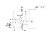
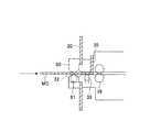
図3は、装置外部側に磁気ヘッドを含むスキマーが取り付けられた状態を模式的に示す図である。
図4は、装置外部側に磁気ヘッドを含むスキマーが取り付けられた状態の一例を具体的に示す図である。FIG. 3 is a diagram schematically showing a state in which a skimmer including a magnetic head is attached to the outside of the apparatus.
FIG. 4 is a diagram specifically illustrating an example of a state in which a skimmer including a magnetic head is attached to the outside of the apparatus.
磁気カードリーダ10では、磁気カードMCの挿入時には、その先端をカードスロット32に挿入されると同時に、磁気カードMCがカード取込み排出ローラ対36によって一定の速度で搬送される。
同様に、磁気カードの排出時にも、磁気カードMCがカードスロット32から実質的に外部に排出されるまでカード取込み排出ローラ対36によって一定の速度で搬送される。In the
Similarly, when the magnetic card is ejected, the magnetic card MC is conveyed at a constant speed by the card take-in /
したがって、カードスロット32の外部側に磁気ヘッド(スキミングヘッド)および磁気読み取り回路を含むスキマー(不正に磁気カードのデータを読み取る装置)を取り付けた場合には、スキミングヘッド(磁気ヘッド)に沿って、一定の速度で磁気カードが移動することになる。
このため、このようなカードスロットの外部側に取り付けた磁気ヘッドにより、磁気カードの記録データを読み取ることが可能である。Therefore, when a skimmer including a magnetic head (skimming head) and a magnetic reading circuit (an apparatus that illegally reads data on the magnetic card) is attached to the outside of the
For this reason, it is possible to read the recording data of the magnetic card by the magnetic head attached to the outside of the card slot.
本実施形態に係る磁気カードリーダ10においては、たとえば図3および図4に示すように、カードスロット用開口21が形成されているフロントパネル20の表面に不正に磁気ヘッド61を含むスキマー60が取り付けられたとしても、このような磁気ヘッド(スキミングヘッド)61による磁気カードMCの読み取り動作を、妨害磁界発生装置50による妨害磁界によって阻止することができる。 In the
ただし、最近のスキミングヘッドは、金属製のカバーが被せられている場合がある。
この金属カバーにより磁界発生装置による妨害磁界が防御され、妨害磁界が十分な効果を発揮し得ないことがある。
このため、不正行為者の読み取り回路が、磁界発生装置の周波数と出力を認識して解析し、妨害磁界による効果を消滅させ、磁気カードのデータを読み出す可能性がある。However, recent skimming heads may be covered with a metal cover.
This metal cover protects the disturbing magnetic field generated by the magnetic field generator, and the disturbing magnetic field may not be able to exert a sufficient effect.
For this reason, there is a possibility that the reading circuit of the fraudster recognizes and analyzes the frequency and output of the magnetic field generator, eliminates the effect of the disturbing magnetic field, and reads the data on the magnetic card.
そこで、本実施形態においては、妨害磁界の出力を増大させることが可能で、磁気データの不正取得を確実に防止することを可能とする、以下に説明するような特徴的な構成を有する磁界発生装置50が採用されている。 Therefore, in the present embodiment, it is possible to increase the output of the disturbing magnetic field, and it is possible to reliably prevent illegal acquisition of magnetic data, and to generate a magnetic field having a characteristic configuration as described below. A
[磁界発生装置50の構成例]
次に、妨害磁界を発生する磁界発生装置50の具体的な回路構成および動作を複数(第1〜第8)の実施形態として詳細に説明する。
以下に説明において、第1の本実施形態に係る磁界発生装置50Aは、基本的に、インダクタであるコイルに印加する電圧の供給を、コイルの一端側および他端側で交互に切り替えて交番磁界を発生する機能を有する。
この磁界発生装置50Aは、交番磁界を発生するで、妨害磁界の出力を結果的に増大させ、磁気データの不正取得を確実に防止することができる。[Configuration Example of Magnetic Field Generator 50]
Next, a specific circuit configuration and operation of the
In the following description, the
This
第2の実施形態に係る磁界発生装置50Bは、第1の実施形態の交番磁界の発生機能に加えて、コイルに印加する電圧の供給を、コイルの一端側および他端側で交互に切り替えるときに発生する回生電流を駆動電源部側に接続したキャパシタに充電して、インダクタであるコイルに印加される電圧を上げる機能を有する。
この磁界発生装置50Bは、妨害磁界の出力をさらに増大させることが可能となる。When the
This
第3の実施形態に係る磁界発生装置50Cは、第1および第2の実施形態の交番磁界の発生機能は備えていないが、回生電流を駆動電源部側に接続したキャパシタに充電して、インダクタであるコイルに印加される電圧を上げる機能を有する。
この磁界発生装置50Cは、妨害磁界の出力を増大させることが可能となる。The magnetic field generation device 50C according to the third embodiment does not have the function of generating the alternating magnetic field of the first and second embodiments, but charges a capacitor connected to the drive power supply unit side with a regenerative current to generate an inductor It has a function to increase the voltage applied to the coil.
This magnetic field generator 50C can increase the output of the disturbing magnetic field.
第4の実施形態に係る磁界発生装置50Dは、第1および第2の実施形態の交番磁界の発生機能、並びに第2および第3の実施形態の回線電流の充電機能は備えていないが、電源電圧を上げれば十分に不正行為を阻止可能な回路構成を有する。
第4の実施形態に係る磁界発生装置50Dは、基本的な回路を有している。The
The
[磁界発生装置の第1の実施形態]
まず、第1の実施形態に係る磁界発生装置について説明する。
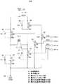
図5は、本発明の第1の実施形態に係る磁界発生装置を示す回路図である。[First Embodiment of Magnetic Field Generator]
First, the magnetic field generator according to the first embodiment will be described.
FIG. 5 is a circuit diagram showing the magnetic field generator according to the first embodiment of the present invention.
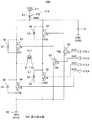
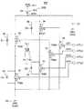
図5の磁界発生装置50Aは、基本的に、磁界を発生するためのインダクタL1としてのコイルCL1、駆動電源電圧VCCを供給する駆動電源部51、および基準電位部52を有する。
本実施形態においては、駆動電源部51が供給する駆動電源電圧VCCは、12Vあるいは20Vに設定される。
駆動電源部51は、各素子と接続される接続ノードND51を通して駆動電源電圧VCCを供給する。
また、基準電位部52は、基準電位VSSに設定される。本実施形態において、基準電位は接地電位GNDである。The
In the present embodiment, the drive power supply voltage VCC supplied by the drive
The drive
The reference
さらに、磁界発生装置50Aは、相補的に導通状態または非導通状態となるように駆動制御部40により制御される、第1のスイッチング部53および第2のスイッチング部54を有する。
ここで、相補的とは、第1のスイッチング部53が導通状態(ON状態)のときは第2のスイッチング部54が非導通状態(OFF状態)となり、第1のスイッチング部53が非導通状態(OFF状態)のときは第2のスイッチング部54が導通状態(ON状態)となることをいう。Furthermore, the
Here, complementary means that when the
第1のスイッチング部53は、導通状態となるように制御されたときは、インダクタであるコイルCL1の一端T1を駆動電源部51側の接続ノードND51に接続し、他端T2を基準電位部52の接地電位GNDに接続する。
第1のスイッチング部53は、非導通状態となるように制御されたときは、インダクタであるコイルCL1の一端T1と駆動電源部51側の接続ノードND51を電気的に切り離しに、他端T2と基準電位部52の接地電位GNDとを電気的に切り離す。When the
When the
第1のスイッチング部53は、インダクタであるコイルCL1の一端T1と駆動電源部51側の接続ノードND51との間に接続された第1のスイッチング素子としてのpnp型の第1のトランジスタTR1を有する。
第1のスイッチング部53は、コイルCL1の他端T2と基準電位部52の接地電位GNDとの間に接続された第2のスイッチング素子としてのnpn型の第2のトランジスタTR2を有する。
さらに、第1のスイッチング部53は、第1のトランジスタTR1のベースと接地電位GNDとの間に接続された第5のスイッチング素子としてのnpn型の第5のトランジスタTR5を有する。The
The
Furthermore, the
具体的には、第1のトランジスタTR1のエミッタが接続ノードND51に接続され、コレクタがコイルCL1の一端T1に接続され、ベースが第5のトランジスタTR5のコレクタに接続されている。
第2のトランジスタTR2のコレクタがコイルCL1の他端T2に接続され、エミッタが基準電位部52の接地電位GNDに接続されている。
第5のトランジスタTR5のエミッタが接地電位GNDに接続されている。
そして、第5のトランジスタTR5のベースがドライバDV2を介して駆動制御部40による制御信号CTL2の供給ラインに接続されている。
第2のトランジスタTR2のベースがドライバDV3を介して駆動制御部40による制御信号CTL3の供給ラインに接続されている。
制御信号CTL2およびCTL3は、同相の信号であり、npn型トランジスタである第5のトランジスタTR5と第2のトランジスタTR2をオン(ON)状態とするハイレベル(H)と、オフ(OFF)状態にするローレベル(L)とが交互に切り替えられる信号として供給される。Specifically, the emitter of the first transistor TR1 is connected to the connection node ND51, the collector is connected to one end T1 of the coil CL1, and the base is connected to the collector of the fifth transistor TR5.
The collector of the second transistor TR2 is connected to the other end T2 of the coil CL1, and the emitter is connected to the ground potential GND of the reference
The emitter of the fifth transistor TR5 is connected to the ground potential GND.
The base of the fifth transistor TR5 is connected to the supply line of the control signal CTL2 from the
The base of the second transistor TR2 is connected to the supply line of the control signal CTL3 from the
The control signals CTL2 and CTL3 are in-phase signals, and are in a high level (H) for turning on the fifth transistor TR5 and the second transistor TR2 which are npn transistors, and in an off (OFF) state. The low level (L) to be supplied is supplied as a signal that can be switched alternately.
第2のスイッチング部54は、導通状態となるように制御されたときは、インダクタであるコイルCL1の他端T2を駆動電源部51側の接続ノードND51に接続し、一端T1を基準電位部52の接地電位GNDに接続する。
第1のスイッチング部53は、非導通状態となるように制御されたときは、インダクタであるコイルCL1の他端T2と駆動電源部51側の接続ノードND51を電気的に切り離しに、一端T1と基準電位部52の接地電位GNDとを電気的に切り離す。When the
When the
第2のスイッチング部54は、インダクタであるコイルCL1の他端T2と駆動電源部51側の接続ノードND51との間に接続された第3のスイッチング素子としてのpnp型の第3のトランジスタTR3を有する。
第2のスイッチング部54は、コイルCL1の一端T1と基準電位部52の接地電位GNDとの間に接続された第4のスイッチング素子としてのnpn型の第4のトランジスタTR4を有する。
さらに、第2のスイッチング部54は、第3のトランジスタTR3のベースと接地電位GNDとの間に接続された第6のスイッチング素子としてのnpn型の第6のトランジスタTR6を有する。The
The
Further, the
具体的には、第3のトランジスタTR3のエミッタが接続ノードND51に接続され、コレクタがコイルCL1の他端T2に接続され、ベースが第6のトランジスタTR6のコレクタに接続されている。
第4のトランジスタTR4のコレクタがコイルCL1の一端T1に接続され、エミッタが基準電位部52の接地電位GNDに接続されている。
第6のトランジスタTR6のエミッタが接地電位GNDに接続されている。
そして、第6のトランジスタTR6のベースがドライバDV1を介して駆動制御部40による制御信号CTL1の供給ラインに接続されている。
第4のトランジスタTR4のベースがドライバDV4を介して駆動制御部40による制御信号CTL4の供給ラインに接続されている。
制御信号CTL1およびCTL4は、同相の信号であり、npn型トランジスタである第6のトランジスタTR6と第4のトランジスタTR4をオン(ON)状態とするハイレベル(H)と、オフ(OFF)状態にするローレベル(L)とが交互に切り替えられる信号として供給される。Specifically, the emitter of the third transistor TR3 is connected to the connection node ND51, the collector is connected to the other end T2 of the coil CL1, and the base is connected to the collector of the sixth transistor TR6.
The collector of the fourth transistor TR4 is connected to one end T1 of the coil CL1, and the emitter is connected to the ground potential GND of the reference
The emitter of the sixth transistor TR6 is connected to the ground potential GND.
The base of the sixth transistor TR6 is connected to the supply line of the control signal CTL1 from the
The base of the fourth transistor TR4 is connected to the supply line of the control signal CTL4 by the
The control signals CTL1 and CTL4 are in-phase signals, and are in the high level (H) that turns on the sixth transistor TR6 and the fourth transistor TR4, which are npn transistors, and in the off (OFF) state. The low level (L) to be supplied is supplied as a signal that can be switched alternately.
そして、第1のスイッチング部53の導通状態を制御する制御信号CTL2およびCTL3と、第2のスイッチング部54の導通状態を制御する制御信号CTL1およびCTL4は、相補的なレベルをとる。
具体的には、制御信号CTL2およびCTL3がハイレベル(H)をとるときは、制御信号CTL1およびCTL4はローレベル(L)をとり、制御信号CTL2およびCTL3がローレベル(L)をとるときは、制御信号CTL1およびCTL4はハイレベル(H)をとる。The control signals CTL2 and CTL3 that control the conduction state of the
Specifically, when the control signals CTL2 and CTL3 take a high level (H), the control signals CTL1 and CTL4 take a low level (L), and when the control signals CTL2 and CTL3 take a low level (L) The control signals CTL1 and CTL4 take a high level (H).
さらに、磁界発生装置50Aは、基準電位部52の接地電位GND側からコイルCL1を介して駆動電源部51に向かう回生電流(逆起電流、逆流する電力)がたどる電流経路を形成する第1の回生電流経路形成部55および第2の回生電流経路形成部56を有する。 Furthermore, the magnetic
第1の回生電流経路形成部55は、第1のスイッチング部53が非導通状態と導通状態が切り替わったとき、たとえば非導通状態から導通状態となったときに、回生電流の経路を、基準電位部52の接地電位GND、インダクタであるコイルCL1の他端T2、コイル(インダクタ)CL1、コイルCL1の一端T1、接続ノードND51、駆動電源部51の順にたどるように形成する。 The first regenerative current
第1の回生電流経路形成部55は、第1のダイオードD1および第2のダイオードD2を含んで構成されている。 The first regenerative current
第1のダイオードD1は、コイル(インダクタ)CL1の一端と駆動電源部51の接続ノードND51との間に第1のトランジスタ(第1のスイッチング素子)TR1と並列に、コイルCL1の一端T1から駆動電源部51に向かって順方向となるように接続されている。
すなわち、第1のダイオードD1は、アノードがコイルCL1の一端T1(および第1のトランジスタTR1のコレクタ)に接続され、カソードが接続ノードND51(および第1のトランジスタTR1のエミッタ)に接続されている。The first diode D1 is driven from one end T1 of the coil CL1 in parallel with the first transistor (first switching element) TR1 between one end of the coil (inductor) CL1 and the connection node ND51 of the driving
That is, the first diode D1 has an anode connected to one end T1 of the coil CL1 (and the collector of the first transistor TR1), and a cathode connected to the connection node ND51 (and the emitter of the first transistor TR1). .
第2のダイオードD2は、コイル(インダクタ)CL1の他端T2と基準電位部52の接地電位GNDとの間に第2のトランジスタ(第2のスイッチング素子)TR2と並列に、基準電位部52の接地電位GNDからコイルCL1の他端T2に向かって順方向となるように接続されている。
すなわち、第2のダイオードD2は、アノードが接地電位GND(および第2のトランジスタTR2のエミッタ)に接続され、カソードがコイルCL1の他端T2(および第2のトランジスタTR2のコレクタ)に接続されている。The second diode D2 is connected between the other end T2 of the coil (inductor) CL1 and the ground potential GND of the reference
That is, the second diode D2 has an anode connected to the ground potential GND (and the emitter of the second transistor TR2) and a cathode connected to the other end T2 of the coil CL1 (and the collector of the second transistor TR2). Yes.
第2の回生電流経路形成部56は、第2のスイッチング部54が非導通状態と導通状態が切り替わったとき、たとえば非導通状態から導通状態となったときに、回生電流の経路を、基準電位部52の接地電位GND、コイル(インダクタ)CL1の一端T1、コイル(インダクタ)CL1、コイルCL1の他端T2、接続ノードND51、駆動電源部51の順にたどるように形成する。 The second regenerative current
第2の回生電流経路形成部56は、第3のダイオードD3および第4のダイオードD4を含んで構成されている。 The second regenerative current
第3のダイオードD3は、コイル(インダクタ)CL1の他端T2と駆動電源部51の接続ノードND51との間に第3のトランジスタ(第3のスイッチング素子)TR3と並列に、コイルCL1の他端T2から駆動電源部51に向かって順方向となるように接続されている。
すなわち、第3のダイオードD3は、アノードがコイルCL1の他端T2(および第3のトランジスタTR3のコレクタ)に接続され、カソードが接続ノードND51(および第3のトランジスタTR3のエミッタ)に接続されている。The third diode D3 is connected to the other end of the coil CL1 in parallel with the third transistor (third switching element) TR3 between the other end T2 of the coil (inductor) CL1 and the connection node ND51 of the drive
That is, the third diode D3 has an anode connected to the other end T2 of the coil CL1 (and the collector of the third transistor TR3) and a cathode connected to the connection node ND51 (and the emitter of the third transistor TR3). Yes.
第4のダイオードD4は、コイル(インダクタ)CL1の一端T1と基準電位部の接地電位GNDとの間に第4のトランジスタ(第4のスイッチング素子)TR4と並列に、基準電位部52の接地電位GNDからコイルCL1の一端T1に向かって順方向となるように接続されている。
すなわち、第4のダイオードD4は、アノードが接地電位GND(および第4のトランジスタTR4のエミッタ)に接続され、カソードがコイルCL1の一端T1(および第4のトランジスタTR4のコレクタ)に接続されている。The fourth diode D4 is connected between the one end T1 of the coil (inductor) CL1 and the ground potential GND of the reference potential portion in parallel with the fourth transistor (fourth switching element) TR4, and is connected to the ground potential of the reference
That is, the fourth diode D4 has an anode connected to the ground potential GND (and the emitter of the fourth transistor TR4) and a cathode connected to one end T1 of the coil CL1 (and the collector of the fourth transistor TR4). .
以上の構成を有する電界発生装置50Aは、等価回路としては、インダクタであるコイルCL1がブリッジの機能を果たすいわゆるH型の回路を形成しており、この回路をHブリッジ回路としていうこともできる。
また、回路配置としては、図1に示すように、フロントパネル20の内部側(裏面側)近傍に電界発生装置50Aを、全体回路を含んで配置することができるが、たとえばコイル(インダクタ)CL1のみフロントパネル20の内部側近傍に配置し、残りの回路系を他の位置、たとえば駆動制御部40側に配置する等、種々の態様が可能である。In the
Further, as a circuit arrangement, as shown in FIG. 1, the
次に、第1の実施形態に係る磁界発生装置50Aの動作を、図6〜図11に関連付けて説明する。
なお、以下の説明では、第1のスイッチング部53を導通状態としてコイル(インダクタ)CL1の一端T1側に電圧を印加する(入れる)ことを正方向駆動(正方向動作)、第2のスイッチング部54を導通状態として他端T2側に印加する(入れる)ことを逆方向駆動(逆方向動作)として説明する。Next, the operation of the
In the following description, applying the
まず、正方向動作を行うように制御信号CTL1〜CT4が駆動制御部40から供給される。
この場合、図6に示すように、制御信号CTL2とCTL3がハイレベル(H)で供給され、制御信号CTL1とCTL4がローレベル(L)で供給される。
これに伴い、第2のトランジスタTR2および第5のトランジスタTR5が導通状態(ON状態)となり、第3のトランジスタTR3および第4のトランジスタTR4が非導通状態(OFF状態)に保持される。
第5のトランジスタTR5がON状態となったことに伴い、第1のトランジスタTR1のベース電位が接地電位GNDに向かって下がり、第1のトランジスタTR1がON状態となる。
すなわち、正方向動作においては、第1のスイッチング部53がON状態となり、第2のスイッチング部54がOFF状態に保持される。
これにより、図6中に矢印XDで示すように、駆動電源部51の駆動電源電位部511、第1のトランジスタTR1、コイルCL1の一端T1、コイルCL1、コイルCL1の他端T2、第2のトランジスタTR2、基準電位部52の接地電位GNDの順にたどる駆動経路が形成される。
これに伴い、コイルCL1の一端T1から他端T2へ電流が流れ、コイルCL1から妨害磁界が発生する。First, the control signals CTL1 to CT4 are supplied from the
In this case, as shown in FIG. 6, the control signals CTL2 and CTL3 are supplied at a high level (H), and the control signals CTL1 and CTL4 are supplied at a low level (L).
Accordingly, the second transistor TR2 and the fifth transistor TR5 are turned on (ON state), and the third transistor TR3 and the fourth transistor TR4 are held in a non-conductive state (OFF state).
As the fifth transistor TR5 is turned on, the base potential of the first transistor TR1 decreases toward the ground potential GND, and the first transistor TR1 is turned on.
That is, in the forward direction operation, the
Accordingly, as indicated by an arrow XD in FIG. 6, the drive power supply
Along with this, a current flows from one end T1 to the other end T2 of the coil CL1, and a disturbing magnetic field is generated from the coil CL1.
次に、逆方向動作を行うように制御信号CTL1〜CT4が駆動制御部40から供給される。
この場合、図7および図8に示すように、制御信号CTL1とCTL4がハイレベル(H)で供給され、制御信号CTL2とCTL3がローレベル(L)で供給される。
これに伴い、第4のトランジスタTR4および第6のトランジスタTR6がON状態となり、第2のトランジスタTR2、第5のトランジスタTR5、および第1のトランジスタTR1がOFF状態となる。
第6のトランジスタTR6がON状態となったことに伴い、第3のトランジスタTR3のベース電位が接地電位GNDに向かって下がり、第3のトランジスタTR3がON状態となる。
すなわち、逆方向動作においては、第2のスイッチング部54がOFF状態からON状態に切り替わり、第1のスイッチング部53がON状態からOFF状態に切り替わる。
このとき、ON状態となる第3のトランジスタTR3および第4のトランジスタTR4は通電の始まりの状態にある。
第2のスイッチング部54がOFF状態からON状態に切り替わったとき、図7中に矢印YIで示すように、回生電流(逆起電流)の経路が、基準電位部52の接地電位GND、第4のダイオードD4、コイル(インダクタ)CL1の一端T1、コイル(インダクタ)CL1、コイルCL1の他端T2、第3のダイオードD3、駆動電源部51の駆動電源電位部511の順にたどるように形成される。
この経路をたどって回生電流が流れ、駆動電源電位部511から回路(本磁界発生装置50A)の外部に流れ出す。Next, control signals CTL <b> 1 to CT <b> 4 are supplied from the
In this case, as shown in FIGS. 7 and 8, the control signals CTL1 and CTL4 are supplied at a high level (H), and the control signals CTL2 and CTL3 are supplied at a low level (L).
Accordingly, the fourth transistor TR4 and the sixth transistor TR6 are turned on, and the second transistor TR2, the fifth transistor TR5, and the first transistor TR1 are turned off.
As the sixth transistor TR6 is turned on, the base potential of the third transistor TR3 decreases toward the ground potential GND, and the third transistor TR3 is turned on.
That is, in the reverse operation, the
At this time, the third transistor TR3 and the fourth transistor TR4 that are in the ON state are in a state of starting energization.
When the
A regenerative current flows along this path, and flows out from the drive power supply
これにより、コイルCL1が発生する磁界が弱くなり、コイルCL1の一端T1から他端T2への回生電流の流れが納まる。
そして、図8中に矢印YDで示すように、駆動電源部51の駆動電源電位部511、第3のトランジスタTR3、コイルCL1の他端T2、コイルCL1、コイルCL1の一端T1、第4のトランジスタTR4、基準電位部52の接地電位GNDの順にたどる駆動経路が形成される。
これに伴い、コイルCL1の他端T2から一端T1へ電流が流れ、コイルCL1から正方向駆動とは逆のいわゆる逆方向の妨害磁界が発生する。Thereby, the magnetic field generated by the coil CL1 becomes weak, and the flow of the regenerative current from one end T1 to the other end T2 of the coil CL1 is stopped.
Then, as indicated by an arrow YD in FIG. 8, the drive power supply
Along with this, a current flows from the other end T2 of the coil CL1 to the one end T1, and a so-called reverse disturbing magnetic field is generated from the coil CL1 opposite to the forward driving.
次に、正方向動作を行うように制御信号CTL1〜CT4が駆動制御部40から供給される。
この場合、図9および図10に示すように、制御信号CTL2とCTL3がハイレベル(H)で供給され、制御信号CTL1とCTL4がローレベル(L)で供給される。
これに伴い、第1のトランジスタTR1および第5のトランジスタTR5がON状態となり、第4のトランジスタTR4、第6のトランジスタTRF6、および第3のトランジスタTR3がOFF状態となる。
第5のトランジスタTR5がON状態となったことに伴い、第1のトランジスタTR1のベース電位が接地電位GNDに向かって下がり、第1のトランジスタTR1がON状態となる。
すなわち、正方向動作においては、第1のスイッチング部53がOFF状態からON状態に切り替わり、第2のスイッチング部54がON状態からOFF状態に切り替わる。
このとき、ON状態となる第1のトランジスタTR1および第2のトランジスタTR2は通電の始まりの状態にある。
第1のスイッチング部53がOFF状態からON状態に切り替わったとき、図9中に矢印XIで示すように、回生電流(逆起電流)の経路が、基準電位部52の接地電位GND、第2のダイオードD2、コイル(インダクタ)CL1の他端T2、コイル(インダクタ)CL1、コイルCL1の一端T1、第1のダイオードD1、駆動電源部51の駆動電源電位部511の順にたどるように形成される。
この経路をたどって回生電流が流れ、駆動電源電位部511から回路(本磁界発生装置50A)の外部に流れ出す。Next, control signals CTL <b> 1 to CT <b> 4 are supplied from the
In this case, as shown in FIGS. 9 and 10, the control signals CTL2 and CTL3 are supplied at a high level (H), and the control signals CTL1 and CTL4 are supplied at a low level (L).
Accordingly, the first transistor TR1 and the fifth transistor TR5 are turned on, and the fourth transistor TR4, the sixth transistor TRF6, and the third transistor TR3 are turned off.
As the fifth transistor TR5 is turned on, the base potential of the first transistor TR1 decreases toward the ground potential GND, and the first transistor TR1 is turned on.
That is, in the forward operation, the
At this time, the first transistor TR1 and the second transistor TR2 that are in the ON state are in a state of starting energization.
When the
A regenerative current flows along this path, and flows out from the drive power supply
これにより、コイルCL1が発生する磁界が弱くなり、コイルCL1の他端T2から一端T1への回生電流の流れが納まる。
そして、図10中に矢印XDで示すように、駆動電源部51の駆動電源電位部511、第1のトランジスタTR1、コイルCL1の一端T1、コイルCL1、コイルCL1の他端T2、第2のトランジスタTR2、基準電位部52の接地電位GNDの順にたどる駆動経路が形成される。
これに伴い、コイルCL1の一端T1から他端T2へ電流が流れ、コイルCL1から逆方向駆動とは逆のいわゆる正方向の妨害磁界が発生する。Thereby, the magnetic field generated by the coil CL1 becomes weak, and the flow of the regenerative current from the other end T2 to the one end T1 of the coil CL1 is stopped.
Then, as indicated by an arrow XD in FIG. 10, the drive power supply
Along with this, a current flows from one end T1 to the other end T2 of the coil CL1, and a so-called forward disturbing magnetic field reverse to reverse driving is generated from the coil CL1.
次に、逆方向動作を行うように制御信号CTL1〜CT4が駆動制御部40から供給される。
この場合、図11に示すように、制御信号CTL1とCTL4がハイレベル(H)で供給され、制御信号CTL2とCTL3がローレベル(L)で供給される。
これに伴い、第4のトランジスタTR4および第6のトランジスタTR6がON状態となり、第2のトランジスタTR2、第5のトランジスタTR5、および第1のトランジスタTR1がOFF状態となる。
第6のトランジスタTR6がON状態となったことに伴い、第3のトランジスタTR3のベース電位が接地電位GNDに向かって下がり、第3のトランジスタTR3がON状態となる。
すなわち、逆方向動作においては、第2のスイッチング部54がOFF状態からON状態に切り替わり、第1のスイッチング部53がON状態からOFF状態に切り替わる。
このとき、ON状態となる第3のトランジスタTR3および第4のトランジスタTR4は通電の始まりの状態にある。
第2のスイッチング部54がOFF状態からON状態に切り替わったとき、図11中に矢印YIで示すように、回生電流(逆起電流)の経路が、基準電位部52の接地電位GND、第4のダイオードD4、コイル(インダクタ)CL1の一端T1、コイル(インダクタ)CL1、コイルCL1の他端T2、第3のダイオードD3、駆動電源部51の駆動電源電位部511の順にたどるように形成される。
この経路をたどって回生電流が流れ、駆動電源電位部511から回路(本磁界発生装置50A)の外部に流れ出す。Next, control signals CTL <b> 1 to CT <b> 4 are supplied from the
In this case, as shown in FIG. 11, the control signals CTL1 and CTL4 are supplied at a high level (H), and the control signals CTL2 and CTL3 are supplied at a low level (L).
Accordingly, the fourth transistor TR4 and the sixth transistor TR6 are turned on, and the second transistor TR2, the fifth transistor TR5, and the first transistor TR1 are turned off.
As the sixth transistor TR6 is turned on, the base potential of the third transistor TR3 decreases toward the ground potential GND, and the third transistor TR3 is turned on.
That is, in the reverse operation, the
At this time, the third transistor TR3 and the fourth transistor TR4 that are in the ON state are in a state of starting energization.
When the
A regenerative current flows along this path, and flows out from the drive power supply
これにより、コイルCL1が発生する磁界が弱くなり、コイルCL1の一端T1から他端T2への回生電流の流れが納まる。
そして、上記した図8中に矢印YDで示すように、駆動電源部51の駆動電源電位部511、第2のトランジスタTR2、コイルCL1の他端T2、コイルCL1、コイルCL1の一端T1、第4のトランジスタTR4、基準電位部52の接地電位GNDの順にたどる駆動経路が形成される。
これに伴い、コイルCL1の他端T2から一端T1へ電流が流れ、コイルCL1から正方向駆動とは逆のいわゆる逆方向の妨害磁界が発生する。Thereby, the magnetic field generated by the coil CL1 becomes weak, and the flow of the regenerative current from one end T1 to the other end T2 of the coil CL1 is stopped.
Then, as indicated by the arrow YD in FIG. 8 described above, the drive power supply
Along with this, a current flows from the other end T2 of the coil CL1 to the one end T1, and a so-called reverse disturbing magnetic field is generated from the coil CL1 opposite to the forward driving.
以上のようにして、正方向駆動と逆方向駆動が交互に行われ、交番磁界が発生され、妨害磁界の出力を結果的に増大させ、磁気データの不正取得を確実に防止することができる。
すなわち、不正行為者が、磁気カードの磁気データを読み取るために、フロントパネルの外部側に、カードリーダのカード挿入口に、磁気ヘッド(スキミングヘッド)と磁気読み取り回路を含むいわゆるスキマー60を取り付けていたとしても、交番磁界を発生することが可能で、妨害磁界の出力を増大させ、磁気データの不正取得を確実に防止することができる。As described above, the forward drive and the reverse drive are alternately performed, an alternating magnetic field is generated, the output of the disturbing magnetic field is increased as a result, and illegal acquisition of magnetic data can be reliably prevented.
That is, in order to read the magnetic data of the magnetic card, a fraudulent person attaches a so-called
[磁界発生装置の第2の実施形態]
次に、第2の実施形態に係る磁界発生装置について説明する。
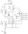
図12は、本発明の第2の実施形態に係る磁界発生装置を示す回路図である。[Second Embodiment of Magnetic Field Generator]
Next, a magnetic field generator according to the second embodiment will be described.
FIG. 12 is a circuit diagram showing a magnetic field generator according to the second embodiment of the present invention.
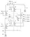
本第2の実施形態に係る磁界発生装置50Bが上述した第1の実施形態に係る磁界発生装置50Aと異なる点は、次の通りである。
磁界発生装置50Bは磁界発生装置50Aの構成に加えて、接続ノードND51と基準電位部の接地電位との間に接続されたキャパシタC1を有する。
さらに、磁界発生装置50Bは、駆動電源部51Bにおいて、接続ノードN51から回生電流の流入を阻止する流入阻止部512が配置されている。
流入阻止部512は、駆動電源電位部511と接続ノードND51との間に、駆動電源電位部511から接続ノードND51に向かって順方向となるように接続された第5のダイオードD5を含む。
すなわち、第5のダイオードD5のアノードが駆動電源電位部511に接続され、カソードが接続ノードND51に接続されている。The
In addition to the configuration of the
Furthermore, in the
That is, the anode of the fifth diode D5 is connected to the drive power supply
このように、第2の実施形態に係る磁界発生装置50Bは、第1の実施形態の交番磁界の発生機能に加えて、コイルに印加する電圧の供給を、コイルの一端側および他端側で交互に切り替えるときに発生する回生電流を駆動電源部側に接続したキャパシタC1に充電して、インダクタであるコイルCL1に印加される電圧を上げる機能を有する。
この磁界発生装置50Bは、妨害磁界の出力をさらに増大させることが可能となる。Thus, in addition to the alternating magnetic field generating function of the first embodiment, the
This
次に、第2の実施形態に係る磁界発生装置50Bの動作を、図13〜図18に関連付けて説明する。 Next, the operation of the
まず、正方向動作を行うように制御信号CTL1〜CT4が駆動制御部40から供給される。
この場合、図13に示すように、制御信号CTL2とCTL3がハイレベル(H)で供給され、制御信号CTL1とCTL4がローレベル(L)で供給される。
これに伴い、第2のトランジスタTR2および第5のトランジスタTR5が導通状態(ON状態)となり、第3のトランジスタTR3および第4のトランジスタTR4が非導通状態(OFF状態)に保持される。
第5のトランジスタTR5がON状態となったことに伴い、第1のトランジスタTR1のベース電位が接地電位GNDに向かって下がり、第1のトランジスタTR1がON状態となる。
すなわち、正方向動作においては、第1のスイッチング部53がON状態となり、第2のスイッチング部54がOFF状態に保持される。
これにより、図13中に矢印XDで示すように、駆動電源部51の駆動電源電位部511、第5のダイオードD5、第1のトランジスタTR1、コイルCL1の一端T1、コイルCL1、コイルCL1の他端T2、第2のトランジスタTR2、基準電位部52の接地電位GNDの順にたどる駆動経路が形成される。
これに伴い、コイルCL1の一端T1から他端T2へ電流が流れ、コイルCL1から妨害磁界が発生する。
またこのとき、駆動電源部51BによりキャパシタC1が、たとえば電源電圧VCCのレベル、たとえば12V(あるいは20V)に充電される。First, the control signals CTL1 to CT4 are supplied from the
In this case, as shown in FIG. 13, the control signals CTL2 and CTL3 are supplied at a high level (H), and the control signals CTL1 and CTL4 are supplied at a low level (L).
Accordingly, the second transistor TR2 and the fifth transistor TR5 are turned on (ON state), and the third transistor TR3 and the fourth transistor TR4 are held in a non-conductive state (OFF state).
As the fifth transistor TR5 is turned on, the base potential of the first transistor TR1 decreases toward the ground potential GND, and the first transistor TR1 is turned on.
That is, in the forward direction operation, the
Accordingly, as indicated by an arrow XD in FIG. 13, the drive power supply
Along with this, a current flows from one end T1 to the other end T2 of the coil CL1, and a disturbing magnetic field is generated from the coil CL1.
At this time, the capacitor C1 is charged to the level of the power supply voltage VCC, for example, 12V (or 20V) by the drive
次に、逆方向動作を行うように制御信号CTL1〜CT4が駆動制御部40から供給される。
この場合、図14および図15に示すように、制御信号CTL1とCTL4がハイレベル(H)で供給され、制御信号CTL2とCTL3がローレベル(L)で供給される。
これに伴い、第4のトランジスタTR4および第6のトランジスタTR6がON状態となり、第2のトランジスタTR2、第5のトランジスタTR5、および第1のトランジスタTR1がOFF状態となる。
第6のトランジスタTR6がON状態となったことに伴い、第3のトランジスタTR3のベース電位が接地電位GNDに向かって下がり、第3のトランジスタTR3がON状態となる。
すなわち、逆方向動作においては、第2のスイッチング部54がOFF状態からON状態に切り替わり、第1のスイッチング部53がON状態からOFF状態に切り替わる。
このとき、ON状態となる第3のトランジスタTR3および第4のトランジスタTR4は通電の始まりの状態にある。
第2のスイッチング部54がOFF状態からON状態に切り替わったとき、図14中に矢印YI2で示すように、回生電流(逆起電流)の経路が、基準電位部52の接地電位GND、第4のダイオードD4、コイル(インダクタ)CL1の一端T1、コイル(インダクタ)CL1、コイルCL1の他端T2、第3のダイオードD3、キャパシタC1の順にたどるように形成される。
このとき、駆動電源部51の駆動電源電位部511への回生電流の流入は流入阻止部512の第5のダイオードD5で阻止される。
この形成された経路をたどって回生電流が流れ、キャパシタC1に流れ込む。この流れ込んだ回生電流によりキャパシタC1は電源電圧VCC、たとえば12V(あるいは20V)より高い電圧、たとえば20V(あるいは30V)となるように充電される。Next, control signals CTL <b> 1 to CT <b> 4 are supplied from the
In this case, as shown in FIGS. 14 and 15, the control signals CTL1 and CTL4 are supplied at a high level (H), and the control signals CTL2 and CTL3 are supplied at a low level (L).
Accordingly, the fourth transistor TR4 and the sixth transistor TR6 are turned on, and the second transistor TR2, the fifth transistor TR5, and the first transistor TR1 are turned off.
As the sixth transistor TR6 is turned on, the base potential of the third transistor TR3 decreases toward the ground potential GND, and the third transistor TR3 is turned on.
That is, in the reverse operation, the
At this time, the third transistor TR3 and the fourth transistor TR4 that are in the ON state are in a state of starting energization.
When the
At this time, the inflow of the regenerative current to the drive power supply
A regenerative current flows along the formed path and flows into the capacitor C1. Due to the regenerative current that has flown in, the capacitor C1 is charged to a voltage higher than the power supply voltage VCC, eg, 12V (or 20V), for example, 20V (or 30V).
これにより、コイルCL1が発生する磁界が弱くなり、コイルCL1の一端T1から他端T2への回生電流の流れが納まる。
そして、図15中に矢印YD2で示すように、駆動電源部51の駆動電源電位部511並びにキャパシタC1、第3のトランジスタTR3、コイルCL1の他端T2、コイルCL1、コイルCL1の一端T1、第4のトランジスタTR4、基準電位部52の接地電位GNDの順にたどる駆動経路が形成される。
これに伴い、コイルCL1の他端T2から一端T1へ電流が流れ、コイルCL1から正方向駆動とは逆のいわゆる逆方向の妨害磁界が発生する。
このとき、コイルCL1に印加される(かかる)電圧が通常の電源電圧VCCより高い20Vや30Vに昇圧されていることから、コイルCL1に流れる電流も通常より大きくなり、妨害磁界の出力が、第1の実施形態ときよりもさらに増大されている(強くなっている)。Thereby, the magnetic field generated by the coil CL1 becomes weak, and the flow of the regenerative current from one end T1 to the other end T2 of the coil CL1 is stopped.
Then, as indicated by an arrow YD2 in FIG. 15, the drive power supply
Along with this, a current flows from the other end T2 of the coil CL1 to the one end T1, and a so-called reverse disturbing magnetic field is generated from the coil CL1 opposite to the forward driving.
At this time, since the voltage applied (applied) to the coil CL1 is boosted to 20V or 30V higher than the normal power supply voltage VCC, the current flowing through the coil CL1 becomes larger than usual, and the output of the disturbing magnetic field is It is further increased (stronger) than in the first embodiment.
次に、正方向動作を行うように制御信号CTL1〜CT4が駆動制御部40から供給される。
この場合、図16および図17に示すように、制御信号CTL2とCTL3がハイレベル(H)で供給され、制御信号CTL1とCTL4がローレベル(L)で供給される。
これに伴い、第1のトランジスタTR1および第5のトランジスタTR5がON状態となり、第4のトランジスタTR4、第6のトランジスタTRF6、および第3のトランジスタTR3がOFF状態となる。
第5のトランジスタTR5がON状態となったことに伴い、第1のトランジスタTR1のベース電位が接地電位GNDに向かって下がり、第1のトランジスタTR1がON状態となる。
すなわち、正方向動作においては、第1のスイッチング部53がOFF状態からON状態に切り替わり、第2のスイッチング部54がON状態からOFF状態に切り替わる。
このとき、ON状態となる第1のトランジスタTR1および第2のトランジスタTR2は通電の始まりの状態にある。
第1のスイッチング部53がOFF状態からON状態に切り替わったとき、図16中に矢印XI2で示すように、回生電流(逆起電流)の経路が、基準電位部52の接地電位GND、第2のダイオードD2、コイル(インダクタ)CL1の他端T2、コイル(インダクタ)CL1、コイルCL1の一端T1、第1のダイオードD1、キャパシタC1の順にたどるように形成される。
このとき、駆動電源部51の駆動電源電位部511への回生電流の流入は流入阻止部512の第5のダイオードD5で阻止される。
この形成された経路をたどって回生電流が流れ、キャパシタC1に流れ込む。この流れ込んだ回生電流によりキャパシタC1は電源電圧VCC、たとえば12V(あるいは20V)より高い電圧、たとえば20V(あるいは30V)となるように充電される。Next, control signals CTL <b> 1 to CT <b> 4 are supplied from the
In this case, as shown in FIGS. 16 and 17, the control signals CTL2 and CTL3 are supplied at a high level (H), and the control signals CTL1 and CTL4 are supplied at a low level (L).
Accordingly, the first transistor TR1 and the fifth transistor TR5 are turned on, and the fourth transistor TR4, the sixth transistor TRF6, and the third transistor TR3 are turned off.
As the fifth transistor TR5 is turned on, the base potential of the first transistor TR1 decreases toward the ground potential GND, and the first transistor TR1 is turned on.
That is, in the forward operation, the
At this time, the first transistor TR1 and the second transistor TR2 that are in the ON state are in a state of starting energization.
When the
At this time, the inflow of the regenerative current to the drive power supply
A regenerative current flows along the formed path and flows into the capacitor C1. Due to the regenerative current that has flown in, the capacitor C1 is charged to a voltage higher than the power supply voltage VCC, eg, 12V (or 20V), for example, 20V (or 30V).
これにより、コイルCL1が発生する磁界が弱くなり、コイルCL1の他端T2から一端T1への回生電流の流れが納まる。
そして、図17中に矢印XD2で示すように、駆動電源部51の駆動電源電位部511並びにキャパシタC1、第1のトランジスタTR1、コイルCL1の一端T1、コイルCL1、コイルCL1の他端T2、第2のトランジスタTR2、基準電位部52の接地電位GNDの順にたどる駆動経路が形成される。
これに伴い、コイルCL1の一端T1から他端T2へ電流が流れ、コイルCL1から逆方向駆動とは逆のいわゆる正方向の妨害磁界が発生する。
このとき、コイルCL1に印加される(かかる)電圧が通常の電源電圧VCCより高い20Vや30Vに昇圧されていることから、コイルCL1に流れる電流も通常より大きくなり、妨害磁界の出力が、第1の実施形態ときよりもさらに増大されている(強くなっている)。Thereby, the magnetic field generated by the coil CL1 becomes weak, and the flow of the regenerative current from the other end T2 to the one end T1 of the coil CL1 is stopped.
Then, as indicated by an arrow XD2 in FIG. 17, the drive power supply
Along with this, a current flows from one end T1 to the other end T2 of the coil CL1, and a so-called forward disturbing magnetic field reverse to reverse driving is generated from the coil CL1.
At this time, since the voltage applied (applied) to the coil CL1 is boosted to 20V or 30V higher than the normal power supply voltage VCC, the current flowing through the coil CL1 becomes larger than usual, and the output of the disturbing magnetic field is It is further increased (stronger) than in the first embodiment.
次に、逆方向動作を行うように制御信号CTL1〜CT4が駆動制御部40から供給される。
この場合、図18に示すように、制御信号CTL1とCTL4がハイレベル(H)で供給され、制御信号CTL2とCTL3がローレベル(L)で供給される。
これに伴い、第4のトランジスタTR4および第6のトランジスタTR6がON状態となり、第2のトランジスタTR2、第5のトランジスタTR5、および第1のトランジスタTR1がOFF状態となる。
第6のトランジスタTR6がON状態となったことに伴い、第3のトランジスタTR3のベース電位が接地電位GNDに向かって下がり、第3のトランジスタTR3がON状態となる。
すなわち、逆方向動作においては、第2のスイッチング部54がOFF状態からON状態に切り替わり、第1のスイッチング部53がON状態からOFF状態に切り替わる。
このとき、ON状態となる第3のトランジスタTR3および第4のトランジスタTR4は通電の始まりの状態にある。
第2のスイッチング部54がOFF状態からON状態に切り替わったとき、図12中に矢印YI2で示すように、回生電流(逆起電流)の経路が、基準電位部52の接地電位GND、第4のダイオードD4、コイル(インダクタ)CL1の一端T1、コイル(インダクタ)CL1、コイルCL1の他端T2、第3のダイオードD3、キャパシタC1の順にたどるように形成される。
このとき、駆動電源部51の駆動電源電位部511への回生電流の流入は流入阻止部512の第5のダイオードD5で阻止される。
この形成された経路をたどって回生電流が流れ、キャパシタC1に流れ込む。この流れ込んだ回生電流によりキャパシタC1は電源電圧VCCより高い電圧、たとえば20V(あるいは30V)となるように充電される。Next, control signals CTL <b> 1 to CT <b> 4 are supplied from the
In this case, as shown in FIG. 18, the control signals CTL1 and CTL4 are supplied at a high level (H), and the control signals CTL2 and CTL3 are supplied at a low level (L).
Accordingly, the fourth transistor TR4 and the sixth transistor TR6 are turned on, and the second transistor TR2, the fifth transistor TR5, and the first transistor TR1 are turned off.
As the sixth transistor TR6 is turned on, the base potential of the third transistor TR3 decreases toward the ground potential GND, and the third transistor TR3 is turned on.
That is, in the reverse operation, the
At this time, the third transistor TR3 and the fourth transistor TR4 that are in the ON state are in a state of starting energization.
When the
At this time, the inflow of the regenerative current to the drive power supply
A regenerative current flows along the formed path and flows into the capacitor C1. Due to the regenerative current that has flown in, the capacitor C1 is charged to a voltage higher than the power supply voltage VCC, for example, 20V (or 30V).
これにより、コイルCL1が発生する磁界が弱くなり、コイルCL1の一端T1から他端T2への回生電流の流れが納まる。
そして、上記した図15中に矢印YD2で示すように、駆動電源部51の駆動電源電位部511並びにキャパシタC1、第2のトランジスタTR2、コイルCL1の他端T2、コイルCL1、コイルCL1の一端T1、第4のトランジスタTR4、基準電位部52の接地電位GNDの順にたどる駆動経路が形成される。
これに伴い、コイルCL1の他端T2から一端T1へ電流が流れ、コイルCL1から正方向駆動とは逆のいわゆる逆方向の妨害磁界が発生する。
このとき、コイルCL1に印加される(かかる)電圧が通常の電源電圧VCCより高い20Vや30Vに昇圧されていることから、コイルCL1に流れる電流も通常より大きくなり、妨害磁界の出力が、第1の実施形態ときよりもさらに増大されている(強くなっている)。Thereby, the magnetic field generated by the coil CL1 becomes weak, and the flow of the regenerative current from one end T1 to the other end T2 of the coil CL1 is stopped.
Then, as indicated by the arrow YD2 in FIG. 15 described above, the drive power supply
Along with this, a current flows from the other end T2 of the coil CL1 to the one end T1, and a so-called reverse disturbing magnetic field is generated from the coil CL1 opposite to the forward driving.
At this time, since the voltage applied (applied) to the coil CL1 is boosted to 20V or 30V higher than the normal power supply voltage VCC, the current flowing through the coil CL1 becomes larger than usual, and the output of the disturbing magnetic field is It is further increased (stronger) than in the first embodiment.
以上のようにして、正方向駆動と逆方向駆動が交互に行われ、交番磁界が発生され、妨害磁界の出力を結果的に増大させ、かつ、コイルに印加する電圧の供給を、コイルの一端側および他端側で交互に切り替えるときに発生する回生電流を駆動電源部側に接続したキャパシタC1に充電して、インダクタであるコイルCL1に印加される電圧を上げることができ、磁気データの不正取得を確実に防止することができる。
すなわち、不正行為者が、磁気カードの磁気データを読み取るために、フロントパネルの外部側に、カードリーダのカード挿入口に、磁気ヘッド(スキミングヘッド)と磁気読み取り回路を含むいわゆるスキマー60を取り付けていたとしても、交番磁界を発生することが可能で、妨害磁界の出力をさらに増大させ、磁気データの不正取得を確実に防止することができる。As described above, the forward drive and the reverse drive are alternately performed, an alternating magnetic field is generated, the output of the disturbing magnetic field is increased, and the voltage applied to the coil is supplied to one end of the coil. The regenerative current generated when switching between the side and the other end side is charged in the capacitor C1 connected to the drive power supply side, so that the voltage applied to the coil CL1, which is an inductor, can be increased. Acquisition can be reliably prevented.
That is, in order to read the magnetic data of the magnetic card, a fraudulent person attaches a so-called
[磁界発生装置の第3の実施形態]
次に、第3の実施形態に係る磁界発生装置について説明する。
図19は、本発明の第3の実施形態に係る磁界発生装置を示す回路図である。[Third embodiment of magnetic field generator]
Next, a magnetic field generator according to the third embodiment will be described.
FIG. 19 is a circuit diagram showing a magnetic field generator according to the third embodiment of the present invention.
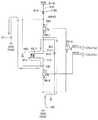
本第3の実施形態に係る磁界発生装置50Cは、基本的に、第2の実施形態のように交番磁界の発生機能は持たずに、コイルの一端側および他端側で交互に切り替えるときに発生する回生電流を駆動電源部側に接続したキャパシタC11に充電して、インダクタL11であるコイルCL11に印加される電圧を上げる機能を有する。 The magnetic field generator 50C according to the third embodiment basically has no function of generating an alternating magnetic field as in the second embodiment, and is alternately switched between one end side and the other end side of the coil. The capacitor C11 connected to the drive power supply unit side with the generated regenerative current is charged to increase the voltage applied to the coil CL11 that is the inductor L11.
磁界発生装置50Cは、導通状態または非導通状態となるように駆動制御部40により制御される、一つのスイッチング部53Cを有する。 The magnetic field generator 50C includes one
スイッチング部53Cは、導通状態となるように制御されたときは、インダクタであるコイルCL11の一端T11を駆動電源部51C側の接続ノードND51Cに接続し、他端T12を基準電位部52Cの接地電位GNDに接続する。
スイッチング部53Cは、非導通状態となるように制御されたときは、インダクタであるコイルCL11の一端T11と駆動電源部51C側の接続ノードND51Cを電気的に切り離しに、他端T12と基準電位部52Cの接地電位GNDとを電気的に切り離す。When the
When the
スイッチング部53Cは、インダクタであるコイルCL11の一端T11と駆動電源部51C側の接続ノードND51Cとの間に接続された第1のスイッチング素子としてのpnp型の第1のトランジスタTR11を有する。
スイッチング部53Cは、コイルCL11の他端T12と基準電位部52Cの接地電位GNDとの間に接続された第2のスイッチング素子としてのnpn型の第2のトランジスタTR12を有する。
さらに、スイッチング部53Cは、第1のトランジスタTR11のベースと接地電位GNDとの間に接続された第5のスイッチング素子としてのnpn型の第5のトランジスタTR15を有する。The
The
Further, the
具体的には、第1のトランジスタTR11のエミッタが接続ノードND51Cに接続され、コレクタがコイルCL11の一端T1に接続され、ベースが第5のトランジスタTR15のコレクタに接続されている。
第2のトランジスタTR12のコレクタがコイルCL11の他端T12に接続され、エミッタが基準電位部52Cの接地電位GNDに接続されている。
第5のトランジスタTR15のエミッタが接地電位GNDに接続されている。
そして、第5のトランジスタTR15のベースがドライバDV11を介して駆動制御部40による制御信号CTL11の供給ラインに接続されている。
第2のトランジスタTR12のベースがドライバDV12を介して駆動制御部40による制御信号CTL12の供給ラインに接続されている。
制御信号CTL12およびCTL13は、同相の信号であり、npn型トランジスタである第5のトランジスタTR15と第2のトランジスタTR12をオン(ON)状態とするハイレベル(H)と、オフ(OFF)状態にするローレベル(L)とが交互に切り替えられる信号として供給される。Specifically, the emitter of the first transistor TR11 is connected to the connection node ND51C, the collector is connected to one end T1 of the coil CL11, and the base is connected to the collector of the fifth transistor TR15.
The collector of the second transistor TR12 is connected to the other end T12 of the coil CL11, and the emitter is connected to the ground potential GND of the reference
The emitter of the fifth transistor TR15 is connected to the ground potential GND.
The base of the fifth transistor TR15 is connected to the supply line of the control signal CTL11 by the
The base of the second transistor TR12 is connected to the supply line of the control signal CTL12 by the
The control signals CTL12 and CTL13 are in-phase signals. The control signals CTL12 and CTL13 are in a high level (H) for turning on the fifth transistor TR15 and the second transistor TR12, which are npn transistors, and in an off (OFF) state. The low level (L) to be supplied is supplied as a signal that can be switched alternately.
磁界発生装置50Cは、接続ノードND51Cと基準電位部の接地電位GNDとの間に接続されたキャパシタC11を有する。
さらに、磁界発生装置50Cは、駆動電源部51Cにおいて、接続ノードN51Cから回生電流の流入を阻止する流入阻止部512Cが配置されている。
流入阻止部512Cは、駆動電源電位部511Cと接続ノードND51Cとの間に、駆動電源電位部511Cから接続ノードND51Cに向かって順方向となるように接続された第3のダイオードD13を含む。
すなわち、第3のダイオードD13のアノードが駆動電源電位部511Cに接続され、カソードが接続ノードND51Cに接続されている。The magnetic field generation device 50C includes a capacitor C11 connected between the connection node ND51C and the ground potential GND of the reference potential unit.
Further, in the magnetic field generator 50C, an
The
That is, the anode of the third diode D13 is connected to the drive power supply potential unit 511C, and the cathode is connected to the connection node ND51C.
さらに、磁界発生装置50Cは、基準電位部52Cの接地電位GND側からコイルCL11を介して駆動電源部51に向かう回生電流(逆起電流)がたどる電流経路を形成する回生電流経路形成部55Cを有する。 Furthermore, the magnetic field generation device 50C includes a regenerative current
回生電流経路形成部55Cは、スイッチング部53Cが非導通状態と導通状態が切り替わったとき、たとえば導通状態から非導通状態となったときに、回生電流の経路を、基準電位部52の接地電位GND、インダクタであるコイルCL11の一端T11、コイル(インダクタ)CL11、コイルCL11の他端T12、キャパシタC11(および接続ノードND51C)の順にたどるように形成する。 When the
回生電流経路形成部55Cは、第1のダイオードD11および第2のダイオードD12を含んで構成されている。 The regenerative current
第1のダイオードD11は、コイル(インダクタ)CL11の他端と駆動電源部51C側の接続ノードND51Cとの間に第1のトランジスタ(第1のスイッチング素子)TR11およびコイル(インダクタ)CL11と並列に、コイルCL11の他端から接続ノードND51Cに向かって順方向となるように接続されている。
すなわち、第1のダイオードD11は、アノードがコイルCL11の他端T12(および第2のトランジスタTR12のコレクタ)に接続され、カソードが接続ノードND51C(および第1のトランジスタTR11のエミッタ)に接続されている。The first diode D11 is in parallel with the first transistor (first switching element) TR11 and the coil (inductor) CL11 between the other end of the coil (inductor) CL11 and the connection node ND51C on the drive
That is, the first diode D11 has an anode connected to the other end T12 of the coil CL11 (and the collector of the second transistor TR12), and a cathode connected to the connection node ND51C (and the emitter of the first transistor TR11). Yes.
第2のダイオードD12は、コイル(インダクタ)CL11の一端T11と基準電位部52の接地電位GNDとの間に第2のトランジスタ(第2のスイッチング素子)TR12およびコイルCL11と並列に、基準電位部52Cの接地電位GNDからコイルCL11の一端T11に向かって順方向となるように接続されている。
すなわち、第2のダイオードD12は、アノードが接地電位GND(および第2のトランジスタTR12のエミッタ)に接続され、カソードがコイルCL11の一端T11(および第1のトランジスタTR11のコレクタ)に接続されている。The second diode D12 is connected between the one end T11 of the coil (inductor) CL11 and the ground potential GND of the reference
That is, the second diode D12 has an anode connected to the ground potential GND (and the emitter of the second transistor TR12) and a cathode connected to one end T11 of the coil CL11 (and the collector of the first transistor TR11). .
次に、第3の実施形態に係る磁界発生装置50Cの動作を、図20〜図22に関連付けて説明する。
この磁界発生装置50Cは、正方向駆動のみ行われ、逆方向駆動は行われない。Next, the operation of the magnetic field generator 50C according to the third embodiment will be described with reference to FIGS.
This magnetic field generator 50C is only driven in the forward direction and is not driven in the reverse direction.
まず、正方向動作を行うように制御信号CTL11,CT12が駆動制御部40から供給される。
この場合、図20に示すように、制御信号CTL11とCTL12がハイレベル(H)で供給される。
これに伴い、第2のトランジスタTR12および第5のトランジスタTR15が導通状態(ON状態)となる。
第5のトランジスタTR15がON状態となったことに伴い、第1のトランジスタTR11のベース電位が接地電位GNDに向かって下がり、第1のトランジスタTR11がON状態となる。
すなわち、正方向動作においては、スイッチング部53CがON状態となる。
これにより、図20中に矢印ZDで示すように、駆動電源部51Dの駆動電源電位部511C、第3のダイオードD13、第1のトランジスタTR11、コイルCL11の一端T11、コイルCL11、コイルCL11の他端T12、第2のトランジスタTR12、基準電位部52Cの接地電位GNDの順にたどる駆動経路が形成される。
これに伴い、コイルCL11の一端T11から他端T12へ電流が流れ、コイルCL11から妨害磁界が発生する。
またこのとき、駆動電源部51CによりキャパシタC11が、たとえば電源電圧VCCのレベル、たとえば12V(あるいは20V)に充電される。First, control signals CTL11 and CT12 are supplied from the
In this case, as shown in FIG. 20, the control signals CTL11 and CTL12 are supplied at a high level (H).
Accordingly, the second transistor TR12 and the fifth transistor TR15 are turned on (ON state).
As the fifth transistor TR15 is turned on, the base potential of the first transistor TR11 decreases toward the ground potential GND, and the first transistor TR11 is turned on.
That is, in the forward operation, the
Accordingly, as indicated by an arrow ZD in FIG. 20, the drive power supply potential unit 511C of the drive
Along with this, a current flows from one end T11 of the coil CL11 to the other end T12, and a disturbing magnetic field is generated from the coil CL11.
At this time, the capacitor C11 is charged to the level of the power supply voltage VCC, for example, 12V (or 20V) by the drive
次に、スイッチング部53CがOFF状態となるように制御信号CTL11,CT12が駆動制御部40から供給される。
この場合、図21に示すように、制御信号CTL11とCTL12がローレベル(L)で供給される。
これに伴い、第2のトランジスタTR12、第5のトランジスタTR15、および第1のトランジスタTR11がOFF状態に保持され,スイッチング部53CがON状態からOFF状態に切り替わる。
スイッチング部53CがON状態からOFF状態に切り替わったとき、図21中に矢印ZIで示すように、回生電流(逆起電流)の経路が、基準電位部52の接地電位GND、第2のダイオードD12、コイル(インダクタ)CL11の一端T11、コイル(インダクタ)CL11、コイルCL11の他端T12、第1のダイオードD11、キャパシタC11の順にたどるように形成される。
このとき、駆動電源部51Cの駆動電源電位部511Cへの回生電流の流入は流入阻止部512Cの第3のダイオードD13で阻止される。
この形成された経路をたどって回生電流が流れ、キャパシタC11に流れ込む。この流れ込んだ回生電流によりキャパシタC11は電源電圧VCC、たとえば12V(あるいは20V)より高い電圧、たとえば20V(あるいは30V)となるように充電される。Next, control signals CTL11 and CT12 are supplied from the
In this case, as shown in FIG. 21, the control signals CTL11 and CTL12 are supplied at a low level (L).
Accordingly, the second transistor TR12, the fifth transistor TR15, and the first transistor TR11 are held in the OFF state, and the
When the
At this time, the inflow of the regenerative current to the drive power supply potential unit 511C of the drive
A regenerative current flows along the formed path and flows into the capacitor C11. Due to the regenerative current that has flown in, the capacitor C11 is charged to a voltage higher than the power supply voltage VCC, eg, 12V (or 20V), for example, 20V (or 30V).
これにより、コイルCL11が発生する磁界が弱くなり、コイルCL11の一端T11から他端T12への回生電流の流れが納まる。 Thereby, the magnetic field generated by the coil CL11 is weakened, and the flow of the regenerative current from one end T11 to the other end T12 of the coil CL11 is stopped.
次に、正方向動作を行うように制御信号CTL11,CT12が駆動制御部40から供給される。
この場合、図22に示すように、制御信号CTL11とCTL12がハイレベル(H)で供給される。
これに伴い、第2のトランジスタTR12および第5のトランジスタTR15がON状態となる。
第5のトランジスタTR15がON状態となったことに伴い、第1のトランジスタTR11のベース電位が接地電位GNDに向かって下がり、第1のトランジスタTR11がON状態となる。
すなわち、正方向動作においては、スイッチング部53CがOFF状態からON状態に切り替わる。
そして、図22中に矢印ZD2で示すように、駆動電源部51Cの駆動電源電位部511C並びにキャパシタC11、第1のトランジスタTR11、コイルCL11の一端T11、コイルCL11、コイルCL11の他端T12、第2のトランジスタTR12、基準電位部52Cの接地電位GNDの順にたどる駆動経路が形成される。
これに伴い、コイルCL11の一端T11から他端T12へ電流が流れ、コイルCL11から妨害磁界が発生する。
このとき、コイルCL11に印加される(かかる)電圧が通常の電源電圧VCCより高い20Vや30Vに昇圧されていることから、コイルCL11に流れる電流も通常より大きくなり、妨害磁界の出力が、増大されている(強くなっている)。Next, control signals CTL11 and CT12 are supplied from the
In this case, as shown in FIG. 22, the control signals CTL11 and CTL12 are supplied at a high level (H).
Accordingly, the second transistor TR12 and the fifth transistor TR15 are turned on.
As the fifth transistor TR15 is turned on, the base potential of the first transistor TR11 decreases toward the ground potential GND, and the first transistor TR11 is turned on.
That is, in the forward direction operation, the
Then, as indicated by an arrow ZD2 in FIG. 22, the drive power supply potential unit 511C of the drive
Along with this, a current flows from one end T11 of the coil CL11 to the other end T12, and a disturbing magnetic field is generated from the coil CL11.
At this time, since the voltage applied (applied) to the coil CL11 is boosted to 20V or 30V higher than the normal power supply voltage VCC, the current flowing through the coil CL11 also becomes larger than usual, and the output of the disturbing magnetic field increases. Has been (strengthened).
以上のようにして、正方向駆動のみで、交番磁界を発生させることなく、妨害磁界の出力を増大させることができる。
すなわち、コイルに印加する電圧の供給を、コイルの一端側および他端側で交互に切り替えるときに発生する回生電流を駆動電源部側に接続したキャパシタC1に充電して、インダクタであるコイルCL11に印加される電圧を上げることができ、磁気データの不正取得を確実に防止することができる。
すなわち、不正行為者が、磁気カードの磁気データを読み取るために、フロントパネルの外部側に、カードリーダのカード挿入口に、磁気ヘッド(スキミングヘッド)と磁気読み取り回路を含むいわゆるスキマー60を取り付けていたとしても、妨害磁界の出力をさらに増大させ、磁気データの不正取得を確実に防止することができる。As described above, the output of the disturbing magnetic field can be increased without generating an alternating magnetic field only by driving in the positive direction.
That is, the regenerative current generated when the supply of the voltage applied to the coil is alternately switched between one end side and the other end side of the coil is charged to the capacitor C1 connected to the drive power supply unit side, and the coil CL11, which is an inductor, is charged. The applied voltage can be increased, and unauthorized acquisition of magnetic data can be reliably prevented.
That is, in order to read the magnetic data of the magnetic card, a fraudulent person attaches a so-called
[磁界発生装置の第4の実施形態]
次に、第4の実施形態に係る磁界発生装置について説明する。
図23は、本発明の第4の実施形態に係る磁界発生装置を示す回路図である。[Fourth Embodiment of Magnetic Field Generator]
Next, a magnetic field generator according to a fourth embodiment will be described.
FIG. 23 is a circuit diagram showing a magnetic field generator according to the fourth embodiment of the present invention.
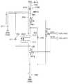
本第4の実施形態に係る磁界発生装置50Dが上述した第3の実施形態に係る磁界発生装置50Cと異なる点は、次の通りである。
本第4の実施形態に係る磁界発生装置50Dは、第1および第2の実施形態の交番磁界の発生機能、並びに第2および第3の実施形態の回線電流の充電機能を備えていない。
ただし、磁界発生装置50Dは、電源電圧VCCを上げれば(たとえば20Vに上げれば)十分に不正行為を阻止可能な回路構成を有する。The
The
However, the magnetic
本第4の実施形態に係る磁界発生装置50Dは、第3の実施形態の磁界発生装置50Cの第1のトランジスタTR11、第5のトランジスタTR15、第2のダイオードD12、第3のダイオードD13(流入阻止部512C)が削除された構成を有している。
すなわち、第4の実施形態に係る磁界発生装置50Dは、基本的な回路を有している。The
That is, the
次に、第4の実施形態に係る磁界発生装置50Dの動作を、図24および図25に関連付けて説明する。
この磁界発生装置50Dは、正方向駆動のみ行われ、逆方向駆動は行われない。Next, the operation of the
This
まず、正方向動作を行うように制御信号CTL12が駆動制御部40から供給される。
この場合、図24に示すように、制御信号CTL12がハイレベル(H)で供給される。
これに伴い、第2のトランジスタTR12が導通状態(ON状態)となる。
すなわち、正方向動作においては、スイッチング部53DがON状態となる。
これにより、図20中に矢印Zで示すように、駆動電源部51Dの駆動電源電位部511D、コイルCL11の一端T11、コイルCL11、コイルCL11の他端T12、第2のトランジスタTR12、基準電位部52Cの接地電位GNDの順にたどる駆動経路が形成される。
これに伴い、コイルCL11の一端T11から他端T12へ電流が流れ、コイルCL11から妨害磁界が発生する。First, the control signal CTL12 is supplied from the
In this case, as shown in FIG. 24, the control signal CTL12 is supplied at a high level (H).
As a result, the second transistor TR12 is turned on (ON state).
That is, in the forward operation, the
Accordingly, as indicated by an arrow Z in FIG. 20, the drive power supply
Along with this, a current flows from one end T11 of the coil CL11 to the other end T12, and a disturbing magnetic field is generated from the coil CL11.
次に、スイッチング部53DがOFF状態となるように制御信号CTL12が駆動制御部40から供給される。
この場合、図25に示すように、制御信号CTL12がローレベル(L)で供給される。
これに伴い、第2のトランジスタTR12がOFF状態となり,スイッチング部53DがON状態からOFF状態に切り替わる。
スイッチング部53DがON状態からOFF状態に切り替わったとき、図25中に矢印ZIで示すように、回生電流(逆起電流)の経路が、駆動電源部51D、コイル(インダクタ)CL11の一端T11、コイル(インダクタ)CL11、コイルCL11の他端T12、第1のダイオードD11、さらには、CL11の一端T11の順にたどるように形成される。
この場合、回生電流はコイルCL11の一端T11から他端T12へ流れ、第1のダイオードD11を介して再度コイルCL11の一端T11から他端T12へ流れ、徐々に減衰していく。
そして、磁界が消滅したころ、再び、図24に関連付けて説明した正方向動作が行われる。Next, the control signal CTL12 is supplied from the
In this case, as shown in FIG. 25, the control signal CTL12 is supplied at a low level (L).
Accordingly, the second transistor TR12 is turned off, and the
When the
In this case, the regenerative current flows from one end T11 of the coil CL11 to the other end T12, and again flows from one end T11 to the other end T12 of the coil CL11 via the first diode D11, and gradually attenuates.
Then, when the magnetic field disappears, the forward direction operation described with reference to FIG. 24 is performed again.
この場合も、不正行為者が、磁気カードの磁気データを読み取るために、フロントパネルの外部側に、カードリーダのカード挿入口に、磁気ヘッド(スキミングヘッド)と磁気読み取り回路を含むいわゆるスキマー60を取り付けていたとしても、妨害磁界を十分に出力することができ、磁気データの不正取得を確実に防止することができる。 Also in this case, in order for an unauthorized person to read the magnetic data of the magnetic card, a so-called
[磁界発生装置の第5の実施形態]
次に、第5の実施形態に係る磁界発生装置について説明する。
図26は、本発明の第5の実施形態に係る磁界発生装置を示す回路図である。[Fifth Embodiment of Magnetic Field Generator]
Next, a magnetic field generator according to a fifth embodiment will be described.
FIG. 26 is a circuit diagram showing a magnetic field generator according to the fifth embodiment of the present invention.
本第5の実施形態に係る磁界発生装置50Eが上述した第1の実施形態に係る図5の磁界発生装置50Aと異なる点は、次の通りである。
磁界発生装置50Eにおいては、図5においてpnp型トランジスタで形成した第1のトランジスタおよび第3のトランジスタを、pチャネルの電界効果トランジスタ(FET)であるPMOSトランジスタTR1P,TR3Pにより形成している。
同様に、磁界発生装置50Eにおいては、図5においてnpn型トランジスタで形成した第2のトランジスタ、第4のトランジスタ、第5のトランジスタ、および第6のトランジスタを、nチャネルのFETであるNMOSトランジスタTR2N,TR4N,TR5N,TR6Nにより形成している。The
In the
Similarly, in the magnetic
その他の構成は、第1の実施形態と同様であり、本第5の実施形態によれば、上述した第1の実施形態と同様の効果を得ることができる。 Other configurations are the same as those of the first embodiment, and according to the fifth embodiment, the same effects as those of the first embodiment described above can be obtained.
[磁界発生装置の第6の実施形態]
次に、第6の実施形態に係る磁界発生装置について説明する。
図27は、本発明の第6の実施形態に係る磁界発生装置を示す回路図である。[Sixth Embodiment of Magnetic Field Generator]
Next, a magnetic field generator according to a sixth embodiment will be described.
FIG. 27 is a circuit diagram showing a magnetic field generator according to the sixth embodiment of the present invention.
本第6の実施形態に係る磁界発生装置50Fが上述した第2の実施形態に係る図12の磁界発生装置50Bと異なる点は、次の通りである。
磁界発生装置50Fにおいては、図12においてpnp型トランジスタで形成した第1のトランジスタおよび第3のトランジスタを、pチャネルのFETであるPMOSトランジスタTR1P,TR3Pにより形成している。
同様に、磁界発生装置50Fにおいては、図12においてnpn型トランジスタで形成した第2のトランジスタ、第4のトランジスタ、第5のトランジスタ、および第6のトランジスタを、nチャネルのFETであるNMOSトランジスタTR2N,TR4N,TR5N,TR6Nにより形成している。The
In the
Similarly, in the magnetic
その他の構成は、第2の実施形態と同様であり、本第6の実施形態によれば、上述した第2の実施形態と同様の効果を得ることができる。 Other configurations are the same as those of the second embodiment, and according to the sixth embodiment, the same effects as those of the second embodiment described above can be obtained.
[磁界発生装置の第7の実施形態]
次に、第7の実施形態に係る磁界発生装置について説明する。
図28は、本発明の第7の実施形態に係る磁界発生装置を示す回路図である。[Seventh Embodiment of Magnetic Field Generator]
Next, a magnetic field generator according to a seventh embodiment will be described.
FIG. 28 is a circuit diagram showing a magnetic field generator according to the seventh embodiment of the present invention.
本第7の実施形態に係る磁界発生装置50Gが上述した第3の実施形態に係る図19の磁界発生装置50Cと異なる点は、次の通りである。
磁界発生装置50Gにおいては、図19においてpnp型トランジスタで形成した第1のトランジスタを、pチャネルのFETであるPMOSトランジスタTR11Pにより形成している。
同様に、磁界発生装置50Gにおいては、図19においてnpn型トランジスタで形成した第2のトランジスタおよび第5のトランジスタを、nチャネルのFETであるNMOSトランジスタTR12N、TR15Nにより形成している。The
In the
Similarly, in the
その他の構成は、第3の実施形態と同様であり、本第7の実施形態によれば、上述した第3の実施形態と同様の効果を得ることができる。 Other configurations are the same as those of the third embodiment, and according to the seventh embodiment, the same effects as those of the third embodiment described above can be obtained.
[磁界発生装置の第7の実施形態]
次に、第8の実施形態に係る磁界発生装置について説明する。
図29は、本発明の第8の実施形態に係る磁界発生装置を示す回路図である。[Seventh Embodiment of Magnetic Field Generator]
Next, a magnetic field generator according to the eighth embodiment will be described.
FIG. 29 is a circuit diagram showing a magnetic field generator according to the eighth embodiment of the present invention.
本第8の実施形態に係る磁界発生装置50Hが上述した第4の実施形態に係る図23の磁界発生装置50Dと異なる点は、次の通りである。
磁界発生装置50Hにおいては、図23においてnpn型トランジスタで形成した第2のトランジスタを、nチャネルのFETであるNMOSトランジスタTR12Nにより形成している。The magnetic field generator 50H according to the eighth embodiment is different from the
In the magnetic field generation device 50H, the second transistor formed by the npn-type transistor in FIG. 23 is formed by the NMOS transistor TR12N which is an n-channel FET.
その他の構成は、第4の実施形態と同様であり、本第8の実施形態によれば、上述した第4の実施形態と同様の効果を得ることができる。 Other configurations are the same as those of the fourth embodiment, and according to the eighth embodiment, the same effects as those of the above-described fourth embodiment can be obtained.
[磁気カードリーダの磁気カード取り込みおよび排出動作]
最後に、一例として、磁気カードリーダ10の磁気カードMCの取り込みおよび排出動作を磁界発生装置50の駆動タイミングと関連付けて説明する。[Magnetic card reader magnetic card loading and unloading]
Finally, as an example, the operation of taking in and ejecting the magnetic card MC of the
まず、取り込み動作を図30および図31に関連付けて説明する。
図30は、磁気カード取込み時の動作を説明するためのフローチャートである。
図31は、磁気カード取込み時の動作を説明するための図である。First, the capturing operation will be described with reference to FIGS.
FIG. 30 is a flowchart for explaining the operation at the time of taking in the magnetic card.
FIG. 31 is a diagram for explaining the operation at the time of taking in the magnetic card.
利用者が磁気カードMCをカードスロット32に挿入すると、挿入された磁気カードMCに形成されている磁気ストライプがカード挿入検出用のプリヘッド33によって検出される(ステップST1)。
このプリヘッド33による検出信号により、駆動制御部40は、妨害磁界発生装置50(50A〜50H)を所定時間駆動して、妨害磁界を発生させる(ステップST2)。
そして、妨害磁界を発生した状態で、駆動制御部40は、駆動モータ38を起動して、取込みローラ対36を含む搬送系を駆動する。同時に、駆動制御部40は、シャッター35を開く(ステップST3)。When the user inserts the magnetic card MC into the
Based on the detection signal from the pre-head 33, the
Then, in the state where the disturbing magnetic field is generated, the
この結果、磁気カードMCを内部に取込み可能になる。
磁気カードMCがシャッター35の位置を超えて奥まで挿入されると、その先端が取込み排出ローラ対36にくわえ込まれて、磁気カードMCの取込み動作が開始される(ステップST4)。As a result, the magnetic card MC can be taken inside.
When the magnetic card MC is inserted beyond the position of the
ここで、本例では、磁気カードMCの取り込みが開始された後は、たとえば磁気カードMCの後端がカードスロット32から突出している状態の間は、妨害磁界発生装置50(50A〜50H)により妨害磁界を発生させ、その後、妨害磁界の発生を停止するようにしている(ステップST5)。
妨害磁界の発生時間は、カード挿入検出用のプリヘッド33による検出時点からの経過時間等によって管理できる。Here, in this example, after the magnetic card MC starts to be taken in, for example, while the rear end of the magnetic card MC protrudes from the
The generation time of the disturbing magnetic field can be managed by the elapsed time from the detection time by the pre-head 33 for detecting card insertion.
次に、磁気カードMCを読み取り用の磁気ヘッド31の位置まで取り込んだ後は、磁気ヘッド31により、磁気カードMCの読み取り動作あるいは書き込み動作を行う(ステップST6)。 Next, after taking the magnetic card MC to the position of the
このように、本例の磁気カードMCの取込み動作においては、磁気カードMCの後端がカードスロット32から突出している時点で、妨害磁界を発生させるようにしている。
この結果、たとえば、図31において想像線で示すように、カードスロット32の外部側位置、たとえば、フロントパネル20の表面に磁気ヘッド(スキミングヘッド)61を含むスキマー60が取り付けられていたとしても、妨害磁界の発生により、挿入される磁気カードMCの磁気データをスキミングヘッド61によっては完全に読み取ることはできない。
よって、このようなスキミングヘッド610による磁気データの不正な読み取りを阻止できる。Thus, in the taking-in operation of the magnetic card MC of this example, the disturbing magnetic field is generated when the rear end of the magnetic card MC protrudes from the
As a result, for example, as shown by an imaginary line in FIG. Due to the generation of the disturbing magnetic field, the magnetic data of the inserted magnetic card MC cannot be read completely by the skimming
Therefore, unauthorized reading of magnetic data by such a skimming head 610 can be prevented.
まず、排出動作を図32および図33に関連付けて説明する。
図32は、磁気カード排出時の動作を説明するためのフローチャートである。
図33は、磁気カード排出時の動作を説明するための図である。First, the discharging operation will be described with reference to FIG. 32 and FIG.
FIG. 32 is a flowchart for explaining the operation when the magnetic card is ejected.
FIG. 33 is a diagram for explaining the operation when the magnetic card is ejected.
この場合、ローラ対36,37−1,37−2によって磁気カードMCの排出動作を開始し(ステップST11)、排出される磁気カードMCの排出方向の後端がフォトセンサ39−1によって検出されると(ステップST12)、妨害磁界発生装置50(50A〜50H)が駆動され、妨害磁界が発生される(ステップST13)。 In this case, the magnetic card MC is ejected by the roller pairs 36, 37-1, and 37-2 (step ST11), and the rear end of the ejected magnetic card MC is detected by the photo sensor 39-1. Then (step ST12), the disturbing magnetic field generator 50 (50A to 50H) is driven to generate a disturbing magnetic field (step ST13).
ここで、図33に示すように、フォトセンサ39−1によって磁気カードMCの後端が検出される状態は、磁気カードMCの排出方向の先端側がカードスロット32から所定の量だけ突き出た状態である。 Here, as shown in FIG. 33, the state in which the rear end of the magnetic card MC is detected by the photosensor 39-1 is a state in which the front end side in the ejection direction of the magnetic card MC protrudes from the
この後は、フォトセンサ39−1よりもカードスロット側に配置されているフォトセンサ39−2によって排出される磁気カードMCの後端が検出されると(ステップST14)、駆動モータ38を停止して(ステップST15)、カード排出動作を終了する。
この後、駆動制御部40は、妨害磁界発生装置50の駆動を止め、妨害磁界の発生を停止させる(ステップST16)。Thereafter, when the rear end of the magnetic card MC ejected by the photo sensor 39-2 arranged on the card slot side with respect to the photo sensor 39-1 is detected (step ST14), the
Thereafter, the
カード排出動作が終了した時点では、磁気カードMCの後端が取込みローラ対36にくわえ込まれた状態にある。
利用者が軽く磁気カードMCを引っ張ることにより、カードスロット32から磁気カードMCを取り出すことができる。
なお、利用者が磁気カードMCを取り出すことを忘れた場合には、所定の時間経過後に、取込みローラ対36を駆動して、磁気カードMCを内部に回収できるようになっている。At the time when the card ejection operation is completed, the rear end of the magnetic card MC is in a state of being inserted into the take-in
When the user pulls the magnetic card MC lightly, the magnetic card MC can be taken out from the
If the user forgets to take out the magnetic card MC, the take-in
このように、本例の磁気カードリーダ10では、磁気カードの排出時においても、その排出側の先端部分がカードスロット32から外部の突き出た状態で、一時的に妨害磁界を発生させるようにしている。
したがって、図2や図3等において示すようなフロントパネル表面にスキミングヘッド61を含むスキマー60が取り付けられていたとしても、このスキミングヘッド61によって排出される磁気カードMCの磁気データが読み取られてしまうことを阻止できる。As described above, in the
Therefore, even if the
なお、本例では、一例であって、妨害磁界発生装置50の駆動を、磁気カード挿入時および排出時に所定の期間にわたり1回だけ駆動しているが、2回以上に渡り間欠的に駆動してもよく、種々の態様が可能である。 In this example, the disturbing
[実施形態の効果]
上述したように、本実施形態においては、以下の効果を得ることができる。
本実施形態に係る磁界発生装置は、インダクタであるコイルに印加する電圧の供給を、コイルの一端側および他端側で交互に切り替えて交番磁界を発生する機能を有する。
この磁界発生装置は、交番磁界を発生するで、妨害磁界の出力を結果的に増大させ、磁気データの不正取得を確実に防止することができる。[Effect of the embodiment]
As described above, the following effects can be obtained in the present embodiment.
The magnetic field generator according to the present embodiment has a function of generating an alternating magnetic field by alternately switching supply of a voltage to be applied to a coil that is an inductor on one end side and the other end side of the coil.
This magnetic field generator generates an alternating magnetic field, thereby increasing the output of the disturbing magnetic field, and reliably preventing unauthorized acquisition of magnetic data.
また、本実施形態に係る磁界発生装置は、交番磁界の発生機能に加えて、コイルに印加する電圧の供給を、コイルの一端側および他端側で交互に切り替えるときに発生する回生電流を駆動電源部側に接続したキャパシタに充電して、インダクタであるコイルに印加される電圧を上げる機能を有する。
したがってこの磁界発生装置は、妨害磁界の出力をさらに増大させることが可能となる。In addition to the function of generating an alternating magnetic field, the magnetic field generator according to the present embodiment drives a regenerative current that is generated when the supply of voltage to be applied to the coil is alternately switched between one end side and the other end side of the coil. The capacitor connected to the power supply side is charged to increase the voltage applied to the inductor coil.
Therefore, this magnetic field generator can further increase the output of the disturbing magnetic field.
さらに、本実施形態に係る磁界発生装置は、交番磁界の発生機能は備えていないが、回生電流を駆動電源部側に接続したキャパシタに充電して、インダクタであるコイルに印加される電圧を上げる機能を有する。
この磁界発生装置においても、妨害磁界の出力を十分に増大させることが可能となる。Furthermore, although the magnetic field generator according to the present embodiment does not have an alternating magnetic field generation function, the regenerative current is charged in a capacitor connected to the drive power supply unit side to increase the voltage applied to the coil that is an inductor. It has a function.
Also in this magnetic field generator, the output of the disturbing magnetic field can be sufficiently increased.
また、本実施形態に係る磁界発生装置は、交番磁界の発生機能、並びに回線電流の充電機能は備えていない場合であっても、電源電圧を上げれば十分に不正行為を阻止可能な回路構成を有する。 In addition, the magnetic field generator according to the present embodiment has a circuit configuration that can sufficiently prevent illegal acts if the power supply voltage is increased, even when the function of generating an alternating magnetic field and the function of charging a line current are not provided. Have.
すなわち、本実施形態に係る磁界発生装置によれば、不正行為者が、磁気カードの磁気データを読み取るために、フロントパネルの外部側に、カードリーダのカード挿入口に、磁気ヘッド(スキミングヘッド)と磁気読み取り回路を含むいわゆるスキマーを取り付けていたとしても、交番磁界を発生することが可能で、妨害磁界の出力を増大させ、磁気データの不正取得を確実に防止することができる。
また、本実施形態では、妨害磁界の発生磁気を、磁気カードの挿入時および排出時としているので、磁気遮蔽板等を設けなくとも、内部の記録・再生用の磁気ヘッドによる動作が阻害されることがない。That is, according to the magnetic field generator according to the present embodiment, a fraudulent person reads the magnetic data of the magnetic card, the magnetic head (skimming head) on the outside of the front panel, the card insertion slot of the card reader. Even if a so-called skimmer including a magnetic reading circuit is attached, it is possible to generate an alternating magnetic field, increase the output of a disturbing magnetic field, and reliably prevent illegal acquisition of magnetic data.
In this embodiment, the magnetic field generated by the disturbing magnetic field is set at the time of insertion and ejection of the magnetic card, so that the operation by the internal recording / reproducing magnetic head is obstructed without providing a magnetic shielding plate or the like. There is nothing.
10・・・磁気カードリーダ(磁気記録媒体理装置)、20・・・フロントパネル。21・・・開口、30・・・磁気カード処理部、31・・・磁気ヘッド、32・・・カードスロット、33・・・プリヘッド、40・・・駆動制御部、50,50A〜50H・・・磁界発生装置、51,51B,51C,51D・・・駆動電源部、511・・・駆動電源電位、512,512C・・・流入阻止部、52,52C・・・基準電位部、53・・・第1のスイッチング部、53C・・・スイッチング部、54・・・第2のスイッチング部、55・・・第1の回生電流経路形成部、55C・・・回生電流経路形成部、56・・・第2の回生電流経路形成部、C1,C11・・・キャパシタ、ND51,ND51B,ND51C・・・接続ノード、MC・・・磁気カード。 10: Magnetic card reader (magnetic recording medium management device), 20: Front panel. DESCRIPTION OF
Claims (10)
Translated fromJapanese駆動電圧を供給する駆動電源部と、
基準電位部と、
前記インダクタの一端を前記駆動電源部に接続し、他端を前記基準電位部に接続する第1のスイッチング部と、
前記インダクタの他端を前記駆動電源部に接続し、一端を前記基準電位部に接続する第2のスイッチング部と、
前記第1のスイッチング部が非導通状態から導通状態となったときに、回生電流の経路を、前記基準電位部、前記インダクタの他端、前記インダクタ、前記インダクタの一端、前記駆動電源部の順にたどるように形成する第1の回生電流経路形成部と、
前記第2のスイッチング部が非導通状態から導通状態となったときに、回生電流の経路を、前記基準電位部、前記インダクタの一端、前記インダクタ、前記インダクタの他端、前記駆動電源部の順にたどるように形成する第2の回生電流経路形成部と、を有し、
前記第1のスイッチング部と前記第2のスイッチング部とが、相補的に導通状態、非導通状態となるように制御される
磁界発生装置。An inductor for generating a magnetic field;
A drive power supply for supplying drive voltage;
A reference potential section;
A first switching unit for connecting one end of the inductor to the drive power supply unit and connecting the other end to the reference potential unit;
A second switching unit that connects the other end of the inductor to the drive power supply unit and connects one end to the reference potential unit;
When the first switching unit is switched from the non-conductive state to the conductive state, the regenerative current path is changed in the order of the reference potential unit, the other end of the inductor, the inductor, one end of the inductor, and the drive power source unit. A first regenerative current path forming unit formed to follow,
When the second switching unit is switched from the non-conductive state to the conductive state, the path of the regenerative current is arranged in the order of the reference potential unit, one end of the inductor, the inductor, the other end of the inductor, and the drive power supply unit. A second regenerative current path forming part formed to follow,
The magnetic field generation device that is controlled so that the first switching unit and the second switching unit are complementarily in a conductive state and a non-conductive state.
前記インダクタの一端と前記駆動電源部との間に接続された第1のスイッチング素子と、
前記インダクタの他端と前記基準電位部との間に接続された第2のスイッチング素子と、を含み、
前記第2のスイッチング部は、
前記インダクタの他端と前記駆動電源部との間に接続された第3のスイッチング素子と、
前記インダクタの一端と前記基準電位部との間に接続された第4のスイッチング素子と、を含む、
請求項1記載の磁界発生装置。The first switching unit includes:
A first switching element connected between one end of the inductor and the drive power supply unit;
A second switching element connected between the other end of the inductor and the reference potential portion,
The second switching unit includes:
A third switching element connected between the other end of the inductor and the drive power supply unit;
A fourth switching element connected between one end of the inductor and the reference potential portion,
The magnetic field generator according to claim 1.
前記インダクタの一端と前記駆動電源部との間に前記第1のスイッチング素子と並列に、当該インダクタの一端から前記駆動電源部に向かって順方向となるように接続された第1のダイオードと、
前記インダクタの他端と前記基準電位部との間に前記第2のスイッチング素子と並列に、基準電位部から当該インダクタの他端に向かって順方向となるように接続された第2のダイオードと、を含み、
前記第2の回生電流経路形成部は、
前記インダクタの他端と前記駆動電源部との間に前記第3のスイッチング素子と並列に、当該インダクタの他端から前記駆動電源部に向かって順方向となるように接続された第3のダイオードと、
前記インダクタの一端と前記基準電位部との間に前記第4のスイッチング素子と並列に、前記基準電位部から当該インダクタの一端に向かって順方向となるように接続された第4のダイオードと、を含む、
請求項2記載の磁界発生装置。The first regenerative current path forming unit includes:
A first diode connected in parallel with the first switching element between one end of the inductor and the drive power supply unit so as to be in a forward direction from one end of the inductor toward the drive power supply unit;
A second diode connected between the other end of the inductor and the reference potential portion in parallel with the second switching element so as to be forward from the reference potential portion toward the other end of the inductor; Including,
The second regenerative current path forming unit includes:
A third diode connected in parallel with the third switching element between the other end of the inductor and the drive power supply unit so as to be in a forward direction from the other end of the inductor toward the drive power supply unit When,
A fourth diode connected in parallel with the fourth switching element between one end of the inductor and the reference potential portion so as to be forward from the reference potential portion toward one end of the inductor; including,
The magnetic field generator according to claim 2.
前記駆動電源部に配置され、前記接続ノードから回生電流の流入を阻止する流入阻止部と、を含む
請求項1から3のいずれか一に記載の磁界発生装置。A connection node to which the drive power supply unit, the first switching unit, the second switching unit, the first regenerative current path forming unit, and the second regenerative current path forming unit are connected, and a reference potential unit; A capacitor connected between
The magnetic field generator according to any one of claims 1 to 3, further comprising: an inflow blocking unit that is disposed in the drive power supply unit and blocks an inflow of a regenerative current from the connection node.
駆動電源電位部と前記接続ノードとの間に、駆動電源電位部から当該接続ノードに向かって順方向となるように接続された第5のダイオードを含む、
請求項4記載の磁界発生装置。The inflow blocking portion is
A fifth diode connected between the drive power supply potential unit and the connection node so as to be in a forward direction from the drive power supply potential unit toward the connection node;
The magnetic field generator according to claim 4.
駆動電圧を接続ノードから供給する駆動電源部と、
基準電位部と、
導通状態と非導通状態が切り替えられ、当該導通状態時に、前記インダクタの一端を前記駆動電源部に接続し、他端を前記基準電位部に接続するスイッチング部と、
前記スイッチング部が導通状態から非導通状態となったときに、回生電流の経路を、前記基準電位部、前記インダクタの一端、前記インダクタ、前記インダクタの他端、前記駆動電源部の接続ノードの順にたどるように形成する回生電流経路形成部と、
前記接続ノードと基準電位部との間に接続されたキャパシタと、
前記駆動電源部に配置され、前記接続ノードから回生電流の流入を阻止する流入阻止部と、
を有する磁界発生装置。An inductor for generating a magnetic field;
A drive power supply for supplying drive voltage from the connection node;
A reference potential section;
A switching unit that switches between a conduction state and a non-conduction state, and connects one end of the inductor to the drive power supply unit and the other end to the reference potential unit during the conduction state;
When the switching unit is switched from the conductive state to the non-conductive state, the regenerative current path is arranged in the order of the reference potential unit, one end of the inductor, the inductor, the other end of the inductor, and a connection node of the drive power supply unit. A regenerative current path forming part that is formed to follow,
A capacitor connected between the connection node and a reference potential unit;
An inflow blocking unit disposed in the drive power supply unit and blocking an inflow of regenerative current from the connection node;
A magnetic field generator.
前記インダクタの一端と駆動電源部との間に接続された第1のスイッチング素子と、
前記インダクタの他端と基準電位部との間に接続された第2のスイッチング素子と、を含む、
請求項6記載の磁界発生装置。The switching unit is
A first switching element connected between one end of the inductor and a drive power supply unit;
A second switching element connected between the other end of the inductor and a reference potential portion,
The magnetic field generator according to claim 6.
前記インダクタの他端と駆動電源部側の前記接続ノードとの間に前記第1のスイッチング素子および前記インダクタと並列に、当該インダクタの他端から前記接続ノードに向かって順方向となるように接続された第1のダイオードと、
前記インダクタの一端と基準電位部との間に前記第2のスイッチング素子および前記インダクタと並列に、基準電位部から当該インダクタの一端に向かって順方向となるように接続された第2のダイオードと、を含む、
請求項7記載の磁界発生装置。The regenerative current path forming unit is
Connected in parallel with the first switching element and the inductor between the other end of the inductor and the connection node on the drive power supply unit side so as to be forward from the other end of the inductor toward the connection node. A first diode formed;
A second diode connected between the one end of the inductor and a reference potential portion in parallel with the second switching element and the inductor so as to be in a forward direction from the reference potential portion toward one end of the inductor; ,including,
The magnetic field generator according to claim 7.
駆動電源電位部と前記接続ノードとの間に、駆動電源電位部から当該接続ノードに向かって順方向となるように接続された第3のダイオードを含む、
請求項6から8のいずれか一に記載の磁界発生装置。The inflow blocking portion is
A third diode connected between the drive power supply potential unit and the connection node so as to be in a forward direction from the drive power supply potential unit toward the connection node;
The magnetic field generator according to any one of claims 6 to 8.
前記内部に挿入された前記磁気記録媒体に対して、磁気データの読み取りおよび書き込のうち少なくとも読み取り行う磁気ヘッドと、
少なくとも前記フロントパネルの外部側に妨害磁界を発生する磁界発生装置と、を有し、
前記磁界発生装置は、
請求項1から9のいずれかに記載された磁界発生装置により構成される
磁気記録媒体処理装置。A front panel in which an opening for inserting or ejecting a magnetic recording medium on which magnetic data is recorded is formed, and partitions the outside and the inside of the magnetic recording medium processing apparatus;
A magnetic head for reading at least one of reading and writing of magnetic data with respect to the magnetic recording medium inserted therein;
A magnetic field generator for generating a disturbing magnetic field at least outside the front panel,
The magnetic field generator is
A magnetic recording medium processing apparatus comprising the magnetic field generator according to claim 1.
Priority Applications (1)
| Application Number | Priority Date | Filing Date | Title |
|---|---|---|---|
| JP2012285651AJP2014128175A (en) | 2012-12-27 | 2012-12-27 | Magnetic field generation device, and magnetic recording medium processing device |
Applications Claiming Priority (1)
| Application Number | Priority Date | Filing Date | Title |
|---|---|---|---|
| JP2012285651AJP2014128175A (en) | 2012-12-27 | 2012-12-27 | Magnetic field generation device, and magnetic recording medium processing device |
Publications (1)
| Publication Number | Publication Date |
|---|---|
| JP2014128175Atrue JP2014128175A (en) | 2014-07-07 |
Family
ID=51407265
Family Applications (1)
| Application Number | Title | Priority Date | Filing Date |
|---|---|---|---|
| JP2012285651APendingJP2014128175A (en) | 2012-12-27 | 2012-12-27 | Magnetic field generation device, and magnetic recording medium processing device |
Country Status (1)
| Country | Link |
|---|---|
| JP (1) | JP2014128175A (en) |
Cited By (1)
| Publication number | Priority date | Publication date | Assignee | Title |
|---|---|---|---|---|
| US10332548B2 (en) | 2017-06-30 | 2019-06-25 | Nidec Sankyo Corporation | Magnetic recording medium processing device and method of generating interference field |
Citations (7)
| Publication number | Priority date | Publication date | Assignee | Title |
|---|---|---|---|---|
| JPS5764910A (en)* | 1980-10-02 | 1982-04-20 | Flowtec Ag | Device for generating predetermined magnetic field of alternative polaritys for measuring magnetic flux dnesity |
| JPS61262038A (en)* | 1985-05-15 | 1986-11-20 | 三菱電機株式会社 | Superconductive coil/energy storage circuit |
| JPS62135205A (en)* | 1985-12-05 | 1987-06-18 | Fuji Electric Co Ltd | Control circuit for electromagnet device |
| JPH02122221A (en)* | 1988-10-31 | 1990-05-09 | Shimadzu Corp | electromagnetic flow meter |
| JPH05268036A (en)* | 1992-03-24 | 1993-10-15 | Aida Eng Ltd | Drive controller for coil load |
| JPH0969435A (en)* | 1995-08-31 | 1997-03-11 | Denso Corp | Inductance load driving bridge circuit |
| JP2001067524A (en)* | 1999-08-31 | 2001-03-16 | Sankyo Seiki Mfg Co Ltd | Magnetic card transaction device |
- 2012
- 2012-12-27JPJP2012285651Apatent/JP2014128175A/enactivePending
Patent Citations (7)
| Publication number | Priority date | Publication date | Assignee | Title |
|---|---|---|---|---|
| JPS5764910A (en)* | 1980-10-02 | 1982-04-20 | Flowtec Ag | Device for generating predetermined magnetic field of alternative polaritys for measuring magnetic flux dnesity |
| JPS61262038A (en)* | 1985-05-15 | 1986-11-20 | 三菱電機株式会社 | Superconductive coil/energy storage circuit |
| JPS62135205A (en)* | 1985-12-05 | 1987-06-18 | Fuji Electric Co Ltd | Control circuit for electromagnet device |
| JPH02122221A (en)* | 1988-10-31 | 1990-05-09 | Shimadzu Corp | electromagnetic flow meter |
| JPH05268036A (en)* | 1992-03-24 | 1993-10-15 | Aida Eng Ltd | Drive controller for coil load |
| JPH0969435A (en)* | 1995-08-31 | 1997-03-11 | Denso Corp | Inductance load driving bridge circuit |
| JP2001067524A (en)* | 1999-08-31 | 2001-03-16 | Sankyo Seiki Mfg Co Ltd | Magnetic card transaction device |
Cited By (1)
| Publication number | Priority date | Publication date | Assignee | Title |
|---|---|---|---|---|
| US10332548B2 (en) | 2017-06-30 | 2019-06-25 | Nidec Sankyo Corporation | Magnetic recording medium processing device and method of generating interference field |
Similar Documents
| Publication | Publication Date | Title |
|---|---|---|
| JP3936496B2 (en) | Magnetic card transaction device | |
| JP6612018B2 (en) | Magnetic field generator, magnetic field generator control method, and magnetic recording medium processing apparatus | |
| US9779273B2 (en) | Magnetic recording medium processing device and control method of the same | |
| CN100576268C (en) | card processing device | |
| JP3693725B2 (en) | Automatic response system using transponder | |
| JP2014128175A (en) | Magnetic field generation device, and magnetic recording medium processing device | |
| JP2015197687A (en) | Magnetic field generator, magnetic recording medium processing device, and control method of the magnetic recording medium processing device | |
| KR950029841A (en) | Camera with magnetic recording head | |
| JP2016189055A (en) | Card reader | |
| US10332548B2 (en) | Magnetic recording medium processing device and method of generating interference field | |
| JP6680931B2 (en) | Magnetic field generator, magnetic field generator control method, and magnetic recording medium processing apparatus | |
| CN113409589B (en) | A detection device and method for occupied charging pile parking space based on microwave perception license plate image | |
| JP5150950B2 (en) | Information recording medium processing apparatus | |
| JP2749525B2 (en) | Card reader | |
| JP2531997B2 (en) | Digital recording circuit | |
| US4769724A (en) | Magnetic head drive apparatus which uses a common current source for the read/write head and the erasing head | |
| CN112065176B (en) | An electric bicycle lock controller with anti-theft function and anti-theft method | |
| JP2008288921A (en) | Remote control system | |
| US20190340395A1 (en) | Card reader device | |
| JPH10341192A (en) | Data transmission circuit | |
| JPS633039Y2 (en) | ||
| EP1906388A1 (en) | Magnetic data erasing device | |
| JPH0419636Y2 (en) | ||
| JPH10221472A5 (en) | ||
| JPS5854611A (en) | Inductive load driving circuit |
Legal Events
| Date | Code | Title | Description |
|---|---|---|---|
| A621 | Written request for application examination | Free format text:JAPANESE INTERMEDIATE CODE: A621 Effective date:20151106 | |
| A131 | Notification of reasons for refusal | Free format text:JAPANESE INTERMEDIATE CODE: A131 Effective date:20160830 | |
| A977 | Report on retrieval | Free format text:JAPANESE INTERMEDIATE CODE: A971007 Effective date:20160830 | |
| A02 | Decision of refusal | Free format text:JAPANESE INTERMEDIATE CODE: A02 Effective date:20170228 |