JP2014123340A - Touch panel - Google Patents
Touch panelDownload PDFInfo
- Publication number
- JP2014123340A JP2014123340AJP2013119753AJP2013119753AJP2014123340AJP 2014123340 AJP2014123340 AJP 2014123340AJP 2013119753 AJP2013119753 AJP 2013119753AJP 2013119753 AJP2013119753 AJP 2013119753AJP 2014123340 AJP2014123340 AJP 2014123340A
- Authority
- JP
- Japan
- Prior art keywords
- touch panel
- bezel
- electrode
- transparent substrate
- set forth
- Prior art date
- Legal status (The legal status is an assumption and is not a legal conclusion. Google has not performed a legal analysis and makes no representation as to the accuracy of the status listed.)
- Pending
Links
Images

Classifications
- G—PHYSICS
- G06—COMPUTING OR CALCULATING; COUNTING
- G06F—ELECTRIC DIGITAL DATA PROCESSING
- G06F3/00—Input arrangements for transferring data to be processed into a form capable of being handled by the computer; Output arrangements for transferring data from processing unit to output unit, e.g. interface arrangements
- G06F3/01—Input arrangements or combined input and output arrangements for interaction between user and computer
- G06F3/03—Arrangements for converting the position or the displacement of a member into a coded form
- G06F3/041—Digitisers, e.g. for touch screens or touch pads, characterised by the transducing means
- G—PHYSICS
- G06—COMPUTING OR CALCULATING; COUNTING
- G06F—ELECTRIC DIGITAL DATA PROCESSING
- G06F2203/00—Indexing scheme relating to G06F3/00 - G06F3/048
- G06F2203/041—Indexing scheme relating to G06F3/041 - G06F3/045
- G06F2203/04103—Manufacturing, i.e. details related to manufacturing processes specially suited for touch sensitive devices
- G—PHYSICS
- G06—COMPUTING OR CALCULATING; COUNTING
- G06F—ELECTRIC DIGITAL DATA PROCESSING
- G06F2203/00—Indexing scheme relating to G06F3/00 - G06F3/048
- G06F2203/041—Indexing scheme relating to G06F3/041 - G06F3/045
- G06F2203/04107—Shielding in digitiser, i.e. guard or shielding arrangements, mostly for capacitive touchscreens, e.g. driven shields, driven grounds
Landscapes
- Engineering & Computer Science (AREA)
- Theoretical Computer Science (AREA)
- General Engineering & Computer Science (AREA)
- Human Computer Interaction (AREA)
- Physics & Mathematics (AREA)
- General Physics & Mathematics (AREA)
- Position Input By Displaying (AREA)
- Computer Hardware Design (AREA)
Abstract
Description
Translated fromJapanese本発明は、タッチパネルに関する。 The present invention relates to a touch panel.
デジタル技術を用いるコンピュータが発達するにつれて、コンピュータの補助装置もともに開発されており、パソコン、携帯用送信装置、その他の個人用の情報処理装置などは、キーボード、マウスなどの様々な入力装置(Input Device)を利用してテキスト及びグラフィック処理を行う。 Along with the development of computers using digital technology, computer auxiliary devices have been developed. Personal computers, portable transmission devices, and other personal information processing devices have various input devices such as keyboards and mice (Inputs). Text and graphics processing is performed using Device).
しかし、情報化社会の急速な進行により、コンピュータの用途が益々拡大する傾向にあるため、現在、入力装置の役割を担当しているキーボード及びマウスだけでは、効率的な製品の駆動が困難であるという問題点がある。従って、簡単で誤操作が少なく、誰でも簡単に情報を入力することができる機器の必要性が高まっている。 However, due to the rapid progress of the information society, the use of computers tends to expand more and more, so it is difficult to drive products efficiently with only the keyboard and mouse that are currently in charge of input devices. There is a problem. Accordingly, there is an increasing need for a device that is simple and has few erroneous operations and that allows anyone to easily input information.
また、入力装置に関する技術は、一般的な機能を満たす水準を越えて、高信頼性、耐久性、革新性、設計及び加工に関する技術などが注目されており、このような目的を達成するために、テキスト、グラフィックなどの情報入力が可能な入力装置として、タッチパネル(Touch Panel)が開発された。 In addition, the technology related to input devices has exceeded the level that satisfies general functions, and attention has been paid to technologies related to high reliability, durability, innovation, design and processing, etc. As an input device that can input information such as text and graphics, a touch panel has been developed.
タッチパネルは、電子手帳、液晶表示装置(LCD;Liquid Crystal Display Device)、PDP(Plasma Display Panel)、El(Electroluminescence)などの平板ディスプレイ装置及びCRT(Cathode Ray Tube)などの画像表示装置の表示面に設けられ、ユーザが画像表示装置を見ながら所望の情報を選択するようにするために利用される機器である。 The touch panel is an image display device such as an electronic notebook, a liquid crystal display device (LCD), a flat panel display device such as a plasma display panel (PDP), an electroluminescence (El), and a display device such as a CRT (Cathode Ray Tube). It is a device that is provided and used for the user to select desired information while looking at the image display device.
タッチパネルの種類は、抵抗膜方式(Resistive Type)、静電容量方式(Capacitive Type)、電磁方式(Electro−Magnetic Type)、表面弾性波方式(SAW Type;Surface Acoustic Wave Type)及び赤外線方式(Infrared Type)に区分される。このような多様な方式のタッチパネルは、信号増幅の問題、解像度の差、設計及び加工技術の難易度、光学的特性、電気的特性、機械的特性、耐環境特性、入力特性、耐久性及び経済性を考慮して電子製品に採用されるが、現在、もっとも幅広い分野で用いられている方式は、抵抗膜方式タッチパネル及び静電容量方式タッチパネルである。 The types of touch panel include a resistive film type, a capacitive type, an electromagnetic type (Electro-Magnetic Type), a surface acoustic wave type (SAW Type; Surface Acoustic Type Infrared type), and an infrared wave type. ). Such various types of touch panels have signal amplification problems, resolution differences, difficulty of design and processing technology, optical characteristics, electrical characteristics, mechanical characteristics, environmental resistance characteristics, input characteristics, durability and economy. However, the most widely used methods in current fields are resistive touch panels and capacitive touch panels.
このようなタッチパネルは、通常、タッチパネル構造の最外側に備えるウィンドウガラス(window glass)に、電極配線を覆ったり、装飾パターンが形成される黒色または白色などの色を有するベゼル部を備える。 Such a touch panel is usually provided with a bezel portion having a color such as black or white on a window glass provided on the outermost side of the touch panel structure so as to cover electrode wiring or to form a decorative pattern.
ベゼル部が形成された従来のタッチパネルの具体的な一例としては、特許文献1に開示されたタッチパネルが挙げられる。 As a specific example of a conventional touch panel in which a bezel portion is formed, a touch panel disclosed in Patent Document 1 can be given.
しかし、従来のタッチパネルは、ベゼル部に電極を形成する際に、ベゼル部の段差によって電極の断線またはクラックが発生するという問題があった。 However, the conventional touch panel has a problem that when the electrode is formed on the bezel portion, the electrode is disconnected or cracked due to the step of the bezel portion.
本発明は、上記の従来技術の問題点を解決するためのものであって、本発明の一目的は、ベゼル部に電極を安定して形成することができるタッチパネルを提供することにある。 The present invention is intended to solve the above-described problems of the prior art, and an object of the present invention is to provide a touch panel capable of stably forming electrodes on a bezel portion.
本発明の一実施例によるベゼル組成物を含むタッチパネルは、活性領域と前記活性領域の縁領域である非活性領域とに区画される透明基板と、前記透明基板の一面に形成される電極と、前記透明基板の一面の前記非活性領域に形成されるベゼルと、を含み、前記ベゼルは、シラン(silane)及び顔料を含むベゼル組成物からなるものである。 A touch panel including a bezel composition according to an embodiment of the present invention includes a transparent substrate partitioned into an active region and a non-active region that is an edge region of the active region, an electrode formed on one surface of the transparent substrate, A bezel formed on the non-active region on one surface of the transparent substrate, and the bezel is made of a bezel composition containing silane and a pigment.
また、本発明の一実施例によるタッチパネルにおいて、前記ベゼルは、側端部に傾斜して形成された傾斜部を含むことができる。 In addition, in the touch panel according to the embodiment of the present invention, the bezel may include an inclined portion formed to be inclined at a side end portion.
また、本発明の一実施例によるタッチパネルにおいて、前記傾斜部は、前記活性領域の方向に向かって高さが次第に低くなるように傾斜して形成されることができる。 In addition, in the touch panel according to an embodiment of the present invention, the inclined portion may be formed to be inclined such that the height gradually decreases in the direction of the active region.
また、本発明の一実施例によるタッチパネルにおいて、前記透明基板の一面と前記傾斜部の傾斜面との間の角度は、10〜80゜に形成されることができる。 In addition, in the touch panel according to an embodiment of the present invention, an angle between one surface of the transparent substrate and the inclined surface of the inclined portion may be 10 to 80 degrees.
また、本発明の一実施例によるタッチパネルにおいて、前記電極は、前記透明基板の前記活性領域及び前記非活性領域に渡って形成されるとともに、前記ベゼルの一面に沿って形成されることができる。 In addition, in the touch panel according to an embodiment of the present invention, the electrode may be formed over the active region and the non-active region of the transparent substrate and along one surface of the bezel.
また、本発明の一実施例によるタッチパネルにおいて、前記電極は、前記透明基板の前記活性領域に形成されるタッチ電極と、前記透明基板の前記非活性領域に形成される電極配線と、を含み、前記電極配線は前記ベゼルの一面に沿って形成されることができる。 In the touch panel according to an embodiment of the present invention, the electrode includes a touch electrode formed in the active region of the transparent substrate, and an electrode wiring formed in the inactive region of the transparent substrate, The electrode wiring may be formed along one surface of the bezel.
また、本発明の一実施例によるタッチパネルにおいて、絶縁物質からなり、前記ベゼルと前記電極との間に形成される遮蔽層をさらに含むことができる。 The touch panel according to an embodiment of the present invention may further include a shielding layer made of an insulating material and formed between the bezel and the electrode.
また、本発明の一実施例によるタッチパネルにおいて、前記ベゼル組成物は、顔料分散剤をさらに含んでなることができる。 In the touch panel according to an embodiment of the present invention, the bezel composition may further include a pigment dispersant.
また、本発明の一実施例によるタッチパネルにおいて、前記ベゼル組成物は、バインダー樹脂をさらに含んでなることができる。 In the touch panel according to the embodiment of the present invention, the bezel composition may further include a binder resin.
また、本発明の一実施例によるタッチパネルにおいて、前記ベゼル組成物は、溶剤をさらに含んでなることができる。 In the touch panel according to an embodiment of the present invention, the bezel composition may further include a solvent.
また、本発明の一実施例によるタッチパネルにおいて、前記ベゼル組成物は、光重合性化合物及び光開始剤をさらに含んでなることができる。 In the touch panel according to an embodiment of the present invention, the bezel composition may further include a photopolymerizable compound and a photoinitiator.
また、本発明の一実施例によるタッチパネルにおいて、前記ベゼル組成物は、高分子化合物、硬化剤、界面活性剤、密着促進剤、酸化防止剤、紫外線吸収剤、凝集防止剤のうち何れか一つ以上を含んでなる添加剤をさらに含むことができる。 In the touch panel according to an embodiment of the present invention, the bezel composition may be any one of a polymer compound, a curing agent, a surfactant, an adhesion promoter, an antioxidant, an ultraviolet absorber, and an aggregation inhibitor. An additive comprising the above can be further included.
また、本発明の一実施例によるタッチパネルにおいて、前記顔料は、二酸化チタン(TiO2)またはカーボンブラック(carbon black)を含んでなることができる。In the touch panel according to an embodiment of the present invention, the pigment may include titanium dioxide (TiO2 ) or carbon black.
本発明によると、ベゼルに傾斜部を形成することにより、段差無く電極を安定して形成することができるため、電極の断線またはクラックの発生を防止することができる。 According to the present invention, since the inclined portion is formed on the bezel, the electrode can be stably formed without a step, and therefore it is possible to prevent the electrode from being disconnected or cracked.
本発明の目的、特定の長所及び新規の特徴は、添付図面に係る以下の詳細な説明及び好ましい実施例によってさらに明らかになるであろう。本明細書において、各図面の構成要素に参照番号を付け加えるに際し、同一の構成要素に限っては、たとえ異なる図面に示されても、できるだけ同一の番号を付けるようにしていることに留意しなければならない。また、「一面」、「他面」、「第1」、「第2」などの用語は、一つの構成要素を他の構成要素から区別するために用いられるものであり、構成要素が前記用語によって限定されるものではない。以下、本発明を説明するにあたり、本発明の要旨を不明瞭にする可能性がある係る公知技術についての詳細な説明は省略する。 Objects, specific advantages and novel features of the present invention will become more apparent from the following detailed description and preferred embodiments with reference to the accompanying drawings. In this specification, it should be noted that when adding reference numerals to the components of each drawing, the same components are given the same number as much as possible even if they are shown in different drawings. I must. The terms “one side”, “other side”, “first”, “second” and the like are used to distinguish one component from another component, and the component is the term It is not limited by. Hereinafter, in describing the present invention, detailed descriptions of known techniques that may obscure the subject matter of the present invention are omitted.
以下、添付図面を参照して、本発明の好ましい実施例を詳細に説明する。
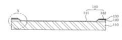
図1は、本発明の一実施例によるタッチパネルにおける透明基板を示した平面図であり、図2は、本発明の一実施例によるタッチパネルを示した断面図であり、図3は、図2に図示されたA領域を拡大して示した断面図である。Hereinafter, preferred embodiments of the present invention will be described in detail with reference to the accompanying drawings.
FIG. 1 is a plan view illustrating a transparent substrate in a touch panel according to an embodiment of the present invention, FIG. 2 is a cross-sectional view illustrating a touch panel according to an embodiment of the present invention, and FIG. It is sectional drawing which expanded and showed A area | region shown in figure.
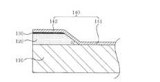
図1から図3に図示されたように、本発明の一実施例によるベゼル組成物を含むタッチパネルは、活性領域111と前記活性領域111の縁領域である非活性領域112とに区画される透明基板110と、前記透明基板110の一面の前記非活性領域112に形成されるベゼル組成物からなるベゼル120と、を含む。 As shown in FIGS. 1 to 3, the touch panel including the bezel composition according to an embodiment of the present invention is divided into an
より詳細には、透明基板110は、タッチ位置を検出するための電極140が形成される領域を提供する役割を遂行することができる。透明基板110は、このような電極140を支持することができる支持力と、画像表示装置から提供される画像をユーザが認識できるようにする透明性を備えなければならない。 In more detail, the
上述の支持力及び透明性を考慮して、透明基板110は、ポリエチレンテレフタレート(PET)、ポリカーボネート(PC)、ポリメチルメタクリレート(PMMA)、ポリエチレンナフタレート(PEN)、ポリエーテルスルフォン(PES)、環状オレフィンコポリマー(COC)、トリアセチルセルロース(Triacetylcellulose;TAC)フィルム、ポリビニルアルコール(Polyvinyl alcohol;PVA)フィルム、ポリイミド(Polyimide;PI)フィルム、ポリスチレン(Polystyrene;PS)、二軸延伸ポリスチレン(K樹脂含有biaxially oriented PS;BOPS)、ガラスまたは強化ガラスなどで形成することが好ましいが、必ずしもこれに限定されるものではない。 In consideration of the above-mentioned supporting force and transparency, the
一方、透明基板110は、図1に図示されたように、活性領域111とこの活性領域111の縁領域である非活性領域112とに区画されることができる。活性領域111は、ユーザによるタッチ作用がなされる領域であり、ユーザが機器の動作場面を視覚的に確認するための画面領域である。また、非活性領域112は、透明基板110に形成される後述するベゼル120によって覆われ、外部に露出されない領域である。 Meanwhile, as shown in FIG. 1, the
ベゼル120は、透明基板110の一面の非活性領域112に形成される(図1参照)。また、ベゼル120は、透明基板110の非活性領域112に対応する領域に配置される電極140の一側を覆う役割を遂行することができる。また、ベゼル120には、必要に応じて、製造社のロゴなどの装飾パターンを形成することもできる。 The
また、ベゼル120は、側端部に傾斜して形成された傾斜部を含む。ここで、傾斜部は、透明基板110の活性領域111の方向に向かって高さが次第に低くなるように傾斜して形成される。この際、透明基板110の一面とベゼル120の傾斜面との間の角度aは、90゜以下である。より詳細には、透明基板110の一面とベゼル120の傾斜面との間の角度aは、10〜80゜であることができる。 Further, the
また、ベゼル120は、シラン(silane)、着色剤及びバインダー樹脂を含むベゼル組成物からなることができる。尚、ベゼル組成物は、光重合性化合物、光重合開始剤、溶剤、添加剤をさらに含むことができる。 Further, the
シランは、ベゼル組成物に含まれて、ベゼル120の傾斜部が形成されるように粘着性を有する。ここで、シランは、RSi(OCNH2NH)3からなることができ、例えば、ビニルトリエトキシシラン(Vinyltriethoxysilane)からなることができる。Silane is included in the bezel composition and has an adhesive property so that an inclined portion of the
着色剤は、顔料及び顔料分散剤を含む着色剤組成物からなることができる。 The colorant can comprise a colorant composition that includes a pigment and a pigment dispersant.
ここで、顔料は、二酸化チタン(TiO2)またはカーボンブラック(carbon black)を含んでなることができるが、本発明の顔料の種類がこれに限定されるものではない。二酸化チタンは、白色顔料であって、着色剤組成物中の固形分に対して質量分率で、50〜90質量%であることができる。この際、二酸化チタンは、例えば、65〜85質量%で着色剤組成物に含まれることができる。Here, the pigment may include titanium dioxide (TiO2 ) or carbon black, but the type of the pigment of the present invention is not limited thereto. Titanium dioxide is a white pigment, and can be 50 to 90% by mass with respect to the solid content in the colorant composition. In this case, titanium dioxide can be included in the colorant composition at 65 to 85% by mass, for example.
また、顔料分散剤は、例えば、ポリエステル系重合体分散剤、アクリル系重合体分散剤、リン酸エステル系分散剤、ポリウレタン系重合体分散剤、カチオン系界面活性剤、アニオン系界面活性剤、ノニオン系界面活性剤のうち何れか一つまたは何れか一つ以上の組合せからなることができる。顔料分散剤の含量は、顔料及び/または染料100重量部に対して1〜10重量部で含まれる。顔料分散剤の含量が前記範囲を満たす場合、均一な分散状態の顔料が得られるため好ましい。 Examples of the pigment dispersant include a polyester polymer dispersant, an acrylic polymer dispersant, a phosphate ester dispersant, a polyurethane polymer dispersant, a cationic surfactant, an anionic surfactant, and a nonion. Any one or a combination of any one or more of the surfactants may be used. The content of the pigment dispersant is 1 to 10 parts by weight with respect to 100 parts by weight of the pigment and / or dye. When the content of the pigment dispersant satisfies the above range, it is preferable because a pigment in a uniform dispersion state can be obtained.
バインダー樹脂は、ゼラチン、ポリビニルアルコール(PVA)、ポリビニルピロリドン(PVP)、澱粉などの多糖類、セルロース及びその誘導体、ポリエチレンオキサイド、ポリビニルアミン、キトサン、ポリリシン、ポリアクリル酸、ポリアルギン酸、ポリヒアルロン酸、カルボキシセルロースのうち何れか一つ以上からなることができる。 Binder resins include gelatin, polyvinyl alcohol (PVA), polyvinyl pyrrolidone (PVP), polysaccharides such as starch, cellulose and its derivatives, polyethylene oxide, polyvinylamine, chitosan, polylysine, polyacrylic acid, polyalginic acid, polyhyaluronic acid, It can consist of any one or more of carboxycellulose.
光重合性化合物は、光及び光重合開始剤の作用により重合されることができる化合物であって、単官能単量体、2官能単量体、その他の多官能単量体のうち何れか一つ以上からなることができる。 The photopolymerizable compound is a compound that can be polymerized by the action of light and a photopolymerization initiator, and is any one of a monofunctional monomer, a bifunctional monomer, and other polyfunctional monomers. Can consist of more than one.
光重合開始剤は、トリアジン系化合物、アセトフェノン系化合物、ビイミダゾール系化合物及びオキシム化合物のうち何れか一つ以上からなることができる。 The photopolymerization initiator can be composed of any one or more of a triazine compound, an acetophenone compound, a biimidazole compound, and an oxime compound.
溶剤としては、エーテル類、芳香族炭化水素類、ケトン類、アルコール類、エステル類またはアミド類などを用いることができる。 As the solvent, ethers, aromatic hydrocarbons, ketones, alcohols, esters or amides can be used.
添加剤は、高分子化合物、硬化剤、界面活性剤、密着促進剤、酸化防止剤、紫外線吸収剤、凝集防止剤などからなることができる。 The additive can be composed of a polymer compound, a curing agent, a surfactant, an adhesion promoter, an antioxidant, an ultraviolet absorber, an aggregation inhibitor, and the like.
電極140は、透明基板110の一面に形成されるとともに、透明基板110の活性領域及び非活性領域に渡って形成されることができる。この際、電極140は、ベゼル120の一面に沿って形成されることができる。ここで、ベゼル120の一面は、図2及び図3において、ベゼル120の上側面であることができる。 The
また、電極140は、透明基板110の前記活性領域に形成されるタッチ電極141と、前記透明基板110の前記非活性領域に形成される電極配線142と、を含む。この際、電極配線142は、ベゼル120の一面に形成することができる。ここで、電極配線142は、タッチ電極141の縁領域に形成され、タッチ電極141からの電気的信号を受信する。 The
具体的には、電極140は、銅(Cu)、アルミニウム(Al)、金(Au)、銀(Ag)、チタン(Ti)、パラジウム(Pd)、クロム(Cr)またはこれらの組合せを用いて、メッシュパターン(Mesh Pattern)に形成することができる。この際、電極140は、メッキ工程または蒸着工程により形成することができる。 Specifically, the
一方、電極140を銅(Cu)で形成する場合、電極140の表面は、黒化処理されることが好ましい。ここで、黒化処理とは、電極140の表面を酸化させてCu2OまたはCuOを析出させることであり、Cu2Oは、茶色を呈するためブラウンオキサイド(Blown Oxide)といい、CuOは、黒色を呈するためブラックオキサイド(Black Oxide)という。このように、電極140の表面を黒化処理することにより、光が反射することを防止することができ、それによって、タッチパネルの視認性を改善させることができる。On the other hand, when the
また、電極140は、線幅が7μm以下に形成され、ピッチが900μm以下に形成されることにより、視認性を改善することができる。しかし、本発明の第1実施例による電極140の線幅及びピッチがこれに限定されるものではない。 Further, the
一方、上述の金属の他にも、電極140は、銀塩乳剤層を露光/現像して形成された金属銀で形成することができる。 On the other hand, in addition to the metal described above, the
また、電極140は、伝導性高分子または金属酸化物を用いて面状に形成することができる。 The
ここで、導電性高分子は、柔軟性に優れており、コーティング工程が単純である。この際、導電性高分子は、ポリ−3,4−エチレンジオキシチオフェン/ポリスチレンスルホネート(PEDOT/PSS)、ポリアニリン、ポリアセチレンまたはポリフェニレンビニレンを含んでなることができる。 Here, the conductive polymer is excellent in flexibility and the coating process is simple. In this case, the conductive polymer may include poly-3,4-ethylenedioxythiophene / polystyrene sulfonate (PEDOT / PSS), polyaniline, polyacetylene, or polyphenylene vinylene.
また、金属酸化物は、インジウム−スズ酸化物(Indium Tin Oxide)からなることができる。 The metal oxide may be made of indium tin oxide.
尚、電極140は、導電性高分子または金属酸化物からなる場合、乾式工程、湿式工程またはダイレクト(direct)パターニング工程により形成することができる。ここで、乾式工程は、スパッタリング(Sputtering)、蒸着(Evaporation)などを意味し、湿式工程は、ディップコーティング(Dip coating)、スピンコーティング(Spin coating)、ロールコーティング(Roll coating)、スプレーコーティング(Spray coating)などを意味し、ダイレクトパターニング工程は、スクリーン印刷法(Screen Printing)、グラビア印刷法(Gravure Printing)、インクジェット印刷法(Inkjet Printing)などを意味する。 The
ここで、電極140は、導電性高分子または金属酸化物からなる場合、図面のように棒形のパターンに形成することができるが、これに限定されず、電極140は、菱形パターン、四角形パターン、三角形パターン、円形パターンなど当業界に公知された全てのパターンに形成することができる。 Here, when the
一方、本発明の一実施例によるタッチパネルは、ベゼル120と電極140との間に形成される遮蔽層130をさらに含むことができる。ここで、遮蔽層130は、絶縁物質からなって、ベゼル120と電極140との間の通電を防止することができる。 Meanwhile, the touch panel according to an embodiment of the present invention may further include a
以上、本発明を具体的な実施例に基づいて詳細に説明したが、これは本発明を具体的に説明するためのものであり、本発明はこれに限定されず、該当分野における通常の知識を有する者であれば、本発明の技術的思想内にての変形や改良が可能であることは明白であろう。 As described above, the present invention has been described in detail based on the specific embodiments. However, the present invention is only for explaining the present invention, and the present invention is not limited thereto. It will be apparent to those skilled in the art that modifications and improvements within the technical idea of the present invention are possible.
本発明の単純な変形乃至変更はいずれも本発明の領域に属するものであり、本発明の具体的な保護範囲は添付の特許請求の範囲により明確になるであろう。 All simple variations and modifications of the present invention belong to the scope of the present invention, and the specific scope of protection of the present invention will be apparent from the appended claims.
本発明は、タッチパネルに適用可能である。 The present invention is applicable to a touch panel.
110 透明基板
111 活性領域
112 非活性領域
120 ベゼル
130 遮蔽層
140 電極
141 タッチ電極
142 電極配線DESCRIPTION OF
Claims (13)
Translated fromJapanese前記透明基板の一面に形成される電極と、
前記透明基板の一面の前記非活性領域に形成されるベゼルと、を含み、
前記ベゼルは、シラン(silane)及び顔料を含むベゼル組成物からなるタッチパネル。A transparent substrate partitioned into an active region and a non-active region that is an edge region of the active region;
An electrode formed on one surface of the transparent substrate;
A bezel formed in the inactive region on one side of the transparent substrate,
The bezel is a touch panel made of a bezel composition including silane and a pigment.
前記透明基板の前記活性領域に形成されるタッチ電極と、
前記透明基板の前記非活性領域に形成される電極配線と、を含み、
前記電極配線は前記ベゼルの一面に沿って形成される請求項1に記載のタッチパネル。The electrode is
A touch electrode formed in the active region of the transparent substrate;
An electrode wiring formed in the inactive region of the transparent substrate,
The touch panel as set forth in claim 1, wherein the electrode wiring is formed along one surface of the bezel.
Applications Claiming Priority (2)
| Application Number | Priority Date | Filing Date | Title |
|---|---|---|---|
| KR1020120150925AKR20140081315A (en) | 2012-12-21 | 2012-12-21 | Touch panel |
| KR10-2012-0150925 | 2012-12-21 |
Publications (1)
| Publication Number | Publication Date |
|---|---|
| JP2014123340Atrue JP2014123340A (en) | 2014-07-03 |
Family
ID=50974236
Family Applications (1)
| Application Number | Title | Priority Date | Filing Date |
|---|---|---|---|
| JP2013119753APendingJP2014123340A (en) | 2012-12-21 | 2013-06-06 | Touch panel |
Country Status (3)
| Country | Link |
|---|---|
| US (1) | US20140176823A1 (en) |
| JP (1) | JP2014123340A (en) |
| KR (1) | KR20140081315A (en) |
Cited By (3)
| Publication number | Priority date | Publication date | Assignee | Title |
|---|---|---|---|---|
| WO2015012228A1 (en)* | 2013-07-25 | 2015-01-29 | 東レ株式会社 | Negative-type photosensitive white composition for touch panel, touch panel, and production method for touch panel |
| JP6081032B1 (en)* | 2015-12-01 | 2017-02-15 | 三菱電機株式会社 | Display device |
| JP2018505915A (en)* | 2014-12-11 | 2018-03-01 | エルジー・ケム・リミテッド | Photosensitive colored ink composition for bezel, bezel pattern formed using the same, and display substrate including the same |
Families Citing this family (5)
| Publication number | Priority date | Publication date | Assignee | Title |
|---|---|---|---|---|
| US9769922B2 (en)* | 2012-02-15 | 2017-09-19 | Heung Sang Yu | White color coating layer-formed touch screen panel and white color coating layer vacuum coating method of touch screen panel |
| KR20140084788A (en)* | 2012-12-27 | 2014-07-07 | 삼성전기주식회사 | Touch Panel And Method For Manufacturing The Same |
| KR102119818B1 (en)* | 2013-09-24 | 2020-06-05 | 엘지이노텍 주식회사 | Touch panel |
| KR102351665B1 (en)* | 2015-01-14 | 2022-01-14 | 삼성디스플레이 주식회사 | Flexible display device |
| US11650705B2 (en)* | 2020-12-07 | 2023-05-16 | Tpk Advanced Solutions Inc. | Touch panel, electronic device and manufacture method thereof |
Family Cites Families (12)
| Publication number | Priority date | Publication date | Assignee | Title |
|---|---|---|---|---|
| WO2004074391A1 (en)* | 1998-05-08 | 2004-09-02 | Takafumi Iida | Ultraviolet-curable adhesive for optical-disk bonding |
| JPH11338637A (en)* | 1998-05-25 | 1999-12-10 | Carol Touch Japan | Optical touch panel |
| US7255451B2 (en)* | 2002-09-20 | 2007-08-14 | Donnelly Corporation | Electro-optic mirror cell |
| DE102005018246A1 (en)* | 2005-04-19 | 2006-10-26 | Schott Ag | Glass or glass ceramic articles with decorative coating |
| DE102008041278A1 (en)* | 2008-08-15 | 2010-02-18 | Evonik Degussa Gmbh | Use of polyolefins as adhesion promoters for the production of laminates |
| KR20110004233A (en)* | 2009-07-07 | 2011-01-13 | (주)삼원에스티 | Touch screen pad and manufacturing method for personal mobile device |
| TWI511019B (en)* | 2009-11-17 | 2015-12-01 | Wistron Corp | Flat-surface resistive touch panel |
| JP5609324B2 (en)* | 2010-06-30 | 2014-10-22 | 大日本印刷株式会社 | Decorative sheet manufacturing method, decorative sheet and decorative molded product using the same |
| KR101699530B1 (en)* | 2010-07-27 | 2017-01-25 | 삼성디스플레이 주식회사 | Touch Screen Panel and Display Device Having the Same |
| US20120295121A1 (en)* | 2011-05-20 | 2012-11-22 | S.T. Trading Company Limited | Fabrication of mirror-like coatings |
| TWI452498B (en)* | 2011-11-02 | 2014-09-11 | Innolux Corp | System for displaying images and fabricating method for touch sensing device |
| KR101861737B1 (en)* | 2011-11-17 | 2018-05-29 | 삼성디스플레이 주식회사 | Optical unit and display device having the same |
- 2012
- 2012-12-21KRKR1020120150925Apatent/KR20140081315A/ennot_activeWithdrawn
- 2013
- 2013-06-06JPJP2013119753Apatent/JP2014123340A/enactivePending
- 2013-06-06USUS13/911,992patent/US20140176823A1/ennot_activeAbandoned
Cited By (5)
| Publication number | Priority date | Publication date | Assignee | Title |
|---|---|---|---|---|
| WO2015012228A1 (en)* | 2013-07-25 | 2015-01-29 | 東レ株式会社 | Negative-type photosensitive white composition for touch panel, touch panel, and production method for touch panel |
| US9690197B2 (en) | 2013-07-25 | 2017-06-27 | Toray Industries, Inc. | Negative-type photosensitive white composition for touch panel, touch panel and touch panel production method |
| JP2018505915A (en)* | 2014-12-11 | 2018-03-01 | エルジー・ケム・リミテッド | Photosensitive colored ink composition for bezel, bezel pattern formed using the same, and display substrate including the same |
| US10739677B2 (en) | 2014-12-11 | 2020-08-11 | Lg Chem, Ltd. | Photosensitive colored ink composition for bezel, bezel pattern formed by using same, and display substrate containing same |
| JP6081032B1 (en)* | 2015-12-01 | 2017-02-15 | 三菱電機株式会社 | Display device |
Also Published As
| Publication number | Publication date |
|---|---|
| US20140176823A1 (en) | 2014-06-26 |
| KR20140081315A (en) | 2014-07-01 |
Similar Documents
| Publication | Publication Date | Title |
|---|---|---|
| JP2014123340A (en) | Touch panel | |
| JP2013137731A (en) | Touch screen | |
| JP5112492B2 (en) | Transparent conductive film for touch panel and manufacturing method thereof | |
| JP2013228986A (en) | Touch panel | |
| US20130169548A1 (en) | Touch panel | |
| JP2013105488A (en) | Touch panel | |
| JP2013254469A (en) | Touch sensor and method of manufacturing the same | |
| JP2013228985A (en) | Touch panel | |
| JP2014021962A (en) | Touch panel and method for manufacturing the same | |
| JP2015153422A (en) | Touch sensor and method of manufacturing the same | |
| JP2013134768A (en) | Sensing electrode pattern for touch panel | |
| JP2012059245A (en) | Touch panel | |
| JP2014063467A (en) | Base plate glass for manufacturing touch panel, and manufacturing method of touch panel using the same | |
| JP2014049114A (en) | Touch panel | |
| KR20120066272A (en) | touch screen | |
| KR20110133359A (en) | Capacitive Touch Panel | |
| JP2014049115A (en) | Touch panel and manufacturing method of the same | |
| JP2015018532A (en) | Touch sensor | |
| JP2014063466A (en) | Touch panel | |
| KR101077424B1 (en) | Touch panel and manufacturing method | |
| JP2014049113A (en) | Touch panel | |
| JP2014120149A (en) | Touch panel | |
| KR20130022570A (en) | Display including touch panel | |
| US20130154966A1 (en) | Touch panel | |
| JP2013134766A (en) | Joint structure for touch panel and method for manufacturing the same |