JP2014110402A - Semiconductor device - Google Patents
Semiconductor deviceDownload PDFInfo
- Publication number
- JP2014110402A JP2014110402AJP2012265615AJP2012265615AJP2014110402AJP 2014110402 AJP2014110402 AJP 2014110402AJP 2012265615 AJP2012265615 AJP 2012265615AJP 2012265615 AJP2012265615 AJP 2012265615AJP 2014110402 AJP2014110402 AJP 2014110402A
- Authority
- JP
- Japan
- Prior art keywords
- film
- gate
- layer
- insulating film
- semiconductor device
- Prior art date
- Legal status (The legal status is an assumption and is not a legal conclusion. Google has not performed a legal analysis and makes no representation as to the accuracy of the status listed.)
- Pending
Links
Images


Classifications
- H—ELECTRICITY
- H10—SEMICONDUCTOR DEVICES; ELECTRIC SOLID-STATE DEVICES NOT OTHERWISE PROVIDED FOR
- H10D—INORGANIC ELECTRIC SEMICONDUCTOR DEVICES
- H10D30/00—Field-effect transistors [FET]
- H10D30/60—Insulated-gate field-effect transistors [IGFET]
- H10D30/64—Double-diffused metal-oxide semiconductor [DMOS] FETs
- H10D30/66—Vertical DMOS [VDMOS] FETs
- H10D30/668—Vertical DMOS [VDMOS] FETs having trench gate electrodes, e.g. UMOS transistors
- H—ELECTRICITY
- H10—SEMICONDUCTOR DEVICES; ELECTRIC SOLID-STATE DEVICES NOT OTHERWISE PROVIDED FOR
- H10D—INORGANIC ELECTRIC SEMICONDUCTOR DEVICES
- H10D62/00—Semiconductor bodies, or regions thereof, of devices having potential barriers
- H10D62/80—Semiconductor bodies, or regions thereof, of devices having potential barriers characterised by the materials
- H10D62/83—Semiconductor bodies, or regions thereof, of devices having potential barriers characterised by the materials being Group IV materials, e.g. B-doped Si or undoped Ge
- H10D62/8303—Diamond
- H—ELECTRICITY
- H10—SEMICONDUCTOR DEVICES; ELECTRIC SOLID-STATE DEVICES NOT OTHERWISE PROVIDED FOR
- H10D—INORGANIC ELECTRIC SEMICONDUCTOR DEVICES
- H10D62/00—Semiconductor bodies, or regions thereof, of devices having potential barriers
- H10D62/80—Semiconductor bodies, or regions thereof, of devices having potential barriers characterised by the materials
- H10D62/83—Semiconductor bodies, or regions thereof, of devices having potential barriers characterised by the materials being Group IV materials, e.g. B-doped Si or undoped Ge
- H10D62/832—Semiconductor bodies, or regions thereof, of devices having potential barriers characterised by the materials being Group IV materials, e.g. B-doped Si or undoped Ge being Group IV materials comprising two or more elements, e.g. SiGe
- H10D62/8325—Silicon carbide
- H—ELECTRICITY
- H10—SEMICONDUCTOR DEVICES; ELECTRIC SOLID-STATE DEVICES NOT OTHERWISE PROVIDED FOR
- H10D—INORGANIC ELECTRIC SEMICONDUCTOR DEVICES
- H10D62/00—Semiconductor bodies, or regions thereof, of devices having potential barriers
- H10D62/80—Semiconductor bodies, or regions thereof, of devices having potential barriers characterised by the materials
- H10D62/85—Semiconductor bodies, or regions thereof, of devices having potential barriers characterised by the materials being Group III-V materials, e.g. GaAs
- H10D62/8503—Nitride Group III-V materials, e.g. AlN or GaN
- H—ELECTRICITY
- H10—SEMICONDUCTOR DEVICES; ELECTRIC SOLID-STATE DEVICES NOT OTHERWISE PROVIDED FOR
- H10D—INORGANIC ELECTRIC SEMICONDUCTOR DEVICES
- H10D64/00—Electrodes of devices having potential barriers
- H10D64/20—Electrodes characterised by their shapes, relative sizes or dispositions
- H10D64/27—Electrodes not carrying the current to be rectified, amplified, oscillated or switched, e.g. gates
- H10D64/311—Gate electrodes for field-effect devices
- H10D64/411—Gate electrodes for field-effect devices for FETs
- H10D64/511—Gate electrodes for field-effect devices for FETs for IGFETs
- H10D64/512—Disposition of the gate electrodes, e.g. buried gates
- H10D64/513—Disposition of the gate electrodes, e.g. buried gates within recesses in the substrate, e.g. trench gates, groove gates or buried gates
- H—ELECTRICITY
- H10—SEMICONDUCTOR DEVICES; ELECTRIC SOLID-STATE DEVICES NOT OTHERWISE PROVIDED FOR
- H10D—INORGANIC ELECTRIC SEMICONDUCTOR DEVICES
- H10D64/00—Electrodes of devices having potential barriers
- H10D64/60—Electrodes characterised by their materials
- H10D64/66—Electrodes having a conductor capacitively coupled to a semiconductor by an insulator, e.g. MIS electrodes
- H10D64/661—Electrodes having a conductor capacitively coupled to a semiconductor by an insulator, e.g. MIS electrodes the conductor comprising a layer of silicon contacting the insulator, e.g. polysilicon having vertical doping variation
- H—ELECTRICITY
- H10—SEMICONDUCTOR DEVICES; ELECTRIC SOLID-STATE DEVICES NOT OTHERWISE PROVIDED FOR
- H10D—INORGANIC ELECTRIC SEMICONDUCTOR DEVICES
- H10D64/00—Electrodes of devices having potential barriers
- H10D64/60—Electrodes characterised by their materials
- H10D64/66—Electrodes having a conductor capacitively coupled to a semiconductor by an insulator, e.g. MIS electrodes
- H10D64/665—Electrodes having a conductor capacitively coupled to a semiconductor by an insulator, e.g. MIS electrodes the conductor comprising a layer of elemental metal contacting the insulator, e.g. tungsten or molybdenum
- H—ELECTRICITY
- H10—SEMICONDUCTOR DEVICES; ELECTRIC SOLID-STATE DEVICES NOT OTHERWISE PROVIDED FOR
- H10D—INORGANIC ELECTRIC SEMICONDUCTOR DEVICES
- H10D64/00—Electrodes of devices having potential barriers
- H10D64/60—Electrodes characterised by their materials
- H10D64/66—Electrodes having a conductor capacitively coupled to a semiconductor by an insulator, e.g. MIS electrodes
- H10D64/68—Electrodes having a conductor capacitively coupled to a semiconductor by an insulator, e.g. MIS electrodes characterised by the insulator, e.g. by the gate insulator
- H10D64/681—Electrodes having a conductor capacitively coupled to a semiconductor by an insulator, e.g. MIS electrodes characterised by the insulator, e.g. by the gate insulator having a compositional variation, e.g. multilayered
- H10D64/685—Electrodes having a conductor capacitively coupled to a semiconductor by an insulator, e.g. MIS electrodes characterised by the insulator, e.g. by the gate insulator having a compositional variation, e.g. multilayered being perpendicular to the channel plane
- H—ELECTRICITY
- H10—SEMICONDUCTOR DEVICES; ELECTRIC SOLID-STATE DEVICES NOT OTHERWISE PROVIDED FOR
- H10D—INORGANIC ELECTRIC SEMICONDUCTOR DEVICES
- H10D64/00—Electrodes of devices having potential barriers
- H10D64/60—Electrodes characterised by their materials
- H10D64/66—Electrodes having a conductor capacitively coupled to a semiconductor by an insulator, e.g. MIS electrodes
- H10D64/68—Electrodes having a conductor capacitively coupled to a semiconductor by an insulator, e.g. MIS electrodes characterised by the insulator, e.g. by the gate insulator
- H10D64/691—Electrodes having a conductor capacitively coupled to a semiconductor by an insulator, e.g. MIS electrodes characterised by the insulator, e.g. by the gate insulator comprising metallic compounds, e.g. metal oxides or metal silicates
- H—ELECTRICITY
- H10—SEMICONDUCTOR DEVICES; ELECTRIC SOLID-STATE DEVICES NOT OTHERWISE PROVIDED FOR
- H10D—INORGANIC ELECTRIC SEMICONDUCTOR DEVICES
- H10D64/00—Electrodes of devices having potential barriers
- H10D64/60—Electrodes characterised by their materials
- H10D64/66—Electrodes having a conductor capacitively coupled to a semiconductor by an insulator, e.g. MIS electrodes
- H10D64/68—Electrodes having a conductor capacitively coupled to a semiconductor by an insulator, e.g. MIS electrodes characterised by the insulator, e.g. by the gate insulator
- H10D64/693—Electrodes having a conductor capacitively coupled to a semiconductor by an insulator, e.g. MIS electrodes characterised by the insulator, e.g. by the gate insulator the insulator comprising nitrogen, e.g. nitrides, oxynitrides or nitrogen-doped materials
- H—ELECTRICITY
- H10—SEMICONDUCTOR DEVICES; ELECTRIC SOLID-STATE DEVICES NOT OTHERWISE PROVIDED FOR
- H10D—INORGANIC ELECTRIC SEMICONDUCTOR DEVICES
- H10D64/00—Electrodes of devices having potential barriers
- H10D64/20—Electrodes characterised by their shapes, relative sizes or dispositions
- H10D64/23—Electrodes carrying the current to be rectified, amplified, oscillated or switched, e.g. sources, drains, anodes or cathodes
- H10D64/251—Source or drain electrodes for field-effect devices
- H10D64/256—Source or drain electrodes for field-effect devices for lateral devices wherein the source or drain electrodes are recessed in semiconductor bodies
Landscapes
- Electrodes Of Semiconductors (AREA)
Abstract
Translated fromJapaneseDescription
Translated fromJapanese本発明は、MIS構造を有する半導体装置に関する。 The present invention relates to a semiconductor device having a MIS structure.
SiC(炭化シリコン:シリコンカーバイト)は、Si(シリコン)よりも絶縁破壊耐性および熱伝導率などに優れている。そのため、SiCは、たとえば、ハイブリッド自動車のインバータなどの用途に好適な半導体として注目されている。SiCを用いたMISFET(Metal Insulator Semiconductor Field Effect Transistor)は、ハイブリッド自動車のインバータなどに好適な高耐圧デバイスとして期待されている。 SiC (silicon carbide: silicon carbide) is superior in dielectric breakdown resistance and thermal conductivity to Si (silicon). Therefore, SiC attracts attention as a semiconductor suitable for applications such as an inverter of a hybrid vehicle. A MISFET (Metal Insulator Semiconductor Field Effect Transistor) using SiC is expected as a high voltage device suitable for an inverter of a hybrid vehicle.
SiCを用いたMISFETの一例として、特許文献1は、n型のSiC基板と、当該SiC基板上に形成されたn型ドリフト層と、ドリフト層に形成されたp型ウェル領域と、p型ウェル領域に形成されたn型ソース領域と、ドリフト層の表面に形成されたゲート絶縁膜と、ゲート絶縁膜上に形成されたゲート電極とを含むSiC半導体装置を開示している。 As an example of a MISFET using SiC,
特許文献1のようなSiC−MISFETの課題の一つとして、低チャネル移動度がある。低チャネル移動度は、SiCのMIS界面に高密度に存在する欠陥(界面準位が多いこと)が原因である。すなわち、この欠陥が、正孔または電子を捕獲(トラップ)し、MIS界面にチャネルを形成し難くする。
従来は、比較的薄いSiO2膜をゲート絶縁膜として使用し、Si−MISFETに比べて高い電界でゲートを駆動することによって、捕獲された正孔または電子が欠陥から解放され易くしていた。しかしながら、このやり方は、ゲート絶縁膜の劣化を加速させ、デバイスの信頼性の低下を招くおそれがある。One of the problems of the SiC-MISFET as in
Conventionally, a relatively thin SiO2 film is used as a gate insulating film, and the trapped holes or electrons are easily released from defects by driving the gate with a higher electric field than Si-MISFET. However, this method accelerates the deterioration of the gate insulating film and may lead to a decrease in device reliability.
これに対し、ゲート絶縁膜としてAl2O3膜やHfO2等の高誘電率膜(High−k膜)を使用すれば、同じゲート容量を維持しながら、SiO2膜に比べて膜厚を大きくできるかもしれない。しかし、この場合には、ゲート絶縁膜中に電子が捕獲されてフラットバンド電圧VFBがシフトし、閾値電圧Vthがシフトするという問題が発生する。
そこで、本発明の目的は、ゲート絶縁膜中への電子トラップを低減し、閾値電圧Vthのシフトを抑制することができる半導体装置を提供することである。On the other hand, if a high dielectric constant film (High-k film) such as an Al2 O3 film or HfO2 is used as the gate insulating film, the film thickness can be increased as compared with the SiO2 film while maintaining the same gate capacitance. May be bigger. However, in this case, there is a problem that electrons are trapped in the gate insulating film, the flat band voltageVFB is shifted, and the threshold voltageVth is shifted.
Accordingly, an object of the present invention is to provide a semiconductor device capable of reducing electron traps in a gate insulating film and suppressing a shift in threshold voltageVth .
本発明は、半導体層と、前記半導体層に接するゲート絶縁膜と、前記ゲート絶縁膜上に形成されたゲート電極とを含むMIS構造を有し、前記ゲート絶縁膜は、窒素組成が5%〜40%のAlON層を含む(請求項1)。
この構成によれば、ゲート絶縁膜が5%〜40%の窒素組成を有するAlON層を含むので、ゲート絶縁膜中への電子トラップを低減することができる。これによりフラットバンド電圧VFBのシフトを抑制することができるので、閾値電圧Vthのシフトを抑制することができる。また、ゲートリーク電流を低減することができる。また、SiO2の単層膜を用いる場合に比べて、同じゲート容量を維持しながら厚くすることができるので、高い電圧でゲートを駆動させてもゲート絶縁膜の劣化を抑制することができる。その結果、デバイスの信頼性の低下を抑制することができる。The present invention has a MIS structure including a semiconductor layer, a gate insulating film in contact with the semiconductor layer, and a gate electrode formed on the gate insulating film, and the gate insulating film has a nitrogen composition of 5% to 40% AlON layer is included (claim 1).
According to this configuration, since the gate insulating film includes the AlON layer having a nitrogen composition of 5% to 40%, electron traps in the gate insulating film can be reduced. Thereby, since the shift of the flat band voltageVFB can be suppressed, the shift of the threshold voltageVth can be suppressed. In addition, gate leakage current can be reduced. In addition, since the thickness can be increased while maintaining the same gate capacity as compared with the case where a single layer film of SiO2 is used, deterioration of the gate insulating film can be suppressed even when the gate is driven at a high voltage. As a result, a decrease in device reliability can be suppressed.
また、前記AlON層は50nm以上の厚さを有することが好ましい(請求項2)。
前記AlON層はアモルファスまたは微結晶であることが好ましい(請求項3)。この構成により、ゲート絶縁膜中の結晶粒界を減らすことができるので、ゲートリーク電流を低減することができる。
前記ゲート絶縁膜は、前記半導体層に接する下地SiO2層と、この下地SiO2層に積層された前記AlON層とを含む積層構造を有することが好ましい(請求項4)。ゲート絶縁膜の半導体層に接する部分がSiO2であれば、フラットバンド電圧VFBのシフト量を低減することができる。また、MIS構造のトランジスタの特性を従来と同じように制御することができので、トランジスタ特性の設計を簡単にすることができる。なお、下地SiO2層は熱酸化膜であることが好ましい。The AlON layer preferably has a thickness of 50 nm or more.
The AlON layer is preferably amorphous or microcrystalline. With this configuration, since the grain boundary in the gate insulating film can be reduced, the gate leakage current can be reduced.
The gate insulating film preferably has a stacked structure including a base SiO2 layer in contact with the semiconductor layer and the AlON layer stacked on the base SiO2 layer. If the portion of the gate insulating film in contact with the semiconductor layer is SiO2 , the shift amount of the flat band voltageVFB can be reduced. In addition, since the characteristics of the MIS structure transistor can be controlled in the same manner as in the past, the design of the transistor characteristics can be simplified. The underlying SiO2 layer is preferably a thermal oxide film.
前記下地SiO2層は5nm以上の厚さを有することが好ましい(請求項5)。この構成により、ゲートリーク電流の立ち上がり電界を高くすることができるので、ゲートの通常駆動時におけるリーク電流の発生を抑制することができる。
前記積層構造は、前記AlON層に積層された上側SiO2層をさらに含むことが好ましい(請求項6)。この構成により、AlON層が上側から覆われるので、たとえばゲート電極形成時に、エッチングや洗浄に用いる薬剤からAlON層を保護することができる。その結果、AlON層がダメージを受けることを抑制することができる。The underlayer SiO2 layer preferably has a thickness of 5 nm or more. With this configuration, the rising electric field of the gate leakage current can be increased, so that the generation of leakage current during normal driving of the gate can be suppressed.
Preferably, the stacked structure further includes an upper SiO2 layer stacked on the AlON layer. With this configuration, since the AlON layer is covered from above, the AlON layer can be protected from chemicals used for etching and cleaning, for example, when forming the gate electrode. As a result, the AlON layer can be prevented from being damaged.
また、前記上側SiO2層は、前記AlON層との界面部にAlおよび/またはNを含有していることが好ましい(請求項7)。この構成により、ゲート絶縁膜への電子注入を抑制することができる。
前記半導体層はSiC、GaNまたはダイヤモンドからなっていてもよい(請求項8)。また、前記ゲート電極は、ポリシリコンもしくは、Mo、W、Cu、Ni、Al、Ti、Ag、AuおよびPtからなる群から選択される少なくとも1種を含有する金属からなることが好ましい(請求項9)。金属電極(金属ゲート)の場合、たとえばポリシリコン電極(ポリシリコンゲート)に比べて低温で成膜することができるので、当該成膜時の温度環境を低めに抑えることができる。これにより、AlON層が結晶化温度に達し難くなるので、AlON層の結晶化を抑えることができる。その結果、結晶粒界の増加によるゲートリーク電流の増加を抑制することができる。また、ポリシリコンゲートに比べてゲート抵抗を低減することができるので、より高速なスイッチング動作を実現でき、スイッチング損失を低減することができる。The upper SiO2 layer preferably contains Al and / or N at the interface with the AlON layer. With this configuration, electron injection into the gate insulating film can be suppressed.
The semiconductor layer may be made of SiC, GaN, or diamond. The gate electrode is preferably made of polysilicon or a metal containing at least one selected from the group consisting of Mo, W, Cu, Ni, Al, Ti, Ag, Au, and Pt. 9). In the case of a metal electrode (metal gate), film formation can be performed at a lower temperature than, for example, a polysilicon electrode (polysilicon gate), so that the temperature environment during the film formation can be kept low. This makes it difficult for the AlON layer to reach the crystallization temperature, so that crystallization of the AlON layer can be suppressed. As a result, an increase in gate leakage current due to an increase in crystal grain boundaries can be suppressed. Further, since the gate resistance can be reduced as compared with the polysilicon gate, a higher-speed switching operation can be realized and the switching loss can be reduced.
また、前記MIS構造は、トレンチゲート型の構造を含んでいてもよいし(請求項10)、プレーナゲート構造を含んでいてもよい(請求項11)。 Further, the MIS structure may include a trench gate type structure (Claim 10), or may include a planar gate structure (Claim 11).
以下では、本発明の実施の形態を、添付図面を参照して詳細に説明する。
図1は、本発明の第1の実施形態に係る半導体装置の断面図である。
半導体装置1は、n+型(たとえば、濃度が1×10¹⁹〜5×1019cm−3)のSiC基板2と、SiC基板2上に形成されたn−型(たとえば、濃度が1×10¹⁵〜1×1016cm−3)のSiCエピタキシャル層3とを含む。SiC基板2およびSiCエピタキシャル層3が、本発明の「半導体層」の一例である。SiC基板2およびSiCエピタキシャル層3は、半導体装置1のドレインとして機能する。n型不純物としては、リン(P)、ヒ素(As)などが含まれている。以下、n型SiCには同様のn型不純物が含まれている。Hereinafter, embodiments of the present invention will be described in detail with reference to the accompanying drawings.
FIG. 1 is a sectional view of a semiconductor device according to the first embodiment of the present invention.
SiCエピタキシャル層3には、その表面からSiC基板2へ向かって掘り下がった、ゲートトレンチ4が形成されている。ゲートトレンチ4は、たとえば、格子状、ストライプ状に形成されている。これにより、SiCエピタキシャル層3には、ゲートトレンチ4により区画された単位セル5が複数形成されている。
SiCエピタキシャル層3においてゲートトレンチ4の周囲には、n+型のソース領域6およびp型(たとえば、濃度が1×10¹⁷〜5×1017cm−3)のボディ領域7が、SiCエピタキシャル層3の表面に近い側からこの順に形成されている。ボディ領域7には、p型不純物として、たとえば、ボロン(B)、アルミニウム(Al)などが含まれている。以下、p型SiCには同様のp型不純物が含まれている。The
Around the
ソース領域6は、SiCエピタキシャル層3の表面に露出するとともに、ゲートトレンチ4の側面の上部(一部)を形成するように、各単位セル5の表面部に形成されている。一方、ボディ領域7は、ソース領域6に対してSiC基板2側(SiCエピタキシャル層3の裏面側)にソース領域6に接するように、かつ、ゲートトレンチ4の側面の下部(一部)を形成するように形成されている。 The
SiCエピタキシャル層3における、ボディ領域7に対してSiC基板2側の領域は、エピタキシャル成長後のままの状態が維持された、n−型のドレイン領域8となっている。ドレイン領域8は、ボディ領域7に対してSiC基板2側にボディ領域7に接しており、ゲートトレンチ4の底面を形成している。
ゲートトレンチ4の内面には、その全域を覆うように、ゲート絶縁膜9が形成されている。ゲート絶縁膜9は、ゲートトレンチ4の内面側から順に積層された下地SiO2膜10、AlON膜11および上側SiO2膜12を含む。この実施形態では、ゲートトレンチ4の内面全域に接するように下地SiO2膜10が形成され、その上に、下地SiO2膜10と同じ形状のAlON膜11および上側SiO2膜12が、それぞれ直下の膜の全域を覆うように順に積層されている。なお、これらの膜の3層構造は、この実施形態のようにゲートトレンチ4の内面全域に亘って形成されていてもよいし、ゲートトレンチ4の内面におけるチャネル部分(ゲートトレンチ4の側面においてボディ領域7が露出する部分)に選択的に形成されていてもよい。この場合、ゲート絶縁膜9の他の部分は、SiO2からなる単層膜であってもよい。また、ゲート絶縁膜9は、AlON膜11の単層膜であってもよいし、上側SiO2膜12が省略された2層構造の膜(下地SiO2膜10/AlON膜11)であってもよい。また、ゲート絶縁膜9は、この実施形態では、ゲートトレンチ4の開口端側エッジ部を覆うように形成されていてもよい。ゲートトレンチ4の開口端側エッジ部は、SiCエピタキシャル層3の表面とゲートトレンチ4の側面との挟角を形成している。したがって、ソース領域6におけるSiCエピタキシャル層3の表面およびゲートトレンチ4の側面の各近傍部分はゲート絶縁膜9に覆われることとなる。In the
A
ゲート絶縁膜9の厚さは、たとえば、55nm〜150nmである。各膜の厚さの好ましい範囲は、下地SiO2膜10が5nm以上(より好ましくは、5nm〜20nm)であり、AlON膜11が50nm以上(より好ましくは、50nm〜100nm)であり、上側SiO2膜12が0nm以上(より好ましくは、0nm〜30nm)である。
下地SiO2膜10は、この実施形態では、たとえばSiCエピタキシャル層3を熱酸化によって形成されている。SiCエピタキシャル層3(特に、チャネル部分)に接する膜を熱酸化膜とすることによって、CVD膜等の堆積膜に比べて優れたトランジスタ特性を発現することができる。The thickness of the
In this embodiment, base SiO2 film 10 is formed, for example, by thermal oxidation of
AlON膜11は、膜中に窒素(N)原子が分散した膜であって、たとえば窒素組成が5%〜40%(好ましくは、15%〜35%)の膜である。当該窒素組成は、AlON膜11の深さ方向いずれの位置においても上記範囲に収まっている。すなわち、AlON膜11の窒素組成は深さ方向にほぼ一定であり、好ましくは、深さ方向の平均値に対して±5%〜±20%以内に収まっている。なお、AlON膜11の他の原子(Al、O)についても、それらの組成が深さ方向にほぼ一定であることが好ましい。窒素組成が上記範囲であれば、半導体装置1のフラットバンド電圧VFBをより良好に抑制できると共に、ゲートリーク電流を低減することができる。また、AlON膜11は、アモルファスまたは微結晶であることが好ましい。AlON膜11がそのような構造であれば、ゲート絶縁膜9中の結晶粒界を減らすことができるので、ゲートリーク電流を低減することができる。The
上側SiO2膜12は、主に酸化シリコンからなるが、AlON膜11との界面部(界面近傍)にAlおよび/またはNを含有していてもよい。この構成により、ゲート絶縁膜9への電子注入を抑制することができる。
このようなゲート絶縁膜9は、たとえば、SiCエピタキシャル層3にゲートトレンチ4を形成した後、下地SiO2膜10、AlON膜11および上側SiO2膜12を順に積層することによって形成することができる。下地SiO2膜10は、たとえば熱酸化法(たとえば、1100℃〜1300℃)によって形成することができる。また、AlON膜11は、たとえばALD(Atomic Layer Deposition:原子層堆積)法、CVD法、PVD(Physical Vapor Deposition:物理気相成長)法等によって各原子を堆積させることによって形成することができる。また、上側SiO2膜12は、たとえばCVD法によって形成することができる。The upper SiO2 film 12 is mainly made of silicon oxide, but may contain Al and / or N at the interface portion (near the interface) with the
Such a
なお、AlON膜11の形成後、たとえば700℃〜1000℃でPDA(Post Deposition Annealing:ポストデポジションアニーリング)を行ってもよい。これにより、フラットバンド電圧VFBのシフトをより良好に抑制することができる。
ゲートトレンチ4においてゲート絶縁膜9の内側には、ゲート電極13が埋め込まれている。こうして、ゲートトレンチ4の内面を形成するソース領域6、ボディ領域7およびドレイン領域8に対して、ゲート絶縁膜9を挟んでゲート電極13が対向するトレンチゲート型のMIS構造が構成されている。Note that, after the
A
ゲート電極13は、Mo、W、Cu、Ni、Al、Ti、Ag、AuおよびPtからなる群から選択される少なくとも1種を含有する金属からなることが好ましいが、ポリシリコン(たとえば不純物がドーピングされたポリシリコン)からなっていてもよい。
各単位セル5の中央部には、SiCエピタキシャル層3の表面からSiC基板2へ向かって掘り下がった、ソーストレンチ14が形成されている。ソーストレンチ14は、SiCエピタキシャル層3の表面からソース領域6およびボディ領域7を貫通してドレイン領域8に達している。この実施形態では、ソーストレンチ14は、ゲートトレンチ4と同じ深さで形成されている。The
A
SiCエピタキシャル層3においてソーストレンチ14の周囲には、p型領域15が形成されている。p型領域15は、ボディ領域7の下方領域において、ボディ領域7に連なるように(繋がるように)ソーストレンチ14の内面に露出している。つまり、p型領域15は、当該下方領域においてドレイン領域8とソーストレンチ14の内面との間に介在している。これにより、ソーストレンチ14の底面および底側エッジ部にはp型領域15が露出している。 A p-
また、p型領域15にはソーストレンチ14の底面において、p+型のボディコンタクト領域16が形成されている。この実施形態では、ボディコンタクト領域16は、ソーストレンチ14の側面から内側に間隔を隔てた中央部に配置されている。
SiCエピタキシャル層3上には、ゲート電極13を覆うように層間絶縁膜17が形成されている。層間絶縁膜17には、ソーストレンチ14よりも大径のコンタクトホール18が形成されている。これにより、コンタクトホール18内には、各単位セル5のソーストレンチ14の全体(すなわち、ソーストレンチ14の内面全域)およびソース領域6の一部が露出している。In the p-
An interlayer insulating
層間絶縁膜17上には、ソース電極19が形成されている。ソース電極19は、各コンタクトホール18を介して、すべての単位セル5のソーストレンチ14に一括して入り込んでいる。ソース電極19は、ソーストレンチ14の底側から順にボディコンタクト領域16、p型領域15、ボディ領域7およびソース領域6に接触している。すなわち、ソース電極19は、すべての単位セル5に対して共通の配線となっている。ソース電極19は、この実施形態では、SiCエピタキシャル層3との接触側から順にTi/TiN層と、Al層とが積層された構造を有している。 A
SiC基板2の裏面には、その全域を覆うようにドレイン電極20が形成されている。ドレイン電極20は、すべての単位セル5に対して共通の電極となっている。ドレイン電極20としては、たとえば、SiC基板2側から順にTi、Ni、AuおよびAgが積層された積層構造(Ti/Ni/Au/Ag)を適用することができる。
この半導体装置1によれば、ゲート絶縁膜9が5%〜40%の窒素組成を有するAlON膜11を含むので、ゲート絶縁膜9中への電子トラップを低減することができる。これによりフラットバンド電圧VFBのシフトを抑制することができるので、閾値電圧Vthのシフトを抑制することができる。A
According to this
また、AlON膜11を適宜厚くすることによって、ゲート絶縁膜にSiO2の単層膜を用いる場合に比べて、同じゲート容量を維持しながらゲート絶縁膜9を全体として厚くすることができる。そのため、高い電圧でゲートを駆動させてもゲート絶縁膜9の劣化を抑制することができる。その結果、デバイスの信頼性の低下を抑制することができる。
また、AlON膜11の下方に下地SiO2膜10を介在させ、さらにその膜厚を5nm以上とすることによって、ゲートリーク電流の立ち上がり電界を高くすることができる。その結果、ゲートの通常駆動時におけるリーク電流の発生を抑制することができる。Further, by appropriately increasing the thickness of the
Further, the rising electric field of the gate leakage current can be increased by interposing the base SiO2 film 10 below the
さらに、AlON膜11上に上側SiO2膜12を積層し、AlON膜11を上側から覆うことによって、たとえばゲート電極13の形成時に、エッチングや洗浄に用いる薬剤からAlON膜11を保護することができる。その結果、AlON膜11がダメージを受けることを抑制することができる。
また、ゲート電極13が金属ゲートであれば、ポリシリコンゲートに比べて低温で成膜することができる。そのため、当該成膜時の温度環境を低めに抑えることができる。たとえば、金属の成膜が200℃程度で行われるのに対し、ポリシリコンの成膜では温度環境が1000℃に達する。これにより、先に形成されたAlON膜11が結晶化温度に達し難くなるので、AlON膜11の結晶化を抑えることができる。その結果、結晶粒界の増加によるゲートリーク電流の増加を抑制することができる。また、ポリシリコンゲートに比べてゲート抵抗を低減することができるので、より高速なスイッチング動作を実現でき、スイッチング損失を低減することができる。Further, by laminating the upper SiO2 film 12 on the
If the
図2は、本発明の第2の実施形態に係る半導体装置の断面図である。図2において、前述の図1に示された各部と対応する部分には同一の参照符号を付して示す。
前述の第1の実施形態では、MIS構造は、ゲートトレンチ4の内面を形成するソース領域6、ボディ領域7およびドレイン領域8に対して、ゲート絶縁膜9を挟んでゲート電極13が対向するトレンチゲート型で構成されている。FIG. 2 is a cross-sectional view of a semiconductor device according to the second embodiment of the present invention. In FIG. 2, parts corresponding to those shown in FIG. 1 are given the same reference numerals.
In the first embodiment described above, the MIS structure is a trench in which the
これに対し、この第2実施形態に係る半導体装置41のMIS構造は、プレーナゲート型で構成されている。
プレーナゲート型のMIS構造は、SiCエピタキシャル層3の表面部に選択的に形成されたp型のボディ領域42と、当該ボディ領域42に選択的に形成されたn+型のソース領域43と、SiCエピタキシャル層3の表面に形成されたゲート絶縁膜44と、ゲート絶縁膜44を挟んで、SiCエピタキシャル層3の表面に露出するボディ領域42に対向するゲート電極45と、SiCエピタキシャル層3の表面からソース領域43を貫通し、最深部がボディ領域42に達するp+型のボディコンタクト領域46とを含む。On the other hand, the MIS structure of the
The planar gate type MIS structure includes a p-
この半導体装置41のゲート絶縁膜44も、第1実施形態のゲート絶縁膜9と同様に、SiCエピタキシャル層3の表面側から順に積層された下地SiO2膜47、AlON膜48および上側SiO2膜49を含んでおり、第1実施形態の半導体装置1と同様の作用効果を発現することができる。
以上、本発明の実施形態を説明したが、本発明は、他の形態で実施することもできる。Similarly to the
As mentioned above, although embodiment of this invention was described, this invention can also be implemented with another form.
たとえば、半導体装置1,41において、各半導体部分の導電型を反転した構成が採用されてもよい。たとえば、半導体装置1において、p型の部分がn型であり、n型の部分がp型であってもよい。
また、前述の実施形態では、本発明の半導体装置の一例としてSiC層を有する半導体装置1を取り上げたが、前述の実施形態に記載の構造は、GaN、ダイヤモンドからなる層を有する半導体装置に適用することもできる。For example, in the
In the above embodiment, the
また、前述の実施形態では、トレンチゲート型およびプレーナゲート型のMISFETを本発明の一例として取り上げたが、本発明は、CMOSFET(Complementary Metal Oxide Semiconductor Field Effect Transistor)等のMISトランジスタ構造にも適用することができる。
その他、特許請求の範囲に記載された事項の範囲で種々の設計変更を施すことが可能である。
<検証例>In the above-described embodiment, the trench gate type and the planar gate type MISFET are taken as an example of the present invention. However, the present invention is also applied to a MIS transistor structure such as a CMOSFET (Complementary Metal Oxide Semiconductor Field Effect Transistor). be able to.
In addition, various design changes can be made within the scope of matters described in the claims.
<Verification example>
以下の検証例を行うことによって、下記(1)〜(6)の効果を確かめた。
(1)ゲートリーク電流の下地SiO2膜の厚さへの依存性(シミュレーション)
まず、前述の実施形態における下地SiO2膜10の厚さの変化に伴ってゲートリーク電流がどのように変化するかを、シミュレーション装置を用いて検証した。シミュレーション条件は、下地SiO2膜10の厚さ=1nm、2nm、3nm、4nm、5nmおよび6nmとした。結果を図3に示す。By performing the following verification examples, the following effects (1) to (6) were confirmed.
(1) Dependence of gate leakage current on the thickness of the underlying SiO2 film (simulation)
First, it was verified using a simulation apparatus how the gate leakage current changes with the change in the thickness of the underlying SiO2 film 10 in the above-described embodiment. The simulation conditions were such that the thickness of the underlying SiO2 film 10 was 1 nm, 2 nm, 3 nm, 4 nm, 5 nm, and 6 nm. The results are shown in FIG.
図3によれば、下地SiO2膜10が厚いほどゲートリーク電流が低減できることが分かった。特に、下地SiO2膜10の厚さが5nm以上であれば、ゲートリーク電流を効果的に低減できることが分かる。
(2)ゲートリーク電流の下地SiO2膜の厚さへの依存性(実験例)
次に、ゲートリーク電流の下地SiO2膜の厚さへの依存性を実証するため、具体的な実験を行った。まず、n型の4H−SiC基板の(0001)面を熱酸化(ドライ酸化)することによって、下地SiO2膜を形成した。次に、CVD法によってAlON膜を90nm堆積した。その後、熱処理を施さないで、スパッタ法によってアルミニウム膜を堆積し、当該アルミニウム膜をフォトリソグラフィによってパターニングしてアルミニウムパッドを形成した。これにより、図4に示すMIS構造を作製した。なお、実験条件は、下地SiO2膜の厚さ=なし(0nm)、6nm未満、6nmおよび13nmとした。また、各実験例のEOT(Equivalent Oxide Thickness:酸化膜の等価換算膜厚)はそれぞれ、上記実験条件の記載順に、143.8nm、57.6nm、58.6nmおよび66.9nmであった。According to FIG. 3, it was found that the gate leakage current can be reduced as the underlying SiO2 film 10 is thicker. In particular, it can be seen that the gate leakage current can be effectively reduced if the thickness of the underlying SiO2 film 10 is 5 nm or more.
(2) Dependence of gate leakage current on the thickness of the underlying SiO2 film (experimental example)
Next, a specific experiment was performed in order to demonstrate the dependence of the gate leakage current on the thickness of the underlying SiO2 film. First, a base SiO2 film was formed by thermally oxidizing (dry oxidation) the (0001) plane of an n-
次に、図4のMIS構造のJ−E特性を求めた。結果を図5に示す。図5において、「Ref.」で示される曲線は、下地SiO2膜およびAlON膜からなるゲート絶縁膜に代えてNOx−SiO2膜(48nm)を採用したMIS構造のJ−E曲線である。
図5によれば、各実験例におけるゲートリーク電流の立ち上がり電界は、「なし」=約2MV/cm、「<6nm」=約4MV/cm、「6nm」=約6MV/cmおよび「13nm」=約6MV/cmであった。これらの実験例から、4H−SiC基板に直接AlON膜を形成した場合(「なし」)に比べて、下地SiO2膜を基板との間に介在させた方がゲートリーク電流の立ち上がり電界を高くできることがわかった。特に、下地SiO2膜が6nm以上であることが好ましいことがわかった。この実験例と前記シミュレーションの結果より、下地SiO2膜10の厚さが5nm以上であれば、ゲートの通常駆動時におけるゲートリーク電流を効果的に低減できることが分かった。
(3)フラットバンド電圧VFBのシフトの下地SiO2膜の厚さへの依存性
次に、図4のMIS構造について、開始電圧を10Vとし、+10V→−10V→+10Vとスイープ(sweep)させたときのC−V特性を求めた。結果を図6に示す。Next, the J-E characteristic of the MIS structure of FIG. 4 was obtained. The results are shown in FIG. In FIG. 5, the curve indicated by “Ref.” Is a JE curve of a MIS structure in which a NOx -SiO2 film (48 nm) is used instead of the gate insulating film made of the base SiO2 film and the AlON film. .
According to FIG. 5, the rising electric field of the gate leakage current in each experimental example is “none” = about 2 MV / cm, “<6 nm” = about 4 MV / cm, “6 nm” = about 6 MV / cm and “13 nm” = About 6 MV / cm. From these experimental examples, compared with the case where the AlON film is directly formed on the 4H-SiC substrate (“none”), the rising electric field of the gate leakage current is higher when the base SiO2 film is interposed between the substrate and the substrate. I knew it was possible. In particular, it has been found that the underlying SiO2 film is preferably 6 nm or more. From this experimental example and the result of the simulation, it has been found that if the thickness of the underlying SiO2 film 10 is 5 nm or more, the gate leakage current during normal driving of the gate can be effectively reduced.
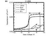
(3) Dependence of the shift of the flat band voltage VFB on the thickness of the underlying SiO2 film Next, with respect to the MIS structure of FIG. 4, the starting voltage is set to 10 V, and the sweep is made from +10 V → −10 V → + 10 V. CV characteristics were obtained. The results are shown in FIG.
図6によれば、AlON膜と基板との間に下地SiO2膜が介在した構造を有するMIS構造(<6nm、6nmおよび13nm)は、4H−SiC基板に直接AlON膜を形成した場合(「なし」)に比べて、フラットバンド電圧VFBのシフト量を低減できることが分かった。
(4)フラットバンド電圧VFBのシフト量の下地SiO2膜の厚さへの依存性
次に、上記(3)に倣って、開始電圧を変更した条件でもC−V特性を求めた。開始電圧の変更条件は、+5Vから+60Vまで5V刻みとした。このときの蓄積電圧(Accumulation Voltage)とフラットバンド電圧(Flatband Voltage)との関係を図7に示す。According to FIG. 6, the MIS structure (<6 nm, 6 nm, and 13 nm) having a structure in which the base SiO2 film is interposed between the AlON film and the substrate is obtained when the AlON film is formed directly on the 4H—SiC substrate (“ It was found that the shift amount of the flat band voltage VFB can be reduced as compared with “none”).
(4) Dependence of the shift amount of the flat band voltage VFB on the thickness of the underlying SiO2 film Next, in accordance with the above (3), the CV characteristics were also obtained under the conditions where the starting voltage was changed. The change condition of the starting voltage was set to 5V from + 5V to + 60V. FIG. 7 shows the relationship between the accumulated voltage and the flatband voltage at this time.
図7によれば、蓄積電圧が同じであれば、下地SiO2膜10が厚いほどフラットバンド電圧VFBのシフト量を低減できることが分かった。たとえば、蓄積電圧が45Vの場合、各MIS構造のシフト量は、「<6nm」=約9V、「6nm」=約5V、「13nm」=約1Vであることが分かった。
(5)フラットバンド電圧VFBのシフトのN組成への依存性
次に、フラットバンド電圧VFBのシフトのN組成への依存性を実証するため、具体的な実験を行った。実験サンプルとして、上記(2)に記載の方法に倣って、図4に示すMIS構造を作製した。ただし、AlON膜の成膜方法が異なる実験サンプルを3パターン作製した。採用した成膜方法は、CVD1法、CVD2法およびPVD法の3つである。得られたCVD1膜、CVD2膜およびPVD膜の組成をそれぞれ図8〜図10に示す。また、CVD1膜およびCVD2膜については、成膜後にPDAを行ったサンプル(CVD1+PDA、CVD2+PDA)も作製した。According to FIG. 7, it is found that if the storage voltage is the same, the shift amount of the flat band voltageVFB can be reduced as the base SiO2 film 10 is thicker. For example, when the storage voltage is 45 V, the shift amount of each MIS structure is found to be “<6 nm” = about 9 V, “6 nm” = about 5 V, and “13 nm” = about 1 V.
(5) Dependence of Shift of Flat Band Voltage VFB on N Composition Next, a specific experiment was performed to demonstrate the dependence of the shift of flat band voltage VFB on the N composition. As an experimental sample, the MIS structure shown in FIG. 4 was fabricated following the method described in (2) above. However, three patterns of experimental samples with different AlON film formation methods were prepared. There are three film forming methods employed, the
次に、上記(3)および(4)に記載の測定方法に倣って各サンプルのC−V特性を求めた。そして、得られたC−V特性に基づいて、蓄積電圧(Accumulation Voltage)とフラットバンド電圧(Flatband Voltage)との関係を調べた。結果を図11に示す。
図11によれば、CVD2膜に比べてN組成(濃度)が高いCVD1膜の方が、フラットバンド電圧VFBのシフト量を低減できることが分かった。たとえば、蓄積電圧が55Vの場合、CVD2膜のサンプルのシフト量が約15Vであるのに対し、CVD1膜のサンプルのシフト量は約10Vであった。また、成膜後のPDAの有無に関して、PDAを行った方が行わない場合に比べて、シフト量を低減できることが分かった。
(6)AlON膜によるフラットバンド電圧VFBの抑制効果
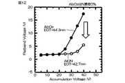
次に、上記(5)で得られたPDA膜を用いた場合のフラットバンド電圧VFBのシフト量が、Al2O3膜を用いた場合に比べてどの程度抑制されるかどうかを調べた。結果を図12に示す。Next, CV characteristics of each sample were obtained in accordance with the measurement methods described in (3) and (4) above. Then, based on the obtained CV characteristics, the relationship between the accumulated voltage (Accumulation Voltage) and the flatband voltage (Flatband Voltage) was examined. The results are shown in FIG.
According to FIG. 11, it was found that the shift amount of the flat band voltage VFB can be reduced in the
(6) Effect of suppressing flat band voltage VFB by AlON film Next, the shift amount of the flat band voltage VFB in the case of using the PDA film obtained in the above (5) uses the Al2 O3 film. We investigated how much it was suppressed compared to the case. The results are shown in FIG.
図12によれば、N組成が0%のAl2O3膜を用いた場合にはフラットバンド電圧VFBのシフト量が非常に大きくなることが分かった。この結果、ゲート絶縁膜にAlON膜を含めることによって、フラットバンド電圧VFBのシフトを抑制できることが分かった。したがって、AlON膜を含むゲート絶縁膜を有するMIS構造では、閾値電圧Vthのシフトを抑制することができる。
(7)フラットバンド電圧VFBと窒素組成との関係
次に、フラットバンド電圧VFBのシフトのN組成への依存性(蓄積電圧固定)を実証するため、実験サンプルとして、上記(2)に記載の方法に倣って、図4に示すMIS構造をSi基板上に作製した。実験サンプルは、N組成が異なるものを8種類作製した。そして、各サンプルのフラットバンド電圧VFBのシフトが、蓄積電圧Vaccが25Vおよび30Vのときにどのように変化するかを検証した。結果を図13に示す。なお、得られた検証結果は、Si基板上のデータであり、同様の検証をSiC基板上のMIS構造に行ったときの参考データである。図13から、N組成15%以上の場合にフラットバンド電圧VFBのシフトが少なくなるので、好ましい。また、N組成が大きいと誘電率が低下してしまうので、N組成が35%以下であると好ましい。According to FIG. 12, it was found that the shift amount of the flat band voltage VFB becomes very large when an Al2 O3 film having an N composition of 0% is used. As a result, it was found that the shift of the flat band voltageVFB can be suppressed by including an AlON film in the gate insulating film. Therefore, in the MIS structure having the gate insulating film including the AlON film, the shift of the threshold voltageVth can be suppressed.
(7) Relationship between Flat Band Voltage VFB and Nitrogen Composition Next, in order to demonstrate the dependency of the shift of the flat band voltage VFB on the N composition (fixed storage voltage), as an experimental sample, the above (2) Following the described method, the MIS structure shown in FIG. 4 was fabricated on a Si substrate. Eight types of experimental samples with different N compositions were prepared. Then, it was verified how the shift of the flat band voltage VFB of each sample changes when the storage voltage Vacc is 25V and 30V. The results are shown in FIG. The obtained verification result is data on the Si substrate, and is reference data when the same verification is performed on the MIS structure on the SiC substrate. From FIG. 13, when the N composition is 15% or more, the shift of the flat band voltageVFB is reduced, which is preferable. Moreover, since a dielectric constant will fall when N composition is large, it is preferable in N composition being 35% or less.
1 半導体装置
2 SiC基板
3 SiCエピタキシャル層
4 ゲートトレンチ
9 ゲート絶縁膜
10 下地SiO2膜
11 AlON膜
12 上側SiO2膜
13 ゲート電極
41 半導体装置
44 ゲート絶縁膜
45 ゲート電極
47 下地SiO2膜
48 AlON膜
49 上側SiO2膜1
Claims (11)
Translated fromJapanese前記半導体層に接するゲート絶縁膜と、
前記ゲート絶縁膜上に形成されたゲート電極とを含むMIS構造を有し、
前記ゲート絶縁膜は、窒素組成が5%〜40%のAlON層を含む、半導体装置。A semiconductor layer;
A gate insulating film in contact with the semiconductor layer;
A MIS structure including a gate electrode formed on the gate insulating film;
The gate insulating film includes a AlON layer having a nitrogen composition of 5% to 40%.
Priority Applications (3)
| Application Number | Priority Date | Filing Date | Title |
|---|---|---|---|
| JP2012265615AJP2014110402A (en) | 2012-12-04 | 2012-12-04 | Semiconductor device |
| PCT/JP2013/082390WO2014087975A1 (en) | 2012-12-04 | 2013-12-02 | Semiconductor device |
| US14/649,149US9397185B2 (en) | 2012-12-04 | 2013-12-02 | Semiconductor device |
Applications Claiming Priority (1)
| Application Number | Priority Date | Filing Date | Title |
|---|---|---|---|
| JP2012265615AJP2014110402A (en) | 2012-12-04 | 2012-12-04 | Semiconductor device |
Related Child Applications (1)
| Application Number | Title | Priority Date | Filing Date |
|---|---|---|---|
| JP2017096578ADivisionJP6346341B2 (en) | 2017-05-15 | 2017-05-15 | Semiconductor device |
Publications (1)
| Publication Number | Publication Date |
|---|---|
| JP2014110402Atrue JP2014110402A (en) | 2014-06-12 |
Family
ID=50883392
Family Applications (1)
| Application Number | Title | Priority Date | Filing Date |
|---|---|---|---|
| JP2012265615APendingJP2014110402A (en) | 2012-12-04 | 2012-12-04 | Semiconductor device |
Country Status (3)
| Country | Link |
|---|---|
| US (1) | US9397185B2 (en) |
| JP (1) | JP2014110402A (en) |
| WO (1) | WO2014087975A1 (en) |
Cited By (6)
| Publication number | Priority date | Publication date | Assignee | Title |
|---|---|---|---|---|
| WO2019009006A1 (en)* | 2017-07-07 | 2019-01-10 | パナソニック株式会社 | Semiconductor device |
| US10211301B1 (en) | 2017-11-22 | 2019-02-19 | Kabushiki Kaisha Toshiba | Semiconductor device, inverter circuit, driving device, vehicle, elevator, power supply circuit, and computer |
| US10256308B1 (en) | 2017-11-22 | 2019-04-09 | Kabushiki Kaisha Toshiba | Semiconductor device, power supply circuit, and computer |
| DE112017003591T5 (en) | 2016-07-15 | 2019-05-02 | Rohm Co., Ltd. | SEMICONDUCTOR DEVICE |
| JP2019102814A (en)* | 2017-12-01 | 2019-06-24 | インフィニオン テクノロジーズ アクチエンゲゼルシャフトInfineon Technologies AG | Silicon carbide semiconductor module including trench gate structure and shield region |
| JP2022190166A (en)* | 2018-01-17 | 2022-12-22 | ローム株式会社 | Semiconductor device and its manufacturing method |
Families Citing this family (3)
| Publication number | Priority date | Publication date | Assignee | Title |
|---|---|---|---|---|
| US9224854B2 (en) | 2013-10-03 | 2015-12-29 | Texas Instruments Incorporated | Trench gate trench field plate vertical MOSFET |
| JP6776205B2 (en)* | 2017-09-20 | 2020-10-28 | 株式会社東芝 | Manufacturing method of semiconductor devices |
| US20240290879A1 (en)* | 2023-02-27 | 2024-08-29 | Globalfoundries U.S. Inc. | Field-effect transistors with deposited gate dielectric layers |
Citations (5)
| Publication number | Priority date | Publication date | Assignee | Title |
|---|---|---|---|---|
| JP2002524860A (en)* | 1998-08-28 | 2002-08-06 | クリー インコーポレイテッド | Stacked dielectric in silicon carbide semiconductor structure |
| WO2003026019A1 (en)* | 2001-09-12 | 2003-03-27 | Nec Corporation | Semiconductor device and production method therefor |
| JP2005183597A (en)* | 2003-12-18 | 2005-07-07 | Nec Corp | Nitride semiconductor MIS field effect transistor |
| WO2011027831A1 (en)* | 2009-09-07 | 2011-03-10 | ローム株式会社 | Semiconductor device and process for production thereof |
| WO2012105611A1 (en)* | 2011-02-02 | 2012-08-09 | ローム株式会社 | Semiconductor power device and method for producing same |
Family Cites Families (1)
| Publication number | Priority date | Publication date | Assignee | Title |
|---|---|---|---|---|
| JP5519901B2 (en) | 2007-07-04 | 2014-06-11 | 三菱電機株式会社 | Silicon carbide field effect transistor and method of manufacturing the same |
- 2012
- 2012-12-04JPJP2012265615Apatent/JP2014110402A/enactivePending
- 2013
- 2013-12-02WOPCT/JP2013/082390patent/WO2014087975A1/enactiveApplication Filing
- 2013-12-02USUS14/649,149patent/US9397185B2/enactiveActive
Patent Citations (5)
| Publication number | Priority date | Publication date | Assignee | Title |
|---|---|---|---|---|
| JP2002524860A (en)* | 1998-08-28 | 2002-08-06 | クリー インコーポレイテッド | Stacked dielectric in silicon carbide semiconductor structure |
| WO2003026019A1 (en)* | 2001-09-12 | 2003-03-27 | Nec Corporation | Semiconductor device and production method therefor |
| JP2005183597A (en)* | 2003-12-18 | 2005-07-07 | Nec Corp | Nitride semiconductor MIS field effect transistor |
| WO2011027831A1 (en)* | 2009-09-07 | 2011-03-10 | ローム株式会社 | Semiconductor device and process for production thereof |
| WO2012105611A1 (en)* | 2011-02-02 | 2012-08-09 | ローム株式会社 | Semiconductor power device and method for producing same |
Non-Patent Citations (1)
| Title |
|---|
| 景井悠介,桐野嵩史,箕谷周平,中野佑紀,中村孝,細井卓治,志村考功,渡部平司: "18a−TJ−5 Al2O3/SiO2積層ゲート絶縁膜への窒素添加による4H−SiC MISデバイス", 2010年春季第57回応用物理学関係連合講演会講演予稿集, JPN6016038240, 3 March 2010 (2010-03-03), pages 15 - 284, ISSN: 0003413590* |
Cited By (18)
| Publication number | Priority date | Publication date | Assignee | Title |
|---|---|---|---|---|
| DE112017003591T5 (en) | 2016-07-15 | 2019-05-02 | Rohm Co., Ltd. | SEMICONDUCTOR DEVICE |
| US10833166B2 (en) | 2016-07-15 | 2020-11-10 | Rohm Co., Ltd. | Semiconductor device including an MIS structure |
| JPWO2019009006A1 (en)* | 2017-07-07 | 2020-05-07 | パナソニック株式会社 | Semiconductor device |
| JP7203727B2 (en) | 2017-07-07 | 2023-01-13 | パナソニックホールディングス株式会社 | semiconductor equipment |
| US11342428B2 (en) | 2017-07-07 | 2022-05-24 | Panasonic Holdings Corporation | Semiconductor device |
| WO2019009006A1 (en)* | 2017-07-07 | 2019-01-10 | パナソニック株式会社 | Semiconductor device |
| JP2019096719A (en)* | 2017-11-22 | 2019-06-20 | 株式会社東芝 | Semiconductor device, inverter circuit, driver, vehicle, lift, power supply circuit, and computer |
| US10535744B2 (en) | 2017-11-22 | 2020-01-14 | Kabushiki Kaisha Toshiba | Semiconductor device, power supply circuit, and computer |
| US10256308B1 (en) | 2017-11-22 | 2019-04-09 | Kabushiki Kaisha Toshiba | Semiconductor device, power supply circuit, and computer |
| US10211301B1 (en) | 2017-11-22 | 2019-02-19 | Kabushiki Kaisha Toshiba | Semiconductor device, inverter circuit, driving device, vehicle, elevator, power supply circuit, and computer |
| JP2019102814A (en)* | 2017-12-01 | 2019-06-24 | インフィニオン テクノロジーズ アクチエンゲゼルシャフトInfineon Technologies AG | Silicon carbide semiconductor module including trench gate structure and shield region |
| JP7283890B2 (en) | 2017-12-01 | 2023-05-30 | インフィニオン テクノロジーズ アクチエンゲゼルシャフト | Silicon carbide semiconductor module with trench gate structure and shield regions |
| US11855147B2 (en) | 2017-12-01 | 2023-12-26 | Infineon Technologies Ag | Method for producing a silicon carbide semiconductor component |
| US12324203B2 (en) | 2017-12-01 | 2025-06-03 | Infineon Technologies Ag | Method for producing a silicon carbide semiconductor component |
| JP2022190166A (en)* | 2018-01-17 | 2022-12-22 | ローム株式会社 | Semiconductor device and its manufacturing method |
| US11996449B2 (en) | 2018-01-17 | 2024-05-28 | Rohm Co., Ltd. | Semiconductor device with carbon-density-decreasing region |
| JP7512348B2 (en) | 2018-01-17 | 2024-07-08 | ローム株式会社 | Semiconductor device and its manufacturing method |
| JP2024111334A (en)* | 2018-01-17 | 2024-08-16 | ローム株式会社 | Semiconductor Device |
Also Published As
| Publication number | Publication date |
|---|---|
| US9397185B2 (en) | 2016-07-19 |
| US20150318372A1 (en) | 2015-11-05 |
| WO2014087975A1 (en) | 2014-06-12 |
Similar Documents
| Publication | Publication Date | Title |
|---|---|---|
| JP2014110402A (en) | Semiconductor device | |
| US10074728B2 (en) | Semiconductor device | |
| TWI578405B (en) | Wet chemical method for fabricating semiconductor devices with enhanced channel mobility | |
| JP5584823B2 (en) | Silicon carbide semiconductor device | |
| JP5982471B2 (en) | Field effect silicon carbide transistor | |
| KR102505057B1 (en) | Hybrid Gate Dielectrics for Semiconductor Power Devices | |
| JP2014192493A5 (en) | ||
| CN109478567B (en) | Semiconductor device with a plurality of semiconductor chips | |
| JP2015046444A (en) | Semiconductor device | |
| JP2022107025A (en) | Semiconductor equipment | |
| US20130248880A1 (en) | Semiconductor device and method for manufacturing the same | |
| US9978842B2 (en) | Semiconductor device and method for manufacturing the same | |
| JP7204547B2 (en) | semiconductor equipment | |
| JP6267706B2 (en) | Semiconductor device and manufacturing method thereof | |
| CN117457746B (en) | Trench gate type silicon carbide power device, manufacturing method thereof and semiconductor structure | |
| JP6500912B2 (en) | Silicon carbide semiconductor device and method of manufacturing silicon carbide semiconductor device | |
| JP5098293B2 (en) | Insulated gate type semiconductor device using wide band gap semiconductor and manufacturing method thereof | |
| JPWO2010110252A1 (en) | MOSFET and MOSFET manufacturing method | |
| JP2018129558A (en) | Semiconductor device | |
| JP6346341B2 (en) | Semiconductor device | |
| WO2017077780A1 (en) | Silicon carbide semiconductor device | |
| JP6945036B2 (en) | Semiconductor device | |
| JP2008053554A (en) | Electronic device and manufacturing method thereof | |
| JP2017188687A (en) | Operation method and design method for semiconductor device | |
| JP6092680B2 (en) | Semiconductor device and manufacturing method of semiconductor device |
Legal Events
| Date | Code | Title | Description |
|---|---|---|---|
| A621 | Written request for application examination | Free format text:JAPANESE INTERMEDIATE CODE: A621 Effective date:20151104 | |
| A131 | Notification of reasons for refusal | Free format text:JAPANESE INTERMEDIATE CODE: A131 Effective date:20161006 | |
| A521 | Request for written amendment filed | Free format text:JAPANESE INTERMEDIATE CODE: A523 Effective date:20161130 | |
| A02 | Decision of refusal | Free format text:JAPANESE INTERMEDIATE CODE: A02 Effective date:20170216 |