JP2014107730A - Signal processing device and amplifier - Google Patents
Signal processing device and amplifierDownload PDFInfo
- Publication number
- JP2014107730A JP2014107730AJP2012259732AJP2012259732AJP2014107730AJP 2014107730 AJP2014107730 AJP 2014107730AJP 2012259732 AJP2012259732 AJP 2012259732AJP 2012259732 AJP2012259732 AJP 2012259732AJP 2014107730 AJP2014107730 AJP 2014107730A
- Authority
- JP
- Japan
- Prior art keywords
- amplifier
- signal input
- signal
- switching
- sensor
- Prior art date
- Legal status (The legal status is an assumption and is not a legal conclusion. Google has not performed a legal analysis and makes no representation as to the accuracy of the status listed.)
- Ceased
Links
- 239000003990capacitorSubstances0.000description15
- 230000001133accelerationEffects0.000description10
- 230000003321amplificationEffects0.000description7
- 238000000034methodMethods0.000description7
- 238000003199nucleic acid amplification methodMethods0.000description7
- 238000010586diagramMethods0.000description6
- 238000005259measurementMethods0.000description4
- 238000004088simulationMethods0.000description3
- 230000004048modificationEffects0.000description2
- 238000012986modificationMethods0.000description2
- 229920006395saturated elastomerPolymers0.000description2
- 230000003071parasitic effectEffects0.000description1
- 238000004904shorteningMethods0.000description1
Images


Classifications
- G—PHYSICS
- G01—MEASURING; TESTING
- G01P—MEASURING LINEAR OR ANGULAR SPEED, ACCELERATION, DECELERATION, OR SHOCK; INDICATING PRESENCE, ABSENCE, OR DIRECTION, OF MOVEMENT
- G01P15/00—Measuring acceleration; Measuring deceleration; Measuring shock, i.e. sudden change of acceleration
- G01P15/14—Measuring acceleration; Measuring deceleration; Measuring shock, i.e. sudden change of acceleration by making use of gyroscopes
- G—PHYSICS
- G01—MEASURING; TESTING
- G01C—MEASURING DISTANCES, LEVELS OR BEARINGS; SURVEYING; NAVIGATION; GYROSCOPIC INSTRUMENTS; PHOTOGRAMMETRY OR VIDEOGRAMMETRY
- G01C19/00—Gyroscopes; Turn-sensitive devices using vibrating masses; Turn-sensitive devices without moving masses; Measuring angular rate using gyroscopic effects
- G01C19/56—Turn-sensitive devices using vibrating masses, e.g. vibratory angular rate sensors based on Coriolis forces
- G01C19/5776—Signal processing not specific to any of the devices covered by groups G01C19/5607 - G01C19/5719
- G—PHYSICS
- G01—MEASURING; TESTING
- G01P—MEASURING LINEAR OR ANGULAR SPEED, ACCELERATION, DECELERATION, OR SHOCK; INDICATING PRESENCE, ABSENCE, OR DIRECTION, OF MOVEMENT
- G01P15/00—Measuring acceleration; Measuring deceleration; Measuring shock, i.e. sudden change of acceleration
- H—ELECTRICITY
- H03—ELECTRONIC CIRCUITRY
- H03F—AMPLIFIERS
- H03F3/00—Amplifiers with only discharge tubes or only semiconductor devices as amplifying elements
- H03F3/45—Differential amplifiers
- H03F3/45071—Differential amplifiers with semiconductor devices only
- H03F3/45076—Differential amplifiers with semiconductor devices only characterised by the way of implementation of the active amplifying circuit in the differential amplifier
- H03F3/45179—Differential amplifiers with semiconductor devices only characterised by the way of implementation of the active amplifying circuit in the differential amplifier using MOSFET transistors as the active amplifying circuit
- H03F3/45183—Long tailed pairs
Landscapes
- Engineering & Computer Science (AREA)
- Physics & Mathematics (AREA)
- General Physics & Mathematics (AREA)
- Power Engineering (AREA)
- Signal Processing (AREA)
- Radar, Positioning & Navigation (AREA)
- Remote Sensing (AREA)
- Amplifiers (AREA)
Abstract
Description
Translated fromJapanese本発明は、センサの出力信号を増幅する技術に関する。 The present invention relates to a technique for amplifying an output signal of a sensor.
近年、地磁気センサや加速度センサなどの各種センサの利用が急速に普及している。例えば、スマートフォンなどの携帯端末にこの種のセンサを設け、センサにより検出された方位や加速度を利用して各種のサービスを提供するといった具合である。この種のセンサの出力信号は微弱であるため、増幅器による増幅を経て使用されることが一般的である(特許文献1参照)。 In recent years, the use of various sensors such as a geomagnetic sensor and an acceleration sensor has been rapidly spreading. For example, this type of sensor is provided in a mobile terminal such as a smartphone, and various services are provided using the direction and acceleration detected by the sensor. Since the output signal of this type of sensor is weak, it is generally used after being amplified by an amplifier (see Patent Document 1).
従来、センサの出力信号を増幅器により増幅する場合、増幅可能な周波数帯域を固定で動作させる(すなわち、高速動作させる場合には増幅器を広帯域で動作させる)ことが多かった。その理由は以下の通りである。図7(a)には、増幅器を狭帯域で動作させた場合と広帯域(狭帯域の4倍の帯域幅)で動作させた場合の各々における増幅器の周波数特性を示すグラフが図示されており、図7(b)には、狭帯域の場合と広帯域の場合の各々における増幅器のセトリング時間を示すグラフが図示されている。セトリング時間とは、矩形波状のステップ入力を増幅器に与えてから、当該増幅器の出力が収束するまでに要する時間(すなわち、増幅器の出力信号が安定するまでに要する時間)である。図7(b)に示すように、広帯域の場合の方がセトリング時間は短くなる。物理的な状態をセンサで検出し、センサの出力信号を用いて何らかの装置を制御する場合、状態の変化を短い遅延で検出して制御に反映させるためには、センサの出力信号を増幅する増幅器を広帯域で動作させ、セトリング時間を短くする必要がある。しかしながら、増幅器を広帯域で動作させるとノイズも増幅され、増幅器を狭帯域で動作させる場合に比較して、増幅後の信号のS/N比が低下し、センサの出力信号の微小な変化を拾えなくなるといった問題がある。 Conventionally, when an output signal of a sensor is amplified by an amplifier, the frequency band that can be amplified is fixedly operated (that is, the amplifier is operated in a wide band when operating at a high speed). The reason is as follows. FIG. 7A shows a graph showing the frequency characteristics of the amplifier when the amplifier is operated in a narrow band and when the amplifier is operated in a wide band (four times the bandwidth of the narrow band). FIG. 7B shows a graph showing the settling time of the amplifier in each of the narrow band case and the wide band case. The settling time is the time required for the output of the amplifier to converge after giving the rectangular wave step input to the amplifier (that is, the time required for the output signal of the amplifier to become stable). As shown in FIG. 7B, the settling time is shorter in the case of a wide band. An amplifier that amplifies the output signal of a sensor in order to detect a change in the state with a short delay and reflect it in the control when detecting a physical state with a sensor and controlling any device using the output signal of the sensor Must be operated in a wide band and settling time must be shortened. However, when the amplifier is operated in a wide band, noise is also amplified, and compared with the case where the amplifier is operated in a narrow band, the S / N ratio of the amplified signal is lowered, and a minute change in the output signal of the sensor can be picked up. There is a problem of disappearing.
本発明は上記課題に鑑みてなされたものであり、センサの出力信号を増幅器により増幅して利用する際に、増幅器の出力信号が安定するまでに要する時間が長くなることを避けつつ、S/N比を向上させることを解決課題とする。 The present invention has been made in view of the above problems. When the output signal of a sensor is amplified by an amplifier and used, the time required for the output signal of the amplifier to become stable is prevented from becoming long. The problem to be solved is to improve the N ratio.
上記課題を解決するために、本発明に係る信号処理装置は、帯域幅の切り換えが可能な増幅器と、前記増幅器への信号入力の開始から一定時間は前記増幅器を広帯域で動作させ、その後、前記増幅器を狭帯域で動作させる制御部とを有することを特徴とする。また、信号処理装置に用いる増幅器は、帯域幅の切り換えが可能な増幅器であって、当該増幅器への信号入力の開始を検知し、信号入力の開始から一定時間は広帯域で動作し、その後狭帯域で動作するものであっても良い。 In order to solve the above problems, a signal processing apparatus according to the present invention includes an amplifier capable of switching a bandwidth, and operating the amplifier in a wide band for a predetermined time from the start of signal input to the amplifier. And a control unit for operating the amplifier in a narrow band. The amplifier used in the signal processing device is an amplifier capable of switching the bandwidth, detects the start of signal input to the amplifier, operates for a certain period of time from the start of signal input, and then operates in a narrow band. It may be one that operates on.
本発明の信号処理装置に含まれる増幅器によりセンサの出力信号を増幅するようにすれば、例えば電源投入などによってセンサへの給電が開始され当該センサから増幅器への信号入力が開始されると、当該増幅器は信号入力の開始から一定時間の間は広帯域で動作する。このため、当該増幅器を狭帯域で動作する場合に比較してセトリング時間は短くなる。そして、信号入力開始から一定時間経過後は上記増幅器を狭帯域で動作させるため、広帯域で動作させ続ける場合に比較してS/N比を高くすることができる。このように本発明の信号処理装置によれば、センサの出力信号を増幅器により増幅して利用する際に、増幅器の出力信号が安定するまでに要する時間が長くなることを避けつつ、S/N比を向上させることができる。 When the output signal of the sensor is amplified by the amplifier included in the signal processing device of the present invention, for example, when power supply to the sensor is started by turning on the power and the signal input from the sensor to the amplifier is started, The amplifier operates in a wide band for a certain time from the start of signal input. Therefore, the settling time is shorter than when the amplifier is operated in a narrow band. Since the amplifier is operated in a narrow band after a lapse of a certain time from the start of signal input, the S / N ratio can be increased as compared with a case where the amplifier is continuously operated in a wide band. As described above, according to the signal processing device of the present invention, when the output signal of the sensor is amplified and used by the amplifier, the time required for the output signal of the amplifier to become stable is avoided, and the S / N The ratio can be improved.
ここで、上記一定時間の長さについては、広帯域で動作している状態の増幅器にステップ入力を与えてから、増幅器の出力信号が当該ステップ入力に応じた収束値の99%程度になるまでの時間を実測(或いは数値シミュレーション)により求め、当該時間の長さを上記一定時間として用いるようにすれば良い。ここで、1パーセント程度の余裕を持たせたのは、信号入力開始時点から広帯域および狭帯域での動作を経て増幅器の出力信号が安定するまでに要する時間(トータルのセトリング時間)を短くするためである。この点については後に詳細に説明する。 Here, with respect to the length of the predetermined time, the step input is given to the amplifier operating in a wide band until the output signal of the amplifier reaches about 99% of the convergence value corresponding to the step input. What is necessary is just to obtain | require time by actual measurement (or numerical simulation), and to use the length of the said time as said fixed time. Here, the margin of about 1% is provided in order to shorten the time (total settling time) required for the output signal of the amplifier to become stable through the operation in a wide band and a narrow band from the start of signal input. It is. This point will be described in detail later.
より好ましい態様においては、複数のセンサの各々を前記増幅器に対する信号入力元として選択するとともに、当該選択した信号入力元からの信号入力の開始を契機として前記増幅器を広帯域で動作させる処理を前記制御部に実行させる態様が考えられる。本態様によれば、増幅器を狭帯域のまま動作させ続ける場合に比較してセトリング時間を短くすることができる。なお、信号入力元の切り換え前後で切り換え前の信号入力元と切り換え後の信号入力元が各々同じ値の信号を出力している場合には、増幅器の増幅率を変化させる(換言すれば、増幅器の内部状態を変化させる)必要はなく、さらには、増幅器の帯域幅を広帯域に切り換えてセトリングを行う必要もない。このため、複数のセンサの各々を前記増幅器に対する信号入力元として選択するとともに、信号入力元の切り換えに応じて増幅器の内部状態が変化する場合に限って当該選択した信号入力元からの信号入力の開始を契機として増幅器を広帯域で動作させる処理を制御部に実行させても勿論良い。ところで、信号入力元の切り換え前後で切り換え前の信号入力元と切り換え後の信号入力元が各々同じ値の信号を出力していることは稀である。このため、信号入力元の切り換えが発生する毎に増幅器の内部状態に変化が生じたか否かを問わずに増幅器の帯域幅を広帯域に切り換える処理を制御部に実行させたとしても特段の問題は生じず、増幅器の内部状態の変化の有無の判定を行わない分だけ制御部の処理が簡略化される。さらに好ましい態様としては、選択した信号入力元が予め定められた種類のセンサである場合には、当該信号入力元からの信号入力の開始から一定時間後に前記増幅器の帯域幅を狭帯域に切り換える処理を制御部に実行させる態様が考えられる。例えば、上記複数のセンサに地磁気センサと加速度センサが含まれている場合には、地磁気センサが信号入力元として選択された場合には上記狭帯域への切り換えを制御部に実行させるのである。地磁気センサの出力信号は加速度センサの出力信号に比較して微弱であることが多く、ノイズの影響が大きいと考えられるからである。 In a more preferred aspect, a process of selecting each of a plurality of sensors as a signal input source for the amplifier and causing the amplifier to operate in a wide band with a start of signal input from the selected signal input source as a trigger. The mode to be executed is conceivable. According to this aspect, the settling time can be shortened as compared with the case where the amplifier is continuously operated in a narrow band. If the signal input source before switching and the signal input source after switching output the same value before and after switching the signal input source, the amplification factor of the amplifier is changed (in other words, the amplifier It is not necessary to settling by switching the bandwidth of the amplifier to a wide band. For this reason, each of the plurality of sensors is selected as a signal input source for the amplifier, and only when the internal state of the amplifier changes according to the switching of the signal input source, the signal input from the selected signal input source. Of course, it is also possible to cause the control unit to execute processing for operating the amplifier in a wide band with the start as a trigger. By the way, it is rare that the signal input source before switching and the signal input source after switching output signals of the same value before and after switching of the signal input source. For this reason, even if the control unit executes the process of switching the bandwidth of the amplifier to a wide band regardless of whether or not the internal state of the amplifier has changed every time the signal input source is switched, there is a particular problem. It does not occur, and the processing of the control unit is simplified to the extent that it is not determined whether there is a change in the internal state of the amplifier. As a more preferable aspect, when the selected signal input source is a sensor of a predetermined type, a process of switching the bandwidth of the amplifier to a narrow band after a predetermined time from the start of signal input from the signal input source. A mode in which the control unit is executed is conceivable. For example, when the plurality of sensors include a geomagnetic sensor and an acceleration sensor, the control unit is caused to perform switching to the narrow band when the geomagnetic sensor is selected as a signal input source. This is because the output signal of the geomagnetic sensor is often weaker than the output signal of the acceleration sensor, and it is considered that the influence of noise is large.
以下、図面を参照しつつ、本発明の実施形態について説明する。
<1.第1実施形態>
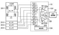
図1は、本発明の第1実施形態の信号処理装置10の構成例を示すブロック図である。
信号処理装置10は、センサ20−1〜20−4の各々を信号入力元として順次選択し、選択した信号入力元から与えられる差動信号を増幅してA/D変換器30に供給する。センサ20−1、20−2および20−3の各々は地磁気センサであり、同一の構成である。図1では、センサ20−1についてのみ具体的な構成例が図示されている。これら地磁気センサは、4個の巨大磁気抵抗素子(Giant Magneto Resistive effct)GMRをブリッジ接続して構成されている。本実施形態では、センサ20−1、20−2および20−3によって3軸の地磁気センサが形成される。センサ20−4は3軸の加速度センサであり、各軸方向の加速度の成分を表す3組の差動信号を出力する。Hereinafter, embodiments of the present invention will be described with reference to the drawings.
<1. First Embodiment>
FIG. 1 is a block diagram showing a configuration example of a
The
信号処理装置10は、図1に示すように、スイッチ110−n(n=1〜4)およびスイッチ112−n(n=1〜4)と、増幅器120と、制御部130と、を含んでいる。スイッチ110−nはセンサ20−nの一方の信号出力端と増幅器120の一方の信号入力端の間に介挿されており、スイッチ112−nはセンサ20−nの他方の信号出力端と増幅器120の他方の信号入力端の間に介挿されている。スイッチ110−nおよびスイッチ112−nのオン/オフの切り換えは、制御部130から出力される選択信号SEL−nによって行われる。例えば、選択信号SEL−nがHレベルであればスイッチ110−nおよびスイッチ112−nは共にオンとなり、選択信号SEL−nがLレベルであればスイッチ110−nおよびスイッチ112−nは共にオフとなる、といった具合である。本実施形態では、スイッチ110−nおよびスイッチ112−nのオン/オフ制御によって、増幅器120に対する信号入力元の切り換えが実現される。例えば、センサ20−1を信号入力元として選択する場合には、スイッチ110−1およびスイッチ112−1をオンにし、かつスイッチ110−n(n=2〜4)およびスイッチ112−n(n=2〜4)をオフにすれば良い。 As shown in FIG. 1, the
増幅器120は、図1に示すように、オペアンプ122aおよび122bと、抵抗124、126および128を含んでいる。オペアンプ122aの正相入力端には、スイッチ110−n(n=1〜4)およびスイッチ112−n(n=1〜4)のオン/オフ制御により選択された信号入力元の出力する差動信号の一方が与えられ、オペアンプ122bの正相入力端には、同差動信号の他方が与えられる。オペアンプ122aの出力端と逆相入力端との間には抵抗124が介挿されており、オペアンプ122bの出力端と逆相入力端との間には抵抗126が介挿されている。そして、オペアンプ122aの逆相入力端とオペアンプ122bの逆相入力端とは、抵抗128を介して接続されている。抵抗124および抵抗126の各々の抵抗値がRであり、抵抗128の抵抗値がrであり、オペアンプ122aの正相入力端には電圧Vpが与えられ、オペアンプ122bの正相入力端には電圧Vnが与えられるとすると、増幅器120は電圧差(Vp−Vn)を以下の式(1)に示すように増幅して出力する。なお、以下の式(1)において電圧Vopはオペアンプ122aの出力電圧であり、電圧Vonはオペアンプ122bの出力電圧である。
Vop−Von=(2R/r+1)(Vp−Vn)・・・(1)
本実施形態では、抵抗124および抵抗126の各々の抵抗値Rと抵抗128の抵抗値rを調整することで増幅器120の増幅率が制御される。抵抗124、126および128の各々の抵抗値の調整は制御部130によって行われる。As shown in FIG. 1, the
Vop−Von = (2R / r + 1) (Vp−Vn) (1)
In the present embodiment, the amplification factor of the
本実施形態では、オペアンプ122aおよび122bとして、帯域幅の制御が可能なオペアンプが用いられている。このため、増幅器120の帯域幅も可変である。本実施形態では、制御部130から与えられる帯域制御信号SBに応じてオペアンプ122aおよび122bの帯域幅を切り換えることで、増幅器120の帯域幅の切り換えが実現される。具体的には、Hレベルの帯域制御信号SBが制御部130から与えられた場合には、オペアンプ122aおよび122bは広帯域で動作し(すなわち、増幅器120は広帯域で動作し)、Lレベルの帯域制御信号SBが制御部130から与えられた場合には、オペアンプ122aおよび122bは狭帯域で動作する(すなわち、増幅器120は狭帯域で動作する)、といった具合である。 In this embodiment, operational amplifiers capable of controlling the bandwidth are used as the
オペアンプ122aの構成とオペアンプ122bの構成は同一である。よって、以下では、オペアンプ122aと122bを区別する必要がない場合には「オペアンプ122」と表記する。図2は、オペアンプ122の構成例を示す回路図である。図2に示すように、オペアンプ122は、差動増幅回路1210と、オペアンプ122の出力段を為す出力回路1220と、差動増幅回路1210および出力回路1220に流れる電流を制御するための電流制御部1230とを含んでいる。 The configuration of the
差動増幅回路1210は、オペアンプ122の正相入力端に与えられる信号IPと同逆相入力端に与えられる信号INの差動増幅を行う回路である。図2に示すように、差動増幅回路1210は、PチャネルトランジスタP1およびP2と、NチャネルトランジスタN1、N2およびN4により構成されている。PチャネルトランジスタP1およびP2の各々のソースは高電位側電源VPPに接続されており、各々のゲートはPチャネルトランジスタP1のドレインに接続されている。PチャネルトランジスタP1のドレインにはNチャネルトランジスタN1のドレインが接続されており、PチャネルトランジスタP2のドレインにはNチャネルトランジスタN2のドレインが接続されている。PチャネルトランジスタP2のドレインとNチャネルトランジスタN2のドレインの共通接続点は差動増幅回路1210の出力端となっている。NチャネルトランジスタN1およびN2の各々のソースは共通接続されており、この共通接続点と低電位側電源VSSの間にはNチャネルトランジスタN4が介挿されている。NチャネルトランジスタN1およびN2の各々のゲートには信号INおよびIPが夫々与えられ、NチャネルトランジスタN1とN2は差動トランジスタペアを構成する。PチャネルトランジスタP1およびP2は、それぞれNチャネルトランジスタN1およびN2の負荷となっているとともに、カレントミラー回路を形成する。 The
出力回路1220は、高電位側電源VDDと低電位側電源VSSの間に直列に介挿されPチャネルトランジスタP3およびNチャネルトランジスタN3を含んでおり、PチャネルトランジスタP3のドレインとNチャネルトランジスタN3のドレインの共通接続点が出力回路1220の出力端となっている。PチャネルトランジスタP3のゲートは差動増幅回路1210の出力端に接続されており、両者の共通接続点と出力回路1220の出力端との間には、位相補償のための抵抗1222およびキャパシタ1224が直列に介挿されている。 The
電流制御部1230は、出力電流の電流値を切り換え可能な電流源回路1232と低電位側電源VSSに間にNチャネルトランジスタN5を介挿して構成されている。電流源回路1232には、帯域制御信号SBが与えられる。電流源回路1232は、Lレベルの帯域制御信号SBを与えられた場合には電流値I1の電流を出力し、Hレベルの帯域制御信号を与えられた場合には電流値I1よりも大きい電流値I2(例えば、I2=2×I1)の電流を出力する。NチャネルトランジスタN5のゲートは、電流源回路1232とNチャネルトランジスタN5のドレインの共通接続点に接続されており、この共通接続点にはNチャネルトランジスタN3およびN4の各々のゲートが接続されている。つまり、NチャネルトランジスタN5は、NチャネルトランジスタN3とカレントミラー回路を形成するとともに、NチャネルトランジスタN4とカレントミラー回路を形成する。このため、電流源回路1232の出力電流の電流値をIrefとすると、差動増幅回路1210には、当該電流値IrefにNチャネルトランジスタN5とN4のトランジスタサイズの比を乗算した電流値の電流が流れ、出力回路1220にはNチャネルトランジスタN5とN3のトランジスタサイズの比を乗算した電流値の電流が流れる。出力回路1220および差動増幅回路1210に流れる電流が大きい程、各トランジスタのゲートに付随する寄生容量に高速に充電できる。このため、電流が大きい程、オペアンプ122の帯域幅は広くなる。よって、オペアンプ122は、Hレベルの帯域制御信号SBを与えられると広帯域で動作し、Lレベルの帯域制御信号SBを与えられると狭帯域で動作するのである。 The
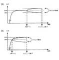
制御部130は、増幅器120への信号入力の開始から一定時間Tの間は当該増幅器120を広帯域で動作させ、その後、狭帯域で動作させる制御を行う。より詳細に説明すると、センサ20−n(n=1〜4)、信号処理装置10およびA/D変換器30を含むシステムの電源投入を契機として、制御部130は、まず、センサ20−1を選択し、当該センサ20−1の出力信号の最大値がA/D変換器30の入力可能電圧の最大値に対応するように増幅器120の増幅率を設定する。これにより、センサ20−1から増幅器120への信号入力が開始される。制御部130は、電源投入後一定時間Tの間(すなわち、センサ20−1からの信号入力開始から一定時間Tの間)、帯域制御信号SBをHレベルとし、その後、帯域制御信号をLレベルとする(図3参照)。 The
その結果、電源投入から一定時間Tが経過するまでの間は、増幅器120は広帯域で動作し、その後、狭帯域で動作する。なお、一定時間Tの長さについては、広帯域で動作している状態の増幅器120にステップ入力を与えてから増幅器120の出力が収束値の99%程度となるまでの時間を予め実測(あるいは数値シミュレーション)により求め、当該時間の長さを一定時間Tとして用いるようにすれば良い。ここで、1パーセント程度の余裕を持たせた理由は以下の通りである。図4(a)に示すように、増幅器120を広帯域で動作させ、増幅器120の出力が飽和するのを待って広帯域から狭帯域への切り換えを行うことは勿論可能である。例えば、増幅器120の出力が十分に飽和するまでの時間を実測(あるいは数値シミュレーション)により求め、この時間の長さを一定時間Tとして用いるようにすれば良い。しかしながら、この場合、広帯域から狭帯域への帯域切り換えによって増幅器のオフセットが変動し、図4(a)に示すように、狭帯域への切り換え後に増幅器120の出力が飽和するのを待たねばならない。これに対して、図4(b)に示すように、増幅器120の出力が収束値の99%程度に達したときに広帯域から狭帯域へ切り換えるようにすれば、トータルのセトリング時間を短くすることができる。このように、トータルのセトリング時間を短くするため、1%程度の余裕を持たせて一定時間Tの長さを定めたのである。 As a result, the
図7(b)に示したように、増幅器は広帯域で動作させた場合の方が狭帯域で動作させた場合に比較して、セトリング時間が短くなるものの、S/N比は低下する。この点は、増幅器120についても同様である。本実施形態において、電源投入後一定時間Tに亙って増幅器120を広帯域で動作させるのはセットリング時間を短くするためである。そして、一定時間Tの経過後増幅器120を狭帯域で動作させるのは、増幅器120の出力信号におけるS/N比を高くするためである。 As shown in FIG. 7B, although the settling time is shorter when the amplifier is operated in a wide band than when it is operated in a narrow band, the S / N ratio is lowered. This also applies to the
以上説明したように電源投入時の増幅器120のセットリングを完了すると、制御部130は、後段回路から指示等に応じてスイッチ110−n(n=1〜4)およびスイッチ112−n(n=1〜4)のオン/オフを切り換えて増幅器120に対する信号入力元を切り換える。この切り換えの際に、制御部130は帯域制御信号SBをHレベルに切り換え、増幅器120を再度広帯域で動作させる。そして、制御部130は信号入力元の切り換えから一定時間経過後に帯域制御信号SBをLレベルに切り換え、増幅器120を狭帯域で動作させる。つまり、本実施形態では、増幅器120に対する信号入力元を切り換える毎に増幅器120を一旦広帯域で動作させ、信号入力元の切り換えから一定時間が経過した時点で増幅器120の帯域幅を狭帯域に切り換える処理が制御部130によって実行される。前述したように、信号入力元の切り換えに伴うトータルのセトリング時間を短くしつつ、高いS/N比を得られるようにするためである。もっとも、信号入力元の切り換え前後で切り換え前の信号入力元と切り換え後の信号入力元が各々同じ値の信号を出力している場合には、増幅器120の増幅率を変化させる(換言すれば、増幅器120の内部状態を変化させる)必要はなく、増幅器120を再度セトリングする必要はない。したがって、信号入力元の切り換えに応じて増幅器120の内部状態が変化する場合にのみ、信号入力の開始を契機として増幅器120を広帯域で動作させ、一定時間経過後に増幅器120の帯域幅を狭帯域に切り換える処理を制御部130に実行させることも勿論考えられる。しかし、信号入力元の切り換え前後で切り換え前の信号入力元と切り換え後の信号入力元が各々同じ値の信号を出力していることは稀であり、信号入力元の切り換えが発生する毎に増幅器120の内部状態に変化が生じたか否かを問わずに増幅器の帯域幅を一旦広帯域に切り換え、一定時間経過後に狭帯域に切り換える処理を制御部130に実行させたとしても特段の問題は生じず、制御部130に実行させる処理を簡略化することができる。このため、本実施形態では、増幅器120に対する信号入力元を切り換える毎に増幅器120を一旦広帯域で動作させ、信号入力元の切り換えから一定時間が経過した時点で増幅器120の帯域幅を狭帯域に切り換える処理を制御部130に実行させるようにしたのである。また、信号入力元の切り換えが発生する毎に増幅器120を広帯域で動作させるものの、信号入力の開始から一定時間T経過後の狭帯域への切り換えについては、新たな信号入力元が予め定められた種類のセンサである場合に実行するようにしても良い。例えば、信号入力元を加速度センサに切り換えた場合には狭帯域への切り換えを行わず、地磁気センサに切り換えた場合には狭帯域への切り換えを行うといった具合である。地磁気センサの出力信号は加速度センサの出力信号に比較して微弱であることが多く、ノイズの影響が大きいと考えられる一方、加速度センサについてはノイズの影響が小さく、増幅器120を広帯域のまま動作させ続けても大きな問題は生じないと考えられるからである。 As described above, when the settling of the
このように、本実施形態によれば、センサ20−n(n=1〜4)の各々の出力信号を増幅器120により増幅してA/D変換器30に与える際に、増幅器120の出力信号が安定するまでに要する時間が長くなることを避けつつ、S/N比を向上させることが可能になる。また、本実施形態によれば、増幅器120への信号入力開始から出力信号が安定するまでに要する時間を短くすることができるため、センサ等による測定時に回路を起動して測定を行い、測定し終わったら回路を停止するような使用法に有利となる。 As described above, according to the present embodiment, when the output signals of the sensors 20-n (n = 1 to 4) are amplified by the
<2.第2実施形態>
次いで本発明の第2実施形態について説明する。本実施形態は、センサ20−nの出力信号を増幅する増幅器を、前掲図2の構成のオペアンプ122に換えて図5に示すオペアンプ222を用いて構成した点が第1実施形態と異なる。図5では、図2におけるものと同一の構成要素には同一の符号が付されている。図2と図5を対比すれば明らかなように、オペアンプ222は、電流制御部1230に換えて電流制御部2230を有している点がオペアンプ122と異なる。そして、電流制御部2230は、電流源回路1232に換えて電流源回路2232を設けた点と、NチャネルトランジスタN5´、スイッチ2234aおよび2234bを新たに設けた点が電流制御部1230と異なる。<2. Second Embodiment>
Next, a second embodiment of the present invention will be described. This embodiment is different from the first embodiment in that an amplifier that amplifies the output signal of the sensor 20-n is configured using an
電流源回路2232は、定電流源回路であり、固定の電流値の電流を出力する。電流源回路2232とNチャネルトランジスタN5のドレインの共通接続点と低電位側電源VSSとの間には、スイッチ2234aおよび2234bが直列に介挿されている。また、当該共通接続点と低電位側電源VSSとの間にはNチャネルトランジスタN5´が介挿されている。そして、NチャネルトランジスタN5´のゲートは、スイッチ2234aとスイッチ2234bの共通接続点に接続されている。 The
スイッチ2234aおよび2234bは帯域制御信号SBの信号レベルに応じてオン/オフが切り換えられるスイッチである。本実施形態では、Hレベルの帯域制御信号SBが与えられた場合には、スイッチ2234aはオフに、スイッチ2234bはオンになる。逆に、Lレベルの帯域制御信号SBが与えられた場合には、スイッチ2234aはオンに、スイッチ2234bはオフになる。スイッチ2234aをオフとし、スイッチ2234bをオンとした状態(第1の状態)では、NチャネルトランジスタN5´はオフとなる。この様態では、電流源回路2232の出力電流は全てNチャネルトランジスタN5を介して低電位側電源VSSに流れる。 The
これに対して、スイッチ2234aをオンとし、スイッチ2234bをオフとした状態(第2の状態)では、NチャネルトランジスタN5´はオンとなり、電流源回路2232の出力電流はNチャネルトランジスタN5およびN5´の各々を介して低電位側電源VSSに流れる。つまり、NチャネルトランジスタN5´とNチャネルトランジスタN5が同じサイズの場合には、第2の状態においては、NチャネルトランジスタN5に流れる電流の電流値は第1の状態の半分になり、NチャネルトランジスタN3およびNチャネルトランジスタN4の各々に流れる電流の電流値も半分になる。つまり、本実施形態では、スイッチ2234aおよびスイッチ2234bのオン/オフを切り替えることで、出力回路1220および差動増幅回路1210に流れる電流の電流値が切り換えられ、オペアンプ220を含む増幅器の帯域幅が切り替えられる。 On the other hand, in a state where the
本実施形態においても、電源投入を契機としてセンサ20−1を選択し、図3に示すように帯域制御信号SBの信号値を切り換える処理を制御部130に実行させることで、本実施形態の増幅器の出力信号が安定するまでに要する時間が長くなることを避けつつ、S/N比の低下を回避することが可能になる。 Also in the present embodiment, the sensor 20-1 is selected when the power is turned on, and the
<3.第3実施形態>
上述した第1および第2実施形態では、センサ20−nの出力信号を増幅するための増幅器に含まれるオペアンプの差動増幅回路および出力回路に流れる電流の電流値を切り換えることで、当該増幅器の帯域幅を切り換える場合について説明した。しかし、オペアンプとともに増幅器を形成する帰還抵抗および入力抵抗の抵抗値を切り換えることで帯域幅の切り換えを実現しても良い。これら抵抗値の切り換えにより帯域幅の切り換えを実現する構成の一例としては、図1における増幅器120に換えて、図6に示す増幅器320を用いる構成が考えられる。<3. Third Embodiment>
In the first and second embodiments described above, by switching the current value of the current flowing through the differential amplifier circuit and the output circuit of the operational amplifier included in the amplifier for amplifying the output signal of the sensor 20-n, The case of switching the bandwidth has been described. However, switching of the bandwidth may be realized by switching the resistance values of the feedback resistor and the input resistor that form an amplifier together with the operational amplifier. As an example of a configuration for realizing the switching of the bandwidth by switching the resistance values, a configuration using the
増幅器320は、図6に示すように、オペアンプ322aおよび322bと、抵抗324a〜324iと、スイッチ326a〜326fと、キャパシタ328aおよび328bを含んでいる。抵抗324a〜324fの各々の抵抗値は何れもRであり、抵抗324g〜324iの各々の抵抗値は何れもrである。また、キャパシタ328aおよび328bの各々の容量は共にCである。なお、抵抗324a〜324fの各々の抵抗値が全て同じである必要はなく、また、抵抗324g〜324iの各々の抵抗値も全て同じである必要はない。抵抗324aおよび抵抗324fの各々の抵抗値をR1、抵抗324bおよび抵抗324eの各々の抵抗値をR2、抵抗324cおよび抵抗324dの各々の抵抗値をR3、抵抗324g、324h、324iのそれぞれの抵抗値をr1、r2、r3としたときに、R1:R2:R3=r1:r2:r3となっていれば良い。 As shown in FIG. 6, the
オペアンプ322aおよび322bは、第1実施形態におけるオペアンプ122や第2実施形態におけるオペアンプ222とは異なり、帯域幅を切り換えるための構成を有していない。オペアンプ322aの出力端と逆相入力端の間にはキャパシタ328aが介挿されている。オペアンプ322aの逆相入力端およびキャパシタ328aの共通接続点とオペアンプ322aの出力端の間には、抵抗324a、324bおよび324cが直列に介挿されている。そして、抵抗324aおよび324bの共通接続点はスイッチ326aを介してオペアンプ322aの出力端に接続されており、抵抗324bおよび324cの共通接続点はスイッチ326bを介してオペアンプ322aの逆相入力端に接続されている。 Unlike the
オペアンプ322bの出力端と逆相入力端の間にはキャパシタ328bが介挿されている。オペアンプ322bの逆相入力端およびキャパシタ328bの共通接続点とオペアンプ322bの出力端の間には、抵抗324d、324eおよび324fが直列に介挿されている。そして、抵抗324eおよび324fの共通接続点はスイッチ326cを介してオペアンプ322bの出力端に接続されており、抵抗324dおよび324eの共通接続点はスイッチ326dを介してオペアンプ322bの逆相入力端に接続されている。 A
そして、オペアンプ322aの逆相入力端とオペアンプ322bの逆相入力端の間には抵抗324g、324hおよび324iが直列に介挿されている。抵抗324gおよび324hの共通接続点はスイッチ326eを介してオペアンプ322bの逆相入力端に接続されており、抵抗324hおよび324iの共通接続点はスイッチ326fを介してオペアンプ322aの逆相入力端に接続されている。
スイッチ326a〜326fの各々は、Hレベルの帯域制御信号SBを与えられた場合にはオンとなり、Lレベルの帯域制御信号SBを与えられた場合にはオフとなる。スイッチ326a〜326fの全てがオフとされた状態では、オペアンプ322aの出力端と逆相入力端の間に抵抗324a、324bおよび324cが直列に、オペアンプ322bの出力端と逆相入力端の間に抵抗324d、324eおよび324fが直列に、オペアンプ322aおよび322bの各々の逆相入力端の間に抵抗324g、324hおよび324iが直列に接続された状態となる。つまり、スイッチ326a〜326fの全てがオフとされた状態では、オペアンプ322a、抵抗324a〜324c、抵抗324g〜324iおよびキャパシタ328aによって、入力抵抗3r、帰還抵抗3R、容量Cの負帰還型アクティブローパスフィルタが形成される。同様に、オペアンプ322b、抵抗324d〜324f、抵抗324g〜324iおよびキャパシタ328bによって、入力抵抗3r、帰還抵抗3R、容量Cの負帰還型アクティブローパスフィルタが形成される。 Each of the
これに対して、スイッチ326a〜326fの全てがオンとされた状態では、オペアンプ322aの出力端と逆相入力端の間に抵抗324a、324bおよび324cが並列に、オペアンプ322bの出力端と逆相入力端の間に抵抗324d、324eおよび324fが並列に、オペアンプ322aおよび322bの各々の逆相入力端の間に抵抗324g、324hおよび324iが並列に接続された状態となる。つまり、スイッチ326a〜326fの全てがオンとされた状態では、オペアンプ322a、抵抗324a〜324c、抵抗324g〜324iおよびキャパシタ328aによって、入力抵抗r/3、帰還抵抗R/3、容量Cの負帰還型アクティブローパスフィルタが形成される。同様に、オペアンプ322b、抵抗324d〜324f、抵抗324g〜324iおよびキャパシタ328bによって、入力抵抗r/3、帰還抵抗R/3、容量Cの負帰還型アクティブローパスフィルタが形成される。 On the other hand, when all of the
上記各負帰還型アクティブローパスフィルタのカットオフ周波数(すなわち、増幅器320により増幅可能な周波数帯域の上限周波数)は帰還抵抗の抵抗値と容量Cの積の逆数に応じた値となり、増幅率は入力抵抗と帰還抵抗の比に応じた値となる。スイッチ326a〜326fの全てをオフとした状態の帰還抵抗は3Rであり、スイッチ326a〜326fの全てをオンとした状態の帰還抵抗はR/3である。したがって、スイッチ326a〜326fの全てをオンとした状態のほうが、増幅器320の増幅可能な周波数帯域は広くなる。つまり、スイッチ326a〜326fの全てをオンにすると増幅器320は広帯域で動作し、スイッチ326a〜326fの全てをオフにすると増幅器320は狭帯域で動作する。また、スイッチ326a〜326fの全てをオンにした状態と、スイッチ326a〜326fの全てをオフにした状態とで、各負帰還型アクティブローパスフィルタにおける入力抵抗と帰還抵抗の比は変化せず、増幅器320の増幅率は変化しない。つまり、本実施形態の増幅器320では、スイッチ326a〜326fの全てのオン/オフを一斉に切り換えることによって、増幅率を一定に保ちつつ、増幅可能な帯域幅の切り換え(広帯域と狭帯域の2段階切り換え)を行うことができる。 The cut-off frequency of each of the negative feedback active low-pass filters (that is, the upper limit frequency of the frequency band that can be amplified by the amplifier 320) is a value corresponding to the reciprocal of the product of the resistance value of the feedback resistor and the capacitance C, and the amplification factor is input. The value depends on the ratio of the resistance and the feedback resistance. The feedback resistance when all of the
図6では詳細な図示を省略したが本実施形態の信号処理装置においても、制御部130は、電源投入時にセンサ20−1を選択して一定時間Tに亙ってHレベルの帯域制御信号SBを出力し、その後、Lレベルの帯域制御信号SBを出力する。このため、増幅器320は、センサ20−1からの信号入力の開始から一定時間Tの間は広帯域で動作し、その後、狭帯域で動作する。したがって、本実施形態によっても、増幅器320の出力信号が安定するまでに要する時間が長くなることを避けつつ、S/N比の低下を回避することが可能になる。なお、本実施形態では、増幅器320を形成する各負帰還型アクティブローパスフィルタにおける入力抵抗と帰還抵抗の比を一定に保ちつつ帰還抵抗の大きさを切り換えることで増幅器320の帯域幅を切り換えたが、各負帰還型アクティブローパスフィルタにおける入力抵抗および帰還抵抗の各々の抵抗値を固定値とし、容量Cの大きさを切り換えることで帯域幅の切り換えを実現しても良い。 Although not shown in detail in FIG. 6, also in the signal processing apparatus of this embodiment, the
<4.変形例>
本発明は上述した各実施形態に限定されるものではなく、例えば、以下に示す各種の変形が可能である。
(1)上述した第1および第2実施形態においては、差動増幅部に流れる電流の電流値を広帯域動作時の電流値と狭帯域動作時の電流値の2段階切り換えとしたが、多段階切り換えとしても良い。また、上述した第3実施形態における入力抵抗および帰還抵抗の抵抗値の切り換えを多段階切り換えとしても良い。<4. Modification>
The present invention is not limited to the above-described embodiments, and for example, various modifications shown below are possible.
(1) In the first and second embodiments described above, the current value of the current flowing through the differential amplifying unit is switched between two levels, that is, the current value during the wideband operation and the current value during the narrowband operation. It may be switched. Further, the switching of the resistance values of the input resistor and the feedback resistor in the third embodiment described above may be a multi-step switching.
(2)上記実施形態では、帯域幅の切り換えが可能な増幅器の帯域切り換えを行うための制御部を当該増幅器とは別個に設けた。しかし、増幅器への信号入力開始を検知して帯域切り換えを行う制御部を増幅器に内蔵させても良く、また、内部状態の変化を検知して帯域切り換えを行う制御部を増幅器に内蔵させても良い。(2) In the above embodiment, the control unit for switching the bandwidth of the amplifier capable of switching the bandwidth is provided separately from the amplifier. However, a control unit that detects the start of signal input to the amplifier and performs band switching may be incorporated in the amplifier, or a control unit that detects a change in the internal state and performs band switching may be incorporated in the amplifier. good.
(3)上述した各実施形態では、MOSトランジスタを使用した回路構成について説明したが、MOSトランジスタに限らず、バイポーラトランジスタなどの他の種類のトランジスタを使用して回路を構成してもよい。(3) In the above-described embodiments, the circuit configuration using the MOS transistor has been described. However, the circuit may be configured using not only the MOS transistor but also other types of transistors such as a bipolar transistor.
(4)上記各実施形態では、増幅器への信号入力元となるセンサが加速度センサまたは地磁気センサである場合について説明したが、ジャイロセンサなどの他のセンサを用いても勿論良い。また、増幅器への信号入力元となるセンサが複数設けられていることは必須ではなく1つであっても良い。(4) In each of the above embodiments, the case where the sensor that is the signal input source to the amplifier is an acceleration sensor or a geomagnetic sensor has been described, but other sensors such as a gyro sensor may of course be used. Further, it is not essential that a plurality of sensors serving as signal input sources to the amplifier are provided, and one sensor may be provided.
10…信号処理装置、20−n(n=1〜4)…センサ、30…A/D変換器、110−n(n=1〜4),112−n(n=1〜4)…スイッチ、120,320…増幅器、130…制御部、122,222,322a,322b…オペアンプ、1210…差動増幅回路、1220…出力回路、1230,2230…電流制御部。
DESCRIPTION OF
Claims (4)
Translated fromJapanese前記増幅器への信号入力の開始から一定時間は前記増幅器を広帯域で動作させ、その後、前記増幅器を狭帯域で動作させる制御部と、
を有することを特徴とする信号処理装置。An amplifier capable of switching the bandwidth;
A controller that operates the amplifier in a wide band for a certain period of time from the start of signal input to the amplifier, and then operates the amplifier in a narrow band;
A signal processing apparatus comprising:
An amplifier capable of switching the bandwidth, which detects the start of signal input to the amplifier, operates in a wide band for a certain time from the start of signal input, and then operates in a narrow band.
Priority Applications (3)
| Application Number | Priority Date | Filing Date | Title |
|---|---|---|---|
| JP2012259732AJP2014107730A (en) | 2012-11-28 | 2012-11-28 | Signal processing device and amplifier |
| US14/089,044US9207255B2 (en) | 2012-11-28 | 2013-11-25 | Signal processing device and amplifier |
| CN201310625392.6ACN103853070A (en) | 2012-11-28 | 2013-11-28 | Signal processing device and amplifier |
Applications Claiming Priority (1)
| Application Number | Priority Date | Filing Date | Title |
|---|---|---|---|
| JP2012259732AJP2014107730A (en) | 2012-11-28 | 2012-11-28 | Signal processing device and amplifier |
Publications (1)
| Publication Number | Publication Date |
|---|---|
| JP2014107730Atrue JP2014107730A (en) | 2014-06-09 |
Family
ID=50772093
Family Applications (1)
| Application Number | Title | Priority Date | Filing Date |
|---|---|---|---|
| JP2012259732ACeasedJP2014107730A (en) | 2012-11-28 | 2012-11-28 | Signal processing device and amplifier |
Country Status (3)
| Country | Link |
|---|---|
| US (1) | US9207255B2 (en) |
| JP (1) | JP2014107730A (en) |
| CN (1) | CN103853070A (en) |
Cited By (2)
| Publication number | Priority date | Publication date | Assignee | Title |
|---|---|---|---|---|
| JP2016086230A (en)* | 2014-10-23 | 2016-05-19 | 旭化成エレクトロニクス株式会社 | Sensor device |
| JP2019198046A (en)* | 2018-05-11 | 2019-11-14 | オムロン株式会社 | Signal processing circuit |
Families Citing this family (1)
| Publication number | Priority date | Publication date | Assignee | Title |
|---|---|---|---|---|
| JP2014240815A (en)* | 2013-06-12 | 2014-12-25 | ソニー株式会社 | Signal correction device, bend sensor module and input device |
Citations (7)
| Publication number | Priority date | Publication date | Assignee | Title |
|---|---|---|---|---|
| JPS49116045U (en)* | 1973-01-31 | 1974-10-03 | ||
| JPS6454803A (en)* | 1987-08-26 | 1989-03-02 | Hitachi Medical Corp | Measurement circuit for making x-ray ct device into ic |
| US5939940A (en)* | 1997-06-11 | 1999-08-17 | Stmicroelectronics, Inc. | Low noise preamplifier for a magnetoresistive data transducer |
| JP2003060934A (en)* | 2001-08-13 | 2003-02-28 | Canon Inc | Drive controller for amplifier, and signal processing system provided with the controller |
| JP2005317149A (en)* | 2004-04-30 | 2005-11-10 | Toko Inc | Sample hold circuit |
| JP2009055547A (en)* | 2007-08-29 | 2009-03-12 | Shindengen Electric Mfg Co Ltd | Operational amplifier |
| JP2009200809A (en)* | 2008-02-21 | 2009-09-03 | Seiko Epson Corp | Integrated circuit device, and electronic device |
Family Cites Families (7)
| Publication number | Priority date | Publication date | Assignee | Title |
|---|---|---|---|---|
| JPS49116045A (en) | 1973-03-13 | 1974-11-06 | ||
| US4458209A (en)* | 1981-02-03 | 1984-07-03 | Motorola, Inc. | Adaptive power control circuit |
| JPH11144187A (en) | 1997-11-10 | 1999-05-28 | Chuo Electronics Co Ltd | Vehicle detector by high-sensitivity earth magnetism sensor |
| JP3301405B2 (en)* | 1999-03-17 | 2002-07-15 | 株式会社村田製作所 | Amplifier circuit for piezoelectric acceleration sensor |
| US8200317B2 (en)* | 2006-06-30 | 2012-06-12 | Intel Corporation | Method and apparatus for amplifying multiple signals using a single multiplexed amplifier channel with software controlled AC response |
| KR100966767B1 (en)* | 2008-02-14 | 2010-06-29 | (주)에프씨아이 | 수신기 Receiver with current regulator to reduce power consumption through optimization |
| JP2010178257A (en)* | 2009-02-02 | 2010-08-12 | Nippon Telegr & Teleph Corp <Ntt> | Amplifier corresponding to a plurality of speeds |
- 2012
- 2012-11-28JPJP2012259732Apatent/JP2014107730A/ennot_activeCeased
- 2013
- 2013-11-25USUS14/089,044patent/US9207255B2/ennot_activeExpired - Fee Related
- 2013-11-28CNCN201310625392.6Apatent/CN103853070A/enactivePending
Patent Citations (7)
| Publication number | Priority date | Publication date | Assignee | Title |
|---|---|---|---|---|
| JPS49116045U (en)* | 1973-01-31 | 1974-10-03 | ||
| JPS6454803A (en)* | 1987-08-26 | 1989-03-02 | Hitachi Medical Corp | Measurement circuit for making x-ray ct device into ic |
| US5939940A (en)* | 1997-06-11 | 1999-08-17 | Stmicroelectronics, Inc. | Low noise preamplifier for a magnetoresistive data transducer |
| JP2003060934A (en)* | 2001-08-13 | 2003-02-28 | Canon Inc | Drive controller for amplifier, and signal processing system provided with the controller |
| JP2005317149A (en)* | 2004-04-30 | 2005-11-10 | Toko Inc | Sample hold circuit |
| JP2009055547A (en)* | 2007-08-29 | 2009-03-12 | Shindengen Electric Mfg Co Ltd | Operational amplifier |
| JP2009200809A (en)* | 2008-02-21 | 2009-09-03 | Seiko Epson Corp | Integrated circuit device, and electronic device |
Cited By (3)
| Publication number | Priority date | Publication date | Assignee | Title |
|---|---|---|---|---|
| JP2016086230A (en)* | 2014-10-23 | 2016-05-19 | 旭化成エレクトロニクス株式会社 | Sensor device |
| JP2019198046A (en)* | 2018-05-11 | 2019-11-14 | オムロン株式会社 | Signal processing circuit |
| JP7238269B2 (en) | 2018-05-11 | 2023-03-14 | オムロン株式会社 | signal processing circuit |
Also Published As
| Publication number | Publication date |
|---|---|
| US20140144229A1 (en) | 2014-05-29 |
| CN103853070A (en) | 2014-06-11 |
| US9207255B2 (en) | 2015-12-08 |
Similar Documents
| Publication | Publication Date | Title |
|---|---|---|
| JP5715525B2 (en) | Voltage regulator | |
| US10261137B2 (en) | Magnetic sensor | |
| US9685914B2 (en) | Amplifier circuit | |
| JP2009290490A (en) | Amplifier circuit | |
| US8711024B2 (en) | Switched capacitor amplifier | |
| JP2008104197A (en) | Switched-capacitor amplifier without dependency on capacitance element variation and operation method thereof | |
| TW201004132A (en) | Amplifier with gain expansion stage | |
| JP2014515588A (en) | Wide bandwidth class C amplifier with in-phase feedback | |
| JP2010062696A (en) | Differential amplifier | |
| RU2310268C1 (en) | Low-voltage powered cascade differential amplifier | |
| JP2014107730A (en) | Signal processing device and amplifier | |
| JP2008172311A (en) | Peak hold circuit and signal strength detection circuit using the same | |
| JP3494635B2 (en) | Internal step-down power supply circuit | |
| JP6420104B2 (en) | Amplifier circuit | |
| WO2007043122A1 (en) | Variable gain amplifier and its control method | |
| US7342443B2 (en) | Operational amplifier | |
| JP2015216691A (en) | Voltage variable gain amplification circuit and differential input voltage amplification method | |
| CN101383596A (en) | Variable Gain Amplifier Circuit | |
| JP2004120564A (en) | Operational amplifier | |
| KR102839770B1 (en) | An amplifier circuit and method for controlling a gain-bandwidth of an operational amplifier | |
| US9473092B2 (en) | Reconfigurable amplifier | |
| JP6079184B2 (en) | Regulator circuit | |
| US8810318B2 (en) | Power amplifier | |
| US20030006843A1 (en) | Voltage amplifying circuit | |
| JP2010156621A (en) | Semiconductor device for sensor |
Legal Events
| Date | Code | Title | Description |
|---|---|---|---|
| A621 | Written request for application examination | Free format text:JAPANESE INTERMEDIATE CODE: A621 Effective date:20140919 | |
| A977 | Report on retrieval | Free format text:JAPANESE INTERMEDIATE CODE: A971007 Effective date:20150116 | |
| A131 | Notification of reasons for refusal | Free format text:JAPANESE INTERMEDIATE CODE: A131 Effective date:20150210 | |
| A521 | Request for written amendment filed | Free format text:JAPANESE INTERMEDIATE CODE: A523 Effective date:20150410 | |
| RD04 | Notification of resignation of power of attorney | Free format text:JAPANESE INTERMEDIATE CODE: A7424 Effective date:20150410 | |
| A131 | Notification of reasons for refusal | Free format text:JAPANESE INTERMEDIATE CODE: A131 Effective date:20150915 | |
| A521 | Request for written amendment filed | Free format text:JAPANESE INTERMEDIATE CODE: A523 Effective date:20151111 | |
| A01 | Written decision to grant a patent or to grant a registration (utility model) | Free format text:JAPANESE INTERMEDIATE CODE: A01 Effective date:20151201 | |
| A045 | Written measure of dismissal of application [lapsed due to lack of payment] | Free format text:JAPANESE INTERMEDIATE CODE: A045 Effective date:20160426 |