JP2014102610A - Recording apparatus, and recording method - Google Patents
Recording apparatus, and recording methodDownload PDFInfo
- Publication number
- JP2014102610A JP2014102610AJP2012253041AJP2012253041AJP2014102610AJP 2014102610 AJP2014102610 AJP 2014102610AJP 2012253041 AJP2012253041 AJP 2012253041AJP 2012253041 AJP2012253041 AJP 2012253041AJP 2014102610 AJP2014102610 AJP 2014102610A
- Authority
- JP
- Japan
- Prior art keywords
- data
- page
- memory
- memories
- writing
- Prior art date
- Legal status (The legal status is an assumption and is not a legal conclusion. Google has not performed a legal analysis and makes no representation as to the accuracy of the status listed.)
- Pending
Links
Images


Landscapes
- Memory System (AREA)
Abstract
Translated fromJapaneseDescription
Translated fromJapanese本発明は、データを記憶する記録装置及び記録方法に関する。 The present invention relates to a recording apparatus and a recording method for storing data.
近年、HDTV(画素数1920×1080)よりもさらに高精細なTV(例えば、画素数が4096×2160の高精細映像(4KUHDTV))のカメラが、デジタルシネマ産業や医療用途で使われている。 In recent years, cameras of a high definition TV (for example, high definition video (4KUHDTV) having a pixel number of 4096 × 2160) more than HDTV (pixel number of 1920 × 1080) are used in the digital cinema industry and medical applications.
さらに、画素数が8192×4320の超高精細映像(8KUHDTV)のカメラの研究開発も進んでいる。
例えば、8KUHDTVは、非圧縮のデータレートが72Gbpsと非常に高速である。HDD(Hard Disk Drive)やSSD(Solid State Drive)等の記録媒体を並列化することによって記録を行うことができるが、高速アクセスと大容量が求められるため、記録装置自体のサイズを小型化することは難しい。よって、8KUHDTV等のカメラでは、HDTVのカメラのように、カメラヘッドと記録装置及び記録媒体を一体化させることが難しいため、ロケ収録時の利便性が向上しない。Furthermore, research and development of an ultra high definition video (8KUHDTV) camera having 8192 × 4320 pixels is also in progress.
For example, 8KUHDTV has a very high uncompressed data rate of 72 Gbps. Recording can be performed by parallelizing recording media such as HDD (Hard Disk Drive) and SSD (Solid State Drive). However, since high-speed access and large capacity are required, the size of the recording device itself is reduced. It ’s difficult. Therefore, in a camera such as 8KUHDTV, it is difficult to integrate the camera head, the recording device, and the recording medium as in the HDTV camera, so the convenience at the time of location recording does not improve.
また、記録装置を小型化するために、映像に対して圧縮符号化を行って記録することも考えられる。しかし、映像の編集及び加工作業においては、圧縮符号化による画質劣化の少ない高品質な映像素材が求められるため、ロケ収録の段階で画質劣化を伴う高圧縮率の符号化を施すことは望ましくない。 In order to reduce the size of the recording apparatus, it is also conceivable to record the video by performing compression coding. However, in video editing and processing operations, high-quality video material with little image quality degradation due to compression coding is required, so it is not desirable to perform high-compression coding with image quality degradation at the location recording stage. .
ところで、HDTVのカメラでは、書き換え可能な不揮発性の半導体メモリであるNANDフラッシュメモリを使った記録媒体を採用した製品が普及している。 By the way, in HDTV cameras, products using a recording medium using a NAND flash memory, which is a rewritable nonvolatile semiconductor memory, have become widespread.
これは、NANDフラッシュメモリは、HDDと比較して耐衝撃性が高く、ロケ収録カメラの記録媒体として利便性が高いためである。 This is because the NAND flash memory has higher impact resistance than the HDD and is highly convenient as a recording medium for a location recording camera.
また、一般的にNANDフラッシュメモリのメモリチップは、書き換え回数に伴って誤り率が増加するため、素子の摩耗平準化や誤り訂正機能を備えたNANDコントローラと呼ばれる制御回路により安定な記録を実現する。
また、NANDフラッシュメモリでは、高速化・大容量化を図る目的で、複数のメモリチップを並列化して、記録制御している。In general, a memory chip of a NAND flash memory has an error rate that increases with the number of rewrites. Therefore, a stable recording is realized by a control circuit called a NAND controller having an element wear leveling function and an error correction function. .
In the NAND flash memory, a plurality of memory chips are arranged in parallel for recording control in order to increase the speed and capacity.
主にモバイルパソコンに使用されるSSDの場合、1枚のNANDコントローラチップに対して、4枚から8枚程度のメモリチップを並列に接続して記録制御を行っている。
また、並列化以外の高速化手段として、インタリーブという手法が用いられる。
また、メモリチップは、モルドパッケージ化されたチップの内部に、2〜4つのダイ(シリコンウエハから切り出された半導体チップの最小単位)を有している。図9に示す例では、メモリチップ101は、4個のダイ102a〜ダイ102dを有している。また、記録素子としての機能は、ダイ単位で動作する。In the case of an SSD mainly used for a mobile personal computer, recording control is performed by connecting about 4 to 8 memory chips in parallel to one NAND controller chip.
A technique called interleaving is used as a means for speeding up other than parallelization.
In addition, the memory chip has 2 to 4 dies (minimum unit of semiconductor chips cut out from a silicon wafer) inside the mold packaged chip. In the example shown in FIG. 9, the
また、ダイは、データレジスタとメモリセルアレイとにより構成されている。図9に示す例では、ダイ102aは、データレジスタ103aとメモリセルアレイ104aにより構成されており、ダイ102bは、データレジスタ103bとメモリセルアレイ104bにより構成されており、ダイ102cは、データレジスタ103cとメモリセルアレイ104cにより構成されており、ダイ102dは、データレジスタ103dとメモリセルアレイ104dにより構成されている。 The die is composed of a data register and a memory cell array. In the example shown in FIG. 9, the
NANDコントローラ105からダイ内部のデータレジスタへデータを転送する時間t1は、短時間である。つまり、NANDコントローラ105からデータレジスタへのデータ転送速度は、高速である。一方、データレジスタからメモリセルアレイへデータを書き込む時間t2は、時間t1に比べて長時間である。つまり、データレジスタからメモリセルアレイへのデータの書き込み速度は、低速である。また、この時間t2は、次のデータを書き込むための待ち時間となってしまう。 The time t1 for transferring data from the
この待ち時間を利用して、複数のダイへ順次時間差記録を行うことで書き込みの高速化を図る技術(インターリーブ書き込み処理)が提案されている(特許文献1を参照)。 There has been proposed a technique (interleaved writing process) for speeding up writing by sequentially performing time difference recording on a plurality of dies using this waiting time (see Patent Document 1).
具体的には、NANDコントローラ105は、図10に示すように、ダイ102aのデータレジスタ103aに対してデータを転送し終わったタイミングで、ダイ102bのデータレジスタ103bに対してデータの転送を開始し、当該転送が終了したタイミングで、ダイ102cのデータレジスタ103cに対してデータの転送を開始し、当該転送が終了したタイミングで、ダイ102dのデータレジスタ103dに対してデータの転送を開始するように、インタリーブ書き込み処理を実行する。 Specifically, as shown in FIG. 10, the
ところで、NANDフラッシュメモリは、メモリチップを並列化することで、記録装置の高速化が可能である。しかしながら、非圧縮の4KUHDTV又は8KUHDTVのように高データレート映像の記録に対応するためには、メモリチップの並列化数が増大し、単独のコントローラチップによる制御回路設計が困難となる。 By the way, the NAND flash memory can increase the speed of the recording device by parallelizing the memory chips. However, in order to support high data rate video recording like uncompressed 4KUHDTV or 8KUHDTV, the number of parallel memory chips increases, making it difficult to design a control circuit with a single controller chip.
例えば、2Xnm世代プロセスで製造された標準的なMLC(Multi Level Cell:多値記録)型のNANDフラッシュメモリのメモリチップを用いてフレームレート60Hzの8KUHDTV映像(72Gbps)を記録するためには、200〜400枚程度の並列化を必要とする。 For example, in order to record 8 KUHDTV video (72 Gbps) with a frame rate of 60 Hz using a memory chip of a standard MLC (Multi Level Cell) type NAND flash memory manufactured by a 2X nm generation process, Approx. ~ 400 sheets need to be parallelized.
NANDフラッシュメモリのメモリチップは、1枚あたり50本程度の入出力ピンを備えており、200〜400枚のチップを並列制御するためには、NANDコントローラの入出力ピン数が単純に10000〜20000本程度必要となり、現行のFPGAデバイス等では対応可能な製品が無いため、回路設計が困難となる。 A NAND flash memory memory chip has about 50 input / output pins, and in order to control 200 to 400 chips in parallel, the number of input / output pins of the NAND controller is simply 10,000 to 20000. This is necessary, and the circuit design becomes difficult because there is no product that can be handled by the current FPGA device.
本発明は、メモリチップの並列化数を増大させずに、高データレート映像の記録に対応することができる記録装置及び記録方法を提供することを一つの目的とする。 An object of the present invention is to provide a recording apparatus and a recording method capable of supporting recording of a high data rate video without increasing the number of parallel memory chips.
本発明に係る記録装置は、複数のメモリによって構成されるメモリチップと、前記メモリにアクセスし、データの書き込み、読み出し及び消去を行う制御部と、を備え、前記制御部は、前記メモリのそれぞれを仮想的に所定の容量で分割したページ単位で管理し、前記複数のメモリに対して同一ページである第1ページを指定して、順次、データを転送し、データの転送を開始した最初のメモリの前記第1ページに対するデータの書き込みが完了している場合には、前記複数のメモリに対して同一ページである第2ページを指定して、順次、データを転送することにより、前記複数のメモリにデータを書き込んで行くインタリーブ書き込み処理を実行する構成である。 A recording apparatus according to the present invention includes a memory chip including a plurality of memories, and a control unit that accesses the memory and performs writing, reading, and erasing of data. Are controlled in units of pages virtually divided by a predetermined capacity, the first page that is the same page is designated for the plurality of memories, the data is sequentially transferred, and the first data transfer is started. When writing of data to the first page of the memory is completed, the second page that is the same page is designated to the plurality of memories, and the plurality of the plurality of memories are sequentially transferred to transfer the plurality of data. In this configuration, interleaved writing processing is performed in which data is written to the memory.
一般的にNANDフラッシュメモリには、ページによって、書き込み速度が高速なページと低速なページが存在することが知られている。
記録装置は、各メモリの同一ページに対して、順次データの転送と書き込みを実行するので、連続的なデータを書き込む場合に、書き込み速度が高速なページと書き込み速度が低速なページとを混在させずに、書き込み速度の足並みを揃えることができ、高速に高データレートの映像記録に対応することができる。In general, it is known that a NAND flash memory includes a page having a high writing speed and a page having a low speed depending on the page.
Since the recording device sequentially transfers and writes data to the same page in each memory, when writing continuous data, a page with a high writing speed and a page with a low writing speed are mixed. In addition, it is possible to keep pace with the writing speed, and to cope with video recording at a high data rate at a high speed.
記録装置では、前記メモリチップは、多数並列化して構成される構成でもよい。 In the recording apparatus, the memory chip may be configured in parallel.
かかる構成によれば、記録装置は、複数のメモリチップの各メモリの同一ページに対して、順次データの転送と書き込みを実行するので、連続的なデータを書き込む場合に、書き込み速度が高速なページと書き込み速度が低速なページとを混在させずに、書き込み速度の足並みを揃えることができ、高速に高データレートの映像記録に対応することができる。 According to such a configuration, the recording apparatus sequentially transfers and writes data to the same page of each memory of a plurality of memory chips. Therefore, when writing continuous data, a page having a high writing speed. And a page with a low writing speed can be mixed, so that the writing speed can be kept constant, and video recording at a high data rate can be performed at high speed.
本発明に係る記録方法は、複数のメモリによって構成されるメモリチップにアクセスし、データの書き込み、読み出し及び消去を行う制御工程を備え、前記制御工程では、前記メモリのそれぞれを仮想的に所定の容量で分割したページ単位で管理し、前記複数のメモリに対して同一ページである第1ページを指定して、順次、データを転送し、データの転送を開始した最初のメモリの前記第1ページに対するデータの書き込みが完了している場合には、前記複数のメモリに対して同一ページである第2ページを指定して、順次、データを転送することにより、前記複数のメモリにデータを書き込んで行くインタリーブ書き込み処理を実行する構成である。 The recording method according to the present invention includes a control step of accessing a memory chip including a plurality of memories and writing, reading, and erasing data. In the control step, each of the memories is virtually assigned a predetermined value. The first page of the first memory that is managed in units of pages divided by capacity, designates a first page that is the same page for the plurality of memories, sequentially transfers data, and starts data transfer When the data writing to is completed, the second page which is the same page is designated for the plurality of memories, and the data is sequentially transferred to write the data to the plurality of memories. This is a configuration for executing a going interleave writing process.
かかる構成によれば、記録方法は、各メモリの同一ページに対して、順次データの転送と書き込みを実行するので、連続的なデータを書き込む場合に、書き込み速度が高速なページと書き込み速度が低速なページとを混在させずに、書き込み速度の足並みを揃えることができ、高速に高データレートの映像記録に対応することができる。 According to such a configuration, the recording method sequentially transfers and writes data to the same page in each memory. Therefore, when writing continuous data, the page having a high writing speed and the writing speed being low. This makes it possible to keep pace with the writing speed without having to mix new pages, and to support high-speed video recording at a high data rate.
本発明によれば、メモリチップの並列化数を増大させずに、高データレート映像の記録に対応することができる。 According to the present invention, it is possible to support recording of a high data rate video without increasing the number of parallel memory chips.
本発明は、例えば、非圧縮の4KUHDTV又は8KUHDTVのように高データレート映像を記録することが可能な記録装置(例えば、NANDフラッシュメモリ記録装置)に関するものである。 The present invention relates to a recording apparatus (for example, a NAND flash memory recording apparatus) capable of recording a high data rate video such as uncompressed 4KUHDTV or 8KUHDTV.
ここで、2Xnm世代プロセスで製造された標準的なMLC(Multi Level Cell:多値記録)型のNANDフラッシュメモリのメモリチップを用いてフレームレート60Hzの8KUHDTV映像(72Gbps)を記録するためには、200〜400枚程度の並列化を必要とする。 Here, in order to record 8 KUHDTV video (72 Gbps) with a frame rate of 60 Hz using a memory chip of a standard MLC (Multi Level Cell) type NAND flash memory manufactured by a 2X nm generation process, About 200 to 400 sheets need to be parallelized.
NANDフラッシュメモリのメモリチップは、1枚あたり50本程度の入出力ピンを備えており、200〜400枚のチップを並列制御するためには、NANDコントローラの入出力ピン数が単純に10000〜20000本程度必要となり、現行のFPGAデバイス等では対応可能な製品が無いため、回路設計が困難となる。 A NAND flash memory memory chip has about 50 input / output pins, and in order to control 200 to 400 chips in parallel, the number of input / output pins of the NAND controller is simply 10,000 to 20000. This is necessary, and the circuit design becomes difficult because there is no product that can be handled by the current FPGA device.
この課題を解決するために、以下の二つの構成が考えられる。
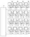
ひとつは、図1に示すように、複数のNANDコントローラ11a〜11dと、それらNANDコントローラ11a〜11dを束ねる親回路12によって、ツリー構成となるように並列化する構成である。In order to solve this problem, the following two configurations are conceivable.
One is a configuration in which a plurality of
図1に示す例では、NANDコントローラ11aは、メモリチップ13a〜13dが接続され、NANDコントローラ11bは、メモリチップ13e〜13hが接続され、NANDコントローラ11cは、メモリチップ13i〜13lが接続され、NANDコントローラ11dは、メモリチップ13m〜13pが接続されている。 In the example shown in FIG. 1, the
もうひとつは、図2に示すように、NANDコントローラ21の入出力ピンを複数のメモリチップ22a〜22pでバス共有する構成である。 The other is a configuration in which the input / output pins of the NAND controller 21 are shared by a plurality of
前者のツリー構成は、複数のNANDコントローラ11a〜11dと、親回路12が必要となるため、実装面積が増大し、小型化の面で不利である。
後者のバス共有は、単独のNANDコントローラ21によって多数のメモリチップ22a〜22pを制御できるため、実装面積の点から小型化に有利であるが、前者の構成よりも高速化の面で不利である。The former tree configuration requires a plurality of
The latter bus sharing is advantageous for downsizing from the viewpoint of mounting area because a large number of
そこで、本発明では、単一のNANDコントローラにバス共有で多数のメモリチップを制御し、かつ、書き込み速度の高速化を図るため、インタリーブ書き込み処理を採用する構成を提案する。なお、以下では、記録装置の一例としてNANDフラッシュメモリ記録装置の構成と動作について説明するが、これに限られない。 Therefore, the present invention proposes a configuration that employs interleaved write processing in order to control a large number of memory chips by sharing a bus with a single NAND controller and to increase the write speed. In the following, the configuration and operation of a NAND flash memory recording device will be described as an example of a recording device, but the present invention is not limited to this.
NANDフラッシュメモリ記録装置1は、図3に示すように、メモリチップ31と、コントローラ(制御部)32と、を備える。 As shown in FIG. 3, the NAND flash
メモリチップ31は、複数のメモリによって構成される。本実施例では、メモリチップ31は、4つのメモリ33a〜33dによって構成されている。また、メモリ33a〜33dは、シリコンダイとも呼ばれ、データレジスタとメモリセルアレイとにより構成されている。 The
コントローラ32は、メモリ33a〜33dにアクセスし、データの書き込み、読み出し及び消去を行う。コントローラ32は、メモリ33a〜33dのそれぞれを仮想的に所定の容量で分割したページ単位で管理する。 The
コントローラ32は、複数のメモリ33a〜33dに対して同一ページである第1ページを指定して、順次、データを転送し、データの転送を開始した最初のメモリの第1ページに対するデータの書き込みが完了している場合には、複数のメモリ33a〜33dに対して同一ページである第2ページを指定して、順次、データを転送することにより、複数のメモリ33a〜33dにデータを書き込んで行くインタリーブ書き込み処理を実行する。 The
詳細には、各メモリ33a〜33dにデータを転送すると、各メモリ33a〜33dのデータレジスタにデータが格納される。その後、データレジスタから、メモリセルアレイ(指定されたページ)にデータが書き込まれる。 Specifically, when data is transferred to the
一般的にNANDフラッシュメモリ記録装置は、ページによって、書き込み速度が高速なページと低速なページが存在する。
本実施例に係るNANDフラッシュメモリ記録装置1は、各メモリ33a〜33dの同一ページに対して、順次、データの転送と書き込みを実行するので、連続的なデータを書き込む場合に、書き込み速度が高速なページと書き込み速度が低速なページとを混在させずに、書き込み速度の足並みを揃えることができ、高速に高データレートの映像記録に対応することができる。In general, a NAND flash memory recording device includes a page with a high writing speed and a page with a low speed depending on the page.
Since the NAND flash
メモリチップ31は、多数並列化して構成されてもよい。
かかる構成によれば、NANDフラッシュメモリ記録装置1は、複数のメモリチップ31の各メモリの同一ページに対して、順次、データの転送と書き込みを実行するので、連続的なデータを書き込む場合に、書き込み速度が高速なページと書き込み速度が低速なページとを混在させずに、書き込み速度の足並みを揃えることができ、高速に高データレートの映像記録に対応することができる。
According to such a configuration, the NAND flash
ここで、一般的にインタリーブ書き込み処理による高速化は、ひとつのメモリチップの内部に備えられる複数(2〜4個)のシリコンダイ(メモリ)に対して適用されるが、二つ以上の複数のメモリチップに対しても同様に適用可能である。
例えば、4枚のメモリチップに対してインタリーブ書き込み処理を適用する場合は、8〜16個のシリコンダイに対して書き込み制御を行うことになる。Here, generally, the speeding up by the interleave writing process is applied to a plurality (2 to 4) of silicon dies (memory) provided in one memory chip. The same applies to memory chips.
For example, when the interleave writing process is applied to four memory chips, writing control is performed on 8 to 16 silicon dies.
また、上述したように、MLC型NANDフラッシュメモリ記録装置には、ページによって、書き込みが高速なページと低速なページが存在する。
一例として、容量256GbitのMLC型NANDフラッシュメモリ記録装置の各ページに複数回記録を行い、記録速度の計測結果を重ねてプロットした結果を図4に示す。
図4から分かるように、書き込み時間が最大500μsec程度の高速ページ(0,1,4,5,8,9・・・)と、書き込み時間が最大1900μsec程度の低速ページ(2,6,10・・・)と、書き込み時間が最大1500μsec程度の中速ページ(3,7,11・・・)の三種類が存在する。Further, as described above, in the MLC NAND flash memory recording apparatus, there are pages that are written at high speed and pages that are written at low speed depending on the page.
As an example, FIG. 4 shows a result obtained by performing recording a plurality of times on each page of an MLC NAND flash memory recording apparatus having a capacity of 256 Gbit and plotting the recording speed measurement results.
As can be seen from FIG. 4, a high-speed page (0, 1, 4, 5, 8, 9...) With a maximum write time of about 500 μsec and a low-speed page with a maximum write time of about 1900 μsec (2, 6, 10,. ..) And medium speed pages (3, 7, 11...) Having a maximum write time of about 1500 μsec.
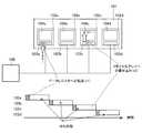
ここで、コントローラ32により高速ページ、中速ページ及び低速ページの書き込み順番を制御し、インタリーブ書き込み速度の最適化を図る処理について以下に説明する。なお、以下では、NANDフラッシュメモリ記録装置1は、図5(a)に示すように、4枚のメモリチップ31a〜31dを備えるものとする。また、メモリチップ31aは、4個のメモリ33a〜33dを備え、メモリチップ31bは、同様に4個のメモリ33e〜33hを備え、メモリチップ31cは、同様に4個のメモリ33i〜33lを備え、メモリチップ31dは、同様に4個のメモリ33m〜33pを備える。 Here, a process for controlling the writing order of the high-speed page, the medium-speed page, and the low-speed page by the
また、図5(b)には、コントローラ32によって、高速ページ、中速ページ及び低速ページの書き込み順番を制御した一例を示している。
図5(b)では高速ページ、中速ページ、低速ページのそれぞれをまとめてインタリーブするよう書き込み順番を制御している。FIG. 5B shows an example in which the
In FIG. 5B, the write order is controlled so that high-speed pages, medium-speed pages, and low-speed pages are interleaved together.
具体的には、コントローラ32は、メモリチップ31aのメモリ33aの第0ページ(高速ページ)にデータを転送し、転送終了後、メモリチップ31aのメモリ33bの第0ページにデータを転送し、転送終了後、メモリチップ31aのメモリ33cの第0ページにデータを転送する処理を、メモリチップ31dのメモリ33pの第0ページまで順次行う。 Specifically, the
コントローラ32は、メモリチップ31aのメモリ33aの第0ページに対するデータの書き込みが完了している場合には、メモリチップ31aのメモリ33aの第1ページ(高速ページ)にデータを転送し、当該処理をメモリチップ31dのメモリ33pの第1ページまで順次行う。 When the writing of data to the 0th page of the
図5(b)に示す例では、メモリチップ31dのメモリ33pの第3ページ(中速ページ)にデータを転送し、データを書き込むまでの様子を模式的に示しており、メモリチップ4枚(メモリ16個)の構成で、4ページをインタリーブ書き込みするのに要する時間は5100μsecになった。 In the example shown in FIG. 5B, a state from when data is transferred to the third page (medium speed page) of the
次に、本実施例のように各ページの書き込み速度に基づいて、ページの順番を制御しない、すなわち、書き込み速度が異なるページを混在させてインタリーブした場合の一例を図6に示す。 Next, FIG. 6 shows an example in which the page order is not controlled based on the writing speed of each page as in the present embodiment, that is, the pages are interleaved with different writing speeds.
図6に示す例では、メモリチップ31dのメモリ33oのページ(低速ページ)に対するデータの書き込みに時間がかかり、次のデータを同一のメモリ33oへ転送できない時間が発生しており(図6中のA)、さらに、メモリチップ31dのメモリ33oのページ(中速ページ)に対するデータの書き込みに時間がかかり、次のデータを同一のメモリ33oへ転送できない時間が発生している(図6中のB)。 In the example shown in FIG. 6, it takes time to write data to the page (low speed page) of the
よって、図6に示す例では、4ページをインタリーブ書き込みするのに要する時間は、5850μsecであり、書き込み速度が異なるページを混在させたことによる、書き込み速度の低下が確認できる。 Therefore, in the example shown in FIG. 6, the time required for interleaved writing of four pages is 5850 μsec, and it can be confirmed that the writing speed is lowered due to the mixing of pages having different writing speeds.
本実施例に係るNANDフラッシュメモリ記録装置1は、書き込み速度が同じページを一括してインタリーブすることで、書き込み時間の最適化を図ることができ、特に、連続したデータ(映像)記録に有効となる。 The NAND flash
上述では、それぞれ4個のメモリを有する4枚のメモリチップ31a〜31dを備える構成について説明したが、これに限られない。
例えば、NANDフラッシュメモリ記録装置1は、図7に示すように、4枚のメモリチップを8並列(メモリチップ31n1〜31n32)でコントローラ32にバス共有で接続する構成でもよい。In the above description, the configuration including four
For example, as shown in FIG. 7, the NAND flash
メモリチップ1枚当たりの容量は256Gbit、チップ1枚あたりの入出力ピン数は50本である。NANDフラッシュメモリ記録装置1の接続に使用される入出力ピンの総数は、1600本となる。従来の構成では、メモリチップ32枚を並列接続した場合の6400本となる。 The capacity per memory chip is 256 Gbit, and the number of input / output pins per chip is 50. The total number of input / output pins used for connection of the NAND flash
本実施例を適用した場合、32枚のメモリチップを並列接続しても、入出力ピンの総数が従来の構成に比して、1/4の本数で済むことになる。
よって、NANDフラッシュメモリ記録装置1は、一つのコントローラで32枚のメモリチップに対して、インタリーブ書き込み処理を実行することができる。When this embodiment is applied, even if 32 memory chips are connected in parallel, the total number of input / output pins is ¼ that of the conventional configuration.
Therefore, the NAND flash
また、インタリーブするダイ(メモリ)の個数と書込み速度の理論値の関係を図8に示す。
一般的なSSDの構成に相当する8枚のメモリチップを並列接続した場合、3.4Gbpsであるのに対して、本実施例を適用した構成では、9.8Gbps以上の書込み速度を見込むことができる。このようにして、NANDフラッシュメモリ記録装置1は、バス共有の構成でも高速化を図ることが可能なことが分かる。FIG. 8 shows the relationship between the number of dies (memory) to be interleaved and the theoretical value of the writing speed.
When eight memory chips corresponding to a general SSD configuration are connected in parallel, the speed is 3.4 Gbps, whereas in the configuration to which this embodiment is applied, a writing speed of 9.8 Gbps or more can be expected. it can. In this way, it can be seen that the NAND flash
上述したように、本実施例に係るNANDフラッシュメモリ記録装置1は、一つのコントローラ32によって多数のメモリチップへの書込み制御が可能となり、実装面積の増大を抑えて小型で大容量な記録媒体を実現するとともに、インタリーブ書き込み処理の最適化により高データレート映像の記録に対応することができる。 As described above, the NAND flash
また、本実施例では、主に記録装置の構成と動作について説明したが、これに限られず、各構成要素を備え、メモリチップの並列化数を増大させずに、高データレート映像の記録に対応するための記録方法、及びプログラムとして構成されてもよい。 In the present embodiment, the configuration and operation of the recording apparatus have been mainly described. However, the present invention is not limited to this, and each component is provided for recording a high data rate video without increasing the number of parallel memory chips. It may be configured as a recording method and program for responding.
さらに、記録装置の機能を実現するためのプログラムをコンピュータで読み取り可能な記録媒体に記録して、この記録媒体に記録されたプログラムをコンピュータシステムに読み込ませ、実行することによって実現してもよい。 Furthermore, the program for realizing the function of the recording apparatus may be recorded on a computer-readable recording medium, and the program recorded on the recording medium may be read by a computer system and executed.
ここでいう「コンピュータシステム」とは、OSや周辺機器等のハードウェアを含むものとする。また、「コンピュータで読み取り可能な記録媒体」とは、フレキシブルディスク、光磁気ディスク、ROM、CD−ROM等の可搬媒体、コンピュータシステムに内蔵されるハードディスク等の記録装置のことをいう。 The “computer system” here includes an OS and hardware such as peripheral devices. The “computer-readable recording medium” refers to a recording device such as a portable medium such as a flexible disk, a magneto-optical disk, a ROM, a CD-ROM, or a hard disk built in a computer system.
さらに「コンピュータで読み取り可能な記録媒体」とは、インターネット等のネットワークや電話回線等の通信回線を介してプログラムを送信する場合の通信線のように、短時刻の間、動的にプログラムを保持するもの、その場合のサーバやクライアントとなるコンピュータシステム内部の揮発性メモリのように、一定時刻プログラムを保持しているものも含んでもよい。また、上記プログラムは、前述した機能の一部を実現するためのものであってもよく、さらに前述した機能をコンピュータシステムにすでに記録されているプログラムとの組み合わせで実現できるものであってもよい。 Furthermore, “computer-readable recording medium” means that a program is dynamically held for a short time, like a communication line when transmitting a program via a network such as the Internet or a communication line such as a telephone line. It is also possible to include one that holds a program for a certain time, such as a volatile memory inside a computer system that becomes a server or client in that case. Further, the program may be for realizing a part of the above-described functions, and may be capable of realizing the above-described functions in combination with a program already recorded in the computer system. .
1 NANDフラッシュメモリ記録装置
31 メモリチップ
32 コントローラ
31a〜31d メモリチップDESCRIPTION OF
Claims (3)
Translated fromJapanese前記メモリにアクセスし、データの書き込み、読み出し及び消去を行う制御部と、を備え、
前記制御部は、前記メモリのそれぞれを仮想的に所定の容量で分割したページ単位で管理し、
前記複数のメモリに対して同一ページである第1ページを指定して、順次、データを転送し、データの転送を開始した最初のメモリの前記第1ページに対するデータの書き込みが完了している場合には、前記複数のメモリに対して同一ページである第2ページを指定して、順次、データを転送することにより、前記複数のメモリにデータを書き込んで行くインタリーブ書き込み処理を実行する記録装置。A memory chip composed of a plurality of memories;
A controller that accesses the memory and writes, reads, and erases data;
The control unit manages each of the memories in units of pages virtually divided by a predetermined capacity,
When the first page, which is the same page, is specified for the plurality of memories, the data is sequentially transferred, and the data writing to the first page of the first memory that has started the data transfer is completed A recording device that executes an interleaved writing process of writing data to the plurality of memories by designating a second page that is the same page as the plurality of memories and sequentially transferring the data.
前記制御工程では、前記メモリのそれぞれを仮想的に所定の容量で分割したページ単位で管理し、
前記複数のメモリに対して同一ページである第1ページを指定して、順次、データを転送し、データの転送を開始した最初のメモリの前記第1ページに対するデータの書き込みが完了している場合には、前記複数のメモリに対して同一ページである第2ページを指定して、順次、データを転送することにより、前記複数のメモリにデータを書き込んで行くインタリーブ書き込み処理を実行する記録方法。A control step of accessing a memory chip composed of a plurality of memories and writing, reading and erasing data;
In the control step, each of the memories is managed in units of pages virtually divided by a predetermined capacity,
When the first page, which is the same page, is specified for the plurality of memories, the data is sequentially transferred, and the data writing to the first page of the first memory that has started the data transfer is completed In the recording method, the second page which is the same page is designated for the plurality of memories, and the data is sequentially transferred to perform an interleaved writing process for writing the data to the plurality of memories.
Priority Applications (1)
| Application Number | Priority Date | Filing Date | Title |
|---|---|---|---|
| JP2012253041AJP2014102610A (en) | 2012-11-19 | 2012-11-19 | Recording apparatus, and recording method |
Applications Claiming Priority (1)
| Application Number | Priority Date | Filing Date | Title |
|---|---|---|---|
| JP2012253041AJP2014102610A (en) | 2012-11-19 | 2012-11-19 | Recording apparatus, and recording method |
Publications (1)
| Publication Number | Publication Date |
|---|---|
| JP2014102610Atrue JP2014102610A (en) | 2014-06-05 |
Family
ID=51025080
Family Applications (1)
| Application Number | Title | Priority Date | Filing Date |
|---|---|---|---|
| JP2012253041APendingJP2014102610A (en) | 2012-11-19 | 2012-11-19 | Recording apparatus, and recording method |
Country Status (1)
| Country | Link |
|---|---|
| JP (1) | JP2014102610A (en) |
Cited By (1)
| Publication number | Priority date | Publication date | Assignee | Title |
|---|---|---|---|---|
| JP2022042183A (en)* | 2020-09-02 | 2022-03-14 | 株式会社東芝 | Memory device, video server, broadcasting system, and memory access control method |
Citations (3)
| Publication number | Priority date | Publication date | Assignee | Title |
|---|---|---|---|---|
| JP2010282492A (en)* | 2009-06-05 | 2010-12-16 | Toshiba Corp | Memory system |
| JP2010287303A (en)* | 2009-05-15 | 2010-12-24 | Panasonic Corp | Semiconductor recording device |
| WO2012030388A2 (en)* | 2010-08-31 | 2012-03-08 | Micron Technology, Inc. | Stripe-based non-volatile multilevel memory operation |
- 2012
- 2012-11-19JPJP2012253041Apatent/JP2014102610A/enactivePending
Patent Citations (3)
| Publication number | Priority date | Publication date | Assignee | Title |
|---|---|---|---|---|
| JP2010287303A (en)* | 2009-05-15 | 2010-12-24 | Panasonic Corp | Semiconductor recording device |
| JP2010282492A (en)* | 2009-06-05 | 2010-12-16 | Toshiba Corp | Memory system |
| WO2012030388A2 (en)* | 2010-08-31 | 2012-03-08 | Micron Technology, Inc. | Stripe-based non-volatile multilevel memory operation |
Cited By (1)
| Publication number | Priority date | Publication date | Assignee | Title |
|---|---|---|---|---|
| JP2022042183A (en)* | 2020-09-02 | 2022-03-14 | 株式会社東芝 | Memory device, video server, broadcasting system, and memory access control method |
Similar Documents
| Publication | Publication Date | Title |
|---|---|---|
| JP7736776B2 (en) | Scatter and gather streaming data with circular FIFO | |
| TW201423577A (en) | Mobile device and data management method using the same | |
| US11379155B2 (en) | System and method for flash storage management using multiple open page stripes | |
| JP5068300B2 (en) | Apparatus, method and program for data flow and memory sharing of processor | |
| US20180173460A1 (en) | Contention reduction scheduler for nand flash array with raid | |
| CN111679783A (en) | memory controller | |
| US20240152471A1 (en) | Data format conversion apparatus and method | |
| US10225425B2 (en) | Information processing apparatus and method for controlling the same | |
| US20150378813A1 (en) | Semiconductor memory card, method for controlling the same, and semiconductor memory system | |
| US9256439B2 (en) | Parallel processing of two-dimensional data, storage of plural data of the processing results in a cache line and transfer of the data to a memory as in the cache line | |
| WO2024074012A1 (en) | Video transmission control method, apparatus and device, and nonvolatile readable storage medium | |
| US8392630B2 (en) | Information processing apparatus having first DMA controller and second DMA controller wherein selection circuit determines which DMA will perform data transfer based on higher data transfer performance | |
| US7916975B2 (en) | Image processing apparatus and image processing control method | |
| JP7403457B2 (en) | Near-memory hardened compute blocks for configurable computing boards | |
| JP2012234458A (en) | Image processing device, and control method and program for image processing device | |
| JP2014102610A (en) | Recording apparatus, and recording method | |
| CN109246363B (en) | A DMD system and its access method | |
| US8688947B1 (en) | Aligned data access | |
| US8285932B2 (en) | Mass storage system with improved usage of buffer capacity | |
| WO2018084004A1 (en) | Device controller, device, control method, program, and device control system | |
| US20120159024A1 (en) | Semiconductor apparatus | |
| US11928364B2 (en) | Memory system and method | |
| CN101018327B (en) | Discrete Cosine Transform Integrated Module and Operation Combination Method | |
| JP2011013736A (en) | Nonvolatile memory device and nonvolatile memory controller | |
| WO2022011614A1 (en) | Dma controller, electronic device, chip, mobile platform and data migration method |
Legal Events
| Date | Code | Title | Description |
|---|---|---|---|
| A621 | Written request for application examination | Free format text:JAPANESE INTERMEDIATE CODE: A621 Effective date:20151001 | |
| A977 | Report on retrieval | Free format text:JAPANESE INTERMEDIATE CODE: A971007 Effective date:20160721 | |
| A131 | Notification of reasons for refusal | Free format text:JAPANESE INTERMEDIATE CODE: A131 Effective date:20160726 | |
| A02 | Decision of refusal | Free format text:JAPANESE INTERMEDIATE CODE: A02 Effective date:20170207 |