JP2014093463A - Surface emitting semiconductor laser array device, light source and light source module - Google Patents
Surface emitting semiconductor laser array device, light source and light source moduleDownload PDFInfo
- Publication number
- JP2014093463A JP2014093463AJP2012244089AJP2012244089AJP2014093463AJP 2014093463 AJP2014093463 AJP 2014093463AJP 2012244089 AJP2012244089 AJP 2012244089AJP 2012244089 AJP2012244089 AJP 2012244089AJP 2014093463 AJP2014093463 AJP 2014093463A
- Authority
- JP
- Japan
- Prior art keywords
- semiconductor laser
- array device
- laser array
- type semiconductor
- metal wiring
- Prior art date
- Legal status (The legal status is an assumption and is not a legal conclusion. Google has not performed a legal analysis and makes no representation as to the accuracy of the status listed.)
- Granted
Links
- 239000004065semiconductorSubstances0.000titleclaimsabstractdescription125
- 239000002184metalSubstances0.000claimsabstractdescription107
- 229910052751metalInorganic materials0.000claimsabstractdescription107
- 239000000758substrateSubstances0.000claimsabstractdescription62
- 239000011159matrix materialSubstances0.000claimsabstractdescription5
- 239000000463materialSubstances0.000claimsdescription8
- 230000010355oscillationEffects0.000claimsdescription7
- 230000017525heat dissipationEffects0.000claimsdescription5
- 150000002739metalsChemical class0.000abstract2
- 239000010410layerSubstances0.000description44
- 229910001218Gallium arsenideInorganic materials0.000description24
- 229910000679solderInorganic materials0.000description8
- 238000001816coolingMethods0.000description7
- 238000000926separation methodMethods0.000description7
- 238000005530etchingMethods0.000description6
- 239000011229interlayerSubstances0.000description6
- 230000020169heat generationEffects0.000description5
- 230000031700light absorptionEffects0.000description5
- 238000004519manufacturing processMethods0.000description5
- 239000012535impuritySubstances0.000description4
- 229910000980Aluminium gallium arsenideInorganic materials0.000description3
- 238000002955isolationMethods0.000description3
- 238000005498polishingMethods0.000description3
- 230000015572biosynthetic processEffects0.000description2
- 239000010949copperSubstances0.000description2
- 230000006378damageEffects0.000description2
- 238000010586diagramMethods0.000description2
- 238000000034methodMethods0.000description2
- 239000000203mixtureSubstances0.000description2
- RYGMFSIKBFXOCR-UHFFFAOYSA-NCopperChemical compound[Cu]RYGMFSIKBFXOCR-UHFFFAOYSA-N0.000description1
- 229910000530Gallium indium arsenideInorganic materials0.000description1
- 238000010521absorption reactionMethods0.000description1
- 150000001875compoundsChemical class0.000description1
- 229910052802copperInorganic materials0.000description1
- 230000007547defectEffects0.000description1
- 229910052737goldInorganic materials0.000description1
- 230000012447hatchingEffects0.000description1
- 239000011810insulating materialSubstances0.000description1
- 239000007769metal materialSubstances0.000description1
- 238000002488metal-organic chemical vapour depositionMethods0.000description1
- 238000012986modificationMethods0.000description1
- 230000004048modificationEffects0.000description1
- 230000003647oxidationEffects0.000description1
- 238000007254oxidation reactionMethods0.000description1
- 238000000206photolithographyMethods0.000description1
- 229920001721polyimidePolymers0.000description1
- 239000009719polyimide resinSubstances0.000description1
- 239000003507refrigerantSubstances0.000description1
- 229910052814silicon oxideInorganic materials0.000description1
- 125000006850spacer groupChemical group0.000description1
- XLYOFNOQVPJJNP-UHFFFAOYSA-NwaterSubstancesOXLYOFNOQVPJJNP-UHFFFAOYSA-N0.000description1
Images


Landscapes
- Semiconductor Lasers (AREA)
Abstract
Description
Translated fromJapanese本発明は、面発光型半導体レーザアレイ装置、光源および光源モジュールに関する。 The present invention relates to a surface emitting semiconductor laser array device, a light source, and a light source module.
近年、医療・工業の分野で高出力半導体レーザが求められている。一般的に、高出力半導体レーザでは、端面出射レーザが使用されるが、端面出射レーザでは端面破壊が発生し、素子特性が悪くなりやすい。他方、面発光型半導体レーザは、端面破壊を起こさない半導体レーザとして注目されており、温度上昇に対する許容が端面出射レーザに比べ優れている。面発光型半導体レーザを使用して高出力半導体レーザを作製するには、大規模なアレイ構造を作製する必要がある。面発光型半導体レーザ素子を直列接続し、一部の面発光型半導体レーザ素子が故障しても他の面発光型半導体レーザ素子で発光を継続させることができる長寿命の面発光型半導体レーザアレイが提案されている(特許文献1)。 In recent years, there has been a demand for high-power semiconductor lasers in the medical and industrial fields. In general, an edge emitting laser is used in a high-power semiconductor laser, but the edge emitting laser causes end face destruction, and the device characteristics tend to deteriorate. On the other hand, surface-emitting semiconductor lasers are attracting attention as semiconductor lasers that do not cause end face destruction, and allowance for temperature rise is superior to end face emission lasers. In order to produce a high-power semiconductor laser using a surface emitting semiconductor laser, it is necessary to produce a large-scale array structure. Long-lived surface emitting semiconductor laser array in which surface emitting semiconductor laser elements are connected in series, and even if some surface emitting semiconductor laser elements fail, other surface emitting semiconductor laser elements can continue to emit light Has been proposed (Patent Document 1).
本発明は、高密度化および高寿命化を図ることができる面発光型半導体レーザアレイ装置、光源および光源モジュールを提供することを目的とする。 An object of the present invention is to provide a surface emitting semiconductor laser array device, a light source, and a light source module that can achieve high density and long life.
請求項1は、第1の主面、当該第1の主面に対向する第2の主面を有する基板と、前記基板の第1の主面上に行列状に配された複数の面発光型半導体レーザ素子と、前記基板の第1の主面上に形成され、第1の列に配された複数の面発光型半導体レーザ素子の第1の電極に並列に電気的接続された第1の電極領域と、前記基板の第1の主面上に形成され、第2の列に配された複数の面発光型半導体レーザ素子の第2の電極に並列に電気的接続された第2の電極領域と、前記第1の電極領域と前記第2の電極領域との間に配された少なくとも1つの金属配線とを有し、前記金属配線は、一方の列と他方の列の間を列方向に延在する部分を含み、かつ一方の列の複数の面発光型半導体レーザ素子の第1の電極にそれぞれ電気的に接続された第1の接続部と、他方の列の複数の面発光型半導体レーザ素子の第2の電極にそれぞれ電気的に接続された第2の接続部とを有する、面発光型半導体レーザアレイ装置。
請求項2は、前記第1の接続部は、前記列方向に延在する部分から第1の行方向に延び、前記第2の接続部は、前記列方向に延在する部分から第1の行方向と反対の第2の行方向に延びる、請求項1に記載の面発光型半導体レーザアレイ装置。
請求項3は、前記第1の接続部は、前記第1の行方向に延在する複数の櫛形部を有し、前記第2の接続部は、前記第1の接続部の櫛形部と異なる位置で前記第2の行方向に延在する複数の櫛形部を有し、前記第1の接続部の櫛形部の各々は、一方の列の複数の面発光型半導体レーザ素子の各々の間を延在する、請求項1または2に記載の面発光型半導体レーザアレイ装置。
請求項4は、各面発光型半導体レーザ素子は、それぞれ柱状構造を有し、1つの柱状構造は、前記第1の接続部の一対の櫛形部の間に位置する、請求項3に記載の面発光型半導体レーザアレイ装置。
請求項5は、前記第2の接続部の櫛形部の各々は、他方の列の柱状構造の頂部において面発光型半導体レーザ素子に電気的に接続される、請求項4に記載の面発光型半導体レーザアレイ装置。
請求項6は、前記第1の接続部の櫛形部の各々は、一方の列の柱状構造の底部において面発光型半導体レーザ素子に電気的に接続される、請求項4に記載の面発光型半導体レーザアレイ装置。
請求項7は、前記基板は、半絶縁性でありかつ面発光型半導体レーザ素子の発振波長を透過可能な材料から構成され、複数の面発光型半導体レーザ素子のレーザ光は、前記基板の第2の主面から出射される、請求項1ないし6いずれか1つに記載の面発光型半導体レーザアレイ装置。
請求項8は、複数の面発光型半導体レーザ素子のレーザ光は、前記柱状構造の頂部から出射される、請求項1ないし6いずれか1つに記載の面発光型半導体レーザアレイ装置。
請求項9は、前記基板の第1の主面上に互いに電気的に分離された複数の島領域が形成され、各島領域には、列方向に配された複数の面発光型半導体レーザ素子が形成され、各島領域には、複数の面発光型半導体レーザ素子の第1の電極に共通の導電層が形成される、請求項1ないし8いずれか1つに記載の面発光型半導体レーザアレイ装置。
請求項10は、各島領域には、前記共通の導電層と前記第1の接続部とを接続するための接続孔が形成される、請求項9に記載の面発光型半導体レーザアレイ装置。
請求項11は、前記接続孔は、列方向に配列された柱状構造の間に形成される、請求項10に記載の面発光型半導体レーザアレイ装置。
請求項12は、前記接続孔は、列方向に配列された各柱状構造を取り囲むように形成される、請求項10に記載の面発光型半導体レーザアレイ装置。
請求項13は、前記接続孔は、前記島領域の列方向に沿って形成される、請求項10に記載の面発光型半導体レーザアレイ装置。
請求項14は、前記基板は、半絶縁性の半導体材料から構成され、前記島領域は、前記共通の導電層に前記基板に到達する溝を形成することで形成される、請求項9に記載の面発光型半導体レーザアレイ装置。
請求項15は、前記第1の電極領域は、アノード側電極パッドであり、前記第2の電極領域は、カソード側電極パッドであり、前記アノード側電極パッドおよび前記カソード側電極パッドは、前記基板の両端部に配され、前記アノード側電極パッドおよび前記カソード側電極パッドの列方向の長さは、列方向の複数の面発光型半導体レーザ素子の全体の間隔と等しいかまたはそれより大きい、請求項1に記載の面発光型半導体レーザアレイ装置。
請求項16は、請求項1ないし15いずれか1つに記載の面発光型半導体レーザアレイ装置と、前記面発光型半導体レーザアレイ装置を駆動する駆動手段と、前記面発光型半導体レーザアレイ装置に熱的に結合され、前記面発光型半導体レーザアレイ装置で発生された熱を放熱させる放熱手段と、を有する光源。
請求項17は、請求項1ないし15いずれか1つに記載の複数の面発光型半導体レーザアレイ装置と、複数の面発光型半導体レーザアレイ装置の配列方向と並行に延在するアノード側の金属配線、カソード側の金属配線、および放熱用の金属配線とを含み、前記アノード側の金属配線は、複数の面発光型半導体レーザアレイ装置のアノード側電極パッドに共通に電気的に接続され、前記カソード側の金属配線は、複数の面発光型半導体レーザアレイ装置のカソード側電極パッドに共通に電気的に接続され、前記放熱用の金属配線は、前記アノード側の金属配線と前記カソード側の金属配線の間に配列される、光源モジュール。
請求項18は、複数の面発光型半導体レーザアレイ装置のアノード側電極パッドおよびカソード側電極パッドは、前記アノード側の金属配線および前記カソード側の金属配線に表面実装される、請求項17に記載の光源モジュール。
According to a second aspect of the present invention, the first connection portion extends from the portion extending in the column direction in the first row direction, and the second connection portion is formed from the portion extending in the column direction. 2. The surface-emitting type semiconductor laser array device according to
According to a third aspect of the present invention, the first connecting portion has a plurality of comb-shaped portions extending in the first row direction, and the second connecting portion is different from the comb-shaped portion of the first connecting portion. A plurality of comb-shaped portions extending in the second row direction at positions, and each of the comb-shaped portions of the first connection portion is between each of the plurality of surface-emitting type semiconductor laser elements in one column. The surface-emitting type semiconductor laser array device according to
According to a fourth aspect of the present invention, each of the surface-emitting type semiconductor laser elements has a columnar structure, and one columnar structure is located between a pair of comb-shaped portions of the first connection portion. Surface emitting semiconductor laser array device.
5. The surface-emitting type according to claim 4, wherein each of the comb-shaped portions of the second connection portion is electrically connected to the surface-emitting type semiconductor laser element at the top of the columnar structure in the other row. Semiconductor laser array device.
6. The surface-emitting type according to claim 4, wherein each of the comb-shaped portions of the first connection portion is electrically connected to the surface-emitting type semiconductor laser element at the bottom of the columnar structure in one row. Semiconductor laser array device.
According to a seventh aspect of the present invention, the substrate is made of a material that is semi-insulating and capable of transmitting the oscillation wavelength of the surface-emitting type semiconductor laser device, and the laser light of the plurality of surface-emitting type semiconductor laser devices is emitted from the substrate. The surface emitting semiconductor laser array device according to
8. The surface-emitting type semiconductor laser array device according to
A plurality of island regions electrically isolated from each other are formed on the first main surface of the substrate, and a plurality of surface-emitting type semiconductor laser elements arranged in the column direction in each island region The surface emitting semiconductor laser according to
10. The surface emitting semiconductor laser array device according to claim 9, wherein a connection hole for connecting the common conductive layer and the first connection portion is formed in each island region.
11. The surface emitting semiconductor laser array device according to
12. The surface emitting semiconductor laser array device according to
13. The surface emitting semiconductor laser array device according to
14. The substrate according to claim 9, wherein the substrate is made of a semi-insulating semiconductor material, and the island region is formed by forming a groove reaching the substrate in the common conductive layer. Surface emitting semiconductor laser array device.
The fifteenth aspect is that the first electrode region is an anode side electrode pad, the second electrode region is a cathode side electrode pad, and the anode side electrode pad and the cathode side electrode pad are the substrate. The length in the column direction of the anode side electrode pad and the cathode side electrode pad is equal to or larger than the entire interval of the plurality of surface emitting semiconductor laser elements in the column direction.
A sixteenth aspect of the present invention provides a surface emitting semiconductor laser array device according to any one of the first to fifteenth aspects, a driving unit that drives the surface emitting semiconductor laser array device, and the surface emitting semiconductor laser array device. A heat source that is thermally coupled to dissipate heat generated by the surface-emitting type semiconductor laser array device.
According to a seventeenth aspect of the present invention, there is provided a plurality of surface-emitting type semiconductor laser array devices according to any one of the first to fifteenth aspects and an anode-side metal extending in parallel with the arrangement direction of the plurality of surface-emitting type semiconductor laser array devices. The anode side metal wiring is electrically connected in common to the anode side electrode pads of the plurality of surface emitting semiconductor laser array devices, The metal wiring on the cathode side is electrically connected in common to the cathode side electrode pads of the plurality of surface emitting semiconductor laser array devices, and the metal wiring for heat dissipation includes the metal wiring on the anode side and the metal on the cathode side. A light source module arranged between wirings.
18. The anode-side electrode pad and the cathode-side electrode pad of the plurality of surface-emitting type semiconductor laser array devices are surface-mounted on the anode-side metal wiring and the cathode-side metal wiring, respectively. Light source module.
請求項1によれば、金属配線を持たない従来の面発光型半導体レーザアレイ装置と比較して、配線の高寿命化および素子の高密度化を図ることができる。
請求項2、3によれば、第1および第2の接続部を持たない構成と比較して、アレイ装置の発熱を低減することができる。
請求項4、5、6によれば、柱状構造で発生した熱を効果的に放熱させることができる。
請求項7、8によれば、基板を薄型化するための工程を省略することができる。
請求項9、10によれば、面発光型半導体レーザ素子の第1の電極との接続を容易にすることができる。
請求項11、12、13によれば、第1の接続部と共通の導電層との間の接触抵抗を低減することができる。
請求項14によれば、島領域の形成を容易にすることができる。
請求項15によれば、発熱の低減を図ることができる。According to the first aspect, compared to a conventional surface emitting semiconductor laser array device having no metal wiring, the life of the wiring and the density of the elements can be increased.
According to the second and third aspects, the heat generation of the array device can be reduced as compared with the configuration having no first and second connection portions.
According to the fourth, fifth, and sixth aspects, the heat generated in the columnar structure can be effectively dissipated.
According to the seventh and eighth aspects, the process for thinning the substrate can be omitted.
According to the ninth and tenth aspects, the connection with the first electrode of the surface emitting semiconductor laser element can be facilitated.
According to the eleventh, twelfth and thirteenth aspects, the contact resistance between the first connecting portion and the common conductive layer can be reduced.
According to the fourteenth aspect, the formation of the island region can be facilitated.
According to the fifteenth aspect, heat generation can be reduced.
本発明の好ましい実施形態を図面を参照して説明する。以下の説明では、酸化狭窄構造の面発光型半導体レーザを例示し、面発光型半導体レーザをVCSEL(Vertical Cavity Surface Emitting Laser)と称する。なお、図面のスケールは、発明の特徴を分かり易くするために強調しており、必ずしも実際のデバイスのスケールと同一ではないことに留意すべきである。 A preferred embodiment of the present invention will be described with reference to the drawings. In the following description, a surface emitting semiconductor laser having an oxide confinement structure is exemplified, and the surface emitting semiconductor laser is referred to as a VCSEL (Vertical Cavity Surface Emitting Laser). It should be noted that the scale of the drawings is emphasized for easy understanding of the features of the invention and is not necessarily the same as the scale of an actual device.
発振光を透過する導電性基板上にVCSELアレイを形成し、基板のキャリア濃度に依存した光吸収を低減させるように基板の厚さを薄く(例えば、200mm以下)研磨した後、裏面出射用の開口部を持つ裏面電極を形成し、VCSELアレイを反転して実装することで、発熱を抑制した大電流同時駆動の高出力VCSELアレイが考案されている。 A VCSEL array is formed on a conductive substrate that transmits oscillation light, and the substrate is thinly polished (for example, 200 mm or less) so as to reduce light absorption depending on the carrier concentration of the substrate. A high-power VCSEL array that simultaneously drives a large current and suppresses heat generation has been devised by forming a back electrode having an opening and mounting the VCSEL array by inverting it.
この種のVCSELアレイは、基板研磨後の加工工程が複雑となり、また、大電流駆動されるチップをレーザバー上に並べる場合、多数のワイヤボンディングを必要とするため、チップを高密度化することが難しく、かつ、1チップにオープンのような不具合が生じるとレーザバー全体が発光しなくなるという不具合がある。 In this type of VCSEL array, the processing steps after polishing the substrate are complicated, and when a chip driven by a large current is arranged on the laser bar, a large number of wire bondings are required. It is difficult, and there is a problem that the entire laser bar does not emit light when a problem such as opening occurs in one chip.
本発明の好ましい1つの実施態様では、半絶縁性(SI:Semi Insulating)の基板を用いてVCSELアレイを構成することで、裏面出射時の基板による光吸収を低減する。基板による吸収の影響が抑制されるため、従来のように基板を薄型化するような研磨が不要となり、製造工程の容易化を図る。また、チップ上の配線に流れる電流を低減した低電流駆動アレイチップを構成することより、発熱を低減し、配線の寿命を改善する。さらに、チップの両端に電流電圧印加用の電極パッドを形成することで、レーザバーにおけるチップの高密度化を図る。 In a preferred embodiment of the present invention, the VCSEL array is configured using a semi-insulating (SI) substrate, thereby reducing light absorption by the substrate during backside emission. Since the influence of absorption by the substrate is suppressed, polishing for thinning the substrate as in the prior art is unnecessary, and the manufacturing process is facilitated. Further, by constructing a low current drive array chip in which the current flowing through the wiring on the chip is reduced, heat generation is reduced and the life of the wiring is improved. Further, by forming electrode pads for applying a current voltage at both ends of the chip, the density of the chip in the laser bar is increased.
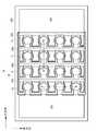
図1は、本発明の第1の実施例に係る面発光型半導体レーザアレイ装置の概略平面図、図2は、図1の表面から金属配線を取り除いた状態を示す平面図、図3(A)は、図1のA−A線断面図、図3(B)は、図1のB−B線断面図である。また、図4(A)は、アノード側の電極パッドの平面図、図4(B)は、島領域に形成されたVCSEL素子を直並列接続するための金属配線の平面図、図4(C)は、カソード側の金属パッドの平面図、図5は、図1のVCSELアレイの等価回路図である。 1 is a schematic plan view of a surface-emitting type semiconductor laser array device according to a first embodiment of the present invention, FIG. 2 is a plan view showing a state in which metal wiring is removed from the surface of FIG. 1, and FIG. ) Is a cross-sectional view taken along line AA in FIG. 1, and FIG. 3B is a cross-sectional view taken along line BB in FIG. 4A is a plan view of the electrode pad on the anode side, FIG. 4B is a plan view of metal wiring for series-parallel connection of VCSEL elements formed in the island region, and FIG. ) Is a plan view of the metal pad on the cathode side, and FIG. 5 is an equivalent circuit diagram of the VCSEL array of FIG.
図2に示すように、基板100上には複数の島領域Sが形成される。1つの島領域Sは、列方向に延び、この島領域Sが行方向に複数配列されている。図の例では、4つの島領域Sが行方向に表されている。好ましい態様では、基板100は、半絶縁性(真正)のGaAs基板から構成され、基板100上には、図3に示すように、n型のGaAs層102をはじめ、多数の半導体層が形成されている。これらの半導体層は、エピタキシャル成長により形成される。島領域Sは、n型のGaAs層102に基板100に到達する深さの分離溝104を形成することで形成される。図2の例では、4つの矩形状の分離溝104により4つの島領域Sが形成されている。分離溝104は、基板に到達する深さであるため、1つの島領域Sは、隣接する島領域Sから分離され、互いに電気的に絶縁される。 As shown in FIG. 2, a plurality of island regions S are formed on the
1つの島領域Sには、列方向に整列された複数の円筒状のポスト(メサまたは柱状構造)Pが形成される。1つのポストPは、1つのVCSEL素子を規定する。図の例では、1つの島領域Sに、列方向に4つのポストPまたはVCSEL素子が形成されている。1つの島領域Sに形成されたn型のGaAs層102は、4つのVCSEL素子に共通のn側電極となる。 In one island region S, a plurality of cylindrical posts (mesa or columnar structures) P aligned in the column direction are formed. One post P defines one VCSEL element. In the example of the figure, four post P or VCSEL elements are formed in one island region S in the column direction. The n-
また、図2には、VCSEL素子のn側電極と電気的接続をとるためのコンタクトホールCnと、VCSEL素子のp側電極と電気的接続をとるためのコンタクトホールCpが示されている。図2に示す基板100の表面は、層間絶縁膜118(図3を参照)によって覆われており、層間絶縁膜118には、VCSEL素子のn側電極すなわちn型のGaAs層102と電気的接続をするためのコンタクトホールCnと、VCSEL素子のp側電極と接続するためのコンタクトホールCpとが形成される。コンタクトホールCnは、1つの島領域Sの列方向に整列されたポストPの間に形成される。コンタクトホールCnがポストPと対向する側面は、ポストPの円形に倣うような曲面を有し、コンタクトホールCnはできるだけポストPに隣接され、大きな面積のコンタクトホールCnが形成される。コンタクトホールCnは、上記したようにn型のGaAs層102を露出させ、後述するようにコンタクトホールCn内には、コンタクト用のn側金属122(図3を参照)が形成される。一方、コンタクトホールCpは、ポストPの頂部に形成され、コンタクトホールCpもできるだけ大きな面積で形成されることが望ましい。また、コンタクトホールCp内には、コンタクト用のp側金属120(図3を参照)が形成される。 FIG. 2 shows a contact hole Cn for electrical connection with the n-side electrode of the VCSEL element and a contact hole Cp for electrical connection with the p-side electrode of the VCSEL element. The surface of the
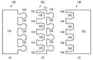
ここで図1を参照すると、図面の一番左側の島領域SAには、アノード側の電極パッド130が接続され、一番左側の島領域SCには、カソード側の電極パッド140が接続される。また、島領域SAと島領域SCの間の他の島領域S上には、中間の金属配線150が配され、これによりVCSEL素子が直並列接続される。Referring now to FIG. 1, the leftmost island region SA of the drawings, the
アノード側の電極パッド130は、基板100の一方の端部に配され、その列方向の長さは、1つの島領域Sの列方向の長さと等しいかそれいより幾分大きい。アノード側の電極パッド130は、図4(A)に示すように、外部との接続を行うための比較的大きな矩形状の面積を有する外部接続部132と、島領域SAの各VCSEL素子のp側電極と電気的接続するために行方向に櫛形状に延在する複数の円形状のフィンガ部134とを有する。ここでは、1つの島領域SAに形成されるVCSEL素子の数に合わせて4つの櫛形状のフィンガ部134が形成される。各フィンガ部134は、ポストPの頂部に形成されたコンタクトホールCpを介してVCSEL素子のp側金属120に電気的に接続される。こうして、一番左側の島領域SAの各VCSEL素子のp側金属120は、アノード側の電極パッド130に共通接続される。The anode-
カソード側の電極パッド140は、基板100の他方の端部に配され、その列方向の長さは、1つの島領域Sの列方向の長さと等しいかそれより幾分大きい。カソード側の電極パッド140は、図4(C)に示すように、外部との接続を行うための比較的大きな矩形状の面積を有する外部接続部142と、島領域SCの各VCSEL素子のn側金属122と電気的接続するために行方向に櫛形状に延在する複数の櫛形部144とを有する。一対の櫛形部144は、その間に空間146を形成し、当該空間146の対向する面は、ポストPに合わせて幾分曲面を有する。ここでは、1つの島領域SCに形成されるVCSEL素子の数、すなわちフィンガ部154の数に合わせて5つの櫛形部144が形成される。各櫛形部144は、図1に示すように、ポストPとポストPの間、あるいはポストPの両側を延在し、コンタクトホールCnを介してVCSEL素子のn側金属122、すなわちn型のGaAs層102に電気的に接続され、一対の櫛形部144の空間146には、中間の金属配線150のフィンガ部154が位置される。こうして、一番右側の島領域SCの各VCSEL素子のn側金属122は、カソード側の電極パッド140に共通接続される。The cathode-
中間の金属配線150は、アノード側の電極パッド130とカソード側の電極パッド140との間に配され、隣接する島領域間のVCSEL素子を直並列接続する。中間の金属配線150は、図4(B)に示すように、列方向に延在する部分151と、延在する部分151の一方の側から行方向に櫛形状に延在する複数の櫛形部152と、これと反対の側において行方向に櫛形状に延在しする複数の円形状のフィンガ部154とを有する。但し、フィンガ部154が行方向に延在する位置は、櫛形部152が行方向に延在する位置と異なり、あたかも櫛形部152とフィンガ部154とが交互にそれぞれの方向に延在する。櫛形部152の形状は、カソード側の電極140の櫛形部144と同様であり、その中央に空間156が形成され、当該空間156内には、隣接する中間の金属配線のフィンガ部154、あるいはアノード側の電極パッド130のフィンガ部134が位置される。フィンガ部154の形状もまた、アノード側の電極パッド130のフィンガ部134と同様である。 The
列方向に延在する部分151は、図1に示すように分離溝104上を延び、櫛形部152は、隣接する島領域の各ポストPの間を通り、ポストPの両側のコンタクト領域Cnを介してn側金属122に電気的に接続され、フィンガ部154は、反対側の隣接する島領域の各ポストPの頂部のコンタクト領域Cpを介してp側金属120に電気的に接続される。こうして、隣接し合う島領域間の対応するVCSEL素子のn側金属122とp側金属120とが中間の金属配線150によって電気的に接続される。図1の例では、各島領域間のVCSEL素子を接続するために3つの中間の金属配線150が用いられている。 As shown in FIG. 1, the
図1の面発光型半導体レーザアレイ装置10の等価回路が図5に示される。同図に示されるように、1つの島領域Sに形成された4つのVCSEL素子は並列接続され、隣接する島領域Sの各VCSEL素子が直列接続される。アノード側の電極パッド130とカソード側の電極パッド140間に順方向バイアス電圧が印加されると、各VCSEL素子は定電流駆動される。このような回路構成では、仮に、一部の配線にオープンが生じた場合であっても、VCSELアレイを発光させることができる。 An equivalent circuit of the surface-emitting type semiconductor
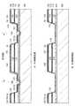
次に、図3の断面図を参照してアレイ装置を構成する個々のVCSELを説明する。本実施例のアレイ装置10は、i型の半絶縁性GaAs基板100上に、n型のGaAs層102を形成し、さらにその上に、Al組成の異なるAlGaAs層を交互に重ねたn型の下部分布ブラック型反射鏡(Distributed Bragg Reflector:以下、DBRという)110、下部DBR110上に形成された、上部および下部スペーサ層に挟まれたInGaAs量子井戸層を含む活性領域112、活性領域112上に形成されたAl組成の異なるAlGaAs層を交互に重ねたp型の上部DBR116を含んで構成される。これらの半導体層は、MOCVDにより形成される。 Next, individual VCSELs constituting the array device will be described with reference to the cross-sectional view of FIG. In the
本実施例のアレイ装置10は、裏面出射、すなわち基板100の裏面からレーザ光を出射させるため、上部DBR116の反射率が下部DBR110の反射率よりも大きくなるように、上部DBR116の低屈折率層と高屈折率層のペアの周期が下部DBR110よりも大きくなるように調整される。n型のGaAs層102は、低抵抗の領域を提供するため下部DBR110よりも高い不純物濃度を有する。また、GaAs層102は、光吸収が大きくならない程度の膜厚に調整される。活性領域112は、980nm帯の波長の光を発生させるが、n型のGaAs層102およびGaAs基板100は、980nm帯の波長を透過する。基板100は、半絶縁性であるため、基板における不純物による光の吸収は抑制される。 Since the
通常のフォトリソ工程を用いて、上部DBR116から下部DBR110に至るまで半導体層をエッチングすることにより、基板100上に円筒状のポスト(柱状構造)Pが形成される。ポストPの形成後の酸化工程において、上部DBR116内の電流狭窄層114は、ポストPの側面から選択的に酸化される。酸化領域により囲まれた酸化アパーチャの径を調整することで、横モード発振が制御される。比較的高出力が要求される場合には、マルチモード発振となる酸化アパーチャ径が選択される。 A cylindrical post (columnar structure) P is formed on the
また、基板上に島領域Sを形成するため、n型のGaAs層102には分離溝104が形成される。分離溝104は、基板100に到達する深さを有することで、島領域は互いに電気的に分離される。 Further, in order to form the island region S on the substrate, a
ポストPおよび分離溝104を含む基板全面に層間絶縁膜118が形成され、層間絶縁膜118の必要な個所にはコンタクトホールCp、Cnが形成される。層間絶縁膜118は、例えば、SiN、SiON等などから構成される。ポストPの頂部には、p型の上部DBR116を露出させるような円形状のコンタクトホールCpが形成される。好ましくは、上部DBR116の最上層には、不純物濃度が高いGaAsコンタクト層が形成され、GaAsコンタクト層は、p側金属120とオーミック接続される。他方、ポストPの間には、ほぼ矩形状のコンタクトホールCnが形成され、コンタクトホールCn内に形成されたn側金属122は、n型のGaAs層102にオーミック接続される。 An interlayer insulating
コンタクトホールCp内のp側金属120は、例えばAu、またはTi/Auなどの積層金属から構成される。コンタクトホールCn内のn側金属122は、n型の半導体層と接続性が良いAu/Geなどから構成される。アノード側の電極パッド130、カソード側の電極パッド140、および中間の金属配線150は、好ましくは同一の金属材料(例えば、p側金属120と同一の材料)から構成され、同時にパターンニングされる。アノード側の電極パッド130のフィンガ部134、および中間の金属配線150のフィンガ部154は、それぞれVCSEL素子のp側金属120に接続され、カソード側の電極パッド140の櫛形部144、および中間の金属配線の櫛形部154は、それぞれポストPの側部のn側金属122に接続される。レーザ光は、基板裏面側から出射されるため、フィンガ部134、154は、ポストPの頂部の全面を覆い、フィンガ部134、154には出射窓または開口は形成されない。 The p-
本実施例のアレイ装置は、1つのチップ上に複数の島領域を形成し、1つの島領域内に複数のVCSEL素子を形成し、複数の島領域間の複数のVCSEL素子をそれぞれ直並列接続する。このように直並列接続されたアレイ装置では、各VCSEL素子を定電流駆動することができ、ムラの少ない均一な面光源を提供することができる。仮に、一部の配線やコンタクトにオープン等の不良が発生しても、アレイ装置の発光を継続させることができる。また、半絶縁性の基板により不純物による光吸収が生じないため、従来のように基板を薄型化する研磨が不要となり、製造工程の容易化を図ることができる。さらに本実施例のアレイ装置では、チップの両端にアノードおよびカソードの電極パッド130、140を配置させ、アレイ状に配列されたVCSEL素子間に中間の金属配線150を配置させることで、基板表面の領域を効果的に利用して金属配線の総面積を大きくすることができ、これにより、金属配線の負荷抵抗を小さくすることでアレイ装置を駆動する電流を低減させ、かつ放熱特性を改善することができる。 In the array apparatus of this embodiment, a plurality of island regions are formed on one chip, a plurality of VCSEL elements are formed in one island region, and a plurality of VCSEL elements between the plurality of island regions are connected in series and parallel. To do. In the array device connected in series and parallel as described above, each VCSEL element can be driven with a constant current, and a uniform surface light source with less unevenness can be provided. Even if a defect such as an open occurs in some wirings or contacts, the array device can continue to emit light. Further, light absorption due to impurities does not occur due to the semi-insulating substrate, so that polishing for thinning the substrate as in the conventional case is unnecessary, and the manufacturing process can be facilitated. Further, in the array apparatus of this embodiment, anode and
次に、本実施例の面発光型半導体レーザアレイ装置の他の構成例について説明する。図6は、他の構成例に係るアレイ装置10Aの概略平面図、図7は、図6のA−A線断面図およびB−B線断面図である。 Next, another configuration example of the surface-emitting type semiconductor laser array device of this embodiment will be described. FIG. 6 is a schematic plan view of an
本構成のアレイ装置10Aは、図6に示すように、コンタクトホールCnの構成を異にし、それに伴い、中間の金属配線150およびカソード側の電極パッド140の一部を変形したものである。コンタクトホールCnは、1つの島領域Sの縁部に沿って列方向に、ポストPと分離溝104との間に複数形成される。ここでは、1つの島領域に4つのポストPが配列されているため、それに応じて4つの矩形状のコンタクトホールCnが形成されている。一方、中間の金属配線150Aは、列方向に延在する部分151と、当該延在する部分151から行方向に延在する複数のフィンガ部154を有しているが、図4の金属配線150のように櫛形部152を備えていない。その代わり、列方向に延在する部分151は、コンタクトホールCn上を延在し、コンタクトホールCnを介してn側金属122に電気的に接続される。カソード側の電極パッド140も同様に、櫛形部を備えておらず、列方向に延在する部分141がコンタクトホールCn上を延在し、n側金属122に電気的に接続される。 As shown in FIG. 6, the
このような構成では、中間の金属配線150Aおよびカソード側の電極パッド140がポストPの間に入り込むような櫛形部を備えていないので、ポストPの列方向のピッチをより狭くすることができ、チップ上に形成されるVCSEL素子の高密度化を図ることができる。 In such a configuration, the
図8は、本実施例のアレイ装置のさらなる他の構成例を示す平面図、図8Aは、図8の表面の金属配線150および電極パッド130、140を取り除いた状態の平面図、図9は、そのA−A線、B−B線断面図である。本構成例のアレイ装置10Bは、n型のGaAs層102への電気的接続を行うためのコンタクトホールCnの構成を異にしている。図8Aに示すように、1つの島領域内に形成されるコンタクトホールCnは、それぞれ分離されるのではなく、1つの連続的な形状を有する。あたかも、図2に示す複数のコンタクトホールCnを、図6に示すコンタクトホールCnにより連結したような形状である。このため、中間の配線金属150の櫛形部152およびカソード側の電極パッド140の櫛形部144の形状に倣うようなコンタクトホールCnが形成され、櫛形部152、144の真下には、比較的大きな面積のn側金属122が形成される。このような構成では、図1の構成と比較して、櫛形部152、144とn型のGaAs層102との間の接触面積を大きくすることができるため、櫛形部152、144での接触抵抗を減らすことができ、同時に、発熱をより効果的に抑制することができる。 FIG. 8 is a plan view showing still another configuration example of the array device of the present embodiment, FIG. 8A is a plan view in a state where the
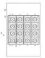
図10は、本実施例のアレイ装置のさらなる他の構成を示す平面図、図10Aは、図10の中間の金属配線および電極パッド130、140を取り除いた状態の平面図、図11は、図10のA−A線断面図、およびB−B線断面図である。本構成例のアレイ装置10Cは、1つ1つのVCSEL素子が完全に分離して形成されるものである。図10Aに示すように、島領域を規定するための分離溝104が格子状に形成され、これにより、行列方向に複数の島領域Sが形成される。図の例では、4行×4列の島領域Sが示されている。そして、1つの島領域Sには、1つのVCSEL素子(またはポストP)が形成され、ポストPの両側に一対のコンタクトホールCnが形成される。アノード側の電極パッド130、カソード側の電極パッド140、および中間の金属配線150の形状は、図1のときと同じである。 10 is a plan view showing still another configuration of the array device of the present embodiment, FIG. 10A is a plan view in a state in which the intermediate metal wiring and
上記実施例では、基板裏面からレーザ光を出射させる例を示したが、これに限らず、基板表面側からレーザ光を出射させるようにしてもよい。この場合には、ポストPの頂部を覆うp側金属120およびフィンガ部134、154に光出射用の開口を形成し、かつ上部DBRよりも下部DBRの反射率が高くなるようにする。 In the above-described embodiment, an example in which laser light is emitted from the back surface of the substrate has been described. In this case, an opening for light emission is formed in the p-
上記実施例では、ポストPを円筒状または円錐状に形成したが、ポストPの形状はどのようなものであってもよい。例えば、ポストPは、1回のエッチングにより連続的に形成してもよいし、複数回のエッチングに分けて形成してもおい。例えば、ポストPを2段階のエッチングにより形成する場合には、最初のエッチングで形成されたポストと次のエッチングで形成されたポストとの境界において不連続な径が生じてもよい。 In the above embodiment, the post P is formed in a cylindrical shape or a conical shape, but the post P may have any shape. For example, the post P may be formed continuously by one etching, or may be divided into a plurality of etchings. For example, when the post P is formed by two-stage etching, a discontinuous diameter may occur at the boundary between the post formed by the first etching and the post formed by the next etching.
さらに上記実施例では、半絶縁性の半導体基板を用いエピタキシャル成長により半導体層を積層する構成を示したが、これに限らず、発振波長を透過できるものであれば、他の絶縁性の基板を用いることも可能である。さらに上記実施例では、基板上にn型のGaAs層を用いたが、共通の導電層は、GaAs以外の半導体材料からなる層であってもよい。さらに上記実施例では、GaAs、AlAs、AlGaAsの半導体材料を用いたGaAs系のVCSELを例示したが、本発明は、他のIII−V族の化合物半導体を用いたVCSELにも適用することができる。 Further, in the above-described embodiment, a configuration in which a semiconductor layer is stacked by epitaxial growth using a semi-insulating semiconductor substrate is shown. However, the present invention is not limited to this, and other insulating substrates can be used as long as they can transmit an oscillation wavelength. It is also possible. Further, in the above embodiment, the n-type GaAs layer is used on the substrate, but the common conductive layer may be a layer made of a semiconductor material other than GaAs. Furthermore, in the above-described embodiment, a GaAs-based VCSEL using a semiconductor material of GaAs, AlAs, or AlGaAs has been exemplified. However, the present invention can also be applied to a VCSEL using another III-V group compound semiconductor. .
次に、本実施例の面発光型半導体レーザアレイ装置を用いた光源の概略断面図を図12に示す。本実施例の光源200は、上記した面発光型半導体レーザアレイ装置10と、アレイ装置10の基板100の裏面上に形成された反射防止膜210と、アレイ装置10の基板の表面側に形成された再配線金属パターン220、再配線金属パターン220上に形成された半田層230、半田層230上に形成されたヒートシンク240、ヒートシンク240上に形成された冷却機器250を含んで構成される。 Next, FIG. 12 shows a schematic sectional view of a light source using the surface-emitting type semiconductor laser array device of this example. The
アレイ装置10は、図1ないし図11に示すような構成を有しており、このアレイ装置10を180度反転した状態が図12に示されている。反射防止膜210は、基板100の裏面に、例えば発振波長のλ/4の膜厚で形成され、アレイ装置10で発光されたレーザ光Lが基板界面で内部に反射されるのを抑制する。 The
アレイ装置10の表面側には、後述するように再配線された金属パターン220が形成される。金属パターン220は、アノード側の電極パッド130とカソード側の電極パッド140に電気的に接続され、それ以外のポストPが形成された発光部領域とは絶縁膜260によって電気的に隔離されている。アノード側の電極パッド130およびカソード側の電極パッド140は、再配線された金属パターン220および半田層230を介してヒートシンク240に接続される。半田層230は、例えばIn半田、Au/Su半田などが用いられる。ヒートシンク240は、例えば熱伝導性が良い銅(Cu)が積層される。冷却機器250は、放熱フィンなどによる空冷装置、冷媒を用いた水冷装置、あるいはペルチエ素子を用いた冷却装置などが用いられる。 On the front surface side of the
図示しない駆動装置から、アノード側の電極パッド130およびカソード側の電極パッド140に順方向駆動電力が供給されると、アレイ装置10の各VCSEL素子が発光し、レーザ光Lが基板裏面から出射される。各VCSEL素子は、定電流駆動されることで、ムラの少ない均一は光を出射する。また、アレイ装置の表面には、再配線された金属パターン220が形成されているため、アレイ装置で発生した熱は、金属パターン220を介して効果的に外部へ放散される。さらに、ヒートシンク240および冷却機器250を設けることで、アレイ装置で発生した熱を強制的に外部へ放散させることで、冷却効率を改善することができる。 When forward drive power is supplied from a driving device (not shown) to the anode-
図13は、図12に示す光源の製造方法を説明する図である。先ず、図13(A)に示すような本実施例のアレイ装置10が作成される。例えば、1mm×1mmのエリア内に、16×16のVCSEL素子が形成される。VCSEL素子のポスト径は約35μm、ビット間隔は65μm、酸化アパーチャ径は25μmである。 FIG. 13 is a diagram for explaining a method of manufacturing the light source shown in FIG. First, the
次に、アレイ装置10の全面を覆うように絶縁膜が塗布され、次いで、図13(B)に示すように、発光領域を覆うように絶縁膜260がパターンニングされる。すなわち、絶縁膜260は、アノード側の電極パッド130の外部接続される領域と、カソード側の電極パッド140の外部接続される領域を露出し、それ以外の発光部領域を被覆するようにパターンニングされる。絶縁膜260は、熱伝導性の高い材料であることが望ましく、例えばポリイミド樹脂が用いられる。このとき、絶縁膜260の表面は平坦化されるようにしてもよい。 Next, an insulating film is applied so as to cover the entire surface of the
次に、アレイ装置10の全面を覆うように金属膜が形成され、次いで、図13(C)に示すように、絶縁膜260上に再配線された金属パターン220が形成される。金属パターン220Aは、アノード側の電極パッド130上に形成され、金属パターン220Bは、カソード側の電極パッド140上に形成される。金属パターン220Cは、金属パターン220A、220Bと分離され、アレイ装置の発光領域を覆う絶縁膜260上に形成される。次に、図13(C)のアレイ装置を反転させ、金属パターン220A、220Bを、半田層230を介してヒートシンク240に接続する。 Next, a metal film is formed so as to cover the entire surface of the
図14は、本実施例の面発光型半導体レーザアレイ装置を用いた光源モジュールの一例を示す平面図である。図14(A)に示すように、本実施例の光源モジュール(レーザバー)300は、線形に配列された複数のアレイ装置10と、アレイ装置10の配列方向に延在するアノード側の金属配線310と、金属配線310と並行に延びるカソード側の金属配線320と、金属配線310と金属配線320間に並行に延びる放熱用の金属配線330とを有する。これらの金属配線は、見易くするためハッチングで表している。アノード側の金属配線310は、各アレイ装置10のアノード側の電極パッド130に共通に電気的に接続され、カソード側の金属配線320は、各アレイ装置10のカソード側の電極パッド140に共通に電気的に接続される。放熱用の金属配線330は、金属配線310、320とは電気的に分離され、絶縁物質を介して各発光装置10の発光部領域を延在し、各アレイ装置で発生した熱を放散させる。 FIG. 14 is a plan view showing an example of a light source module using the surface-emitting type semiconductor laser array device of the present embodiment. As shown in FIG. 14A, the light source module (laser bar) 300 of the present embodiment includes a plurality of
アノード側の電極パッド130およびカソード側の電極パッド140は、半田等を介して金属配線310、320に表面実装することが可能になる。このため、ワイヤボンディング接続をするような光源モジュールと比較して、実装するアレイ装置(チップ)の高密度化が可能になり、製造工程が簡略化され、小型化、薄型化を図ることが可能になる。また、図14(A)の光源モジュール300を、図14(B)に示すように2次元的に配置させることも可能である。このような光源モジュール300を同時に一斉点灯させることで、均一でムラの少ない高光出力の面光源を得ることができる。 The
以上、本発明の好ましい実施の形態について詳述したが、本発明は、特定の実施形態に限定されるものではなく、特許請求の範囲に記載された本発明の要旨の範囲内において、種々の変形・変更が可能である。 The preferred embodiment of the present invention has been described in detail above, but the present invention is not limited to the specific embodiment, and various modifications can be made within the scope of the present invention described in the claims. Deformation / change is possible.
10、10A、10B、10C:面発光型半導体レーザアレイ装置
100:基板
102:n型のGaAs層
104:分離溝
110:下部DBR
112:活性領域
114:電流狭窄層
116:上部DBR
118:層間絶縁膜
120:p側金属
122:n側金属
130:アノード側の電極パッド
132:外部接続部
134:フィンガ部
140:カソード側の電極パッド
142:外部接続部
144:櫛形部
146:空間
150:中間の金属配線
151:列方向に延在する部分
152:櫛形部
154:フィンガ部
156:空間
Cn、Cp:コンタクトホール
S、SA、SC:島領域
10, 10A, 10B, 10C: surface emitting semiconductor laser array device 100: substrate 102: n-type GaAs layer 104: separation groove 110: lower DBR
112: Active region 114: Current confinement layer 116: Upper DBR
118: Interlayer insulating film 120: p-side metal 122: n-side metal 130: anode-side electrode pad 132: external connection part 134: finger part 140: cathode-side electrode pad 142: external connection part 144: comb-shaped part 146: space 150:
Claims (18)
Translated fromJapanese前記基板の第1の主面上に行列状に配された複数の面発光型半導体レーザ素子と、
前記基板の第1の主面上に形成され、第1の列に配された複数の面発光型半導体レーザ素子の第1の電極に並列に電気的接続された第1の電極領域と、
前記基板の第1の主面上に形成され、第2の列に配された複数の面発光型半導体レーザ素子の第2の電極に並列に電気的接続された第2の電極領域と、
前記第1の電極領域と前記第2の電極領域との間に配された少なくとも1つの金属配線とを有し、
前記金属配線は、一方の列と他方の列の間を列方向に延在する部分を含み、かつ一方の列の複数の面発光型半導体レーザ素子の第1の電極にそれぞれ電気的に接続された第1の接続部と、他方の列の複数の面発光型半導体レーザ素子の第2の電極にそれぞれ電気的に接続された第2の接続部とを有する、面発光型半導体レーザアレイ装置。A substrate having a first main surface, a second main surface opposite to the first main surface;
A plurality of surface-emitting type semiconductor laser elements arranged in a matrix on the first main surface of the substrate;
A first electrode region formed on the first main surface of the substrate and electrically connected in parallel to the first electrodes of the plurality of surface emitting semiconductor laser elements arranged in the first row;
A second electrode region formed on the first main surface of the substrate and electrically connected in parallel to the second electrodes of the plurality of surface-emitting type semiconductor laser elements arranged in the second row;
Having at least one metal wiring disposed between the first electrode region and the second electrode region;
The metal wiring includes a portion extending in the column direction between one column and the other column, and is electrically connected to the first electrodes of the plurality of surface-emitting type semiconductor laser elements in one column, respectively. A surface-emitting type semiconductor laser array device comprising: a first connection portion; and a second connection portion electrically connected to the second electrodes of the plurality of surface-emitting type semiconductor laser elements in the other column.
前記第1の接続部の櫛形部の各々は、一方の列の複数の面発光型半導体レーザ素子の各々の間を延在する、請求項1または2に記載の面発光型半導体レーザアレイ装置。The first connection portion includes a plurality of comb-shaped portions extending in the first row direction, and the second connection portion is different from the comb-shaped portion of the first connection portion in the second position. A plurality of comb-shaped portions extending in the row direction of
3. The surface-emitting type semiconductor laser array device according to claim 1, wherein each of the comb-shaped portions of the first connection portion extends between each of the plurality of surface-emitting type semiconductor laser elements in one row.
前記面発光型半導体レーザアレイ装置を駆動する駆動手段と、
前記面発光型半導体レーザアレイ装置に熱的に結合され、前記面発光型半導体レーザアレイ装置で発生された熱を放熱させる放熱手段と、
を有する光源。A surface-emitting type semiconductor laser array device according to any one of claims 1 to 15,
Driving means for driving the surface-emitting type semiconductor laser array device;
A heat radiating means thermally coupled to the surface emitting semiconductor laser array device and radiating heat generated by the surface emitting semiconductor laser array device;
Having a light source.
複数の面発光型半導体レーザアレイ装置の配列方向と並行に延在するアノード側の金属配線、カソード側の金属配線、および放熱用の金属配線とを含み、
前記アノード側の金属配線は、複数の面発光型半導体レーザアレイ装置のアノード側電極パッドに共通に電気的に接続され、前記カソード側の金属配線は、複数の面発光型半導体レーザアレイ装置のカソード側電極パッドに共通に電気的に接続され、前記放熱用の金属配線は、前記アノード側の金属配線と前記カソード側の金属配線の間に配列される、光源モジュール。A plurality of surface-emitting type semiconductor laser array devices according to any one of claims 1 to 15,
Including metal wiring on the anode side, metal wiring on the cathode side, and metal wiring for heat dissipation extending in parallel with the arrangement direction of the plurality of surface emitting semiconductor laser array devices,
The anode-side metal wiring is electrically connected in common to anode-side electrode pads of a plurality of surface-emitting type semiconductor laser array devices, and the cathode-side metal wiring is a cathode of a plurality of surface-emitting type semiconductor laser array devices. The light source module is electrically connected in common to a side electrode pad, and the metal wiring for heat dissipation is arranged between the metal wiring on the anode side and the metal wiring on the cathode side.
18. The light source module according to claim 17, wherein anode-side electrode pads and cathode-side electrode pads of the plurality of surface-emitting type semiconductor laser array devices are surface-mounted on the anode-side metal wiring and the cathode-side metal wiring.
Priority Applications (1)
| Application Number | Priority Date | Filing Date | Title |
|---|---|---|---|
| JP2012244089AJP6083194B2 (en) | 2012-11-06 | 2012-11-06 | Surface emitting semiconductor laser array device, light source and light source module |
Applications Claiming Priority (1)
| Application Number | Priority Date | Filing Date | Title |
|---|---|---|---|
| JP2012244089AJP6083194B2 (en) | 2012-11-06 | 2012-11-06 | Surface emitting semiconductor laser array device, light source and light source module |
Publications (2)
| Publication Number | Publication Date |
|---|---|
| JP2014093463Atrue JP2014093463A (en) | 2014-05-19 |
| JP6083194B2 JP6083194B2 (en) | 2017-02-22 |
Family
ID=50937326
Family Applications (1)
| Application Number | Title | Priority Date | Filing Date |
|---|---|---|---|
| JP2012244089AExpired - Fee RelatedJP6083194B2 (en) | 2012-11-06 | 2012-11-06 | Surface emitting semiconductor laser array device, light source and light source module |
Country Status (1)
| Country | Link |
|---|---|
| JP (1) | JP6083194B2 (en) |
Cited By (15)
| Publication number | Priority date | Publication date | Assignee | Title |
|---|---|---|---|---|
| KR20170022754A (en)* | 2015-08-21 | 2017-03-02 | 엘지전자 주식회사 | Lighting source module package |
| CN110137803A (en)* | 2019-05-26 | 2019-08-16 | 杭州晟创激光科技有限公司 | A kind of laser (VCSEL) encapsulating structure |
| CN111149226A (en)* | 2017-07-25 | 2020-05-12 | 三流明公司 | Single chip series connection VCSEL array |
| WO2021033439A1 (en)* | 2019-08-20 | 2021-02-25 | ソニーセミコンダクタソリューションズ株式会社 | Semiconductor laser drive device, electronic apparatus, and method for manufacturing semiconductor laser drive device |
| JP2021068920A (en)* | 2021-02-02 | 2021-04-30 | 富士ゼロックス株式会社 | Light-emitting element array |
| CN113258449A (en)* | 2021-04-27 | 2021-08-13 | 深圳市安思疆科技有限公司 | Laser light source partition packaging structure for dTOF ranging system |
| CN113396477A (en)* | 2019-02-04 | 2021-09-14 | 索尼半导体解决方案公司 | Electronic device |
| JP2022506089A (en)* | 2018-11-08 | 2022-01-17 | オスラム オプト セミコンダクターズ ゲゼルシャフト ミット ベシュレンクテル ハフツング | How to operate diode laser and diode laser |
| CN114142346A (en)* | 2020-09-04 | 2022-03-04 | 浙江睿熙科技有限公司 | Monolithic integrated VCSEL chip |
| JP2022139943A (en)* | 2021-03-12 | 2022-09-26 | 株式会社リコー | Surface emitting laser array, light source module and rangefinder |
| CN115117735A (en)* | 2021-03-17 | 2022-09-27 | 上海禾赛科技有限公司 | Laser, light source module and laser radar |
| US11482835B2 (en) | 2017-07-25 | 2022-10-25 | Lumentum Operations Llc | VCSEL device with multiple stacked active regions |
| CN115308710A (en)* | 2021-04-20 | 2022-11-08 | 锐驰智光(北京)科技有限公司 | Array type laser emission module and laser radar with same |
| CN115407314A (en)* | 2021-05-26 | 2022-11-29 | 锐驰智光(北京)科技有限公司 | Laser emission module and laser radar with same |
| CN115668667A (en)* | 2020-05-21 | 2023-01-31 | 索尼半导体解决方案公司 | Light emitting element array |
Citations (10)
| Publication number | Priority date | Publication date | Assignee | Title |
|---|---|---|---|---|
| JPS5136085A (en)* | 1974-09-24 | 1976-03-26 | Mitsubishi Electric Corp | |
| JPS6072281A (en)* | 1983-09-28 | 1985-04-24 | Sanyo Electric Co Ltd | Led substrate |
| JPS63306687A (en)* | 1987-06-08 | 1988-12-14 | Fujitsu Ltd | Manufacture of semiconductor light-emitting device |
| US20050225973A1 (en)* | 2004-04-02 | 2005-10-13 | Gelcore, Llc | LED with series-connected monolithically integrated mesas |
| JP2009094308A (en)* | 2007-10-10 | 2009-04-30 | Fuji Xerox Co Ltd | Semiconductor light emitting module |
| WO2010035788A1 (en)* | 2008-09-25 | 2010-04-01 | デンカAgsp株式会社 | Substrate for mounting light-emitting element and method for producing same |
| JP2010517273A (en)* | 2007-01-22 | 2010-05-20 | クリー レッド ライティング ソリューションズ、インコーポレイテッド | Fault tolerant illuminant, system including fault tolerant illuminant and method for making fault tolerant illuminant |
| WO2010084890A1 (en)* | 2009-01-20 | 2010-07-29 | 古河電気工業株式会社 | Two-dimensional surface-light-emitting laser array element, surface-light-emitting laser device, and light source |
| JP2011181925A (en)* | 2010-02-27 | 2011-09-15 | Samsung Led Co Ltd | Semiconductor light emitting device including multi-cell array, light emitting module, and lighting system |
| JP2012028412A (en)* | 2010-07-20 | 2012-02-09 | Furukawa Electric Co Ltd:The | Two-dimensional surface emitting laser array element, surface emitting laser device, and light source |
- 2012
- 2012-11-06JPJP2012244089Apatent/JP6083194B2/ennot_activeExpired - Fee Related
Patent Citations (10)
| Publication number | Priority date | Publication date | Assignee | Title |
|---|---|---|---|---|
| JPS5136085A (en)* | 1974-09-24 | 1976-03-26 | Mitsubishi Electric Corp | |
| JPS6072281A (en)* | 1983-09-28 | 1985-04-24 | Sanyo Electric Co Ltd | Led substrate |
| JPS63306687A (en)* | 1987-06-08 | 1988-12-14 | Fujitsu Ltd | Manufacture of semiconductor light-emitting device |
| US20050225973A1 (en)* | 2004-04-02 | 2005-10-13 | Gelcore, Llc | LED with series-connected monolithically integrated mesas |
| JP2010517273A (en)* | 2007-01-22 | 2010-05-20 | クリー レッド ライティング ソリューションズ、インコーポレイテッド | Fault tolerant illuminant, system including fault tolerant illuminant and method for making fault tolerant illuminant |
| JP2009094308A (en)* | 2007-10-10 | 2009-04-30 | Fuji Xerox Co Ltd | Semiconductor light emitting module |
| WO2010035788A1 (en)* | 2008-09-25 | 2010-04-01 | デンカAgsp株式会社 | Substrate for mounting light-emitting element and method for producing same |
| WO2010084890A1 (en)* | 2009-01-20 | 2010-07-29 | 古河電気工業株式会社 | Two-dimensional surface-light-emitting laser array element, surface-light-emitting laser device, and light source |
| JP2011181925A (en)* | 2010-02-27 | 2011-09-15 | Samsung Led Co Ltd | Semiconductor light emitting device including multi-cell array, light emitting module, and lighting system |
| JP2012028412A (en)* | 2010-07-20 | 2012-02-09 | Furukawa Electric Co Ltd:The | Two-dimensional surface emitting laser array element, surface emitting laser device, and light source |
Cited By (26)
| Publication number | Priority date | Publication date | Assignee | Title |
|---|---|---|---|---|
| KR102429095B1 (en) | 2015-08-21 | 2022-08-04 | 엘지전자 주식회사 | Lighting source module package |
| KR20170022754A (en)* | 2015-08-21 | 2017-03-02 | 엘지전자 주식회사 | Lighting source module package |
| US11482835B2 (en) | 2017-07-25 | 2022-10-25 | Lumentum Operations Llc | VCSEL device with multiple stacked active regions |
| CN111149226B (en)* | 2017-07-25 | 2023-04-18 | 朗美通经营有限责任公司 | Single chip series connection VCSEL array |
| JP2020529128A (en)* | 2017-07-25 | 2020-10-01 | トリルミナ コーポレーション | Single chip series connection VCSEL array |
| JP7128259B2 (en) | 2017-07-25 | 2022-08-30 | ルメンタム・オペレーションズ・リミテッド・ライアビリティ・カンパニー | Single-chip series-connected VCSEL array |
| CN111149226A (en)* | 2017-07-25 | 2020-05-12 | 三流明公司 | Single chip series connection VCSEL array |
| JP2022506089A (en)* | 2018-11-08 | 2022-01-17 | オスラム オプト セミコンダクターズ ゲゼルシャフト ミット ベシュレンクテル ハフツング | How to operate diode laser and diode laser |
| JP7258134B2 (en) | 2018-11-08 | 2023-04-14 | エイエムエス-オスラム インターナショナル ゲーエムベーハー | Diode laser and method of operation of diode laser |
| US12021351B2 (en) | 2018-11-08 | 2024-06-25 | Osram Opto Semiconductors Gmbh | Diode laser and method for operating a diode laser |
| CN113396477A (en)* | 2019-02-04 | 2021-09-14 | 索尼半导体解决方案公司 | Electronic device |
| TWI877132B (en)* | 2019-02-04 | 2025-03-21 | 日商索尼半導體解決方案公司 | Electronic device |
| CN110137803A (en)* | 2019-05-26 | 2019-08-16 | 杭州晟创激光科技有限公司 | A kind of laser (VCSEL) encapsulating structure |
| US12327980B2 (en) | 2019-08-20 | 2025-06-10 | Sony Semiconductor Solutions Corporation | Semiconductor laser driving apparatus, electronic equipment, and manufacturing method of semiconductor laser driving apparatus |
| WO2021033439A1 (en)* | 2019-08-20 | 2021-02-25 | ソニーセミコンダクタソリューションズ株式会社 | Semiconductor laser drive device, electronic apparatus, and method for manufacturing semiconductor laser drive device |
| CN115668667B (en)* | 2020-05-21 | 2025-09-26 | 索尼半导体解决方案公司 | Light-emitting element array |
| CN115668667A (en)* | 2020-05-21 | 2023-01-31 | 索尼半导体解决方案公司 | Light emitting element array |
| CN114142346A (en)* | 2020-09-04 | 2022-03-04 | 浙江睿熙科技有限公司 | Monolithic integrated VCSEL chip |
| JP7151803B2 (en) | 2021-02-02 | 2022-10-12 | 富士フイルムビジネスイノベーション株式会社 | light emitting element array |
| JP2021068920A (en)* | 2021-02-02 | 2021-04-30 | 富士ゼロックス株式会社 | Light-emitting element array |
| JP2022139943A (en)* | 2021-03-12 | 2022-09-26 | 株式会社リコー | Surface emitting laser array, light source module and rangefinder |
| JP7683252B2 (en) | 2021-03-12 | 2025-05-27 | 株式会社リコー | Surface emitting laser array, light source module and distance measuring device |
| CN115117735A (en)* | 2021-03-17 | 2022-09-27 | 上海禾赛科技有限公司 | Laser, light source module and laser radar |
| CN115308710A (en)* | 2021-04-20 | 2022-11-08 | 锐驰智光(北京)科技有限公司 | Array type laser emission module and laser radar with same |
| CN113258449A (en)* | 2021-04-27 | 2021-08-13 | 深圳市安思疆科技有限公司 | Laser light source partition packaging structure for dTOF ranging system |
| CN115407314A (en)* | 2021-05-26 | 2022-11-29 | 锐驰智光(北京)科技有限公司 | Laser emission module and laser radar with same |
Also Published As
| Publication number | Publication date |
|---|---|
| JP6083194B2 (en) | 2017-02-22 |
Similar Documents
| Publication | Publication Date | Title |
|---|---|---|
| JP6083194B2 (en) | Surface emitting semiconductor laser array device, light source and light source module | |
| JP6176298B2 (en) | Surface emitting semiconductor laser array and method for manufacturing surface emitting semiconductor laser array | |
| JP2023522559A (en) | 3D and LiDAR sensing module | |
| JP4160597B2 (en) | Semiconductor light emitting device and manufacturing method thereof | |
| JPH11168262A (en) | Surface type optical device, manufacturing method thereof, and display device | |
| US7813402B2 (en) | Surface emitting laser and method of manufacturing the same | |
| JP2013065692A (en) | Surface emitting semiconductor laser, surface emitting semiconductor laser device, optical transmission device and information processing unit | |
| JP6216785B2 (en) | VCSEL with contact in cavity | |
| JP6252222B2 (en) | Surface emitting laser array and laser apparatus | |
| JP6308319B2 (en) | Surface emitting semiconductor laser array | |
| JP2000049414A (en) | Optical function element device, optical transmitting / receiving device using the same, optical interconnection device, and optical recording device | |
| KR101248553B1 (en) | Light emitting device | |
| US20200350742A1 (en) | Laser device | |
| JP3797748B2 (en) | Light emitting diode array | |
| JP2005079580A (en) | Laser apparatus having multiple light emitting regions | |
| US20220158413A1 (en) | Semiconductor laser | |
| WO2019107273A1 (en) | Surface emission semiconductor laser | |
| JP2009158709A (en) | Surface emitting semiconductor laser array and surface emitting semiconductor laser | |
| WO2021230004A1 (en) | Light-emitting device | |
| JP2013179210A (en) | Array type semiconductor laser device and manufacturing method thereof | |
| US20250056930A1 (en) | Semiconductor device | |
| US20250149852A1 (en) | Package assembly for vertical cavity surface emitting laser device on a driver ic | |
| US20230101361A1 (en) | Method for manufacturing diffusion cover, diffusion cover, and semiconductor light-emitting device comprising same | |
| US7643531B2 (en) | Optical semiconductor element including photodetecting element with comb-tooth structure | |
| JP2023060843A (en) | Optical semiconductor element |
Legal Events
| Date | Code | Title | Description |
|---|---|---|---|
| A621 | Written request for application examination | Free format text:JAPANESE INTERMEDIATE CODE: A621 Effective date:20150819 | |
| A977 | Report on retrieval | Free format text:JAPANESE INTERMEDIATE CODE: A971007 Effective date:20160523 | |
| A131 | Notification of reasons for refusal | Free format text:JAPANESE INTERMEDIATE CODE: A131 Effective date:20160621 | |
| A521 | Request for written amendment filed | Free format text:JAPANESE INTERMEDIATE CODE: A523 Effective date:20160808 Free format text:JAPANESE INTERMEDIATE CODE: A821 Effective date:20160808 | |
| TRDD | Decision of grant or rejection written | ||
| A01 | Written decision to grant a patent or to grant a registration (utility model) | Free format text:JAPANESE INTERMEDIATE CODE: A01 Effective date:20161227 | |
| A61 | First payment of annual fees (during grant procedure) | Free format text:JAPANESE INTERMEDIATE CODE: A61 Effective date:20170109 | |
| R150 | Certificate of patent or registration of utility model | Ref document number:6083194 Country of ref document:JP Free format text:JAPANESE INTERMEDIATE CODE: R150 | |
| S533 | Written request for registration of change of name | Free format text:JAPANESE INTERMEDIATE CODE: R313533 | |
| R350 | Written notification of registration of transfer | Free format text:JAPANESE INTERMEDIATE CODE: R350 | |
| LAPS | Cancellation because of no payment of annual fees |