JP2014082736A - Array antenna device - Google Patents
Array antenna deviceDownload PDFInfo
- Publication number
- JP2014082736A JP2014082736AJP2013045599AJP2013045599AJP2014082736AJP 2014082736 AJP2014082736 AJP 2014082736AJP 2013045599 AJP2013045599 AJP 2013045599AJP 2013045599 AJP2013045599 AJP 2013045599AJP 2014082736 AJP2014082736 AJP 2014082736A
- Authority
- JP
- Japan
- Prior art keywords
- ground conductor
- array antenna
- conductor
- excitation
- axial ratio
- Prior art date
- Legal status (The legal status is an assumption and is not a legal conclusion. Google has not performed a legal analysis and makes no representation as to the accuracy of the status listed.)
- Pending
Links
- 239000004020conductorSubstances0.000claimsabstractdescription175
- 230000003071parasitic effectEffects0.000claimsabstractdescription10
- 230000005284excitationEffects0.000claimsdescription100
- 238000010586diagramMethods0.000description34
- 238000004088simulationMethods0.000description30
- 230000010287polarizationEffects0.000description28
- 238000001514detection methodMethods0.000description22
- 230000005855radiationEffects0.000description14
- 230000006870functionEffects0.000description9
- 230000000694effectsEffects0.000description4
- 230000007423decreaseEffects0.000description2
- 238000004364calculation methodMethods0.000description1
- 239000003990capacitorSubstances0.000description1
- 238000006243chemical reactionMethods0.000description1
- 230000002500effect on skinEffects0.000description1
- 238000002474experimental methodMethods0.000description1
- 230000003993interactionEffects0.000description1
- 239000000463materialSubstances0.000description1
- 238000000034methodMethods0.000description1
Images


Landscapes
- Aerials With Secondary Devices (AREA)
- Variable-Direction Aerials And Aerial Arrays (AREA)
- Radar Systems Or Details Thereof (AREA)
Abstract
Description
Translated fromJapanese本発明は、アレーアンテナ装置に関し、特に、アレーアンテナ装置の軸比を改善する技術に関する。 The present invention relates to an array antenna device, and more particularly to a technique for improving the axial ratio of an array antenna device.
アレーアンテナ装置として、無線信号を受信するための励振素子と、その励振素子から所定の間隔だけ離れて設けられた複数の非励振素子とを備え、各非励振素子にそれぞれ接続された複数の可変リアクタンス素子のリアクタンス値が変化することにより、指向性が変化するアレーアンテナ装置が知られている(たとえば、特許文献1)。なお、この形式のアレーアンテナ装置は、電子走査導波器アレーアンテナ装置と呼ばれることも多いが、以下では、単にアレーアンテナ装置という。 The array antenna apparatus includes an excitation element for receiving a radio signal, and a plurality of non-excitation elements provided at a predetermined distance from the excitation element, and a plurality of variable elements connected to the respective non-excitation elements. An array antenna apparatus is known in which directivity changes as a reactance value of a reactance element changes (for example, Patent Document 1). An array antenna apparatus of this type is often called an electronic scanning waveguide array antenna apparatus, but is simply referred to as an array antenna apparatus below.
アレーアンテナ装置では、励振素子および非励振素子は、円形の接地導体上に、その接地導体から絶縁された状態で設けられる。また、一般的に、接地導体は、半径が受信電波の波長λの1/2に設定される。励振素子は、この接地導体の中心に配置され、非励振素子は、接地導体の中心からの距離が波長λの1/4となるように配置され、各非励振素子には可変リアクタンス素子が接続される。上記位置に非励振素子が配置されると、可変リアクタンス素子のリアクタンス値を変化させることで、非励振素子を、導波器や反射器として機能させることができる。よって、指向性が可変となる。 In the array antenna apparatus, the excitation element and the non-excitation element are provided on a circular ground conductor in a state of being insulated from the ground conductor. In general, the radius of the ground conductor is set to ½ of the wavelength λ of the received radio wave. The excitation element is arranged at the center of the ground conductor, the non-excitation element is arranged so that the distance from the center of the ground conductor is 1/4 of the wavelength λ, and a variable reactance element is connected to each non-excitation element. Is done. When the non-exciting element is disposed at the above position, the non-exciting element can function as a director or a reflector by changing the reactance value of the variable reactance element. Therefore, directivity is variable.
このアレーアンテナ装置は、指向性が可変であることを利用して、無線端末(たとえば、無線タグ)の方向探知に用いられることがある。アレーアンテナ装置は、通常、水平面走査となるように設置され、この場合、垂直偏波に対して良好な指向性を有する。したがって、方向探知の対象となる無線タグが垂直偏波を送信すれば、精度のよい方向探知が可能になる。 This array antenna apparatus may be used for direction detection of a wireless terminal (for example, a wireless tag) by utilizing the fact that directivity is variable. The array antenna apparatus is usually installed so as to perform horizontal plane scanning, and in this case, has good directivity with respect to vertical polarization. Therefore, if the wireless tag that is the target of direction detection transmits vertical polarization, direction detection with high accuracy becomes possible.
しかし、無線タグが人に携帯される場合は、無線タグが様々な向きとなる。従って、無線タグが送信する電波は、水平偏波が主放射偏波となることもある。アレーアンテナ装置は水平偏波に対する指向性は必ずしも垂直偏波の指向性と合致しないことから、水平偏波によって無線タグの方向を推定すると、その精度が十分に得られない。そこで、無線タグが送信する電波は水平偏波成分が強く、垂直偏波成分が弱い場合であっても、アレーアンテナ装置は、垂直偏波成分に基づいた方向推定を行なうことが望まれる。そのためには、アレーアンテナ装置は、垂直偏波の利得が水平偏波の利得よりもできるだけ高いことが望まれる。 However, when the wireless tag is carried by a person, the wireless tag is in various directions. Therefore, in the radio wave transmitted by the wireless tag, the horizontal polarization may become the main radiation polarization. Since the directivity with respect to horizontal polarization does not necessarily match the directivity with vertical polarization in the array antenna apparatus, if the direction of the wireless tag is estimated with horizontal polarization, the accuracy cannot be sufficiently obtained. Therefore, even if the radio wave transmitted by the wireless tag has a strong horizontal polarization component and a weak vertical polarization component, it is desired that the array antenna apparatus perform direction estimation based on the vertical polarization component. For this purpose, the array antenna device is desired to have a vertical polarization gain as high as possible as compared to a horizontal polarization gain.
ここで、主放射成分利得と、その主放射成分と直交する偏波の利得との比を軸比という。アレーアンテナ装置では、垂直偏波が受信する主放射成分となることが要求されるから、垂直偏波を主放射成分としてみた場合、主放射成分の軸比が大きいほど、水平偏波の利得と比較して垂直偏波の利得が高いことを意味する。よって、アレーアンテナ装置では、受信時におけるこの垂直偏波を主放射成分としてみた場合の主放射成分の軸比を大きくすることが望まれることになる。特許文献1には、軸比を改善するとの明確な記載はないものの、接地導体(特許文献1では有限反射板1)の半径を大きくすることによって水平面の主放射成分利得を高くし、受信時の軸比を改善できることが推測できる(段落0017など)。 Here, the ratio between the main radiation component gain and the gain of the polarization orthogonal to the main radiation component is referred to as an axial ratio. In an array antenna apparatus, vertical polarization is required to be the main radiation component to be received. Therefore, when viewing vertical polarization as the main radiation component, the larger the axial ratio of the main radiation component, the higher the gain of horizontal polarization. This means that the gain of vertical polarization is high. Therefore, in the array antenna apparatus, it is desired to increase the axial ratio of the main radiation component when the vertically polarized wave at the time of reception is viewed as the main radiation component. Although there is no clear description in
しかしながら、接地導体半径を大きくしてしまうと、アレーアンテナ装置が大型化してしまうので好ましくない。 However, if the radius of the ground conductor is increased, the array antenna device is increased in size, which is not preferable.
本発明は、この事情に基づいて成されたものであり、その目的とするところは、装置の大型化を抑制しつつ、軸比を改善することができるアレーアンテナ装置を提供することにある。 The present invention has been made based on this situation, and an object of the present invention is to provide an array antenna device capable of improving the axial ratio while suppressing an increase in size of the device.
その目的を達成するための請求項1記載の発明は、
円形の接地導体と、
前記接地導体の中心に、その接地導体から絶縁された状態で設けられ、無線信号を受信する励振素子と、
前記接地導体上にその接地導体から絶縁された状態で設けられた複数の非励振素子と、
各非励振素子にそれぞれ接続された複数の可変リアクタンス素子と、を備え、
可変リアクタンス素子のリアクタンス値が変化することにより、前記複数の非励振素子が導波器あるいは反射器として機能するように、それら複数の非励振素子は、前記励振素子から所定の素子間距離だけ離隔して配置されているアレーアンテナ装置であって、
前記接地導体に対して前記励振素子および非励振素子側に導体円環板が配置されており、且つ、その導体円環板は、
前記接地導体と平行であり、
中心軸線が前記接地導体の中心軸線と一致し、
前記接地導体の上面と導体円環板の下面との間の距離d、導体円環板の内半径rin、外半径routが、前記励振素子の長さをL、アレーアンテナ装置が受信する電波の波長をλとしたとき、下記(1)〜(8)のいずれかの条件を満たしていることを特徴とするアレーアンテナ装置。
1.0<d<0.24Lの場合
(1) 素子間距離<rin<0.35λ、 0.40λ≦rout≦0.74λ
(2) 0.35λ≦rin<rout≦0.74λ
2.0.24L≦d<0.35Lの場合
(3) 素子間距離<rin<0.35λ、 0.35λ≦rout≦0.74λ
(4) 0.35λ≦rin<rout≦0.74λ
3.0.35L≦d<0.43Lの場合
(5) 素子間距離<rin<0.30λ、 rin<rout≦0.74λ
(6) 0.30λ≦rin<0.35λ、 0.35λ≦rout≦0.74λ
(7) 0.35λ≦rin<rout≦0.74λ
4.0.43L≦d<1.00Lの場合
(8) 素子間距離<rin<rout≦0.74λIn order to achieve the object, the invention according to
A circular ground conductor;
An excitation element provided at the center of the ground conductor in a state insulated from the ground conductor and receiving a radio signal;
A plurality of parasitic elements provided on the ground conductor in a state of being insulated from the ground conductor;
A plurality of variable reactance elements respectively connected to each non-excitation element,
The plurality of non-excitation elements are separated from the excitation elements by a predetermined inter-element distance so that the reactance values of the variable reactance elements change so that the plurality of non-excitation elements function as a director or a reflector. An array antenna device arranged as
A conductor ring plate is disposed on the excitation element and non-excitation element side with respect to the ground conductor, and the conductor ring plate is
Parallel to the ground conductor;
The central axis coincides with the central axis of the ground conductor;
The distance d between the upper surface of the ground conductor and the lower surface of the conductor ring plate, the inner radius rin and the outer radius rout of the conductor ring plate are L, and the array antenna apparatus receives the length of the excitation element. An array antenna apparatus characterized by satisfying any of the following conditions (1) to (8), where λ is the wavelength of the radio wave.
When 1.0 <d <0.24L (1) Inter-element distance <rin <0.35λ, 0.40λ ≦ rout ≦ 0.74λ
(2) 0.35λ ≦ rin <rout ≦ 0.74λ
2. In the case of 0.24L ≦ d <0.35L (3) Inter-element distance <rin <0.35λ, 0.35λ ≦ rout ≦ 0.74λ
(4) 0.35λ ≦ rin <rout ≦ 0.74λ
3. When 0.35L ≦ d <0.43L (5) Distance between elements <rin <0.30λ, rin <rout ≦ 0.74λ
(6) 0.30λ ≦ rin <0.35λ, 0.35λ ≦ rout ≦ 0.74λ
(7) 0.35λ ≦ rin <rout ≦ 0.74λ
4. In the case of 0.43L ≦ d <1.00L (8) Distance between elements <rin <rout ≦ 0.74λ
上記条件を満たす導体円環板を備えたアレーアンテナ装置は、導体円環板がない以外は同じ構成のアレーアンテナ装置(以下、従来アレーアンテナ装置)に比較して、受信された時の軸比が大きくなることをシミュレーションにより確認できた(なお、シミュレーション結果は後に詳述する)。 The array antenna device having a conductor ring plate that satisfies the above conditions is compared with an array antenna device having the same configuration except that there is no conductor ring plate (hereinafter referred to as a conventional array antenna device). It has been confirmed by simulation that the value becomes large (the simulation result will be described in detail later).
しかも、導体円環板は、励振素子や非励振素子の上端よりも接地導体に近い位置ないしはその上端とほぼ同じ位置に配置されるので、アレーアンテナ装置の高さ方向寸法はほとんど大きくならない。よって、装置の大型化を抑制しつつ、軸比を改善することができる。 In addition, since the conductor annular plate is disposed at a position closer to the ground conductor than the upper ends of the excitation elements and the non-excitation elements, or at substantially the same position as the upper end thereof, the dimension in the height direction of the array antenna device is hardly increased. Therefore, the axial ratio can be improved while suppressing an increase in the size of the apparatus.
また、請求項2記載のように、前記(1)〜(8)のいずれかの条件において、外半径routの上限値を前記接地導体の半径に置き換えた条件を満たしていることが好ましい。According to a second aspect of the present invention, it is preferable that, in any one of the conditions (1) to (8), the condition that the upper limit value of the outer radius rout is replaced with the radius of the ground conductor is satisfied.
このようにすれば、導体円環板を設けても、アレーアンテナ装置は、径方向寸法も大きくならない。 In this way, even if a conductor ring plate is provided, the array antenna device does not have a large radial dimension.
また、前述の目的を達成するための請求項3記載の発明は、
円形の接地導体と、
前記接地導体の中心に、その接地導体から絶縁された状態で設けられ、無線信号を受信する励振素子と、
前記接地導体上にその接地導体から絶縁された状態で設けられた複数の非励振素子と、
各非励振素子にそれぞれ接続された複数の可変リアクタンス素子と、を備え、
可変リアクタンス素子のリアクタンス値が変化することにより、前記複数の非励振素子が導波器あるいは反射器として機能するように、それら複数の非励振素子は、前記励振素子から所定の素子間距離だけ離隔して配置されているアレーアンテナ装置であって、
前記接地導体に対して前記励振素子および非励振素子側に導体円環板が配置されており、且つ、その導体円環板は、
前記接地導体と平行であり、
中心軸線が前記接地導体の中心軸線と一致し、
前記励振素子の上端と前記導体円環板の下面との間の距離D、導体円環板の内半径rin、外半径routが、アレーアンテナ装置が受信する電波の波長をλとしたとき、下記
(1)〜(19)のいずれかの条件を満たしていることを特徴とするアレーアンテナ装置。
1.0≦D<0.03λの場合
(1) 0<rin<0.17λ、 0.34λ≦rout≦0.61λ
(2) 0.17λ≦rin<0.25λ、 0.30λ≦rout≦0.65λ
(3) 0.25λ≦rin<0.33λ、 rin<rout<0.65λ
(4) 0.33λ≦rin<rout≦0.74λ
2.0.03λ≦D<0.05λの場合
(5) 0<rin<0.21λ、 0.34λ≦rout≦0.61λ
(6) 0.21λ≦rin<0.33λ、 0.30λ≦rout≦0.61λ
(7) 0.33λ≦rin<rout≦0.74λ
3.0.05λ≦D<0.07λの場合
(8) 0<rin<0.25λ、 0.38λ≦rout≦0.61λ
(9) 0.25λ≦rin<0.33λ、 0.34λ≦rout≦0.62λ
(10) 0.33λ≦rin<rout≦0.74λ
4.0.07λ≦D<0.14λの場合
(11) 0<rin<0.25λ、 0.34λ≦rout≦0.62λ
(12) 0.25λ≦rin<0.33λ、 0.34λ≦rout≦0.66λ
(13) 0.33λ≦rin<rout≦0.74λ
5.0.14λ≦D<0.23λの場合
(14) 0<rin<0.33λ、 0.34λ≦rout≦0.74λ
(15) 0.33λ≦rin<rout≦0.74λ
6.0.23λ≦D<0.24λの場合
(16) 0<rin<0.37λ、 0.34λ≦rout≦0.74λ
(17) 0.37λ≦rin≦0.49λ、 0.46λ≦rout≦0.74λ
7.0.24λ≦D<0.29λの場合
(18) 0<rin<0.37λ、 0.34λ≦rout≦0.66λ
(19) 0.33λ<rin≦0.49λ、 0.50λ≦rout≦0.66λIn order to achieve the above object, the invention according to
A circular ground conductor;
An excitation element provided at the center of the ground conductor in a state insulated from the ground conductor and receiving a radio signal;
A plurality of parasitic elements provided on the ground conductor in a state of being insulated from the ground conductor;
A plurality of variable reactance elements respectively connected to each non-excitation element,
The plurality of non-excitation elements are separated from the excitation elements by a predetermined inter-element distance so that the reactance values of the variable reactance elements change so that the plurality of non-excitation elements function as a director or a reflector. An array antenna device arranged as
A conductor ring plate is disposed on the excitation element and non-excitation element side with respect to the ground conductor, and the conductor ring plate is
Parallel to the ground conductor;
The central axis coincides with the central axis of the ground conductor;
When the distance D between the upper end of the excitation element and the lower surface of the conductor ring plate, the inner radius rin and the outer radius rout of the conductor ring plate are λ, the wavelength of the radio wave received by the array antenna device is λ An array antenna apparatus satisfying any of the following conditions (1) to (19):
When 1.0 ≦ D <0.03λ (1) 0 <rin <0.17λ, 0.34λ ≦ rout ≦ 0.61λ
(2) 0.17λ ≦ rin <0.25λ, 0.30λ ≦ rout ≦ 0.65λ
(3) 0.25λ ≦ rin <0.33λ, rin <rout <0.65λ
(4) 0.33λ ≦ rin <rout ≦ 0.74λ
2. When 0.03λ ≦ D <0.05λ (5) 0 <rin <0.21λ, 0.34λ ≦ rout ≦ 0.61λ
(6) 0.21λ ≦ rin <0.33λ, 0.30λ ≦ rout ≦ 0.61λ
(7) 0.33λ ≦ rin <rout ≦ 0.74λ
3. When 0.05λ ≦ D <0.07λ (8) 0 <rin <0.25λ, 0.38λ ≦ rout ≦ 0.61λ
(9) 0.25λ ≦ rin <0.33λ, 0.34λ ≦ rout ≦ 0.62λ
(10) 0.33λ ≦ rin <rout ≦ 0.74λ
4.0 When 0.07λ ≦ D <0.14λ (11) 0 <rin <0.25λ, 0.34λ ≦ rout ≦ 0.62λ
(12) 0.25λ ≦ rin <0.33λ, 0.34λ ≦ rout ≦ 0.66λ
(13) 0.33λ ≦ rin <rout ≦ 0.74λ
In the case of 5.0.14λ ≦ D <0.23λ (14) 0 <rin <0.33λ, 0.34λ ≦ rout ≦ 0.74λ
(15) 0.33λ ≦ rin <rout ≦ 0.74λ
6. When 0.23λ ≦ D <0.24λ (16) 0 <rin <0.37λ, 0.34λ ≦ rout ≦ 0.74λ
(17) 0.37λ ≦ rin ≦ 0.49λ, 0.46λ ≦ rout ≦ 0.74λ
7. When 0.24λ ≦ D <0.29λ (18) 0 <rin <0.37λ, 0.34λ ≦ rout ≦ 0.66λ
(19) 0.33λ <rin ≦ 0.49λ, 0.50λ ≦ rout ≦ 0.66λ
上記条件を満たす導体円環板を備える場合も、従来アレーアンテナ装置に比較して、受信時の軸比が大きくなることをシミュレーションにより確認できた(シミュレーション結果は後に詳述する)。 Even when a conductor ring plate satisfying the above conditions was provided, it was confirmed by simulation that the axial ratio at the time of reception was larger than in the conventional array antenna device (the simulation result will be described in detail later).
また、この発明では、導体円環板は励振素子の上方に配置している。すなわち、励振素子の上方を活用して受信時の軸比を改善している。そのため、径方向の大型化が抑制できる。また、導体円環板は接地導体とは別構成であることから、接地導体のみを大きくするよりも、アレーアンテナ装置の大型化を抑制しつつ受信時の軸比を改善できる。 In the present invention, the conductor ring plate is disposed above the excitation element. That is, the axial ratio at the time of reception is improved by utilizing the upper side of the excitation element. Therefore, enlargement in the radial direction can be suppressed. In addition, since the conductor ring plate is configured separately from the ground conductor, it is possible to improve the axial ratio during reception while suppressing an increase in the size of the array antenna device rather than increasing only the ground conductor.
また、請求項4記載のように、前記(1)〜(19)のいずれかの条件において、外半径routの上限値を前記接地導体の半径に置き換えた条件を満たしていることが好ましい。このようにすれば、導体円環板を設けても径方向には大型化しないからである。According to a fourth aspect of the present invention, in any one of the above conditions (1) to (19), it is preferable that the condition that the upper limit value of the outer radius rout is replaced with the radius of the ground conductor is satisfied. This is because even if a conductor ring plate is provided, the size is not increased in the radial direction.
(第1実施形態)
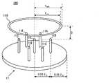
以下、本発明の実施形態を図面に基づいて説明する。図1は、本発明が適用されたアレーアンテナ装置であるアンテナ部1を備えた無線端末方向探知装置の構成図である。(First embodiment)
Hereinafter, embodiments of the present invention will be described with reference to the drawings. FIG. 1 is a configuration diagram of a wireless terminal direction finding device including an
この無線端末方向探知装置は、アンテナ部1、電力検出回路5、方向探知コンピュータ6を備えている。アンテナ部1は、電子制御導波器アレーアンテナ装置であり、詳しくは図2を用いて後述するが、1本の励振素子10と6本の非励振素子11A〜11Fとを備えている。これら励振素子10、非励振素子11A〜11Fは、接地導体17の上に、その接地導体17から絶縁された状態に設けられている。また、励振素子10、非励振素子11A〜11Fの外側には、それらの素子10、11A〜11Fをまとめて囲う導体円環板19が配置されている。 This wireless terminal direction finding device includes an
励振素子10の給電点は、同軸ケーブル20を介して電力検出回路5に接続されており、外部の無線端末から送信され励振素子10によって受信された電波を示す受信信号は電力検出回路5に供給される。 A feeding point of the
非励振素子11A〜11Fには、可変リアクタンス回路18A〜18Fがそれぞれ接続されている。この可変リアクタンス回路18は、電子制御導波器アレーアンテナ装置において一般的に用いられるものと同一の回路であり、たとえば、バイアス電圧が印加されることによってリアクタンス値が変化する可変リアクタンス素子(例えば可変容量ダイオード)を含む回路として構成される。この回路は、高周波的に接地導体17に接続され、方向探知コンピュータ6の後述する可変リアクタンス制御部61によってリアクタンス値が電子的に変化させられる。このリアクタンス値が変化させられることにより、アンテナ部1は方位角φが変化する。
電力検出回路5は、励振素子10から供給された受信信号の電力の大きさ(電力値)を検出する回路である。この電力検出回路5は、無線信号の電力を検出する種々の公知の回路を用いることができ、たとえばダイオード検波器を含む回路構成のものである。この電力検出回路5で検出された電力値を示す電力値信号は図示しないAD変換回路を介して方向探知コンピュータ6の方向探知部62に供給される。 The
方向探知コンピュータ6は、CPU、ROM、RAM等(いずれも図示せず)を備えており、CPUがRAMの一時記憶機能を利用しつつROMに記憶されているプログラムを実行することにより、可変リアクタンス制御部61および方向探知部62として機能する。 The
可変リアクタンス制御部61は、図示しないメモリに記憶されたデジタル電圧値を参照して、内蔵した6個のDA変換器(図示せず)を用いてそのデジタル電圧値をアナログのバイアス電圧値に変換し、このバイアス電圧値をリアクタンス値信号C11(θ)〜C16(θ)として各可変リアクタンス回路18A〜18Fに出力する。上記デジタル電圧値は、予め設定された複数の方位角(たとえば、0°から330°まで30°毎)にビームを形成する複数の指向性ビームパターンに対して記憶されている。可変リアクタンス制御部61は、リアクタンス値信号C11(θ)〜C16(θ)を切り替えることにより、指向性ビームパターンを複数の方位角に順次変化させる。なお、メモリに記憶されたデジタル電圧値は、実験に基づいて予め求められた値である。 The variable
方向探知部62は、電力検出回路5から供給される電力値と、その電力値の受信信号を受信したときの方位角とに基づいて無線端末の方向探知を行なう。たとえば、方位角に対する電力値の変化を示す電力値パターンを作成し、そのパターンにおいてピーク値を示す方位角を無線端末の方向に決定する。 The
図2は、アンテナ部1を拡大して示す図である。励振素子10および6本の非励振素子11A〜11Fはいずれも円柱形状であって接地導体17から垂直に突き出している。6本の非励振素子11A〜11Fの長さは互いに同一であり、また、励振素子10も非励振素子11と略同じ長さである。より詳しくは、励振素子10の、接地導体17の上面から素子上端までの長さをL(以下、励振素子長という)としたとき、非励振素子11の、接地導体17の上面から素子上端までの長さは、0.9L〜1.1Lの範囲で適宜設定される。なお、励振素子10の長さと非励振素子11の長さとの関係は、この形式の公知のアレーアンテナと同じである。 FIG. 2 is an enlarged view of the
上記励振素子長Lは約λ/4であり、詳しくは、0.78×(λ/4)<L<0.86×(λ/4)である。なお、λは、アンテナ部1が受信する電波の波長である。 The excitation element length L is about λ / 4. Specifically, 0.78 × (λ / 4) <L <0.86 × (λ / 4). Note that λ is the wavelength of the radio wave received by the
また、励振素子10は接地導体17の中心に配置される。一方、非励振素子11A〜11Fは、励振素子10を中心とする円周上に等間隔に設けられており、励振素子10と非励振素子11との間の距離(素子間距離r0とする)は、非励振素子11が導波器あるいは反射器として機能するようにするため、λ/4に設定されている。The
接地導体17は、励振素子10や非励振素子11A〜11Fに対して十分に大きい広さの円板形状部材であり、ここでは半径がλ/2とする。 The
アンテナ部1においてここまでに説明した構成は、公知の電子走査導波器アレーアンテナ装置と同じであり、本発明においても、公知の電子走査導波器アレーアンテナ装置と同様の種々の設計変更が可能である。本発明は、この公知の構成において、導体円環板19をさらに備えることに特徴がある。 The configuration described so far in the
導体円環板19は、導体性であり、形状は、円環形状、且つ、板状である。この導体円環板19は、励振素子10から見て、非励振素子11よりもさらに外側に、非励振素子11から離隔して設けられている。 The
また、この導体円環板19は、接地導体17と平行となっており、且つ、中心軸線は接地導体17の中心軸線と一致している。なお、この導体円環板19は、接地導体17、励振素子10、非励振素子11とともにこの導体円環板19を収容する図示しないアンテナ筐体に固定されている。 The conductor
ここで、図2に示すように、接地導体17の上面(導体円環板19側の面)と導体円環板19の下面との間の距離をd、導体円環板19の内半径をrin、外半径をroutとする。この距離dおよび半径rin、routが以下に示す(1)〜(8)のいずれかの条件を満たす場合、この導体円環板19があることにより、導体円環板19がない場合に比べて軸比が向上することをシミュレーションにより確認した。
1.0<d<0.24Lの場合
(1) r0<rin<0.35λ、 0.40λ≦rout≦0.74λ
(2) 0.35λ≦rin<rout≦0.74λ
2.0.24L≦d<0.35Lの場合
(3) r0<rin<0.35λ、 0.35λ≦rout≦0.74λ
(4) 0.35λ≦rin<rout≦0.74λ
3.0.35L≦d<0.43Lの場合
(5) r0<rin<0.30λ、 rin<rout≦0.74λ
(6) 0.30λ≦rin<0.35λ、 0.35λ≦rout≦0.74λ
(7) 0.35λ≦rin<rout≦0.74λ
4.0.43L≦d<1.00Lの場合
(8) r0<rin<rout≦0.74λHere, as shown in FIG. 2, the distance between the upper surface of the ground conductor 17 (the surface on the
When 1.0 <d <0.24L (1) r0 <rin <0.35λ, 0.40λ ≦ rout ≦ 0.74λ
(2) 0.35λ ≦ rin <rout ≦ 0.74λ
2. When 0.24L ≦ d <0.35L (3) r0 <rin <0.35λ, 0.35λ ≦ rout ≦ 0.74λ
(4) 0.35λ ≦ rin <rout ≦ 0.74λ
3. When 0.35L ≦ d <0.43L (5) r0 <rin <0.30λ, rin <rout ≦ 0.74λ
(6) 0.30λ ≦ rin <0.35λ, 0.35λ ≦ rout ≦ 0.74λ
(7) 0.35λ ≦ rin <rout ≦ 0.74λ
4.0 When 0.43L ≦ d <1.00L (8) r0 <rin <rout ≦ 0.74λ
なお、軸比とは、前述したように、主放射成分利得と、その主放射成分と直交する偏波の利得との比であり、アレーアンテナ装置では、垂直偏波が、受信の主放射成分となることが要求され、垂直偏波を受信の主放射成分としてみたとき、水平偏波が、主放射成分と直交する偏波である。 As described above, the axial ratio is the ratio between the main radiation component gain and the gain of the polarization orthogonal to the main radiation component. In the array antenna apparatus, the vertical polarization is the main radiation component of reception. When the vertical polarization is viewed as the main radiation component of reception, the horizontal polarization is a polarization orthogonal to the main radiation component.
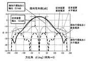
図3は、本実施形態のアレーアンテナ装置と、従来アレーアンテナ装置(導体円環板19がない以外は本実施形態のアレーアンテナ装置と同じ構成)の仰角=0における指向性利得を比較して示す図である。なお、図3では、本実施形態のアレーアンテナ装置は、図2において距離dが0.75L、外半径routが0.44λ、内半径rinが0.30λ、波長λが122.4mm(2.45GHz)、励振素子長L=0.83×(λ/4)、非励振素子の長さ=Lである。FIG. 3 shows a comparison of the directivity gain at an elevation angle = 0 between the array antenna apparatus of the present embodiment and the conventional array antenna apparatus (same configuration as the array antenna apparatus of the present embodiment except for the absence of the conductor ring plate 19). FIG. In FIG. 3, the array antenna apparatus of the present embodiment has a distance d of 0.75 L, an outer radius rout of 0.44λ, an inner radius rin of 0.30λ, and a wavelength λ of 122.4 mm (see FIG. 2). 2.45 GHz), excitation element length L = 0.83 × (λ / 4), and length of non-excitation element = L.
また、図3の利得は、コンピュータを用いたシミュレーションにより算出したものであり、シミュレーションにおいては、接地導体17、導体円環板19は、いずれも完全導体としており、厚さは、いずれも0.02mmとしている。ただし、接地導体17については表皮効果により、電流は表面にしか流れないため、20μm以上では特性に差は生じないことが知られている。同様に、導体円環板19についても、厚さはアンテナ特性に影響しないと考察している。また、材質についても、通常、アンテナの接地導体として用いられるものを導体円環板19についても用いれば、このシミュレーションとほぼ同一の結果になると考えられる。 Further, the gain in FIG. 3 is calculated by a simulation using a computer. In the simulation, the
この図3から分かるように、水平偏波指向性利得は、導体円環板19があることにより、従来アレーアンテナ装置に比較して全体的に低下している。これに対し、垂直偏波指向性利得は、導体円環板19の有無による利得の変化はほとんどない。よって、導体円環板19を備える本実施形態の装置の受信時の軸比は、従来アレーアンテナ装置よりも高くなる。具体的には、図3の例では、従来アレーアンテナ装置の軸比は15.6dBであるのに対して、導体円環板19がある場合の軸比は26.0dBとなっている。 As can be seen from FIG. 3, the horizontal polarization directivity gain is generally reduced as compared with the conventional array antenna apparatus due to the presence of the conductor
次に、前述の距離d、内半径rin、外半径routが上記(1)〜(8)の範囲であれば、従来アレーアンテナ装置よりも受信時の軸比が改善することをシミュレーション結果を用いて説明する。Next, if the distance d, the inner radius rin , and the outer radius rout are in the above ranges (1) to (8), the simulation result shows that the axial ratio during reception is improved as compared with the conventional array antenna apparatus. Will be described.
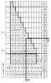
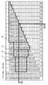
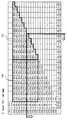
図4〜図16は、いずれも、導体円環板19の内半径rin、および外半径routを変化させつつシミュレーションにより算出した軸比(dB)である。軸比は、リアクタンス値を所望の方位角φとしたときのその方位角φにおける垂直偏波利得と、リアクタンス値を所望の方位角φとしたときの360°方位内の最大の水平偏波利得から算出している。なお、このシミュレーションにおいて、周波数は2.45GHz、すなわち、波長λは約122.4mmであり、励振素子長Lは25.5mm(≒0.83×(λ/4))、非励振素子長=Lである。4 to 16 are axial ratios (dB) calculated by simulation while changing the inner radius rin and the outer radius rout of the conductor
図4〜図16の違いは、導体円環板19と接地導体17との間の距離dである。各図には、シミュレーション条件における距離dが、ミリメートル単位と励振素子長Lに対する比率で示してある。また、各図において、その距離dの左側に示す数字は、請求項1における距離dの6つの範囲に対応する。そして、各図において、太線で囲んでいる範囲は、請求項1に記載した内半径rin、外半径routにより規定される範囲であり、その太線と引出線でつながっているかっこ内の数字は、請求項1における(1)〜(8)に対応する。The difference between FIGS. 4 to 16 is the distance d between the
図4〜図6は、距離dがそれぞれ、1mm(0.04L)、3mm(0.12L)、5mm(0.20L)であり、請求項1の「1.」の場合、すなわち、0<d<0.24Lに含まれる。図4〜図6は、それぞれ、この「1.」の範囲の最小距離付近のデータ、中間距離付近のデータ、最大距離付近のデータである。図4〜図6に太線で示す範囲はいずれも、従来アレーアンテナ装置の軸比15.6dBよりも大きい。よって、図4〜図6のシミュレーション結果より、請求項1の(1)、(2)で規定される範囲であれば、軸比が従来アレーアンテナ装置よりも大きくなることが分かる。 4 to 6, the distance d is 1 mm (0.04 L), 3 mm (0.12 L), and 5 mm (0.20 L), respectively. It is included in d <0.24L. 4 to 6 respectively show data near the minimum distance, data near the intermediate distance, and data near the maximum distance in the range of “1.”. The range indicated by the thick lines in FIGS. 4 to 6 is larger than the axial ratio of 15.6 dB of the conventional array antenna apparatus. Therefore, it can be seen from the simulation results of FIGS. 4 to 6 that the axial ratio is larger than that of the conventional array antenna apparatus within the range defined by (1) and (2) of
なお、図4〜図6における二重線は、接地導体17の半径を示している。よって、太線で示す範囲であって、且つ、二重線よりも矢印で示す方向である場合には、導体円環板19を設けても、アレーアンテナ装置は、径方向寸法が大きくならないので特に好ましい。 4 to 6 indicate the radius of the
図7、8は、距離dがそれぞれ、6mm(0.24L)、8mm(0.31L)であり、請求項1の「2.」の場合、すなわち、0.24L≦d<0.35Lの場合の最小距離のデータ、最大距離付近のデータである。太線で示す範囲はいずれも、従来アレーアンテナ装置の軸比15.6dBよりも大きい。よって、図7、図8のシミュレーション結果より、請求項1の(3)、(4)で規定される範囲であれば、軸比が従来アレーアンテナ装置よりも大きくなることが分かる。 7 and 8, the distances d are 6 mm (0.24 L) and 8 mm (0.31 L), respectively, and in the case of “2.” in
図9、10は、距離dがそれぞれ、9mm(0.35L)、10mm(0.39L)であり、請求項1の「3.」の場合、すなわち、0.35L≦d<0.43Lの場合の最小距離のデータ、最大距離付近のデータである。太線で示す(5)、(6)、(7)の範囲はいずれも、従来アレーアンテナ装置の軸比15.6dBよりも大きい。よって、図9、図10のシミュレーション結果より、請求項1の(5)、(6)、(7)で規定される範囲であれば、軸比が従来アレーアンテナ装置よりも大きくなることが分かる。もちろん、太線で示す範囲であって、且つ、二重線よりも矢印で示す方向が、径方向寸法が大きくならないので特に好ましい。 9 and 10, the distances d are 9 mm (0.35 L) and 10 mm (0.39 L), respectively, and in the case of “3.” in
図11〜図15は、距離dがそれぞれ、11mm(0.43L)、16mm(0.63L)、21mm(0.82L)、22mm(0.86L)、24mm(0.94L)であり、請求項1の「4.」の場合、すなわち、0.43L≦d<1.00Lに含まれる。また、図16は、距離dが26mm(1.02L)であり、請求項1の「4.」の場合の上限値をやや超えた距離である。 11 to 15, the distances d are 11 mm (0.43 L), 16 mm (0.63 L), 21 mm (0.82 L), 22 mm (0.86 L), and 24 mm (0.94 L), respectively. In case of “4.” in
つまり、図11、図16は、それぞれ、この「4.」の範囲の最小距離のデータ、最大距離付近のデータであり、図12〜図15は、この「4.」の範囲の中間距離のデータである。各図において太線で示す(8)の範囲はいずれも、従来アレーアンテナ装置の軸比15.6dBと同等以上である。よって、図11〜図16のシミュレーション結果より、請求項1の(8)で規定される範囲であれば、軸比が従来アレーアンテナ装置よりも大きくなることが分かる。もちろん、太線で示す範囲であって、且つ、二重線よりも矢印で示す方向が特に好ましい。 That is, FIGS. 11 and 16 show the minimum distance data in the range of “4.” and the data in the vicinity of the maximum distance, respectively, and FIGS. 12 to 15 show the intermediate distance in the range of “4.”. It is data. In each figure, the range indicated by the bold line (8) is equal to or greater than the axial ratio of 15.6 dB of the conventional array antenna apparatus. Therefore, it can be seen from the simulation results of FIGS. 11 to 16 that the axial ratio is larger than that of the conventional array antenna apparatus within the range defined by (8) of
以上、説明したように、接地導体17と平行であり、中心軸線が接地導体17の中心軸線と一致し、且つ、上記(1)〜(8)の何れかの条件を満たす導体円環板19を備えることで、従来アレーアンテナ装置に比較して受信時の軸比を改善することができる。 As described above, the conductor
しかも、上記(1)〜(8)のいずれにおいても、dは、励振素子長Lと同程度かそれよりも短いことから、導体円環板19を備えても、アレーアンテナ装置の高さ方向寸法はほとんど大きくならない。よって、装置の大型化を抑制しつつ、軸比を改善することができる。 In addition, in any of the above (1) to (8), d is approximately equal to or shorter than the excitation element length L. Therefore, even if the conductor
また、図4〜図16において、太線で示す範囲であって、且つ、二重線よりも矢印で示す方向である場合には、導体円環板19を設けても、アレーアンテナ装置は、径方向寸法も大きくならないので特に好ましい。 4 to 16, the array antenna device has a diameter even if the conductor
なお、軸比の観点では、従来アレーアンテナ装置の軸比15.6dBに対して3dBの差があれば顕著な差であると言える。よって、図4〜図16において、軸比が18.6dB以上である範囲が特に好ましいと言える。もちろん、軸比が18.6dBであって、導体円環板19の外半径routが接地導体17の半径よりも小さい範囲が最も好ましい。From the viewpoint of the axial ratio, if there is a difference of 3 dB with respect to the axial ratio of 15.6 dB of the conventional array antenna apparatus, it can be said that it is a significant difference. Therefore, in FIGS. 4 to 16, it can be said that the range in which the axial ratio is 18.6 dB or more is particularly preferable. Of course, it is most preferable that the axial ratio is 18.6 dB and the outer radius rout of the
(励振素子長Lの影響)
これまでに示した図4〜図16のデータは、L=0.83×(λ/4)=25.5mmにおけるデータであった。本発明者は、Lを変化させると軸比の変化が見られるものの、前述した(1)〜(8)の範囲であれば、アンテナとして機能する範囲でLを変化させても、軸比の変化は、従来よりも軸比が改善する範囲内であることを確認した。すなわち、前述した(1)〜(8)の範囲であれば、Lによらず、軸比改善効果があることを確認した。(Influence of excitation element length L)
The data shown in FIGS. 4 to 16 shown so far are data at L = 0.83 × (λ / 4) = 25.5 mm. Although the present inventor changes the axial ratio when L is changed, the axial ratio can be changed even if L is changed within the range of functioning as an antenna within the range of (1) to (8) described above. It was confirmed that the change was within a range where the axial ratio was improved as compared with the conventional case. That is, it was confirmed that there was an axial ratio improving effect regardless of L in the range of (1) to (8) described above.
図17は、アンテナとして機能する励振素子長Lの範囲を説明する図であり、図18〜図20は、励振素子長Lによらず軸比改善効果があることを確認したデータである。 FIG. 17 is a diagram for explaining the range of the excitation element length L that functions as an antenna, and FIGS. 18 to 20 are data that confirms that there is an effect of improving the axial ratio regardless of the excitation element length L.
図17には、実用上の周波数範囲から代表的な周波数として選択した3つの周波数(2400MHz、2450MHz、250MHz)において、励振素子長Lを変化させることにより正面利得がどのように変化するかを示している。なお、非励振素子長は常に励振素子長Lと同じ長さとしている。 FIG. 17 shows how the front gain changes by changing the excitation element length L at three frequencies (2400 MHz, 2450 MHz, and 250 MHz) selected as typical frequencies from the practical frequency range. ing. The non-excitation element length is always the same as the excitation element length L.
この図17において、網掛けした数値は、各周波数における正面利得のピーク値である。また、四角で囲んだ範囲は、正面利得がピーク値から1dBより少ない低下で済む範囲である。この四角で囲んだ範囲に対応する素子長Lをアンテナとして機能する素子長Lの範囲とする。 In FIG. 17, the shaded numerical values are the peak values of the front gain at each frequency. Further, the range surrounded by the square is a range in which the front gain can be reduced by less than 1 dB from the peak value. The element length L corresponding to the range enclosed by the square is defined as the range of the element length L that functions as an antenna.
図18〜図20は、いずれも、素子長Lを、アンテナとして機能する素子長Lの最小値付近(L=23.9mm)、中間値付近(L=25.5mm)、最大値付近(L=26.3mm)の3種に変化させて得た軸比のシミュレーション結果である。 In each of FIGS. 18 to 20, the element length L is set near the minimum value (L = 23.9 mm), the intermediate value (L = 25.5 mm), and the maximum value (L = 26.3 mm) is a simulation result of the axial ratio obtained by changing to three types.
図18、図19、図20の違いは、導体円環板19の高さdであり、図18はd=0.50L、図19はd=0.75L、図20はd=1.00Lである。これら図18〜図20を見ると分かるように、素子長Lが変化することにより軸比は変化するものの、図20の左上角部を除き、従来の軸比と同等以上の軸比となっていることが分かる。 The difference between FIG. 18, FIG. 19, and FIG. 20 is the height d of the
図20では、(A)、(B)、(C)ともに、表の左上角に、従来軸比と同程度あるいはわずかに劣る値も存在する。この理由は、本発明のアンテナ部1は、開放型アンテナであることによると考察している。詳しくは以下の通りである。 In FIG. 20, for both (A), (B), and (C), there is also a value that is the same as or slightly inferior to the conventional axial ratio in the upper left corner of the table. The reason is considered that the
一般に、開放型アンテナでは開放端が他の部材の影響を受けやすいことが知られている。そして、d=1.00Lのときは、素子先端の高さに導体円環板19が存在する。よって、素子10、11が導体円環板19の影響を最も受けやすい距離dであると言える。加えて、表の左上角部は、内半径Rinが小さいことから、径方向においても、導体円環板19は非励振素子11に近く、かつ、外半径Routが大きいことから、幅のある導体円環板19である。つまり、図20の表の左上角部は、素子10、11に最も近いところに、素子10、11に与える影響が大きい導体円環板19が存在している状況である。In general, it is known that the open end of an open antenna is easily affected by other members. When d = 1.00 L, the conductor
この距離d=1.00Lから導体円環板19が下方(dが小さくなる方向)に移動すれば、導体円環板19と素子先端との相互作用は低下する。よって、軸比は高くなると考察できる。この距離d=1.00Lにおいても、軸比は、従来とほぼ同等であることから、距離dが1.00Lよりも小さくなれば軸比は従来よりも向上すると考察できる。よって、d<1.00Lであれば請求項1の(8)の範囲で軸比改善効果があると言える。 If the conductor
なお、図18〜図20は、素子長L、すなわち、物理長を変化させたデータである。素子長Lを変化させるとアンテナの電気長が変化する。よって、アンテナとして機能する範囲で電気長を変化させても、前述した(1)〜(8)の範囲で、軸比改善効果があると言える。 18 to 20 show data in which the element length L, that is, the physical length is changed. When the element length L is changed, the electrical length of the antenna changes. Therefore, even if the electrical length is changed within the range of functioning as an antenna, it can be said that there is an effect of improving the axial ratio in the range of (1) to (8) described above.
(第2実施形態)
次に、第2実施形態を説明する。なお、以下の説明において、それまでに使用した符号と同一番号の符号を有する要素は、特に言及する場合を除き、それ以前の実施形態における同一符号の要素と同一である。また、構成の一部のみを説明している場合、構成の他の部分については先に説明した実施形態を適用することができる。(Second Embodiment)
Next, a second embodiment will be described. In the following description, elements having the same reference numerals as those used so far are the same as the elements having the same reference numerals in the previous embodiments unless otherwise specified. In addition, when only a part of the configuration is described, the embodiment described above can be applied to other parts of the configuration.
図21は、第2実施形態におけるアンテナ部100を拡大して示す図である。第2実施形態のアンテナ部100は、第1実施形態では励振素子10の上端と同程度の位置あるいは上端よりも下方(接地導体17側)に配置されていた導体円環板19に代えて、励振素子10の上端よりも上方に配置される導体円環板119を備える。その他の構成は第1実施形態と同じである。 FIG. 21 is an enlarged view of the
導体円環板119は、配置位置は第1実施形態の導体円環板19と異なるが、導体性である点および形状が円環形状かつ板状である点では第1実施形態の導体円環板19と同じである。 The
また、導体円環板119は、接地導体17と平行である点、中心軸線が接地導体17の中心軸線と一致している点も第1実施形態の導体円環板19と同じである。この導体円環板119は、接地導体17、励振素子10、非励振素子11とともにこの導体円環板119を収容する図示しないアンテナ筐体に固定されている。 The
図21に示すように、励振素子10の上端と導体円環板119の下面との間の距離をD、導体円環板119の内半径をrin、外半径をroutとする。この距離Dおよび半径rin、routが以下に示す(1)〜(19)のいずれかの条件を満たす場合、この導体円環板119があることにより、導体円環板119がない場合に比べて軸比が向上することをシミュレーションにより確認した。なお、λは第1実施形態と同じく、アンテナ部1が受信する電波の波長であり、この波長は電波の周波数により定まる自由空間波長である。
1.0≦D<0.03λの場合
(1) 0<rin<0.17λ、 0.34λ≦rout≦0.61λ
(2) 0.17λ≦rin<0.25λ、 0.30λ≦rout≦0.65λ
(3) 0.25λ≦rin<0.33λ、 rin<rout<0.65λ
(4) 0.33λ≦rin<rout≦0.74λ
2.0.03λ≦D<0.05λの場合
(5) 0<rin<0.21λ、 0.34λ≦rout≦0.61λ
(6) 0.21λ<rin<0.33λ、 0.30λ≦rout≦0.61λ
(7) 0.33λ≦rin<rout≦0.74λ
3.0.05λ≦D<0.07λの場合
(8) 0<rin<0.25λ、 0.38λ≦rout≦0.61λ
(9) 0.25λ≦rin<0.33λ、 0.34λ≦rout≦0.62λ
(10) 0.33λ≦rin<rout≦0.74λ
4.0.07λ≦D<0.14λの場合
(11) 0<rin<0.25λ、 0.34λ≦rout≦0.62λ
(12) 0.25λ≦rin<0.33λ、 0.34λ≦rout≦0.66λ
(13) 0.33λ≦rin<rout≦0.74λ
5.0.14λ≦D<0.23λの場合
(14) 0<rin<0.33λ、 0.34λ≦rout≦0.74λ
(15) 0.33λ≦rin<rout≦0.74λ
6.0.23λ≦D<0.24λの場合
(16) 0<rin<0.37λ、 0.34λ≦rout≦0.74λ
(17) 0.37λ≦rin≦0.49λ、 0.46λ≦rout≦0.74λ
7.0.24λ≦D<0.29λの場合
(18) 0<rin<0.37λ、 0.34λ≦rout≦0.66λ
(19) 0.33λ<rin≦0.49λ、 0.50λ≦rout≦0.66λAs shown in FIG. 21, it is assumed that the distance between the upper end of the
When 1.0 ≦ D <0.03λ (1) 0 <rin <0.17λ, 0.34λ ≦ rout ≦ 0.61λ
(2) 0.17λ ≦ rin <0.25λ, 0.30λ ≦ rout ≦ 0.65λ
(3) 0.25λ ≦ rin <0.33λ, rin <rout <0.65λ
(4) 0.33λ ≦ rin <rout ≦ 0.74λ
2. When 0.03λ ≦ D <0.05λ (5) 0 <rin <0.21λ, 0.34λ ≦ rout ≦ 0.61λ
(6) 0.21λ <rin <0.33λ, 0.30λ ≦ rout ≦ 0.61λ
(7) 0.33λ ≦ rin <rout ≦ 0.74λ
3. When 0.05λ ≦ D <0.07λ (8) 0 <rin <0.25λ, 0.38λ ≦ rout ≦ 0.61λ
(9) 0.25λ ≦ rin <0.33λ, 0.34λ ≦ rout ≦ 0.62λ
(10) 0.33λ ≦ rin <rout ≦ 0.74λ
4.0 When 0.07λ ≦ D <0.14λ (11) 0 <rin <0.25λ, 0.34λ ≦ rout ≦ 0.62λ
(12) 0.25λ ≦ rin <0.33λ, 0.34λ ≦ rout ≦ 0.66λ
(13) 0.33λ ≦ rin <rout ≦ 0.74λ
In the case of 5.0.14λ ≦ D <0.23λ (14) 0 <rin <0.33λ, 0.34λ ≦ rout ≦ 0.74λ
(15) 0.33λ ≦ rin <rout ≦ 0.74λ
6. When 0.23λ ≦ D <0.24λ (16) 0 <rin <0.37λ, 0.34λ ≦ rout ≦ 0.74λ
(17) 0.37λ ≦ rin ≦ 0.49λ, 0.46λ ≦ rout ≦ 0.74λ
7. When 0.24λ ≦ D <0.29λ (18) 0 <rin <0.37λ, 0.34λ ≦ rout ≦ 0.66λ
(19) 0.33λ <rin ≦ 0.49λ, 0.50λ ≦ rout ≦ 0.66λ
図22は、第2実施形態のアレーアンテナ装置と従来アレーアンテナ装置の仰角=0における指向性利得を比較して示す図である。なお、図22では、本実施形態のアレーアンテナ装置は、距離Dが0.03λ、外半径routが0.59λ、内半径rinが0.33λ、波長λが122.4mm(2.45GHz)、励振素子長L=0.83×(λ/4)、非励振素子の長さ=Lである。なお、この図22のグラフも、図3と同様、シミュレーションにより算出したものであり、接地導体17、導体円環板119はいずれも完全導体であり厚さは0.02mmとしている。FIG. 22 is a diagram showing a comparison of directivity gains at an elevation angle = 0 between the array antenna apparatus of the second embodiment and the conventional array antenna apparatus. In FIG. 22, the array antenna apparatus according to the present embodiment has a distance D of 0.03λ, an outer radius rout of 0.59λ, an inner radius rin of 0.33λ, and a wavelength λ of 122.4 mm (2.45 GHz). ), Excitation element length L = 0.83 × (λ / 4), and length of non-excitation element = L. The graph of FIG. 22 is also calculated by simulation in the same manner as FIG. 3, and both the
この図22から分かるように、水平偏波指向性利得は、導体円環板119があることにより、従来アレーアンテナ装置に比較して全体的に低下している。これに対し、垂直偏波指向性利得は、導体円環板119の有無による利得の変化はほとんどない。よって、導体円環板119を備える第2実施形態の装置の受信時の軸比は、従来アレーアンテナ装置よりも高くなる。具体的には、図22の例では、従来アレーアンテナ装置の軸比は15.6dBであるのに対して、導体円環板119がある場合の軸比は25.9dBとなっている。 As can be seen from FIG. 22, the horizontal polarization directivity gain is generally reduced as compared with the conventional array antenna apparatus due to the presence of the conductor
次に、前述の距離D、内半径rin、外半径routが上記(1)〜(19)の範囲であれば、従来アレーアンテナ装置よりも受信時の軸比が改善することをシミュレーション結果を用いて説明する。Next, if the above-mentioned distance D, inner radius rin , and outer radius rout are in the ranges (1) to (19), the simulation result shows that the axial ratio during reception is improved as compared with the conventional array antenna apparatus. Will be described.
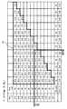
図23〜図39は、いずれも、導体円環板119の内半径rin、および外半径routを変化させつつシミュレーションにより算出した軸比(dB)である。軸比の算出方法は第1実施形態と同じである。また、このシミュレーションにおいて、周波数は2.45GHz、すなわち、波長λは約122.4mmであり、励振素子長Lは25.5mm(≒0.83×(λ/4))、非励振素子長=Lである。23 to 39 are axial ratios (dB) calculated by simulation while changing the inner radius rin and the outer radius rout of the conductor
図23〜図39の違いは、距離Dの範囲である。各図には、シミュレーション条件における距離Dが、ミリメートル単位と励振素子長Lに対する比率で示してある(ただし、ミリメートルについては励振素子長L(25.5mm)を加えた値である)。また、各図において、その距離Dの左側に示す数字は、請求項3における距離Dの7つの範囲に対応する。そして、各図において、太線で囲んでいる範囲は、請求項3に記載した内半径rin、外半径routにより規定される範囲であり、その太線と引出線でつながっているかっこ内の数字は、請求項3における(1)〜(19)に対応する。The difference between FIGS. 23 to 39 is the range of the distance D. In each figure, the distance D under the simulation conditions is shown as a unit of millimeter and a ratio to the excitation element length L (however, the millimeter is a value obtained by adding the excitation element length L (25.5 mm)). Moreover, in each figure, the number shown on the left side of the distance D corresponds to the seven ranges of the distance D in
図23〜25は、距離Dがそれぞれ、0.008λ(26.5mm)、0.016λ(27.5mm)、0.025λ(28.5mm)であり、請求項3の「1.」の場合、すなわち、0≦D<0.03λの場合の最小距離付近のデータ、中間距離付近のデータ、最大距離付近のデータである。太線で示す範囲はいずれも、従来アレーアンテナ装置の軸比15.6dBよりも大きい。よって、図23〜25のシミュレーション結果より、請求項3の(1)、(2)、(3)、(4)で規定される範囲であれば、軸比が従来アレーアンテナ装置よりも大きくなることが分かる。 23 to 25, the distances D are 0.008λ (26.5 mm), 0.016λ (27.5 mm), and 0.025λ (28.5 mm), respectively. That is, the data near the minimum distance, the data near the intermediate distance, and the data near the maximum distance when 0 ≦ D <0.03λ. The range indicated by the bold line is larger than the axial ratio of 15.6 dB of the conventional array antenna apparatus. Therefore, from the simulation results shown in FIGS. 23 to 25, the axial ratio is larger than that of the conventional array antenna apparatus within the range defined by (1), (2), (3), and (4) of
図26、27は、距離Dがそれぞれ、0.033λ(29.5mm)、0.041λ(30.5mm)であり、請求項3の「2.」の場合、すなわち、0.03λ≦D<0.05λの場合の最小距離付近のデータ、最大距離付近のデータである。太線で示す(5)、(6)、(7)の範囲はいずれも、従来アレーアンテナ装置の軸比15.6dBよりも大きい。よって、図26、図27のシミュレーション結果より、請求項3の(5)、(6)、(7)で規定される範囲も、軸比が従来アレーアンテナ装置よりも大きくなることが分かる。 26 and 27, the distances D are 0.033λ (29.5 mm) and 0.041λ (30.5 mm), respectively, and in the case of “2.” in
図28、29は、距離Dがそれぞれ、0.057λ(32.5mm)、0.065λ(33.5mm)であり、請求項3の「3.」の場合、すなわち、0.05λ≦D<0.07λの場合の最小距離付近のデータ、最大距離付近のデータである。太線で示す(8)、(9)、(10)の範囲はいずれも、従来アレーアンテナ装置の軸比15.6dBよりも大きい。よって、図28、図29のシミュレーション結果より、請求項3の(8)、(9)、(10)で規定される範囲も、軸比が従来アレーアンテナ装置よりも大きくなることが分かる。 28 and 29, the distances D are 0.057λ (32.5 mm) and 0.065λ (33.5 mm), respectively, and in the case of “3.” in FIG. 3, that is, 0.05λ ≦ D < Data near the minimum distance and data near the maximum distance in the case of 0.07λ. The ranges (8), (9), and (10) indicated by bold lines are all larger than the axial ratio of 15.6 dB of the conventional array antenna apparatus. Therefore, it can be seen from the simulation results of FIGS. 28 and 29 that the axial ratio of the ranges defined by (8), (9), and (10) of
図30〜32は、距離Dがそれぞれ、0.074λ(34.5mm)、0.10λ(37.5mm)、0.13λ(41.5mm)であり、請求項3の「4.」の場合、すなわち、0.07λ≦D<0.14λの場合の最小距離付近のデータ、中間距離付近のデータ、最大距離付近のデータである。太線で示す(11)、(12)、(13)の範囲はいずれも、従来アレーアンテナ装置の軸比15.6dBよりも大きい。よって、図30〜32のシミュレーション結果より、請求項3の(11)、(12)、(13)で規定される範囲も、軸比が従来アレーアンテナ装置よりも大きくなることが分かる。 30 to 32, the distances D are 0.074λ (34.5 mm), 0.10λ (37.5 mm), and 0.13λ (41.5 mm), respectively, in the case of “4.” in
図33〜35は、距離Dがそれぞれ、0.15λ(43.5mm)、0.19λ(48.5mm)、0.22λ(52.5mm)であり、請求項3の「5.」の場合、すなわち、0.14λ≦D<0.23λの場合の最小距離付近のデータ、中間距離付近のデータ、最大距離付近のデータである。太線で示す(14)、(15)の範囲はいずれも、従来アレーアンテナ装置の軸比15.6dBよりも大きい。よって、図33〜35のシミュレーション結果より、請求項3の(14)、(15)で規定される範囲も、軸比が従来アレーアンテナ装置よりも大きくなることが分かる。 In FIGS. 33 to 35, the distances D are 0.15λ (43.5 mm), 0.19λ (48.5 mm), and 0.22λ (52.5 mm), respectively. That is, the data near the minimum distance, the data near the intermediate distance, and the data near the maximum distance when 0.14λ ≦ D <0.23λ. The ranges of (14) and (15) indicated by bold lines are both larger than the axial ratio of 15.6 dB of the conventional array antenna apparatus. Therefore, it can be understood from the simulation results of FIGS. 33 to 35 that the axial ratio of the range defined by (14) and (15) of
図36、37は、距離Dがそれぞれ、0.23λ(53.5mm)、0.24λ(54.5mm)であり、請求項3の「6.」の場合、すなわち、0.23λ≦D<0.24λの場合の最小距離付近のデータ、最大距離付近のデータである。太線で示す(16)、(17)の範囲はいずれも、従来アレーアンテナ装置の軸比15.6dBよりも大きい。よって、図36、図37のシミュレーション結果より、請求項3の(16)、(17)で規定される範囲も、軸比が従来アレーアンテナ装置よりも大きくなることが分かる。 In FIGS. 36 and 37, the distances D are 0.23λ (53.5 mm) and 0.24λ (54.5 mm), respectively, in the case of “6.” in
図38、39は、距離Dがそれぞれ、0.25λ(55.5mm)、0.28λ(59.5mm)であり、請求項3の「7.」の場合、すなわち、0.24λ≦D<0.29λの場合の最小距離付近のデータ、最大距離付近のデータである。太線で示す(18)、(19)の範囲はいずれも、従来アレーアンテナ装置の軸比15.6dBよりも大きい。よって、図38、図39のシミュレーション結果より、請求項3の(18)、(19)で規定される範囲も、軸比が従来アレーアンテナ装置よりも大きくなることが分かる。 38 and 39, the distances D are 0.25λ (55.5 mm) and 0.28λ (59.5 mm), respectively, and in the case of “7.” in
以上、説明したように、接地導体17と平行であり、中心軸線が接地導体17の中心軸線と一致し、且つ、上記(1)〜(19)の何れかの条件を満たす導体円環板119を備えることで、従来アレーアンテナ装置に比較して受信時の軸比を改善することができる。 As described above, the conductor
しかも、導体円環板119は励振素子10の上方に配置している。すなわち、励振素子10の上方を活用して受信時の軸比を改善しているので、径方向の大型化が抑制できる。特に、図23〜39において太線で示す範囲であって、且つ、二重線よりも矢印で示す方向である場合には、導体円環板119を設けても、アレーアンテナ装置は径方向には大型化しない。 In addition, the
さらに、導体円環板119は接地導体17とは別構成であることから、接地導体17のみを大きくするよりも、アレーアンテナ装置の大型化を抑制しつつ受信時の軸比を改善することができる。 Furthermore, since the
なお、軸比の観点では、従来アレーアンテナ装置の軸比15.6dBに対して3dBの差があれば顕著な差であると言える。よって、図23〜図39において、軸比が18.6dB以上である範囲が特に好ましいと言える。もちろん、軸比が18.6dBであって、導体円環板19の外半径routが接地導体17の半径よりも小さい範囲がより好ましい。From the viewpoint of the axial ratio, if there is a difference of 3 dB with respect to the axial ratio of 15.6 dB of the conventional array antenna apparatus, it can be said that it is a significant difference. Therefore, in FIGS. 23 to 39, it can be said that the range in which the axial ratio is 18.6 dB or more is particularly preferable. Of course, it is more preferable that the axial ratio is 18.6 dB and the outer radius rout of the conductor
以上、本発明の実施形態を説明したが、本発明は上述の実施形態に限定されるものではなく、要旨を逸脱しない範囲内で種々変更して実施することができる。 As mentioned above, although embodiment of this invention was described, this invention is not limited to the above-mentioned embodiment, It can implement in various changes within the range which does not deviate from a summary.
1 アンテナ部、 5 電力検出回路、 6 方向探知コンピュータ、 10 励振素子、 11 非励振素子、 17 接地導体、 18 可変リアクタンス回路、 19 導体円環板、 20 同軸ケーブル、 61 可変リアクタンス制御部、 62 方向探知部 100 アンテナ部、 119 導体円環板DESCRIPTION OF
Claims (4)
Translated fromJapanese前記接地導体の中心に、その接地導体から絶縁された状態で設けられ、無線信号を受信する励振素子と、
前記接地導体上にその接地導体から絶縁された状態で設けられた複数の非励振素子と、
各非励振素子にそれぞれ接続された複数の可変リアクタンス素子と、を備え、
可変リアクタンス素子のリアクタンス値が変化することにより、前記複数の非励振素子が導波器あるいは反射器として機能するように、それら複数の非励振素子は、前記励振素子から所定の素子間距離だけ離隔して配置されているアレーアンテナ装置であって、
前記接地導体に対して前記励振素子および非励振素子側に導体円環板が配置されており、且つ、その導体円環板は、
前記接地導体と平行であり、
中心軸線が前記接地導体の中心軸線と一致し、
前記接地導体の上面と導体円環板の下面との間の距離d、導体円環板の内半径rin、外半径routが、前記励振素子の長さをL、アレーアンテナ装置が受信する電波の波長をλとしたとき、下記(1)〜(8)のいずれかの条件を満たしていることを特徴とするアレーアンテナ装置。
1.0<d<0.24Lの場合
(1) 素子間距離<rin<0.35λ、 0.40λ≦rout≦0.74λ
(2) 0.35λ≦rin<rout≦0.74λ
2.0.24L≦d<0.35Lの場合
(3) 素子間距離<rin<0.35λ、 0.35λ≦rout≦0.74λ
(4) 0.35λ≦rin<rout≦0.74λ
3.0.35L≦d<0.43Lの場合
(5) 素子間距離<rin<0.30λ、 rin<rout≦0.74λ
(6) 0.30λ≦rin<0.35λ、 0.35λ≦rout≦0.74λ
(7) 0.35λ≦rin<rout≦0.74λ
4.0.43L≦d<1.00Lの場合
(8) 素子間距離<rin<rout≦0.74λA circular ground conductor;
An excitation element provided at the center of the ground conductor in a state insulated from the ground conductor and receiving a radio signal;
A plurality of parasitic elements provided on the ground conductor in a state of being insulated from the ground conductor;
A plurality of variable reactance elements respectively connected to each non-excitation element,
The plurality of non-excitation elements are separated from the excitation elements by a predetermined inter-element distance so that the reactance values of the variable reactance elements change so that the plurality of non-excitation elements function as a director or a reflector. An array antenna device arranged as
A conductor ring plate is disposed on the excitation element and non-excitation element side with respect to the ground conductor, and the conductor ring plate is
Parallel to the ground conductor;
The central axis coincides with the central axis of the ground conductor;
The distance d between the upper surface of the ground conductor and the lower surface of the conductor ring plate, the inner radius rin and the outer radius rout of the conductor ring plate are L, and the array antenna apparatus receives the length of the excitation element. An array antenna apparatus characterized by satisfying any of the following conditions (1) to (8), where λ is the wavelength of the radio wave.
When 1.0 <d <0.24L (1) Inter-element distance <rin <0.35λ, 0.40λ ≦ rout ≦ 0.74λ
(2) 0.35λ ≦ rin <rout ≦ 0.74λ
2. In the case of 0.24L ≦ d <0.35L (3) Inter-element distance <rin <0.35λ, 0.35λ ≦ rout ≦ 0.74λ
(4) 0.35λ ≦ rin <rout ≦ 0.74λ
3. When 0.35L ≦ d <0.43L (5) Distance between elements <rin <0.30λ, rin <rout ≦ 0.74λ
(6) 0.30λ ≦ rin <0.35λ, 0.35λ ≦ rout ≦ 0.74λ
(7) 0.35λ ≦ rin <rout ≦ 0.74λ
4. In the case of 0.43L ≦ d <1.00L (8) Distance between elements <rin <rout ≦ 0.74λ
前記(1)〜(8)のいずれかの条件において、外半径routの上限値を前記接地導体の半径に置き換えた条件を満たしていることを特徴とするアレーアンテナ装置。In claim 1,
The array antenna apparatus according to any one of the above (1) to (8), wherein a condition in which an upper limit value of an outer radius rout is replaced with a radius of the ground conductor is satisfied.
前記接地導体の中心に、その接地導体から絶縁された状態で設けられ、無線信号を受信する励振素子と、
前記接地導体上にその接地導体から絶縁された状態で設けられた複数の非励振素子と、
各非励振素子にそれぞれ接続された複数の可変リアクタンス素子と、を備え、
可変リアクタンス素子のリアクタンス値が変化することにより、前記複数の非励振素子が導波器あるいは反射器として機能するように、それら複数の非励振素子は、前記励振素子から所定の素子間距離だけ離隔して配置されているアレーアンテナ装置であって、
前記接地導体に対して前記励振素子および非励振素子側に導体円環板が配置されており、且つ、その導体円環板は、
前記接地導体と平行であり、
中心軸線が前記接地導体の中心軸線と一致し、
前記励振素子の上端と前記導体円環板の下面との間の距離D、導体円環板の内半径rin、外半径routが、アレーアンテナ装置が受信する電波の波長をλとしたとき、下記(1)〜(19)のいずれかの条件を満たしていることを特徴とするアレーアンテナ装置。1.0≦D<0.03λの場合
(1) 0<rin<0.17λ、 0.34λ≦rout≦0.61λ
(2) 0.17λ≦rin<0.25λ、 0.30λ≦rout≦0.65λ
(3) 0.25λ≦rin<0.33λ、 rin<rout<0.65λ
(4) 0.33λ≦rin<rout≦0.74λ
2.0.03λ≦D<0.05λの場合
(5) 0<rin<0.21λ、 0.34λ≦rout≦0.61λ
(6) 0.21λ<rin<0.33λ、 0.30λ≦rout≦0.61λ
(7) 0.33λ≦rin<rout≦0.74λ
3.0.05λ≦D<0.07λの場合
(8) 0<rin<0.25λ、 0.38λ≦rout≦0.61λ
(9) 0.25λ≦rin<0.33λ、 0.34λ≦rout≦0.62λ
(10) 0.33λ≦rin<rout≦0.74λ
4.0.07λ≦D<0.14λの場合
(11) 0<rin<0.25λ、 0.34λ≦rout≦0.62λ
(12) 0.25λ≦rin<0.33λ、 0.34λ≦rout≦0.66λ
(13) 0.33λ≦rin<rout≦0.74λ
5.0.14λ≦D<0.23λの場合
(14) 0<rin<0.33λ、 0.34λ≦rout≦0.74λ
(15) 0.33λ≦rin<rout≦0.74λ
6.0.23λ≦D<0.24λの場合
(16) 0<rin<0.37λ、 0.34λ≦rout≦0.74λ
(17) 0.37λ≦rin≦0.49λ、 0.46λ≦rout≦0.74λ
7.0.24λ≦D<0.29λの場合
(18) 0<rin<0.37λ、 0.34λ≦rout≦0.66λ
(19) 0.33λ<rin≦0.49λ、 0.50λ≦rout≦0.66λA circular ground conductor;
An excitation element provided at the center of the ground conductor in a state insulated from the ground conductor and receiving a radio signal;
A plurality of parasitic elements provided on the ground conductor in a state of being insulated from the ground conductor;
A plurality of variable reactance elements respectively connected to each non-excitation element,
The plurality of non-excitation elements are separated from the excitation elements by a predetermined inter-element distance so that the reactance values of the variable reactance elements change so that the plurality of non-excitation elements function as a director or a reflector. An array antenna device arranged as
A conductor ring plate is disposed on the excitation element and non-excitation element side with respect to the ground conductor, and the conductor ring plate is
Parallel to the ground conductor;
The central axis coincides with the central axis of the ground conductor;
When the distance D between the upper end of the excitation element and the lower surface of the conductor ring plate, the inner radius rin and the outer radius rout of the conductor ring plate are λ, the wavelength of the radio wave received by the array antenna device is λ An array antenna apparatus satisfying any of the following conditions (1) to (19): When 1.0 ≦ D <0.03λ (1) 0 <rin <0.17λ, 0.34λ ≦ rout ≦ 0.61λ
(2) 0.17λ ≦ rin <0.25λ, 0.30λ ≦ rout ≦ 0.65λ
(3) 0.25λ ≦ rin <0.33λ, rin <rout <0.65λ
(4) 0.33λ ≦ rin <rout ≦ 0.74λ
2. When 0.03λ ≦ D <0.05λ (5) 0 <rin <0.21λ, 0.34λ ≦ rout ≦ 0.61λ
(6) 0.21λ <rin <0.33λ, 0.30λ ≦ rout ≦ 0.61λ
(7) 0.33λ ≦ rin <rout ≦ 0.74λ
3. When 0.05λ ≦ D <0.07λ (8) 0 <rin <0.25λ, 0.38λ ≦ rout ≦ 0.61λ
(9) 0.25λ ≦ rin <0.33λ, 0.34λ ≦ rout ≦ 0.62λ
(10) 0.33λ ≦ rin <rout ≦ 0.74λ
4.0 When 0.07λ ≦ D <0.14λ (11) 0 <rin <0.25λ, 0.34λ ≦ rout ≦ 0.62λ
(12) 0.25λ ≦ rin <0.33λ, 0.34λ ≦ rout ≦ 0.66λ
(13) 0.33λ ≦ rin <rout ≦ 0.74λ
In the case of 5.0.14λ ≦ D <0.23λ (14) 0 <rin <0.33λ, 0.34λ ≦ rout ≦ 0.74λ
(15) 0.33λ ≦ rin <rout ≦ 0.74λ
6. When 0.23λ ≦ D <0.24λ (16) 0 <rin <0.37λ, 0.34λ ≦ rout ≦ 0.74λ
(17) 0.37λ ≦ rin ≦ 0.49λ, 0.46λ ≦ rout ≦ 0.74λ
7. When 0.24λ ≦ D <0.29λ (18) 0 <rin <0.37λ, 0.34λ ≦ rout ≦ 0.66λ
(19) 0.33λ <rin ≦ 0.49λ, 0.50λ ≦ rout ≦ 0.66λ
前記(1)〜(19)のいずれかの条件において、外半径routの上限値を前記接地導体の半径に置き換えた条件を満たしていることを特徴とするアレーアンテナ装置。In claim 3,
The array antenna apparatus according to any one of (1) to (19), wherein the condition that the upper limit value of the outer radius rout is replaced with the radius of the ground conductor is satisfied.
Priority Applications (1)
| Application Number | Priority Date | Filing Date | Title |
|---|---|---|---|
| JP2013045599AJP2014082736A (en) | 2012-03-29 | 2013-03-07 | Array antenna device |
Applications Claiming Priority (5)
| Application Number | Priority Date | Filing Date | Title |
|---|---|---|---|
| JP2012077235 | 2012-03-29 | ||
| JP2012077235 | 2012-03-29 | ||
| JP2012214979 | 2012-09-27 | ||
| JP2012214979 | 2012-09-27 | ||
| JP2013045599AJP2014082736A (en) | 2012-03-29 | 2013-03-07 | Array antenna device |
Publications (1)
| Publication Number | Publication Date |
|---|---|
| JP2014082736Atrue JP2014082736A (en) | 2014-05-08 |
Family
ID=50786519
Family Applications (1)
| Application Number | Title | Priority Date | Filing Date |
|---|---|---|---|
| JP2013045599APendingJP2014082736A (en) | 2012-03-29 | 2013-03-07 | Array antenna device |
Country Status (1)
| Country | Link |
|---|---|
| JP (1) | JP2014082736A (en) |
Cited By (1)
| Publication number | Priority date | Publication date | Assignee | Title |
|---|---|---|---|---|
| EP4178039A1 (en)* | 2021-11-04 | 2023-05-10 | Politechnika Gdanska | Electronically steered beam antenna of espar type |
- 2013
- 2013-03-07JPJP2013045599Apatent/JP2014082736A/enactivePending
Cited By (1)
| Publication number | Priority date | Publication date | Assignee | Title |
|---|---|---|---|---|
| EP4178039A1 (en)* | 2021-11-04 | 2023-05-10 | Politechnika Gdanska | Electronically steered beam antenna of espar type |
Similar Documents
| Publication | Publication Date | Title |
|---|---|---|
| US11145973B2 (en) | Planar end-fire pattern reconfigurable antenna | |
| JP5709805B2 (en) | Vertically polarized antenna | |
| KR102482836B1 (en) | Electronic device with antenna device | |
| JP6528748B2 (en) | Antenna device | |
| WO2001091231A1 (en) | Directional switch antenna device | |
| JP7565392B2 (en) | Antenna Device | |
| JP5686192B2 (en) | Antenna device | |
| KR20130125361A (en) | Smart antenna for wireless communications | |
| US9837724B2 (en) | Antenna system | |
| WO2000069022A1 (en) | Circular-polarized antenna | |
| US20190081400A1 (en) | Antenna Structure | |
| JP5413103B2 (en) | Antenna device | |
| US8963774B1 (en) | Adaptive nulling for parasitic array antennas | |
| Lin et al. | A novel beam-switching array antenna using series-fed slots with PIN diodes | |
| US10923826B2 (en) | Double helical antenna | |
| Baik et al. | Switchable printed Yagi‐Uda antenna with pattern reconfiguration | |
| Parchin et al. | A beam-steerable antenna array with radiation beam reconfigurability for 5G smartphones | |
| Lim | Design of a multidirectional, high-gain compact Yagi antenna | |
| JP2014082736A (en) | Array antenna device | |
| JP2011087241A (en) | Antenna, and array antenna | |
| JP4276142B2 (en) | Traveling wave antenna | |
| JP5673472B2 (en) | Array antenna device | |
| JP5652182B2 (en) | Antenna device | |
| Qin et al. | A high-gain beam-steering quasi-yagi antenna | |
| JP4297852B2 (en) | Directional variable antenna |