JP2014078599A - Power conversion device - Google Patents
Power conversion deviceDownload PDFInfo
- Publication number
- JP2014078599A JP2014078599AJP2012225375AJP2012225375AJP2014078599AJP 2014078599 AJP2014078599 AJP 2014078599AJP 2012225375 AJP2012225375 AJP 2012225375AJP 2012225375 AJP2012225375 AJP 2012225375AJP 2014078599 AJP2014078599 AJP 2014078599A
- Authority
- JP
- Japan
- Prior art keywords
- power conversion
- refrigerant
- semiconductor modules
- frame
- end side
- Prior art date
- Legal status (The legal status is an assumption and is not a legal conclusion. Google has not performed a legal analysis and makes no representation as to the accuracy of the status listed.)
- Pending
Links
- 238000006243chemical reactionMethods0.000titleclaimsabstractdescription35
- 239000004065semiconductorSubstances0.000claimsabstractdescription64
- 238000001816coolingMethods0.000claimsabstractdescription43
- 239000002826coolantSubstances0.000claimsabstractdescription33
- 239000003507refrigerantSubstances0.000claimsdescription60
- 238000007599dischargingMethods0.000claims2
- 238000003475laminationMethods0.000abstractdescription4
- 230000000694effectsEffects0.000description4
- 230000002195synergetic effectEffects0.000description4
- 230000005669field effectEffects0.000description1
- 238000005549size reductionMethods0.000description1
Images


Classifications
- H—ELECTRICITY
- H05—ELECTRIC TECHNIQUES NOT OTHERWISE PROVIDED FOR
- H05K—PRINTED CIRCUITS; CASINGS OR CONSTRUCTIONAL DETAILS OF ELECTRIC APPARATUS; MANUFACTURE OF ASSEMBLAGES OF ELECTRICAL COMPONENTS
- H05K7/00—Constructional details common to different types of electric apparatus
- H05K7/20—Modifications to facilitate cooling, ventilating, or heating
- H05K7/2089—Modifications to facilitate cooling, ventilating, or heating for power electronics, e.g. for inverters for controlling motor
- H05K7/20927—Liquid coolant without phase change
- H—ELECTRICITY
- H01—ELECTRIC ELEMENTS
- H01L—SEMICONDUCTOR DEVICES NOT COVERED BY CLASS H10
- H01L23/00—Details of semiconductor or other solid state devices
- H01L23/34—Arrangements for cooling, heating, ventilating or temperature compensation ; Temperature sensing arrangements
- H01L23/46—Arrangements for cooling, heating, ventilating or temperature compensation ; Temperature sensing arrangements involving the transfer of heat by flowing fluids
- H01L23/473—Arrangements for cooling, heating, ventilating or temperature compensation ; Temperature sensing arrangements involving the transfer of heat by flowing fluids by flowing liquids
- H—ELECTRICITY
- H01—ELECTRIC ELEMENTS
- H01L—SEMICONDUCTOR DEVICES NOT COVERED BY CLASS H10
- H01L23/00—Details of semiconductor or other solid state devices
- H01L23/34—Arrangements for cooling, heating, ventilating or temperature compensation ; Temperature sensing arrangements
- H01L23/40—Mountings or securing means for detachable cooling or heating arrangements ; fixed by friction, plugs or springs
- H01L23/4006—Mountings or securing means for detachable cooling or heating arrangements ; fixed by friction, plugs or springs with bolts or screws
- H01L23/4012—Mountings or securing means for detachable cooling or heating arrangements ; fixed by friction, plugs or springs with bolts or screws for stacked arrangements of a plurality of semiconductor devices
- H—ELECTRICITY
- H01—ELECTRIC ELEMENTS
- H01L—SEMICONDUCTOR DEVICES NOT COVERED BY CLASS H10
- H01L2924/00—Indexing scheme for arrangements or methods for connecting or disconnecting semiconductor or solid-state bodies as covered by H01L24/00
- H01L2924/0001—Technical content checked by a classifier
- H01L2924/0002—Not covered by any one of groups H01L24/00, H01L24/00 and H01L2224/00
Landscapes
- Engineering & Computer Science (AREA)
- Microelectronics & Electronic Packaging (AREA)
- Physics & Mathematics (AREA)
- Thermal Sciences (AREA)
- Condensed Matter Physics & Semiconductors (AREA)
- General Physics & Mathematics (AREA)
- Computer Hardware Design (AREA)
- Power Engineering (AREA)
- Cooling Or The Like Of Semiconductors Or Solid State Devices (AREA)
- Inverter Devices (AREA)
Abstract
Description
Translated fromJapanese本発明は、半導体モジュールと冷却器とを有する電力変換装置に関する。 The present invention relates to a power conversion device having a semiconductor module and a cooler.
例えば、電気自動車やハイブリッド自動車等には、インバータ等の電力変換装置が搭載されている。該電力変換装置は、その電力変換回路を構成する半導体モジュールとこれを冷却する冷却器とを備えており、高出力かつ小型のものが望まれている。 For example, an electric vehicle, a hybrid vehicle, and the like are equipped with a power conversion device such as an inverter. The power conversion device includes a semiconductor module that constitutes the power conversion circuit and a cooler that cools the semiconductor module, and a high-output and small-sized device is desired.
特許文献1には、半導体モジュールと冷却器の冷媒流路とが交互に積層され、半導体モジュールを両主面から冷却可能に構成された電力変換装置が開示されている。特許文献1に記載された電力変換装置は、冷却性能を向上させて半導体モジュールからの発熱を効率よく除去することにより、高出力化を図ったものである。 Patent Document 1 discloses a power conversion device in which semiconductor modules and refrigerant flow paths of a cooler are alternately stacked so that the semiconductor module can be cooled from both main surfaces. The power conversion device described in Patent Document 1 is intended to increase the output by improving the cooling performance and efficiently removing the heat generated from the semiconductor module.
ところで、特許文献1に記載の電力変換装置を含め、従来の電力変換装置は、冷却器に冷却媒体を循環させるためにポンプを使用しており、冷却媒体を循環させる際にポンプにかかる負荷を低減することが求められている。そのため、電力変換装置とポンプとを接続する外部配管の内径をできるだけ大きくして冷却媒体の流通抵抗を小さくする設計が一般的であった。これに伴い、冷却器の冷媒導排管等に外部配管と適合するものを用いる必要があったため、冷却器の小型化には限界があった。 By the way, the conventional power conversion device including the power conversion device described in Patent Document 1 uses a pump to circulate the cooling medium in the cooler, and a load applied to the pump when the cooling medium is circulated. There is a need to reduce it. For this reason, it has been common to design the external pipe connecting the power converter and the pump as large as possible to reduce the flow resistance of the cooling medium. In connection with this, since it was necessary to use what was compatible with external piping for the refrigerant | coolant conducting / exhausting pipe | tube of a cooler, there existed a limit in size reduction of a cooler.
本発明は、上記の背景に鑑みてなされたもので、冷却性能に優れ、小型化の容易な電力変換装置を提供しようとするものである。 The present invention has been made in view of the above-described background, and an object of the present invention is to provide a power converter that has excellent cooling performance and can be easily downsized.
本発明の一態様は、電力変換回路の一部を構成する複数の半導体モジュールと、
該複数の半導体モジュールを冷却する複数の冷媒流路を有する冷却器と、
上記半導体モジュールと上記冷却器とを保持するフレームとを有し、
上記複数の半導体モジュールと上記複数の冷媒流路とは互いに積層されて積層体を構成しており、
上記冷却器は、上記積層方向の端部に配された上記冷媒流路を基端として上記積層方向に向けて上記フレームの外まで延伸形成された、冷却媒体を導排出する一対の冷媒導排管を有し、
上記一対の冷媒導排管のうち少なくとも一方の冷媒導排管は、上記フレームの内側に配される基端側管部が、上記フレームの外側に配される先端側管部よりも外径が小さいことを特徴とする電力変換装置にある(請求項1)。One embodiment of the present invention includes a plurality of semiconductor modules that form part of a power conversion circuit;
A cooler having a plurality of refrigerant flow paths for cooling the plurality of semiconductor modules;
A frame for holding the semiconductor module and the cooler;
The plurality of semiconductor modules and the plurality of refrigerant flow paths are stacked together to form a stacked body,
The cooler includes a pair of refrigerant guides and discharges that guide and discharge the cooling medium that is extended to the outside of the frame in the stacking direction with the coolant channel disposed at an end in the stacking direction as a base end. Has a tube,
At least one of the pair of refrigerant guide / exhaust pipes has a proximal end side pipe portion arranged on the inner side of the frame and an outer diameter larger than a distal end side pipe portion arranged on the outer side of the frame. It is in the power converter device characterized by being small (Claim 1).
上記電力変換装置は、上記一対の冷媒導排管のうち少なくとも一方の冷媒導排管における上記基端側管部が、上記先端側管部よりも外径が小さくなるよう構成されている。そのため、上記フレームの内側における上記冷媒導排管の占有体積を低減することができ、上記冷媒流路の流路方向における上記フレームの寸法を低減することが容易となる。その結果、上記電力変換装置を上記流路方向に小型化することが容易となる。 The power converter is configured such that the proximal end side pipe portion of at least one of the pair of refrigerant guide / exhaust tubes has a smaller outer diameter than the distal end side tube portion. Therefore, the occupied volume of the refrigerant guide / exhaust pipe inside the frame can be reduced, and the size of the frame in the flow path direction of the refrigerant flow path can be easily reduced. As a result, it becomes easy to miniaturize the power converter in the direction of the flow path.
また、上記電力変換装置の上記流路方向における寸法を増大させることなく上記先端側管部の外径を上記基端側管部の外径よりも大きくできるため、冷却器内部に流通する冷却媒体の量を多くしやすくなる。その結果、上記電力変換装置は、冷却性能に優れたものとなる。 In addition, since the outer diameter of the distal-end-side tube portion can be made larger than the outer diameter of the proximal-end-side tube portion without increasing the size of the power conversion device in the flow path direction, a cooling medium that circulates inside the cooler It becomes easy to increase the amount of. As a result, the power converter is excellent in cooling performance.
以上のごとく、上記態様によれば、冷却性能に優れ、小型化の容易な電力変換装置を提供することができる。 As described above, according to the above aspect, it is possible to provide a power conversion device that has excellent cooling performance and can be easily miniaturized.
上記電力変換装置において、上記複数の半導体モジュールは、隣り合う上記冷媒流路の間に1つずつ配されているとともに、上記積層方向に一列に配列されていてもよい(請求項2)。この場合には、隣り合う上記冷媒流路の間に複数の半導体モジュールが配される場合に比べて、隣り合う上記冷媒流路の間において半導体モジュールより発生する熱量の合計が小さくなる。また、隣り合う上記冷媒流路の間に複数の半導体モジュールが配される場合に比べて、各々の半導体モジュールを冷却する冷却媒体の温度を均一にしやすくなる。これらの各々の作用効果または両者の相乗効果により、上記電力変換装置は、半導体モジュールの冷却を効率よく行うことができ、冷却性能をより向上させることができる。 In the power converter, the plurality of semiconductor modules may be arranged one by one between the adjacent refrigerant flow paths, and may be arranged in a line in the stacking direction (Claim 2). In this case, the total amount of heat generated from the semiconductor modules between the adjacent refrigerant flow paths is smaller than when a plurality of semiconductor modules are arranged between the adjacent refrigerant flow paths. In addition, compared to the case where a plurality of semiconductor modules are arranged between the adjacent refrigerant flow paths, the temperature of the cooling medium that cools each semiconductor module can be made uniform. By each of these functions and effects, or the synergistic effect of the two, the power conversion device can efficiently cool the semiconductor module and can further improve the cooling performance.
また、上述のように複数の半導体モジュールを配置する場合には、隣り合う冷媒流路の間において発生する熱量が小さくなる。これにより、半導体モジュールの冷却を行うことが容易となるため、上記基端側管部の外径をより小さくすることができる。さらに、半導体モジュールが流路方向に複数配列されなくなるので、これらの相乗効果により、上記電力変換装置の流路方向における寸法の更なる低減が可能となる。 Further, when a plurality of semiconductor modules are arranged as described above, the amount of heat generated between adjacent refrigerant flow paths is reduced. Thereby, since it becomes easy to cool a semiconductor module, the outer diameter of the said base end side pipe part can be made smaller. Furthermore, since a plurality of semiconductor modules are not arranged in the flow path direction, the synergistic effect of these allows further reduction of the dimensions of the power converter in the flow path direction.
また、上記フレームは、上記積層方向と上記冷媒流路の流路方向である幅方向との双方と直交する高さ方向に立設された複数のボスを有し、該複数のボスは、上記複数の半導体モジュールの動作を制御する制御基板を締結可能に構成されており、該複数のボスのうち少なくとも一対のボスは、上記一対の冷媒導排管の上記基端側管部に対して上記幅方向の外側に隣接して配されていてもよい(請求項3)。この場合には、上記一対の冷媒導排管の上記基端側管部よりも上記幅方向の外側に生じる上記フレームのデッドスペースを、上記ボスを配設するためのスペースとして有効に活用することができる。また、上述のごとくボスを配設することにより、上記制御基板の締結箇所を4隅になるべく近づけることが可能となる。これにより、上記制御基板を安定して固定することが容易となる。 Further, the frame has a plurality of bosses erected in a height direction perpendicular to both the stacking direction and the width direction that is the flow path direction of the refrigerant flow path, and the plurality of bosses are The control board which controls operation of a plurality of semiconductor modules is constituted so that fastening is possible, and at least a pair of bosses among the plurality of bosses are the above-mentioned to the base end side pipe part of the above-mentioned pair of refrigerant guide pipes It may be arranged adjacent to the outside in the width direction (Claim 3). In this case, the dead space of the frame generated outside the base end side pipe portion of the pair of refrigerant guide and exhaust pipes in the width direction is effectively utilized as a space for arranging the boss. Can do. Further, by arranging the boss as described above, the fastening locations of the control board can be brought as close to the four corners as possible. Thereby, it becomes easy to fix the control board stably.
(実施例1)
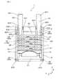
上記電力変換装置の実施例を、図1〜図3を用いて説明する。図1に示すように、電力変換装置1は、電力変換回路の一部を構成する複数の半導体モジュール10と、複数の半導体モジュール10を冷却する冷媒流路を構成する複数の冷却管21を有する冷却器2と、半導体モジュール10と冷却器2とを保持するフレーム3とを有している。また、複数の半導体モジュール10と複数の冷却管21とは互いに積層されて積層体11を構成している。Example 1
An embodiment of the power conversion device will be described with reference to FIGS. As shown in FIG. 1, the power conversion device 1 includes a plurality of
冷却器2は、積層体11の積層方向の端部に配された冷却管21を基端として積層方向に向けてフレーム3の外まで延伸形成された、冷却媒体を導排出する一対の冷媒導排管20を有している。そして、一対の冷媒導排管20は、フレーム3の内側に配される基端側管部200が、フレーム3の外側に配される先端側管部201よりも外径が小さくなるように形成されている。 The
以下において、積層体11の積層方向を「積層方向X」といい、積層方向Xと直交する冷媒流路の流路方向を「幅方向Y」という。また、積層方向Xと幅方向Yとの双方と直交する方向を「高さ方向Z」という。 In the following, the stacking direction of the
半導体モジュール10と冷却器2とは、図1に示すように、これらを四方から囲むフレーム3に保持されている。フレーム3の積層方向Xにおける一方の壁部30には一対の切り欠き開口部300が形成されており、一対の冷媒導排管20が切り欠き開口部300からフレーム3の外方に突出している。また、一対の切り欠き開口部300は、後述する冷媒導排管20の中間管部202を高さ方向Zに支持する支持部301を有しており、図には示さない固定クランプと支持部301との間に中間管部202を狭持可能に構成されている。 As shown in FIG. 1, the
また、図1に示すように、フレーム3は、積層方向Xと幅方向Yとの双方と直交する高さ方向Zに立設された4箇所のボス32(32a、32b、32c、32d)を有している。これらのボス32は、図2及び図3に示すように、複数の半導体モジュール10の動作を制御する制御基板14をボルト320により締結可能に構成されている。図1に示すように、4箇所のボス32のうち一対のボス32a、32bは、一対の冷媒導排管20の基端側管部200に対して幅方向Yの外側に隣接して配されている。また、他の一対のボス32c、32dは、フレーム3の積層方向Xにおける他方の壁部31側の2箇所の角部310にそれぞれ配されている。 Further, as shown in FIG. 1, the
一対の冷媒導排管20は、図1及び図3に示すように、積層方向Xにおける一方の壁部30側に配された冷却管21を基端として、フレーム3の外方に向けて延伸されている。また、一対の冷媒導排管20は、基端側管部200から積層方向Xに向けて延伸されつつ2段階に拡径されており、延伸方向(積層方向X)の先端部が先端側管部201を構成している。つまり、基端側管部200と先端側管部201の間には、両者の中間の外径を有する中間管部202が形成されており、基端側管部200と中間管部202との境界部分及び中間管部202と先端側管部201の境界部分の各々にテーパ状の段部203が形成されている。 As shown in FIGS. 1 and 3, the pair of refrigerant guide /
冷却器2は、図1に示すように、内部に冷却媒体を流通させる複数の冷却管21を積層方向Xにおいて所定の間隔を設けて並べて配置すると共に、隣り合う冷却管21同士を、その長手方向(幅方向Y)の両端部において連結管22によって連結している。そして、積層方向Xの一端に配置された冷却管21における長手方向の両端部に一対の冷媒導排管20の基端側管部200が接続されている。なお、本例において、連結管22の外径は基端側管部200の外径と略同一である。 As shown in FIG. 1, the
半導体モジュール10は、略直方体状の本体部100と、半導体モジュール10の動作を制御する制御端子101と、半導体モジュール10に電力を入出力する主端子(図示略)とを有している。制御端子101と主端子とは、それぞれ本体部100から互いに反対方向に突出している。本例においては、制御端子101は高さ方向Zの制御基板14が配される方向へ向けて突出しており、制御端子101と制御基板14とが電気的に接続可能に構成されている。また、本体部100には、IGBT(Insulated Gate Bipolar Transistor)やMOSFET(Metal-Oxide-Semiconductor Field Effect Transistor)等からなるスイッチング素子が1個ずつ内蔵されている。 The
複数の半導体モジュール10は、図1に示すように、隣り合う冷却管21の間に1つずつ配されているとともに、積層方向Xに一列に配列されている。そして、半導体モジュール10は、その両主面から一対の冷却管21によって挟持されている。これにより、複数の冷却管21と複数の半導体モジュール10とが交互に積層され、積層体11を構成している。また、積層方向Xに隣り合う半導体モジュール10は、制御端子101が幅方向Yにずれた状態で配置されている。 As shown in FIG. 1, the plurality of
上述のように構成された冷却器2において、一方の冷媒導排管20から導入された冷却媒体は、連結管22を適宜通り、各冷却管21に分配されると共にその長手方向に流通する。そして、各冷却管21を流れる間に、冷却媒体は半導体モジュール10との間で熱交換を行う。熱交換により温度上昇した冷却媒体は、下流側の連結管22を適宜通り、他方の冷媒導排管20に導かれ、冷却器2から排出される。 In the
また、複数の冷却管21と複数の半導体モジュール10との積層体11は、図1に示すように、積層方向Xの冷媒導排管20が接続されている側と反対側からバネ部材12によって積層方向Xに押圧されている。すなわち、フレーム3における切り欠き開口部300を有する一方の壁部30に積層方向Xの一端に配された冷却管21が接触し、フレーム3における他方の壁部31と積層体11の他端に配された冷却管21との間に、積層方向Xに広がる方向に付勢されたバネ部材12が配置されている。バネ部材12と冷却管21との間には、冷却管21の変形を防止するための当接板13が配置されている。 Moreover, as shown in FIG. 1, the
次に、本例の作用効果について説明する。電力変換装置1は、一対の冷媒導排管20のうち少なくとも一方の冷媒導排管20における基端側管部200が、先端側管部201よりも外径が小さくなるよう構成されている。そのため、フレーム3の内側における冷媒導排管20の占有体積を低減することができ、冷媒流路の流路方向(幅方向Y)におけるフレーム3の寸法を低減することが容易となる。その結果、電力変換装置1を幅方向Yに小型化することが容易となる。 Next, the function and effect of this example will be described. The power conversion device 1 is configured such that the proximal end
また、電力変換装置1の幅方向Yにおける寸法を増大させることなく先端側管部201の外径を基端側管部200の外径よりも大きくできるため、冷却器2内部に流通する冷却媒体の量を多くしやすくなる。その結果、電力変換装置1は、冷却性能に優れたものとなる。 Further, since the outer diameter of the distal end
また、複数の半導体モジュール10は、隣り合う冷却管21の間に1つずつ配されているとともに、積層方向Xに一列に配列されている。そのため、隣り合う冷却管21の間に複数の半導体モジュール10が配される場合に比べて、隣り合う冷却管21の間において半導体モジュール10より発生する熱量の合計が小さくなる。また、隣り合う冷却管21の間に複数の半導体モジュール10が配される場合に比べて、各々の半導体モジュール10を冷却する冷却媒体の温度を均一にしやすくなる。これらの各々の作用効果または両者の相乗効果により、電力変換装置1は、半導体モジュール10の冷却を効率よく行うことができ、冷却性能をより向上させることができる。 The plurality of
また、隣り合う冷却管21の間において発生する熱量が小さくなるため、半導体モジュール10の冷却が容易となり、基端側管部200の外径をより小さくすることができる。さらに、半導体モジュール10が流路方向(幅方向Y)に複数配列されなくなるので、これらの相乗効果により、電力変換装置1の幅方向Yにおける寸法の更なる低減が可能となる。 Further, since the amount of heat generated between the
また、フレーム3は、高さ方向Zに立設された複数のボス32を有し、複数のボス32は、複数の半導体モジュール10の動作を制御する制御基板14を締結可能に構成されており、複数のボス32のうち少なくとも一対のボス32は、一対の冷媒導排管20の基端側管部200に対して幅方向Yの外側に隣接して配されている。そのため、一対の冷媒導排管20の基端側管部200よりも幅方向Yの外側に生じるフレーム3のデッドスペースを、ボス32を配設するためのスペースとして有効に活用することができる。また、上述のごとくボス32を配設することにより、制御基板14の締結箇所を4隅になるべく近づけることが可能となる。これにより、制御基板14を安定して固定することが容易となる。 The
以上のごとく、本例によれば、冷却性能に優れ、小型化の容易な電力変換装置を提供することができる。 As described above, according to this example, it is possible to provide a power converter that has excellent cooling performance and can be easily downsized.
(実施例2)
本例は、実施例1における電力変換装置1の半導体モジュール10の配置を変更した例である。本例の電力変換装置102は、図4に示すように、互いに隣り合う冷却管21の間に、2つの半導体モジュール10が幅方向Yに互いに並んで配されている。そして、複数の半導体モジュール10は、積層方向Xに向けて2列に配列されている。(Example 2)
This example is an example in which the arrangement of the
また、本例においては、フレーム3に設けられた4箇所のボス32のうち、積層方向Xにおける一方の壁部30側に配された一対のボス32a、32bが、一対の冷媒導排管20の基端側管部200に対して幅方向Yの内側に隣接して配されている。その他は実施例1と同様である。なお、図4において用いた符号のうち、実施例1において用いた符号と同一の符号のものは、特に示さない限り実施例1と同様の構成要素等を表す。 Further, in this example, of the four
本例のように、隣り合う冷却管21の間に複数の半導体モジュール10が配設されている場合であっても、一方の冷媒導排管20における基端側管部200が、先端側管部201よりも外径が小さくなるよう構成されていれば、上述のように、冷媒流路の流路方向(幅方向Y)におけるフレーム3の寸法を低減することが容易となり、電力変換装置102を幅方向Yに小型化することが容易となる。 Even in the case where a plurality of
また、電力変換装置102の幅方向Yにおける寸法を増大させることなく先端側管部201の外径を基端側管部200の外径よりも大きくできるため、冷却器2内部に流通する冷却媒体の量を多くしやすくなる。その結果、電力変換装置102は、冷却性能に優れたものとなる。 In addition, since the outer diameter of the distal end
(実施例3)
本例は、実施例1における電力変換装置1の一対の冷媒導排管20(20a、20b)のうち、一方の冷媒導排管20aのみに基端側管部200よりも外径の大きい先端側管部201を形成した例である。本例の電力変換装置103は、図5に示すように、一方の冷媒導排管20aの先端側管部201が、実施例1と同様に基端側管部200よりも外径が大きくなるよう構成されている。また、他方の冷媒導排管20bは、基端側管部200と先端側管部204とが同一の外径となるよう構成されている。(Example 3)
In this example, of the pair of refrigerant guiding / exhausting pipes 20 (20a, 20b) of the power conversion apparatus 1 according to the first embodiment, only one of the refrigerant guiding /
本例の電力変換装置1は、例えば図5に示すように、他方の冷媒導排管20bの先端側管部204に冷媒導排管20bと外部配管とを接続するための接続アダプタ23を装着して用いられる。接続アダプタ23は、円筒状のパイプの中央部が略直角方向に屈曲されており、一方の開口端230に冷媒導排管20bの先端側管部204が挿入される。そして、外部配管と接続される他方の開口端231は、幅方向Yに向けて開口するように配される。その他は実施例1と同様である。なお、図5において用いた符号のうち、実施例1において用いた符号と同一の符号のものは、特に示さない限り実施例1と同様の構成要素等を表す。 For example, as shown in FIG. 5, the power conversion device 1 of this example is equipped with a
本例のように、一方の冷媒導排管20aのみに基端側管部200よりも外径の大きい先端側管部201を形成していれば、実施例1と同様の作用効果を奏することができる。なお、本例の電力変換装置において、冷却器2への冷却媒体の導入は、一方の冷媒導排管20aより行ってもよく、他方の冷媒導排管20bから行ってもよい。また、接続アダプタ23における他方の開口端231の向きは特に限定されず、高さ方向Zに向いていてもよい。 As in this example, if the distal end
また、実施例1〜3においては、冷媒流路を冷却管21によって形成し、冷却管21を半導体モジュール10に接触させた例を示したが、冷媒流路の態様はこれに限定されるものではない。例えば、冷媒流路を半導体モジュールと一体に形成し、半導体モジュールに冷却媒体を直接接触させて冷却させる構成も可能である。 Moreover, in Examples 1-3, although the coolant flow path was formed with the cooling
また、本例においては、バネ部材12を積層体11に対して他方の壁部31側に配したが、これに限るものではなく、一対の冷媒導排管20を設けた側に配してもよい。すなわち、例えば、一対の冷媒導排管20の間にバネ部材12を配し、積層体11を他方の壁部31側に向けて押圧させてもよい。 Further, in this example, the
1、102、103 電力変換装置
10 半導体モジュール
11 積層体
14 制御基板
2 冷却器
20 冷媒導排管
200 基端側管部
201 先端側管部
21 冷却管
3 フレーム
32 ボスDESCRIPTION OF
Claims (3)
Translated fromJapanese該複数の半導体モジュール(10)を冷却する複数の冷媒流路(21)を有する冷却器(2)と、
上記半導体モジュール(10)と上記冷却器(2)とを保持するフレーム(3)とを有し、
上記複数の半導体モジュール(10)と上記複数の冷媒流路(21)とは互いに積層されて積層体(11)を構成しており、
上記冷却器(2)は、上記積層方向の端部に配された上記冷媒流路(21)を基端として上記積層方向に向けて上記フレーム(3)の外まで延伸形成された、冷却媒体を導排出する一対の冷媒導排管(20)を有し、
上記一対の冷媒導排管(20)のうち少なくとも一方の冷媒導排管(20)は、上記フレーム(3)の内側に配される基端側管部(200)が、上記フレーム(3)の外側に配される先端側管部(201)よりも外径が小さいことを特徴とする電力変換装置(1、102、103)。A plurality of semiconductor modules (10) constituting a part of the power conversion circuit;
A cooler (2) having a plurality of refrigerant channels (21) for cooling the plurality of semiconductor modules (10);
A frame (3) for holding the semiconductor module (10) and the cooler (2);
The plurality of semiconductor modules (10) and the plurality of refrigerant flow paths (21) are stacked on each other to form a stacked body (11).
The cooling device (2) is a cooling medium that is formed to extend out of the frame (3) in the stacking direction with the refrigerant flow path (21) disposed at the end in the stacking direction as a base end. A pair of refrigerant guiding and discharging pipes (20) for guiding and discharging
At least one refrigerant guide / exhaust pipe (20) of the pair of refrigerant guide / exhaust pipes (20) has a base end side pipe portion (200) arranged on the inner side of the frame (3). The power converter (1, 102, 103) characterized in that the outer diameter is smaller than that of the distal end side pipe portion (201) disposed outside the tube.
Priority Applications (2)
| Application Number | Priority Date | Filing Date | Title |
|---|---|---|---|
| JP2012225375AJP2014078599A (en) | 2012-10-10 | 2012-10-10 | Power conversion device |
| US14/050,787US20140098496A1 (en) | 2012-10-10 | 2013-10-10 | Power conversion apparatus including semiconductor modules and cooler |
Applications Claiming Priority (1)
| Application Number | Priority Date | Filing Date | Title |
|---|---|---|---|
| JP2012225375AJP2014078599A (en) | 2012-10-10 | 2012-10-10 | Power conversion device |
Publications (1)
| Publication Number | Publication Date |
|---|---|
| JP2014078599Atrue JP2014078599A (en) | 2014-05-01 |
Family
ID=50432503
Family Applications (1)
| Application Number | Title | Priority Date | Filing Date |
|---|---|---|---|
| JP2012225375APendingJP2014078599A (en) | 2012-10-10 | 2012-10-10 | Power conversion device |
Country Status (2)
| Country | Link |
|---|---|
| US (1) | US20140098496A1 (en) |
| JP (1) | JP2014078599A (en) |
Families Citing this family (10)
| Publication number | Priority date | Publication date | Assignee | Title |
|---|---|---|---|---|
| EP2808988A4 (en)* | 2012-01-23 | 2015-11-25 | Toyota Motor Co Ltd | ELECTRIC POWER CONVERTING APPARATUS AND METHOD OF MANUFACTURING THE SAME |
| JP5655846B2 (en)* | 2012-12-04 | 2015-01-21 | 株式会社デンソー | Power converter |
| JP6197769B2 (en)* | 2014-09-12 | 2017-09-20 | 株式会社デンソー | Power converter and manufacturing method thereof |
| JP2016063641A (en)* | 2014-09-18 | 2016-04-25 | 株式会社デンソー | Power converter |
| JP6344340B2 (en)* | 2014-09-23 | 2018-06-20 | 株式会社デンソー | COOLER MODULE AND METHOD FOR MANUFACTURING COOLER MODULE |
| KR101653453B1 (en)* | 2014-11-03 | 2016-09-09 | 현대모비스 주식회사 | Cooling system for cooling both sides of power semiconductor |
| EP3206468B1 (en)* | 2016-02-15 | 2018-12-26 | Siemens Aktiengesellschaft | Converter with an intermediate d.c. circuit |
| JP6596398B2 (en)* | 2016-08-29 | 2019-10-23 | 本田技研工業株式会社 | Power converter |
| US9955613B2 (en)* | 2016-09-13 | 2018-04-24 | Denso International America, Inc. | Cooler and power electronic module having the same |
| JP7087638B2 (en)* | 2018-04-27 | 2022-06-21 | 株式会社デンソー | Power converter |
Citations (6)
| Publication number | Priority date | Publication date | Assignee | Title |
|---|---|---|---|---|
| JP2006210605A (en)* | 2005-01-27 | 2006-08-10 | Toyota Motor Corp | Semiconductor device and load driving device |
| JP2009094257A (en)* | 2007-10-08 | 2009-04-30 | Denso Corp | Power conversion device |
| JP2009254189A (en)* | 2008-04-09 | 2009-10-29 | Denso Corp | Power conversion apparatus |
| JP2011165922A (en)* | 2010-02-10 | 2011-08-25 | Denso Corp | Power conversion device |
| JP2011181687A (en)* | 2010-03-01 | 2011-09-15 | Denso Corp | Power converter |
| JP2011239623A (en)* | 2010-05-13 | 2011-11-24 | Denso Corp | Power conversion apparatus and manufacturing method thereof |
Family Cites Families (20)
| Publication number | Priority date | Publication date | Assignee | Title |
|---|---|---|---|---|
| DE1914790A1 (en)* | 1969-03-22 | 1970-10-01 | Siemens Ag | Liquid-cooled assembly with disc cells |
| US3864607A (en)* | 1972-03-16 | 1975-02-04 | Programmed Power | Stackable heat sink assembly |
| DE3133485A1 (en)* | 1980-09-15 | 1982-05-06 | Peter 2563 Ipsach Herren | LIQUID-COOLED ELECTRICAL ASSEMBLY |
| SE441047B (en)* | 1983-10-06 | 1985-09-02 | Asea Ab | Semi-conductor valve for high voltage with voltage divider sections including resistance |
| US5469331A (en)* | 1994-04-07 | 1995-11-21 | Conway; Harry E. | Cooling system for modular power supply device |
| EP2244289B1 (en)* | 2000-04-19 | 2014-03-26 | Denso Corporation | Coolant cooled type semiconductor device |
| JP4089595B2 (en)* | 2002-12-16 | 2008-05-28 | 株式会社デンソー | Refrigerant cooling type double-sided cooling semiconductor device |
| US7245493B2 (en)* | 2003-08-06 | 2007-07-17 | Denso Corporation | Cooler for cooling electric part |
| WO2005020276A2 (en)* | 2003-08-21 | 2005-03-03 | Denso Corporation | Power converter and semiconductor device mounting structure |
| DE102004059963A1 (en)* | 2003-12-18 | 2005-08-11 | Denso Corp., Kariya | Simply assembled radiator |
| JP2005332863A (en)* | 2004-05-18 | 2005-12-02 | Denso Corp | Power stack |
| JP4284625B2 (en)* | 2005-06-22 | 2009-06-24 | 株式会社デンソー | Three-phase inverter device |
| JP4506848B2 (en)* | 2008-02-08 | 2010-07-21 | 株式会社デンソー | Semiconductor module |
| JP5423654B2 (en)* | 2010-02-05 | 2014-02-19 | 株式会社デンソー | Power converter |
| JP5327195B2 (en)* | 2010-02-05 | 2013-10-30 | 株式会社デンソー | Power converter |
| JP4924750B2 (en)* | 2010-02-05 | 2012-04-25 | 株式会社デンソー | Power converter |
| JP5423655B2 (en)* | 2010-02-05 | 2014-02-19 | 株式会社デンソー | Power converter |
| JP5488565B2 (en)* | 2011-03-29 | 2014-05-14 | 株式会社デンソー | Power converter |
| JP5344013B2 (en)* | 2011-09-06 | 2013-11-20 | 株式会社デンソー | Power converter |
| JP5370448B2 (en)* | 2011-09-19 | 2013-12-18 | 株式会社デンソー | Power converter |
- 2012
- 2012-10-10JPJP2012225375Apatent/JP2014078599A/enactivePending
- 2013
- 2013-10-10USUS14/050,787patent/US20140098496A1/ennot_activeAbandoned
Patent Citations (6)
| Publication number | Priority date | Publication date | Assignee | Title |
|---|---|---|---|---|
| JP2006210605A (en)* | 2005-01-27 | 2006-08-10 | Toyota Motor Corp | Semiconductor device and load driving device |
| JP2009094257A (en)* | 2007-10-08 | 2009-04-30 | Denso Corp | Power conversion device |
| JP2009254189A (en)* | 2008-04-09 | 2009-10-29 | Denso Corp | Power conversion apparatus |
| JP2011165922A (en)* | 2010-02-10 | 2011-08-25 | Denso Corp | Power conversion device |
| JP2011181687A (en)* | 2010-03-01 | 2011-09-15 | Denso Corp | Power converter |
| JP2011239623A (en)* | 2010-05-13 | 2011-11-24 | Denso Corp | Power conversion apparatus and manufacturing method thereof |
Also Published As
| Publication number | Publication date |
|---|---|
| US20140098496A1 (en) | 2014-04-10 |
Similar Documents
| Publication | Publication Date | Title |
|---|---|---|
| JP2014078599A (en) | Power conversion device | |
| KR101653453B1 (en) | Cooling system for cooling both sides of power semiconductor | |
| JP2019118164A (en) | Power conversion system | |
| US8736041B2 (en) | Power converter | |
| JP6136760B2 (en) | Power converter | |
| JP2012069892A (en) | Semiconductor cooler | |
| JP2012210022A (en) | Electric power conversion apparatus | |
| JP5983340B2 (en) | Power converter | |
| JP5712750B2 (en) | Power converter | |
| US10548246B2 (en) | Electrical power converter | |
| JP2019221048A (en) | Electric power conversion device | |
| JP2016063641A (en) | Power converter | |
| JP2013090408A (en) | Electric power conversion device | |
| JP2013074721A (en) | Power conversion device | |
| JP6102641B2 (en) | Stacked cooler | |
| JP2017011922A (en) | Power conversion device | |
| JP2015070682A (en) | Power converter | |
| CN111699623B (en) | Electronic component with cooler and inverter | |
| JP2016063595A (en) | Power conversion apparatus | |
| JP2009194038A (en) | Cooler and power converting device using the same | |
| JP5999028B2 (en) | Power converter | |
| JP2013059155A (en) | Electric power conversion apparatus | |
| JP2011254679A (en) | Power conversion apparatus | |
| JP5810825B2 (en) | Power converter and manufacturing method thereof | |
| JP6088903B2 (en) | Power converter |
Legal Events
| Date | Code | Title | Description |
|---|---|---|---|
| A621 | Written request for application examination | Free format text:JAPANESE INTERMEDIATE CODE: A621 Effective date:20140131 | |
| A977 | Report on retrieval | Free format text:JAPANESE INTERMEDIATE CODE: A971007 Effective date:20140818 | |
| A131 | Notification of reasons for refusal | Free format text:JAPANESE INTERMEDIATE CODE: A131 Effective date:20140902 | |
| A521 | Written amendment | Free format text:JAPANESE INTERMEDIATE CODE: A523 Effective date:20141029 | |
| A02 | Decision of refusal | Free format text:JAPANESE INTERMEDIATE CODE: A02 Effective date:20150203 | |
| A521 | Written amendment | Free format text:JAPANESE INTERMEDIATE CODE: A523 Effective date:20150422 | |
| A911 | Transfer to examiner for re-examination before appeal (zenchi) | Free format text:JAPANESE INTERMEDIATE CODE: A911 Effective date:20150430 | |
| A912 | Re-examination (zenchi) completed and case transferred to appeal board | Free format text:JAPANESE INTERMEDIATE CODE: A912 Effective date:20150703 |