JP2014072120A - Organic el device, method for manufacturing organic el device, and electronic apparatus - Google Patents
Organic el device, method for manufacturing organic el device, and electronic apparatusDownload PDFInfo
- Publication number
- JP2014072120A JP2014072120AJP2012219135AJP2012219135AJP2014072120AJP 2014072120 AJP2014072120 AJP 2014072120AJP 2012219135 AJP2012219135 AJP 2012219135AJP 2012219135 AJP2012219135 AJP 2012219135AJP 2014072120 AJP2014072120 AJP 2014072120A
- Authority
- JP
- Japan
- Prior art keywords
- light emitting
- emitting layer
- sub
- pixel
- anode
- Prior art date
- Legal status (The legal status is an assumption and is not a legal conclusion. Google has not performed a legal analysis and makes no representation as to the accuracy of the status listed.)
- Pending
Links
- 238000000034methodMethods0.000titleclaimsabstractdescription63
- 238000004519manufacturing processMethods0.000titleabstractdescription12
- 238000007740vapor depositionMethods0.000claimsabstractdescription30
- 239000000463materialSubstances0.000claimsdescription85
- 238000002347injectionMethods0.000claimsdescription66
- 239000007924injectionSubstances0.000claimsdescription66
- 238000000576coating methodMethods0.000claimsdescription41
- 239000000470constituentSubstances0.000claimsdescription22
- 239000003086colorantSubstances0.000claimsdescription10
- 150000004032porphyrinsChemical class0.000claimsdescription7
- 238000001704evaporationMethods0.000claimsdescription4
- IEQIEDJGQAUEQZ-UHFFFAOYSA-NphthalocyanineChemical compoundN1C(N=C2C3=CC=CC=C3C(N=C3C4=CC=CC=C4C(=N4)N3)=N2)=C(C=CC=C2)C2=C1N=C1C2=CC=CC=C2C4=N1IEQIEDJGQAUEQZ-UHFFFAOYSA-N0.000claimsdescription4
- 239000010410layerSubstances0.000description332
- 239000010408filmSubstances0.000description66
- 239000000758substrateSubstances0.000description27
- 238000005192partitionMethods0.000description22
- 230000005525hole transportEffects0.000description21
- 239000002346layers by functionSubstances0.000description19
- 239000007788liquidSubstances0.000description16
- 239000000126substanceSubstances0.000description15
- 239000011229interlayerSubstances0.000description14
- -1N, N-diphenylaminoChemical group0.000description11
- 239000004065semiconductorSubstances0.000description9
- 230000008569processEffects0.000description8
- VYPSYNLAJGMNEJ-UHFFFAOYSA-Nsilicon dioxideInorganic materialsO=[Si]=OVYPSYNLAJGMNEJ-UHFFFAOYSA-N0.000description7
- 229920001467poly(styrenesulfonates)Polymers0.000description6
- 229910052814silicon oxideInorganic materials0.000description6
- 239000002904solventSubstances0.000description6
- 229910004298SiO 2Inorganic materials0.000description5
- 239000007769metal materialSubstances0.000description5
- 239000000203mixtureSubstances0.000description5
- 230000004048modificationEffects0.000description5
- 238000012986modificationMethods0.000description5
- 238000000059patterningMethods0.000description5
- 230000001681protective effectEffects0.000description5
- 238000007789sealingMethods0.000description5
- 239000000243solutionSubstances0.000description5
- 229920000178Acrylic resinPolymers0.000description4
- 239000004925Acrylic resinSubstances0.000description4
- 229910052783alkali metalInorganic materials0.000description4
- 229910052784alkaline earth metalInorganic materials0.000description4
- 229910052782aluminiumInorganic materials0.000description4
- 239000002585baseSubstances0.000description4
- 229910052761rare earth metalInorganic materials0.000description4
- 229920001609Poly(3,4-ethylenedioxythiophene)Polymers0.000description3
- 229910006404SnO 2Inorganic materials0.000description3
- 229910045601alloyInorganic materials0.000description3
- 239000000956alloySubstances0.000description3
- 230000008901benefitEffects0.000description3
- 239000003990capacitorSubstances0.000description3
- 150000001805chlorine compoundsChemical class0.000description3
- 150000004696coordination complexChemical class0.000description3
- 229910052802copperInorganic materials0.000description3
- 239000010949copperSubstances0.000description3
- 239000002612dispersion mediumSubstances0.000description3
- 150000002222fluorine compoundsChemical class0.000description3
- 229910052737goldInorganic materials0.000description3
- 239000011159matrix materialSubstances0.000description3
- 229910052751metalInorganic materials0.000description3
- 239000002184metalSubstances0.000description3
- 238000002156mixingMethods0.000description3
- 229920000767polyanilinePolymers0.000description3
- 239000011347resinSubstances0.000description3
- 229920005989resinPolymers0.000description3
- 229910052709silverInorganic materials0.000description3
- 125000005504styryl groupChemical group0.000description3
- TVIVIEFSHFOWTE-UHFFFAOYSA-Ktri(quinolin-8-yloxy)alumaneChemical compound[Al+3].C1=CN=C2C([O-])=CC=CC2=C1.C1=CN=C2C([O-])=CC=CC2=C1.C1=CN=C2C([O-])=CC=CC2=C1TVIVIEFSHFOWTE-UHFFFAOYSA-K0.000description3
- XLOMVQKBTHCTTD-UHFFFAOYSA-Nzinc oxideInorganic materials[Zn]=OXLOMVQKBTHCTTD-UHFFFAOYSA-N0.000description3
- 239000011787zinc oxideSubstances0.000description3
- 239000004593EpoxySubstances0.000description2
- 229910052693EuropiumInorganic materials0.000description2
- VEQPNABPJHWNSG-UHFFFAOYSA-NNickel(2+)Chemical compound[Ni+2]VEQPNABPJHWNSG-UHFFFAOYSA-N0.000description2
- FAPWRFPIFSIZLT-UHFFFAOYSA-MSodium chlorideChemical compound[Na+].[Cl-]FAPWRFPIFSIZLT-UHFFFAOYSA-M0.000description2
- 229910010413TiO 2Inorganic materials0.000description2
- GWEVSGVZZGPLCZ-UHFFFAOYSA-NTitan oxideChemical compoundO=[Ti]=OGWEVSGVZZGPLCZ-UHFFFAOYSA-N0.000description2
- 239000000853adhesiveSubstances0.000description2
- 230000001070adhesive effectEffects0.000description2
- 150000001340alkali metalsChemical class0.000description2
- 150000001342alkaline earth metalsChemical class0.000description2
- XAGFODPZIPBFFR-UHFFFAOYSA-NaluminiumChemical compound[Al]XAGFODPZIPBFFR-UHFFFAOYSA-N0.000description2
- 150000001454anthracenesChemical class0.000description2
- QVGXLLKOCUKJST-UHFFFAOYSA-Natomic oxygenChemical compound[O]QVGXLLKOCUKJST-UHFFFAOYSA-N0.000description2
- 230000015572biosynthetic processEffects0.000description2
- 229910052792caesiumInorganic materials0.000description2
- AIYUHDOJVYHVIT-UHFFFAOYSA-Mcaesium chlorideChemical compound[Cl-].[Cs+]AIYUHDOJVYHVIT-UHFFFAOYSA-M0.000description2
- 229910052791calciumInorganic materials0.000description2
- 150000001716carbazolesChemical class0.000description2
- 238000005229chemical vapour depositionMethods0.000description2
- HHNHBFLGXIUXCM-GFCCVEGCSA-NcyclohexylbenzeneChemical compound[CH]1CCCC[C@@H]1C1=CC=CC=C1HHNHBFLGXIUXCM-GFCCVEGCSA-N0.000description2
- 238000010586diagramMethods0.000description2
- 239000007789gasSubstances0.000description2
- 239000011521glassSubstances0.000description2
- 239000012535impuritySubstances0.000description2
- 238000007689inspectionMethods0.000description2
- 150000002500ionsChemical class0.000description2
- 239000003446ligandSubstances0.000description2
- 239000007791liquid phaseSubstances0.000description2
- 229910052744lithiumInorganic materials0.000description2
- KWGKDLIKAYFUFQ-UHFFFAOYSA-Mlithium chlorideChemical compound[Li+].[Cl-]KWGKDLIKAYFUFQ-UHFFFAOYSA-M0.000description2
- 229910052749magnesiumInorganic materials0.000description2
- 229910044991metal oxideInorganic materials0.000description2
- 150000004706metal oxidesChemical class0.000description2
- 230000003287optical effectEffects0.000description2
- 125000002524organometallic groupChemical group0.000description2
- 229910052760oxygenInorganic materials0.000description2
- 239000001301oxygenSubstances0.000description2
- 229960003540oxyquinolineDrugs0.000description2
- 239000012071phaseSubstances0.000description2
- 238000000206photolithographyMethods0.000description2
- 239000002861polymer materialSubstances0.000description2
- 230000001737promoting effectEffects0.000description2
- MCJGNVYPOGVAJF-UHFFFAOYSA-Nquinolin-8-olChemical compoundC1=CN=C2C(O)=CC=CC2=C1MCJGNVYPOGVAJF-UHFFFAOYSA-N0.000description2
- 150000003248quinolinesChemical class0.000description2
- 150000002910rare earth metalsChemical class0.000description2
- 230000009467reductionEffects0.000description2
- 230000002940repellentEffects0.000description2
- 239000005871repellentSubstances0.000description2
- 229910052701rubidiumInorganic materials0.000description2
- 229910052712strontiumInorganic materials0.000description2
- 239000010409thin filmSubstances0.000description2
- 239000010936titaniumSubstances0.000description2
- OGIDPMRJRNCKJF-UHFFFAOYSA-Ntitanium oxideInorganic materials[Ti]=OOGIDPMRJRNCKJF-UHFFFAOYSA-N0.000description2
- 229910052727yttriumInorganic materials0.000description2
- LCAKAXJAQMMVTQ-UHFFFAOYSA-N1-(2,2-diphenylethenyl)-2-phenylbenzeneChemical groupC=1C=CC=C(C=2C=CC=CC=2)C=1C=C(C=1C=CC=CC=1)C1=CC=CC=C1LCAKAXJAQMMVTQ-UHFFFAOYSA-N0.000description1
- MJQNQKYYOCSNKD-UHFFFAOYSA-N2-naphthalen-1-yl-1,3,4-oxadiazoleChemical compoundO1C=NN=C1C1=CC=CC2=CC=CC=C12MJQNQKYYOCSNKD-UHFFFAOYSA-N0.000description1
- VIZUPBYFLORCRA-UHFFFAOYSA-N9,10-dinaphthalen-2-ylanthraceneChemical compoundC12=CC=CC=C2C(C2=CC3=CC=CC=C3C=C2)=C(C=CC=C2)C2=C1C1=CC=C(C=CC=C2)C2=C1VIZUPBYFLORCRA-UHFFFAOYSA-N0.000description1
- JJXDQWDZCFNHMC-UHFFFAOYSA-N9-(2-phenylphenyl)-1-[9-(2-phenylphenyl)anthracen-1-yl]anthraceneChemical compoundc1ccc(cc1)-c1ccccc1-c1c2ccccc2cc2cccc(-c3cccc4cc5ccccc5c(-c5ccccc5-c5ccccc5)c34)c12JJXDQWDZCFNHMC-UHFFFAOYSA-N0.000description1
- VFUDMQLBKNMONU-UHFFFAOYSA-N9-[4-(4-carbazol-9-ylphenyl)phenyl]carbazoleChemical groupC12=CC=CC=C2C2=CC=CC=C2N1C1=CC=C(C=2C=CC(=CC=2)N2C3=CC=CC=C3C3=CC=CC=C32)C=C1VFUDMQLBKNMONU-UHFFFAOYSA-N0.000description1
- RUQICFLRSLDXDP-UHFFFAOYSA-N9-naphthalen-2-yl-10-(4-naphthalen-1-ylphenyl)anthraceneChemical compoundC12=CC=CC=C2C(C2=CC3=CC=CC=C3C=C2)=C(C=CC=C2)C2=C1C1=CC=C(C=2C3=CC=CC=C3C=CC=2)C=C1RUQICFLRSLDXDP-UHFFFAOYSA-N0.000description1
- 229910016036BaF 2Inorganic materials0.000description1
- 229910004261CaF 2Inorganic materials0.000description1
- 229910052684CeriumInorganic materials0.000description1
- PZLNLWNVQWLVRU-UHFFFAOYSA-KCl[Fe](Cl)Cl.N1C(C=C2C(=C(CC)C(C=C3C(=C(CC)C(=C4)N3)CC)=N2)CC)=C(CC)C(CC)=C1C=C1C(CC)=C(CC)C4=N1Chemical compoundCl[Fe](Cl)Cl.N1C(C=C2C(=C(CC)C(C=C3C(=C(CC)C(=C4)N3)CC)=N2)CC)=C(CC)C(CC)=C1C=C1C(CC)=C(CC)C4=N1PZLNLWNVQWLVRU-UHFFFAOYSA-K0.000description1
- 229910052691ErbiumInorganic materials0.000description1
- PXGOKWXKJXAPGV-UHFFFAOYSA-NFluorineChemical compoundFFPXGOKWXKJXAPGV-UHFFFAOYSA-N0.000description1
- 229910020068MgAlInorganic materials0.000description1
- ZOKXTWBITQBERF-UHFFFAOYSA-NMolybdenumChemical compound[Mo]ZOKXTWBITQBERF-UHFFFAOYSA-N0.000description1
- 229910052779NeodymiumInorganic materials0.000description1
- 229910052772SamariumInorganic materials0.000description1
- 229910052771TerbiumInorganic materials0.000description1
- RTAQQCXQSZGOHL-UHFFFAOYSA-NTitaniumChemical compound[Ti]RTAQQCXQSZGOHL-UHFFFAOYSA-N0.000description1
- 239000007983Tris bufferSubstances0.000description1
- 229910052769YtterbiumInorganic materials0.000description1
- 238000009825accumulationMethods0.000description1
- 229910052788bariumInorganic materials0.000description1
- 239000004305biphenylSubstances0.000description1
- 230000008859changeEffects0.000description1
- 229920001940conductive polymerPolymers0.000description1
- LNDJVIYUJOJFSO-UHFFFAOYSA-NcyanoacetyleneChemical groupC#CC#NLNDJVIYUJOJFSO-UHFFFAOYSA-N0.000description1
- 239000006185dispersionSubstances0.000description1
- 239000002019doping agentSubstances0.000description1
- 238000001035dryingMethods0.000description1
- 230000000694effectsEffects0.000description1
- 238000005401electroluminescenceMethods0.000description1
- 238000005530etchingMethods0.000description1
- 125000005567fluorenylene groupChemical group0.000description1
- 239000011737fluorineSubstances0.000description1
- 229910052731fluorineInorganic materials0.000description1
- 239000010931goldSubstances0.000description1
- 150000002460imidazolesChemical class0.000description1
- AMGQUBHHOARCQH-UHFFFAOYSA-Nindium;oxotinChemical compound[In].[Sn]=OAMGQUBHHOARCQH-UHFFFAOYSA-N0.000description1
- 229910010272inorganic materialInorganic materials0.000description1
- 239000011147inorganic materialSubstances0.000description1
- 238000009413insulationMethods0.000description1
- 229940079865intestinal antiinfectives imidazole derivativeDrugs0.000description1
- 229910052746lanthanumInorganic materials0.000description1
- FQHFBFXXYOQXMN-UHFFFAOYSA-Mlithium;quinolin-8-olateChemical compound[Li+].C1=CN=C2C([O-])=CC=CC2=C1FQHFBFXXYOQXMN-UHFFFAOYSA-M0.000description1
- 229910052750molybdenumInorganic materials0.000description1
- 239000011733molybdenumSubstances0.000description1
- 239000011368organic materialSubstances0.000description1
- 150000004866oxadiazolesChemical class0.000description1
- JZRYQZJSTWVBBD-UHFFFAOYSA-Npentaporphyrin iChemical compoundN1C(C=C2NC(=CC3=NC(=C4)C=C3)C=C2)=CC=C1C=C1C=CC4=N1JZRYQZJSTWVBBD-UHFFFAOYSA-N0.000description1
- 230000002093peripheral effectEffects0.000description1
- 229920003023plasticPolymers0.000description1
- 239000004033plasticSubstances0.000description1
- 229920006255plastic filmPolymers0.000description1
- 239000002985plastic filmSubstances0.000description1
- 229910052697platinumInorganic materials0.000description1
- BASFCYQUMIYNBI-UHFFFAOYSA-NplatinumSubstances[Pt]BASFCYQUMIYNBI-UHFFFAOYSA-N0.000description1
- HRGDZIGMBDGFTC-UHFFFAOYSA-Nplatinum(2+)Chemical compound[Pt+2]HRGDZIGMBDGFTC-UHFFFAOYSA-N0.000description1
- 229910021420polycrystalline siliconInorganic materials0.000description1
- 229920001721polyimidePolymers0.000description1
- 239000009719polyimide resinSubstances0.000description1
- 229920000642polymerPolymers0.000description1
- 229920005591polysiliconPolymers0.000description1
- 229910052700potassiumInorganic materials0.000description1
- 150000003222pyridinesChemical class0.000description1
- 229940083082pyrimidine derivative acting on arteriolar smooth muscleDrugs0.000description1
- 150000003230pyrimidinesChemical class0.000description1
- 239000010453quartzSubstances0.000description1
- 150000003252quinoxalinesChemical class0.000description1
- 230000006798recombinationEffects0.000description1
- 238000005215recombinationMethods0.000description1
- 229910052706scandiumInorganic materials0.000description1
- 150000003967silolesChemical class0.000description1
- 239000010944silver (metal)Substances0.000description1
- 229910052708sodiumInorganic materials0.000description1
- 239000011780sodium chlorideSubstances0.000description1
- 238000003860storageMethods0.000description1
- 239000002344surface layerSubstances0.000description1
- 229910052715tantalumInorganic materials0.000description1
- GUVRBAGPIYLISA-UHFFFAOYSA-Ntantalum atomChemical compound[Ta]GUVRBAGPIYLISA-UHFFFAOYSA-N0.000description1
- YNHJECZULSZAQK-UHFFFAOYSA-NtetraphenylporphyrinChemical compoundC1=CC(C(=C2C=CC(N2)=C(C=2C=CC=CC=2)C=2C=CC(N=2)=C(C=2C=CC=CC=2)C2=CC=C3N2)C=2C=CC=CC=2)=NC1=C3C1=CC=CC=C1YNHJECZULSZAQK-UHFFFAOYSA-N0.000description1
- 229910052719titaniumInorganic materials0.000description1
- ODHXBMXNKOYIBV-UHFFFAOYSA-NtriphenylamineChemical compoundC1=CC=CC=C1N(C=1C=CC=CC=1)C1=CC=CC=C1ODHXBMXNKOYIBV-UHFFFAOYSA-N0.000description1
- WFKWXMTUELFFGS-UHFFFAOYSA-NtungstenChemical compound[W]WFKWXMTUELFFGS-UHFFFAOYSA-N0.000description1
- 229910052721tungstenInorganic materials0.000description1
- 239000010937tungstenSubstances0.000description1
- YVTHLONGBIQYBO-UHFFFAOYSA-Nzinc indium(3+) oxygen(2-)Chemical compound[O--].[Zn++].[In+3]YVTHLONGBIQYBO-UHFFFAOYSA-N0.000description1
Images


Classifications
- H—ELECTRICITY
- H10—SEMICONDUCTOR DEVICES; ELECTRIC SOLID-STATE DEVICES NOT OTHERWISE PROVIDED FOR
- H10K—ORGANIC ELECTRIC SOLID-STATE DEVICES
- H10K59/00—Integrated devices, or assemblies of multiple devices, comprising at least one organic light-emitting element covered by group H10K50/00
- H10K59/30—Devices specially adapted for multicolour light emission
- H10K59/35—Devices specially adapted for multicolour light emission comprising red-green-blue [RGB] subpixels
- H—ELECTRICITY
- H10—SEMICONDUCTOR DEVICES; ELECTRIC SOLID-STATE DEVICES NOT OTHERWISE PROVIDED FOR
- H10K—ORGANIC ELECTRIC SOLID-STATE DEVICES
- H10K50/00—Organic light-emitting devices
- H10K50/10—OLEDs or polymer light-emitting diodes [PLED]
- H10K50/11—OLEDs or polymer light-emitting diodes [PLED] characterised by the electroluminescent [EL] layers
- H10K50/125—OLEDs or polymer light-emitting diodes [PLED] characterised by the electroluminescent [EL] layers specially adapted for multicolour light emission, e.g. for emitting white light
- H10K50/13—OLEDs or polymer light-emitting diodes [PLED] characterised by the electroluminescent [EL] layers specially adapted for multicolour light emission, e.g. for emitting white light comprising stacked EL layers within one EL unit
- H—ELECTRICITY
- H10—SEMICONDUCTOR DEVICES; ELECTRIC SOLID-STATE DEVICES NOT OTHERWISE PROVIDED FOR
- H10K—ORGANIC ELECTRIC SOLID-STATE DEVICES
- H10K71/00—Manufacture or treatment specially adapted for the organic devices covered by this subclass
- H10K71/10—Deposition of organic active material
- H10K71/12—Deposition of organic active material using liquid deposition, e.g. spin coating
- H10K71/13—Deposition of organic active material using liquid deposition, e.g. spin coating using printing techniques, e.g. ink-jet printing or screen printing
- H10K71/135—Deposition of organic active material using liquid deposition, e.g. spin coating using printing techniques, e.g. ink-jet printing or screen printing using ink-jet printing
- H—ELECTRICITY
- H10—SEMICONDUCTOR DEVICES; ELECTRIC SOLID-STATE DEVICES NOT OTHERWISE PROVIDED FOR
- H10K—ORGANIC ELECTRIC SOLID-STATE DEVICES
- H10K71/00—Manufacture or treatment specially adapted for the organic devices covered by this subclass
- H10K71/10—Deposition of organic active material
- H10K71/16—Deposition of organic active material using physical vapour deposition [PVD], e.g. vacuum deposition or sputtering
- H10K71/164—Deposition of organic active material using physical vapour deposition [PVD], e.g. vacuum deposition or sputtering using vacuum deposition
- H—ELECTRICITY
- H10—SEMICONDUCTOR DEVICES; ELECTRIC SOLID-STATE DEVICES NOT OTHERWISE PROVIDED FOR
- H10K—ORGANIC ELECTRIC SOLID-STATE DEVICES
- H10K71/00—Manufacture or treatment specially adapted for the organic devices covered by this subclass
- H—ELECTRICITY
- H10—SEMICONDUCTOR DEVICES; ELECTRIC SOLID-STATE DEVICES NOT OTHERWISE PROVIDED FOR
- H10K—ORGANIC ELECTRIC SOLID-STATE DEVICES
- H10K71/00—Manufacture or treatment specially adapted for the organic devices covered by this subclass
- H10K71/10—Deposition of organic active material
- H10K71/12—Deposition of organic active material using liquid deposition, e.g. spin coating
- H—ELECTRICITY
- H10—SEMICONDUCTOR DEVICES; ELECTRIC SOLID-STATE DEVICES NOT OTHERWISE PROVIDED FOR
- H10K—ORGANIC ELECTRIC SOLID-STATE DEVICES
- H10K71/00—Manufacture or treatment specially adapted for the organic devices covered by this subclass
- H10K71/10—Deposition of organic active material
- H10K71/16—Deposition of organic active material using physical vapour deposition [PVD], e.g. vacuum deposition or sputtering
- H—ELECTRICITY
- H10—SEMICONDUCTOR DEVICES; ELECTRIC SOLID-STATE DEVICES NOT OTHERWISE PROVIDED FOR
- H10K—ORGANIC ELECTRIC SOLID-STATE DEVICES
- H10K71/00—Manufacture or treatment specially adapted for the organic devices covered by this subclass
- H10K71/20—Changing the shape of the active layer in the devices, e.g. patterning
- H10K71/231—Changing the shape of the active layer in the devices, e.g. patterning by etching of existing layers
- H10K71/233—Changing the shape of the active layer in the devices, e.g. patterning by etching of existing layers by photolithographic etching
- H—ELECTRICITY
- H10—SEMICONDUCTOR DEVICES; ELECTRIC SOLID-STATE DEVICES NOT OTHERWISE PROVIDED FOR
- H10K—ORGANIC ELECTRIC SOLID-STATE DEVICES
- H10K85/00—Organic materials used in the body or electrodes of devices covered by this subclass
- H10K85/30—Coordination compounds
- H—ELECTRICITY
- H10—SEMICONDUCTOR DEVICES; ELECTRIC SOLID-STATE DEVICES NOT OTHERWISE PROVIDED FOR
- H10K—ORGANIC ELECTRIC SOLID-STATE DEVICES
- H10K85/00—Organic materials used in the body or electrodes of devices covered by this subclass
- H10K85/30—Coordination compounds
- H10K85/311—Phthalocyanine
- H—ELECTRICITY
- H10—SEMICONDUCTOR DEVICES; ELECTRIC SOLID-STATE DEVICES NOT OTHERWISE PROVIDED FOR
- H10K—ORGANIC ELECTRIC SOLID-STATE DEVICES
- H10K85/00—Organic materials used in the body or electrodes of devices covered by this subclass
- H10K85/60—Organic compounds having low molecular weight
- H10K85/631—Amine compounds having at least two aryl rest on at least one amine-nitrogen atom, e.g. triphenylamine
- H10K85/633—Amine compounds having at least two aryl rest on at least one amine-nitrogen atom, e.g. triphenylamine comprising polycyclic condensed aromatic hydrocarbons as substituents on the nitrogen atom
Landscapes
- Physics & Mathematics (AREA)
- Optics & Photonics (AREA)
- Engineering & Computer Science (AREA)
- Manufacturing & Machinery (AREA)
- Electroluminescent Light Sources (AREA)
Abstract
Translated fromJapaneseDescription
Translated fromJapanese本発明は、有機EL装置、有機EL装置の製造方法、及び電子機器に関する。 The present invention relates to an organic EL device, a method for manufacturing an organic EL device, and an electronic apparatus.
有機EL(エレクトロルミネッセンス)装置は、陽極と陰極との間に発光層を含む機能層を配置した構造を有している。機能層としては、例えば、陽極側から順に正孔注入層、正孔輸送層、発光層、電子輸送層が積層された構成を挙げることができる。そして、陽極と陰極との間に電圧を印加することによって、正孔輸送層から正孔が、電子輸送層から電子が発光層に注入され、これらが再結合することで発光が行われる。 An organic EL (electroluminescence) device has a structure in which a functional layer including a light emitting layer is disposed between an anode and a cathode. Examples of the functional layer include a configuration in which a hole injection layer, a hole transport layer, a light emitting layer, and an electron transport layer are stacked in this order from the anode side. Then, by applying a voltage between the anode and the cathode, holes are injected from the hole transport layer and electrons are injected from the electron transport layer into the light emitting layer, and light is emitted by recombining them.
有機EL装置の発光層は、例えば、インクジェット法等の塗布方式(液相プロセス)や蒸着方式(気相プロセス)を用いて形成される。インクジェット法では、発光材料を含むインク組成物をインクジェットヘッドから所定の膜形成領域(サブ画素)に吐出し、吐出されたインク組成物を乾燥することにより発光層が形成される。塗布方式は、パターニング性が高いこと、大面積化が容易であること、材料の使用効率が高いこと、等の利点がある。 The light emitting layer of the organic EL device is formed using, for example, a coating method (liquid phase process) such as an ink jet method or a vapor deposition method (gas phase process). In the ink jet method, an ink composition containing a light emitting material is ejected from an ink jet head to a predetermined film formation region (subpixel), and the ejected ink composition is dried to form a light emitting layer. The coating method has advantages such as high patternability, easy area enlargement, and high material use efficiency.
このような塗布方式を用いて形成された有機EL装置では、赤色(R)発光層、緑色(G)発光層は、発光効率や発光寿命等の特性において実用レベルにあるものの、青色(B)発光層は実用レベルに到達したとは言い難い。一方、蒸着方式を用いて形成された青色発光層は、発光効率や発光寿命等の特性において実用レベルに到達している。 In the organic EL device formed using such a coating method, the red (R) light emitting layer and the green (G) light emitting layer are in practical levels in characteristics such as light emission efficiency and light emission lifetime, but are blue (B). It is hard to say that the light emitting layer has reached a practical level. On the other hand, the blue light emitting layer formed using the vapor deposition method has reached a practical level in characteristics such as light emission efficiency and light emission life.
そこで、塗布方式で形成された赤色発光層及び緑色発光層と、赤色発光層及び緑色発光層上を含む全面に蒸着方式で形成された青色発光層とを備えた有機EL装置の構成及びその製造方法が開示されている(例えば、特許文献1及び特許文献2参照)。 Therefore, a structure of an organic EL device including a red light emitting layer and a green light emitting layer formed by a coating method, and a blue light emitting layer formed by a vapor deposition method on the entire surface including the red light emitting layer and the green light emitting layer, and its manufacture A method is disclosed (for example, see Patent Document 1 and Patent Document 2).
しかしながら、特許文献1及び特許文献2に記載の有機EL装置の構成によれば、赤色発光層及び緑色発光層上に青色発光層が形成されているため、陽極から赤色発光層及び緑色発光層に注入された正孔のうち、赤色発光層及び緑色発光層を通過した正孔が青色発光層に到達して電子と再結合すると、青色発光層で青色発光が生じてしまう。そうすると、赤色発光層からの赤色発光及び緑色発光層からの緑色発光に青色発光層からの青色発光の混色が生じて色純度が低下し、有機EL装置の発色品質が低下するおそれがあるという課題があった。 However, according to the configurations of the organic EL devices described in Patent Document 1 and Patent Document 2, since the blue light emitting layer is formed on the red light emitting layer and the green light emitting layer, the anode emits the red light emitting layer and the green light emitting layer. Among the injected holes, when the holes that have passed through the red light emitting layer and the green light emitting layer reach the blue light emitting layer and recombine with electrons, blue light emission occurs in the blue light emitting layer. Then, the red light emission from the red light emission layer and the green light emission from the green light emission layer are mixed with blue light emission from the blue light emission layer, the color purity is lowered, and the color development quality of the organic EL device may be lowered. was there.
本発明は、上述の課題の少なくとも一部を解決するためになされたものであり、以下の形態または適用例として実現することが可能である。 SUMMARY An advantage of some aspects of the invention is to solve at least a part of the problems described above, and the invention can be implemented as the following forms or application examples.
[適用例1]本適用例に係る有機EL装置は、第1サブ画素と第2サブ画素とを有する画素と、前記第1サブ画素に設けられた第1陽極と、前記第2サブ画素に設けられた第2陽極と、前記第1サブ画素と前記第2サブ画素とに亘って設けられた陰極と、前記第1サブ画素の前記第1陽極と前記陰極との間に塗布方式で形成された、第1の色を発光する機能を有する第1発光層と、前記第1サブ画素と前記第2サブ画素とに亘って、前記第1発光層と前記陰極との間と、前記第2陽極と前記陰極との間と、に蒸着方式で形成された、第2の色を発光する機能を有する第2発光層と、少なくとも前記第1サブ画素の前記第1発光層と前記第2発光層との間に設けられた、可視光波長域以外の波長の光を発光する機能を有する第3発光層と、を備えていることを特徴とする。 Application Example 1 An organic EL device according to this application example includes a pixel having a first sub-pixel and a second sub-pixel, a first anode provided in the first sub-pixel, and a second sub-pixel. Formed by a coating method between the provided second anode, the cathode provided across the first sub-pixel and the second sub-pixel, and the first anode and the cathode of the first sub-pixel The first light emitting layer having a function of emitting the first color, the first light emitting layer and the cathode across the first subpixel and the second subpixel, and the first light emitting layer. A second light-emitting layer having a function of emitting a second color, formed between the two anodes and the cathode by a vapor deposition method, and at least the first light-emitting layer and the second of the first sub-pixel. A third light-emitting layer provided between the light-emitting layer and having a function of emitting light having a wavelength other than the visible light wavelength region. And wherein the are.
本適用例の構成によれば、第1発光層と第2発光層との間に第3発光層が設けられているので、陽極から第1発光層に注入された正孔のうち第1発光層を通過して第2発光層に向かう正孔は、第3発光層で電子と再結合して消費される。そのため、第3発光層が設けられていない場合に比べて、第2発光層まで到達する正孔が少なくなるので、第1サブ画素における第2の色の発光が抑えられる。また、第1サブ画素及び第2サブ画素において、第3発光層で正孔と電子とが再結合しても、可視光波長域以外の波長の光が発光されるので、第1の色の発光及び第2の色の発光との混色は生じない。これにより、第1サブ画素における第1の色の発光の色純度と、第2サブ画素における第2の色の発光の色純度とを高めることができるので、高い発色品質を有する有機EL装置を提供することができる。 According to the configuration of this application example, since the third light emitting layer is provided between the first light emitting layer and the second light emitting layer, the first light emission among the holes injected from the anode into the first light emitting layer. Holes that pass through the layer toward the second light emitting layer are recombined with electrons in the third light emitting layer and consumed. Therefore, as compared with the case where the third light emitting layer is not provided, the number of holes reaching the second light emitting layer is reduced, so that light emission of the second color in the first subpixel is suppressed. In the first subpixel and the second subpixel, even if holes and electrons are recombined in the third light emitting layer, light having a wavelength other than the visible light wavelength region is emitted. There is no color mixing between the light emission and the light emission of the second color. As a result, the color purity of the first color light emission in the first sub-pixel and the color purity of the second color light emission in the second sub-pixel can be increased, so that an organic EL device having high color development quality can be obtained. Can be provided.
[適用例2]上記適用例に係る有機EL装置であって、前記第3発光層は、赤外光を発光する機能を有することが好ましい。 Application Example 2 In the organic EL device according to the application example, it is preferable that the third light emitting layer has a function of emitting infrared light.
本適用例の構成によれば、第3発光層が可視光波長域以外の波長の光である赤外光を発光するので、第1の色の発光及び第2の色の発光との混色を生じさせることなく、第1発光層を通過した正孔を消費することができる。 According to the configuration of this application example, since the third light emitting layer emits infrared light that is light having a wavelength other than the visible light wavelength region, the color mixture of the first color light emission and the second color light emission is reduced. The holes that have passed through the first light emitting layer can be consumed without generating them.
[適用例3]上記適用例に係る有機EL装置であって、前記第3発光層の構成材料は、ポルフィリン錯体またはフタロシアニン錯体を含むことが好ましい。 Application Example 3 In the organic EL device according to the application example described above, the constituent material of the third light emitting layer preferably includes a porphyrin complex or a phthalocyanine complex.
本適用例の構成によれば、第3発光層は、その構成材料にポルフィリン錯体またはフタロシアニン錯体を含んでいるので、赤外光を発光することができる。 According to the configuration of this application example, since the third light emitting layer includes a porphyrin complex or a phthalocyanine complex in its constituent material, it can emit infrared light.
[適用例4]上記適用例に係る有機EL装置であって、前記第3発光層は、前記第1サブ画素と前記第2サブ画素とに亘って蒸着方式で形成され、前記第2陽極と前記第2発光層との間にも設けられていることが好ましい。 Application Example 4 In the organic EL device according to the application example, the third light emitting layer is formed by a vapor deposition method over the first subpixel and the second subpixel, and the second anode It is preferable that it is also provided between the second light emitting layer.
本適用例の構成によれば、第3発光層が蒸着方式で形成されているので、塗布方式で形成される場合に比べて、第3発光層をより緻密な膜とすることができる。また、第1サブ画素と第2サブ画素とに亘って形成されるため、精密アライメントマスク等を用いたパターニングを必要としないので、有機EL装置の生産性向上及びコスト低減を図ることができる。 According to the configuration of this application example, since the third light emitting layer is formed by the vapor deposition method, it is possible to make the third light emitting layer a denser film as compared with the case of forming by the coating method. Further, since it is formed over the first sub-pixel and the second sub-pixel, patterning using a precision alignment mask or the like is not required, so that the productivity and cost reduction of the organic EL device can be achieved.
[適用例5]上記適用例に係る有機EL装置であって、前記第1サブ画素の前記第1陽極と前記第1発光層との間に設けられた第1正孔注入層と、前記第2サブ画素の前記第2陽極と前記第3発光層との間に設けられた第2正孔注入層と、をさらに備え、前記第2サブ画素における前記第2陽極と前記第2発光層との間の距離は、前記第1サブ画素における前記第1陽極と前記第2発光層との間の距離よりも小さいことが好ましい。 Application Example 5 In the organic EL device according to the application example described above, a first hole injection layer provided between the first anode of the first subpixel and the first light emitting layer, and the first A second hole injection layer provided between the second anode of the two subpixels and the third light emitting layer, and the second anode and the second light emitting layer of the second subpixel. Is preferably smaller than the distance between the first anode and the second light emitting layer in the first sub-pixel.
本適用例の構成によれば、第1正孔注入層と第2正孔注入層とが設けられているので、第1陽極から第1発光層への正孔注入と、第2陽極から第2発光層への正孔注入と、が効率良く行われる。ここで、第2サブ画素においては第2陽極と第2発光層との間に第1発光層が設けられておらず、かつ、第2サブ画素における第2陽極と第2発光層との間の距離は、第1サブ画素における第1陽極と第2発光層との間の距離よりも小さい。そのため、第2サブ画素においては、第1サブ画素と比べて、第2発光層まで到達する正孔が多くなるので、第2発光層での第2の色の発光効率が向上する。これらの結果により、高い発色品質を有する有機EL装置を提供することができる。 According to the configuration of this application example, since the first hole injection layer and the second hole injection layer are provided, the hole injection from the first anode to the first light emitting layer, and the second anode from the second anode The hole injection into the two light emitting layers is efficiently performed. Here, in the second sub-pixel, the first light-emitting layer is not provided between the second anode and the second light-emitting layer, and between the second anode and the second light-emitting layer in the second sub-pixel. Is smaller than the distance between the first anode and the second light emitting layer in the first sub-pixel. For this reason, in the second sub-pixel, more holes reach the second light-emitting layer than in the first sub-pixel, so that the light emission efficiency of the second color in the second light-emitting layer is improved. Based on these results, an organic EL device having high color development quality can be provided.
[適用例6]上記適用例に係る有機EL装置であって、前記画素は第3サブ画素をさらに有し、前記陰極は、前記第1サブ画素と前記第2サブ画素と前記第3サブ画素とに亘って設けられ、前記第3サブ画素は、第3陽極と、前記第3陽極と前記陰極との間に塗布方式で形成された第3の色を発光する機能を有する第4発光層と、前記第3陽極と前記第4発光層との間に設けられた第3正孔注入層と、を備え、前記第3発光層と前記第2発光層とは、前記第1サブ画素と前記第2サブ画素と前記第3サブ画素とに亘って、前記第4発光層と前記陰極との間にも設けられ、前記第2サブ画素における前記第2陽極と前記第3発光層との間の距離は、前記第3サブ画素における前記第3陽極と前記第3発光層との間の距離よりも小さいことが好ましい。 Application Example 6 In the organic EL device according to the application example, the pixel further includes a third sub-pixel, and the cathode is the first sub-pixel, the second sub-pixel, and the third sub-pixel. The fourth sub-pixel has a function of emitting a third color formed by a coating method between the third anode and the third anode and the cathode. And a third hole injection layer provided between the third anode and the fourth light emitting layer, wherein the third light emitting layer and the second light emitting layer include the first sub-pixel and The second sub-pixel and the third sub-pixel are provided between the fourth light-emitting layer and the cathode, and the second sub-pixel includes the second anode and the third light-emitting layer. The distance between the third sub-pixel is preferably smaller than the distance between the third anode and the third light emitting layer in the third sub-pixel. There.
本適用例の構成によれば、パターニング性に優れる塗布方式で形成された第1発光層及び第4発光層と、蒸着方式で形成された第2発光層とにより、3色での表示が可能となるため、フルカラー表示が可能な有機EL装置を提供することができる。 According to the configuration of this application example, it is possible to display in three colors by using the first light emitting layer and the fourth light emitting layer formed by a coating method having excellent patternability and the second light emitting layer formed by a vapor deposition method. Therefore, an organic EL device capable of full color display can be provided.
[適用例7]上記適用例に係る有機EL装置であって、前記第1の色は赤色または緑色であり、前記第2の色は青色であり、前記第3の色は赤色または緑色のうち前記第1の色と異なる色であることが好ましい。 Application Example 7 In the organic EL device according to the application example, the first color is red or green, the second color is blue, and the third color is red or green. The color is preferably different from the first color.
本適用例の構成によれば、生産性に優れる塗布方式で実用的な発光特性が得られている赤色発光材料及び緑色発光材料を用いるとともに、塗布方式では実用的な性能が得られていないものの、蒸着方式では実用的な性能に達している青色発光材料を用いることができる。これにより、フルカラー表示が可能で発色品質、発光効率、及び発光寿命に優れる有機EL装置を提供することができる。 According to the configuration of this application example, a red light emitting material and a green light emitting material, which have practical light emission characteristics obtained by a coating method with excellent productivity, are used, and practical performance is not obtained by the coating method. In the vapor deposition method, a blue light emitting material having a practical performance can be used. Accordingly, it is possible to provide an organic EL device capable of full color display and excellent in color development quality, light emission efficiency, and light emission lifetime.
[適用例8]本適用例に係る電子機器は、上記適用例の有機EL装置を備えたことを特徴とする。 Application Example 8 An electronic apparatus according to this application example includes the organic EL device according to the application example described above.
本適用例の構成によれば、高い表示品質の画像や映像の表示が可能な表示装置を備えた電子機器を提供することができる。 According to the configuration of this application example, it is possible to provide an electronic apparatus including a display device capable of displaying images and videos with high display quality.
[適用例9]本適用例に係る有機EL装置の製造方法は、第1サブ画素と第2サブ画素と第3サブ画素とを有する画素を備え、前記第1サブ画素に第1陽極を形成する工程と、
前記第2サブ画素に第2陽極を形成する工程と、前記第3サブ画素に第3陽極を形成する工程と、前記第1陽極上に第1正孔注入層を形成する工程と、前記第2陽極上に第2正孔注入層を形成する工程と、前記第3陽極上に第3正孔注入層を形成する工程と、前記第1正孔注入層上に赤色を発光する機能を有する第1発光層を塗布方式で形成する工程と、前記第3正孔注入層上に緑色を発光する機能を有する第4発光層を塗布方式で形成する工程と、前記第1サブ画素と前記第2サブ画素と前記第3サブ画素とに亘って、前記第1発光層上と前記第2正孔注入層上と前記第4発光層上とに、赤外光を発光する機能を有する第3発光層を蒸着方式で形成する工程と、前記第1サブ画素と前記第2サブ画素と前記第3サブ画素とに亘って、前記第3発光層上に、青色を発光する機能を有する第2発光層を蒸着方式で形成する工程と、前記第1サブ画素と前記第2サブ画素と前記第3サブ画素とに亘って、前記第2発光層上に陰極を形成する工程と、を備えていることを特徴とする。Application Example 9 An organic EL device manufacturing method according to this application example includes a pixel having a first sub-pixel, a second sub-pixel, and a third sub-pixel, and a first anode is formed in the first sub-pixel. And a process of
Forming a second anode on the second subpixel; forming a third anode on the third subpixel; forming a first hole injection layer on the first anode; A step of forming a second hole injection layer on the second anode, a step of forming a third hole injection layer on the third anode, and a function of emitting red light on the first hole injection layer. Forming a first light emitting layer by a coating method, forming a fourth light emitting layer having a function of emitting green light on the third hole injection layer by a coating method, the first sub-pixel and the first A third having a function of emitting infrared light on the first light-emitting layer, the second hole injection layer, and the fourth light-emitting layer over two sub-pixels and the third sub-pixel; The step of forming a light emitting layer by a vapor deposition method, the first subpixel, the second subpixel, and the third subpixel, A second light emitting layer having a function of emitting blue light is formed on the light emitting layer by a vapor deposition method, and the second sub pixel extends through the first sub pixel, the second sub pixel, and the third sub pixel. And a step of forming a cathode on the light emitting layer.
本適用例の製造方法によれば、第1発光層と第2発光層との間、及び第4発光層と第2発光層との間に第3発光層を設けるので、陽極から第1発光層及び第4発光層に注入された正孔のうち第1発光層及び第4発光層を通過して第2発光層に向かう正孔は、第3発光層で電子と再結合して消費される。そのため、第3発光層を設けない場合に比べて、第2発光層まで到達する正孔が少なくなるので、第1サブ画素及び第3サブ画素における青色の発光が抑えられる。また、第1サブ画素、第3サブ画素、及び第2サブ画素において、第3発光層で正孔と電子とが再結合しても、可視光波長域以外の波長の光が発光されるので、赤色の発光、緑色の発光、及び青色の発光との混色は生じない。これにより、第1サブ画素における赤色の発光の色純度と、第3サブ画素における緑色の発光の色純度と、第2サブ画素における青色の発光の色純度と、を高めることができる。また、パターニング性に優れる塗布方式で実用的な発光特性が得られている赤色発光材料及び緑色発光材料を用いるとともに、塗布方式では実用的な性能が得られていないものの、蒸着方式では実用的な性能に達している青色発光材料を用いることができるため、フルカラー表示が可能で発色品質、発光効率、及び発光寿命に優れる有機EL装置を製造することができる。 According to the manufacturing method of this application example, since the third light emitting layer is provided between the first light emitting layer and the second light emitting layer and between the fourth light emitting layer and the second light emitting layer, the first light emission from the anode. Of holes injected into the layers and the fourth light emitting layer through the first light emitting layer and the fourth light emitting layer and going to the second light emitting layer are recombined with electrons in the third light emitting layer and consumed. The Therefore, compared with the case where the third light emitting layer is not provided, the number of holes reaching the second light emitting layer is reduced, so that blue light emission in the first subpixel and the third subpixel can be suppressed. In the first subpixel, the third subpixel, and the second subpixel, even if holes and electrons are recombined in the third light emitting layer, light having a wavelength other than the visible light wavelength region is emitted. , Red emission, green emission, and blue emission are not mixed. Thereby, the color purity of red light emission in the first sub-pixel, the color purity of green light emission in the third sub-pixel, and the color purity of blue light emission in the second sub-pixel can be increased. In addition, while using red and green light emitting materials that have practical light emission characteristics obtained by a coating method with excellent patterning properties, practical performance is not obtained in the coating method, but practical in the vapor deposition method. Since a blue light-emitting material that has reached the performance can be used, an organic EL device capable of full color display and excellent in color development quality, light emission efficiency, and light emission lifetime can be manufactured.
以下、本発明を具体化した実施形態について図面を参照して説明する。使用する図面は、説明する部分が認識可能な状態となるように、適宜拡大または縮小して表示している。また、説明に必要な構成要素以外は図示を省略する場合がある。 DESCRIPTION OF EXEMPLARY EMBODIMENTS Hereinafter, embodiments of the invention will be described with reference to the drawings. The drawings to be used are appropriately enlarged or reduced so that the part to be described can be recognized. In addition, illustrations of components other than those necessary for the description may be omitted.
なお、以下の形態において、例えば「基板上に」と記載された場合、基板の上に接するように配置される場合、または基板の上に他の構成物を介して配置される場合、または基板の上に一部が接するように配置され、一部が他の構成物を介して配置される場合を表すものとする。 In the following embodiments, for example, when “on the substrate” is described, the substrate is disposed so as to be in contact with the substrate, or is disposed on the substrate via another component, or the substrate. It is assumed that a part is arranged so as to be in contact with each other and a part is arranged via another component.
(第1の実施形態)
<有機EL装置>
まず、第1の実施形態に係る有機EL装置の構成について図を参照して説明する。図1は、第1の実施形態に係る有機EL装置の電気的な構成を示す等価回路図である。図2は、第1の実施形態に係る有機EL装置の構成を示す模式平面図である。(First embodiment)
<Organic EL device>
First, the configuration of the organic EL device according to the first embodiment will be described with reference to the drawings. FIG. 1 is an equivalent circuit diagram showing an electrical configuration of the organic EL device according to the first embodiment. FIG. 2 is a schematic plan view showing the configuration of the organic EL device according to the first embodiment.
図1に示すように、有機EL装置11は、スイッチング素子としてトランジスターを用いたアクティブマトリックス型の有機EL装置である。トランジスターとしては、薄膜半導体層を用いた薄膜トランジスター(Thin Film Transistor、以下、TFTと呼ぶ)であってもよいし、半導体基板自体にチャネルが形成されるトランジスターであってもよい。 As shown in FIG. 1, the
有機EL装置11は、基板31と、基板31上に設けられた走査線12と、走査線12に対して交差する方向に延びる信号線13と、信号線13に並列に延びる電源線14とを備えている。信号線13には、シフトレジスター、レベルシフター、ビデオライン、及びアナログスイッチを備えた信号線駆動回路15が接続されている。また、走査線12には、シフトレジスター及びレベルシフターを備えた走査線駆動回路16が接続されている。 The
走査線12と信号線13とによりサブ画素34の領域が区画されている。サブ画素34は、有機EL装置11の表示の最小単位であり、例えば、走査線12の延在方向と信号線13の延在方向とに沿ってマトリックス状に配列されている。各サブ画素34には、スイッチング用トランジスター21と、駆動用トランジスター23と、保持容量22と、陽極24と、陰極25と、発光機能層26とが設けられている。 A region of the sub-pixel 34 is partitioned by the
陽極24と、陰極25と、発光層を含む発光機能層26とによって発光素子27が構成される。発光素子27では、陽極24側から注入される正孔と、陰極25側から注入される電子とが発光機能層26の発光層で再結合することにより発光が得られる。 A
有機EL装置11では、走査線12が駆動されてスイッチング用トランジスター21がオン状態になると、信号線13を介して供給される画像信号が保持容量22に保持され、保持容量22の状態に応じて駆動用トランジスター23のソースとドレインの間の導通状態が決まる。そして、駆動用トランジスター23を介して電源線14に電気的に接続したとき、電源線14から陽極24に電流が流れ、さらに発光機能層26を通じて陰極25に電流が流れる。 In the
この電流は、駆動用トランジスター23のソースとドレインの間の導通状態に応じたレベルとなる。このとき、駆動用トランジスター23のソースとドレインとの間の導通状態、すなわち、駆動用トランジスター23のチャネルの導通状態は、駆動用トランジスター23のゲートの電位により制御される。そして、発光機能層26の発光層は、陽極24と陰極25との間に流れる電流量に応じた輝度で発光する。 This current has a level corresponding to the conduction state between the source and drain of the driving
換言すれば、発光素子27の発光状態を駆動用トランジスター23により制御するとき、駆動用トランジスター23のソース及びドレインのいずれか一方が電源線14に電気的に接続され、駆動用トランジスター23のソース及びドレインのいずれか他方が発光素子27に電気的に接続される。 In other words, when the light emitting state of the
図2に示すように、有機EL装置11は、基板31上に、略矩形の平面形状を有する発光領域32を備えている。発光領域32は、有機EL装置11において、実質的に発光に寄与する領域である。有機EL装置11は、発光領域32の周囲に、実質的に発光に寄与しないダミー領域を備えていてもよい。 As shown in FIG. 2, the
発光領域32には、サブ画素34がマトリックス状に配列されている。サブ画素34は、例えば略矩形の平面形状を有している。サブ画素34の矩形形状の4つの角は丸く形成されていてもよい。この場合、サブ画素34の平面形状は、4つの辺と4隅に対応する湾曲部から構成されてもよい。 In the
本実施形態に係る有機EL装置11は、第1の色としての赤色(R)を発光する第1サブ画素としてのサブ画素34Rと、第2の色としての青色(B)を発光する第2サブ画素としてのサブ画素34Bと、第3の色としての緑色(G)を発光する第3サブ画素としてのサブ画素34Gと、を有している。サブ画素34R,34G,34Bに対応して、赤色発光素子27R、緑色発光素子27G、青色発光素子27Bが設けられている。以下では、対応する色を区別しない場合には、それぞれ単にサブ画素34、発光素子27と記す。 The
発光領域32の周囲には、2つの走査線駆動回路16と検査回路35とが配置されている。検査回路35は、有機EL装置11の作動状況を検査するための回路である。基板31の外周部には、陰極用配線33が配置されている。また、基板31の一辺側には、フレキシブル基板36が設けられている。フレキシブル基板36は、各配線と接続された駆動用IC37を備えている。 Two scanning
本実施形態に係る有機EL装置11では、サブ画素34R,34G,34Bにより、画像を形成する際の一つの単位である画素38が構成される。有機EL装置11は、それぞれの画素38においてサブ画素34R,34G,34Bのそれぞれの輝度を適宜変えることで、種々の色の光を射出することができる。これにより、有機EL装置11は、フルカラー表示またはフルカラー発光が可能である。 In the
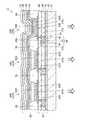
続いて、第1の実施形態に係る有機EL装置の構造について図3を参照して説明する。図3は、第1の実施形態に係る有機EL装置の構造を示す模式断面図である。なお、本明細書では、図3における有機EL装置11の陰極25側を上方と呼ぶ。また、本明細書では、有機EL装置11の陰極25側表面の法線方向から見ることを「平面視」と呼ぶ。 Next, the structure of the organic EL device according to the first embodiment will be described with reference to FIG. FIG. 3 is a schematic cross-sectional view showing the structure of the organic EL device according to the first embodiment. In the present specification, the
図3に示すように、有機EL装置11は、基板31と、基板31上に形成された回路素子層43と陽極24(24R,24G,24B)と隔壁(バンク)58と発光機能層26と陰極(共通電極)25と、を備えている。陽極24は、サブ画素34Rに設けられた第1陽極としての陽極24Rと、サブ画素34Bに設けられた第2陽極としての陽極24Bと、サブ画素34Gに設けられた第3陽極としての陽極24Gと、を有する。以下では、対応する色を区別しない場合には、単に陽極24と記す。 As shown in FIG. 3, the
有機EL装置11は、発光機能層26から発した光が発光領域32(図2参照)において基板31側に射出されるボトムエミッション型である。基板31は、有機EL装置11がボトムエミッション型であることから、基材に透光性材料が用いられる。透光性材料としては、例えば、ガラス、石英、樹脂(プラスチック、プラスチックフィルム)等があげられる。 The
回路素子層43は、下地保護膜45と、駆動用トランジスター23と、第1層間絶縁膜54と、第2層間絶縁膜55とを備えている。下地保護膜45は、例えば、シリコン酸化膜(SiO2)からなり、基板31を覆って形成されている。The
駆動用トランジスター23は、下地保護膜45上に、サブ画素34(34R,34G,34B)毎に形成されている。駆動用トランジスター23は、半導体膜46とゲート絶縁膜52とゲート電極23gとドレイン電極23dとソース電極23sとを有している。半導体膜46は、ポリシリコン膜からなり、下地保護膜45上に島状に形成されている。半導体膜46には、ソース領域47及びドレイン領域48が不純物の導入によって形成されている。そして、不純物が導入されなかった部分がチャネル領域51となっている。 The driving
ゲート絶縁膜52は、シリコン酸化膜等の透明な絶縁膜からなり、下地保護膜45と半導体膜46とを覆って形成されている。ゲート絶縁膜52上には、ゲート電極23gが形成されている。ゲート電極23gは、アルミニウム(Al)、モリブデン(Mo)、タンタル(Ta)、チタン(Ti)、タングステン(W)等からなり、平面視で半導体膜46のチャネル領域51に重なる位置に設けられている。 The
第1層間絶縁膜54は、例えば、シリコン酸化膜(SiO2)、チタン酸化膜(TiO2)等からなり、ゲート絶縁膜52とゲート電極23gとを覆って形成されている。第1層間絶縁膜54上には、ソース電極23sとドレイン電極23dとが形成されている。The first
ソース電極23sは、第1層間絶縁膜54に設けられたコンタクトホールを介して、半導体膜46のソース領域47に電気的に接続されている。ドレイン電極23dは、第1層間絶縁膜54に設けられたコンタクトホールを介して、半導体膜46のドレイン領域48に導電接続されている。 The source electrode 23 s is electrically connected to the
第2層間絶縁膜55は、例えば、シリコン酸化膜(SiO2)、チタン酸化膜(TiO2)等からなり、第1層間絶縁膜54とソース電極23sとドレイン電極23dとを覆って形成されている。第2層間絶縁膜55は、アクリル樹脂等で構成されていてもよい。The second
陽極24(24R,24G,24B)は、第2層間絶縁膜55上に、サブ画素34(34R,34G,34B)毎に形成されている。陽極24は、例えば、平面視で略矩形状の形状となっている。陽極24の膜厚は、特に限定されないが、例えば10nm〜200nm程度であり、好ましくは30nm〜150nm程度である。陽極24は、第2層間絶縁膜55に設けられたコンタクトホールを介して、駆動用トランジスター23のドレイン電極23dに電気的に接続されている。 The anode 24 (24R, 24G, 24B) is formed on the second
第2層間絶縁膜55上には、隔壁58が、平面視で略格子状に設けられている。隔壁58は、例えば、断面が傾斜面を有する台形状であり、隣り合う陽極24間の絶縁性を確保するとともに、サブ画素34の形状を所望の形状(例えば、トラック形状)にするために、陽極24の周縁部に所定幅で乗り上げるように形成されている。換言すれば、隔壁58の開口部が、サブ画素34の領域となる。 On the second
隔壁58は、例えば、アクリル樹脂、ポリイミド樹脂等の耐熱性、耐溶剤性を有する有機材料からなる。なお、後述するように、発光機能層26のうちの一部の層をインクジェット法等の塗布方式を用いて形成する場合は、隔壁58の表面が撥液性を有していることが望ましい。なお、第2層間絶縁膜55と隔壁58との間に、例えば、シリコン酸化膜(SiO2)等の無機材料からなる絶縁層が設けられていてもよい。The
発光機能層26は、サブ画素34(34R,34G,34B)毎、すなわち、発光素子27(27R,27G,27B)毎に異なる構成を有している。サブ画素34R(赤色発光素子27R)においては、隔壁58によって囲まれた領域の陽極24R上に、第1正孔注入層としての正孔注入層61Rと、正孔輸送層62Rと、第1発光層(赤色発光層)としての発光層63Rとが、塗布方式によって順に形成されている。 The light emitting
サブ画素34G(緑色発光素子27G)においては、隔壁58によって囲まれた領域の陽極24G上に、第3正孔注入層としての正孔注入層61Gと、正孔輸送層62Gと、第4発光層(緑色発光層)としての発光層63Gとが、塗布方式によって順に形成されている。 In the sub-pixel 34G (green
サブ画素34B(青色発光素子27B)においては、隔壁58によって囲まれた領域の陽極24B上に、第2正孔注入層としての正孔注入層61Bと、正孔輸送層62Bとが、塗布方式によって順に形成されている。 In the sub-pixel 34B (blue
正孔注入層61R,61G,61Bは、陽極24R,24G,24Bからの正孔の注入効率を向上する機能を有する。正孔注入層61R,61G,61Bの膜厚は、特に限定されないが、例えば5nm〜100nm程度であり、好ましくは5nm〜50nm程度であり、より好ましくは10nm〜40nm程度である。以下では、対応する色を区別しない場合には、単に正孔注入層61と記す。 The hole injection layers 61R, 61G, and 61B have a function of improving hole injection efficiency from the
正孔輸送層62R,62G,62Bは、注入された正孔の発光層63R,63G,63Bへの輸送を促進する機能を有する。正孔輸送層62R,62G,62Bの膜厚は、特に限定されないが、例えば5nm〜100nm程度であり、好ましくは10nm〜50nm程度である。以下では、対応する色を区別しない場合には、単に正孔輸送層62と記す。なお、サブ画素34R,34G,34Bにおいて、正孔輸送層62R,62G,62Bを省略した構成としてもよい。 The
また、発光層63R,63Gの膜厚は、特に限定されないが、例えば10nm〜150nm程度であり、好ましくは20nm〜100nm程度であり、より好ましくは50nm〜80nm程度である。 The thickness of the
発光層63R,63G、正孔輸送層62B、及び隔壁58上には、サブ画素34R,34G,34Bに亘って、可視光波長域以外の波長の光である赤外光を発光する機能を有する第3発光層としての赤外発光層64が形成されている。赤外発光層64は、蒸着方式を用いて形成されていることが好ましい。塗布方式で形成された発光層63R,63G上に塗布方式で赤外発光層64を形成する場合、赤外発光層64を形成する工程において発光層63R,63Gに溶融や変質等が生じて発色品質に影響を及ぼすおそれがあるが、このような発光層63R,63Gの発色品質への影響を抑えることができる。また、蒸着方式で形成されていると、塗布方式で形成される場合に比べて、赤外発光層64をより緻密な膜とすることができる。 On the
赤外発光層64の膜厚は、特に限定されないが、例えば1nm〜50nm程度であり、好ましくは5nm〜20nm程度である。なお、赤外発光層64の膜厚が厚くなり過ぎると、サブ画素34Bにおいて、陽極24側から発光層63Bへ輸送される正孔のうち、赤外発光層64で消費される正孔が多くなってしまい、発光層63Bでの発光効率の低下を招くこととなる。 The film thickness of the infrared
赤外発光層64上には、サブ画素34R,34G,34Bに亘って、青色を発光する機能を有する第2発光層(青色発光層)としての発光層63Bが蒸着方式により形成されている。赤外発光層64と発光層63Bとは、サブ画素34R,34G,34Bに亘って形成されるため、精密アライメントマスク等を用いたパターニングを必要としないので、有機EL装置11の生産性向上及びコスト低減を図ることができる。発光層63Bの膜厚は、特に限定されないが、例えば5nm〜100nm程度であり、好ましくは10nm〜50nm程度である。 On the infrared
発光層63B上には、電子輸送層65が蒸着方式により形成されている。電子輸送層65は、陰極25から注入された電子の発光層63R,63G,63Bへの輸送を促進する機能を有する。電子輸送層65の膜厚は、特に限定されないが、例えば1nm〜100nm程度であり、好ましくは5nm〜50nm程度である。なお、電子輸送層65を省略した構成としてもよい。 An
電子輸送層65上には、電子注入層66が蒸着方式により形成されている。電子注入層66は、陰極25からの電子の注入効率を向上する機能を有する。電子注入層66の膜厚は、特に限定されないが、例えば0.01nm〜100nm程度であり、好ましくは0.1nm〜10nm程度である。 An
これらの正孔注入層61R,61G,61Bと、正孔輸送層62R,62G,62Bと、発光層63R,63G,63Bと、赤外発光層64と、電子輸送層65と、電子注入層66とにより、発光機能層26が構成される。発光機能層26において、サブ画素34Bにおける陽極24Bと発光層63Bとの間の距離は、サブ画素34R,34Gにおける陽極24R,24Gと発光層63Bとの間の距離よりも小さい。 These hole injection layers 61R, 61G, 61B,
換言すれば、サブ画素34Bにおける正孔注入層61Bの膜厚と正孔輸送層62Bの膜厚と赤外発光層64の膜厚との総和は、サブ画素34R,34Gにおける正孔注入層61R,61Gの膜厚と正孔輸送層62R,62Gの膜厚と発光層63R,63Gの膜厚と赤外発光層64の膜厚との総和よりも小さい。これにより、サブ画素34Bにおいては、サブ画素34R,34Gと比べて、発光層63Bまで到達する正孔が多くなるので、発光層63Bでの青色の発光効率が向上する。 In other words, the sum of the thickness of the
発光機能層26(電子輸送層65)上には、陰極25が、基板31上の全面に形成されている。陰極25の膜厚は、特に限定されないが、例えば50nm〜1000nm程度であり、好ましくは100nm〜500nm程度である。 A
陰極25上には、封止基板(図示しない)が設けられている。封止基板は、発光素子27(27R,27G,27B)を、酸素や水分あるいは外力から保護するためのものである。封止基板は、例えば、エポキシ等の接着剤を介して陰極25と接合される。封止基板は、平坦な基板に限定されず、凹型のガラスや金属等で構成されていてもよい。 On the
上述のように、有機EL装置11は、インクジェット法等の塗布方式(液相プロセス)によって形成された発光層63R,63Gと、蒸着方式(気相プロセス)よって形成された発光層63Bとを有しており、3原色でのフルカラー表示が可能である。 As described above, the
塗布方式は、パターニング性が高いこと、大面積化が容易であること、材料の使用効率が高いこと、等の利点があり、生産性に優れる。しかしながら、塗布方式を用いて形成された発光層では、赤色発光層及び緑色発光層は発光効率や発光寿命(連続駆動の耐久性)等の特性において実用レベルにあるものの、青色発光層は実用レベルに到達したとは言い難い。一方、蒸着方式を用いて形成された青色発光層は、発光効率や発光寿命等の特性において実用レベルに到達しており、塗布方式を用いて形成された赤色発光層及び緑色発光層よりも優れる場合がある。 The coating method has advantages such as high patterning property, easy area enlargement, and high material use efficiency, and is excellent in productivity. However, in the light emitting layer formed by using the coating method, the red light emitting layer and the green light emitting layer are at a practical level in characteristics such as light emission efficiency and light emission lifetime (durability of continuous driving), but the blue light emitting layer is at a practical level. It ’s hard to say that On the other hand, the blue light emitting layer formed using the vapor deposition method has reached a practical level in characteristics such as light emission efficiency and light emission lifetime, and is superior to the red light emitting layer and the green light emitting layer formed using the coating method. There is a case.
ところで、特許文献1及び特許文献2に記載の有機EL装置の構成によれば、塗布方式によって形成された赤色発光層及び緑色発光層上に、青色発光層が蒸着方式により形成されている。そのため、陽極から赤色発光層及び緑色発光層に注入された正孔のうち、赤色発光層及び緑色発光層を通過した正孔が青色発光層に到達して電子と再結合すると、青色発光層で青色発光が生じてしまう。そうすると、赤色発光層からの赤色発光及び緑色発光層からの緑色発光に青色発光層からの青色発光の混色が生じて色純度が低下し、有機EL装置の発色品質が低下するおそれがあるという課題があった。 By the way, according to the structure of the organic EL device described in Patent Document 1 and Patent Document 2, the blue light emitting layer is formed by the vapor deposition method on the red light emitting layer and the green light emitting layer formed by the coating method. Therefore, among the holes injected from the anode into the red light emitting layer and the green light emitting layer, when the holes that have passed through the red light emitting layer and the green light emitting layer reach the blue light emitting layer and recombine with electrons, Blue light emission occurs. Then, the red light emission from the red light emission layer and the green light emission from the green light emission layer are mixed with blue light emission from the blue light emission layer, the color purity is lowered, and the color development quality of the organic EL device may be lowered. was there.
これに対して、有機EL装置11では、蒸着方式により形成された発光層63Bが、3つのサブ画素34R,34G,34Bに亘って設けられており、サブ画素34R,34Gにおいて発光層63R,63Gの上層に位置している点では、特許文献1及び特許文献2に記載の有機EL装置と同様である。 On the other hand, in the
しかしながら、有機EL装置11では、発光層63R,63Gと発光層63Bとの間に赤外発光層64が設けられているので、発光層63R,63Gを通過して発光層63Bに向かう正孔は、発光層63R,63Gと発光層63Bとの間に介在する赤外発光層64で電子と再結合して消費される。そのため、赤外発光層64が設けられていない場合に比べて、サブ画素34R,34Gにおいて、発光層63Bまで到達する正孔が少なくなるので、発光層63Bの青色の発光が抑えられる。 However, in the
また、サブ画素34R,34G,34Bにおいて、赤外発光層64で正孔と電子とが再結合しても赤外光が発光されるので、赤色、緑色、及び青色の発光との混色は生じない。これにより、サブ画素34R,34G,34Bにおける赤色、緑色、及び青色の発光のそれぞれの色純度を高めることができるので、高い発色品質を有する有機EL装置11を提供することができる。 In addition, in the sub-pixels 34R, 34G, and 34B, infrared light is emitted even when holes and electrons are recombined in the infrared
<各層の構成材料>
続いて、有機EL装置11の各層の構成材料を説明する。陽極24の構成材料としては、特に限定されないが、仕事関数が大きく、導電性に優れる材料が好適に用いられる。陽極24の構成材料としては、例えば、ITO(Indium Tin Oxide)、IZO(Indium Zinc Oxide)、In2O3、SnO2、フッ素添加SnO2、Sb添加SnO2、ZnO、Al添加ZnO、Ga添加ZnO等の金属酸化物、Au、Pt、Ag、Cu、またはこれらを含む合金等が挙げられ、これらのうちの1種または2種以上を組み合わせて用いることができる。陽極24には光透過性が求められるため、上述した構成材料のうち、光透過性を有する金属酸化物が好適に用いられる。<Constituent materials for each layer>
Then, the constituent material of each layer of the
正孔注入層61の構成材料としては、特に限定されないが、塗布方式を用いて正孔注入層61を形成し得るように、導電性高分子材料(または導電性オリゴマー材料)に電子受容性ドーパントを添加したイオン伝導性正孔注入材料が好適に用いられる。 The constituent material of the hole injection layer 61 is not particularly limited, but an electron-accepting dopant is added to the conductive polymer material (or conductive oligomer material) so that the hole injection layer 61 can be formed using a coating method. An ion conductive hole injection material to which is added is suitably used.
このようなイオン伝導性正孔注入材料としては、例えば、PEDOT/PSS(Poly(3,4-ethylenedioxythiophene)-poly(styrenesulfonate))のようなポリチオフォン系正孔注入材料や、PANI/PSS(Polyaniline-poly(styrenesulfonate))のようなポリアニリン系正孔注入材料が挙げられる。 Examples of such ion conductive hole injection materials include polythiophonic hole injection materials such as PEDOT / PSS (Poly (3,4-ethylenedioxythiophene) -poly (styrenesulfonate)), PANI / PSS (Polyaniline- and polyaniline hole injection material such as poly (styrenesulfonate).
正孔輸送層62の構成材料としては、特に限定されないが、塗布方式を用いて正孔輸送層62を形成し得るように、例えば、下記化1に示すTFB(poly(2,7-(9,9-di-n-octylfluorene)-alt-(1,4-phenylene-((4-sec-butylphenyl)imino-1,4-phenylene))))等のトリフェニルアミン系ポリマーを含んだ材料を用いることができる。 The constituent material of the hole transport layer 62 is not particularly limited. For example, a TFB (poly (2,7- (9) shown in the following chemical formula 1 can be used to form the hole transport layer 62 using a coating method. , 9-di-n-octylfluorene) -alt- (1,4-phenylene-((4-sec-butylphenyl) imino-1,4-phenylene)))) and other materials containing triphenylamine polymers Can be used.

発光層63R,63Gの構成材料は、特に限定されないが、塗布方式を用いて発光層63R,63Gを形成し得るように、溶液化または分散液化できることが望ましい。そこで、溶媒または分散媒に溶解または分散することができる、高分子材料及び低分子発光材料が好適に用いられる。 The constituent materials of the
赤色の発光層63Rの構成材料としては、例えば、下記化2に示すアメリカンダイソース社(American Dye Source,Inc.)製のADS−111RE(Poly[{9,9-dihexyl-2,7-bis(1-cyanovinylene)fluorenylene}-alt-co-{2,5-bis(N,N−diphenylamino)-1,4-phenylene}])を用いることができる。 As a constituent material of the red
緑色の発光層63Gの構成材料としては、例えば、下記化3に示すアメリカンダイソース社(American Dye Source,Inc.)製のADS−109GE(Poly[(9,9-dioctyl-2,7-bis{2-cyanovinylenefluorenylene})-alt-co-(2-methoxy-5-{2-ethylhexyloxy}-1,4-phenylene)])を用いることができる。 As a constituent material of the green
赤外発光層64の構成材料は、赤外発光材料をゲスト材料としてホスト材料にドープしたものを用いることができる。赤外発光するゲスト材料としては、ポルフィリン錯体やフタロシアニン錯体を好適に用いることができる。ポルフィリン錯体として、例えば、下記化4に示す2,3,7,8,12,13,17,18-Octaethyl-21H,23H-porphine iron(III) chloride、下記化5に示す2,3,7,8,12,13,17,18-Octaethyl-21H,23H-porphine nickel(II)を用いることができる。また、下記化6に示す5,10,15,20-Tetraphenyl-21H,23H-porphine nickel(II)、下記化7に示すPlatinum(II)2,3,7,8,12,13,17,18-octaethyl-21H,23H-porphyrin等も用いることができる。 As a constituent material of the infrared
赤外発光層64のホスト材料としては、特に限定されないが、例えば、下記化8に示すAlq3(tris(8-hydroxyquinolinato)aluminium)のような金属錯体や、下記化9に示す4,4'-Bis(N-carbazolyl)-1,1'-biphenylのようなカルバゾール誘導体等を用いることができる。赤外発光層64におけるゲスト材料の含有量(ドープ量)は、ホスト材料に対して重量比で0.1%〜20%程度であることが好ましい。 The host material of the infrared
青色の発光層63Bの構成材料としては、特に限定されないが、例えば、蒸着方式を用いて発光層63Bを形成し得るように、例えば、下記化10に示すスチリル誘導体の青色発光材料である4,4'-Bis(2,2-diphenyl-ethen-1-yl)biphenylが挙げられる。 The constituent material of the blue light-emitting
また、青色の発光層63Bの構成材料としては、青色発光材料をゲスト材料としてホスト材料にドープしたものを用いることができる。ホスト材料は、正孔と電子との再結合により励起子を生成するとともに、その励起子のエネルギーを青色発光材料に移動(フェルスター移動またはデクスター移動)させて青色発光材料を励起する機能を有する。このホスト材料の機能により、ゲスト材料である青色発光材料が効率よく励起され、発光する。 In addition, as a constituent material of the blue
このようなホスト材料としては、例えば、アントラセン誘導体の下記化11に示す9,10-Di(naphth-2-yl)anthracene、下記化12に示す9-(4-(naphth-1-yl)-phenyl)-10-(naphth-2-yl)anthracene、及び下記化13に示す9,9’-di(biphenyl-2-yl)-bianthraceneが挙げられ、これらのうちの1種または2種以上を組み合わせて用いることができる。 Examples of such host materials include 9,10-Di (naphth-2-yl) anthracene represented by the following
また、ゲスト材料(青色発光材料)としては、例えば、下記化14、下記化15、及び下記化16に示すスチリル誘導体が挙げられ、これらのうちの1種または2種以上を組み合わせて用いることができる。 Examples of the guest material (blue light-emitting material) include styryl derivatives shown in the following
発光層63Bにおけるゲスト材料の含有量(ドープ量)は、例えば、ホスト材料に対して重量比で0.1%〜20%程度であり、0.5%〜10%程度であることがより好ましい。ゲスト材料の含有量をこのような範囲内とすることで、発光層63Bにおける発光効率を最適化することができる。 The content (dope amount) of the guest material in the
電子輸送層65の構成材料としては、特に限定されないが、例えば、Alq3(上記化8参照)やLiq(8-Hydroxyquinolinolato-lithium)等の8−キノリノールまたはその誘導体を配位子とする有機金属錯体等のキノリン誘導体を好適に用いることができる。また、tBu−PBD(2-(4'-tert-Butylphenyl)-5-(4"-biphenyl)-1,3,4-oxadiazole)やBND(2,5,-Bis(1-naphthyl)-1,3,4-oxadiazole)等のオキサジアゾール誘導体、シロール誘導体、ピリジン誘導体、ピリミジン誘導体、キノキサリン誘導体、イミダゾール誘導体等も好適に用いることができる。そして、これらのうちの1種または2種以上を組み合わせて用いることができる。 The constituent material of the
電子注入層66の構成材料は、電子注入材料と金属材料とを含んでいる。電子注入材料としては、例えば、アルカリ金属、アルカリ土類金属、希土類金属、アルカリ金属塩(酸化物、フッ化物、塩化物等)、アルカリ土類金属塩(酸化物、フッ化物、塩化物等)、希土類金属塩(酸化物、フッ化物、塩化物等)、金属錯体等のような電子注入材料が挙げられ、これらのうちの1種または2種以上と金属材料とを組み合わせて用いることができる。 The constituent material of the
アルカリ金属としては、例えば、Li、Na、K、Rb、Csが挙げられる。アルカリ土類金属としては、例えば、Mg、Ca、Sr、Baが挙げられる。希土類金属としては、例えば、Nd、Sm、Y、Tb、Euが挙げられる。アルカリ金属塩としては、例えば、LiF、Li2CO3、LiCl、NaF、Na2CO3、NaCl、CsF、Cs2CO3、CsClが挙げられる。Examples of the alkali metal include Li, Na, K, Rb, and Cs. Examples of the alkaline earth metal include Mg, Ca, Sr, and Ba. Examples of rare earth metals include Nd, Sm, Y, Tb, and Eu. Examples of the alkali metal salt include LiF, Li2 CO3 , LiCl, NaF, Na2 CO3 , NaCl, CsF, Cs2 CO3 , and CsCl.
アルカリ土類金属塩としては、例えば、CaF2、CaCO3、SrF2、SrCO3、BaF2、BaCO3が挙げられる。希土類金属塩としては、例えば、SmF3、ErF3が挙げられる。金属錯体としては、例えば、Alq3やLiq等の8−キノリノールなしいその誘導体を配位子とする有機金属錯体が挙げられる。また、金属材料としては、例えば、Ag、Al、Cu、Auが挙げられる。Examples of the alkaline earth metal salt include CaF2 , CaCO3 , SrF2 , SrCO3 , BaF2 , and BaCO3 . Examples of the rare earth metal salt include SmF3 and ErF3 . Examples of the metal complex include organometallic complexes having 8-quinolinol or a derivative thereof such as Alq3 or Liq as a ligand. Examples of the metal material include Ag, Al, Cu, and Au.
陰極25の構成材料としては、仕事関数の小さい材料を用いることが好ましい。陰極25の構成材料としては、蒸着方式を用いて形成し得るように、例えば、Li、Mg、Ca、Sr、La、Ce、Er、Eu、Sc、Y、Yb、Ag、Cu、Al、Cs、Rb、Au、またはこれらを含む合金等が用いられ、これらのうちの1種または2種以上を組み合わせて(例えば、複数層の積層体等として)用いることができる。 As a constituent material of the
<有機EL装置の製造方法>
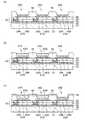
次に、第1の実施形態に係る有機EL装置の製造方法を図を参照して説明する。図4〜図6は、第1の実施形態に係る有機EL装置の製造方法を説明する模式断面図である。なお、公知の方法を採用することができる工程については、詳細な説明を省略する。<Method for manufacturing organic EL device>
Next, a method for manufacturing the organic EL device according to the first embodiment will be described with reference to the drawings. 4 to 6 are schematic cross-sectional views illustrating the method for manufacturing the organic EL device according to the first embodiment. In addition, detailed description is abbreviate | omitted about the process which can employ | adopt a well-known method.
まず、図4(a)に示すように、基板31上に、公知の成膜技術やフォトリソ技術を用いて回路素子層43(詳細は、図3参照)を形成する。そして、回路素子層43上に、サブ画素34(34R,34G,34B)毎に、ITO等からなる陽極24(24R,24G,24B)を形成する。 First, as shown in FIG. 4A, a circuit element layer 43 (refer to FIG. 3 for details) is formed on a
次に、図4(b)に示すように、回路素子層43及び陽極24上に、隔壁58を形成する。詳しくは、まず、隔壁58の材料であるアクリル樹脂を含む溶液を回路素子層43(第2層間絶縁膜55)上及び陽極24上に塗布する。そして、塗布した溶液を乾燥させて隔壁層を形成する。その後、この隔壁層におけるサブ画素34(34R,34G,34B)に対応する領域に開口部を形成する。これにより、隔壁58が完成する。 Next, as shown in FIG. 4B, a
ここで、発光機能層26のうちの一部の層はインクジェット法等の塗布方式を用いて形成されるので、隔壁58の表面が撥液性を有していることが望ましい。隔壁58に撥液性を持たせる方式としては、例えば、フッ素等の撥液成分を予め混入させた樹脂(例えばアクリル樹脂)を用い、隔壁形成工程におけるキュア時において撥液成分を樹脂表層に拡散集積させる方法がある。 Here, since a part of the light emitting
なお、回路素子層43と隔壁58との間に絶縁層を形成する場合は、例えば、シリコン酸化膜(SiO2)からなる絶縁膜を、CVD(Chemical Vapor Deposition)法等により、回路素子層43及び陽極24上を覆うように成膜形成する。そして、フォトリソグラフィー技術及びエッチング技術を用いて、絶縁膜のうちサブ画素34(34R,34G,34B)に対応する領域に開口部を形成する。When an insulating layer is formed between the
次に、図4(c)に示すように、サブ画素34(34R,34G,34B)の各領域において、隔壁58によって囲まれた陽極24(24R,24G,24B)上に、正孔注入層61(61R,61G,61B)を、塗布方式により、例えば5nm〜100nm程度の膜厚で形成する。 Next, as shown in FIG. 4C, the hole injection layer is formed on the anode 24 (24R, 24G, 24B) surrounded by the
詳しくは、正孔注入層61の材料を含んだ機能液を液滴吐出法(例えば、インクジェット法)により吐出する。正孔注入層61の機能液としては、例えば、PEDOT/PSSやPANI/PSS等を溶媒または分散媒に溶解または分散させたものを用いることができる。陽極24上に機能液を塗布した後、機能液を乾燥させ大気下で焼成して溶媒または分散媒を除去することにより、正孔注入層61が形成される。 Specifically, the functional liquid containing the material for the hole injection layer 61 is discharged by a droplet discharge method (for example, an ink jet method). As the functional liquid of the hole injection layer 61, for example, a solution obtained by dissolving or dispersing PEDOT / PSS, PANI / PSS, or the like in a solvent or a dispersion medium can be used. After the functional liquid is applied on the
続いて、図5(a)に示すように、サブ画素34(34R,34G,34B)の各領域において、正孔注入層61(61R,61G,61B)上に、正孔輸送層62(62R,62G,62B)をそれぞれ、塗布方式により、例えば5nm〜100nmの膜厚で形成する。 Subsequently, as shown in FIG. 5A, in each region of the sub-pixel 34 (34R, 34G, 34B), the hole transport layer 62 (62R) is formed on the hole injection layer 61 (61R, 61G, 61B). , 62G, 62B) are formed with a film thickness of, for example, 5 nm to 100 nm by a coating method.
詳しくは、正孔輸送層62の材料を含んだ機能液を液滴吐出法(例えば、インクジェット法)により吐出する。正孔輸送層62の機能液としては、例えば、TFBをシクロヘキシルベンゼンに溶解させたインク組成物を用いることができる。塗布した後、機能液を乾燥させ低酸素環境下で焼成することにより、正孔輸送層62が形成される。 Specifically, the functional liquid containing the material for the hole transport layer 62 is discharged by a droplet discharge method (for example, an ink jet method). As the functional liquid for the hole transport layer 62, for example, an ink composition in which TFB is dissolved in cyclohexylbenzene can be used. After the application, the hole transport layer 62 is formed by drying the functional liquid and baking it in a low oxygen environment.
次に、図5(b)に示すように、サブ画素34Rにおける正孔輸送層62R上に、発光層63Rを、塗布方式により、例えば10nm〜150nm程度の膜厚で形成する。また、サブ画素34Gにおける正孔輸送層62G上に、発光層63Gを、塗布方式により、例えば10nm〜150nm程度の膜厚で形成する。 Next, as illustrated in FIG. 5B, the
詳しくは、赤色または緑色の発光材料を含んだ機能液を液滴吐出法(例えば、インクジェット法)により吐出し、その後機能液を乾燥させ、不活性雰囲気下で焼成する。発光材料の機能液としては、例えば、上記化2または上記化3で示された発光材料が溶媒に溶解されたものを用いることができる。溶媒としては、シクロヘキシルベンゼンなどが挙げられる。 Specifically, a functional liquid containing a red or green light emitting material is discharged by a droplet discharge method (for example, an ink jet method), and then the functional liquid is dried and baked in an inert atmosphere. As the functional liquid of the luminescent material, for example, a solution obtained by dissolving the luminescent material represented by Chemical Formula 2 or
次に、図5(c)に示すように、サブ画素34R,34G,34Bに亘って、サブ画素34Rにおける発光層63R上と、サブ画素34Gにおける発光層63G上と、サブ画素34Bにおける正孔輸送層62B上と、隔壁58上とに、赤外発光層64を、蒸着方式により形成する。赤外発光層64は、例えば、金属錯体やカルバゾール誘導体等のホスト材料と、ホスト材料に対して重量比で0.1%〜20%程度のポルフィリン錯体等のゲスト材料とを用いて、1nm〜50nm程度の膜厚で形成する。 Next, as shown in FIG. 5C, over the sub-pixels 34R, 34G, and 34B, holes on the light-emitting
次に、図6(a)に示すように、サブ画素34R,34G,34Bに亘って、赤外発光層64上に発光層63Bを、蒸着方式により形成する。発光層63Bは、例えば、アントラセン誘導体等のホスト材料と、ホスト材料に対して重量比で0.1%〜20%程度のスチリル誘導体等のゲスト材料とを用いて、5nm〜100nm程度の膜厚で形成する。 Next, as shown in FIG. 6A, a
次に、図6(b)に示すように、サブ画素34R,34G,34Bに亘って、発光層63B上に電子輸送層65を、蒸着方式により形成する。電子輸送層65は、例えば、キノリン誘導体やオキサジアゾール誘導体等を用いて、1nm〜100nm程度の膜厚で形成する。 Next, as shown in FIG. 6B, an
次に、図6(c)に示すように、サブ画素34R,34G,34Bに亘って、電子輸送層65上に電子注入層66を、蒸着方式により形成する。電子注入層66は、例えば、電子注入材料と金属材料とを用いて、0.01nm〜100nm程度の膜厚で形成する。これにより、発光機能層26が完成する。 Next, as shown in FIG. 6C, an
次に、図3に示すように、電子輸送層65上に陰極25を蒸着方式により形成する。陰極25は、例えば、仕事関数の小さい金属材料を用いて、50nm〜1000nm程度の膜厚で形成する。その後、図示しないが、陰極25上にエポキシ等の接着剤を介して封止基板を接合する。以上により、有機EL装置11が完成する。 Next, as shown in FIG. 3, the
以上説明したように、第1の実施形態によれば、以下に示す効果が得られる。 As described above, according to the first embodiment, the following effects can be obtained.
(1)発光層63R,63Gと発光層63Bとの間に赤外発光層64が設けられているので、陽極24から発光層63R,63Gに注入された正孔のうち発光層63R,63Gを通過して発光層63Bに向かう正孔は、赤外発光層64で電子と再結合して消費される。そのため、赤外発光層64が設けられていない場合に比べて、発光層63Bまで到達する正孔が少なくなるので、サブ画素34R,34Gにおける青色の発光が抑えられる。これにより、赤色及び緑色の発光の色純度を高めることができる。 (1) Since the infrared
(2)赤外発光層64が可視光波長域以外の赤外光を発光するので、赤外発光層64で正孔と電子とが再結合しても、サブ画素34R,34G,34Bにおける赤色、緑色、及び青色の発光との混色は生じない。これにより、サブ画素34R,34G,34Bにおける赤色、緑色、及び青色の発光の色純度を高めることができるので、高い発色品質を有する有機EL装置11を提供することができる。 (2) Since the infrared
(3)赤外発光層64は、その構成材料にポルフィリン錯体を含んでいるので、サブ画素34R,34G,34Bにおける赤色、緑色、及び青色の発光との混色が生じない可視光波長域以外の赤外光を発光することにより、発光層63R,63Gを通過した正孔を消費することができる。 (3) Since the infrared
(4)赤外発光層64が蒸着方式で形成されているので、塗布方式で形成される場合に比べて、赤外発光層64をより緻密な膜とすることができる。また、サブ画素34R,34G,34Bに亘って形成されるため、精密アライメントマスク等を用いたパターニングを必要としないので、有機EL装置11の生産性向上及びコスト低減を図ることができる。 (4) Since the infrared
(5)正孔注入層61R,61G,61Bが設けられているので、陽極24R,24Gから発光層63R,63Gへの正孔注入と陽極24Bから発光層63Bへの正孔注入とが効率良く行われる。ここで、サブ画素34Bにおいては陽極24Bと発光層63Bとの間に発光層63R,63Gが設けられておらず、かつ、サブ画素34Bにおける陽極24Bと発光層63Bとの間の距離は、サブ画素34R,34Gにおける陽極24R,24Gと発光層63R,63Gとの間の距離よりも小さい。そのため、サブ画素34Bにおいては、サブ画素34R,34Gと比べて、発光層63Bまで到達する正孔が多くなるので、発光層63Bでの青色の発光効率が向上する。これらの結果により、高い発色品質を有する有機EL装置11を提供することができる。 (5) Since the hole injection layers 61R, 61G, 61B are provided, the hole injection from the
(6)生産性に優れる塗布方式で実用的な発光特性が得られている赤色発光材料及び緑色発光材料を発光層63R,63Gに用いるとともに、塗布方式では実用的な性能が得られていないものの、蒸着方式では実用的な性能に達している青色発光材料を発光層63Bに用いることができる。これにより、フルカラー表示が可能で発色品質、発光効率、及び発光寿命に優れる有機EL装置11を提供することができる。 (6) Although a red light emitting material and a green light emitting material, which have practical light emitting characteristics obtained by a coating method with excellent productivity, are used for the
(第2の実施形態)
<電子機器>
次に、第2の実施形態に係る電子機器の構成を説明する。図7は、第2の実施形態に係る電子機器の一例として、テレビの構成を模式的に示す概略斜視図である。以下、第2の実施形態に係るテレビの構成を、図7を参照して説明する。(Second Embodiment)
<Electronic equipment>
Next, the configuration of the electronic device according to the second embodiment will be described. FIG. 7 is a schematic perspective view schematically showing a configuration of a television as an example of the electronic apparatus according to the second embodiment. The configuration of the television according to the second embodiment will be described below with reference to FIG.
図7に示すように、第2の実施形態に係るテレビ101は、表示部102と、枠部103と、脚部104と、リモコン(リモートコントローラー)105とを有する。表示部102には、第1の実施形態に係る有機EL装置11が実装されている。枠部103は、表示部102をガイドするために用いられる。脚部104は、表示部102及び枠部103を一定の高さで固定するために用いられる。リモコン105は、例えば、テレビ101の電源をON/OFFしたり、チャンネルを変えたりするために用いられる。 As illustrated in FIG. 7, the
第2の実施形態に係るテレビ101は、表示部102に、第1の実施形態に係る有機EL装置11を備えているので、高い発色品質、発光効率、及び発光寿命を有している。 Since the
なお、電子機器は、テレビの他に、例えば、ディスプレイ、携帯電話機、モバイルコンピューター、デジタルカメラ、デジタルビデオカメラ、カーナビゲーション装置、オーディオ機器等であってもよい。これらの電子機器であっても、第1の実施形態に係る有機EL装置11を備えることで、発光寿命及び発光効率に優れ、高い発色品質を有する電子機器を提供することができる。 In addition to the television, the electronic device may be a display, a mobile phone, a mobile computer, a digital camera, a digital video camera, a car navigation device, an audio device, or the like. Even with these electronic devices, by providing the
上述した実施形態は、あくまでも本発明の一態様を示すものであり、本発明の範囲内で任意に変形及び応用が可能である。変形例としては、例えば、以下のようなものが考えられる。 The above-described embodiments merely show one aspect of the present invention, and can be arbitrarily modified and applied within the scope of the present invention. As modifications, for example, the following can be considered.
(変形例1)
第1の実施形態に係る有機EL装置11では、赤外発光層64が、サブ画素34R,34G,34Bに亘って形成された構成を備えていたが、本発明はこのような形態に限定されない。例えば、赤外発光層64を塗布方式で形成すること等により、赤外発光層64がサブ画素34R,34Gにおいて発光層63R,63G上に選択的に設けられた構成としてもよい。このような構成にすれば、赤外発光層64が設けられないサブ画素34Bにおいて、陽極24Bから発光層63Bに到達する正孔をより多くできるので、青色の発光効率を向上させることができる。(Modification 1)
In the
(変形例2)
第1の実施形態に係る有機EL装置11では、第3発光層(赤外発光層64)が赤外光を発光する構成を備えていたが、本発明はこのような形態に限定されない。第3発光層が発光する光は、可視光波長域以外の波長の光であれば、赤外光以外の光、例えば紫外光等であってもよい。(Modification 2)
In the
(変形例3)
第1の実施形態に係る有機EL装置11は、3つのサブ画素34R,34G,34Bを有し、赤色、緑色、青色の3色を発光する構成であったが、本発明はこのような形態に限定されない。有機EL装置は、サブ画素34R,34Gのいずれかとサブ画素34Bとの2つのサブ画素を有し2色を発光する構成であってもよいし、サブ画素34R,34G,34Bの他に他の色を発光する1つ以上のサブ画素を有する構成であってもよい。(Modification 3)
The
(変形例4)
第1の実施形態に係る有機EL装置11は、発光機能層26から発した光が基板31側に射出されるボトムエミッション型であったが、本発明はこのような形態に限定されない。有機EL装置は、発光機能層26から発した光が陰極25側に射出されるトップエミッション型であってもよい。有機EL装置がトップエミッション型である場合は、陰極25の構成材料として、MgAg、MgAl、MgAu、AlAg等の金属または合金を用いることができる。(Modification 4)
The
11…有機EL装置、24(24R,24G,24B)…陽極(第1陽極、第3陽極、第2陽極)、25…陰極、26…発光機能層、34(34R,34G,34B)…サブ画素(第1サブ画素、第3サブ画素、第2サブ画素)、38…画素、61(61R,61G,61B)…正孔注入層(第1正孔注入層、第3正孔注入層、第2正孔注入層)、63R,63G,63B…発光層(第1発光層、第4発光層、第2発光層)、64…赤外発光層(第3発光層)、101…電子機器としてのテレビ。 DESCRIPTION OF
Claims (9)
Translated fromJapanese前記第1サブ画素に設けられた第1陽極と、
前記第2サブ画素に設けられた第2陽極と、
前記第1サブ画素と前記第2サブ画素とに亘って設けられた陰極と、
前記第1サブ画素の前記第1陽極と前記陰極との間に塗布方式で形成された、第1の色を発光する機能を有する第1発光層と、
前記第1サブ画素と前記第2サブ画素とに亘って、前記第1発光層と前記陰極との間と、前記第2陽極と前記陰極との間と、に蒸着方式で形成された、第2の色を発光する機能を有する第2発光層と、
少なくとも前記第1サブ画素の前記第1発光層と前記第2発光層との間に設けられた、可視光波長域以外の波長の光を発光する機能を有する第3発光層と、
を備えていることを特徴とする有機EL装置。A pixel having a first sub-pixel and a second sub-pixel;
A first anode provided in the first sub-pixel;
A second anode provided in the second sub-pixel;
A cathode provided across the first subpixel and the second subpixel;
A first light emitting layer formed between the first anode and the cathode of the first subpixel by a coating method and having a function of emitting a first color;
The first sub-pixel and the second sub-pixel are formed by vapor deposition between the first light emitting layer and the cathode and between the second anode and the cathode. A second light emitting layer having a function of emitting two colors;
A third light-emitting layer provided between at least the first light-emitting layer and the second light-emitting layer of the first sub-pixel and having a function of emitting light having a wavelength other than a visible light wavelength range;
An organic EL device comprising:
前記第3発光層は、赤外光を発光する機能を有することを特徴とする有機EL装置。The organic EL device according to claim 1,
The organic EL device, wherein the third light emitting layer has a function of emitting infrared light.
前記第3発光層の構成材料は、ポルフィリン錯体またはフタロシアニン錯体を含むことを特徴とする有機EL装置。The organic EL device according to claim 2,
The constituent material of the third light emitting layer contains a porphyrin complex or a phthalocyanine complex.
前記第3発光層は、前記第1サブ画素と前記第2サブ画素とに亘って蒸着方式で形成され、前記第2陽極と前記第2発光層との間にも設けられていることを特徴とする有機EL装置。An organic EL device according to any one of claims 1 to 3,
The third light emitting layer is formed by vapor deposition over the first subpixel and the second subpixel, and is also provided between the second anode and the second light emitting layer. An organic EL device.
前記第1サブ画素の前記第1陽極と前記第1発光層との間に設けられた第1正孔注入層と、
前記第2サブ画素の前記第2陽極と前記第3発光層との間に設けられた第2正孔注入層と、をさらに備え、
前記第2サブ画素における前記第2陽極と前記第2発光層との間の距離は、前記第1サブ画素における前記第1陽極と前記第2発光層との間の距離よりも小さいことを特徴とする有機EL装置。The organic EL device according to claim 4,
A first hole injection layer provided between the first anode of the first subpixel and the first light emitting layer;
A second hole injection layer provided between the second anode of the second subpixel and the third light emitting layer, and
A distance between the second anode and the second light emitting layer in the second subpixel is smaller than a distance between the first anode and the second light emitting layer in the first subpixel. An organic EL device.
前記画素は第3サブ画素をさらに有し、
前記陰極は、前記第1サブ画素と前記第2サブ画素と前記第3サブ画素とに亘って設けられ、
前記第3サブ画素は、第3陽極と、前記第3陽極と前記陰極との間に塗布方式で形成された第3の色を発光する機能を有する第4発光層と、前記第3陽極と前記第4発光層との間に設けられた第3正孔注入層と、を備え、
前記第3発光層と前記第2発光層とは、前記第1サブ画素と前記第2サブ画素と前記第3サブ画素とに亘って、前記第4発光層と前記陰極との間にも設けられ、
前記第2サブ画素における前記第2陽極と前記第3発光層との間の距離は、前記第3サブ画素における前記第3陽極と前記第3発光層との間の距離よりも小さいことを特徴とする有機EL装置。The organic EL device according to claim 5,
The pixel further includes a third sub-pixel;
The cathode is provided across the first subpixel, the second subpixel, and the third subpixel,
The third sub-pixel includes a third anode, a fourth light-emitting layer having a function of emitting a third color formed between the third anode and the cathode by a coating method, the third anode, A third hole injection layer provided between the fourth light emitting layer,
The third light emitting layer and the second light emitting layer are provided between the fourth light emitting layer and the cathode across the first subpixel, the second subpixel, and the third subpixel. And
A distance between the second anode and the third light emitting layer in the second subpixel is smaller than a distance between the third anode and the third light emitting layer in the third subpixel. An organic EL device.
前記第1の色は赤色または緑色であり、前記第2の色は青色であり、前記第3の色は赤色または緑色のうち前記第1の色と異なる色であることを特徴とする有機EL装置。The organic EL device according to claim 6,
The first color is red or green, the second color is blue, and the third color is a color different from the first color in red or green. apparatus.
前記第1サブ画素に第1陽極を形成する工程と、
前記第2サブ画素に第2陽極を形成する工程と、
前記第3サブ画素に第3陽極を形成する工程と、
前記第1陽極上に第1正孔注入層を形成する工程と、
前記第2陽極上に第2正孔注入層を形成する工程と、
前記第3陽極上に第3正孔注入層を形成する工程と、
前記第1正孔注入層上に赤色を発光する機能を有する第1発光層を塗布方式で形成する工程と、
前記第3正孔注入層上に緑色を発光する機能を有する第4発光層を塗布方式で形成する工程と、
前記第1サブ画素と前記第2サブ画素と前記第3サブ画素とに亘って、前記第1発光層上と前記第2正孔注入層上と前記第4発光層上とに、赤外光を発光する機能を有する第3発光層を蒸着方式で形成する工程と、
前記第1サブ画素と前記第2サブ画素と前記第3サブ画素とに亘って、前記第3発光層上に、青色を発光する機能を有する第2発光層を蒸着方式で形成する工程と、
前記第1サブ画素と前記第2サブ画素と前記第3サブ画素とに亘って、前記第2発光層上に陰極を形成する工程と、を備えていることを特徴とする有機EL装置の製造方法。A pixel having a first sub-pixel, a second sub-pixel, and a third sub-pixel;
Forming a first anode in the first sub-pixel;
Forming a second anode on the second sub-pixel;
Forming a third anode in the third sub-pixel;
Forming a first hole injection layer on the first anode;
Forming a second hole injection layer on the second anode;
Forming a third hole injection layer on the third anode;
Forming a first light emitting layer having a function of emitting red light on the first hole injection layer by a coating method;
Forming a fourth light emitting layer having a function of emitting green light on the third hole injection layer by a coating method;
Infrared light on the first light emitting layer, the second hole injection layer, and the fourth light emitting layer across the first subpixel, the second subpixel, and the third subpixel. Forming a third light emitting layer having a function of emitting light by a vapor deposition method;
Forming a second light-emitting layer having a function of emitting blue light on the third light-emitting layer over the first sub-pixel, the second sub-pixel, and the third sub-pixel by an evaporation method;
A step of forming a cathode on the second light emitting layer over the first subpixel, the second subpixel, and the third subpixel. Method.
Priority Applications (4)
| Application Number | Priority Date | Filing Date | Title |
|---|---|---|---|
| JP2012219135AJP2014072120A (en) | 2012-10-01 | 2012-10-01 | Organic el device, method for manufacturing organic el device, and electronic apparatus |
| US14/029,203US9123665B2 (en) | 2012-10-01 | 2013-09-17 | Organic EL device, method for manufacturing the same, and electronic apparatus |
| TW102135195ATW201415625A (en) | 2012-10-01 | 2013-09-27 | Organic EL device, method of manufacturing organic EL device, and electronic device |
| CN201310455230.2ACN103715225A (en) | 2012-10-01 | 2013-09-29 | Organic EL device, device, organic EL, method for manufacturing the same, and electronic apparatus |
Applications Claiming Priority (1)
| Application Number | Priority Date | Filing Date | Title |
|---|---|---|---|
| JP2012219135AJP2014072120A (en) | 2012-10-01 | 2012-10-01 | Organic el device, method for manufacturing organic el device, and electronic apparatus |
Publications (1)
| Publication Number | Publication Date |
|---|---|
| JP2014072120Atrue JP2014072120A (en) | 2014-04-21 |
Family
ID=50384317
Family Applications (1)
| Application Number | Title | Priority Date | Filing Date |
|---|---|---|---|
| JP2012219135APendingJP2014072120A (en) | 2012-10-01 | 2012-10-01 | Organic el device, method for manufacturing organic el device, and electronic apparatus |
Country Status (4)
| Country | Link |
|---|---|
| US (1) | US9123665B2 (en) |
| JP (1) | JP2014072120A (en) |
| CN (1) | CN103715225A (en) |
| TW (1) | TW201415625A (en) |
Cited By (3)
| Publication number | Priority date | Publication date | Assignee | Title |
|---|---|---|---|---|
| WO2020136514A1 (en)* | 2018-12-28 | 2020-07-02 | 株式会社半導体エネルギー研究所 | Light emitting apparatus, illumination apparatus, display apparatus, module, and electronic apparatus |
| JP2022510318A (en)* | 2018-11-30 | 2022-01-26 | エスエフシー カンパニー リミテッド | Organic light emitting device using polycyclic aromatic derivative compound |
| US11985891B2 (en) | 2018-11-30 | 2024-05-14 | Sfc Co., Ltd. | Polycyclic aromatic compounds and organic electroluminescent devices using the same |
Families Citing this family (15)
| Publication number | Priority date | Publication date | Assignee | Title |
|---|---|---|---|---|
| CN103353689B (en)* | 2013-06-28 | 2016-03-16 | 京东方科技集团股份有限公司 | Light valve device, infrared display device, special eyeglasses and system |
| KR102147845B1 (en)* | 2014-03-11 | 2020-08-26 | 삼성디스플레이 주식회사 | Organic light emitting device |
| CN105161513B (en)* | 2015-08-03 | 2017-03-08 | 京东方科技集团股份有限公司 | OLED display device and manufacturing method thereof, color filter substrate and manufacturing method thereof |
| JP2017042708A (en)* | 2015-08-26 | 2017-03-02 | セイコーエプソン株式会社 | Droplet ejection method, program, organic EL device manufacturing method, color filter forming method |
| US20190237514A1 (en)* | 2016-07-28 | 2019-08-01 | Sharp Kabushiki Kaisha | Display device manufacturing method, and display device |
| US10461132B2 (en)* | 2016-09-30 | 2019-10-29 | Sharp Kabushiki Kaisha | Display apparatus and method for manufacturing same |
| JP6151845B1 (en)* | 2016-12-27 | 2017-06-21 | Lumiotec株式会社 | Organic electroluminescent device, lighting device, display device |
| KR102350624B1 (en)* | 2017-03-08 | 2022-01-12 | 삼성디스플레이 주식회사 | Light emitting display device |
| KR102463734B1 (en)* | 2017-03-08 | 2022-11-04 | 삼성디스플레이 주식회사 | Light emitting display device |
| CN107634082B (en)* | 2017-07-13 | 2019-06-11 | 深圳市华星光电半导体显示技术有限公司 | Active light emitting display panel and manufacturing method thereof |
| US10700138B2 (en) | 2017-07-13 | 2020-06-30 | Shenzhen China Star Optoelectronics Semiconductor Display Technology Co., Ltd. | Active illuminating display panels and manufacturing methods thereof comprising plural illuminating patterns providing plural color lights |
| US20190067389A1 (en)* | 2017-08-30 | 2019-02-28 | Shenzhen China Star Optoelectronics Semiconductor Display Technology Co., Ltd. | Oled substrate and fabrication method thereof |
| US11910702B2 (en) | 2017-11-07 | 2024-02-20 | Universal Display Corporation | Organic electroluminescent devices |
| CN109449303B (en)* | 2018-11-06 | 2021-03-02 | 固安翌光科技有限公司 | OLED device |
| CN114430934B (en)* | 2019-09-27 | 2024-07-05 | 夏普株式会社 | Light emitting device |
Family Cites Families (14)
| Publication number | Priority date | Publication date | Assignee | Title |
|---|---|---|---|---|
| JP3899566B2 (en) | 1996-11-25 | 2007-03-28 | セイコーエプソン株式会社 | Manufacturing method of organic EL display device |
| JP2002080841A (en) | 2000-09-08 | 2002-03-22 | Fuji Photo Film Co Ltd | Material for organic light-emitting device and organic light-emitting device using the same |
| GB2408209A (en)* | 2003-11-18 | 2005-05-25 | Qinetiq Ltd | Flexible medical light source |
| TWI252051B (en) | 2004-03-31 | 2006-03-21 | Fujitsu Ltd | Organic electroluminescent device and organic electroluminescent display device |
| CN100488331C (en)* | 2004-11-22 | 2009-05-13 | 精工爱普生株式会社 | EL device and electronic apparatus |
| US8269227B2 (en)* | 2005-06-09 | 2012-09-18 | Semiconductor Energy Laboratory Co., Ltd. | Light emitting device and electronic device |
| KR101282400B1 (en)* | 2006-08-24 | 2013-07-04 | 한국과학기술원 | Organic light emitting diode display |
| JP4062352B2 (en) | 2006-10-26 | 2008-03-19 | セイコーエプソン株式会社 | Organic EL display device |
| TWI433310B (en)* | 2009-07-02 | 2014-04-01 | Au Optronics Corp | Organic light emitting diode touch display |
| JP5326999B2 (en)* | 2009-11-04 | 2013-10-30 | セイコーエプソン株式会社 | Organic EL device, method for manufacturing organic EL device, electronic device |
| JP5515661B2 (en) | 2009-11-16 | 2014-06-11 | ソニー株式会社 | Manufacturing method of organic EL display device |
| JP5793929B2 (en)* | 2011-04-19 | 2015-10-14 | セイコーエプソン株式会社 | LIGHT EMITTING ELEMENT, LIGHT EMITTING DEVICE, AUTHENTICATION DEVICE, AND ELECTRONIC DEVICE |
| JP5790279B2 (en)* | 2011-08-09 | 2015-10-07 | セイコーエプソン株式会社 | LIGHT EMITTING ELEMENT, LIGHT EMITTING DEVICE, AND ELECTRONIC DEVICE |
| JP5970811B2 (en)* | 2011-12-28 | 2016-08-17 | セイコーエプソン株式会社 | LIGHT EMITTING ELEMENT, LIGHT EMITTING DEVICE, AND ELECTRONIC DEVICE |
- 2012
- 2012-10-01JPJP2012219135Apatent/JP2014072120A/enactivePending
- 2013
- 2013-09-17USUS14/029,203patent/US9123665B2/enactiveActive
- 2013-09-27TWTW102135195Apatent/TW201415625A/enunknown
- 2013-09-29CNCN201310455230.2Apatent/CN103715225A/enactivePending
Cited By (10)
| Publication number | Priority date | Publication date | Assignee | Title |
|---|---|---|---|---|
| JP2022510318A (en)* | 2018-11-30 | 2022-01-26 | エスエフシー カンパニー リミテッド | Organic light emitting device using polycyclic aromatic derivative compound |
| JP7344292B2 (en) | 2018-11-30 | 2023-09-13 | エスエフシー カンパニー リミテッド | Organic light emitting device using polycyclic aromatic derivative compound |
| US11985891B2 (en) | 2018-11-30 | 2024-05-14 | Sfc Co., Ltd. | Polycyclic aromatic compounds and organic electroluminescent devices using the same |
| US12281248B2 (en) | 2018-11-30 | 2025-04-22 | Sfc Co., Ltd. | Organic light-emitting element using polycyclic aromatic derivative compound |
| WO2020136514A1 (en)* | 2018-12-28 | 2020-07-02 | 株式会社半導体エネルギー研究所 | Light emitting apparatus, illumination apparatus, display apparatus, module, and electronic apparatus |
| JPWO2020136514A1 (en)* | 2018-12-28 | 2020-07-02 | ||
| JP7357641B2 (en) | 2018-12-28 | 2023-10-06 | 株式会社半導体エネルギー研究所 | display device |
| JP2023175867A (en)* | 2018-12-28 | 2023-12-12 | 株式会社半導体エネルギー研究所 | Light-emitting device |
| US12004400B2 (en) | 2018-12-28 | 2024-06-04 | Semiconductor Energy Laboratory Co., Ltd. | Light-emitting apparatus, lighting device, display device, module, and electronic device |
| JP7650327B2 (en) | 2018-12-28 | 2025-03-24 | 株式会社半導体エネルギー研究所 | Light-emitting device |
Also Published As
| Publication number | Publication date |
|---|---|
| CN103715225A (en) | 2014-04-09 |
| US9123665B2 (en) | 2015-09-01 |
| TW201415625A (en) | 2014-04-16 |
| US20140091287A1 (en) | 2014-04-03 |
Similar Documents
| Publication | Publication Date | Title |
|---|---|---|
| JP2014072120A (en) | Organic el device, method for manufacturing organic el device, and electronic apparatus | |
| JP6430696B2 (en) | Luminescent panel, display device | |
| JP4734368B2 (en) | Organic light emitting display | |
| TWI538189B (en) | Display device and electronic device | |
| US8735873B2 (en) | Organic light emitting diode | |
| JP6538271B2 (en) | Display device and method of manufacturing the same | |
| JP5094477B2 (en) | Organic light-emitting display device and method for manufacturing the same | |
| KR20080090988A (en) | Organic Electroluminescent Devices | |
| KR20110107292A (en) | Organic electro luminescence device | |
| JP2011119212A (en) | Method for manufacturing organic el device, organic el device, and electronic apparatus | |
| US8803133B2 (en) | Organic light emitting diode device | |
| JP4276603B2 (en) | Organic electroluminescence device and electronic device | |
| JP7672808B2 (en) | Self-luminous element and self-luminous display panel | |
| TWI648895B (en) | Method for producing organic EL device, organic EL device, organic EL device, and electronic device | |
| JP2005174675A (en) | Organic electroluminescent element and light emitting device | |
| JP2012109138A (en) | Method for manufacturing organic el display device, organic el display device, and electronic apparatus | |
| JP2010272353A (en) | Organic electroluminescence display device and manufacturing method thereof | |
| JP2021087001A (en) | Self-luminous element and self-luminous display panel | |
| JP2013051098A (en) | Display device | |
| JP2012230833A (en) | Light emitting device, display device and electronic apparatus | |
| JP2014072121A (en) | Organic el device, method for manufacturing organic el device, and electronic apparatus | |
| JP2014072122A (en) | Organic el device, method for manufacturing organic el device, and electronic apparatus | |
| JP5761392B2 (en) | Method for manufacturing organic EL device and electronic device | |
| JP2013191531A (en) | Organic el device, manufacturing method of the same and electronic apparatus | |
| JP2014056738A (en) | Organic el device, method for manufacturing organic el device, and electronic equipment |
Legal Events
| Date | Code | Title | Description |
|---|---|---|---|
| RD04 | Notification of resignation of power of attorney | Free format text:JAPANESE INTERMEDIATE CODE: A7424 Effective date:20150108 |