JP2014048385A - Liquid crystal display device - Google Patents
Liquid crystal display deviceDownload PDFInfo
- Publication number
- JP2014048385A JP2014048385AJP2012189871AJP2012189871AJP2014048385AJP 2014048385 AJP2014048385 AJP 2014048385AJP 2012189871 AJP2012189871 AJP 2012189871AJP 2012189871 AJP2012189871 AJP 2012189871AJP 2014048385 AJP2014048385 AJP 2014048385A
- Authority
- JP
- Japan
- Prior art keywords
- light emitting
- emitting components
- liquid crystal
- crystal display
- adjacent
- Prior art date
- Legal status (The legal status is an assumption and is not a legal conclusion. Google has not performed a legal analysis and makes no representation as to the accuracy of the status listed.)
- Pending
Links
Images


Classifications
- G—PHYSICS
- G02—OPTICS
- G02B—OPTICAL ELEMENTS, SYSTEMS OR APPARATUS
- G02B6/00—Light guides; Structural details of arrangements comprising light guides and other optical elements, e.g. couplings
- G02B6/0001—Light guides; Structural details of arrangements comprising light guides and other optical elements, e.g. couplings specially adapted for lighting devices or systems
- G02B6/0011—Light guides; Structural details of arrangements comprising light guides and other optical elements, e.g. couplings specially adapted for lighting devices or systems the light guides being planar or of plate-like form
- G02B6/0081—Mechanical or electrical aspects of the light guide and light source in the lighting device peculiar to the adaptation to planar light guides, e.g. concerning packaging
- G02B6/0086—Positioning aspects
- G02B6/0091—Positioning aspects of the light source relative to the light guide
- G—PHYSICS
- G02—OPTICS
- G02B—OPTICAL ELEMENTS, SYSTEMS OR APPARATUS
- G02B6/00—Light guides; Structural details of arrangements comprising light guides and other optical elements, e.g. couplings
- G02B6/0001—Light guides; Structural details of arrangements comprising light guides and other optical elements, e.g. couplings specially adapted for lighting devices or systems
- G02B6/0011—Light guides; Structural details of arrangements comprising light guides and other optical elements, e.g. couplings specially adapted for lighting devices or systems the light guides being planar or of plate-like form
- G02B6/0066—Light guides; Structural details of arrangements comprising light guides and other optical elements, e.g. couplings specially adapted for lighting devices or systems the light guides being planar or of plate-like form characterised by the light source being coupled to the light guide
- G02B6/0068—Arrangements of plural sources, e.g. multi-colour light sources
- G—PHYSICS
- G02—OPTICS
- G02B—OPTICAL ELEMENTS, SYSTEMS OR APPARATUS
- G02B6/00—Light guides; Structural details of arrangements comprising light guides and other optical elements, e.g. couplings
- G02B6/0001—Light guides; Structural details of arrangements comprising light guides and other optical elements, e.g. couplings specially adapted for lighting devices or systems
- G02B6/0011—Light guides; Structural details of arrangements comprising light guides and other optical elements, e.g. couplings specially adapted for lighting devices or systems the light guides being planar or of plate-like form
- G02B6/0081—Mechanical or electrical aspects of the light guide and light source in the lighting device peculiar to the adaptation to planar light guides, e.g. concerning packaging
- G02B6/0083—Details of electrical connections of light sources to drivers, circuit boards, or the like
Landscapes
- Physics & Mathematics (AREA)
- General Physics & Mathematics (AREA)
- Optics & Photonics (AREA)
- Liquid Crystal (AREA)
- Planar Illumination Modules (AREA)
- Devices For Indicating Variable Information By Combining Individual Elements (AREA)
Abstract
Translated fromJapaneseDescription
Translated fromJapanese本発明は、液晶表示装置に関する。 The present invention relates to a liquid crystal display device.
液晶表示装置のバックライトは、点光源を面光源に変換するための導光板を有し、導光板の端面に対向するように、複数の発光部品が一列に配置されている(特許文献1)。点光源である発光部品から出射した光は、導光板の端面に入射し、反射によって導光板の表面から液晶表示パネルに出射する。発光部品及び導光板は、フレームに収納されている。 The backlight of a liquid crystal display device has a light guide plate for converting a point light source into a surface light source, and a plurality of light emitting components are arranged in a row so as to face the end face of the light guide plate (Patent Document 1). . Light emitted from the light-emitting component that is a point light source is incident on the end face of the light guide plate, and is reflected from the surface of the light guide plate to the liquid crystal display panel. The light emitting component and the light guide plate are housed in a frame.
発光部品及び導光板を収納するフレームは、液晶表示パネルに固定されており、補強部材にもなっている。フレームは、複数の凹部を有し、それぞれの凹部に発光部品が収納されている。従来、隣同士の発光部品の間隔が広かったので、間隔をあけて複数の凹部を形成することができ、隣同士の発光部品の間に、フレームの一部を壁として配置することができた。 The frame that houses the light emitting component and the light guide plate is fixed to the liquid crystal display panel and also serves as a reinforcing member. The frame has a plurality of recesses, and light emitting components are accommodated in the respective recesses. Conventionally, since the interval between adjacent light emitting components has been wide, a plurality of recesses can be formed at intervals, and a part of the frame can be arranged as a wall between adjacent light emitting components. .
近年、高輝度及び高解像度の要求から発光部品の搭載数が増加しており、隣同士の発光部品が接近してきているため、隣同士の発光部品の間に壁を形成することができず、フレームの強度が低下するおそれがある。フレームの強度の低下により、液晶表示パネルが破損しやすくなる。 In recent years, the number of mounted light emitting components has increased due to the demand for high brightness and high resolution, and since the adjacent light emitting components are approaching, a wall cannot be formed between adjacent light emitting components, The strength of the frame may be reduced. The liquid crystal display panel is likely to be damaged due to a decrease in the strength of the frame.
本発明は、フレームの強度の低下を抑えて液晶表示パネルの破損を防止することを目的とする。 An object of the present invention is to prevent a liquid crystal display panel from being damaged by suppressing a decrease in strength of a frame.
(1)本発明に係る液晶表示装置は、液晶表示パネルと、エッジライト方式のバックライトと、を有し、前記バックライトは、前記液晶表示パネルと重なるように配置される導光板と、前記導光板の端面に対向するように一列に並んで配置される複数の発光部品と、前記導光板を内側に収納して前記液晶表示パネルの裏面の周縁部に貼り付けられるフレームと、を含み、前記複数の発光部品は、隣同士が直列接続された2つ以上の前記発光部品から各グループが構成される複数グループの前記発光部品を含み、隣同士の異なるグループの隣り合う前記発光部品は、直列接続されずに間隔をあけて配置され、同じグループの隣り合う前記発光部品は、隣同士の異なるグループの隣り合う前記発光部品の前記間隔よりも接近して配置され、前記フレームは、前記導光板に対向する内周面から窪むとともに前記液晶表示パネルとは反対の面からも窪む複数の凹部を有し、隣同士の前記凹部の間には相対的に凸部が形成され、1つのグループの前記発光部品が1つの前記凹部に収納されるように、前記複数のグループの前記発光部品は、それぞれ、前記複数の凹部に収納され、隣同士の異なるグループの隣り合う前記発光部品の間に前記凸部が位置することを特徴とする。本発明によれば、フレームには凹部の間に凸部が形成されるので、フレームの強度の低下を抑えて液晶表示パネルの破損を防止することができる。凸部は、直列接続されないのでショートを避けるために間隔をあけて配置された発光部品の間に形成するので、スペースを有効的に活用することができる。 (1) A liquid crystal display device according to the present invention includes a liquid crystal display panel and an edge light type backlight, wherein the backlight is disposed so as to overlap the liquid crystal display panel; A plurality of light emitting components arranged in a line so as to face the end face of the light guide plate, and a frame that is housed inside the light guide plate and is attached to the peripheral edge of the back surface of the liquid crystal display panel, The plurality of light emitting components include a plurality of groups of the light emitting components in which each group is composed of two or more light emitting components connected next to each other in series, and the adjacent light emitting components of different groups adjacent to each other include: The light emitting parts adjacent to each other in the same group are arranged closer to each other than the gap between the light emitting parts adjacent to each other in a different group. The screen has a plurality of recesses recessed from an inner peripheral surface facing the light guide plate and also recessed from a surface opposite to the liquid crystal display panel, and a relatively convex portion between the adjacent recesses. The light emitting components of the plurality of groups are respectively housed in the plurality of recesses, so that the light emitting components of one group are housed in the one recess. The convex portion is located between the matching light emitting components. According to the present invention, since the convex portion is formed between the concave portions in the frame, it is possible to prevent the liquid crystal display panel from being damaged by suppressing a decrease in the strength of the frame. Since the convex portions are not connected in series, the convex portions are formed between the light emitting components arranged at intervals in order to avoid a short circuit, so that the space can be effectively utilized.
(2)(1)に記載された液晶表示装置において、前記複数の発光部品を搭載するフレキシブル配線基板をさらに有し、前記フレキシブル配線基板は、前記フレームの前記液晶表示パネルとは反対の前記面に重ねられることを特徴としてもよい。 (2) The liquid crystal display device according to (1), further including a flexible wiring board on which the plurality of light emitting components are mounted, wherein the flexible wiring board is the surface of the frame opposite to the liquid crystal display panel. It may be characterized by being superimposed on.
(3)(2)に記載された液晶表示装置において、前記フレキシブル配線基板と前記フレームとを固定する両面テープをさらに有し、前記両面テープの一部は、前記フレームの前記凸部と前記フレキシブル配線基板の間に介在することを特徴としてもよい。 (3) In the liquid crystal display device described in (2), the liquid crystal display device further includes a double-sided tape that fixes the flexible wiring board and the frame, and a part of the double-sided tape includes the convex portion of the frame and the flexible film. It may be characterized by being interposed between the wiring boards.
(4)(2)又は(3)に記載された液晶表示装置において、前記フレキシブル配線基板は、前記複数の発光部品と電気的に接続する配線パターンを有し、前記配線パターンは、各グループの前記発光部品を直列接続し、隣同士の異なるグループの隣り合う前記発光部品を直列接続しないことを特徴としてもよい。 (4) In the liquid crystal display device described in (2) or (3), the flexible wiring board includes a wiring pattern that is electrically connected to the plurality of light emitting components, and the wiring pattern is provided in each group. The light emitting components may be connected in series, and the adjacent light emitting components of different groups adjacent to each other may not be connected in series.
以下、本発明の実施形態について図面を参照して説明する。 Embodiments of the present invention will be described below with reference to the drawings.
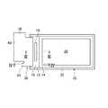
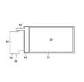
図1は、本発明の実施形態に係る液晶表示装置の表面図である。図2は、本発明の実施形態に係る液晶表示装置の裏面図である。図3は、図1に示す液晶表示装置のIII−III線断面図である。図4は、図1に示す液晶表示装置のIV−IV線断面図である。 FIG. 1 is a surface view of a liquid crystal display device according to an embodiment of the present invention. FIG. 2 is a rear view of the liquid crystal display device according to the embodiment of the present invention. 3 is a cross-sectional view taken along the line III-III of the liquid crystal display device shown in FIG. 4 is a cross-sectional view taken along line IV-IV of the liquid crystal display device shown in FIG.
液晶表示装置は、液晶表示パネル10を有する。液晶表示パネル10は、一対の基板12,14(いずれも例えばガラス基板)を有し、両者間には図示しない液晶が介在する。一方の基板12は、図示しない薄膜トランジスタ、画素電極及び配線などを含むTFT(Thin Film Transistor)基板(又はアレイ基板)であり、他方の基板14はカラーフィルタ基板である。 The liquid crystal display device includes a liquid
液晶表示パネル10の一方の基板12は、他方の基板14から突出する突出部16を有している。液晶表示パネル10(詳しくは突出部16)には、液晶を駆動するためのドライバ回路を内蔵する集積回路チップ18が搭載されている。液晶表示パネル10の一対の基板12,14には、それぞれ、偏光板20が貼り付けられている。 One
液晶表示装置は、エッジライト方式のバックライト22を有する。バックライト22は、導光板24を含む。導光板24は、液晶表示パネル10と重なるように配置される。導光板24の表面は、液晶表示パネル10の裏面に対向している。導光板24は、液晶表示パネル10の裏面側で液晶表示パネル10の端部の下方を避けて配置される。 The liquid crystal display device has an edge
液晶表示パネル10と導光板24の間には光学シート群26が配置されている。光学シート群26は、拡散シート及びプリズムシートなどを含む。また、導光板24の下(光学シート群26とは反対側)には反射シート28が配置されている。 An
バックライト22は、複数の発光部品30(図4参照)を含む。発光部品30は、例えば発光ダイオードである。発光部品30は、導光板24に光を導入するための点光源である。点光源からの光が導光板24で面光源に変換されて液晶表示パネル10に照射される。複数の発光部品30は、導光板24の端面に対向するように一列に並んで配置される(図5参照)。 The
バックライト22は、例えば樹脂からなるフレーム32を含む。フレーム32は、導光板24を内側に収納している。フレーム32に液晶表示パネル10が取り付けられている。フレーム32は、枠状の形状を有し、枠の内側のスペースを覆うように枠の一方の面に液晶表示パネル10が貼り付けられている。フレーム32は、液晶表示パネル10の裏面の周縁部に貼り付けられる。その貼り付けには、遮光性の両面テープ34が使用されている。液晶表示パネル10の端部を裏面側でフレーム32が支持している。 The
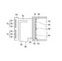
図5は、図4に示す液晶表示装置のV−V線断面図である。図6は、液晶表示装置の裏面をフレキシブル配線基板の屈曲した部分を展開して示す図である。 FIG. 5 is a cross-sectional view taken along the line VV of the liquid crystal display device shown in FIG. FIG. 6 is a diagram showing the rear surface of the liquid crystal display device with the bent portion of the flexible wiring board developed.
複数の発光部品30は、フレキシブル配線基板36に搭載されている。フレキシブル配線基板36は、屈曲して、液晶表示パネル10の表示側の面からその裏面に回り込むようになっている。フレキシブル配線基板36は、図6に示すように基板38を有する。基板38は、本体部40を有する。本体部40には図示しない電子部品が搭載される。本体部40の端部は、図1に示すように液晶表示パネル10(詳しくは突出部16)に取り付けられて電気的に接続される。本体部40は、液晶表示パネル10から離れる方向に延びる。 The plurality of
基板38は、延長部42を有する。延長部42は、液晶表示パネル10の幅方向に沿った左右いずれかの方向に偏った位置で、本体部40から、液晶表示パネル10に取り付けられる端部とは反対方向に延びる。 The
基板38は、部品搭載部44を有する。部品搭載部44は、液晶表示パネル10に取り付けられる端部とは反対方向に位置する。部品搭載部44は、液晶表示パネル10の幅方向に沿って延びる。部品搭載部44の長さは、液晶表示パネル10の幅方向に沿った左右方向の長さである。部品搭載部44の幅は、部品搭載部44の長さに直交する方向の幅である。部品搭載部44は、延長部42に接続される。延長部42は、本体部40との接続部との対向位置からずれて部品搭載部44に接続する。 The
部品搭載部44の発光部品30が搭載される面は、図4に示すように、液晶表示パネル10を向くように配置される。複数の発光部品30は、図6に示すように、部品搭載部44の長さに沿った方向に一列で並ぶ。 The surface on which the
図5又は図6に示すように、フレーム32は、導光板24に対向する内周面から窪むとともに液晶表示パネル10とは反対の面からも窪む複数の凹部46を有する。隣同士の凹部46の間には相対的に凸部48が形成されている。複数のグループの発光部品30は、それぞれ、複数の凹部46に収納される。 As shown in FIG. 5 or FIG. 6, the
図7は、複数の発光部品の接続を示す図である。複数の発光部品30は、複数グループG1,G2の発光部品30を含む。グループG1,G2のそれぞれは、隣同士が直列接続された2つ以上の発光部品30から構成される。同じグループG1又はG2では、隣同士の発光部品30のアノード電極50及びカソード電極52が接続される。隣同士の異なるグループG1,G2の隣り合う発光部品30は、直列接続されずに間隔をあけて配置されている。異なるグループG1,G2では、隣同士の発光部品30のアノード電極50及びカソード電極52が接続されない。FIG. 7 is a diagram illustrating connection of a plurality of light emitting components. The plurality of
フレキシブル配線基板36は、複数の発光部品30と電気的に接続する配線パターン54を有する。配線パターン54は、各グループG1又はG2の発光部品30を直列接続する。配線パターン54は、隣同士の異なるグループG1,G2の隣り合う発光部品30を直列接続しない。The
同じグループG1又はG2の隣り合う発光部品30は、隣同士の異なるグループG1,G2の隣り合う発光部品30の間隔よりも接近して配置されている(図5及び図6参照)。1つのグループG1,G2の発光部品30が、フレーム32の1つの凹部46に収納される。隣同士の異なるグループG1,G2の隣り合う発光部品30の間に凸部48が位置する。Adjacent
フレキシブル配線基板36は、フレーム32の液晶表示パネル10とは反対の面に重ねられる。フレキシブル配線基板36とフレーム32とは、両面テープ56によって固定されている。両面テープ56の一部は、フレーム32の凸部48とフレキシブル配線基板36の間に介在する。 The
本実施形態によれば、フレーム32には凹部46の間に凸部48が形成されるので、フレーム32の強度の低下を抑えて液晶表示パネル10の破損を防止することができる。凸部48は、直列接続されないのでショートを避けるために間隔をあけて配置された発光部品30の間に形成するので、スペースを有効的に活用することができる。 According to the present embodiment, since the
図8は、本実施形態の変形例1を示す図である。上記実施形態(図5参照)では、複数の発光部品30を2つのグループG1,G2に分けてあるが、図8に示すように、複数の発光部品130を3つのグループG1,G2,G3に分けてもよい。その場合、凸部148が2個所に形成される。FIG. 8 is a diagram illustrating a first modification of the present embodiment. In the above embodiment (see FIG. 5), but are divided into a plurality of
図9は、本実施形態の変形例2を示す図である。上記実施形態(図5参照)では、複数の発光部品30が偶数個からなる。これに対して、図9の例では、複数の発光部品230は、奇数個からなり、複数グループG1,G2の発光部品230と、いずれのグループにも属さない1つの発光部品230と、からなる。詳しくは、隣同士のグループG1,G2の発光部品230の間に、いずれのグループに属さない1つの発光部品230が配置されている。そして、いずれのグループにも属さない1つの発光部品230を挟むように凸部248が形成されている。FIG. 9 is a diagram illustrating a second modification of the present embodiment. In the said embodiment (refer FIG. 5), the some
本発明は、上述した実施形態に限定されるものではなく種々の変形が可能である。例えば、実施形態で説明した構成は、実質的に同一の構成、同一の作用効果を奏する構成又は同一の目的を達成することができる構成で置き換えることができる。 The present invention is not limited to the above-described embodiments, and various modifications can be made. For example, the configuration described in the embodiment can be replaced with substantially the same configuration, a configuration that exhibits the same operational effects, or a configuration that can achieve the same purpose.
10 液晶表示パネル、12 基板、14 基板、16 突出部、18 集積回路チップ、20 偏光板、22 バックライト、24 導光板、26 光学シート群、28 反射シート、30 発光部品、32 フレーム、34 両面テープ、36 フレキシブル配線基板、38 基板、40 本体部、42 延長部、44 部品搭載部、46 凹部、48 凸部、50 アノード電極、52 カソード電極、54 配線パターン、56 両面テープ、130 発光部品、148 凸部、230 発光部品、248 凸部、G1,G2,G3 グループ。DESCRIPTION OF
Claims (4)
Translated fromJapaneseエッジライト方式のバックライトと、
を有し、
前記バックライトは、前記液晶表示パネルと重なるように配置される導光板と、前記導光板の端面に対向するように一列に並んで配置される複数の発光部品と、前記導光板を内側に収納して前記液晶表示パネルの裏面の周縁部に貼り付けられるフレームと、を含み、
前記複数の発光部品は、隣同士が直列接続された2つ以上の前記発光部品から各グループが構成される複数グループの前記発光部品を含み、
隣同士の異なるグループの隣り合う前記発光部品は、直列接続されずに間隔をあけて配置され、
同じグループの隣り合う前記発光部品は、隣同士の異なるグループの隣り合う前記発光部品の前記間隔よりも接近して配置され、
前記フレームは、前記導光板に対向する内周面から窪むとともに前記液晶表示パネルとは反対の面からも窪む複数の凹部を有し、隣同士の前記凹部の間には相対的に凸部が形成され、
1つのグループの前記発光部品が1つの前記凹部に収納されるように、前記複数のグループの前記発光部品は、それぞれ、前記複数の凹部に収納され、
隣同士の異なるグループの隣り合う前記発光部品の間に前記凸部が位置することを特徴とする液晶表示装置。A liquid crystal display panel;
Edge-light type backlight,
Have
The backlight includes a light guide plate arranged to overlap the liquid crystal display panel, a plurality of light emitting components arranged in a row so as to face an end surface of the light guide plate, and the light guide plate stored inside And a frame attached to the peripheral edge of the back surface of the liquid crystal display panel,
The plurality of light-emitting components include a plurality of groups of the light-emitting components in which each group is composed of two or more light-emitting components adjacent to each other in series.
The adjacent light emitting components of different groups adjacent to each other are arranged at intervals without being connected in series,
The adjacent light emitting components of the same group are arranged closer to the interval between the adjacent light emitting components of different groups adjacent to each other,
The frame has a plurality of recesses recessed from an inner peripheral surface facing the light guide plate and also recessed from a surface opposite to the liquid crystal display panel, and a relatively convex portion between the adjacent recesses. Formed,
The light emitting components of the plurality of groups are respectively accommodated in the plurality of recesses, so that the light emitting components of one group are accommodated in the one recess.
The liquid crystal display device, wherein the convex portion is located between the adjacent light emitting components of different groups adjacent to each other.
前記複数の発光部品を搭載するフレキシブル配線基板をさらに有し、
前記フレキシブル配線基板は、前記フレームの前記液晶表示パネルとは反対の前記面に重ねられることを特徴とする液晶表示装置。The liquid crystal display device according to claim 1,
A flexible wiring board on which the plurality of light emitting components are mounted;
The flexible wiring board is overlaid on the surface of the frame opposite to the liquid crystal display panel.
前記フレキシブル配線基板と前記フレームとを固定する両面テープをさらに有し、
前記両面テープの一部は、前記フレームの前記凸部と前記フレキシブル配線基板の間に介在することを特徴とする液晶表示装置。The liquid crystal display device according to claim 2,
It further has a double-sided tape for fixing the flexible wiring board and the frame,
A part of the double-sided tape is interposed between the convex part of the frame and the flexible wiring board.
前記フレキシブル配線基板は、前記複数の発光部品と電気的に接続する配線パターンを有し、
前記配線パターンは、各グループの前記発光部品を直列接続し、隣同士の異なるグループの隣り合う前記発光部品を直列接続しないことを特徴とする液晶表示装置。The liquid crystal display device according to claim 2 or 3,
The flexible wiring board has a wiring pattern electrically connected to the plurality of light emitting components,
The said wiring pattern connects the said light emitting components of each group in series, and does not connect the said adjacent light emitting components of a different group adjacent to each other in series.
Priority Applications (2)
| Application Number | Priority Date | Filing Date | Title |
|---|---|---|---|
| JP2012189871AJP2014048385A (en) | 2012-08-30 | 2012-08-30 | Liquid crystal display device |
| US14/010,700US20140063415A1 (en) | 2012-08-30 | 2013-08-27 | Liquid crystal display device |
Applications Claiming Priority (1)
| Application Number | Priority Date | Filing Date | Title |
|---|---|---|---|
| JP2012189871AJP2014048385A (en) | 2012-08-30 | 2012-08-30 | Liquid crystal display device |
Publications (1)
| Publication Number | Publication Date |
|---|---|
| JP2014048385Atrue JP2014048385A (en) | 2014-03-17 |
Family
ID=50187122
Family Applications (1)
| Application Number | Title | Priority Date | Filing Date |
|---|---|---|---|
| JP2012189871APendingJP2014048385A (en) | 2012-08-30 | 2012-08-30 | Liquid crystal display device |
Country Status (2)
| Country | Link |
|---|---|
| US (1) | US20140063415A1 (en) |
| JP (1) | JP2014048385A (en) |
Families Citing this family (3)
| Publication number | Priority date | Publication date | Assignee | Title |
|---|---|---|---|---|
| CN108922407B (en)* | 2018-09-11 | 2023-11-24 | 合肥京东方光电科技有限公司 | Display screens and display devices |
| CN110910773B (en)* | 2019-07-26 | 2022-05-24 | 友达光电股份有限公司 | Display device |
| JP2023079354A (en)* | 2021-11-29 | 2023-06-08 | オムロン株式会社 | Illumination device and amusement machine equipped with the same |
Family Cites Families (13)
| Publication number | Priority date | Publication date | Assignee | Title |
|---|---|---|---|---|
| JP4489423B2 (en)* | 2003-12-26 | 2010-06-23 | シャープ株式会社 | Backlight and liquid crystal display device |
| CN101124432A (en)* | 2005-02-18 | 2008-02-13 | 美蓓亚株式会社 | planar lighting device |
| JP2008170739A (en)* | 2007-01-12 | 2008-07-24 | Hitachi Displays Ltd | Liquid crystal display |
| RU2011128719A (en)* | 2009-01-13 | 2013-02-20 | Шарп Кабусики Кайся | LIGHTING DEVICE, DISPLAY DEVICE AND TELEVISION RECEIVER |
| JP5402428B2 (en)* | 2009-09-09 | 2014-01-29 | オムロン株式会社 | Surface light source device and liquid crystal display device |
| WO2011042999A1 (en)* | 2009-10-07 | 2011-04-14 | シャープ株式会社 | Light source module and electronic apparatus provided with same |
| CN102597616B (en)* | 2009-11-12 | 2014-05-07 | 夏普株式会社 | Illuminating device, display device, and television receiver |
| CN102741608B (en)* | 2010-02-02 | 2014-10-29 | 夏普株式会社 | Lighting device, display device, and television reception device |
| TWI408460B (en)* | 2010-02-24 | 2013-09-11 | Au Optronics Corp | Optoelectronic device, display and back light module |
| US20120307523A1 (en)* | 2010-02-25 | 2012-12-06 | Sharp Kabushiki Kaisha | Light source device and display device |
| KR20110108588A (en)* | 2010-03-29 | 2011-10-06 | 삼성전자주식회사 | Display device and backlight unit |
| US8801260B2 (en)* | 2011-07-11 | 2014-08-12 | Seiko Epson Corporation | Display device, electronic apparatus and lighting device |
| US20130128189A1 (en)* | 2011-11-21 | 2013-05-23 | Chechang Hu | Backlight Module and Liquid Crystal Display Device |
- 2012
- 2012-08-30JPJP2012189871Apatent/JP2014048385A/enactivePending
- 2013
- 2013-08-27USUS14/010,700patent/US20140063415A1/ennot_activeAbandoned
Also Published As
| Publication number | Publication date |
|---|---|
| US20140063415A1 (en) | 2014-03-06 |
Similar Documents
| Publication | Publication Date | Title |
|---|---|---|
| JP5236767B2 (en) | Liquid crystal display | |
| JP5255960B2 (en) | Liquid crystal display | |
| JP4831789B2 (en) | Backlight unit | |
| US9063362B2 (en) | Display apparatus | |
| CN103091900B (en) | Liquid crystal indicator | |
| JP2010060866A (en) | Electro-optical panel, electro-optical device, and electronic equipment | |
| US10851979B2 (en) | Backlight lamp bar, backlight module and display device | |
| CN109782466B (en) | display device | |
| JP5426456B2 (en) | Liquid crystal display | |
| KR102614911B1 (en) | Liquid crystal display device and LED assembly | |
| JP2014048385A (en) | Liquid crystal display device | |
| KR20180071614A (en) | Liquid crystal display device | |
| KR20160084534A (en) | Liquid crystal display device | |
| JP2009244499A (en) | Liquid crystal display | |
| JP2014085545A (en) | Liquid crystal display device | |
| US8625042B2 (en) | Display device | |
| JP5273553B2 (en) | Liquid crystal display | |
| KR101325459B1 (en) | Liquid crystal display device | |
| KR20170117701A (en) | Liquid Crystal Display Device | |
| JP5718846B2 (en) | Liquid crystal display | |
| JP2008107701A (en) | Liquid crystal display | |
| JP4692458B2 (en) | Surface lighting device | |
| JP2007127962A (en) | Liquid crystal display device | |
| WO2013008742A1 (en) | Display device and television reception device | |
| JP2012079418A (en) | Light source device, liquid crystal display and flexible printed circuit board |