JP2014042004A - Semiconductor device and manufacturing method of the same - Google Patents
Semiconductor device and manufacturing method of the sameDownload PDFInfo
- Publication number
- JP2014042004A JP2014042004AJP2013146057AJP2013146057AJP2014042004AJP 2014042004 AJP2014042004 AJP 2014042004AJP 2013146057 AJP2013146057 AJP 2013146057AJP 2013146057 AJP2013146057 AJP 2013146057AJP 2014042004 AJP2014042004 AJP 2014042004A
- Authority
- JP
- Japan
- Prior art keywords
- film
- insulating film
- oxide
- oxide semiconductor
- nitrogen
- Prior art date
- Legal status (The legal status is an assumption and is not a legal conclusion. Google has not performed a legal analysis and makes no representation as to the accuracy of the status listed.)
- Withdrawn
Links
Images


Classifications
- H—ELECTRICITY
- H10—SEMICONDUCTOR DEVICES; ELECTRIC SOLID-STATE DEVICES NOT OTHERWISE PROVIDED FOR
- H10D—INORGANIC ELECTRIC SEMICONDUCTOR DEVICES
- H10D30/00—Field-effect transistors [FET]
- H10D30/60—Insulated-gate field-effect transistors [IGFET]
- H10D30/67—Thin-film transistors [TFT]
- H10D30/674—Thin-film transistors [TFT] characterised by the active materials
- H10D30/6755—Oxide semiconductors, e.g. zinc oxide, copper aluminium oxide or cadmium stannate
- H—ELECTRICITY
- H01—ELECTRIC ELEMENTS
- H01L—SEMICONDUCTOR DEVICES NOT COVERED BY CLASS H10
- H01L21/00—Processes or apparatus adapted for the manufacture or treatment of semiconductor or solid state devices or of parts thereof
- H01L21/02—Manufacture or treatment of semiconductor devices or of parts thereof
- H01L21/02104—Forming layers
- H01L21/02107—Forming insulating materials on a substrate
- H01L21/02225—Forming insulating materials on a substrate characterised by the process for the formation of the insulating layer
- H01L21/0226—Forming insulating materials on a substrate characterised by the process for the formation of the insulating layer formation by a deposition process
- H01L21/02263—Forming insulating materials on a substrate characterised by the process for the formation of the insulating layer formation by a deposition process deposition from the gas or vapour phase
- H01L21/02271—Forming insulating materials on a substrate characterised by the process for the formation of the insulating layer formation by a deposition process deposition from the gas or vapour phase deposition by decomposition or reaction of gaseous or vapour phase compounds, i.e. chemical vapour deposition
- H01L21/02274—Forming insulating materials on a substrate characterised by the process for the formation of the insulating layer formation by a deposition process deposition from the gas or vapour phase deposition by decomposition or reaction of gaseous or vapour phase compounds, i.e. chemical vapour deposition in the presence of a plasma [PECVD]
- H—ELECTRICITY
- H01—ELECTRIC ELEMENTS
- H01L—SEMICONDUCTOR DEVICES NOT COVERED BY CLASS H10
- H01L21/00—Processes or apparatus adapted for the manufacture or treatment of semiconductor or solid state devices or of parts thereof
- H01L21/02—Manufacture or treatment of semiconductor devices or of parts thereof
- H01L21/04—Manufacture or treatment of semiconductor devices or of parts thereof the devices having potential barriers, e.g. a PN junction, depletion layer or carrier concentration layer
- H01L21/18—Manufacture or treatment of semiconductor devices or of parts thereof the devices having potential barriers, e.g. a PN junction, depletion layer or carrier concentration layer the devices having semiconductor bodies comprising elements of Group IV of the Periodic Table or AIIIBV compounds with or without impurities, e.g. doping materials
- H01L21/26—Bombardment with radiation
- H01L21/263—Bombardment with radiation with high-energy radiation
- H01L21/265—Bombardment with radiation with high-energy radiation producing ion implantation
- H—ELECTRICITY
- H01—ELECTRIC ELEMENTS
- H01L—SEMICONDUCTOR DEVICES NOT COVERED BY CLASS H10
- H01L21/00—Processes or apparatus adapted for the manufacture or treatment of semiconductor or solid state devices or of parts thereof
- H01L21/02—Manufacture or treatment of semiconductor devices or of parts thereof
- H01L21/04—Manufacture or treatment of semiconductor devices or of parts thereof the devices having potential barriers, e.g. a PN junction, depletion layer or carrier concentration layer
- H01L21/18—Manufacture or treatment of semiconductor devices or of parts thereof the devices having potential barriers, e.g. a PN junction, depletion layer or carrier concentration layer the devices having semiconductor bodies comprising elements of Group IV of the Periodic Table or AIIIBV compounds with or without impurities, e.g. doping materials
- H01L21/30—Treatment of semiconductor bodies using processes or apparatus not provided for in groups H01L21/20 - H01L21/26
- H01L21/324—Thermal treatment for modifying the properties of semiconductor bodies, e.g. annealing, sintering
- H—ELECTRICITY
- H10—SEMICONDUCTOR DEVICES; ELECTRIC SOLID-STATE DEVICES NOT OTHERWISE PROVIDED FOR
- H10D—INORGANIC ELECTRIC SEMICONDUCTOR DEVICES
- H10D30/00—Field-effect transistors [FET]
- H10D30/01—Manufacture or treatment
- H10D30/021—Manufacture or treatment of FETs having insulated gates [IGFET]
- H—ELECTRICITY
- H10—SEMICONDUCTOR DEVICES; ELECTRIC SOLID-STATE DEVICES NOT OTHERWISE PROVIDED FOR
- H10D—INORGANIC ELECTRIC SEMICONDUCTOR DEVICES
- H10D30/00—Field-effect transistors [FET]
- H10D30/60—Insulated-gate field-effect transistors [IGFET]
- H10D30/67—Thin-film transistors [TFT]
- H10D30/6704—Thin-film transistors [TFT] having supplementary regions or layers in the thin films or in the insulated bulk substrates for controlling properties of the device
Landscapes
- Engineering & Computer Science (AREA)
- Physics & Mathematics (AREA)
- Power Engineering (AREA)
- Condensed Matter Physics & Semiconductors (AREA)
- General Physics & Mathematics (AREA)
- Manufacturing & Machinery (AREA)
- Computer Hardware Design (AREA)
- Microelectronics & Electronic Packaging (AREA)
- Chemical & Material Sciences (AREA)
- High Energy & Nuclear Physics (AREA)
- Chemical Kinetics & Catalysis (AREA)
- Toxicology (AREA)
- Health & Medical Sciences (AREA)
- Plasma & Fusion (AREA)
- Thin Film Transistor (AREA)
- Crystallography & Structural Chemistry (AREA)
- Materials Engineering (AREA)
- Mechanical Engineering (AREA)
- Metallurgy (AREA)
- Organic Chemistry (AREA)
- Solid State Image Pick-Up Elements (AREA)
- Liquid Crystal (AREA)
- Electroluminescent Light Sources (AREA)
Abstract
Translated fromJapaneseDescription
Translated fromJapanese本発明は、電界効果トランジスタを有する半導体装置及びその作製方法に関する。 The present invention relates to a semiconductor device having a field effect transistor and a manufacturing method thereof.
液晶表示装置や発光表示装置に代表されるフラットパネルディスプレイの多くに用いられているトランジスタは、ガラス基板上に形成されたアモルファスシリコン、単結晶シリコンまたは多結晶シリコンなどのシリコン半導体によって構成されている。また、該シリコン半導体を用いたトランジスタは、集積回路(IC)などにも利用されている。 Transistors used in many flat panel displays typified by liquid crystal display devices and light-emitting display devices are composed of silicon semiconductors such as amorphous silicon, single crystal silicon, or polycrystalline silicon formed on a glass substrate. . In addition, a transistor including the silicon semiconductor is used for an integrated circuit (IC) or the like.
近年、シリコン半導体に代わって、半導体特性を示す金属酸化物をトランジスタに用いる技術が注目されている。なお、本明細書では、半導体特性を示す金属酸化物を酸化物半導体とよぶことにする。 In recent years, a technique using a metal oxide exhibiting semiconductor characteristics for a transistor instead of a silicon semiconductor has attracted attention. Note that in this specification, a metal oxide exhibiting semiconductor characteristics is referred to as an oxide semiconductor.
例えば、酸化物半導体として、酸化亜鉛、またはIn−Ga−Zn系酸化物を用いたトランジスタを作製し、該トランジスタを表示装置の画素のスイッチング素子などに用いる技術が開示されている(特許文献1及び特許文献2参照)。 For example, a technique is disclosed in which a transistor using zinc oxide or an In—Ga—Zn-based oxide as an oxide semiconductor is manufactured, and the transistor is used for a switching element of a pixel of a display device or the like (Patent Document 1). And Patent Document 2).
ところで、特に酸化物半導体においては、水素がキャリアの供給源となることが指摘されている。そのため、酸化物半導体の形成時に水素が混入しないような措置を講じることが求められており、酸化物半導体膜や、酸化物半導体膜に接するゲート絶縁膜の水素を低減することで、しきい値電圧の変動を抑制している(特許文献3参照)。 Incidentally, it has been pointed out that hydrogen is a carrier supply source particularly in an oxide semiconductor. Therefore, it is required to take measures so that hydrogen does not enter during formation of the oxide semiconductor. By reducing hydrogen in the oxide semiconductor film and the gate insulating film in contact with the oxide semiconductor film, a threshold value is obtained. Voltage fluctuation is suppressed (see Patent Document 3).
ところで、窒素は水素と同様にキャリア供給源となる。このため、窒素が酸化物半導体膜に侵入すると、酸化物半導体膜のキャリア密度が増加し、酸化物半導体膜を有するトランジスタの電気特性の変動、代表的にはしきい値電圧のマイナスシフトが生じる。また、トランジスタごとに電気特性がばらつくという問題がある。 By the way, nitrogen becomes a carrier supply source like hydrogen. Therefore, when nitrogen enters the oxide semiconductor film, the carrier density of the oxide semiconductor film increases, resulting in a change in electrical characteristics of the transistor including the oxide semiconductor film, typically a minus shift in threshold voltage. . In addition, there is a problem that electric characteristics vary from transistor to transistor.
また、酸化物半導体膜を有するトランジスタ上に保護膜として絶縁膜を設ける場合、酸化物半導体膜との界面準位を低減するため、酸化絶縁膜を設けることが好ましい。しかしながら、当該酸化絶縁膜に窒素が含まれると、酸化絶縁膜に欠陥が含まれてしまう。当該欠陥により、酸化物半導体膜を有するトランジスタの電気特性において、経時変化やバイアス温度ストレス試験(以下、BT(Bias−Temperature)ストレス試験ともいう。)により、トランジスタの電気特性の変動量、代表的にはしきい値電圧の変動量が増大してしまうという問題がある。また、異なるドレイン電圧において、オン電流の立ち上がりゲート電圧(Vg)が異なってしまうという問題がある。 In the case where an insulating film is provided as a protective film over a transistor including an oxide semiconductor film, an oxide insulating film is preferably provided in order to reduce the interface state with the oxide semiconductor film. However, when nitrogen is included in the oxide insulating film, the oxide insulating film includes defects. Due to the defects, in the electrical characteristics of the transistor including an oxide semiconductor film, the amount of change in electrical characteristics of the transistor due to aging or a bias temperature stress test (hereinafter also referred to as a BT (Bias-Temperature) stress test), However, there is a problem that the fluctuation amount of the threshold voltage increases. Further, there is a problem that the rising gate voltage (Vg) of the on-current is different at different drain voltages.
また、酸化物半導体膜を有するトランジスタ上にプラズマCVD法により保護膜として絶縁膜を設ける場合、酸化物半導体膜にプラズマダメージが入り、酸化物半導体膜に欠陥が形成されてしまう。酸化物半導体膜に含まれる欠陥の一つとして酸素欠損があるが、酸素欠損が含まれている酸化物半導体膜を用いたトランジスタは、酸化物半導体膜を有するトランジスタの電気特性の変動、代表的にはしきい値電圧のマイナスシフトが生じるという問題がある。 Further, in the case where an insulating film is provided as a protective film over a transistor including an oxide semiconductor film by a plasma CVD method, plasma damage enters the oxide semiconductor film, and defects are formed in the oxide semiconductor film. One of defects included in an oxide semiconductor film is oxygen deficiency. A transistor including an oxide semiconductor film including oxygen deficiency is a typical variation in electrical characteristics of a transistor including an oxide semiconductor film. Has a problem that a negative shift of the threshold voltage occurs.
そこで、本発明の一態様は、酸化物半導体膜を有するトランジスタにおいて、酸化物半導体膜へ移動する窒素量を低減すると共に、当該トランジスタ上に形成される酸化絶縁膜の窒素量を低減することを課題の一とする。また、本発明の一態様は、酸化物半導体膜を有するトランジスタを用いた半導体装置において、電気特性の変動を抑制すると共に、信頼性を向上させることを課題の一とする。 Thus, according to one embodiment of the present invention, in a transistor including an oxide semiconductor film, the amount of nitrogen transferred to the oxide semiconductor film is reduced and the amount of nitrogen in the oxide insulating film formed over the transistor is reduced. One of the issues. Another object of one embodiment of the present invention is to suppress variation in electrical characteristics and improve reliability in a semiconductor device including a transistor including an oxide semiconductor film.
本発明の一態様は、チャネル領域が形成される酸化物半導体膜を有するトランジスタ上に、窒素を有する酸化絶縁膜を形成した後、加熱処理を行って、窒素を有する酸化絶縁膜から窒素を放出させることを特徴とする半導体装置の作製方法である。 In one embodiment of the present invention, after an oxide insulating film including nitrogen is formed over a transistor including an oxide semiconductor film in which a channel region is formed, heat treatment is performed, so that nitrogen is released from the oxide insulating film including nitrogen. A method for manufacturing a semiconductor device.
上記加熱処理温度は、窒素を有する酸化絶縁膜から窒素を放出させる温度であり、代表的には、150℃以上500℃以下である。 The heat treatment temperature is a temperature at which nitrogen is released from the oxide insulating film containing nitrogen, and is typically 150 ° C. or higher and 500 ° C. or lower.
また、本発明の一態様は、チャネル領域が形成される酸化物半導体膜を有するトランジスタと、該トランジスタ上に形成される窒素を有する酸化絶縁膜とを有し、窒素を有する酸化絶縁膜の窒素濃度は、二次イオン質量分析法(SIMS:Secondary Ion Mass Spectrometry)の検出下限以上3×10²⁰atoms/cm3未満、好ましくは1×1018atoms/cm3以上1×1020atoms/cm3以下であることを特徴とする半導体装置である。One embodiment of the present invention includes a transistor including an oxide semiconductor film in which a channel region is formed and an oxide insulating film including nitrogen formed over the transistor, and nitrogen in the oxide insulating film including nitrogen. The concentration is not less than the detection lower limit of secondary ion mass spectrometry (SIMS) and less than 3 × 10²⁰ atoms / cm3 , preferably 1 × 10¹⁸ atoms /
なお、窒素を有する酸化絶縁膜は、化学量論的組成を満たす酸素よりも多くの酸素を含んでいてもよい。窒素を有する酸化絶縁膜をプラズマCVD法で形成する場合、原料ガスとしては、シリコンを含む堆積性気体と、酸化性気体として一酸化二窒素、二酸化窒素等の窒素酸化物とを用いることで、酸化反応が促進され、化学量論的組成を満たす酸素よりも多くの酸素を有する膜、代表的には窒素を有する酸化絶縁膜を形成することができる。 Note that the oxide insulating film containing nitrogen may contain more oxygen than oxygen that satisfies the stoichiometric composition. When forming an oxide insulating film having nitrogen by a plasma CVD method, as a source gas, a deposition gas containing silicon and a nitrogen oxide such as dinitrogen monoxide and nitrogen dioxide as an oxidizing gas are used. An oxidation reaction is promoted, and a film having more oxygen than that in the stoichiometric composition, typically an oxide insulating film having nitrogen, can be formed.
また、チャネル領域が形成される酸化物半導体膜上に、シリコンを含む堆積性気体と、酸化性気体とを用いたプラズマCVD法により、酸化絶縁膜を形成する場合、酸化性気体として一酸化二窒素、二酸化窒素等の窒素酸化物を用いることで、酸化物半導体膜へのダメージを低減しつつ、酸化絶縁膜、代表的には窒素を有する酸化絶縁膜を形成することができる。 In the case where an oxide insulating film is formed over an oxide semiconductor film in which a channel region is formed by a plasma CVD method using a deposition gas containing silicon and an oxidation gas, dioxide monoxide is used as the oxidation gas. By using nitrogen oxide such as nitrogen or nitrogen dioxide, an oxide insulating film, typically an oxide insulating film containing nitrogen, can be formed while reducing damage to the oxide semiconductor film.
チャネル領域が形成される酸化物半導体膜を有するトランジスタ上に、窒素を有する酸化絶縁膜を形成した後、加熱処理を行うことで、窒素を有する酸化絶縁膜から窒素を放出させることが可能であり、加熱処理された窒素を有する酸化絶縁膜の窒素濃度が、SIMSの検出下限以上3×10²⁰atoms/cm3未満、好ましくは1×1018atoms/cm3以上1×1020atoms/cm3以下となる。この結果、酸化物半導体膜に移動する窒素量を低減することが可能である。Nitrogen can be released from the oxide insulating film containing nitrogen by performing heat treatment after the oxide insulating film containing nitrogen is formed over the transistor including the oxide semiconductor film in which the channel region is formed. Further, the nitrogen concentration of the heat-treated nitrogen-containing oxide insulating film is equal to or higher than the detection limit of SIMS and lower than 3 × 10²⁰ atoms / cm3 , preferably 1 × 10¹⁸ atoms /
本発明の一態様により、チャネル領域が形成される酸化物半導体膜を有するトランジスタの電気特性の変動を抑制すると共に、信頼性を向上させることができる。 According to one embodiment of the present invention, variation in electrical characteristics of a transistor including an oxide semiconductor film in which a channel region is formed can be suppressed and reliability can be improved.
以下では、本発明の実施の形態について図面を用いて詳細に説明する。ただし、本発明は以下の説明に限定されず、本発明の趣旨及びその範囲から逸脱することなくその形態及び詳細を様々に変更し得ることは、当業者であれば容易に理解される。従って、本発明は、以下に示す実施の形態及び実施例の記載内容に限定して解釈されるものではない。また、以下に説明する実施の形態及び実施例において、同一部分または同様の機能を有する部分には、同一の符号または同一のハッチパターンを異なる図面間で共通して用い、その繰り返しの説明は省略する。 Hereinafter, embodiments of the present invention will be described in detail with reference to the drawings. However, the present invention is not limited to the following description, and it will be easily understood by those skilled in the art that modes and details can be variously changed without departing from the spirit and scope of the present invention. Therefore, the present invention should not be construed as being limited to the description of the embodiments and examples below. In the following embodiments and examples, the same portions or portions having similar functions are denoted by the same reference numerals or the same hatch patterns in different drawings, and description thereof is not repeated. To do.
なお、本明細書で説明する各図において、各構成の大きさ、膜の厚さ、または領域は、明瞭化のために誇張されている場合がある。よって、必ずしもそのスケールに限定されない。 Note that in each drawing described in this specification, the size, the film thickness, or the region of each component is exaggerated for clarity in some cases. Therefore, it is not necessarily limited to the scale.
また、本明細書にて用いる第1、第2、第3などの用語は、構成要素の混同を避けるために付したものであり、数的に限定するものではない。そのため、例えば、「第1の」を「第2の」または「第3の」などと適宜置き換えて説明することができる。 Further, the terms such as first, second, and third used in this specification are given for avoiding confusion between components, and are not limited numerically. Therefore, for example, the description can be made by appropriately replacing “first” with “second” or “third”.
また、「ソース」や「ドレイン」の機能は、回路動作において電流の方向が変化する場合などには入れ替わることがある。このため、本明細書においては、「ソース」や「ドレイン」の用語は、入れ替えて用いることができるものとする。 Further, the functions of “source” and “drain” may be interchanged when the direction of current changes during circuit operation. Therefore, in this specification, the terms “source” and “drain” can be used interchangeably.
また、電圧とは2点間における電位差のことをいい、電位とはある一点における静電場の中にある単位電荷が持つ静電エネルギー(電気的な位置エネルギー)のことをいう。ただし、一般的に、ある一点における電位と基準となる電位(例えば接地電位)との電位差のことを、単に電位もしくは電圧と呼び、電位と電圧が同義語として用いられることが多い。このため、本明細書では特に指定する場合を除き、電位を電圧と読み替えてもよいし、電圧を電位と読み替えてもよいこととする。 Further, the voltage refers to a potential difference between two points, and the potential refers to electrostatic energy (electric potential energy) possessed by a unit charge in an electrostatic field at a certain point. However, generally, a potential difference between a potential at a certain point and a reference potential (for example, ground potential) is simply referred to as a potential or a voltage, and the potential and the voltage are often used as synonyms. Therefore, in this specification, unless otherwise specified, the potential may be read as a voltage, or the voltage may be read as a potential.
また、酸化物半導体膜を有するトランジスタはnチャネル型トランジスタであるため、本明細書において、ゲート電圧が0Vの場合、ドレイン電流が流れていないとみなすことができるトランジスタを、ノーマリーオフ特性を有するトランジスタと定義する。また、ゲート電圧が0Vの場合、ドレイン電流が流れているとみなすことができるトランジスタを、ノーマリーオン特性を有するトランジスタと定義する。 In addition, since a transistor including an oxide semiconductor film is an n-channel transistor, in this specification, a transistor that can be regarded as having no drain current flowing when the gate voltage is 0 V has normally-off characteristics. It is defined as a transistor. A transistor that can be regarded as having a drain current flowing when the gate voltage is 0 V is defined as a transistor having normally-on characteristics.
(実施の形態1)
本実施の形態では、本発明の一態様である半導体装置、及びその作製方法について図面を参照して説明する。(Embodiment 1)
In this embodiment, a semiconductor device which is one embodiment of the present invention and a manufacturing method thereof will be described with reference to drawings.
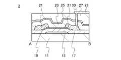
図1(A)及び図1(B)に、半導体装置が有するトランジスタ1の上面図及び断面図を示す。図1(A)はトランジスタ1の上面図であり、図1(B)は、図1(A)の一点鎖線A−B間の断面図である。なお、図1(A)では、明瞭化のため、基板11、ゲート絶縁膜17、窒素を有する酸化絶縁膜23などを省略している。 1A and 1B are a top view and a cross-sectional view of a
図1(A)及び図1(B)に示すトランジスタ1は、基板11上に設けられるゲート電極15と、基板11及びゲート電極15上に形成されるゲート絶縁膜17と、ゲート絶縁膜17を介して、ゲート電極15と重なる酸化物半導体膜19と、酸化物半導体膜19に接する一対の電極21とを有する。また、ゲート絶縁膜17、酸化物半導体膜19、及び一対の電極21上には、窒素を有する酸化絶縁膜23が形成される。 A
本実施の形態に示すトランジスタ1上に設けられる窒素を有する酸化絶縁膜23は、二次イオン質量分析法(SIMS:Secondary Ion Mass Spectrometry)により得られる窒素濃度が、SIMS検出下限以上3×10²⁰atoms/cm3未満、好ましくは1×1018atoms/cm3以上1×1020atoms/cm3以下である。窒素を有する酸化絶縁膜23に含まれる窒素量が少ないため、トランジスタ1に含まれる酸化物半導体膜19への窒素の移動量が少ない。また、窒素を有する酸化絶縁膜の欠陥量が少ない。In the
なお、窒素を有する酸化絶縁膜23は、実施の形態2で説明する化学量論的組成を満たす酸素よりも多くの酸素を有する酸化絶縁膜としてもよい。 Note that the
酸化物半導体膜19に窒素が含まれると、酸化物半導体膜19において、キャリアである電子が生じ、キャリア密度が増加し、n型化しやすい。この結果、酸化物半導体膜19を有するトランジスタはノーマリーオン特性となりやすい。これらのため、酸化物半導体膜19上に設けられる窒素を有する酸化絶縁膜23の窒素の濃度を、SIMS検出下限以上3×10²⁰atoms/cm3未満、好ましくは1×1018atoms/cm3以上1×1020atoms/cm3以下とすることで、酸化物半導体膜19へ侵入する窒素量を減らすことが可能である。このため、酸化物半導体膜19の窒素量を減らすことにより、しきい値電圧のマイナスシフトを抑制することができると共に、電気特性のばらつきを低減することができる。また、トランジスタのソース及びドレインにおけるリーク電流を、代表的には、オフ電流を低減することが可能である。また、窒素を有する酸化絶縁膜23の窒素濃度を低減することで、窒素を有する酸化絶縁膜23の欠陥量、特に、酸化物半導体膜19及び窒素を有する酸化絶縁膜23の界面の欠陥量、並びに窒素を有する酸化絶縁膜23において酸化物半導体膜19近傍の欠陥量を低減することが可能であり、トランジスタの電気特性の変動量を低減すると共に、異なるドレイン電圧において、オン電流の立ち上がりゲート電圧(Vg)を略同一とすることができる。When nitrogen is contained in the
窒素を有する酸化絶縁膜23は、酸化物半導体膜19との界面特性を向上させるため、上記濃度の窒素が含まれている酸化絶縁膜を用いることが好ましい。窒素を有する酸化絶縁膜23としては、厚さ150nm以上400nm以下の、窒素を有する酸化シリコン(酸化窒化シリコンと記載する場合もある。)、窒素を有する酸化アルミニウム(酸化窒化アルミニウムと記載する場合もある。)、窒素を有する酸化ハフニウム(酸化窒化ハフニウムと記載する場合もある。)、窒素を有する酸化ガリウム(酸化窒化ガリウムと記載する場合もある。)、または窒素を有するGa−Zn系金属酸化物等を用いることができる。 The
なお、本明細書において、酸化窒化シリコン膜とは、その組成として、窒素よりも酸素の含有量が多い膜を指し、窒化酸化シリコン膜とは、その組成として、酸素よりも窒素の含有量が多い膜を指す。また、酸化窒化アルミニウム膜、酸化窒化ハフニウム膜、酸化窒化ガリウム膜、窒化酸化アルミニウム膜、窒化酸化ハフニウム膜、窒化酸化ガリウム膜に関しても、窒素と酸素の含有量の関係は、酸化窒化シリコン膜と、窒化酸化シリコン膜と同様である。 Note that in this specification, a silicon oxynitride film refers to a film having a higher oxygen content than nitrogen as a composition, and a silicon nitride oxide film has a nitrogen content as compared to oxygen as a composition. Refers to many membranes. In addition, regarding the aluminum oxynitride film, the hafnium oxynitride film, the gallium oxynitride film, the aluminum nitride oxide film, the hafnium nitride oxide film, and the gallium nitride oxide film, the relationship between the content of nitrogen and oxygen is as follows: This is similar to the silicon nitride oxide film.
以下に、トランジスタ1の他の構成の詳細について説明する。 The details of another configuration of the
基板11の材質などに大きな制限はないが、少なくとも、後の熱処理に耐えうる程度の耐熱性を有している必要がある。例えば、ガラス基板、セラミック基板、石英基板、サファイア基板等を、基板11として用いてもよい。また、シリコンや炭化シリコンなどの単結晶半導体基板、多結晶半導体基板、シリコンゲルマニウム等の化合物半導体基板、SOI(Silicon On Insulator)基板等を適用することも可能であり、これらの基板上に半導体素子が設けられたものを、基板11として用いてもよい。 Although there is no big restriction | limiting in the material etc. of the board |
また、基板11として、可撓性基板を用い、可撓性基板上に直接、トランジスタ1を形成してもよい。または、基板11とトランジスタ1の間に剥離層を設けてもよい。剥離層は、その上に半導体装置を一部あるいは全部完成させた後、基板11より分離し、他の基板に転載するのに用いることができる。その際、トランジスタ1は耐熱性の劣る基板や可撓性の基板にも転載できる。 Alternatively, a flexible substrate may be used as the
なお、基板11及びゲート電極15の間に下地絶縁膜を設けてもよい。下地絶縁膜としては、酸化シリコン、酸化窒化シリコン、窒化シリコン、窒化酸化シリコン、酸化ガリウム、酸化ハフニウム、酸化イットリウム、酸化アルミニウム、酸化窒化アルミニウム等がある。なお、下地絶縁膜として、窒化シリコン、酸化ガリウム、酸化ハフニウム、酸化イットリウム、酸化アルミニウム等を用いることで、基板11から不純物、代表的にはアルカリ金属、水、水素等の酸化物半導体膜19への拡散を抑制することができる。 Note that a base insulating film may be provided between the
ゲート電極15は、アルミニウム、クロム、銅、タンタル、チタン、モリブデン、タングステンから選ばれた金属元素、または上述した金属元素を成分とする合金か、上述した金属元素を組み合わせた合金等を用いて形成することができる。また、マンガン、ジルコニウムのいずれか一または複数から選択された金属元素を用いてもよい。また、ゲート電極15は、単層構造でも、二層以上の積層構造としてもよい。例えば、シリコンを含むアルミニウム膜の単層構造、アルミニウム膜上にチタン膜を積層する二層構造、窒化チタン膜上にチタン膜を積層する二層構造、窒化チタン膜上にタングステン膜を積層する二層構造、窒化タンタル膜または窒化タングステン膜上にタングステン膜を積層する二層構造、チタン膜と、そのチタン膜上にアルミニウム膜を積層し、さらにその上にチタン膜を形成する三層構造等がある。また、アルミニウムに、チタン、タンタル、タングステン、モリブデン、クロム、ネオジム、スカンジウムから選ばれた元素の膜、または複数組み合わせた合金膜、もしくは窒化膜を用いてもよい。 The
また、ゲート電極15は、インジウム錫酸化物、酸化タングステンを含むインジウム酸化物、酸化タングステンを含むインジウム亜鉛酸化物、酸化チタンを含むインジウム酸化物、酸化チタンを含むインジウム錫酸化物、インジウム亜鉛酸化物、酸化シリコンを添加したインジウム錫酸化物等の透光性を有する導電性材料を適用することもできる。また、上記透光性を有する導電性材料と、上記金属元素の積層構造とすることもできる。 The
また、ゲート電極15とゲート絶縁膜17との間に、In−Ga−Zn系酸窒化物膜、In−Sn系酸窒化物膜、In−Ga系酸窒化物膜、In−Zn系酸窒化物膜、Sn系酸窒化物膜、In系酸窒化物膜、金属窒化膜(InN、ZnN等)等を設けてもよい。これらの膜は5eV以上、好ましくは5.5eV以上の仕事関数を有し、酸化物半導体の電子親和力よりも大きい値であるため、酸化物半導体を用いたトランジスタのしきい値電圧をプラスにシフトすることができ、所謂ノーマリーオフ特性のスイッチング素子を実現できる。例えば、In−Ga−Zn系酸窒化物膜を用いる場合、少なくとも酸化物半導体膜19より高い窒素濃度、具体的には7原子%以上のIn−Ga−Zn系酸窒化物膜を用いる。 Further, an In—Ga—Zn-based oxynitride film, an In—Sn-based oxynitride film, an In—Ga-based oxynitride film, and an In—Zn-based oxynitride are provided between the
ゲート絶縁膜17は、例えば酸化シリコン、酸化窒化シリコン、窒化酸化シリコン、窒化シリコン、酸化アルミニウム、酸化ハフニウム、酸化ガリウムまたはGa−Zn系金属酸化物などを用いればよく、積層または単層で設ける。なお、酸化物半導体膜19との界面特性を向上させるため、ゲート絶縁膜17において少なくとも酸化物半導体膜19と接する領域は酸化絶縁膜で形成することが好ましい。 The
また、ゲート絶縁膜17に、酸素、水素、水等のブロッキング効果を有する絶縁膜を設けることで、酸化物半導体膜19からの酸素の外部への拡散と、外部から酸化物半導体膜19への水素、水等の侵入を防ぐことができる。酸素、水素、水等のブロッキング効果を有する絶縁膜としては、酸化アルミニウム、酸化窒化アルミニウム、酸化ガリウム、酸化窒化ガリウム、酸化イットリウム、酸化窒化イットリウム、酸化ハフニウム、酸化窒化ハフニウム、窒化シリコン等がある。 Further, by providing the
また、ゲート絶縁膜17として、ハフニウムシリケート(HfSiOx)、窒素を有するハフニウムシリケート(HfSixOyNz)、窒素を有するハフニウムアルミネート(HfAlxOyNz)、酸化ハフニウム、酸化イットリウムなどのhigh−k材料を用いることでトランジスタのゲートリークを低減できる。Further, as the
また、ゲート絶縁膜17を積層構造とし、第1の窒化シリコン膜として、欠陥量が少ない窒化シリコン膜とし、第2の窒化シリコン膜として、第1の窒化シリコン膜上に、水素脱離量及びアンモニア脱離量の少ない窒化シリコン膜を設け、第2の窒化シリコン膜上に、上記ゲート絶縁膜17で羅列した酸化絶縁膜のいずれかを設けることが好ましい。第2の窒化シリコン膜としては、昇温脱離ガス分析法において、水素分子の脱離量が5×10²¹分子/cm3未満、好ましくは3×1021分子/cm3以下、さらに好ましくは1×1021分子/cm3以下であり、アンモニア分子の脱離量が1×1022分子/cm3未満、好ましくは5×1021分子/cm3以下、さらに好ましくは1×1021分子/cm3以下である窒化絶縁膜を用いることが好ましい。上記第1の窒化シリコン膜及び第2の窒化シリコン膜をゲート絶縁膜17の一部として用いることで、ゲート絶縁膜17として、欠陥量が少なく、且つ水素及びアンモニアの脱離量の少ないゲート絶縁膜を形成することができる。この結果、ゲート絶縁膜17に含まれる水素及び窒素の、酸化物半導体膜19への移動量を低減することが可能である。In addition, the
酸化物半導体を用いたトランジスタにおいて、酸化物半導体膜及びゲート絶縁膜の界面またはゲート絶縁膜に捕獲準位(界面準位ともいう。)があると、トランジスタのしきい値電圧の変動、代表的にはしきい値電圧のマイナスシフト、及びトランジスタがオン状態となるときにドレイン電流が一桁変化するのに必要なゲート電圧を示すサブスレッショルド係数(S値)の増大の原因となる。この結果、トランジスタごとに電気特性がばらつくという問題がある。このため、ゲート絶縁膜17として、欠陥量の少ない窒化シリコン膜を用いることで、また、酸化物半導体膜19と接する領域に酸化絶縁膜を設けることで、しきい値電圧のマイナスシフトを抑制すると共に、S値の増大を抑制することができる。 In a transistor including an oxide semiconductor, if there is a trap level (also referred to as an interface level) at the interface between the oxide semiconductor film and the gate insulating film or the gate insulating film, variation in the threshold voltage of the transistor, This causes a negative shift of the threshold voltage and an increase in the subthreshold coefficient (S value) indicating the gate voltage necessary for the drain current to change by an order of magnitude when the transistor is turned on. As a result, there is a problem that electric characteristics vary from transistor to transistor. Therefore, a negative shift of the threshold voltage is suppressed by using a silicon nitride film with a small amount of defects as the
ゲート絶縁膜17の厚さは、5nm以上400nm以下、より好ましくは10nm以上300nm以下、より好ましくは50nm以上250nm以下とするとよい。 The thickness of the
酸化物半導体膜19は、少なくともインジウム(In)若しくは亜鉛(Zn)を含むことが好ましい。または、InとZnの双方を含むことが好ましい。また、該酸化物半導体を用いたトランジスタの電気特性のばらつきを減らすため、それらと共に、スタビライザーの一または複数を有することが好ましい。 The
スタビライザーとしては、ガリウム(Ga)、スズ(Sn)、ハフニウム(Hf)、アルミニウム(Al)、またはジルコニウム(Zr)等がある。また、他のスタビライザーとしては、ランタノイドである、ランタン(La)、セリウム(Ce)、プラセオジム(Pr)、ネオジム(Nd)、サマリウム(Sm)、ユウロピウム(Eu)、ガドリニウム(Gd)、テルビウム(Tb)、ジスプロシウム(Dy)、ホルミウム(Ho)、エルビウム(Er)、ツリウム(Tm)、イッテルビウム(Yb)、ルテチウム(Lu)等がある。 Examples of the stabilizer include gallium (Ga), tin (Sn), hafnium (Hf), aluminum (Al), and zirconium (Zr). Other stabilizers include lanthanoids such as lanthanum (La), cerium (Ce), praseodymium (Pr), neodymium (Nd), samarium (Sm), europium (Eu), gadolinium (Gd), terbium (Tb). ), Dysprosium (Dy), holmium (Ho), erbium (Er), thulium (Tm), ytterbium (Yb), lutetium (Lu), and the like.
例えば、酸化物半導体として、酸化インジウム、酸化スズ、酸化亜鉛、二元系金属酸化物であるIn−Zn系金属酸化物、Sn−Zn系金属酸化物、Al−Zn系金属酸化物、Zn−Mg系金属酸化物、Sn−Mg系金属酸化物、In−Mg系金属酸化物、In−Ga系金属酸化物、In−W系金属酸化物、三元系金属酸化物であるIn−Ga−Zn系金属酸化物(IGZOとも表記する)、In−Al−Zn系金属酸化物、In−Sn−Zn系金属酸化物、Sn−Ga−Zn系金属酸化物、Al−Ga−Zn系金属酸化物、Sn−Al−Zn系金属酸化物、In−Hf−Zn系金属酸化物、In−La−Zn系金属酸化物、In−Ce−Zn系金属酸化物、In−Pr−Zn系金属酸化物、In−Nd−Zn系金属酸化物、In−Sm−Zn系金属酸化物、In−Eu−Zn系金属酸化物、In−Gd−Zn系金属酸化物、In−Tb−Zn系金属酸化物、In−Dy−Zn系金属酸化物、In−Ho−Zn系金属酸化物、In−Er−Zn系金属酸化物、In−Tm−Zn系金属酸化物、In−Yb−Zn系金属酸化物、In−Lu−Zn系金属酸化物、四元系金属酸化物であるIn−Sn−Ga−Zn系金属酸化物、In−Hf−Ga−Zn系金属酸化物、In−Al−Ga−Zn系金属酸化物、In−Sn−Al−Zn系金属酸化物、In−Sn−Hf−Zn系金属酸化物、In−Hf−Al−Zn系金属酸化物を用いることができる。 For example, as an oxide semiconductor, indium oxide, tin oxide, zinc oxide, binary metal oxides In—Zn metal oxide, Sn—Zn metal oxide, Al—Zn metal oxide, Zn— Mg-based metal oxide, Sn-Mg-based metal oxide, In-Mg-based metal oxide, In-Ga-based metal oxide, In-W-based metal oxide, ternary metal oxide, In-Ga- Zn-based metal oxide (also expressed as IGZO), In-Al-Zn-based metal oxide, In-Sn-Zn-based metal oxide, Sn-Ga-Zn-based metal oxide, Al-Ga-Zn-based metal oxide Sn-Al-Zn metal oxide, In-Hf-Zn metal oxide, In-La-Zn metal oxide, In-Ce-Zn metal oxide, In-Pr-Zn metal oxide , In-Nd-Zn-based metal oxide, In-Sm-Z Metal oxide, In-Eu-Zn metal oxide, In-Gd-Zn metal oxide, In-Tb-Zn metal oxide, In-Dy-Zn metal oxide, In-Ho-Zn Metal oxide, In-Er-Zn metal oxide, In-Tm-Zn metal oxide, In-Yb-Zn metal oxide, In-Lu-Zn metal oxide, quaternary metal oxide In-Sn-Ga-Zn-based metal oxide, In-Hf-Ga-Zn-based metal oxide, In-Al-Ga-Zn-based metal oxide, In-Sn-Al-Zn-based metal oxide In-Sn-Hf-Zn-based metal oxide and In-Hf-Al-Zn-based metal oxide can be used.
なお、ここで、例えば、In−Ga−Zn系金属酸化物とは、InとGaとZnを主成分として有する酸化物という意味であり、InとGaとZnの比率は問わない。また、InとGaとZn以外の金属元素が入っていてもよい。 Note that here, for example, an In—Ga—Zn-based metal oxide means an oxide containing In, Ga, and Zn as its main components, and there is no limitation on the ratio of In, Ga, and Zn. Moreover, metal elements other than In, Ga, and Zn may be contained.
また、酸化物半導体として、InMO3(ZnO)m(m>0、且つ、mは整数でない)で表記される材料を用いてもよい。なお、Mは、Ga、Fe、Mn及びCoから選ばれた一の金属元素または複数の金属元素を示す。また、酸化物半導体として、In2SnO5(ZnO)n(n>0、且つ、nは整数)で表記される材料を用いてもよい。Alternatively, a material represented by InMO3 (ZnO)m (m> 0 is satisfied, and m is not an integer) may be used as the oxide semiconductor. Note that M represents one metal element or a plurality of metal elements selected from Ga, Fe, Mn, and Co. Alternatively, a material represented by In2 SnO5 (ZnO)n (n> 0 is satisfied, and n is an integer) may be used as the oxide semiconductor.
例えば、In:Ga:Zn=1:1:1(=1/3:1/3:1/3)、In:Ga:Zn=2:2:1(=2/5:2/5:1/5)、あるいはIn:Ga:Zn=3:1:2(=1/2:1/6:1/3)の原子数比のIn−Ga−Zn系金属酸化物を用いることができる。あるいは、In:Sn:Zn=1:1:1(=1/3:1/3:1/3)、In:Sn:Zn=2:1:3(=1/3:1/6:1/2)あるいはIn:Sn:Zn=2:1:5(=1/4:1/8:5/8)の原子数比のIn−Sn−Zn系金属酸化物を用いるとよい。なお、金属酸化物の原子数比は、誤差として上記の原子数比のプラスマイナス20%の変動を含む。 For example, In: Ga: Zn = 1: 1: 1 (= 1/3: 1/3: 1/3), In: Ga: Zn = 2: 2: 1 (= 2/5: 2/5: 1) / 5), or an In—Ga—Zn-based metal oxide with an atomic ratio of In: Ga: Zn = 3: 1: 2 (= 1/2: 1/6: 1/3) can be used. Alternatively, In: Sn: Zn = 1: 1: 1 (= 1/3: 1/3: 1/3), In: Sn: Zn = 2: 1: 3 (= 1/3: 1/6: 1) / 2) or In: Sn: Zn = 2: 1: 5 (= 1/4: 1/8: 5/8) atomic ratio In—Sn—Zn-based metal oxide may be used. Note that the atomic ratio of the metal oxide includes a variation of plus or minus 20% of the above atomic ratio as an error.
しかし、これらに限られず、必要とする半導体特性及び電気特性(電界効果移動度、しきい値電圧等)に応じて適切な組成のものを用いればよい。また、必要とする半導体特性を得るために、キャリア密度や不純物濃度、欠陥密度、金属元素と酸素の原子数比、原子間距離、密度等を適切なものとすることが好ましい。 However, the composition is not limited thereto, and a material having an appropriate composition may be used depending on required semiconductor characteristics and electrical characteristics (field effect mobility, threshold voltage, and the like). In order to obtain the required semiconductor characteristics, it is preferable that the carrier density, impurity concentration, defect density, atomic ratio of metal element to oxygen, interatomic distance, density, and the like are appropriate.
例えば、In−Sn−Zn系金属酸化物では比較的容易に高い移動度が得られる。しかしながら、In−Ga−Zn系金属酸化物でも、バルク内欠陥密度を低くすることにより移動度を上げることができる。 For example, high mobility can be obtained relatively easily with an In—Sn—Zn-based metal oxide. However, mobility can be increased by reducing the defect density in the bulk also in the case of using an In—Ga—Zn-based metal oxide.
また、酸化物半導体膜19に形成することが可能な金属酸化物は、エネルギーギャップが2eV以上、好ましくは2.5eV以上、より好ましくは3eV以上である。このように、エネルギーギャップの広い酸化物半導体を用いることで、トランジスタのオフ電流を低減することができる。 The metal oxide that can be formed in the
また、酸化物半導体膜19は、非晶質構造、単結晶構造、または多結晶構造であってもよい。 The
また、酸化物半導体膜19として、結晶化部分を有するCAAC−OS(C Axis Aligned Crystalline Oxide Semiconductorともいう。)膜を用いてもよい。 The
CAAC−OS膜は、複数の結晶部を有する酸化物半導体膜の一つであり、ほとんどの結晶部は、一辺が100nm未満の立方体内に収まる大きさである。従って、CAAC−OS膜に含まれる結晶部は、一辺が10nm未満、5nm未満または3nm未満の立方体内に収まる大きさの場合も含まれる。CAAC−OS膜は、微結晶酸化物半導体膜よりも欠陥準位密度が低いという特徴がある。以下、CAAC−OS膜について詳細な説明を行う。 The CAAC-OS film is one of oxide semiconductor films having a plurality of crystal parts, and most of the crystal parts are large enough to fit in a cube whose one side is less than 100 nm. Therefore, the case where a crystal part included in the CAAC-OS film fits in a cube whose one side is less than 10 nm, less than 5 nm, or less than 3 nm is included. The CAAC-OS film is characterized by having a lower density of defect states than a microcrystalline oxide semiconductor film. Hereinafter, the CAAC-OS film is described in detail.
CAAC−OS膜を透過型電子顕微鏡(TEM:Transmission Electron Microscope)によって観察すると、結晶部同士の明確な境界、即ち結晶粒界(グレインバウンダリーともいう。)を確認することができない。そのため、CAAC−OS膜は、粒界に起因する電子移動度の低下が起こりにくいといえる。 When the CAAC-OS film is observed with a transmission electron microscope (TEM), a clear boundary between crystal parts, that is, a grain boundary (also referred to as a grain boundary) cannot be confirmed. Therefore, it can be said that the CAAC-OS film is unlikely to decrease in electron mobility due to grain boundaries.
CAAC−OS膜を、試料面と概略平行な方向からTEMによって観察(断面TEM観察)すると、結晶部において、金属原子が層状に配列していることを確認できる。金属原子の各層は、CAAC−OS膜の膜を形成する面(被形成面ともいう。)または上面の凹凸を反映した形状であり、CAAC−OS膜の被形成面または上面と平行に配列する。 When the CAAC-OS film is observed by TEM (cross-sectional TEM observation) from a direction substantially parallel to the sample surface, it can be confirmed that metal atoms are arranged in layers in the crystal part. Each layer of metal atoms has a shape reflecting unevenness of a surface (also referred to as a formation surface) or an upper surface on which the CAAC-OS film is formed, and is arranged in parallel with the formation surface or the upper surface of the CAAC-OS film. .
なお、本明細書において、「平行」とは、二つの直線が−10°以上10°以下の角度で配置されている状態をいう。従って、−5°以上5°以下の場合も含まれる。また、「垂直」とは、二つの直線が80°以上100°以下の角度で配置されている状態をいう。従って、85°以上95°以下の場合も含まれる。 In this specification, “parallel” refers to a state in which two straight lines are arranged at an angle of −10 ° to 10 °. Therefore, the case of −5 ° to 5 ° is also included. “Vertical” refers to a state in which two straight lines are arranged at an angle of 80 ° to 100 °. Therefore, the case of 85 ° to 95 ° is also included.
一方、CAAC−OS膜を、試料面と概略垂直な方向からTEMによって観察(平面TEM観察)すると、結晶部において、金属原子が三角形状または六角形状に配列していることを確認できる。しかしながら、異なる結晶部間で、金属原子の配列に規則性は見られない。 On the other hand, when the CAAC-OS film is observed by TEM (planar TEM observation) from a direction substantially perpendicular to the sample surface, it can be confirmed that metal atoms are arranged in a triangular shape or a hexagonal shape in the crystal part. However, there is no regularity in the arrangement of metal atoms between different crystal parts.
断面TEM観察および平面TEM観察より、CAAC−OS膜の結晶部は配向性を有していることがわかる。 From the cross-sectional TEM observation and the planar TEM observation, it is found that the crystal part of the CAAC-OS film has orientation.
CAAC−OS膜に対し、X線回折(XRD:X−Ray Diffraction)装置を用いて構造解析を行うと、例えばInGaZnO4の結晶を有するCAAC−OS膜のout−of−plane法による解析では、回折角(2θ)が31°近傍にピークが現れる場合がある。このピークは、InGaZnO4の結晶の(009)面に帰属されることから、CAAC−OS膜の結晶がc軸配向性を有し、c軸が被形成面または上面に概略垂直な方向を向いていることが確認できる。When structural analysis is performed on a CAAC-OS film using an X-ray diffraction (XRD) apparatus, for example, in the analysis of a CAAC-OS film having an InGaZnO4 crystal by an out-of-plane method, A peak may appear when the diffraction angle (2θ) is around 31 °. Since this peak is attributed to the (009) plane of the InGaZnO4 crystal, the CAAC-OS film crystal has c-axis orientation, and the c-axis is in a direction substantially perpendicular to the formation surface or the top surface. Can be confirmed.
一方、CAAC−OS膜に対し、c軸に概略垂直な方向からX線を入射させるin−plane法による解析では、2θが56°近傍にピークが現れる場合がある。このピークは、InGaZnO4の結晶の(110)面に帰属される。InGaZnO4の単結晶酸化物半導体膜であれば、2θを56°近傍に固定し、試料面の法線ベクトルを軸(φ軸)として試料を回転させながら分析(φスキャン)を行うと、(110)面と等価な結晶面に帰属されるピークが6本観察される。これに対し、CAAC−OS膜の場合は、2θを56°近傍に固定してφスキャンした場合でも、明瞭なピークが現れない。On the other hand, when the CAAC-OS film is analyzed by an in-plane method in which X-rays are incident from a direction substantially perpendicular to the c-axis, a peak may appear when 2θ is around 56 °. This peak is attributed to the (110) plane of the InGaZnO4 crystal. In the case of a single crystal oxide semiconductor film of InGaZnO4 , when 2θ is fixed in the vicinity of 56 ° and analysis (φ scan) is performed while rotating the sample with the normal vector of the sample surface as the axis (φ axis), Six peaks attributed to the crystal plane equivalent to the (110) plane are observed. On the other hand, in the case of a CAAC-OS film, a peak is not clearly observed even when φ scan is performed with 2θ fixed at around 56 °.
以上のことから、CAAC−OS膜では、異なる結晶部間ではa軸およびb軸の配向は不規則であるが、c軸配向性を有し、かつc軸が被形成面または上面の法線ベクトルに平行な方向を向いていることがわかる。従って、前述の断面TEM観察で確認された層状に配列した金属原子の各層は、結晶のab面に平行な面である。 From the above, in the CAAC-OS film, the orientation of the a-axis and the b-axis is irregular between different crystal parts, but the c-axis is aligned, and the c-axis is a normal line of the formation surface or the top surface. It can be seen that the direction is parallel to the vector. Therefore, each layer of metal atoms arranged in a layer shape confirmed by the above-mentioned cross-sectional TEM observation is a plane parallel to the ab plane of the crystal.
なお、結晶部は、CAAC−OS膜を成膜した際、または加熱処理などの結晶化処理を行った際に形成される。上述したように、結晶のc軸は、CAAC−OS膜の被形成面または上面の法線ベクトルに平行な方向に配向する。従って、例えば、CAAC−OS膜の形状をエッチングなどによって変化させた場合、結晶のc軸がCAAC−OS膜の被形成面または上面の法線ベクトルと平行にならないこともある。 Note that the crystal part is formed when a CAAC-OS film is formed or when crystallization treatment such as heat treatment is performed. As described above, the c-axis of the crystal is oriented in a direction parallel to the normal vector of the formation surface or the top surface of the CAAC-OS film. Therefore, for example, when the shape of the CAAC-OS film is changed by etching or the like, the c-axis of the crystal may not be parallel to the normal vector of the formation surface or the top surface of the CAAC-OS film.
また、CAAC−OS膜中の結晶化度が均一でなくてもよい。例えば、CAAC−OS膜の結晶部が、CAAC−OS膜の上面近傍からの結晶成長によって形成される場合、上面近傍の領域は、被形成面近傍の領域よりも結晶化度が高くなることがある。また、CAAC−OS膜に不純物を添加する場合、不純物が添加された領域の結晶化度が変化し、部分的に結晶化度の異なる領域が形成されることもある。 Further, the crystallinity in the CAAC-OS film is not necessarily uniform. For example, in the case where the crystal part of the CAAC-OS film is formed by crystal growth from the vicinity of the top surface of the CAAC-OS film, the region near the top surface can have a higher degree of crystallinity than the region near the formation surface. is there. In addition, in the case where an impurity is added to the CAAC-OS film, the crystallinity of a region to which the impurity is added changes, and a region having a different degree of crystallinity may be formed.
なお、InGaZnO4の結晶を有するCAAC−OS膜のout−of−plane法による解析では、2θが31°近傍のピークの他に、2θが36°近傍にもピークが現れる場合がある。2θが36°近傍のピークは、CAAC−OS膜中の一部に、c軸配向性を有さない結晶が含まれることを示している。CAAC−OS膜は、2θが31°近傍にピークを示し、2θが36°近傍にピークを示さないことが好ましい。Note that when the CAAC-OS film including an InGaZnO4 crystal is analyzed by an out-of-plane method, a peak may also appear when 2θ is around 36 ° in addition to the peak where 2θ is around 31 °. A peak at 2θ of around 36 ° indicates that a crystal having no c-axis alignment is included in part of the CAAC-OS film. The CAAC-OS film preferably has a peak at 2θ of around 31 ° and no peak at 2θ of around 36 °.
また、CAAC−OS膜を用いたトランジスタは、可視光や紫外光の照射による電気特性の変動が小さい。 In addition, a transistor including a CAAC-OS film has little variation in electrical characteristics due to irradiation with visible light or ultraviolet light.
また、酸化物半導体膜19は、複数の酸化物半導体膜が積層された構造でもよい。例えば、酸化物半導体膜19を、第1の酸化物半導体膜と第2の酸化物半導体膜の積層として、第1の酸化物半導体膜と第2の酸化物半導体膜に、異なる組成の金属酸化物を用いてもよい。例えば、第1の酸化物半導体膜に二元系金属酸化物乃至四元系金属酸化物の一を用い、第2の酸化物半導体膜に第1の酸化物半導体膜と異なる二元系金属酸化物乃至四元系金属酸化物を用いてもよい。 The
また、第1の酸化物半導体膜と第2の酸化物半導体膜の構成元素を同一とし、両者の構成元素の原子数比を異ならせてもよい。例えば、第1の酸化物半導体膜の原子数比をIn:Ga:Zn=1:1:1とし、第2の酸化物半導体膜の原子数比をIn:Ga:Zn=3:1:2としてもよい。また、第1の酸化物半導体膜の原子数比をIn:Ga:Zn=1:3:2とし、第2の酸化物半導体膜の原子数比をIn:Ga:Zn=2:1:3としてもよい。なお、各酸化物半導体膜の金属元素の原子数比は、誤差として上記の原子数比のプラスマイナス20%の変動を含む。 Alternatively, the constituent elements of the first oxide semiconductor film and the second oxide semiconductor film may be the same, and the atomic ratio of the constituent elements may be different. For example, the atomic ratio of the first oxide semiconductor film is In: Ga: Zn = 1: 1: 1, and the atomic ratio of the second oxide semiconductor film is In: Ga: Zn = 3: 1: 2. It is good. The atomic ratio of the first oxide semiconductor film is In: Ga: Zn = 1: 3: 2, and the atomic ratio of the second oxide semiconductor film is In: Ga: Zn = 2: 1: 3. It is good. Note that the atomic ratio of metal elements in each oxide semiconductor film includes a variation of plus or minus 20% of the above atomic ratio as an error.
この時、第1の酸化物半導体膜と第2の酸化物半導体膜のうち、ゲート電極に近い側(チャネル側)の酸化物半導体膜のInとGaの含有率をIn>Gaとするとよい。またゲート電極から遠い側(バックチャネル側)の酸化物半導体膜のInとGaの含有率をIn≦Gaとするとよい。 At this time, the In and Ga contents in the oxide semiconductor film on the side close to the gate electrode (channel side) of the first oxide semiconductor film and the second oxide semiconductor film are preferably In> Ga. The content ratio of In and Ga in the oxide semiconductor film far from the gate electrode (back channel side) is preferably In ≦ Ga.
また、酸化物半導体膜19を3層構造とし、第1の酸化物半導体膜〜第3の酸化物半導体膜の構成元素を同一とし、且つそれぞれの構成元素の原子数比を異ならせてもよい。例えば、第1の酸化物半導体膜の原子数比をIn:Ga:Zn=1:3:2とし、第2の酸化物半導体膜の原子数比をIn:Ga:Zn=3:1:2とし、第3の酸化物半導体膜の原子数比をIn:Ga:Zn=1:1:1としてもよい。 Alternatively, the
Ga及びZnよりInの原子数比が小さい酸化物半導体膜、代表的には原子数比がIn:Ga:Zn=1:3:2である第1の酸化物半導体膜は、Ga及びZnよりInの原子数比が大きい酸化物半導体膜、代表的には第2の酸化物半導体膜、並びにGa、Zn、及びInの原子数比が同じ酸化物半導体膜、代表的には第3の酸化物半導体膜と比較して、酸素欠損が生じにくいため、キャリア密度が増加することを抑制することができる。 An oxide semiconductor film in which the atomic ratio of In is smaller than that of Ga and Zn, typically, the first oxide semiconductor film in which the atomic ratio is In: Ga: Zn = 1: 3: 2 is higher than that of Ga and Zn. An oxide semiconductor film having a large In atomic ratio, typically a second oxide semiconductor film, and an oxide semiconductor film having the same atomic ratio of Ga, Zn, and In, typically a third oxide Since oxygen vacancies are less likely to occur compared to a physical semiconductor film, an increase in carrier density can be suppressed.
また、第1の酸化物半導体膜〜第3の酸化物半導体膜の構成元素は同一であるため、第1の酸化物半導体膜は、第2の酸化物半導体膜との界面におけるトラップ準位が少ない。このため、酸化物半導体膜19を上記構造とすることで、トランジスタの経時変化や光BTストレス試験によるしきい値電圧の変動量を低減することができる。 In addition, since the constituent elements of the first oxide semiconductor film to the third oxide semiconductor film are the same, the first oxide semiconductor film has a trap level at the interface with the second oxide semiconductor film. Few. Therefore, when the
酸化物半導体では主として重金属のs軌道がキャリア伝導に寄与しており、Inの含有率を多くすることにより、より多くのs軌道が重なるため、In>Gaの組成となる酸化物はIn≦Gaの組成となる酸化物と比較して高いキャリア移動度を備える。また、GaはInと比較して酸素欠損の形成エネルギーが大きく酸素欠損が生じにくいため、In≦Gaの組成となる酸化物はIn>Gaの組成となる酸化物と比較して安定した特性を備える。 In oxide semiconductors, s orbitals of heavy metals mainly contribute to carrier conduction, and by increasing the In content, more s orbitals overlap. Therefore, an oxide having a composition of In> Ga has In ≦ Ga. Compared with the oxide which becomes the composition, it has a high carrier mobility. In addition, since Ga has a larger energy generation energy of oxygen deficiency than In, and oxygen deficiency is less likely to occur, an oxide having a composition of In ≦ Ga has stable characteristics compared to an oxide having a composition of In> Ga. Prepare.
チャネル側にIn>Gaの組成となる酸化物半導体を適用し、バックチャネル側にIn≦Gaの組成となる酸化物半導体を適用することで、トランジスタの電界効果移動度及び信頼性をさらに高めることが可能となる。 By applying an oxide semiconductor having a composition of In> Ga to the channel side and applying an oxide semiconductor having a composition of In ≦ Ga to the back channel side, the field-effect mobility and reliability of the transistor can be further increased. Is possible.
また、第1の酸化物半導体膜乃至第3の酸化物半導体膜に、結晶性の異なる酸化物半導体を適用してもよい。すなわち、単結晶酸化物半導体、多結晶酸化物半導体、非晶質酸化物半導体、またはCAAC−OSを適宜組み合わせた構成としてもよい。また、第1の酸化物半導体膜、乃至第2の酸化物半導体膜のいずれか一に非晶質酸化物半導体を適用すると、酸化物半導体膜19の内部応力や外部からの応力を緩和し、トランジスタの特性ばらつきが低減され、また、トランジスタの信頼性をさらに高めることが可能となる。 Alternatively, oxide semiconductors having different crystallinities may be used for the first oxide semiconductor film to the third oxide semiconductor film. That is, a single crystal oxide semiconductor, a polycrystalline oxide semiconductor, an amorphous oxide semiconductor, or a CAAC-OS may be combined as appropriate. In addition, when an amorphous oxide semiconductor is applied to any one of the first oxide semiconductor film and the second oxide semiconductor film, the internal stress of the
酸化物半導体膜19の厚さは、1nm以上100nm以下、更に好ましくは1nm以上50nm以下、更に好ましくは1nm以上30nm以下、更に好ましくは3nm以上20nm以下とすることが好ましい。 The thickness of the
酸化物半導体膜19において、二次イオン質量分析法により得られるアルカリ金属またはアルカリ土類金属の濃度を、1×10¹⁸atoms/cm3以下、さらに好ましくは2×1016atoms/cm3以下であることが望ましい。アルカリ金属及びアルカリ土類金属は、酸化物半導体と結合するとキャリアを生成する場合があり、トランジスタのオフ電流の上昇の原因となるためである。In the
酸化物半導体膜19に含まれる水素は、金属原子と結合する酸素と反応して水となると共に、酸素が脱離した格子(あるいは酸素が脱離した部分)には欠損が形成されてしまう。また、水素が酸素と反応することで、キャリアである電子が生じてしまう。このため、酸化物半導体膜19において、二次イオン質量分析法により得られる水素濃度を、5×10¹⁸atoms/cm3未満、好ましくは1×1018atoms/cm3以下、より好ましくは5×1017atoms/cm3以下、さらに好ましくは1×1016atoms/cm3以下とすることが好ましい。Hydrogen contained in the
酸化物半導体膜19に含まれる水素は、金属原子と結合する酸素と反応して水となると共に、酸素が脱離した格子(あるいは酸素が脱理した部分)には欠損が形成されてしまう。また、水素の一部が酸素と結合することで、キャリアである電子が生じてしまう。これらのため、酸化物半導体膜の成膜工程において、水素を含む不純物を極めて減らすことにより、酸化物半導体膜の水素濃度を低減することが可能である。このため、水素をできるだけ除去された酸化物半導体膜をチャネル領域とすることにより、しきい値電圧のマイナスシフトを抑制することができると共に、電気特性のばらつきを低減することができる。また、トランジスタのソース及びドレインにおけるリーク電流を、代表的には、オフ電流を低減することが可能である。 Hydrogen contained in the
また、酸化物半導体膜19の窒素濃度を5×10¹⁸atoms/cm3以下とすることで、トランジスタのしきい値電圧のマイナスシフトを抑制することができると共に、電気特性のばらつきを低減することができる。In addition, by setting the nitrogen concentration of the
なお、水素量をできるだけ低減することで酸化物半導体膜を高純度化することができる。高純度化された酸化物半導体膜をチャネル領域に用いたトランジスタのオフ電流が小さいことは、いろいろな実験により証明できる。例えば、チャネル幅が1×106μmでチャネル長が10μmの素子であっても、ソース電極とドレイン電極間の電圧(ドレイン電圧)が1Vから10Vの範囲において、オフ電流が、半導体パラメータアナライザの測定限界以下、すなわち1×10⁻¹³A以下という特性を得ることができる。この場合、オフ電流をトランジスタのチャネル幅で除した数値は、100zA/μm以下であることが分かる。また、容量素子とトランジスタとを接続して、容量素子に流入または容量素子から流出する電荷を当該トランジスタで制御する回路を用いて、オフ電流の測定を行った。当該測定では、上記トランジスタに高純度化された酸化物半導体膜をチャネル領域に用い、容量素子の単位時間あたりの電荷量の推移から当該トランジスタのオフ電流を測定した。その結果、トランジスタのソース電極とドレイン電極間の電圧が3Vの場合に、数十yA/μmという、さらに小さいオフ電流が得られることが分かった。従って、高純度化された酸化物半導体膜をチャネル領域に用いたトランジスタは、オフ電流が著しく小さい。Note that the oxide semiconductor film can be highly purified by reducing the amount of hydrogen as much as possible. It can be proved by various experiments that the off-state current of the transistor in which the highly purified oxide semiconductor film is used for a channel region is small. For example, even in an element having a channel width of 1 × 106 μm and a channel length of 10 μm, when the voltage between the source electrode and the drain electrode (drain voltage) is in the range of 1V to 10V, It is possible to obtain characteristics that are below the measurement limit, that is, 1 × 10⁻¹³ A or less. In this case, the numerical value obtained by dividing the off-state current by the channel width of the transistor is 100 zA / μm or less. In addition, off-state current was measured using a circuit in which a capacitor and a transistor were connected and charge flowing into or out of the capacitor was controlled by the transistor. In this measurement, a highly purified oxide semiconductor film of the transistor was used for a channel region, and the off-state current of the transistor was measured from the change in the amount of charge per unit time of the capacitor. As a result, it was found that when the voltage between the source electrode and the drain electrode of the transistor is 3 V, an even smaller off current of several tens of yA / μm can be obtained. Therefore, a transistor using a highly purified oxide semiconductor film for a channel region has extremely low off-state current.
一対の電極21は、導電材料として、アルミニウム、チタン、クロム、ニッケル、銅、イットリウム、ジルコニウム、モリブデン、銀、タンタル、またはタングステンからなる単体金属、またはこれを主成分とする合金を単層構造または積層構造として用いる。例えば、シリコンを含むアルミニウム膜の単層構造、アルミニウム膜上にチタン膜を積層する二層構造、タングステン膜上にチタン膜を積層する二層構造、銅−マグネシウム−アルミニウム合金膜上に銅膜を積層する二層構造、チタン膜または窒化チタン膜と、そのチタン膜または窒化チタン膜上に重ねてアルミニウム膜または銅膜を積層し、さらにその上にチタン膜または窒化チタン膜を形成する三層構造、モリブデン膜または窒化モリブデン膜と、そのモリブデン膜または窒化モリブデン膜上に重ねてアルミニウム膜または銅膜を積層し、さらにその上にモリブデン膜または窒化モリブデン膜を形成する三層構造等がある。なお、酸化インジウム、酸化錫または酸化亜鉛を含む透明導電材料を用いてもよい。 The pair of
なお、本実施の形態では、一対の電極21を酸化物半導体膜19及び窒素を有する酸化絶縁膜23の間に設けたが、ゲート絶縁膜17及び酸化物半導体膜19の間に設けてもよい。 Note that in this embodiment, the pair of
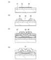
次に、図1に示すトランジスタ1の作製方法について、図2を用いて説明する。 Next, a method for manufacturing the
図2(A)に示すように、基板11上にゲート電極15を形成し、ゲート電極15上にゲート絶縁膜17を形成する。 As shown in FIG. 2A, the
ゲート電極15の形成方法を以下に示す。はじめに、スパッタリング法、CVD法、蒸着法等により導電膜を形成し、導電膜上にフォトリソグラフィ工程によりマスクを形成する。次に、該マスクを用いて導電膜の一部をエッチングして、ゲート電極15を形成する。この後、マスクを除去する。 A method for forming the
なお、ゲート電極15は、上記形成方法の代わりに、電解メッキ法、印刷法、インクジェット法等で形成してもよい。 Note that the
ここでは、厚さ100nmのタングステン膜をスパッタリング法により形成する。次に、フォトリソグラフィ工程によりマスクを形成し、当該マスクを用いてタングステン膜をドライエッチングして、ゲート電極15を形成する。 Here, a tungsten film with a thickness of 100 nm is formed by a sputtering method. Next, a mask is formed by a photolithography process, and the tungsten film is dry-etched using the mask to form the
ゲート絶縁膜17は、スパッタリング法、CVD法、蒸着法等で形成する。 The
ゲート絶縁膜17として、CVD法を用いて酸化シリコン膜または酸化窒化シリコン膜を形成する場合、原料ガスとしては、シリコンを含む堆積性気体及び酸化性気体を用いることが好ましい。シリコンを含む堆積性気体の代表例としては、シラン、ジシラン、トリシラン、フッ化シラン等がある。酸化性気体としては、酸素、オゾン、一酸化二窒素、二酸化窒素等がある。 In the case where a silicon oxide film or a silicon oxynitride film is formed as the
また、ゲート絶縁膜17として、積層構造の窒化シリコン膜及び酸化絶縁膜を形成する場合、2段階の形成方法を用いて窒化シリコン膜を積層して形成することが好ましい。はじめに、シラン、窒素、及びアンモニアの混合ガスを原料ガスとして用いたプラズマCVD法により、欠陥量の少ない第1の窒化シリコン膜を形成する。次に、シリコンを含む堆積性気体、窒素、及びアンモニアを原料ガスとして用い、アンモニアに対する窒素の流量比を10倍以上50倍以下、好ましくは20倍以上40倍以下とすることで、水素脱離量及びアンモニア脱離量の少ない窒化シリコン膜を第2の窒化シリコン膜として形成することができる。このような形成方法により、ゲート絶縁膜17として、欠陥量が少なく、且つ水素脱離量及びアンモニア脱離量の少ない窒化シリコン膜を形成することができる。 In the case where a silicon nitride film and an oxide insulating film having a stacked structure are formed as the
また、ゲート絶縁膜17として酸化ガリウム膜を形成する場合、MOCVD(Metal Organic Chemical Vapor Deposition)法を用いて形成することができる。 Further, when a gallium oxide film is formed as the
ここでは、プラズマCVD法により、厚さ300nmの第1の窒化シリコン膜、厚さ50nmの第2の窒化シリコン膜、及び厚さ50nmの酸化窒化シリコン膜を積層したゲート絶縁膜17を形成する。 Here, a
次に、図2(B)に示すように、ゲート絶縁膜17上に酸化物半導体膜19を形成する。 Next, as illustrated in FIG. 2B, the
酸化物半導体膜19の形成方法について以下に説明する。ゲート絶縁膜17上にスパッタリング法、塗布法、パルスレーザー蒸着法、レーザーアブレーション法等により酸化物半導体膜を形成する。次に、酸化物半導体膜上にフォトリソグラフィ工程によりマスクを形成した後、該マスクを用いて酸化物半導体膜の一部をエッチングすることで、図2(B)に示すように、ゲート絶縁膜17上であって、ゲート電極15の一部と重なるように素子分離された酸化物半導体膜19を形成する。この後、マスクを除去する。 A method for forming the
また、酸化物半導体膜19として印刷法を用いることで、素子分離された酸化物半導体膜19を直接形成することができる。 Further, by using a printing method for the
スパッタリング法で酸化物半導体膜を形成する場合、プラズマを発生させるための電源装置は、RF電源装置、AC電源装置、DC電源装置等を適宜用いることができる。 In the case of forming an oxide semiconductor film by a sputtering method, an RF power supply device, an AC power supply device, a DC power supply device, or the like can be used as appropriate as a power supply device for generating plasma.
スパッタリングガスは、希ガス(代表的にはアルゴン)雰囲気、酸素雰囲気、希ガス及び酸素の混合ガス雰囲気を適宜用いる。なお、希ガス及び酸素の混合ガス雰囲気の場合、希ガスに対して酸素のガス比を高めることが好ましい。 As the sputtering gas, a rare gas (typically argon) atmosphere, an oxygen atmosphere, or a mixed gas atmosphere of a rare gas and oxygen is appropriately used. Note that in the case of a mixed gas atmosphere of a rare gas and oxygen, it is preferable to increase the ratio of oxygen to rare gas.
また、ターゲットは、形成する酸化物半導体膜の組成にあわせて、適宜選択すればよい。 The target may be selected as appropriate in accordance with the composition of the oxide semiconductor film to be formed.
なお、酸化物半導体膜を形成する際に、例えば、スパッタリング法を用いる場合、基板温度を150℃以上750℃以下、好ましくは150℃以上450℃以下、さらに好ましくは200℃以上350℃以下として、酸化物半導体膜を成膜することで、CAAC−OS膜を形成することができる。 Note that when the oxide semiconductor film is formed, for example, when a sputtering method is used, the substrate temperature is 150 ° C. or higher and 750 ° C. or lower, preferably 150 ° C. or higher and 450 ° C. or lower, more preferably 200 ° C. or higher and 350 ° C. or lower. By forming the oxide semiconductor film, a CAAC-OS film can be formed.
なお、CAAC−OS膜は、例えば、多結晶である酸化物半導体スパッタリング用ターゲットを用い、スパッタリング法によって成膜する。当該スパッタリング用ターゲットにイオンが衝突すると、スパッタリング用ターゲットに含まれる結晶領域がa−b面から劈開し、a−b面に平行な面を有する平板状またはペレット状のスパッタリング粒子として剥離することがある。この場合、当該平板状のスパッタリング粒子が、結晶状態を維持したまま基板に到達することで、CAAC−OS膜を成膜することができる。 Note that the CAAC-OS film is formed by a sputtering method using a polycrystalline oxide semiconductor sputtering target, for example. When ions collide with the sputtering target, the crystal region included in the sputtering target is cleaved from the ab plane, and may be separated as flat or pellet-like sputtering particles having a plane parallel to the ab plane. is there. In this case, the flat-plate-like sputtered particle reaches the substrate while maintaining a crystalline state, whereby a CAAC-OS film can be formed.
また、CAAC−OS膜を成膜するために、以下の条件を適用することが好ましい。 In order to form the CAAC-OS film, the following conditions are preferably applied.
成膜時の不純物混入を抑制することで、不純物によって結晶状態が崩れることを抑制できる。例えば、成膜室内に存在する不純物濃度(水素、水、二酸化炭素および窒素など)を低減すればよい。また、成膜ガスの不純物濃度を低減すればよい。具体的には、露点が−80℃以下、好ましくは−100℃以下である成膜ガスを用いる。 By suppressing the mixing of impurities during film formation, the crystal state can be prevented from being broken by the impurities. For example, the concentration of impurities (such as hydrogen, water, carbon dioxide, and nitrogen) existing in the deposition chamber may be reduced. In addition, the impurity concentration of the deposition gas may be reduced. Specifically, a deposition gas having a dew point of −80 ° C. or lower, preferably −100 ° C. or lower is used.
また、成膜時の基板加熱温度を高めることで、基板到達後にスパッタリング粒子のマイグレーションが起こる。具体的には、基板加熱温度を100℃以上基板歪み点未満、好ましくは200℃以上500℃以下として成膜する。成膜時の基板加熱温度を高めることで、平板状のスパッタリング粒子が基板に到達した場合、基板上でマイグレーションが起こり、スパッタリング粒子の平らな面が基板に付着する。 Further, by increasing the substrate heating temperature during film formation, migration of sputtered particles occurs after reaching the substrate. Specifically, the film is formed at a substrate heating temperature of 100 ° C. or higher and lower than the substrate strain point, preferably 200 ° C. or higher and 500 ° C. or lower. By increasing the substrate heating temperature at the time of film formation, when the flat sputtered particles reach the substrate, migration occurs on the substrate, and the flat surface of the sputtered particles adheres to the substrate.
また、成膜ガスの酸素割合を高め、電力を最適化することで成膜時のプラズマダメージを軽減すると好ましい。成膜ガスの酸素割合は、30体積%以上、好ましくは100体積%とする。 Further, it is preferable to reduce plasma damage during film formation by increasing the oxygen ratio of the film formation gas and optimizing the power. The oxygen ratio of the deposition gas is 30% by volume or more, preferably 100% by volume.
スパッタリング用ターゲットの一例として、In−Ga−Zn系金属酸化物ターゲットについて以下に示す。 As an example of the sputtering target, an In—Ga—Zn-based metal oxide target is described below.
InOX粉末、GaOY粉末およびZnOZ粉末を所定のmol比で混合し、加圧処理後、1000℃以上1500℃以下の温度で加熱処理をすることで多結晶であるIn−Ga−Zn系金属酸化物ターゲットとする。なお、X、YおよびZは任意の正数である。ここで、所定のmol比は、例えば、InOX粉末、GaOY粉末およびZnOZ粉末が、2:2:1、8:4:3、3:1:1、1:1:1、4:2:3または3:1:2である。なお、粉末の種類、およびその混合するmol比は、作製するスパッタリング用ターゲットによって適宜変更すればよい。In-Ga-Zn system which is polycrystalline by mixing InOX powder, GaOY powder and ZnOZ powder at a predetermined molar ratio, and after heat treatment at a temperature of 1000 ° C to 1500 ° C. A metal oxide target is used. X, Y and Z are arbitrary positive numbers. Here, the predetermined molar ratio is, for example, 2: 2: 1, 8: 4: 3, 3: 1: 1, 1: 1: 1, 4: 4 for InOX powder, GaOY powder, and ZnOZ powder. 2: 3 or 3: 1: 2. In addition, what is necessary is just to change suitably the kind of powder, and the mol ratio to mix that with the sputtering target to produce.
また、酸化物半導体膜を形成した後、加熱処理を行い、酸化物半導体膜の脱水素化または脱水化をしてもよい。加熱処理の温度は、代表的には、150℃以上500℃以下、好ましくは250℃以上450℃以下、更に好ましくは300℃以上450℃以下とする。 Alternatively, after the oxide semiconductor film is formed, heat treatment may be performed to dehydrogenate or dehydrate the oxide semiconductor film. The temperature of the heat treatment is typically 150 ° C to 500 ° C, preferably 250 ° C to 450 ° C, more preferably 300 ° C to 450 ° C.
加熱処理は、ヘリウム、ネオン、アルゴン、キセノン、クリプトン等の希ガス、または窒素を含む不活性ガス雰囲気で行う。または、不活性ガス雰囲気で加熱した後、酸素雰囲気で加熱してもよい。なお、上記不活性雰囲気及び酸素雰囲気に水素、水などが含まれないことが好ましい。処理時間は3分〜24時間とする。 The heat treatment is performed in an inert gas atmosphere containing nitrogen or a rare gas such as helium, neon, argon, xenon, or krypton. Alternatively, after heating in an inert gas atmosphere, heating may be performed in an oxygen atmosphere. Note that it is preferable that the inert atmosphere and the oxygen atmosphere do not contain hydrogen, water, or the like. The treatment time is 3 minutes to 24 hours.
該加熱処理は、電気炉、RTA装置等を用いることができる。RTA装置を用いることで、短時間に限り、基板の歪み点以上の温度で熱処理を行うことができる。そのため加熱処理時間を短縮することができる。 For the heat treatment, an electric furnace, an RTA apparatus, or the like can be used. By using the RTA apparatus, heat treatment can be performed at a temperature equal to or higher than the strain point of the substrate for a short time. Therefore, the heat treatment time can be shortened.
酸化物半導体膜を形成した後、加熱処理を行うことで、酸化物半導体膜において、水素濃度を5×10¹⁸atoms/cm3未満、好ましくは1×1018atoms/cm3以下、より好ましくは5×1017atoms/cm3以下、さらに好ましくは1×1016atoms/cm3以下とすることができる。After the oxide semiconductor film is formed, heat treatment is performed, so that the hydrogen concentration in the oxide semiconductor film is less than 5 × 10¹⁸ atoms / cm3 , preferably 1 × 10¹⁸ atoms / cm3 or less, more preferably It can be 5 × 10¹⁷ atoms / cm3 or less, more preferably 1 × 10¹⁶ atoms / cm3 or less.
ここでは、スパッタリング法により、厚さ35nmの酸化物半導体膜を形成した後、当該酸化物半導体膜上にマスクを形成し、酸化物半導体膜の一部を選択的にエッチングする。次に、マスクを除去した後、窒素及び酸素雰囲気で加熱処理を行うことで、酸化物半導体膜19を形成する。 Here, after a 35-nm-thick oxide semiconductor film is formed by a sputtering method, a mask is formed over the oxide semiconductor film, and part of the oxide semiconductor film is selectively etched. Next, after removing the mask, heat treatment is performed in a nitrogen and oxygen atmosphere, whereby the
次に、図2(C)に示すように、一対の電極21を形成する。 Next, as shown in FIG. 2C, a pair of
一対の電極21の形成方法を以下に示す。はじめに、スパッタリング法、CVD法、蒸着法等で導電膜を形成する。次に、該導電膜上にフォトリソグラフィ工程によりマスクを形成する。次に、該マスクを用いて導電膜をエッチングして、一対の電極21を形成する。この後、マスクを除去する。 A method for forming the pair of
ここでは、厚さ50nmのタングステン膜、厚さ400nmのアルミニウム膜、及び厚さ100nmのチタン膜を順にスパッタリング法により積層する。次に、チタン膜上にフォトリソグラフィ工程によりマスクを形成し、当該マスクを用いてタングステン膜、アルミニウム膜、及びチタン膜をドライエッチングして、一対の電極21を形成する。 Here, a 50-nm-thick tungsten film, a 400-nm-thick aluminum film, and a 100-nm-thick titanium film are sequentially stacked by a sputtering method. Next, a mask is formed over the titanium film by a photolithography process, and the tungsten film, the aluminum film, and the titanium film are dry-etched using the mask to form the pair of
なお、一対の電極21を形成した後、エッチング残渣を除去するため、洗浄処理をすることが好ましい。この洗浄処理を行うことで、一対の電極21の短絡を抑制することができる。当該洗浄処理は、TMAH(Tetramethylammonium Hydroxide)溶液などのアルカリ性の溶液、フッ酸、シュウ酸などの酸性の溶液、または水を用いて行うことができる。 In addition, after forming a pair of
次に、酸化物半導体膜19及び一対の電極21上に窒素を有する酸化絶縁膜22を形成する。窒素を有する酸化絶縁膜22は、スパッタリング法、CVD法、蒸着法等により形成することができる。プラズマCVD法を用いて窒素を有する酸化絶縁膜22を形成する場合は、原料ガスとして、シリコンを含む堆積性気体及び酸化性気体を用いることが好ましい。シリコンを含む堆積性気体の代表例としては、シラン、ジシラン、トリシラン、フッ化シラン等がある。酸化性気体としては、一酸化二窒素、二酸化窒素等の窒素酸化物がある。酸化性気体として一酸化二窒素、二酸化窒素等の窒素酸化物を用いることで、酸化物半導体膜19へのダメージを低減しつつ、窒素を有する酸化絶縁膜22を形成することができる。また、一酸化二窒素、二酸化窒素等の窒素酸化物雰囲気で発生させたプラズマは、酸素雰囲気で発生させたプラズマと比較して酸化力が高いため、窒素を有する酸化絶縁膜22において、化学量論的組成を満たす酸素よりも多くの酸素を含ませることが可能である。なお、酸化性気体として、酸素を用いると、パーティクルが発生し、歩留まりが低下してしまうが、酸化性気体として、一酸化二窒素、二酸化窒素等の窒素酸化物を用いることで、パーティクルの発生を抑制することが可能である。一方で、酸化性気体として一酸化二窒素、二酸化窒素等の窒素酸化物を用いることで、酸化絶縁膜に窒素が微量に含まれた、窒素を有する酸化絶縁膜22となる。 Next, the
ここでは、窒素を有する酸化絶縁膜22として、プラズマCVD法により、窒素を有する酸化シリコン膜を形成する。 Here, as the
次に、加熱処理を行って、窒素を有する酸化絶縁膜22から窒素を放出させ、窒素を有する酸化絶縁膜22の窒素濃度を低減する。この結果、図2(E)に示すように、窒素の濃度が、SIMS検出下限以上3×10²⁰atoms/cm3未満、好ましくは1×1018atoms/cm3以上1×1020atoms/cm3以下である窒素を有する酸化絶縁膜23を形成することができる。該加熱処理の温度は、代表的には、150℃以上500℃以下、好ましくは200℃以上450℃以下、更に好ましくは300℃以上450℃以下とする。当該加熱処理により、窒素を有する酸化絶縁膜22に含まれる窒素を放出させることができる。なお、当該加熱処理により、窒素を有する酸化絶縁膜22から、水、水素等を脱離させることができる。Next, heat treatment is performed to release nitrogen from the
ここでは、窒素及び酸素雰囲気で、350℃、1時間の加熱処理を行う。 Here, heat treatment is performed at 350 ° C. for one hour in a nitrogen and oxygen atmosphere.
ここで、加熱処理によって、酸化物半導体膜19及び窒素を有する酸化絶縁膜22における窒素、水素、水の移動のモデルについて、図3及び図4を用いて説明する。なお、図3及び図4において、破線矢印は加熱により各原子が移動している様子を表し、実線矢印は加熱処理中または加熱処理前後の変化を表す。また、窒素を有する酸化絶縁膜22として、化学量論的組成を満たす酸素よりも多くの酸素を含む酸化絶縁膜を用いて説明する。 Here, a model of movement of nitrogen, hydrogen, and water in the
図3は、窒素を有する酸化絶縁膜22において、加熱処理により主に生じうるモデルを示す。 FIG. 3 shows a model that can be generated mainly by heat treatment in the
図3(A)は、加熱処理による窒素原子の挙動を示す。窒素を有する酸化絶縁膜22に含まれる窒素原子(ここでは2つの窒素原子)が加熱処理により、窒素を有する酸化絶縁膜22または表面において結合し、窒素分子となり、窒素を有する酸化絶縁膜22から脱離するモデルである。 FIG. 3A shows the behavior of nitrogen atoms by heat treatment. Nitrogen atoms (two nitrogen atoms in this case) contained in the
図3(B)は、加熱処理による酸素原子の挙動を示すモデルである。窒素を有する酸化絶縁膜22に含まれる、化学量論的組成を満たす酸素よりも多くの酸素原子(exO、ここでは2つの酸素原子)が加熱処理により、窒素を有する酸化絶縁膜22または表面において結合し、酸素分子となり、窒素を有する酸化絶縁膜22から脱離する。 FIG. 3B is a model showing the behavior of oxygen atoms by heat treatment. More oxygen atoms (exO, here, two oxygen atoms) than oxygen contained in the
図3(C)は、加熱処理による水素原子及び酸素原子の挙動を示すモデルである。窒素を有する酸化絶縁膜22に含まれる、水素原子(ここでは2つの水素原子)と、化学量論的組成を満たす酸素よりも多くの酸素原子exOとが加熱処理により、窒素を有する酸化絶縁膜22または表面において結合し、水分子となり、窒素を有する酸化絶縁膜22から脱離する。 FIG. 3C is a model illustrating the behavior of hydrogen atoms and oxygen atoms by heat treatment. The
図3(D)は、加熱処理による水分子の挙動を示すモデルである。窒素を有する酸化絶縁膜22に含まれる水分子が加熱処理により、窒素を有する酸化絶縁膜22から脱離する。 FIG. 3D is a model showing the behavior of water molecules by heat treatment. Water molecules contained in the
以上のモデルのように、加熱処理によって、窒素を有する酸化絶縁膜22から、窒素、水素、及び水の一以上が脱離することで、膜中の窒素、水素、及び水の一以上の含有量を低減することができる。 As in the above model, one or more of nitrogen, hydrogen, and water is desorbed from the
次に、酸化物半導体膜19において、加熱処理に生じうるモデルを、図4を用いて説明する。 Next, a model that can occur in the heat treatment in the
図4(A)は、加熱処理による窒素原子の挙動を示すモデルである。酸化物半導体膜19に含まれる窒素原子N(ここでは2つの窒素原子)が加熱処理により、酸化物半導体膜19、酸化物半導体膜19及び窒素を有する酸化絶縁膜22の界面、または窒素を有する酸化絶縁膜22若しくは表面において結合し、窒素分子となり、酸化物半導体膜19から脱離する。 FIG. 4A is a model showing the behavior of nitrogen atoms by heat treatment. Nitrogen atoms N (two nitrogen atoms here) contained in the
図4(B)は、加熱処理による水素原子及び酸素原子の挙動を示すモデルである。酸化物半導体膜19に含まれる水素原子H(ここでは2つの水素原子)が加熱処理により窒素を有する酸化絶縁膜22に移動した後、窒素を有する酸化絶縁膜22またはその表面において、化学量論的組成を満たす酸素よりも多くの酸素原子exOと結合し、水分子となり、窒素を有する酸化絶縁膜22から脱離する。 FIG. 4B is a model illustrating the behavior of hydrogen atoms and oxygen atoms by heat treatment. After the hydrogen atoms H (here, two hydrogen atoms) contained in the
図4(C)は、加熱処理による水素原子及び酸素原子の別の挙動を示すモデルである。酸化物半導体膜19に含まれる水素原子Hが、化学量論的組成を満たす酸素よりも多くの酸素原子exOと、加熱処理により、酸化物半導体膜19、または酸化物半導体膜19及び窒素を有する酸化絶縁膜22の界面において結合し、水分子となり、窒素を有する酸化絶縁膜22から脱離する。 FIG. 4C is a model showing another behavior of hydrogen atoms and oxygen atoms by heat treatment. The hydrogen atoms H contained in the
図4(D)及び図4(E)は、加熱処理による水素原子及び酸素原子の別の挙動を示すモデルである。酸化物半導体膜19に含まれる水素原子Hと酸素原子Oとが、加熱処理により、酸化物半導体膜19、酸化物半導体膜19及び窒素を有する酸化絶縁膜22の界面、または窒素を有する酸化絶縁膜22若しくはその表面において結合し、水分子となり、窒素を有する酸化絶縁膜22から脱離する。このとき、酸化物半導体膜19において、酸素原子が脱離した位置は図4(E)に示すように、酸素欠損Voとなるが、窒素を有する酸化絶縁膜22に含まれる化学量論的組成を満たす酸素よりも多くの酸素原子exOが酸素欠損Voの位置へ移動し、酸素欠損Voを補填し、酸素原子Oとなる。 4D and 4E are models showing different behaviors of hydrogen atoms and oxygen atoms by heat treatment. The hydrogen atoms H and oxygen atoms O contained in the
以上のことから、加熱処理によって、酸化物半導体膜19から、窒素、水素、水の一以上が脱離することで、膜中の窒素、水素、及び水の一以上の含有量を低減することができる。 From the above, one or more of nitrogen, hydrogen, and water is released from the
なお、図2(C)の工程に示す、酸化物半導体膜19上に一対の電極21を形成した後、酸化物半導体膜19を酸素雰囲気で発生させたプラズマに曝し、酸化物半導体膜19に酸素を供給して、酸素欠損の少ない酸化物半導体膜を形成してもよい。酸化雰囲気としては、酸素、オゾン、一酸化二窒素、二酸化窒素等の雰囲気がある。さらに、プラズマ処理において、基板11側にバイアスを印加しない状態で発生したプラズマに酸化物半導体膜19を曝すことが好ましい。この結果、酸化物半導体膜19にダメージを与えず、且つ酸素を供給することが可能であり、酸化物半導体膜19に含まれる酸素欠損量を低減することができる。また、一対の電極21を形成する際のエッチング処理により酸化物半導体膜19の表面に残存する不純物、例えば、フッ素、塩素等のハロゲン等を除去することができる。 2C, a pair of
以上の工程により、図2(E)に示すように、酸化物半導体膜を有するトランジスタ上に、濃度の低い窒素を有する酸化絶縁膜23を形成することができる。また、電気特性の変動が抑制され、信頼性が向上したトランジスタを作製することができる。 Through the above steps, as illustrated in FIG. 2E, the
<変形例><Modification>
図5を用いて図1に示すトランジスタの変形例を説明する。 A modification of the transistor illustrated in FIG. 1 will be described with reference to FIG.
図5に、半導体装置が有するトランジスタ2の断面図を示す。図5に示すトランジスタ2は、基板11上に設けられるゲート電極15と、基板11及びゲート電極15上に形成されるゲート絶縁膜17と、ゲート絶縁膜17を介して、ゲート電極15と重なる酸化物半導体膜19と、酸化物半導体膜19に接する一対の電極21とを有する。また、ゲート絶縁膜17、酸化物半導体膜19、及び一対の電極21上には、窒素を有する酸化絶縁膜23が形成され、窒素を有する酸化絶縁膜23上に窒化絶縁膜25が形成される。また、窒化絶縁膜25上に平坦化膜27が形成される。また、窒素を有する酸化絶縁膜23、窒化絶縁膜25、及び平坦化膜27に形成される開口部30において、一対の電極21の一方と接続する導電膜29を設けてもよい。 FIG. 5 is a cross-sectional view of the
窒化絶縁膜25としては、厚さが50nm以上200nm以下の窒化シリコン、窒化酸化シリコン、窒化アルミニウム、窒化酸化アルミニウム等を用いることができる。なお、窒化絶縁膜25として、ゲート絶縁膜17の一例として示した、水素脱離量及びアンモニア脱離量の少ない窒化シリコン膜を設けることで、窒化絶縁膜25に含まれるに含まれる水素及び窒素の、酸化物半導体膜19への移動量を低減することが可能である。 As the
平坦化膜27は、アクリル樹脂、エポキシ樹脂、ベンゾシクロブテン樹脂、ポリイミド、ポリアミド等の有機材料を用いることができる。なお、これらの材料で形成される絶縁膜を複数積層させて、平坦化膜を形成してもよい。 The
なお、窒素を有する酸化絶縁膜23と平坦化膜27との間に窒化絶縁膜25を設けることで、窒化絶縁膜25及び平坦化膜27の密着性が向上するため、好ましい。 Note that it is preferable to provide the
導電膜29は、一対の電極21に示す材料を適宜用いることができる。また、導電膜29は、酸化タングステンを含むインジウム酸化物、酸化タングステンを含むインジウム亜鉛酸化物、酸化チタンを含むインジウム酸化物、酸化チタンを含むインジウム錫酸化物、インジウム錫酸化物(以下、ITOと示す。)、インジウム亜鉛酸化物、酸化ケイ素を添加したインジウム錫酸化物などの透光性を有する導電性材料を用いることができる。 The
以上の工程により、酸化物半導体膜を有するトランジスタ上に、濃度の低い窒素を有する酸化絶縁膜を形成することができる。また、電気特性の変動が抑制され、信頼性が向上したトランジスタを作製することができる。 Through the above steps, an oxide insulating film having low concentration of nitrogen can be formed over the transistor including the oxide semiconductor film. In addition, a transistor in which variation in electrical characteristics is suppressed and reliability is improved can be manufactured.
なお、本実施の形態に示す構成及び方法などは、他の実施の形態及び実施例に示す構成及び方法などと適宜組み合わせて用いることができる。 Note that the structures, methods, and the like described in this embodiment can be combined as appropriate with any of the structures, methods, and the like described in the other embodiments and examples.
(実施の形態2)
本実施の形態では、酸化物半導体膜への窒素の移動を抑制すると共に、酸化物半導体膜の酸素欠損を低減することが可能なトランジスタ及び保護膜の構造について、図6を用いて説明する。なお、実施の形態1と重複する構成に関しては説明を省略する。(Embodiment 2)
In this embodiment, a structure of a transistor and a protective film that can suppress movement of nitrogen to the oxide semiconductor film and reduce oxygen vacancies in the oxide semiconductor film will be described with reference to FIGS. Note that a description of the same components as those in
チャネル領域が形成される酸化物半導体膜を用いたトランジスタにおいて、酸化物半導体膜に含まれる欠陥の一例である酸素欠損は、一部がドナーとなりキャリアである電子を生じさせるとなる。この結果、酸化物半導体膜が低抵抗化し、トランジスタの電気特性の不良に繋がる。例えば、膜中に酸素欠損が含まれている酸化物半導体を用いたトランジスタは、しきい値電圧がマイナス方向に変動しやすく、ノーマリーオン特性となりやすい。この傾向はバックチャネル側で生じる酸素欠損において顕著である。なお、本実施の形態においては、バックチャネルは、酸化物半導体膜19において、ゲート電極15と対向する面と反対側の面、即ち、酸化物半導体膜19において、窒素を有する酸化絶縁膜24aとの界面近傍を指す。 In a transistor including an oxide semiconductor film in which a channel region is formed, oxygen vacancies, which are examples of defects included in the oxide semiconductor film, partly serve as donors and generate electrons as carriers. As a result, the resistance of the oxide semiconductor film is reduced, leading to poor electrical characteristics of the transistor. For example, a transistor including an oxide semiconductor in which oxygen vacancies are included in the film tends to have a threshold voltage that fluctuates in the negative direction and is normally on. This tendency is remarkable in the oxygen deficiency generated on the back channel side. Note that in this embodiment, the back channel corresponds to the surface of the
また、酸化物半導体膜に酸素欠損が含まれると、経時変化やバイアス温度ストレス試験(以下、BT(Bias−Temperature)ストレス試験ともいう。)により、トランジスタの電気特性、代表的にはしきい値電圧の変動量が増大してしまうという問題がある。 Further, when oxygen vacancies are included in the oxide semiconductor film, electrical characteristics of the transistor, typically a threshold value, are measured by a change with time or a bias temperature stress test (hereinafter also referred to as a BT (Bias-Temperature) stress test). There is a problem that the amount of voltage fluctuation increases.
このため、本実施の形態では、しきい値電圧のマイナスシフトを抑制した、優れた電気特性を有するトランジスタ及びその作製方法について、説明する。また、経時変化や光BTストレス試験による電気特性の変動量の少ない、信頼性の高いトランジスタ及びその作製方法について、説明する。 Therefore, in this embodiment, a transistor having excellent electrical characteristics in which a minus shift in threshold voltage is suppressed and a manufacturing method thereof will be described. In addition, a highly reliable transistor with a small amount of change in electrical characteristics due to a change with time or an optical BT stress test and a manufacturing method thereof will be described.
図6に、半導体装置が有するトランジスタ3の断面図を示す。図6に示すトランジスタ3は、基板11上に設けられるゲート電極15と、基板11及びゲート電極15上に形成されるゲート絶縁膜17と、ゲート絶縁膜17を介して、ゲート電極15と重なる酸化物半導体膜19と、酸化物半導体膜19に接する一対の電極21とを有する。また、ゲート絶縁膜17、酸化物半導体膜19、及び一対の電極21上には、窒素を有する酸化絶縁膜24a及び窒素を有する酸化絶縁膜24bが形成される。なお、ここでは、トランジスタ3上に窒素を有する酸化絶縁膜24a及び窒素を有する酸化絶縁膜24bを積層して形成しているが、窒素を有する酸化絶縁膜24a及び窒素を有する酸化絶縁膜24bの一方を有してもよい。 FIG. 6 is a cross-sectional view of the
本実施の形態に示すトランジスタ3において、酸化物半導体膜19に接するように、窒素を有する酸化絶縁膜24aが形成されている。窒素を有する酸化絶縁膜24aは、酸素を透過する酸化絶縁膜である。なお、窒素を有する酸化絶縁膜24aは、後に形成する窒素を有する酸化絶縁膜24bを形成する際の、酸化物半導体膜19へのダメージ緩和膜としても機能する。 In the
酸素を透過する酸化絶縁膜としては、厚さが5nm以上150nm以下、好ましくは5nm以上50nm以下、好ましくは10nm以上30nm以下の酸化窒化シリコン等を用いることができる。 As the oxide insulating film that transmits oxygen, silicon oxynitride or the like with a thickness of 5 nm to 150 nm, preferably 5 nm to 50 nm, preferably 10 nm to 30 nm can be used.
また、窒素を有する酸化絶縁膜24aは、欠陥量が少ないことが好ましく、代表的には、ESR測定により、シリコンのダングリングボンドに由来するg=2.001に現れる信号のスピン密度が3×10¹⁷spins/cm3以下であることが好ましい。これは、窒素を有する酸化絶縁膜24aに含まれる欠陥密度が多いと、当該欠陥に酸素が結合してしまい、窒素を有する酸化絶縁膜24aにおける酸素の透過量が減少してしまうためである。The
また、窒素を有する酸化絶縁膜24aと酸化物半導体膜19との界面における欠陥量が少ないことが好ましく、代表的には、ESR測定により、酸化物半導体膜の欠陥に由来するg=1.93に現れる信号のスピン密度が1×10¹⁷spins/cm3以下、さらには検出下限以下であることが好ましい。The amount of defects at the interface between the
なお、窒素を有する酸化絶縁膜24aにおいては、外部から窒素を有する酸化絶縁膜24aに入った酸素が全て窒素を有する酸化絶縁膜24aの外部に移動せず、窒素を有する酸化絶縁膜24aにとどまる酸素もある。また、窒素を有する酸化絶縁膜24aに酸素が入ると共に、窒素を有する酸化絶縁膜24aに含まれる酸素が窒素を有する酸化絶縁膜24aの外部へ移動することで、窒素を有する酸化絶縁膜24aにおいて酸素の移動が生じる場合もある。 Note that in the
窒素を有する酸化絶縁膜24aとして酸素を透過する酸化絶縁膜を形成すると、窒素を有する酸化絶縁膜24a上に設けられる、化学量論的組成を満たす酸素よりも多くの酸素を含む、窒素を有する酸化絶縁膜24bから脱離される酸素を、窒素を有する酸化絶縁膜24aを介して酸化物半導体膜19に移動させることができる。 When an oxide insulating film that transmits oxygen is formed as the
窒素を有する酸化絶縁膜24aに接するように窒素を有する酸化絶縁膜24bが形成されている。窒素を有する酸化絶縁膜24bは、化学量論的組成を満たす酸素よりも多くの酸素を含む酸化絶縁膜を用いて形成する。化学量論的組成を満たす酸素よりも多くの酸素を含む酸化絶縁膜は、加熱により酸素の一部が脱離する。化学量論的組成を満たす酸素よりも多くの酸素を含む酸化絶縁膜は、TDS分析にて、酸素原子に換算しての酸素の脱離量が1.0×10¹⁸atoms/cm3以上、好ましくは3.0×1020atoms/cm3以上である酸化絶縁膜である。An
窒素を有する酸化絶縁膜24aとしては、プラズマCVD装置の真空排気された処理室内に載置された基板を180℃以上400℃以下、さらに好ましくは200℃以上370℃以下に保持し、処理室に原料ガスを導入して処理室内における圧力を30Pa以上250Pa以下、さらに好ましくは40Pa以上200Pa以下とし、処理室内に設けられる電極に高周波電力を供給する条件により、酸化シリコン膜または酸化窒化シリコン膜を形成することができる。 As the
なお、シリコンを含む堆積性気体に対する酸化性気体量を100倍以上とすることで、窒素を有する酸化絶縁膜24bに含まれる水素含有量を低減することが可能である。この結果、窒素を有する酸化絶縁膜24bに混入する水素量を低減できるため、トランジスタのしきい値電圧のマイナスシフトを抑制することができる。 Note that the amount of hydrogen contained in the
窒素を有する酸化絶縁膜24bとしては、厚さが30nm以上500nm以下、好ましくは50nm以上400nm以下の、酸化シリコン、酸化窒化シリコン等を用いることができる。 As the
また、窒素を有する酸化絶縁膜24bは、欠陥量が少ないことが好ましく、代表的には、ESR測定により、シリコンのダングリングボンドに由来するg=2.001に現れる信号のスピン密度が1.5×10¹⁸spins/cm3未満、更には1×1018spins/cm3以下であることが好ましい。なお、窒素を有する酸化絶縁膜24bは、窒素を有する酸化絶縁膜24aと比較して酸化物半導体膜19から離れているため、窒素を有する酸化絶縁膜24aより、欠陥密度が多くともよい。The
窒素を有する酸化絶縁膜24bとしては、プラズマCVD装置の真空排気された処理室内に載置された基板を180℃以上260℃以下、さらに好ましくは200℃以上240℃以下に保持し、処理室に原料ガスを導入して処理室内における圧力を100Pa以上250Pa以下、さらに好ましくは100Pa以上200Pa以下とし、処理室内に設けられる電極に0.17W/cm2以上0.5W/cm2以下、さらに好ましくは0.25W/cm2以上0.35W/cm2以下の高周波電力を供給する条件により、酸化窒化シリコン膜を形成する。As the
窒素を有する酸化絶縁膜24bの成膜条件として、上記圧力の処理室において上記パワー密度の高周波電力を供給することで、プラズマ中で原料ガスの分解効率が高まり、酸素ラジカルが増加し、原料ガスの酸化が進むため、窒素を有する酸化絶縁膜24bにおける酸素含有量が化学量論比よりも多くなる。一方、基板温度が、上記温度で形成された膜では、シリコンと酸素の結合力が弱いため、後の工程の加熱により膜中の酸素の一部が脱離する。この結果、化学量論的組成を満たす酸素よりも多くの酸素を含み、加熱により酸素の一部が脱離する酸化絶縁膜を形成することができる。また、酸化物半導体膜19上に窒素を有する酸化絶縁膜24aが設けられている。このため、窒素を有する酸化絶縁膜24bの形成工程において、窒素を有する酸化絶縁膜24aが酸化物半導体膜19へのダメージ緩和膜として機能する。この結果、酸化物半導体膜19へのダメージを低減しつつ、パワー密度の高い高周波電力を用いて窒素を有する酸化絶縁膜24bを形成することができる。 As a film forming condition of the
窒素を有する酸化絶縁膜24bとして、化学量論的組成を満たす酸素よりも多くの酸素を含む酸化絶縁膜を形成することで、酸化物半導体膜19に酸素を移動させ、酸化物半導体膜19に含まれる酸素欠損を低減することが可能である。または、加熱しながら窒素を有する酸化絶縁膜24bを、窒素を有する酸化絶縁膜24a上に形成することで、酸化物半導体膜19に酸素を移動させ、酸化物半導体膜19に含まれる酸素欠損を低減することが可能である。または、窒素を有する酸化絶縁膜24a上に窒素を有する酸化絶縁膜24bを形成した後加熱処理することより、酸素を酸化物半導体膜19に移動させ、酸化物半導体膜19に含まれる酸素欠損を低減することが可能である。 By forming an oxide insulating film containing more oxygen than that in the stoichiometric composition as the
次に、加熱処理による、酸化物半導体膜19の酸素欠損の変化のモデルについて、図7を用いて説明する。なお、図7において、破線矢印は加熱により各原子が移動している様子を表し、実線矢印は加熱処理前後の変化を表す。 Next, a model of change in oxygen vacancies in the
化学量論的組成を満たす酸素よりも多くの酸素が酸化物半導体膜19に移動すると、第1の酸素原子の位置から第1の酸素原子を押し出す。また、追い出された第1の酸素原子は第2の酸素原子の位置へ移動し、第2の酸素原子を押し出す。このように、化学量論的組成を満たす酸素よりも多くの酸素が酸化物半導体膜19に移動すると、複数の酸素原子の間において、酸素原子の押し出しが順に繰り返される。図7においては、複数の酸素原子の間における酸素原子の押し出しを省略し、酸化物半導体膜19に含まれる3つの酸素欠損(Vo_1〜Vo_3)と、窒素を有する酸化絶縁膜24bに含まれる酸素、代表的には、化学量論的組成を満たす酸素よりも多くの酸素原子(exO_1〜exO_3)を用いて、酸素欠損の変化のモデルについて説明する。 When more oxygen than that in the stoichiometric composition moves to the
図7(A)は、加熱処理による、酸素欠損Vo_1と、酸素原子exO_1との反応を示す。化学量論的組成を満たす酸素よりも多くの酸素原子exO_1が、加熱処理により、酸化物半導体膜19に含まれる酸素欠損Vo_1の位置に移動し、酸素欠損Vo_1を補填し、酸素原子O_1となる。 FIG. 7A illustrates a reaction between oxygen deficiency Vo_1 and oxygen atoms exO_1 by heat treatment. The oxygen atoms exO_1 more than the oxygen that satisfies the stoichiometric composition move to the position of the oxygen vacancies Vo_1 included in the
次に、図7(B)に示すように、化学量論的組成を満たす酸素よりも多くの酸素原子exO_2が、酸化物半導体膜19に含まれる酸素原子O_1の位置に近づくと、酸素原子O_1の位置から、酸素原子Oが脱離する。脱離した酸素原子Oは、酸素欠損Vo_2の位置へ移動し、酸素欠損Vo_2を補填し、酸素原子O_2となる。一方、酸素原子が脱離した酸素原子O_1の位置は酸素欠損となるが、当該酸素欠損の位置に酸素原子exO_2が移動し、O_1となる。 Next, as illustrated in FIG. 7B, when more oxygen atoms exO_2 than oxygen that satisfies the stoichiometric composition approach the position of the oxygen atoms O_1 included in the
次に、図7(C)に示すように、化学量論的組成を満たす酸素よりも多くの酸素原子exO_3が、酸化物半導体膜19に含まれる酸素原子O_1の位置に近づくと、酸素原子O_1の位置から、酸素原子Oが脱離する。脱離した酸素原子Oは、酸素原子O_2の位置へ移動する。酸素原子O_2から酸素原子Oが脱離する。脱離した酸素原子Oは、酸素欠損Vo_3を補填し、酸素原子O_3となる。一方、酸素原子が脱離した酸素原子O_1の位置は酸素欠損となるが、当該酸素欠損を酸素原子exO_2が移動し、O_1となる。また、酸素原子が脱離した酸素原子O_2の位置においても同様に、酸素欠損となるが、当該酸素欠損を酸素原子O_1から脱離した酸素が移動し、O_2となる。 Next, as illustrated in FIG. 7C, when more oxygen atoms exO_3 than oxygen that satisfies the stoichiometric composition approach the position of the oxygen atoms O_1 included in the
以上の工程により、窒素を有する酸化絶縁膜24bの酸素が酸化物半導体膜19に含まれる酸素欠損を補填することが可能である。また、酸化物半導体膜19の表面にある酸素欠損だけでなく、膜中の酸素欠損も加熱処理により補填される。以上のことから、加熱しながら窒素を有する酸化絶縁膜24bを形成することで、または酸素を含む酸化絶縁膜24bを設けた後加熱処理をすることで、酸化物半導体膜19に含まれる酸素欠損量を低減することが可能である。 Through the above steps, oxygen in the
また、酸化物半導体膜19のバックチャネルに窒素を有する酸化絶縁膜24aとして設けた酸素を透過する酸化絶縁膜を介して、化学量論的組成を満たす酸素よりも多くの酸素を含む酸化絶縁膜を設けることで、酸化物半導体膜19のバックチャネル側に酸素を移動させることが可能であり、当該領域の酸素欠損を低減することができる。 In addition, an oxide insulating film containing more oxygen than the stoichiometric composition is provided through an oxide insulating film that transmits oxygen provided as an
なお、窒素を有する酸化絶縁膜24bの形成工程において、酸化物半導体膜19にダメージが入らない場合は、窒素を有する酸化絶縁膜24aを設けず、化学量論的組成を満たす酸素よりも多くの酸素を含む酸化絶縁膜である窒素を有する酸化絶縁膜24bのみを保護膜として設けてもよい。 Note that in the step of forming the
以上の工程により、電気特性の変動が抑制され、信頼性が向上したトランジスタを作製することができる。また、経時変化や光BTストレス試験による電気特性の変動量が小さい、代表的にはしきい値電圧の変動量が小さく、信頼性の高いトランジスタを作製することができる。 Through the above steps, a transistor whose electric characteristics are suppressed and reliability is improved can be manufactured. In addition, a highly reliable transistor can be manufactured with a small amount of change in electrical characteristics due to a change with time or an optical BT stress test, typically a small amount of change in threshold voltage.
なお、本実施の形態に示す構成及び方法などは、他の実施の形態及び実施例に示す構成及び方法などと適宜組み合わせて用いることができる。 Note that the structures, methods, and the like described in this embodiment can be combined as appropriate with any of the structures, methods, and the like described in the other embodiments and examples.
(実施の形態3)
本実施の形態では、実施の形態1及び実施の形態4と異なる構造のトランジスタについて、図8を用いて説明する。本実施の形態に示すトランジスタ4は、酸化物半導体膜を介して対向する複数のゲート電極を有することを特徴とする。(Embodiment 3)
In this embodiment, a transistor having a structure different from those in
図8に示すトランジスタ4は、基板11上に設けられるゲート電極15と、基板11及びゲート電極15上に形成されるゲート絶縁膜17と、ゲート絶縁膜17を介して、ゲート電極15と重なる酸化物半導体膜19と、酸化物半導体膜19に接する一対の電極21と、を有する。また、ゲート絶縁膜17、酸化物半導体膜19、及び一対の電極21上には、窒素を有する酸化絶縁膜23及び窒化絶縁膜25で構成されるゲート絶縁膜26が形成される。また、ゲート絶縁膜26を介して酸化物半導体膜19と重畳するゲート電極61を有する。 The
ゲート電極61は、実施の形態1に示すゲート電極15と同様に形成することができる。 The
本実施の形態に示すトランジスタ5は、酸化物半導体膜19を介して対向するゲート電極15及びゲート電極61を有する。ゲート電極15とゲート電極61に異なる電位を印加することで、トランジスタ5のしきい値電圧を制御することができる。または、ゲート電極15及びゲート電極61に同電位を印加することで、トランジスタ5のオン電流を増加させることができる。また、酸化物半導体膜19及びゲート電極61の間に、昇温脱離ガス分析法において、水素分子の脱離量が5×10²¹分子/cm3未満、好ましくは3×1021分子/cm3以下、さらに好ましくは1×1021分子/cm3以下であり、且つアンモニア分子の脱離量が1×1022分子/cm3未満、好ましくは5×1021分子/cm3以下、さらに好ましくは1×1021分子/cm3以下である窒化絶縁膜を設けることで、窒化絶縁膜から酸化物半導体膜19への水素及びアンモニアの移動量が少なく、酸化物半導体膜19の水素及び窒素の濃度を低減することができる。また、酸化物半導体膜19及びゲート電極61の間に窒化絶縁膜25を設けられているため、外部から酸化物半導体膜19への水の侵入を抑制することができる。即ち、酸化物半導体膜19への水に含まれる水素の侵入を抑制することができる。以上の結果、しきい値電圧のマイナスシフトを抑制することができると共に、電気特性のばらつきを低減することができる。The
なお、本実施の形態に示す構成及び方法などは、他の実施の形態及び実施例に示す構成及び方法などと適宜組み合わせて用いることができる。 Note that the structures, methods, and the like described in this embodiment can be combined as appropriate with any of the structures, methods, and the like described in the other embodiments and examples.
(実施の形態4)
本実施の形態では、実施の形態1及び実施の形態2と異なる構造のトランジスタについて、図9を用いて説明する。本実施の形態に示すトランジスタ5、6は、実施の形態1及び実施の形態2に示すトランジスタと比較して、トップゲート構造のトランジスタである点が異なる。(Embodiment 4)
In this embodiment, a transistor having a structure different from those in
図9(A)乃至図9(C)に、トランジスタ5、6の上面図及び断面図を示す。図9(A)はトランジスタ5,6の上面図であり、図9(B)は、図9(A)の一点鎖線A−B間におけるトランジスタ5の断面図である。図9(C)は、図9(A)の一点鎖線A−B間におけるトランジスタ6の断面図である。なお、図9(A)では、明瞭化のため、基板31、下地絶縁膜33、ゲート絶縁膜37、窒素を有する酸化絶縁膜41などを省略している。 9A to 9C are top views and cross-sectional views of the
図9(B)に示すトランジスタ5は、下地絶縁膜33上に形成される酸化物半導体膜34と、酸化物半導体膜34に接する一対の電極35と、下地絶縁膜33、酸化物半導体膜34、及び一対の電極35に接するゲート絶縁膜37と、ゲート絶縁膜37を介して酸化物半導体膜34と重なるゲート電極39とを有する。また、ゲート絶縁膜37及びゲート電極39上には、窒素を有する酸化絶縁膜41が形成される。 A
図9(C)に示すトランジスタ6は、基板31上に設けられる下地絶縁膜33と、下地絶縁膜33上に形成される酸化物半導体膜34と、酸化物半導体膜34に接する一対の電極35と、下地絶縁膜33、酸化物半導体膜34、及び一対の電極35に接する、窒素を有する酸化絶縁膜で形成されるゲート絶縁膜38と、ゲート絶縁膜38を介して酸化物半導体膜34と重なるゲート電極39とを有する。また、ゲート絶縁膜37及びゲート電極39上には、窒素を有する酸化絶縁膜41が形成される。 A
窒素を有する酸化絶縁膜41、及び窒素を有する酸化絶縁膜で形成されるゲート絶縁膜38は、実施の形態1に示す窒素を有する酸化絶縁膜23を適宜用いることができる。窒素を有する酸化絶縁膜41、窒素を有する酸化絶縁膜で形成されるゲート絶縁膜38は、二次イオン質量分析法により得られる窒素濃度がSIMS検出下限以上3×10²⁰atoms/cm3未満、好ましくは1×1018atoms/cm3以上1×1020atoms/cm3以下である。窒素を有する酸化絶縁膜41に含まれる窒素量が少ないため、トランジスタ5に含まれる酸化物半導体膜34への窒素の移動量が少なく、窒素を有する酸化絶縁膜41の欠陥量が少ない。As the
酸化物半導体膜34に窒素が含まれると、酸化物半導体膜34において、キャリアである電子が生じ、キャリア密度が増加し、n型化しやすい。この結果、酸化物半導体膜34を有するトランジスタはノーマリーオン特性となりやすい。酸化物半導体膜34上に設けられる窒素を有する酸化絶縁膜41、及び窒素を有する酸化絶縁膜で形成されるゲート絶縁膜38の窒素の濃度をSIMS検出下限以上3×10²⁰atoms/cm3未満、好ましくは1×1018atoms/cm3以上1×1020atoms/cm3以下とすることで、酸化物半導体膜34へ移動する窒素量を減らすことが可能であり、酸化物半導体膜34の窒素量を極めて減らすことにより、しきい値電圧のマイナスシフトを抑制することができると共に、電気特性のばらつきを低減することができる。また、トランジスタのソース及びドレインにおけるリーク電流を、代表的には、オフ電流を低減することが可能である。また、窒素を有する酸化絶縁膜41の窒素濃度を低減することで、窒素を有する酸化絶縁膜41の欠陥量を低減することが可能であり、トランジスタの電気特性の変動量を低減すると共に、異なるドレイン電圧において、オン電流の立ち上がりゲート電圧(Vg)を略同一とすることができる。When nitrogen is contained in the
以下に、トランジスタ5、6の他の構成の詳細について説明する。 Details of other configurations of the
基板31は、実施の形態1に示す基板11に列挙する基板を適宜用いることができる。 As the
下地絶縁膜33は、化学量論的組成を満たす酸素よりも多くの酸素を含む酸化絶縁膜を用いて形成することが好ましい。化学量論的組成を満たす酸素よりも多くの酸素を含む酸化絶縁膜は、加熱処理により酸化物半導体膜に酸素を拡散させることができる。下地絶縁膜33の代表例としては、酸化シリコン、酸化窒化シリコン、窒化酸化シリコン、酸化ガリウム、酸化ハフニウム、酸化イットリウム、酸化アルミニウム、酸化窒化アルミニウム等がある。 The
下地絶縁膜33は、50nm以上、好ましくは200nm以上3000nm以下、好ましくは300nm以上1000nm以下とする。下地絶縁膜33を厚くすることで、下地絶縁膜33の酸素脱離量を増加させることができると共に、下地絶縁膜33及び後に形成される酸化物半導体膜との界面における界面準位を低減することが可能である。 The
ここで、「加熱により酸素の一部が脱離する」とは、TDS分析にて、酸素原子に換算しての酸素の脱離量が1.0×10¹⁸atoms/cm3以上、好ましくは3.0×1020atoms/cm3以上であることをいう。Here, “part of oxygen is desorbed by heating” means that the amount of desorbed oxygen in terms of oxygen atoms is 1.0 × 10¹⁸ atoms / cm3 or more in TDS analysis, preferably It means 3.0 × 10²⁰ atoms / cm3 or more.
ここで、TDS分析にて、酸素原子に換算しての酸素の脱離量の測定方法について、以下に説明する。 Here, a method for measuring the amount of desorbed oxygen converted to oxygen atoms in TDS analysis will be described below.
TDS分析したときの気体の脱離量は、イオン強度の積分値に比例する。このため、絶縁膜のイオン強度の積分値と、標準試料の基準値に対する比とにより、気体の脱離量を計算することができる。標準試料の基準値とは、所定の原子を含む試料の、イオン強度の積分値に対する原子の密度の割合である。 The amount of gas desorption when TDS analysis is performed is proportional to the integral value of ion intensity. Therefore, the gas desorption amount can be calculated from the integral value of the ionic strength of the insulating film and the ratio of the standard sample to the reference value. The reference value of a standard sample is the ratio of the density of atoms to the integrated value of ionic strength of a sample containing predetermined atoms.
例えば、標準試料である所定の密度の水素を含むシリコンウェハのTDS分析結果、及び絶縁膜のTDS分析結果から、絶縁膜の酸素分子の脱離量(NO2)は、数式1で求めることができる。ここで、TDS分析で得られる質量数32で検出されるイオン強度の全てが酸素分子由来と仮定する。質量数32のものとしてCH3OHがあるが、存在する可能性が低いものとしてここでは考慮しない。また、酸素原子の同位体である質量数17の酸素原子及び質量数18の酸素原子を含む酸素分子についても、自然界における存在比率が極微量であるため考慮しない。For example, the amount of desorbed oxygen molecules (NO2 ) in the insulating film can be obtained from

NH2は、標準試料から脱離した水素分子を密度で換算した値である。SH2は、標準試料をTDS分析したときのイオン強度の積分値である。ここで、標準試料の基準値を、NH2/SH2とする。SO2は、絶縁膜をTDS分析したときのイオン強度の積分値である。αは、TDS分析におけるイオン強度に影響する係数である。数式1の詳細に関しては、特開平6−275697公報を参照する。なお、上記絶縁膜の酸素の脱離量は、電子科学株式会社製の昇温脱離分析装置EMD−WA1000S/Wを用い、標準試料として1×1016atoms/cm2の水素原子を含むシリコンウェハを用いて測定する。NH2 is a value obtained by converting hydrogen molecules desorbed from the standard sample by density.SH2 is an integral value of ion intensity when the standard sample is subjected to TDS analysis. Here, the reference value of the standard sample is NH2 / SH2 . SO2 is an integral value of ion intensity when the insulating film is subjected to TDS analysis. α is a coefficient that affects the ionic strength in the TDS analysis. For details of
また、TDS分析において、酸素の一部は酸素原子として検出される。酸素分子と酸素原子の比率は、酸素分子のイオン化率から算出することができる。なお、上述のαは酸素分子のイオン化率を含むため、酸素分子の脱離量を評価することで、酸素原子の脱離量についても見積もることができる。 In TDS analysis, part of oxygen is detected as oxygen atoms. The ratio of oxygen molecules to oxygen atoms can be calculated from the ionization rate of oxygen molecules. Note that since α includes the ionization rate of oxygen molecules, the amount of desorption of oxygen atoms can be estimated by evaluating the amount of desorption of oxygen molecules.
なお、NO2は酸素分子の脱離量である。絶縁膜においては、酸素原子に換算したときの酸素の脱離量は、酸素分子の脱離量の2倍となる。Note that N2 O 2 is the amount of released oxygen molecules. In the insulating film, the amount of released oxygen when converted to oxygen atoms is twice the amount of released oxygen molecules.
上記構成において、加熱により酸素放出される絶縁膜は、酸素が過剰な酸化シリコン(SiOX(x>2))であってもよい。酸素が過剰な酸化シリコン(SiOX(x>2))とは、シリコン原子数の2倍より多い酸素原子を単位体積当たりに含むものである。単位体積当たりのシリコン原子数及び酸素原子数は、ラザフォード後方散乱法により測定した値である。In the above structure, the insulating film from which oxygen is released by heating may be oxygen-excess silicon oxide (SiOx (x> 2)). Oxygen-excess silicon oxide (SiOx (x> 2)) includes oxygen atoms per unit volume that is more than twice the number of silicon atoms. The number of silicon atoms and the number of oxygen atoms per unit volume are values measured by Rutherford backscattering method.
下地絶縁膜33から酸化物半導体膜34に酸素が供給されることで、下地絶縁膜33及び酸化物半導体膜34の界面準位を低減できる。この結果、トランジスタの動作などに起因して生じうる電荷などが、上述の下地絶縁膜33及び酸化物半導体膜34の界面に捕獲されることを抑制することができ、電気特性の劣化の少ないトランジスタを得ることができる。 By supplying oxygen from the
さらに、酸化物半導体膜34の酸素欠損に起因して電荷が生じる場合がある。一般に、酸化物半導体膜の酸素欠損は、一部がドナーとなりキャリアである電子を生じる。この結果、トランジスタのしきい値電圧がマイナス方向にシフトしてしまう。この傾向はバックチャネル側で生じる酸素欠損において顕著である。なお、本実施の形態におけるバックチャネルとは、図9に示す酸化物半導体膜34において下地絶縁膜33との界面近傍を指す。下地絶縁膜33から酸化物半導体膜34に酸素が十分に供給されることにより、しきい値電圧がマイナス方向へシフトする要因である、酸化物半導体膜34の酸素欠損を低減することができる。 Further, charge may be generated due to oxygen vacancies in the
酸化物半導体膜34は、実施の形態1に示す酸化物半導体膜19と同様に形成することができる。 The
一対の電極35は、実施の形態1に示す一対の電極21と同様に形成することができる。 The pair of
なお、本実施の形態では、一対の電極35を酸化物半導体膜34及びゲート絶縁膜37の間に設けたが、下地絶縁膜33及び酸化物半導体膜34の間に設けてもよい。 Note that in this embodiment, the pair of
ゲート絶縁膜37は、実施の形態1に示すゲート絶縁膜17と同様に形成することができる。 The
ゲート電極39は、実施の形態1に示すゲート電極15と同様に形成することができる。 The
次に、図9(A)及び図9(B)に示すトランジスタの作製方法について、図10を用いて説明する。 Next, a method for manufacturing the transistor illustrated in FIGS. 9A and 9B is described with reference to FIGS.
図10(A)に示すように、基板31上に下地絶縁膜33を形成する。次に、下地絶縁膜33上に酸化物半導体膜34を形成する。 As shown in FIG. 10A, a
下地絶縁膜33は、スパッタリング法、CVD法等により形成する。 The
下地絶縁膜33として、加熱により酸素の一部が脱離する酸化絶縁膜をスパッタリング法により形成する場合は、成膜ガスの酸素量が高いことが好ましく、酸素、または酸素及び希ガスの混合ガス等を用いることができる。代表的には、成膜ガスの酸素濃度を6%以上100%以下にすることが好ましい。 In the case where an oxide insulating film from which part of oxygen is released by heating is formed as the
また、下地絶縁膜33としてCVD法で酸化絶縁膜を形成する場合、原料ガス由来の水素または水が酸化絶縁膜に混入される場合がある。このため、CVD法で酸化絶縁膜を形成した後、脱水素化または脱水化として、加熱処理を行うことが好ましい。 In the case where an oxide insulating film is formed as the
さらに、CVD法で形成した酸化絶縁膜に、酸素を導入することで、加熱により脱離する酸素量を増加させることができる。酸化絶縁膜に酸素を導入する方法としては、イオン注入法、イオンドーピング法、プラズマイマージョンイオンインプランテーション法、プラズマ処理等がある。 Further, by introducing oxygen into the oxide insulating film formed by a CVD method, the amount of oxygen desorbed by heating can be increased. As a method for introducing oxygen into the oxide insulating film, there are an ion implantation method, an ion doping method, a plasma immersion ion implantation method, a plasma treatment, and the like.
また、酸化物半導体膜34がCAAC−OS膜の場合、CAAC−OS膜に含まれる結晶部の配向を高めるためには、酸化物半導体膜の下地絶縁膜である、下地絶縁膜33の表面の平坦性を高めることが好ましい。代表的には、下地絶縁膜33の平均面粗さ(Ra)が1nm以下、0.3nm以下、または0.1nm以下とすることが好ましい。 In the case where the
下地絶縁膜33の表面の平坦性を高める平坦化処理としては、化学的機械的研磨(Chemical Mechanical Polishing:CMP)処理、ドライエッチング処理、真空のチャンバーに不活性ガス、例えばアルゴンガスを導入し、被処理面を陰極とする電界をかけて、表面の微細な凹凸を平坦化するプラズマ処理(いわゆる逆スパッタ)等の一または複数を適用することができる。 As a planarization process for improving the planarity of the surface of the
酸化物半導体膜34は、実施の形態1に示す酸化物半導体膜19と同様の形成方法を適宜用いることができる。 For the
次に、加熱処理を行うことが好ましい。当該加熱処理により、下地絶縁膜33に含まれる酸素の一部を、下地絶縁膜33及び酸化物半導体膜34の界面近傍に拡散させることができる。この結果、下地絶縁膜33及び酸化物半導体膜34の界面近傍における界面準位を低減することができる。 Next, it is preferable to perform a heat treatment. Through the heat treatment, part of oxygen contained in the
加熱処理の温度は、代表的には、150℃以上500℃以下、好ましくは250℃以上450℃以下、更に好ましくは300℃以上450℃以下とする。 The temperature of the heat treatment is typically 150 ° C to 500 ° C, preferably 250 ° C to 450 ° C, more preferably 300 ° C to 450 ° C.
加熱処理は、ヘリウム、ネオン、アルゴン、キセノン、クリプトン等の希ガス、または窒素を含む不活性ガス雰囲気で行う。または、不活性ガス雰囲気で加熱した後、酸素雰囲気で加熱してもよい。なお、上記不活性雰囲気及び酸素雰囲気に水素、水などが含まれないことが好ましい。処理時間は3分〜24時間とする。 The heat treatment is performed in an inert gas atmosphere containing nitrogen or a rare gas such as helium, neon, argon, xenon, or krypton. Alternatively, after heating in an inert gas atmosphere, heating may be performed in an oxygen atmosphere. Note that it is preferable that the inert atmosphere and the oxygen atmosphere do not contain hydrogen, water, or the like. The treatment time is 3 minutes to 24 hours.
次に、図10(B)に示すように、一対の電極35を形成する。一対の電極35は実施の形態1に示す一対の電極21と同様の形成方法を適宜用いることができる。または、印刷法またはインクジェット法により一対の電極35を形成することができる。 Next, as shown in FIG. 10B, a pair of
次に、図10(C)に示すように、酸化物半導体膜34及び一対の電極35上にゲート絶縁膜37を形成する。次に、ゲート絶縁膜37上にゲート電極39を形成する。ゲート絶縁膜37及びゲート電極39はそれぞれ、実施の形態1に示すゲート絶縁膜17及びゲート電極15と同様の形成方法を適宜用いることができる。 Next, as illustrated in FIG. 10C, a
次に、ゲート絶縁膜37及びゲート電極39上に窒素を有する酸化絶縁膜40を形成する。窒素を有する酸化絶縁膜40は実施の形態1に示す窒素を有する酸化絶縁膜22と同様の形成方法を適宜用いることができる。 Next, an
次に、実施の形態1と同様に、加熱処理を行って、窒素を有する酸化絶縁膜40から窒素を放出させる。該加熱処理の温度は、代表的には、150℃以上500℃以下、好ましくは200℃以上450℃以下、更に好ましくは300℃以上450℃以下とする。当該加熱処理により、窒素を有する酸化絶縁膜40に含まれる窒素を放出させる。なお、当該加熱処理により、窒素を有する酸化絶縁膜40から、水、水素等を脱離させることが可能である。 Next, as in
以上の工程により、図10(D)に示すように、酸化物半導体膜を有するトランジスタ上に、濃度の低い窒素を有する酸化絶縁膜41を形成することができる。また、電気特性の変動が抑制され、信頼性が向上したトランジスタを作製することができる。 Through the above steps, as illustrated in FIG. 10D, the
<変形例>
図11を用いて図9に示すトランジスタの変形例を説明する。<Modification>
A modification of the transistor illustrated in FIG. 9 is described with reference to FIG.
図11に、半導体装置が有するトランジスタ7の断面図を示す。図11に示すトランジスタ7は、基板31上に設けられる下地絶縁膜33と、下地絶縁膜33上に形成される酸化物半導体膜34と、酸化物半導体膜34に接する一対の電極35とを有する。また、ゲート絶縁膜37と、ゲート絶縁膜37を介して酸化物半導体膜34と重なるゲート電極39とを有する。また、ゲート絶縁膜37及びゲート電極39上には、窒素を有する酸化絶縁膜41が形成され、窒素を有する酸化絶縁膜41上に窒化絶縁膜42が形成される。また、窒化絶縁膜42上に平坦化膜43が形成される。また、ゲート絶縁膜37、窒素を有する酸化絶縁膜41、窒化絶縁膜42、及び平坦化膜43に形成される開口部44において、一対の電極35の一方と接続する導電膜45を設けてもよい。 FIG. 11 is a cross-sectional view of the transistor 7 included in the semiconductor device. A transistor 7 illustrated in FIG. 11 includes a
窒化絶縁膜42としては、実施の形態1に示す窒化絶縁膜25を適宜用いることができる。 As the
平坦化膜43としては、実施の形態1に示す平坦化膜27を適宜用いることができる。 As the
なお、窒素を有する酸化絶縁膜41と平坦化膜43との間に窒化絶縁膜42を設けることで、窒化絶縁膜42及び平坦化膜43の密着性が向上するため、好ましい。 Note that it is preferable to provide the
導電膜45は、実施の形態1に示す導電膜29を適宜用いることができる。 As the
以上の工程により、酸化物半導体膜を有するトランジスタ上に、濃度の低い窒素を有する酸化絶縁膜を形成することができる。また、電気特性の変動が抑制され、信頼性が向上したトランジスタを作製することができる。 Through the above steps, an oxide insulating film having low concentration of nitrogen can be formed over the transistor including the oxide semiconductor film. In addition, a transistor in which variation in electrical characteristics is suppressed and reliability is improved can be manufactured.
なお、本実施の形態に示す構成及び方法などは、他の実施の形態及び実施例に示す構成及び方法などと適宜組み合わせて用いることができる。 Note that the structures, methods, and the like described in this embodiment can be combined as appropriate with any of the structures, methods, and the like described in the other embodiments and examples.
(実施の形態5)
本実施の形態では、実施の形態4とは異なる窒素を有する酸化絶縁膜の構造について、図12を用いて説明する。(Embodiment 5)
In this embodiment, a structure of an oxide insulating film containing nitrogen which is different from that in
図12に示すトランジスタ8は、基板31上に設けられる下地絶縁膜33と、下地絶縁膜33上に形成される酸化物半導体膜34と、酸化物半導体膜34に接する一対の電極35とを有する。また、ゲート絶縁膜37と、ゲート絶縁膜37を介して酸化物半導体膜34と重なるゲート電極39とを有する。また、ゲート絶縁膜37及びゲート電極39上には、窒素を有する酸化絶縁膜43a及び窒素を有する酸化絶縁膜43bが形成される。なお、ここでは、トランジスタ8上に窒素を有する酸化絶縁膜43a及び窒素を有する酸化絶縁膜43bを積層して形成しているが、窒素を有する酸化絶縁膜43a及び窒素を有する酸化絶縁膜43bの一方を有してもよい。 A
本実施の形態に示すトランジスタ8において、ゲート絶縁膜37及びゲート電極39上に、窒素を有する酸化絶縁膜43aが形成されている。窒素を有する酸化絶縁膜43aは、実施の形態2に示す、窒素を有する酸化絶縁膜24aと同様に、酸素を透過する酸化絶縁膜である。 In the
また、窒素を有する酸化絶縁膜43aに接するように窒素を有する酸化絶縁膜43bが形成されている。窒素を有する酸化絶縁膜43bは、実施の形態2に示す、窒素を有する酸化絶縁膜24bと同様に、化学量論的組成を満たす酸素よりも多くの酸素を含む酸化絶縁膜である。 Further, an
化学量論的組成を満たす酸素よりも多くの酸素を含む酸化絶縁膜は、加熱により酸素の一部が脱離する酸化絶縁膜である。このため、加熱しながら、窒素を有する酸化絶縁膜43bを、窒素を有する酸化絶縁膜43a上に形成することで、酸化物半導体膜34に酸素を移動させ、酸化物半導体膜34に含まれる酸素欠損を低減することが可能である。または、窒素を有する酸化絶縁膜43a上に、窒素を有する酸化絶縁膜43bを形成した後、加熱処理することより、酸素を酸化物半導体膜34に移動させ、酸化物半導体膜34に含まれる酸素欠損を低減することが可能である。 An oxide insulating film containing more oxygen than that in the stoichiometric composition is an oxide insulating film from which part of oxygen is released by heating. Therefore, by forming the
なお、窒素を有する酸化絶縁膜43bの形成工程において、酸化物半導体膜34にダメージが入らない場合は、窒素を有する酸化絶縁膜43aを設けず、加熱により酸素の一部が脱離する酸化絶縁膜である窒素を有する酸化絶縁膜43bのみを設けてもよい。 Note that in the step of forming the
以上の工程により、電気特性の変動が抑制され、信頼性が向上したトランジスタを作製することができる。また、経時変化や光BTストレス試験による電気特性の変動量が小さく、代表的にはしきい値電圧の変動量が小さく、信頼性の高いトランジスタを作製することができる。 Through the above steps, a transistor whose electric characteristics are suppressed and reliability is improved can be manufactured. In addition, a change amount of electrical characteristics due to a change with time or an optical BT stress test is small. Typically, a change amount of a threshold voltage is small, and a highly reliable transistor can be manufactured.
なお、本実施の形態に示す構成及び方法などは、他の実施の形態及び実施例に示す構成及び方法などと適宜組み合わせて用いることができる。 Note that the structures, methods, and the like described in this embodiment can be combined as appropriate with any of the structures, methods, and the like described in the other embodiments and examples.
(実施の形態6)
上記実施の形態で一例を示したトランジスタを用いて表示機能を有する半導体装置(表示装置ともいう。)を作製することができる。また、トランジスタを含む駆動回路の一部または全体を、画素部と同じ基板上に一体形成し、システムオンパネルを形成することができる。本実施の形態では、上記実施の形態で一例を示したトランジスタを用いた表示装置の例について、図13乃至図16を用いて説明する。なお、図14(A)、図14(B)及び図15は、図13(B)中でM−Nの一点鎖線で示した部位の断面構成を示す断面図である。なお、図14及び図15において、画素部の構造は一部のみ記載している。(Embodiment 6)
A semiconductor device having a display function (also referred to as a display device) can be manufactured using the transistor described as an example in the above embodiment. In addition, part or the whole of a driver circuit including a transistor can be formed over the same substrate as the pixel portion to form a system-on-panel. In this embodiment, an example of a display device using the transistor described as an example in the above embodiment will be described with reference to FIGS. Note that FIGS. 14A, 14B, and 15 are cross-sectional views illustrating a cross-sectional structure of a portion indicated by an alternate long and short dash line in FIG. 13B. 14 and 15, only a part of the structure of the pixel portion is shown.
図13(A)において、第1の基板901上に設けられた画素部902を囲むようにして、シール材905が設けられ、第2の基板906によって封止されている。図13(A)においては、第1の基板901上のシール材905によって囲まれている領域とは異なる領域に、別途用意された基板上に単結晶半導体または多結晶半導体で形成された信号線駆動回路903、及び走査線駆動回路904が実装されている。また、信号線駆動回路903、走査線駆動回路904、または画素部902に与えられる各種信号及び電位は、FPC(Flexible printed circuit)918a、FPC918bから供給されている。 In FIG. 13A, a
図13(B)及び図13(C)において、第1の基板901上に設けられた画素部902と、走査線駆動回路904とを囲むようにして、シール材905が設けられている。また画素部902と、走査線駆動回路904の上に第2の基板906が設けられている。よって画素部902と、走査線駆動回路904とは、第1の基板901とシール材905と第2の基板906とによって、表示素子と共に封止されている。図13(B)及び図13(C)においては、第1の基板901上のシール材905によって囲まれている領域とは異なる領域に、別途用意された基板上に単結晶半導体または多結晶半導体で形成された信号線駆動回路903が実装されている。図13(B)及び図13(C)においては、信号線駆動回路903、走査線駆動回路904、または画素部902に与えられる各種信号及び電位は、FPC918から供給されている。 13B and 13C, a
また、図13(B)及び図13(C)においては、信号線駆動回路903を別途形成し、第1の基板901に実装している例を示しているが、この構成に限定されない。走査線駆動回路を別途形成して実装しても良いし、信号線駆動回路の一部または走査線駆動回路の一部のみを別途形成して実装しても良い。 13B and 13C illustrate an example in which the signal
なお、別途形成した駆動回路の接続方法は、特に限定されるものではなく、COG(Chip On Glass)方法、ワイヤボンディング方法、或いはTAB(Tape Automated Bonding)方法などを用いることができる。図13(A)は、COG方法により信号線駆動回路903、走査線駆動回路904を実装する例であり、図13(B)は、COG方法により信号線駆動回路903を実装する例であり、図13(C)は、TAB方法により信号線駆動回路903を実装する例である。 Note that a connection method of a driver circuit which is separately formed is not particularly limited, and a COG (Chip On Glass) method, a wire bonding method, a TAB (Tape Automated Bonding) method, or the like can be used. FIG. 13A illustrates an example in which the signal
また、表示装置は、表示素子が封止された状態にあるパネルと、該パネルにコントローラを含むIC等を実装した状態にあるモジュールとを含む。 The display device includes a panel in which the display element is sealed, and a module in which an IC including a controller is mounted on the panel.
なお、本明細書における表示装置とは、画像表示デバイス、表示デバイス、もしくは光源(照明装置含む。)を指す。また、コネクター、例えばFPCもしくはTCPが取り付けられたモジュール、TCPの先にプリント配線板が設けられたモジュール、または表示素子にCOG方式によりIC(集積回路)が直接実装されたモジュールも全て表示装置に含むものとする。 Note that a display device in this specification means an image display device, a display device, or a light source (including a lighting device). In addition, a connector, for example, a module to which an FPC or TCP is attached, a module in which a printed wiring board is provided at the end of TCP, or a module in which an IC (integrated circuit) is directly mounted on the display element by the COG method is all included in the display device Shall be included.
また第1の基板上に設けられた画素部及び走査線駆動回路は、トランジスタを複数有しており、上記実施の形態で示したトランジスタを適用することができる。 The pixel portion and the scan line driver circuit provided over the first substrate include a plurality of transistors, and the transistors described in the above embodiments can be used.
表示装置に設けられる表示素子としては液晶素子(液晶表示素子ともいう。)、発光素子(発光表示素子ともいう。)、を用いることができる。発光素子は、電流または電圧によって輝度が制御される素子をその範疇に含んでおり、具体的には無機EL(Electro Luminescence)素子、有機EL素子等が含まれる。また、電子インクなど、電気的作用によりコントラストが変化する表示媒体も適用することができる。 As a display element provided in the display device, a liquid crystal element (also referred to as a liquid crystal display element) or a light-emitting element (also referred to as a light-emitting display element) can be used. The light emitting element includes, in its category, an element whose luminance is controlled by current or voltage, and specifically includes an inorganic EL (Electro Luminescence) element, an organic EL element, and the like. In addition, a display medium whose contrast is changed by an electric effect, such as electronic ink, can be used.
図14(A)に示す表示装置は、接続端子電極915及び端子電極916を有しており、接続端子電極915及び端子電極916はFPC918が有する端子と異方性導電剤919を介して、電気的に接続されている。 The display device illustrated in FIG. 14A includes a
接続端子電極915は、第1の電極930と同じ導電膜から形成され、端子電極916は、トランジスタ910、911の一対の電極と同じ導電膜で形成されている。 The
図14(B)に示す表示装置は、接続端子電極915a、915b及び端子電極916を有しており、接続端子電極915a、915b及び端子電極916はFPC918が有する端子と異方性導電剤919を介して、電気的に接続されている。 A display device illustrated in FIG. 14B includes
接続端子電極915aは、第1の電極930と同じ導電膜から形成され、接続端子電極915bは、第2の電極941と同じ導電膜から形成され、端子電極916は、トランジスタ910、911の一対の電極と同じ導電膜で形成されている。 The
また、図15で示すように、半導体装置は接続端子電極955及び端子電極916を有しており、接続端子電極955及び端子電極916はFPC918が有する端子と異方性導電剤919を介して、電気的に接続されている。 In addition, as illustrated in FIG. 15, the semiconductor device includes a
接続端子電極955は、第2の電極931と同じ導電膜から形成され、端子電極916は、トランジスタ910、911の一対の電極と同じ導電膜で形成されている。 The
また、第1の基板901上に設けられた画素部902と、走査線駆動回路904は、トランジスタを複数有しており、図14及び図15では、画素部902に含まれるトランジスタ910と、走査線駆動回路904に含まれるトランジスタ911とを例示している。図14(A)及び図14(B)では、トランジスタ910及びトランジスタ911上には実施の形態1に示す窒素を有する酸化絶縁膜23に相当する窒素を有する酸化絶縁膜924が設けられ、窒素を有する酸化絶縁膜924の上にさらに平坦化膜921が設けられている。なお、絶縁膜923は下地膜として機能する絶縁膜である。 Further, the
本実施の形態では、トランジスタ910、トランジスタ911として、上記実施の形態で示したトランジスタを適用することができる。 In this embodiment, the transistor described in any of the above embodiments can be used as the
また、図15では、窒素を有する酸化絶縁膜924上において、駆動回路用のトランジスタ911の酸化物半導体膜のチャネル形成領域と重なる位置に導電膜917が設けられている例を示している。本実施の形態では、導電膜917を第1の電極930と同じ導電膜で形成する。導電膜917を酸化物半導体膜のチャネル形成領域と重なる位置に設けることによって、BTストレス試験前後におけるトランジスタ911のしきい値電圧の変動量をさらに低減することができる。また、導電膜917の電位は、トランジスタ911のゲート電極と同じでもよいし、異なっていてもよく、導電膜を第2のゲート電極として機能させることもできる。また、導電膜917の電位は、GND、0V、或いはフローティング状態であってもよい。 FIG. 15 illustrates an example in which a
また、導電膜917は外部の電場を遮蔽する機能も有する。すなわち外部の電場が内部(トランジスタを含む回路部)に作用しないようにする機能(特に静電気に対する静電遮蔽機能)も有する。導電膜917の遮蔽機能により、静電気などの外部の電場の影響によりトランジスタの電気的な特性が変動することを防止することができる。導電膜917は、上記実施の形態で示した、いずれのトランジスタにも適用可能である。 The
画素部902に設けられたトランジスタ910は表示素子と電気的に接続し、表示パネルを構成する。表示素子は表示を行うことができれば特に限定されず、様々な表示素子を用いることができる。 A
表示素子に電圧を印加する第1の電極及び第2の電極(画素電極、共通電極、対向電極などともいう)においては、取り出す光の方向、電極が設けられる場所、及び電極のパターン構造によって透光性、反射性を選択すればよい。 In the first electrode and the second electrode (also referred to as a pixel electrode, a common electrode, a counter electrode, or the like) for applying a voltage to the display element, the transmission direction depends on the direction of light to be extracted, the position where the electrode is provided, and the electrode pattern structure. What is necessary is just to select light property and reflectivity.
第1の電極930、第2の電極931、第2の電極941は、酸化タングステンを含むインジウム酸化物、酸化タングステンを含むインジウム亜鉛酸化物、酸化チタンを含むインジウム酸化物、酸化チタンを含むインジウム錫酸化物、インジウム錫酸化物(以下、ITOと示す。)、インジウム亜鉛酸化物、酸化ケイ素を添加したインジウム錫酸化物などの透光性を有する導電性材料を用いることができる。 The
また、第1の電極930、第2の電極931、第2の電極941は、タングステン(W)、モリブデン(Mo)、ジルコニウム(Zr)、ハフニウム(Hf)、バナジウム(V)、ニオブ(Nb)、タンタル(Ta)、クロム(Cr)、コバルト(Co)、ニッケル(Ni)、チタン(Ti)、白金(Pt)、アルミニウム(Al)、銅(Cu)、銀(Ag)等の金属、またはその合金、若しくはその金属窒化物から一つ、または複数種を用いて形成することができる。 The
図14に表示素子として液晶素子を用いた液晶表示装置の例を示す。図14(A)は、縦電界方式を採用する例である。 FIG. 14 shows an example of a liquid crystal display device using a liquid crystal element as a display element. FIG. 14A illustrates an example in which a vertical electric field method is employed.
図14(A)において、表示素子である液晶素子913は、第1の電極930、第2の電極931、及び液晶層908を含む。なお、液晶層908を挟持するように配向膜として機能する絶縁膜932、絶縁膜933が設けられている。また、第2の電極931は第2の基板906側に設けられ、第1の電極930と第2の電極931とは液晶層908を介して重なる構成となっている。 In FIG. 14A, a
図14(B)は、横電界方式の一例として、FFS(Fringe Field Switching)モードを採用する例である。 FIG. 14B illustrates an example in which an FFS (Fringe Field Switching) mode is employed as an example of the horizontal electric field method.
図14(B)において、表示素子である液晶素子943は、平坦化膜921上に形成される第1の電極930、第2の電極941、及び液晶層908を含む。第2の電極941は共通電極として機能する。第1の電極930及び第2の電極941の間には絶縁膜944が設けられている。絶縁膜944は窒化シリコン膜を用いて形成する。なお、液晶層908を挟持するように配向膜として機能する絶縁膜932、絶縁膜933が設けられている。 In FIG. 14B, a
また、スペーサ935は絶縁膜を選択的にエッチングすることで得られる柱状のスペーサであり、第1の電極930と第2の電極931との間隔(セルギャップ)を制御するために設けられている。なお、球状のスペーサを用いていても良い。 The
表示素子として、液晶素子を用いる場合、サーモトロピック液晶、低分子液晶、高分子液晶、高分子分散型液晶、強誘電性液晶、反強誘電性液晶等を用いることができる。これらの液晶材料は、条件により、コレステリック相、スメクチック相、キュービック相、カイラルネマチック相、等方相等を示す。 When a liquid crystal element is used as the display element, a thermotropic liquid crystal, a low molecular liquid crystal, a polymer liquid crystal, a polymer dispersed liquid crystal, a ferroelectric liquid crystal, an antiferroelectric liquid crystal, or the like can be used. These liquid crystal materials exhibit a cholesteric phase, a smectic phase, a cubic phase, a chiral nematic phase, an isotropic phase, and the like depending on conditions.
また、配向膜を用いないブルー相を示す液晶を用いてもよい。ブルー相は液晶相の一つであり、コレステリック液晶を昇温していくと、コレステリック相から等方相へ転移する直前に発現する相である。ブルー相は狭い温度範囲でしか発現しないため、温度範囲を改善するためにカイラル剤を混合させた液晶組成物を用いて液晶層に用いる。 Alternatively, a liquid crystal exhibiting a blue phase for which an alignment film is unnecessary may be used. The blue phase is one of the liquid crystal phases. When the temperature of the cholesteric liquid crystal is increased, the blue phase appears immediately before the transition from the cholesteric phase to the isotropic phase. Since the blue phase appears only in a narrow temperature range, a liquid crystal composition mixed with a chiral agent is used for the liquid crystal layer in order to improve the temperature range.
第1の基板901及び第2の基板906はシール材925によって固定されている。シール材925は、熱硬化樹脂、光硬化樹脂などの有機樹脂を用いることができる。なお、シール材925は図13に示すシール材905に相当する。 The
なお、図14(A)に示す液晶表示装置においては、シール材925は、ゲート絶縁膜922と接し、平坦化膜921がシール材925の内側に設けられている。 Note that in the liquid crystal display device illustrated in FIG. 14A, the
また、図14(B)に示す液晶表示装置において、シール材925は窒素を有する酸化絶縁膜924と接している。 In the liquid crystal display device illustrated in FIG. 14B, the
液晶表示装置に設けられる保持容量の大きさは、画素部に配置されるトランジスタのリーク電流等を考慮して、所定の期間の間電荷を保持できるように設定される。上記実施の形態に示すような、高純度の酸化物半導体膜を有するトランジスタを用いることにより、各画素における液晶容量に対して1/3以下、好ましくは1/5以下の容量の大きさを有する保持容量を設ければ充分であるため、画素における開口率を高めることができる。 The size of the storage capacitor provided in the liquid crystal display device is set so that charges can be held for a predetermined period in consideration of a leakage current of a transistor arranged in the pixel portion. With the use of the transistor including a high-purity oxide semiconductor film as described in the above embodiment, the liquid crystal capacity of each pixel is 1/3 or less, preferably 1/5 or less. Since it is sufficient to provide a storage capacitor, the aperture ratio in the pixel can be increased.
また、表示装置において、ブラックマトリクス(遮光膜)、偏光部材、位相差部材、反射防止部材などの光学部材(光学基板)などは適宜設ける。例えば、偏光基板及び位相差基板による円偏光を用いてもよい。また、光源としてバックライト、サイドライトなどを用いてもよい。 In the display device, a black matrix (light-shielding film), a polarizing member, a retardation member, an optical member (an optical substrate) such as an antireflection member, and the like are provided as appropriate. For example, circularly polarized light using a polarizing substrate and a retardation substrate may be used. Further, a backlight, a sidelight, or the like may be used as the light source.
図16に、図14(A)に示す表示装置において、第2の基板906に設けられた第2の電極931と電気的に接続するための共通接続部(パッド部)を、第1の基板901上に形成する例を示す。 In FIG. 16, in the display device illustrated in FIG. 14A, a common connection portion (pad portion) for electrically connecting to the
共通接続部は、第1の基板901と第2の基板906とを接着するためのシール材と重なる位置に配置され、シール材に含まれる導電性粒子を介して第2の電極931と電気的に接続される。または、シール材と重ならない箇所(但し、画素部を除く)に共通接続部を設け、共通接続部に重なるように導電性粒子を含むペーストをシール材とは別途設けて第2の電極931と電気的に接続してもよい。 The common connection portion is disposed at a position overlapping the sealing material for bonding the
図16(A)は、共通接続部の断面図であり、図16(B)に示す上面図のI−Jに相当する。 FIG. 16A is a cross-sectional view of the common connection portion, and corresponds to IJ in the top view shown in FIG.
共通電位線975は、ゲート絶縁膜922上に設けられ、図14に示すトランジスタ910のソース電極971またはドレイン電極973と同じ材料及び同じ工程で作製される。 The common
また、共通電位線975は、窒素を有する酸化絶縁膜924及び平坦化膜921で覆われ、窒素を有する酸化絶縁膜924及び平坦化膜921は、共通電位線975と重なる位置に複数の開口部を有している。この開口部は、トランジスタ910のソース電極971またはドレイン電極973の一方と、第1の電極930とを接続するコンタクトホールと同じ工程で作製される。 Further, the common
また、共通電位線975及び共通電極977が開口部において接続する。共通電極977は、平坦化膜921上に設けられ、接続端子電極915や、画素部の第1の電極930と同じ材料及び同じ工程で作製される。 In addition, the common
このように、画素部902のスイッチング素子の作製工程と共通させて共通接続部を作製することができる。 In this manner, the common connection portion can be manufactured in common with the manufacturing process of the switching element of the
共通電極977は、シール材に含まれる導電性粒子と接触する電極であり、第2の基板906の第2の電極931と電気的に接続が行われる。 The
また、図16(C)に示すように、共通電位線985を、トランジスタ910のゲート電極と同じ材料、同じ工程で作製してもよい。 As shown in FIG. 16C, the common
図16(C)に示す共通接続部において、共通電位線985は、ゲート絶縁膜922、窒素を有する酸化絶縁膜924、及び平坦化膜921の下層に設けられ、ゲート絶縁膜922、窒素を有する酸化絶縁膜924、及び平坦化膜921は、共通電位線985と重なる位置に複数の開口部を有する。該開口部は、トランジスタ910のソース電極971またはドレイン電極973の一方と第1の電極930とを接続するコンタクトホールと同じ工程で窒素を有する酸化絶縁膜924及び平坦化膜921をエッチングした後、さらにゲート絶縁膜922を選択的にエッチングすることで形成される。 In the common connection portion illustrated in FIG. 16C, the common
また、共通電位線985及び共通電極987が開口部において接続する。共通電極987は、平坦化膜921上に設けられ、接続端子電極915や、画素部の第1の電極930と同じ材料及び同じ工程で作製される。 Further, the common
なお、図14(B)に示すFFSモードの液晶表示装置においては、共通電極977、987はそれぞれ、第2の電極941と接続する。 Note that in the FFS mode liquid crystal display device illustrated in FIG. 14B, the
次に、表示装置に含まれる表示素子として、エレクトロルミネッセンスを利用する発光素子を適用することができる。エレクトロルミネッセンスを利用する発光素子は、発光材料が有機化合物であるか、無機化合物であるかによって区別され、一般的に、前者は有機EL素子、後者は無機EL素子と呼ばれている。 Next, a light-emitting element using electroluminescence can be used as a display element included in the display device. A light-emitting element using electroluminescence is distinguished depending on whether the light-emitting material is an organic compound or an inorganic compound. Generally, the former is called an organic EL element and the latter is called an inorganic EL element.
発光素子は発光を取り出すために少なくとも一対の電極の一方が透明であればよい。そして、基板上にトランジスタ及び発光素子を形成し、基板とは逆側の面から発光を取り出す上面射出や、基板側の面から発光を取り出す下面射出や、基板側及び基板とは反対側の面から発光を取り出す両面射出構造の発光素子があり、どの射出構造の発光素子も適用することができる。 In order to extract light emitted from the light-emitting element, at least one of the pair of electrodes may be transparent. Then, a transistor and a light emitting element are formed over the substrate, and a top emission that extracts light from a surface opposite to the substrate, a bottom emission that extracts light from a surface on the substrate side, and a surface opposite to the substrate side and the substrate. There is a light-emitting element having a dual emission structure in which light emission is extracted from any one of them, and any light-emitting element having an emission structure can be applied.
図15に表示素子として発光素子を用いた発光装置の例を示す。表示素子である発光素子963は、画素部902に設けられたトランジスタ910と電気的に接続している。なお発光素子963の構成は、第1の電極930、発光層961、第2の電極931の積層構造であるが、示した構成に限定されない。発光素子963から取り出す光の方向などに合わせて、発光素子963の構成は適宜変えることができる。 FIG. 15 illustrates an example of a light-emitting device using a light-emitting element as a display element. A light-emitting
第1の電極930の端部上に隔壁960を有する。隔壁960は、有機絶縁材料、または無機絶縁材料を用いて形成する。特に感光性の樹脂材料を用い、第1の電極930上に開口部を形成し、その開口部の側壁が連続した曲率を持って形成される傾斜面となるように形成することが好ましい。 A
発光層961は、単数の層で構成されていても、複数の層が積層されるように構成されていてもどちらでも良い。 The
発光素子963に酸素、水素、水分、二酸化炭素等が侵入しないように、第2の電極931及び隔壁960上に保護層を形成してもよい。保護層としては、窒化シリコン、窒化酸化シリコン、酸化アルミニウム、窒化アルミニウム、酸化窒化アルミニウム、窒化酸化アルミニウム、DLC膜等を形成することができる。また、第1の基板901、第2の基板906、及びシール材936によって封止された空間には充填材964が設けられ密封されている。このように外気に曝されないように気密性が高く、脱ガスの少ない保護フィルム(貼り合わせフィルム、紫外線硬化樹脂フィルム等)やカバー材で発光素子をパッケージング(封入)することが好ましい。なお、シール材936は図13に示すシール材905に相当する。 A protective layer may be formed over the
シール材936は熱硬化樹脂、光硬化樹脂などの有機樹脂や、低融点ガラスを含むフリットガラスなどを用いることができる。フリットガラスは、水や酸素などの不純物に対してバリア性が高いため好ましい。また、シール材936としてフリットガラスを用いる場合、ゲート絶縁膜922、または窒素を有する酸化絶縁膜924(図15ではゲート絶縁膜922を示す。)上にフリットガラスを設けることで、ゲート絶縁膜922または窒素を有する酸化絶縁膜924と、フリットガラスとの密着性を高めると共に、外部からシール材936内部への水の侵入を妨げることができる。 As the
充填材964としては窒素やアルゴンなどの不活性な気体の他に、紫外線硬化樹脂または熱硬化樹脂を用いることができ、PVC(ポリビニルクロライド)、アクリル樹脂、ポリイミド、エポキシ樹脂、シリコーン樹脂、PVB(ポリビニルブチラル)またはEVA(エチレンビニルアセテート)を用いることができる。例えば充填材として窒素を用いればよい。 As the
また、必要であれば、発光素子の射出面に偏光板、または円偏光板(楕円偏光板を含む)、位相差板(λ/4板、λ/2板)、カラーフィルタなどの光学フィルムを適宜設けてもよい。また、偏光板または円偏光板に反射防止膜を設けてもよい。例えば、表面の凹凸により反射光を拡散し、映り込みを低減できるアンチグレア処理を施すことができる。 Further, if necessary, an optical film such as a polarizing plate, a circularly polarizing plate (including an elliptical polarizing plate), a retardation plate (λ / 4 plate, λ / 2 plate), a color filter, or the like is provided on the emission surface of the light emitting element. You may provide suitably. Further, an antireflection film may be provided on the polarizing plate or the circularly polarizing plate. For example, anti-glare treatment can be performed that diffuses reflected light due to surface irregularities and reduces reflection.
また、トランジスタは静電気などにより破壊されやすいため、駆動回路保護用の保護回路を設けることが好ましい。保護回路は、非線形素子を用いて構成することが好ましい。 In addition, since the transistor is easily broken by static electricity or the like, it is preferable to provide a protective circuit for protecting the driving circuit. The protection circuit is preferably configured using a non-linear element.
以上のように上記実施の形態で示したトランジスタを適用することで、表示機能を有する信頼性のよい半導体装置を提供することができる。 As described above, by using any of the transistors described in the above embodiments, a highly reliable semiconductor device having a display function can be provided.
なお、本実施の形態に示す構成及び方法などは、他の実施の形態及び実施例に示す構成及び方法などと適宜組み合わせて用いることができる。 Note that the structures, methods, and the like described in this embodiment can be combined as appropriate with any of the structures, methods, and the like described in the other embodiments and examples.
(実施の形態7)
実施の形態1乃至実施の形態6のいずれかに示したトランジスタを用いて、対象物の情報を読み取るイメージセンサ機能を有する半導体装置を作製することができる。(Embodiment 7)
A semiconductor device having an image sensor function of reading information on an object can be manufactured using any of the transistors described in any of
図17(A)に、イメージセンサ機能を有する半導体装置の一例を示す。図17(A)はフォトセンサの等価回路であり、図17(B)はフォトセンサの一部を示す断面図である。 FIG. 17A illustrates an example of a semiconductor device having an image sensor function. FIG. 17A is an equivalent circuit of a photosensor, and FIG. 17B is a cross-sectional view illustrating part of the photosensor.
フォトダイオード602は、一方の電極がフォトダイオードリセット信号線658に、他方の電極がトランジスタ640のゲートに電気的に接続されている。トランジスタ640は、ソースまたはドレインの一方がフォトセンサ基準信号線672に、ソースまたはドレインの他方がトランジスタ656のソースまたはドレインの一方に電気的に接続されている。トランジスタ656は、ゲートがゲート信号線659に、ソースまたはドレインの他方がフォトセンサ出力信号線671に電気的に接続されている。 In the
なお、本明細書における回路図において、酸化物半導体膜を用いるトランジスタと明確に判明できるように、酸化物半導体膜を用いるトランジスタの記号には「OS」と記載している。図17(A)において、トランジスタ640、トランジスタ656は実施の形態1乃至実施の形態6のいずれかに示したトランジスタが適用でき、酸化物半導体膜を用いるトランジスタである。本実施の形態では、実施の形態1で示したトランジスタ1と同様な構造を有するトランジスタを適用する例を示す。 Note that in a circuit diagram in this specification, a symbol of a transistor using an oxide semiconductor film is described as “OS” so that the transistor can be clearly identified as a transistor using an oxide semiconductor film. In FIG. 17A, the
図17(B)は、フォトセンサにおけるフォトダイオード602及びトランジスタ640に示す断面図であり、絶縁表面を有する基板601(素子基板)上に、センサとして機能するフォトダイオード602及びトランジスタ640が設けられている。フォトダイオード602、トランジスタ640の上には接着層608を用いて基板613が設けられている。 FIG. 17B is a cross-sectional view of the
トランジスタ640上には窒素を有する酸化絶縁膜632、平坦化膜633、平坦化膜634が設けられている。フォトダイオード602は、平坦化膜633上に形成された電極641bと、電極641b上に順に積層された第1の半導体膜606a、第2の半導体膜606b、及び第3の半導体膜606cと、平坦化膜634上に設けられ、第1乃至第3の半導体膜を介して電極641bと電気的に接続する電極642と、電極641bと同じ層に設けられ、電極642と電気的に接続する電極641aと、を有している。 Over the
電極641bは、平坦化膜634に形成された導電膜643と電気的に接続し、電極642は電極641aを介して導電膜645と電気的に接続している。導電膜645は、トランジスタ640のゲート電極と電気的に接続しており、フォトダイオード602はトランジスタ640と電気的に接続している。 The
ここでは、第1の半導体膜606aとしてp型の導電型を有する半導体膜と、第2の半導体膜606bとして高抵抗な半導体膜(i型半導体膜)、第3の半導体膜606cとしてn型の導電型を有する半導体膜を積層するpin型のフォトダイオードを例示している。 Here, a semiconductor film having p-type conductivity as the
第1の半導体膜606aはp型半導体膜であり、p型を付与する不純物元素を含むアモルファスシリコン膜により形成することができる。第1の半導体膜606aの形成には13族の不純物元素(例えばボロン(B))を含む半導体材料ガスを用いて、プラズマCVD法により形成する。半導体材料ガスとしてはシラン(SiH4)を用いればよい。第1の半導体膜606aの膜厚は10nm以上50nm以下となるよう形成することが好ましい。The
第2の半導体膜606bは、i型半導体膜(真性半導体膜)であり、アモルファスシリコン膜により形成する。第2の半導体膜606bの形成には、半導体材料ガスを用いて、アモルファスシリコン膜をプラズマCVD法により形成する。半導体材料ガスとしては、シラン(SiH4)を用いればよい。第2の半導体膜606bの膜厚は200nm以上1000nm以下となるように形成することが好ましい。The
第3の半導体膜606cは、n型半導体膜であり、n型を付与する不純物元素を含むアモルファスシリコン膜により形成する。第3の半導体膜606cの形成には、15族の不純物元素(例えばリン(P))を含む半導体材料ガスを用いて、プラズマCVD法により形成する。半導体材料ガスとしてはシラン(SiH4)を用いればよい。ま第3の半導体膜606cの膜厚は20nm以上200nm以下となるよう形成することが好ましい。The
また、第1の半導体膜606a、第2の半導体膜606b、及び第3の半導体膜606cは、アモルファス半導体ではなく、多結晶半導体を用いて形成してもよいし、微結晶(セミアモルファス(Semi Amorphous Semiconductor:SAS))半導体を用いて形成してもよい。 The
また、光電効果で発生した正孔の移動度は電子の移動度に比べて小さいため、pin型のフォトダイオードはp型の半導体膜側を受光面とする方がよい特性を示す。ここでは、pin型のフォトダイオードが形成されている基板601の面からフォトダイオード602が受ける光622を電気信号に変換する例を示す。また、受光面とした半導体膜側とは逆の導電型を有する半導体膜側からの光は外乱光となるため、電極642は遮光性を有する導電膜を用いるとよい。また、n型の半導体膜側を受光面として用いることもできる。 Further, since the mobility of holes generated by the photoelectric effect is smaller than the mobility of electrons, the pin type photodiode exhibits better characteristics when the p type semiconductor film side is the light receiving surface. Here, an example in which light 622 received by the
トランジスタ640上に、窒素濃度が低減された窒素を有する酸化絶縁膜632を設けることで、トランジスタのしきい値電圧のマイナスシフトを抑制することができると共に、電気特性のばらつきを低減することができる。また、トランジスタのソース及びドレインにおけるリーク電流を、代表的には、オフ電流を低減することが可能である。また、トランジスタの電気特性の変動量を低減すると共に、異なるドレイン電圧において、オン電流の立ち上がりゲート電圧(Vg)を略同一とすることができる。 By providing the
窒素を有する酸化絶縁膜632、平坦化膜633、平坦化膜634としては、絶縁性材料を用いて、その材料に応じて、スパッタリング法、プラズマCVD法、スピンコート、ディップ、スプレー塗布、液滴吐出法(インクジェット法)、スクリーン印刷、オフセット印刷等を用いて形成することができる。 As the
平坦化膜633、634としては、アクリル樹脂、エポキシ樹脂、ベンゾシクロブテン樹脂、ポリイミド、ポリアミド等の有機材料を用いることができる。なお、これらの材料で形成される絶縁膜を複数積層させて、平坦化膜を形成してもよい。 As the
フォトダイオード602に入射する光を検出することによって、被検出物の情報を読み取ることができる。なお、被検出物の情報を読み取る際にバックライトなどの光源を用いることができる。 By detecting light incident on the
本実施の形態に示す構成、方法などは、他の実施の形態及び実施例に示す構成、方法などと適宜組み合わせて用いることができる。 The structures, methods, and the like described in this embodiment can be combined as appropriate with any of the structures, methods, and the like described in the other embodiments and examples.
(実施の形態8)
本明細書に開示する半導体装置は、さまざまな電子機器(遊技機も含む)に適用することができる。電子機器としては、テレビジョン装置(テレビ、またはテレビジョン受信機ともいう)、コンピュータ用などのモニタ、デジタルカメラ、デジタルビデオカメラ、デジタルフォトフレーム、携帯電話機、携帯型ゲーム機、携帯情報端末、音響再生装置、遊技機(パチンコ機、スロットマシン等)、ゲーム筐体が挙げられる。これらの電子機器の一例を図18に示す。(Embodiment 8)
The semiconductor device disclosed in this specification can be applied to a variety of electronic devices (including game machines). Electronic devices include television devices (also referred to as televisions or television receivers), monitors for computers, digital cameras, digital video cameras, digital photo frames, mobile phones, portable game consoles, personal digital assistants, audio Examples include a playback device, a gaming machine (such as a pachinko machine or a slot machine), and a game housing. Examples of these electronic devices are illustrated in FIGS.
図18は、表示部を有するテーブル9000を示している。テーブル9000は、筐体9001に表示部9003が組み込まれており、表示部9003により映像を表示することが可能である。なお、4本の脚部9002により筐体9001を支持した構成を示している。また、電力供給のための電源コード9005を筐体9001に有している。 FIG. 18 shows a table 9000 having a display unit. In the table 9000, a
上記実施の形態のいずれかに示す半導体装置は、表示部9003に用いることが可能であり、電子機器に高い信頼性を付与することができる。 The semiconductor device described in any of the above embodiments can be used for the
表示部9003は、タッチ入力機能を有しており、テーブル9000の表示部9003に表示された表示ボタン9004を指などで触れることで、画面操作や、情報を入力することができ、また他の家電製品との通信を可能とする、または制御を可能とすることで、画面操作により他の家電製品をコントロールする制御装置としてもよい。例えば、実施の形態7に示したイメージセンサ機能を有する半導体装置を用いれば、表示部9003にタッチ入力機能を持たせることができる。 The
また、筐体9001に設けられたヒンジによって、表示部9003の画面を床に対して垂直に立てることもでき、テレビジョン装置としても利用できる。狭い部屋においては、大きな画面のテレビジョン装置は設置すると自由な空間が狭くなってしまうが、テーブルに表示部が内蔵されていれば、部屋の空間を有効に利用することができる。 Further, the hinge of the
図19(A)及び図19(B)は2つ折り可能なタブレット型端末である。図19(A)は、開いた状態であり、タブレット型端末は、筐体9630、表示部9631a、表示部9631b、表示モード切り替えスイッチ9034、電源スイッチ9035、省電力モード切り替えスイッチ9036、留め具9033、操作スイッチ9038、を有する。 19A and 19B illustrate a tablet terminal that can be folded. FIG. 19A shows an open state, in which the tablet terminal includes a
上記実施の形態のいずれかに示す半導体装置は、表示部9631a、表示部9631bに用いることが可能であり、信頼性の高いタブレット型端末とすることが可能となる。 The semiconductor device described in any of the above embodiments can be used for the
表示部9631aは、一部をタッチパネルの領域9632aとすることができ、表示された操作キー9638にふれることでデータ入力をすることができる。なお、表示部9631aにおいては、一例として半分の領域が表示のみの機能を有する構成、もう半分の領域がタッチパネルの機能を有する構成を示しているが該構成に限定されない。表示部9631aの全ての領域がタッチパネルの機能を有する構成としても良い。例えば、表示部9631aの全面をキーボードボタン表示させてタッチパネルとし、表示部9631bを表示画面として用いることができる。 Part of the
また、表示部9631bにおいても表示部9631aと同様に、表示部9631bの一部をタッチパネルの領域9632bとすることができる。また、タッチパネルのキーボード表示切り替えボタン9639が表示されている位置に指やスタイラスなどでふれることで表示部9631bにキーボードボタン表示することができる。 Further, in the
また、タッチパネルの領域9632aとタッチパネルの領域9632bに対して同時にタッチ入力することもできる。 Touch input can be performed simultaneously on the
また、表示モード切り替えスイッチ9034は、縦表示または横表示などの表示の向きを切り替え、白黒表示やカラー表示の切り替えなどを選択できる。省電力モード切り替えスイッチ9036は、タブレット型端末に内蔵している光センサで検出される使用時の外光の光量に応じて表示の輝度を最適なものとすることができる。タブレット型端末は光センサだけでなく、ジャイロ、加速度センサ等の傾きを検出するセンサなどの他の検出装置を内蔵させてもよい。 A display
また、図19(A)では表示部9631bと表示部9631aの表示面積が同じ例を示しているが特に限定されず、一方のサイズともう一方のサイズが異なっていてもよく、表示の品質も異なっていてもよい。例えば一方が他方よりも高精細な表示を行える表示パネルとしてもよい。 FIG. 19A illustrates an example in which the display areas of the
図19(B)は、閉じた状態であり、タブレット型端末は、筐体9630、太陽電池9633、充放電制御回路9634を有する。なお、図19(B)では充放電制御回路9634の一例としてバッテリー9635、DCDCコンバータ9636を有する構成について示している。 FIG. 19B illustrates a closed state, in which the tablet terminal includes a
なお、タブレット型端末は2つ折り可能なため、未使用時に筐体9630を閉じた状態にすることができる。従って、表示部9631a、表示部9631bを保護できるため、耐久性に優れ、長期使用の観点からも信頼性の優れたタブレット型端末を提供できる。 Note that since the tablet terminal can be folded in two, the
また、この他にも図19(A)及び図19(B)に示したタブレット型端末は、様々な情報(静止画、動画、テキスト画像など)を表示する機能、カレンダー、日付または時刻などを表示部に表示する機能、表示部に表示した情報をタッチ入力操作または編集するタッチ入力機能、様々なソフトウェア(プログラム)によって処理を制御する機能、等を有することができる。 In addition, the tablet type terminal shown in FIGS. 19A and 19B has a function for displaying various information (still images, moving images, text images, etc.), a calendar, a date or a time. A function for displaying on the display unit, a touch input function for performing touch input operation or editing of information displayed on the display unit, a function for controlling processing by various software (programs), and the like can be provided.
タブレット型端末の表面に装着された太陽電池9633によって、電力をタッチパネル、表示部、または映像信号処理部等に供給することができる。なお、太陽電池9633は、筐体9630の片面または両面に設けることができ、バッテリー9635の充電を効率的に行う構成とすることができるため好適である。なおバッテリー9635としては、リチウムイオン電池を用いると、小型化を図れる等の利点がある。 Electric power can be supplied to the touch panel, the display unit, the video signal processing unit, or the like by the
また、図19(B)に示す充放電制御回路9634の構成、及び動作について図19(C)にブロック図を示し説明する。図19(C)には、太陽電池9633、バッテリー9635、DCDCコンバータ9636、コンバータ9637、スイッチSW1乃至SW3、表示部9631について示しており、バッテリー9635、DCDCコンバータ9636、コンバータ9637、スイッチSW1乃至SW3が、図19(B)に示す充放電制御回路9634に対応する箇所となる。 Further, the structure and operation of the charge /
まず外光により太陽電池9633により発電がされる場合の動作の例について説明する。太陽電池9633で発電した電力は、バッテリー9635を充電するための電圧となるようDCDCコンバータ9636で昇圧または降圧がなされる。そして、表示部9631の動作に太陽電池9633からの電力が用いられる際にはスイッチSW1をオンにし、コンバータ9637で表示部9631に必要な電圧に昇圧または降圧をすることとなる。また、表示部9631での表示を行わない際には、SW1をオフにし、SW2をオンにしてバッテリー9635の充電を行う構成とすればよい。 First, an example of operation in the case where power is generated by the
なお太陽電池9633については、発電手段の一例として示したが、特に限定されず、圧電素子(ピエゾ素子)や熱電変換素子(ペルティエ素子)などの他の発電手段によるバッテリー9635の充電を行う構成であってもよい。例えば、無線(非接触)で電力を送受信して充電する無接点電力伝送モジュールや、また他の充電手段を組み合わせて行う構成としてもよい。 Note that the
本実施の形態に示す構成、方法などは、他の実施の形態及び実施例に示す構成、方法などと適宜組み合わせて用いることができる。 The structures, methods, and the like described in this embodiment can be combined as appropriate with any of the structures, methods, and the like described in the other embodiments and examples.
本実施例では、酸化物半導体膜上に窒素を含む酸化絶縁膜を形成し、酸化性気体として一酸化二窒素または酸素を用いて発生させたプラズマに、窒素を含む酸化絶縁膜を曝したときに、酸化物半導体膜に生じる欠陥量をESR測定した結果について説明する。 In this embodiment, when an oxide insulating film containing nitrogen is formed over an oxide semiconductor film and the oxide insulating film containing nitrogen is exposed to plasma generated using dinitrogen monoxide or oxygen as an oxidizing gas. Next, the result of ESR measurement of the amount of defects generated in the oxide semiconductor film will be described.
はじめに、試料の作製方法について説明する。 First, a method for manufacturing a sample is described.
石英基板上に、酸化物半導体膜として厚さ100nmのIGZO膜を形成した。次に、IGZO膜上に、窒素を有する酸化絶縁膜として厚さ20nmの酸化窒化シリコン膜を形成した。次に、酸化窒化シリコン膜を酸化性気体雰囲気で発生させたプラズマに曝した。それぞれの膜の形成条件及びプラズマ処理条件について、以下に説明する。 An IGZO film with a thickness of 100 nm was formed as an oxide semiconductor film over a quartz substrate. Next, a 20-nm-thick silicon oxynitride film was formed as an oxide insulating film containing nitrogen over the IGZO film. Next, the silicon oxynitride film was exposed to plasma generated in an oxidizing gas atmosphere. Each film formation condition and plasma treatment condition will be described below.
IGZO膜は、スパッタリングターゲットをIn:Ga:Zn=1:1:1(原子数比)のターゲットとし、スパッタリングガスとして30sccmのArと15sccmの酸素をスパッタリング装置の処理室内に供給し、処理室内の圧力を0.4Paに制御し、0.5kWの交流電力を供給して形成した。なお、IGZO膜を形成する際の基板温度は300℃とした。 In the IGZO film, a sputtering target is an In: Ga: Zn = 1: 1: 1 (atomic ratio) target, and 30 sccm of Ar and 15 sccm of oxygen are supplied as sputtering gases into the processing chamber of the sputtering apparatus. The pressure was controlled to 0.4 Pa, and 0.5 kW AC power was supplied. The substrate temperature when forming the IGZO film was 300 ° C.
酸化窒化シリコン膜は、石英基板をプラズマCVD装置の処理室内に設置し、処理室内に原料ガスである流量1sccmのシラン及び流量800sccmの一酸化二窒素を供給し、処理室内の圧力を40Paに制御し、60MHzの高周波電源を用いて150Wの電力を供給して形成した。また、酸化窒化シリコン膜を形成する際の石英基板の温度を350℃とした。なお、本実施例で用いたプラズマCVD装置は電極面積が615cm2である平行平板型のプラズマCVD装置であり、供給した電力を単位面積あたりの電力(電力密度)に換算すると0.24W/cm2である。For the silicon oxynitride film, a quartz substrate is placed in a processing chamber of a plasma CVD apparatus, silane having a flow rate of 1 sccm and dinitrogen monoxide having a flow rate of 800 sccm are supplied into the processing chamber, and the pressure in the processing chamber is controlled to 40 Pa. Then, it was formed by supplying 150 W of power using a 60 MHz high frequency power source. The temperature of the quartz substrate when forming the silicon oxynitride film was set to 350 ° C. The plasma CVD apparatus used in this example is a parallel plate type plasma CVD apparatus having an electrode area of 615 cm2. When the supplied power is converted into power per unit area (power density), it is 0.24 W / cm.2 .
処理室に流量900sccmの一酸化二窒素または酸素を供給し、60MHzの高周波電源を用いて150W(0.24W/cm2)の電力を供給して、プラズマを発生させた。また、プラズマを発生させる際の石英基板の温度を350℃とした。ここで、一酸化二窒素雰囲気の処理室の圧力を40Pa、150Pa、及び300Paとした試料をそれぞれ試料A1、試料A2、及び試料A3とする。また、酸素雰囲気の処理室の圧力を40Pa、150Pa、及び300Paとした試料をそれぞれ試料A4、試料A5、及び試料A6とする。Plasma was generated by supplying dinitrogen monoxide or oxygen at a flow rate of 900 sccm to the treatment chamber and supplying power of 150 W (0.24 W / cm2 ) using a high-frequency power source of 60 MHz. Further, the temperature of the quartz substrate when generating plasma was set to 350 ° C. Here, samples in which the pressure in the treatment chamber of the dinitrogen monoxide atmosphere is 40 Pa, 150 Pa, and 300 Pa are referred to as Sample A1, Sample A2, and Sample A3, respectively. Samples with the pressure in the treatment chamber of the oxygen atmosphere set to 40 Pa, 150 Pa, and 300 Pa are referred to as Sample A4, Sample A5, and Sample A6, respectively.
なお、比較例として、試料A1乃至試料A6と同様に、石英基板上に厚さ100nmIGZO膜を形成した試料を試料A7とする。また、試料A1乃至試料A6と同様に、石英基板上に厚さ100nmIGZO膜を形成した後、厚さ20nmの酸化窒化シリコン膜を形成した試料を試料A8とする。 Note that, as a comparative example, a sample in which a 100 nm-thick IGZO film is formed over a quartz substrate is referred to as a sample A7, similarly to the samples A1 to A6. Similarly to the samples A1 to A6, a sample in which a silicon oxynitride film with a thickness of 20 nm is formed after forming a 100 nm thickness IGZO film over a quartz substrate is referred to as a sample A8.
次に、試料A1乃至試料A8についてESR測定を行った。ここでは、下記の条件でESR測定を行った。測定温度を室温(25℃)とし、9.5GHzの高周波電力(マイクロ波パワー)を20mWとし、磁場の向きは作製した試料の膜表面と平行とした。なお、IGZO膜に含まれる欠陥に由来するg(g値)=1.93に現れる信号のスピン密度の検出下限を1×10¹⁷spins/cm3とした。Next, ESR measurement was performed on samples A1 to A8. Here, ESR measurement was performed under the following conditions. The measurement temperature was room temperature (25 ° C.), the high-frequency power (microwave power) of 9.5 GHz was 20 mW, and the direction of the magnetic field was parallel to the film surface of the produced sample. Note that the lower limit of detection of the spin density of the signal appearing at g (g value) = 1.93 derived from defects contained in the IGZO film was set to 1 × 10¹⁷ spins / cm3 .
試料A1乃至試料A8それぞれに含まれるIGZO膜をESR測定して得られた、g(g値)=1.93に現れる信号のスピン密度を図20(A)に示す。なお、試料A1乃至試料A6それぞれに含まれるIGZO膜をESR測定して得られた1次微分曲線を図20(B)に示す。 FIG. 20A shows the spin density of a signal appearing at g (g value) = 1.93 obtained by ESR measurement of the IGZO film included in each of Samples A1 to A8. Note that FIG. 20B illustrates a first-order differential curve obtained by ESR measurement of the IGZO film included in each of Samples A1 to A6.
図20(A)に示す試料A7及び試料A8の比較から、IGZO膜上に酸化窒化シリコン膜を成膜することで、IGZO膜に欠陥が生じることがわかる。 From the comparison between Sample A7 and Sample A8 shown in FIG. 20A, it can be seen that a defect occurs in the IGZO film by forming the silicon oxynitride film over the IGZO film.
また、試料A1乃至試料A3と、試料A8とを比較することで、IGZO膜中のスピン密度が低下している。このことから、一酸化二窒素雰囲気で発生させたプラズマを酸化窒化シリコン膜に曝すことで、プラズマ中の酸素が酸化窒化シリコン膜を介してIGZO膜に移動し、IGZO膜の欠陥を低減できることがわかる。 Further, by comparing the samples A1 to A3 and the sample A8, the spin density in the IGZO film is lowered. Therefore, by exposing the plasma generated in the dinitrogen monoxide atmosphere to the silicon oxynitride film, oxygen in the plasma moves to the IGZO film through the silicon oxynitride film, and defects in the IGZO film can be reduced. Recognize.
一方、試料A4乃至試料A6と、試料A8とを比較することで、酸素雰囲気で発生させたプラズマを酸化窒化シリコン膜に曝しても、処理室の圧力が低い場合、代表的には150Pa以下では、IGZO膜中のスピン密度があまり低下していない。このことから、酸素雰囲気で発生させたプラズマを酸化窒化シリコン膜に曝しても、酸化窒化シリコン膜を介してIGZO膜中の欠陥を低減しにくいことがわかる。 On the other hand, by comparing the samples A4 to A6 with the sample A8, the plasma generated in the oxygen atmosphere is exposed to the silicon oxynitride film, and the pressure in the processing chamber is low, typically 150 Pa or less. The spin density in the IGZO film is not so lowered. From this, it can be seen that even when the plasma generated in an oxygen atmosphere is exposed to the silicon oxynitride film, defects in the IGZO film are difficult to reduce through the silicon oxynitride film.
以上のことから、酸化性気体雰囲気で発生させたプラズマを酸化窒化シリコン膜に曝すことで、プラズマ中の酸素が酸化窒化シリコン膜を介してIGZO膜に移動し、IGZO膜の欠陥を低減させるためには、酸素より一酸化二窒素雰囲気で行うことが好ましいことがわかる。即ち、酸化物半導体膜上に酸化絶縁膜をプラズマCVD法により形成する場合、シリコンを含む堆積性気体と一酸化二窒素を原料ガスとして用いることで、酸化物半導体膜の欠陥を低減しつつ、窒素を有する酸化絶縁膜を形成することができる。 In view of the above, by exposing plasma generated in an oxidizing gas atmosphere to a silicon oxynitride film, oxygen in the plasma moves to the IGZO film through the silicon oxynitride film, thereby reducing defects in the IGZO film. It can be seen that it is preferable to perform in a dinitrogen monoxide atmosphere rather than oxygen. That is, when an oxide insulating film is formed over the oxide semiconductor film by a plasma CVD method, by using a deposition gas containing silicon and dinitrogen monoxide as a source gas, while reducing defects in the oxide semiconductor film, An oxide insulating film containing nitrogen can be formed.
本実施例では、酸化性気体として一酸化二窒素または酸素を用いて発生させたプラズマを酸化絶縁膜に曝した際に生じる、各プラズマの酸化力について説明する。 In this embodiment, the oxidizing power of each plasma generated when a plasma generated using dinitrogen monoxide or oxygen as an oxidizing gas is exposed to an oxide insulating film will be described.
はじめに、試料の作製方法について説明する。 First, a method for manufacturing a sample is described.
石英基板上に、窒素を有する酸化絶縁膜として厚さ100nmの酸化窒化シリコン膜を形成した。次に、酸化窒化シリコン膜を酸化性気体雰囲気で発生させたプラズマに曝した。酸化窒化シリコン膜の形成条件及びプラズマ処理条件について、以下に説明する。 A silicon oxynitride film with a thickness of 100 nm was formed as an oxide insulating film containing nitrogen over a quartz substrate. Next, the silicon oxynitride film was exposed to plasma generated in an oxidizing gas atmosphere. The conditions for forming the silicon oxynitride film and the plasma treatment conditions are described below.
酸化窒化シリコン膜は、石英基板をプラズマCVD装置の処理室内に設置し、処理室内に原料ガスである流量1sccmのシラン及び流量800sccmの一酸化二窒素を供給し、処理室内の圧力を40Paに制御し、60MHzの高周波電源を用いて150Wの電力を供給して形成した。また、酸化窒化シリコン膜を形成する際の石英基板の温度を400℃とした。なお、本実施例で用いたプラズマCVD装置は電極面積が615cm2である平行平板型のプラズマCVD装置であり、供給した電力を単位面積あたりの電力(電力密度)に換算すると0.24W/cm2である。For the silicon oxynitride film, a quartz substrate is placed in a processing chamber of a plasma CVD apparatus, silane having a flow rate of 1 sccm and dinitrogen monoxide having a flow rate of 800 sccm are supplied into the processing chamber, and the pressure in the processing chamber is controlled to 40 Pa. Then, it was formed by supplying 150 W of power using a 60 MHz high frequency power source. The temperature of the quartz substrate when forming the silicon oxynitride film was set to 400 ° C. The plasma CVD apparatus used in this example is a parallel plate type plasma CVD apparatus having an electrode area of 615 cm2. When the supplied power is converted into power per unit area (power density), it is 0.24 W / cm.2 .
処理室に流量900sccmの一酸化二窒素または酸素を供給し、処理室内の圧力を200Paに制御し、60MHzの高周波電源を用いて900W(1.46W/cm2)の電力を供給して、プラズマを発生させた。また、プラズマを発生させる際の石英基板の温度を200℃とした。ここで、一酸化二窒素雰囲気で発生させたプラズマに曝した試料を試料B1とする。また、酸素雰囲気で発生させたプラズマに曝した試料を試料B2とする。Plasma nitrogen is supplied to the treatment chamber at a flow rate of 900 sccm or oxygen, the pressure in the treatment chamber is controlled to 200 Pa, and a power of 900 W (1.46 W / cm2 ) is supplied using a high frequency power source of 60 MHz. Was generated. The temperature of the quartz substrate when generating plasma was set to 200 ° C. Here, a sample exposed to plasma generated in a dinitrogen monoxide atmosphere is referred to as a sample B1. A sample exposed to plasma generated in an oxygen atmosphere is referred to as sample B2.
次に、試料B1及び試料B2についてTDS分析(昇温脱離ガス分析)を行った。 Next, TDS analysis (temperature programmed desorption gas analysis) was performed on sample B1 and sample B2.
TDS分析の結果を示す曲線におけるピークは、分析した試料(本実施例では試料B1及び試料B2)に含まれる原子または分子が外部に放出されることで現れるピークである。なお、外部に放出される原子または分子の総量は、当該ピークの積分値に相当する。それゆえ、当該ピーク強度の高低によって酸化窒化シリコン膜に含まれる原子または分子の総量を評価できる。 The peak in the curve indicating the result of the TDS analysis is a peak that appears when atoms or molecules contained in the analyzed sample (sample B1 and sample B2 in this embodiment) are released to the outside. Note that the total amount of atoms or molecules released to the outside corresponds to the integrated value of the peak. Therefore, the total amount of atoms or molecules contained in the silicon oxynitride film can be evaluated based on the level of the peak intensity.
試料B1及び試料B2についてのTDS分析結果をそれぞれ図21(A)及び図21(B)に示す。図21は、基板温度に対する酸素分子放出量を示したグラフである。 FIGS. 21A and 21B show the TDS analysis results for Sample B1 and Sample B2, respectively. FIG. 21 is a graph showing the amount of released oxygen molecules with respect to the substrate temperature.
図21より、酸素雰囲気で発生したプラズマに曝された酸化窒化シリコン膜と比較して、一酸化二窒素雰囲気で発生したプラズマに曝された酸化窒化シリコン膜の方が、酸素分子のTDS強度が高いと確認された。以上のことから、酸素雰囲気で発生させたプラズマより、一酸化二窒素雰囲気で発生させたプラズマの方が酸化力が高く、加熱により酸素が脱離しやすい、酸素過剰な膜を作製することが可能である。 FIG. 21 shows that the silicon oxynitride film exposed to the plasma generated in the dinitrogen monoxide atmosphere has a TDS intensity of oxygen molecules compared to the silicon oxynitride film exposed to the plasma generated in the oxygen atmosphere. It was confirmed to be high. From the above, it is possible to produce an oxygen-excess film in which plasma generated in a dinitrogen monoxide atmosphere has higher oxidizing power than that generated in an oxygen atmosphere and oxygen is easily desorbed by heating. It is.
以上のことから、酸化物半導体膜上に酸化絶縁膜をプラズマCVD法により形成する場合、シリコンを含む堆積性気体と一酸化二窒素を原料ガスとして用いることで、加熱により酸素を脱離させることが可能な、酸素過剰な膜を形成することができる。なお、原料ガスとして、一酸化二窒素を用いると、膜には窒素が含まれるため、窒素を有し、且つ酸素過剰な酸化絶縁膜となる。 From the above, in the case where an oxide insulating film is formed over an oxide semiconductor film by a plasma CVD method, oxygen is desorbed by heating by using a deposition gas containing silicon and dinitrogen monoxide as a source gas. Thus, an oxygen-excess film can be formed. Note that when dinitrogen monoxide is used as a source gas, since the film contains nitrogen, the oxide insulating film having nitrogen and oxygen excess is formed.
本実施例では、加熱処理前後における酸化窒化シリコン膜の窒素濃度について説明する。本実施例では、SSDP−SIMS(裏面からのSIMS(Secondary Ion Mass Spectrometry)測定)を用いて窒素の濃度を測定することで、加熱処理による窒素の移動について説明する。 In this embodiment, the nitrogen concentration of the silicon oxynitride film before and after the heat treatment will be described. In this example, the movement of nitrogen due to heat treatment is described by measuring the concentration of nitrogen using SSDP-SIMS (secondary ion mass spectrometry (SIMS measurement from the back surface)).
はじめに、試料C1及び試料C2の作製方法について、説明する。 First, a method for manufacturing Sample C1 and Sample C2 will be described.
石英基板上に厚さ100nmのIGZO膜を形成した。次に、IGZO膜上に厚さ250nmの酸化窒化シリコン膜を形成した。なお、酸化窒化シリコン膜は厚さ50nmの第1の酸化窒化シリコン膜と、厚さ200nmの第2の酸化窒化シリコン膜を積層した構造である。以上の工程により、試料C1を作製した。次に、試料C1を加熱処理して、試料C2を作製した。それぞれの形成条件及び処理条件について、以下に説明する。 An IGZO film having a thickness of 100 nm was formed on a quartz substrate. Next, a 250-nm-thick silicon oxynitride film was formed over the IGZO film. Note that the silicon oxynitride film has a structure in which a first silicon oxynitride film with a thickness of 50 nm and a second silicon oxynitride film with a thickness of 200 nm are stacked. Sample C1 was manufactured through the above steps. Next, the sample C1 was heat-processed and the sample C2 was produced. Each forming condition and processing condition will be described below.
IGZO膜は、スパッタリングターゲットをIn:Ga:Zn=1:1:1(原子数比)のターゲットとし、スパッタリングガスとして50sccmのArと50sccmの酸素をスパッタリング装置の処理室内に供給し、処理室内の圧力を0.6Paに制御し、5kWの直流電力を供給して形成した。なお、IGZO膜を形成する際の基板温度は170℃とした。 The IGZO film uses a sputtering target as a target of In: Ga: Zn = 1: 1: 1 (atomic ratio), supplies 50 sccm of Ar and 50 sccm of oxygen as sputtering gases into the processing chamber of the sputtering apparatus, The pressure was controlled to 0.6 Pa, and 5 kW DC power was supplied to form. The substrate temperature when forming the IGZO film was 170 ° C.
第1の酸化窒化シリコン膜は、石英基板をプラズマCVD装置の処理室内に設置し、処理室内に原料ガスである流量30sccmのシラン及び流量4000sccmの一酸化二窒素を供給し、処理室内の圧力を40Paに制御し、27.12MHzの高周波電源を用いて150Wの電力を供給して酸化窒化シリコン膜を形成した。また、第1の酸化窒化シリコン膜を形成する際の石英基板の温度を220℃とした。なお、本実施例で用いたプラズマCVD装置は電極面積が6000cm2である平行平板型のプラズマCVD装置であり、供給した電力を単位面積あたりの電力(電力密度)に換算すると0.025W/cm2である。In the first silicon oxynitride film, a quartz substrate is placed in a processing chamber of a plasma CVD apparatus, silane having a flow rate of 30 sccm and dinitrogen monoxide having a flow rate of 4000 sccm are supplied into the processing chamber, and the pressure in the processing chamber is set. The silicon oxynitride film was formed by controlling the power to 40 Pa and supplying 150 W of power using a 27.12 MHz high frequency power source. The temperature of the quartz substrate when forming the first silicon oxynitride film was set to 220 ° C. Incidentally, a plasma CVD apparatus of a parallel plate type plasma CVD apparatus in which the electrode area is 6000 cm2 used in this embodiment, when converting the power supplied per unit area (power density) 0.025 W / cm2 .
第2の酸化窒化シリコン膜は、石英基板を処理室内に設置し、処理室内に原料ガスである流量160sccmのシラン及び流量4000sccmの一酸化二窒素を供給し、処理室内の圧力を200Paに制御し、27.12MHzの高周波電源を用いて1500W(電力密度は0.25W/cm2)の電力を供給して酸化窒化シリコン膜を形成した。また、第2の酸化窒化シリコン膜を形成する際の石英基板の温度を220℃とした。In the second silicon oxynitride film, a quartz substrate is placed in a processing chamber, silane having a flow rate of 160 sccm and dinitrogen monoxide having a flow rate of 4000 sccm are supplied into the processing chamber, and the pressure in the processing chamber is controlled to 200 Pa. A silicon oxynitride film was formed by supplying 1500 W (power density: 0.25 W / cm2 ) using a 27.12 MHz high frequency power source. In addition, the temperature of the quartz substrate when forming the second silicon oxynitride film was set to 220 ° C.
試料C2における加熱処理は、窒素及び酸素雰囲気で、350℃、1時間行った。 The heat treatment for Sample C2 was performed at 350 ° C. for 1 hour in a nitrogen and oxygen atmosphere.
次に、試料C1及び試料C2に含まれる窒素の濃度プロファイルをSSDP−SIMS(裏面からの測定、ここでは石英基板からの測定)を用いて測定した。なお、一次イオン種にはセシウム一次イオン(Cs+)を用いた。Next, the concentration profiles of nitrogen contained in Sample C1 and Sample C2 were measured using SSDP-SIMS (measurement from the back surface, here from a quartz substrate). Note that cesium primary ions (Cs+ ) were used as the primary ion species.
図22はSSDP−SIMSの測定により得られた窒素の濃度プロファイルである。 FIG. 22 is a nitrogen concentration profile obtained by SSDP-SIMS measurement.
図22(A)は、試料C1の測定結果であり、図22(B)は、試料C2の測定結果である。図22において、領域801、811はIGZO膜の領域であり、領域803a、813aは第1の酸化窒化シリコン膜の領域であり、領域803b、813bは第2の酸化窒化シリコン膜の領域である。 FIG. 22A shows the measurement result of the sample C1, and FIG. 22B shows the measurement result of the sample C2. In FIG. 22,
試料C1において、第1の酸化窒化シリコン膜及び第2の酸化窒化シリコン膜における窒素濃度は3×10²⁰atoms/cm3以上5×1020atoms/cm3以下であった。一方、試料C2において、第1の酸化窒化シリコン膜及び第2の酸化窒化シリコン膜における窒素濃度は3×1019atoms/cm3以上7×1019atoms/cm3以下であった。In Sample C1, the nitrogen concentration in the first silicon oxynitride film and the second silicon oxynitride film was 3 × 10²⁰ atoms / cm3 or more and 5 × 10²⁰ atoms / cm3 or less. On the other hand, in Sample C2, the nitrogen concentration in the first silicon oxynitride film and the second silicon oxynitride film was 3 × 10¹⁹ atoms / cm3 or more and 7 × 10¹⁹ atoms / cm3 or less.
以上のことから、酸化窒化シリコン膜を加熱処理すると、酸化窒化シリコン膜に含まれる窒素が脱離し、膜の窒素濃度が低減することがわかる。 From the above, it can be seen that when a silicon oxynitride film is subjected to heat treatment, nitrogen contained in the silicon oxynitride film is released and the nitrogen concentration of the film is reduced.
本実施例では、窒素を有する酸化絶縁膜の成膜温度と酸化物半導体膜の欠陥量の変化について説明する。本実施例では、酸化物半導体膜の欠陥量について、ESR(電子スピン共鳴)測定結果を用いて説明する。 In this embodiment, changes in the deposition temperature of an oxide insulating film containing nitrogen and the amount of defects in an oxide semiconductor film are described. In this example, the amount of defects in an oxide semiconductor film will be described using an ESR (electron spin resonance) measurement result.
はじめに、試料の作製方法について説明する。 First, a method for manufacturing a sample is described.
石英基板上に厚さ100nmのCAAC−OS膜であるIGZO膜をスパッタリング法で形成した。IGZO膜の形成条件は、実施例3で説明した試料C1及び試料C2に設けたIGZO膜の形成条件と同様である。 An IGZO film which is a CAAC-OS film with a thickness of 100 nm was formed over a quartz substrate by a sputtering method. The formation conditions of the IGZO film are the same as the formation conditions of the IGZO film provided in the sample C1 and the sample C2 described in the third embodiment.
次に、IGZO膜上に、厚さ400nmの第1の窒素を有する酸化絶縁膜を形成した。ここでは、第1の窒素を有する酸化絶縁膜として、実施の形態2において、窒素を有する酸化絶縁膜24aで示した、酸素を透過する酸化絶縁膜を形成した。第1の窒素を有する酸化絶縁膜の形成条件は、実施例3で説明した試料C1及び試料C2に設けた第1の酸化窒化シリコン膜の形成条件と同様である。なお、成膜温度を180℃、200℃、220℃、240℃、及び260℃として形成した試料をそれぞれ、試料D1、試料D2、試料D3、試料D4、及び試料D5とする。 Next, an oxide insulating film having a first nitrogen thickness of 400 nm was formed over the IGZO film. Here, as the first oxide insulating film containing nitrogen, the oxide insulating film that transmits oxygen, which is the
次に、試料D1、試料D2、試料D3、試料D4、及び試料D5を350℃で1時間加熱して得られた試料をそれぞれ、試料D6、試料D7、試料D8、試料D9、及び試料10とする。 Next, the samples obtained by heating Sample D1, Sample D2, Sample D3, Sample D4, and Sample D5 at 350 ° C. for 1 hour are Sample D6, Sample D7, Sample D8, Sample D9, and
また、試料D1乃至試料D5の、第1の窒素を有する酸化絶縁膜の代わりに、厚さ400nmの第2の窒素を有する酸化絶縁膜を形成した試料を試料D11乃至試料D15とする。第2の窒素を有する酸化絶縁膜として、実施の形態2において、窒素を有する酸化絶縁膜24bで示した、酸素過剰な酸化絶縁膜を形成した。第2の窒素を有する酸化絶縁膜の形成条件は、実施例3で説明した試料C1及び試料C2に設けた第2の酸化窒化シリコン膜の形成条件と同様である。なお、試料D11、試料D12、試料D13、試料D14、及び試料D15はそれぞれ成膜温度を180℃、200℃、220℃、240℃、及び260℃として形成した。 Samples D11 to D15 are samples in which an oxide insulating film having a thickness of 400 nm is formed instead of the oxide insulating film having a first nitrogen in Samples D1 to D5. As the second oxide insulating film containing nitrogen, the oxygen-excess oxide insulating film shown in the
次に、試料D11、試料D12、試料D13、試料D14、及び試料D15を350℃で1時間加熱して得られた試料をそれぞれ、試料D16、試料D17、試料D18、試料D19、及び試料D20とする。 Next, the samples obtained by heating Sample D11, Sample D12, Sample D13, Sample D14, and Sample D15 at 350 ° C. for 1 hour are Sample D16, Sample D17, Sample D18, Sample D19, and Sample D20, respectively. To do.
次に、試料D1〜試料D20についてESR測定を行った。ESR測定は、所定の温度で、マイクロ波の吸収の起こる磁場の値(H0)から、式g=hν/βH0、を用いてg値というパラメータが得られる。なお、νはマイクロ波の周波数である。hはプランク定数であり、βはボーア磁子であり、どちらも定数である。Next, ESR measurement was performed on Sample D1 to Sample D20. In the ESR measurement, a parameter called g value is obtained from the value (H0 ) of the magnetic field where microwave absorption occurs at a predetermined temperature using the equation g = hν / βH0 . Note that ν is the frequency of the microwave. h is a Planck constant, β is a Bohr magneton, and both are constants.
ここでは、下記の条件でESR測定を行った。測定温度を室温(25℃)とし、9.1GHzの高周波電力(マイクロ波パワー)を20mWとし、磁場の向きは作製した試料の膜表面と平行とした。なお、IGZO膜に含まれる欠陥に由来するg(g値)=1.93に現れる信号のスピン密度の検出下限を4.4×10¹⁶spins/cm3とした。Here, ESR measurement was performed under the following conditions. The measurement temperature was room temperature (25 ° C.), the high frequency power (microwave power) of 9.1 GHz was 20 mW, and the direction of the magnetic field was parallel to the film surface of the produced sample. Note that the lower limit of detection of the spin density of the signal appearing at g (g value) = 1.93 derived from defects contained in the IGZO film was 4.4 × 10¹⁶ spins / cm3 .
試料D1乃至試料D5それぞれに含まれるIGZO膜をESR測定して得られた1次微分曲線を図23(A)に示し、試料D6乃至試料D10それぞれに含まれるIGZO膜をESR測定して得られた1次微分曲線を図23(B)に示し、試料D1乃至試料D5において、g(g値)=1.93に現れる信号のスピン密度を図23(C)に示す。 A first-order differential curve obtained by ESR measurement of the IGZO films included in each of Samples D1 to D5 is shown in FIG. 23A, and obtained by performing ESR measurement of the IGZO films included in Samples D6 to D10. FIG. 23B shows the first-order differential curve, and FIG. 23C shows the spin density of the signal appearing at g (g value) = 1.93 in the samples D1 to D5.
また、試料D11乃至試料D15それぞれに含まれるIGZO膜をESR測定して得られた1次微分曲線を図24(A)に示し、試料D16乃至試料D20それぞれに含まれるIGZO膜をESR測定して得られた1次微分曲線を図24(B)に示し、試料D11乃至試料D15において、g(g値)=1.93に現れる信号のスピン密度を図24(C)に示す。 Further, FIG. 24A shows a first-order differential curve obtained by ESR measurement of the IGZO films included in each of the samples D11 to D15, and ESR measurement is performed on the IGZO films included in the samples D16 to D20. FIG. 24B shows the obtained first-order differential curve, and FIG. 24C shows the spin density of the signal appearing at g (g value) = 1.93 in the samples D11 to D15.
図23(A)及び図24(A)において、試料D3乃至試料D5、試料D13乃至試料D15では、g値が1.93において、酸化物半導体膜中の欠陥に起因する対称性を有する信号が検出されており、IGZO膜に欠陥が含まれることが分かる。なお、IGZO膜の欠陥の一例としては酸素欠損がある。一方、試料D1、試料D2、試料D11、及び試料D12では、欠陥に起因する対称性を有する信号が検出されず(即ち、検出下限以下(ここでは、検出下限を4.4×10¹⁶spins/cm3とする。)であり)、IGZO膜に含まれる欠陥の量が検出できないことが分かる。23A and 24A, in the samples D3 to D5 and the samples D13 to D15, a signal having symmetry due to a defect in the oxide semiconductor film is obtained when the g value is 1.93. It can be seen that the IGZO film contains defects. An example of defects in the IGZO film is oxygen deficiency. On the other hand, in the sample D1, the sample D2, the sample D11, and the sample D12, a signal having symmetry due to the defect is not detected (that is, below the detection lower limit (here, the detection lower limit is 4.4 × 10¹⁶ spins / cm3 ))) and it can be seen that the amount of defects contained in the IGZO film cannot be detected.
また、図23(B)及び図24(B)において、すべての試料では、酸化物半導体膜中の欠陥に起因する対称性を有する信号が検出されず(即ち、検出下限以下(ここでは、検出下限を4.4×10¹⁶spins/cm3とする。)であり)、IGZO膜に含まれる欠陥の量が検出できないことが分かる。In FIGS. 23B and 24B, a signal having symmetry due to a defect in the oxide semiconductor film is not detected in all the samples (that is, below the detection lower limit (here, detected). The lower limit is 4.4 × 10¹⁶ spins / cm3 )), indicating that the amount of defects contained in the IGZO film cannot be detected.
これらのことから、酸化物半導体膜上に窒素を有する酸化絶縁膜を形成した後、加熱処理を行うことで、窒素を有する酸化絶縁膜から酸素が酸化物半導体膜に拡散し、酸化物半導体膜中の欠陥、一例としては酸素欠損を低減できることがわかる。 Thus, after an oxide insulating film containing nitrogen is formed over the oxide semiconductor film, heat treatment is performed so that oxygen is diffused from the oxide insulating film containing nitrogen into the oxide semiconductor film, whereby the oxide semiconductor film It can be seen that defects inside, for example, oxygen vacancies can be reduced.
本実施例では、トランジスタのVg−Id特性、及び光BTストレス試験の測定結果について説明する。 In this example, Vg-Id characteristics of a transistor and measurement results of an optical BT stress test will be described.
はじめに、試料E1及び試料E2に含まれるトランジスタの作製工程について説明する。本実施例では図2を参照して説明する。 First, a manufacturing process of transistors included in the sample E1 and the sample E2 is described. This embodiment will be described with reference to FIG.
まず、図2(A)に示すように、基板11としてガラス基板を用い、基板11上にゲート電極15を形成した。 First, as illustrated in FIG. 2A, a glass substrate was used as the
スパッタリング法で厚さ100nmのタングステン膜を形成し、フォトリソグラフィ工程により該タングステン膜上にマスクを形成し、該マスクを用いて該タングステン膜の一部をエッチングし、ゲート電極15を形成した。 A tungsten film having a thickness of 100 nm was formed by a sputtering method, a mask was formed over the tungsten film by a photolithography process, and a part of the tungsten film was etched using the mask to form the
次に、ゲート電極15上にゲート絶縁膜17を形成した。 Next, a
ゲート絶縁膜17として、厚さ50nmの窒化シリコン膜、及び厚さ200nmの酸化窒化シリコン膜を積層して形成した。該窒化シリコン膜は、シラン50sccm、窒素5000sccmをプラズマCVD装置の処理室に供給し、処理室内の圧力を60Paに制御し、27.12MHzの高周波電源を用いて150Wの電力を供給して形成した。該酸化窒化シリコン膜は、シラン20sccm、一酸化二窒素3000sccmをプラズマCVD装置の処理室に供給し、処理室内の圧力を40Paに制御し、27.12MHzの高周波電源を用いて100Wの電力を供給して形成した。なお、該窒化シリコン膜及び該酸化窒化シリコン膜は、基板温度を350℃として形成した。 The
次に、ゲート絶縁膜17を介してゲート電極15に重なる酸化物半導体膜19を形成した。 Next, an
ここでは、ゲート絶縁膜17上にCAAC−OS膜であるIGZO膜をスパッタリング法で形成し、フォトリソグラフィ工程により該IGZO膜上にマスクを形成し、該マスクを用いて該IGZO膜の一部をエッチングした。その後、エッチングされたIGZO膜に加熱処理を行い、酸化物半導体膜19を形成した。なお、本実施例では厚さ35nmのIGZO膜を形成した。また、IGZO膜の形成条件は、実施例3で説明した試料C1及び試料C2に設けたIGZO膜の形成条件と同様である。 Here, an IGZO film which is a CAAC-OS film is formed over the
IGZO膜は、スパッタリングターゲットをIn:Ga:Zn=1:1:1(原子数比)のターゲットとし、スパッタリングガスとして50sccmのArと50sccmの酸素をスパッタリング装置の処理室内に供給し、処理室内の圧力を0.6Paに制御し、5kWの直流電力を供給して形成した。なお、IGZO膜を形成する際の基板温度は170℃とした。 The IGZO film uses a sputtering target as a target of In: Ga: Zn = 1: 1: 1 (atomic ratio), supplies 50 sccm of Ar and 50 sccm of oxygen as sputtering gases into the processing chamber of the sputtering apparatus, The pressure was controlled to 0.6 Pa, and 5 kW DC power was supplied to form. The substrate temperature when forming the IGZO film was 170 ° C.
次に、加熱処理を行い、酸化物半導体膜に含まれる水、水素等を脱離させた。ここでは、窒素雰囲気で、450℃、1時間の加熱処理を行った後、窒素及び酸素雰囲気で、450℃、1時間の加熱処理を行った。 Next, heat treatment was performed to desorb water, hydrogen, and the like contained in the oxide semiconductor film. Here, after heat treatment was performed at 450 ° C. for 1 hour in a nitrogen atmosphere, heat treatment was performed at 450 ° C. for 1 hour in a nitrogen and oxygen atmosphere.
ここまでの工程で得られた構成は図2(B)を参照できる。 The structure obtained through the steps up to here can be referred to FIG.
次に、ゲート絶縁膜17の一部をエッチングしてゲート電極を露出された後(図示しない。)、図2(C)に示すように、酸化物半導体膜19に接する一対の電極21を形成した。 Next, after part of the
ゲート絶縁膜17及び酸化物半導体膜19上に導電膜を形成し、フォトリソグラフィ工程により該導電膜上にマスクを形成し、該マスクを用いて該導電膜の一部をエッチングし、一対の電極21を形成した。なお、該導電膜は、厚さ50nmのタングステン膜上に厚さ400nmのアルミニウム膜を形成し、該アルミニウム膜上に厚さ100nmのチタン膜を形成した。 A conductive film is formed over the
次に、減圧された処理室に基板を移動し、220℃で加熱した後、一酸化二窒素が充填された処理室に基板を移動させた。次に、処理室に設けられる上部電極に27.12MHzの高周波電源を用いて150Wの高周波電力を供給して発生させたプラズマに酸化物半導体膜19を曝した。 Next, the substrate was moved to a decompressed processing chamber, heated at 220 ° C., and then moved to the processing chamber filled with dinitrogen monoxide. Next, the
次に、上記プラズマ処理の後、大気に曝すことなく、連続的に窒素を有する酸化絶縁膜22を形成した(図2(D)参照)。ここでは、窒素を有する酸化絶縁膜22として、厚さ50nmの第1の酸化窒化シリコン膜及び厚さ400nmの第2の酸化窒化シリコン膜を積層して形成した。なお、第1の酸化窒化シリコン膜及び第2の酸化窒化シリコン膜の形成条件はそれぞれ、実施例3で説明した試料C1及び試料C2に設けた第1の酸化窒化シリコン膜及び第2の酸化窒化シリコン膜の形成条件と同様である。 Next, after the plasma treatment, an
第1の酸化窒化シリコン膜としては、流量30sccmのシラン及び流量4000sccmの一酸化二窒素を原料ガスとし、プラズマCVD装置の処理室の圧力を40Pa、基板温度を220℃とし、150Wの高周波電力を平行平板電極に供給したプラズマCVD法により形成した。 As the first silicon oxynitride film, silane with a flow rate of 30 sccm and dinitrogen monoxide with a flow rate of 4000 sccm are used as source gases, the pressure of the processing chamber of the plasma CVD apparatus is 40 Pa, the substrate temperature is 220 ° C., and high-frequency power of 150 W is applied. It formed by the plasma CVD method supplied to the parallel plate electrode.
第2の酸化窒化シリコン膜としては、流量160sccmのシラン及び流量4000sccmの一酸化二窒素を原料ガスとし、処理室の圧力を200Pa、基板温度を220℃とし、1500Wの高周波電力を平行平板電極に供給したプラズマCVD法により形成した。当該条件により、化学量論的組成を満たす酸素よりも多くの酸素を含み、加熱により酸素の一部が脱離する酸化窒化シリコン膜を形成することができる。 As the second silicon oxynitride film, silane with a flow rate of 160 sccm and dinitrogen monoxide with a flow rate of 4000 sccm are used as source gas, the pressure of the processing chamber is 200 Pa, the substrate temperature is 220 ° C., and high frequency power of 1500 W is applied to the parallel plate electrodes. It formed by the supplied plasma CVD method. Under such conditions, a silicon oxynitride film containing more oxygen than that in the stoichiometric composition and from which part of oxygen is released by heating can be formed.
次に、加熱処理を行い、窒素を有する酸化絶縁膜22から水、窒素、水素等を脱離させ、図2(E)に示すように、窒素濃度が低減された窒素を有する酸化絶縁膜23を形成した。ここでは、窒素及び酸素雰囲気で、350℃、1時間の加熱処理を行った。 Next, heat treatment is performed to desorb water, nitrogen, hydrogen, and the like from the
次に、減圧された処理室に基板を移動し、350℃で加熱した後、窒素を有する酸化絶縁膜23上に窒化絶縁膜(図示しない。)を形成した。 Next, the substrate was moved to a reduced-pressure processing chamber, heated at 350 ° C., and a nitride insulating film (not shown) was formed over the
窒化絶縁膜としては、流量200sccmのシラン、流量2000sccmの窒素、及び流量100sccmのアンモニアを原料ガスとし、処理室の圧力を100Pa、基板温度を350℃とし、2000Wの高周波電力を平行平板電極に供給したプラズマCVD法により、厚さ50nmの窒化シリコン膜を形成した。 As the nitride insulating film, silane having a flow rate of 200 sccm, nitrogen having a flow rate of 2000 sccm, and ammonia having a flow rate of 100 sccm are used as source gases, the pressure of the processing chamber is 100 Pa, the substrate temperature is 350 ° C., and high-frequency power of 2000 W is supplied to the parallel plate electrodes. A silicon nitride film having a thickness of 50 nm was formed by the plasma CVD method.
次に、図示しないが、窒素を有する酸化絶縁膜23及び窒化絶縁膜の一部をエッチングして、一対の電極の一部を露出する開口部を形成した。 Next, although not illustrated, the
次に、窒化絶縁膜上に平坦化膜を形成した(図示しない)。ここでは、組成物を窒化絶縁膜上に塗布した後、露光及び現像を行って、一対の電極の一部を露出する開口部を有する平坦化膜を形成した。なお、平坦化膜として厚さ1.5μmのアクリル樹脂を形成した。こののち、加熱処理を行った。当該加熱処理は、温度を250℃とし、窒素雰囲気で1時間行った。 Next, a planarization film was formed on the nitride insulating film (not shown). Here, after the composition was applied onto the nitride insulating film, exposure and development were performed to form a planarization film having an opening exposing part of the pair of electrodes. Note that an acrylic resin having a thickness of 1.5 μm was formed as the planarizing film. After that, heat treatment was performed. The heat treatment was performed at a temperature of 250 ° C. for 1 hour in a nitrogen atmosphere.
次に、一対の電極の一部に接続する導電膜を形成した(図示しない)。ここでは、スパッタリング法により厚さ100nmの酸化シリコンを含むITOを形成した。この後、窒素及び酸素雰囲気で、250℃、1時間の加熱処理を行った。 Next, a conductive film connected to part of the pair of electrodes was formed (not shown). Here, ITO containing silicon oxide with a thickness of 100 nm was formed by a sputtering method. Thereafter, heat treatment was performed at 250 ° C. for 1 hour in a nitrogen and oxygen atmosphere.
以上の工程により、トランジスタE1を作製した。また、トランジスタE1を複数有する試料を試料E1とする。 Through the above process, the transistor E1 was manufactured. A sample including a plurality of transistors E1 is referred to as a sample E1.
また、トランジスタE1において窒素を有する酸化絶縁膜22を形成した後に行った、加熱処理をして窒素を有する酸化絶縁膜23を形成する工程を除いた方法によりトランジスタE2を形成した。また、トランジスタE2を複数有する試料を試料E2とする。 In addition, the transistor E2 was formed by a method excluding the step of forming the
次に、試料E1及び試料E2のBTストレス試験及び光BTストレス試験を行った。ここでは、BTストレス試験として、基板温度を80℃、ゲート絶縁膜に印加する電界強度を1.2MV/cm、印加時間を2000秒とし、ゲート電極に電圧を印加するBTストレス試験を行った。 Next, the BT stress test and the optical BT stress test of the sample E1 and the sample E2 were performed. Here, as the BT stress test, a BT stress test was performed in which the substrate temperature was 80 ° C., the electric field strength applied to the gate insulating film was 1.2 MV / cm, the application time was 2000 seconds, and a voltage was applied to the gate electrode.
また、上記BTストレス試験と同様の条件を用い、3000lxの白色LED光をトランジスタに照射してゲート電極に電圧を印加する光BTストレス試験を行った。 Moreover, the optical BT stress test which irradiates a 3000 lx white LED light to a transistor and applies a voltage to a gate electrode using the same conditions as the said BT stress test was done.
ここで、BTストレス試験方法とトランジスタのVg−Id特性の測定方法について説明する。はじめに、トランジスタのVg−Id特性の初期特性を測定した。ここでは、基板温度を25℃とし、ソース−ドレイン間電圧(以下、ドレイン電圧という。)を1V、10Vとし、ソース−ゲート電極間電圧(以下、ゲート電圧という。)を−30V〜+30Vまで変化させたときのソース−ドレイン電流(以下、ドレイン電流という。)の変化特性、すなわちVg−Id特性を測定した。 Here, a BT stress test method and a method for measuring a Vg-Id characteristic of a transistor will be described. First, initial characteristics of the Vg-Id characteristics of the transistors were measured. Here, the substrate temperature is 25 ° C., the source-drain voltage (hereinafter referred to as the drain voltage) is 1 V and 10 V, and the source-gate electrode voltage (hereinafter referred to as the gate voltage) is changed from −30 V to +30 V. The change characteristics of the source-drain current (hereinafter referred to as the drain current), that is, the Vg-Id characteristics were measured.
次に、基板温度を80℃まで上昇させた後、トランジスタのソースおよびドレインの電位を0Vとした。続いて、ゲート絶縁膜へ印加される電界強度が1.2MV/cmとなるようにゲート電極に電圧を印加し、2000秒保持した。 Next, after raising the substrate temperature to 80 ° C., the potential of the source and drain of the transistor was set to 0V. Subsequently, a voltage was applied to the gate electrode so that the electric field strength applied to the gate insulating film was 1.2 MV / cm, and the voltage was maintained for 2000 seconds.
なお、マイナスBTストレス試験(Dark −GBT)では、ゲート電極に−30Vを印加した。また、プラスBTストレス試験(Dark +GBT)では、ゲート電極に30Vを印加した。また、光マイナスBTストレス試験(Photo −GBT)では、3000lxの白色LED光を照射しつつ、ゲート電極に−30Vを印加した。また、光プラスBTストレス試験(Photo +GBT)では、3000lxの白色LED光トランジスタに照射しつつ、ゲート電極に30Vを印加した。 In the minus BT stress test (Dark-GBT), −30 V was applied to the gate electrode. In the plus BT stress test (Dark + GBT), 30 V was applied to the gate electrode. In the light minus BT stress test (Photo-GBT), −30 V was applied to the gate electrode while irradiating 3000 lx white LED light. In the light plus BT stress test (Photo + GBT), 30 V was applied to the gate electrode while irradiating a 3000 lx white LED phototransistor.
次に、ゲート電極、ソースおよびドレインへ電圧を印加したまま、基板温度を25℃まで下げた。基板温度が25℃になった後、ゲート電極、ソースおよびドレインへの電圧の印加を終了させた。 Next, the substrate temperature was lowered to 25 ° C. while a voltage was applied to the gate electrode, source and drain. After the substrate temperature reached 25 ° C., voltage application to the gate electrode, source and drain was terminated.
次に、初期特性の測定と同じ条件でVg−Id特性を測定し、BTストレス試験、及び光BTストレス試験のVg−Id特性を得た。 Next, the Vg-Id characteristics were measured under the same conditions as the initial characteristics, and the Vg-Id characteristics of the BT stress test and the optical BT stress test were obtained.
試料E1及び試料E2に含まれるトランジスタのVg−Id特性の初期特性を図25に示す。図25において、横軸はゲート電圧Vg、縦軸はドレイン電流Idを表す。また、実線はそれぞれ、ドレイン電圧Vdが1V、10VのときのVg−Id特性であり、破線はドレイン電圧Vdを10Vとしたときのゲート電圧に対する電界効果移動度を表す。なお、当該電界効果移動度は各試料の飽和領域での結果である。 FIG. 25 shows initial characteristics of Vg-Id characteristics of the transistors included in Sample E1 and Sample E2. In FIG. 25, the horizontal axis represents the gate voltage Vg, and the vertical axis represents the drain current Id. The solid lines indicate the Vg-Id characteristics when the drain voltage Vd is 1V and 10V, respectively, and the broken lines indicate the field effect mobility with respect to the gate voltage when the drain voltage Vd is 10V. The field effect mobility is a result in the saturation region of each sample.
また、試料E1及び試料E2の初期特性のしきい値電圧とBTストレス試験後のしきい値電圧の差(即ち、しきい値電圧の変動量(ΔVth))を図26に示す。図26において、プラスBTストレス試験(Dark +GBT)、マイナスBTストレス試験(Dark −GBT)、光プラスBTストレス試験(Photo +GBT)、光マイナスBTストレス試験(Photo −GBT)それぞれのしきい値電圧の変動量ΔVthを示す。 In addition, FIG. 26 shows the difference between the threshold voltage of the initial characteristics of the sample E1 and the sample E2 and the threshold voltage after the BT stress test (that is, the threshold voltage fluctuation amount (ΔVth)). In FIG. 26, the threshold voltages of the plus BT stress test (Dark + GBT), minus BT stress test (Dark-GBT), light plus BT stress test (Photo + GBT), and light minus BT stress test (Photo-GBT) are shown. The fluctuation amount ΔVth is shown.
本明細書において、しきい値電圧(Vth)は、ゲート電圧(Vg[V])を横軸、ドレイン電流の平方根(Id1/2[A])を縦軸としてプロットした曲線において、最大傾きであるId1/2の接線を外挿したときの、接線とVg軸との交点のゲート電圧で定義する。なお、本明細書においては、ドレイン電圧Vdを10Vとして、しきい値電圧を算出する。In this specification, the threshold voltage (Vth) is a maximum slope in a curve plotted with the gate voltage (Vg [V]) as the horizontal axis and the square root of the drain current (Id1/2 [A]) as the vertical axis. Is defined by the gate voltage at the intersection of the tangent and the Vg axis when the tangent of Id1/2 is extrapolated. In this specification, the threshold voltage is calculated with the drain voltage Vd being 10V.
なお、各トランジスタは、チャネル長(L)が6μm、チャネル幅(W)が50μmである。また、各試料において、基板内に同じ構造の20個のトランジスタを作製した。 Each transistor has a channel length (L) of 6 μm and a channel width (W) of 50 μm. In each sample, 20 transistors having the same structure were fabricated in the substrate.
図25(B)に示すVg−Id特性は、ドレイン電圧Vdが1V、10Vのオン電流の立ち上がりゲート電圧(Vg)が異なる。一方、図25(A)に示すVg−Id特性は、ドレイン電圧Vdが1V、10Vのオン電流の立ち上がりゲート電圧(Vg)が略同一である。このことから、トランジスタ上に窒素を有する酸化絶縁膜を形成した後、加熱処理をすることで、トランジスタの電気特性が向上することがわかる。これは、実施例3で示すように、窒素を有する酸化絶縁膜を加熱することで、窒素を有する酸化絶縁膜の窒素濃度を低減することができる。この結果、窒素を有する酸化絶縁膜の欠陥量を低減できるため、トランジスタの電気特性が向上する。 In the Vg-Id characteristics shown in FIG. 25B, the rising gate voltage (Vg) of the on-current with the drain voltage Vd of 1V and 10V is different. On the other hand, in the Vg-Id characteristic shown in FIG. 25A, the rising gate voltage (Vg) of the on-current with the drain voltage Vd of 1V and 10V is substantially the same. From this, it can be seen that after the oxide insulating film containing nitrogen is formed over the transistor, heat treatment is performed, whereby the electrical characteristics of the transistor are improved. As shown in
図26より、試料E2では光マイナスBTストレス試験において、しきい値電圧の変動量(ΔVth)がマイナスであり、しかもその変動量が大きい。一方、試料E1においては、BTストレス試験及び光BTストレス試験の全てにおいて、しきい値電圧の変動量(ΔVth)がプラスであり、且つその変動量が3.0V未満と小さい。このことから、トランジスタ上に窒素を有する酸化絶縁膜を形成した後、加熱処理をすることで、BTストレス試験及び光BTストレス試験におけるしきい値電圧の変動量が小さいことが分かる。これは、実施例4で示すように、窒素を有する酸化絶縁膜を加熱することで、酸化物半導体膜の欠陥、一例としては酸素欠損量を低減することができるためであり、トランジスタの電気特性が向上する。 From FIG. 26, in the sample E2, in the optical minus BT stress test, the threshold voltage fluctuation amount (ΔVth) is negative, and the fluctuation amount is large. On the other hand, in the sample E1, in all of the BT stress test and the optical BT stress test, the fluctuation amount (ΔVth) of the threshold voltage is positive and the fluctuation amount is as small as less than 3.0V. From this, it can be seen that the amount of variation in threshold voltage in the BT stress test and the optical BT stress test is small by performing heat treatment after an oxide insulating film containing nitrogen is formed over the transistor. This is because, as shown in Example 4, by heating an oxide insulating film containing nitrogen, defects in the oxide semiconductor film, for example, the amount of oxygen vacancies can be reduced. Will improve.
Claims (7)
Translated fromJapanese前記ゲート電極の一部とゲート絶縁膜を介して重なる酸化物半導体膜と、
前記酸化物半導体膜に接する一対の電極と、
前記酸化物半導体膜上に設けられる窒素を有する酸化絶縁膜と、
を有し、
前記窒素を有する酸化絶縁膜は、二次イオン質量分析法により得られる窒素濃度が二次イオン質量分析法の検出下限以上3×10²⁰atoms/cm3未満であることを特徴とする半導体装置。A gate electrode;
An oxide semiconductor film overlapping a part of the gate electrode with a gate insulating film interposed therebetween;
A pair of electrodes in contact with the oxide semiconductor film;
An oxide insulating film having nitrogen provided over the oxide semiconductor film;
Have
The semiconductor device, wherein the nitrogen-containing oxide insulating film has a nitrogen concentration obtained by secondary ion mass spectrometry of not less than a detection lower limit of secondary ion mass spectrometry and less than 3 × 10²⁰ atoms / cm3 .
Priority Applications (1)
| Application Number | Priority Date | Filing Date | Title |
|---|---|---|---|
| JP2013146057AJP2014042004A (en) | 2012-07-26 | 2013-07-12 | Semiconductor device and manufacturing method of the same |
Applications Claiming Priority (3)
| Application Number | Priority Date | Filing Date | Title |
|---|---|---|---|
| JP2012165728 | 2012-07-26 | ||
| JP2012165728 | 2012-07-26 | ||
| JP2013146057AJP2014042004A (en) | 2012-07-26 | 2013-07-12 | Semiconductor device and manufacturing method of the same |
Publications (1)
| Publication Number | Publication Date |
|---|---|
| JP2014042004Atrue JP2014042004A (en) | 2014-03-06 |
Family
ID=49995280
Family Applications (1)
| Application Number | Title | Priority Date | Filing Date |
|---|---|---|---|
| JP2013146057AWithdrawnJP2014042004A (en) | 2012-07-26 | 2013-07-12 | Semiconductor device and manufacturing method of the same |
Country Status (4)
| Country | Link |
|---|---|
| US (1) | US9748355B2 (en) |
| JP (1) | JP2014042004A (en) |
| KR (2) | KR102229585B1 (en) |
| TW (1) | TWI600089B (en) |
Cited By (2)
| Publication number | Priority date | Publication date | Assignee | Title |
|---|---|---|---|---|
| JP2015213165A (en)* | 2014-04-18 | 2015-11-26 | 株式会社半導体エネルギー研究所 | Semiconductor device and display device having semiconductor device |
| JP2019197897A (en)* | 2014-03-20 | 2019-11-14 | 株式会社半導体エネルギー研究所 | Semiconductor device |
Families Citing this family (17)
| Publication number | Priority date | Publication date | Assignee | Title |
|---|---|---|---|---|
| US8901556B2 (en) | 2012-04-06 | 2014-12-02 | Semiconductor Energy Laboratory Co., Ltd. | Insulating film, method for manufacturing semiconductor device, and semiconductor device |
| WO2014061535A1 (en) | 2012-10-17 | 2014-04-24 | Semiconductor Energy Laboratory Co., Ltd. | Semiconductor device |
| KR102304824B1 (en) | 2013-08-09 | 2021-09-23 | 가부시키가이샤 한도오따이 에네루기 켄큐쇼 | Semiconductor device |
| US9443987B2 (en) | 2013-08-23 | 2016-09-13 | Semiconductor Energy Laboratory Co., Ltd. | Semiconductor device |
| TW202431651A (en) | 2013-10-10 | 2024-08-01 | 日商半導體能源研究所股份有限公司 | Liquid crystal display device |
| WO2015097586A1 (en) | 2013-12-25 | 2015-07-02 | Semiconductor Energy Laboratory Co., Ltd. | Semiconductor device |
| JP2015188062A (en)* | 2014-02-07 | 2015-10-29 | 株式会社半導体エネルギー研究所 | semiconductor device |
| KR102653836B1 (en)* | 2015-03-03 | 2024-04-03 | 가부시키가이샤 한도오따이 에네루기 켄큐쇼 | Semiconductor device, method for manufacturing the same, or display device including the same |
| WO2016190036A1 (en)* | 2015-05-22 | 2016-12-01 | 株式会社 日立ハイテクノロジーズ | Plasma processing device and plasma processing method using same |
| JP6659488B2 (en)* | 2016-07-22 | 2020-03-04 | 株式会社東芝 | Semiconductor device, power supply circuit, computer, and method of manufacturing semiconductor device |
| US11061333B2 (en) | 2017-11-13 | 2021-07-13 | Taiwan Semiconductor Manufacturing Company, Ltd. | Manufacturing method of semiconductor device and semiconductor processing system |
| TWI750384B (en)* | 2017-11-13 | 2021-12-21 | 台灣積體電路製造股份有限公司 | Manufacturing method of semiconductor device and semiconductor processing system |
| US11211461B2 (en)* | 2018-12-28 | 2021-12-28 | Semiconductor Energy Laboratory Co., Ltd. | Semiconductor device and memory device |
| KR20210035553A (en)* | 2019-09-24 | 2021-04-01 | 삼성전자주식회사 | Domain switching device and method of manufacturing the same |
| JP7608159B2 (en)* | 2020-12-29 | 2025-01-06 | 京セラ株式会社 | Three-dimensional display device and image display system |
| KR102846072B1 (en)* | 2024-02-07 | 2025-08-12 | 경북대학교 산학협력단 | Manufacturing method of igzo channel-based oxide transistor for vertical stacking structure application |
| KR102846089B1 (en)* | 2024-02-07 | 2025-08-12 | 경북대학교 산학협력단 | Manufacturing method of izo channel-based oxide transistor to improve threshold voltage |
Citations (4)
| Publication number | Priority date | Publication date | Assignee | Title |
|---|---|---|---|---|
| JP2010239131A (en)* | 2009-03-13 | 2010-10-21 | Semiconductor Energy Lab Co Ltd | Semiconductor device and manufacturing method thereof |
| JP2011009697A (en)* | 2009-03-12 | 2011-01-13 | Semiconductor Energy Lab Co Ltd | Manufacturing method of semiconductor device |
| JP2012064932A (en)* | 2010-08-20 | 2012-03-29 | Semiconductor Energy Lab Co Ltd | Semiconductor device |
| JP2012134475A (en)* | 2010-12-03 | 2012-07-12 | Semiconductor Energy Lab Co Ltd | Oxide semiconductor film and semiconductor device |
Family Cites Families (116)
| Publication number | Priority date | Publication date | Assignee | Title |
|---|---|---|---|---|
| JPS60198861A (en) | 1984-03-23 | 1985-10-08 | Fujitsu Ltd | Thin film transistor |
| JPH0244256B2 (en) | 1987-01-28 | 1990-10-03 | Kagaku Gijutsucho Mukizaishitsu Kenkyushocho | INGAZN2O5DESHIMESARERUROTSUHOSHOKEINOSOJOKOZOOJUSURUKAGOBUTSUOYOBISONOSEIZOHO |
| JPH0244258B2 (en) | 1987-02-24 | 1990-10-03 | Kagaku Gijutsucho Mukizaishitsu Kenkyushocho | INGAZN3O6DESHIMESARERUROTSUHOSHOKEINOSOJOKOZOOJUSURUKAGOBUTSUOYOBISONOSEIZOHO |
| JPH0244260B2 (en) | 1987-02-24 | 1990-10-03 | Kagaku Gijutsucho Mukizaishitsu Kenkyushocho | INGAZN5O8DESHIMESARERUROTSUHOSHOKEINOSOJOKOZOOJUSURUKAGOBUTSUOYOBISONOSEIZOHO |
| JPS63210023A (en) | 1987-02-24 | 1988-08-31 | Natl Inst For Res In Inorg Mater | Compound having a hexagonal layered structure represented by InGaZn↓4O↓7 and its manufacturing method |
| JPH0244262B2 (en) | 1987-02-27 | 1990-10-03 | Kagaku Gijutsucho Mukizaishitsu Kenkyushocho | INGAZN6O9DESHIMESARERUROTSUHOSHOKEINOSOJOKOZOOJUSURUKAGOBUTSUOYOBISONOSEIZOHO |
| JPH0244263B2 (en) | 1987-04-22 | 1990-10-03 | Kagaku Gijutsucho Mukizaishitsu Kenkyushocho | INGAZN7O10DESHIMESARERUROTSUHOSHOKEINOSOJOKOZOOJUSURUKAGOBUTSUOYOBISONOSEIZOHO |
| JPH05251705A (en) | 1992-03-04 | 1993-09-28 | Fuji Xerox Co Ltd | Thin-film transistor |
| JP3298974B2 (en) | 1993-03-23 | 2002-07-08 | 電子科学株式会社 | Thermal desorption gas analyzer |
| JP3479375B2 (en) | 1995-03-27 | 2003-12-15 | 科学技術振興事業団 | Metal oxide semiconductor device in which a pn junction is formed with a thin film transistor made of a metal oxide semiconductor such as cuprous oxide, and methods for manufacturing the same |
| KR100394896B1 (en) | 1995-08-03 | 2003-11-28 | 코닌클리케 필립스 일렉트로닉스 엔.브이. | A semiconductor device including a transparent switching element |
| JP3625598B2 (en) | 1995-12-30 | 2005-03-02 | 三星電子株式会社 | Manufacturing method of liquid crystal display device |
| JP4170454B2 (en) | 1998-07-24 | 2008-10-22 | Hoya株式会社 | Article having transparent conductive oxide thin film and method for producing the same |
| JP2000150861A (en) | 1998-11-16 | 2000-05-30 | Tdk Corp | Oxide thin film |
| JP3276930B2 (en) | 1998-11-17 | 2002-04-22 | 科学技術振興事業団 | Transistor and semiconductor device |
| TW460731B (en) | 1999-09-03 | 2001-10-21 | Ind Tech Res Inst | Electrode structure and production method of wide viewing angle LCD |
| JP4089858B2 (en) | 2000-09-01 | 2008-05-28 | 国立大学法人東北大学 | Semiconductor device |
| KR20020038482A (en) | 2000-11-15 | 2002-05-23 | 모리시타 요이찌 | Thin film transistor array, method for producing the same, and display panel using the same |
| JP3997731B2 (en) | 2001-03-19 | 2007-10-24 | 富士ゼロックス株式会社 | Method for forming a crystalline semiconductor thin film on a substrate |
| JP2002289859A (en) | 2001-03-23 | 2002-10-04 | Minolta Co Ltd | Thin film transistor |
| JP3925839B2 (en) | 2001-09-10 | 2007-06-06 | シャープ株式会社 | Semiconductor memory device and test method thereof |
| JP4090716B2 (en) | 2001-09-10 | 2008-05-28 | 雅司 川崎 | Thin film transistor and matrix display device |
| WO2003040441A1 (en) | 2001-11-05 | 2003-05-15 | Japan Science And Technology Agency | Natural superlattice homologous single crystal thin film, method for preparation thereof, and device using said single crystal thin film |
| JP4164562B2 (en) | 2002-09-11 | 2008-10-15 | 独立行政法人科学技術振興機構 | Transparent thin film field effect transistor using homologous thin film as active layer |
| JP4083486B2 (en) | 2002-02-21 | 2008-04-30 | 独立行政法人科学技術振興機構 | Method for producing LnCuO (S, Se, Te) single crystal thin film |
| CN1445821A (en) | 2002-03-15 | 2003-10-01 | 三洋电机株式会社 | Forming method of ZnO film and ZnO semiconductor layer, semiconductor element and manufacturing method thereof |
| JP3933591B2 (en) | 2002-03-26 | 2007-06-20 | 淳二 城戸 | Organic electroluminescent device |
| US7339187B2 (en) | 2002-05-21 | 2008-03-04 | State Of Oregon Acting By And Through The Oregon State Board Of Higher Education On Behalf Of Oregon State University | Transistor structures |
| JP2004022625A (en) | 2002-06-13 | 2004-01-22 | Murata Mfg Co Ltd | Semiconductor device and method of manufacturing the semiconductor device |
| US7105868B2 (en) | 2002-06-24 | 2006-09-12 | Cermet, Inc. | High-electron mobility transistor with zinc oxide |
| US7067843B2 (en) | 2002-10-11 | 2006-06-27 | E. I. Du Pont De Nemours And Company | Transparent oxide semiconductor thin film transistors |
| JP4166105B2 (en) | 2003-03-06 | 2008-10-15 | シャープ株式会社 | Semiconductor device and manufacturing method thereof |
| JP2004273732A (en) | 2003-03-07 | 2004-09-30 | Sharp Corp | Active matrix substrate and manufacturing method thereof |
| JP4108633B2 (en) | 2003-06-20 | 2008-06-25 | シャープ株式会社 | THIN FILM TRANSISTOR, MANUFACTURING METHOD THEREOF, AND ELECTRONIC DEVICE |
| US7262463B2 (en) | 2003-07-25 | 2007-08-28 | Hewlett-Packard Development Company, L.P. | Transistor including a deposited channel region having a doped portion |
| US7282782B2 (en) | 2004-03-12 | 2007-10-16 | Hewlett-Packard Development Company, L.P. | Combined binary oxide semiconductor device |
| US7145174B2 (en) | 2004-03-12 | 2006-12-05 | Hewlett-Packard Development Company, Lp. | Semiconductor device |
| US7297977B2 (en) | 2004-03-12 | 2007-11-20 | Hewlett-Packard Development Company, L.P. | Semiconductor device |
| CN1998087B (en) | 2004-03-12 | 2014-12-31 | 独立行政法人科学技术振兴机构 | Amorphous oxide and thin film transistor |
| US7211825B2 (en) | 2004-06-14 | 2007-05-01 | Yi-Chi Shih | Indium oxide-based thin film transistors and circuits |
| JP2006100760A (en) | 2004-09-02 | 2006-04-13 | Casio Comput Co Ltd | Thin film transistor and manufacturing method thereof |
| US7285501B2 (en) | 2004-09-17 | 2007-10-23 | Hewlett-Packard Development Company, L.P. | Method of forming a solution processed device |
| US7298084B2 (en) | 2004-11-02 | 2007-11-20 | 3M Innovative Properties Company | Methods and displays utilizing integrated zinc oxide row and column drivers in conjunction with organic light emitting diodes |
| AU2005302964B2 (en) | 2004-11-10 | 2010-11-04 | Canon Kabushiki Kaisha | Field effect transistor employing an amorphous oxide |
| US7453065B2 (en) | 2004-11-10 | 2008-11-18 | Canon Kabushiki Kaisha | Sensor and image pickup device |
| EP2453481B1 (en) | 2004-11-10 | 2017-01-11 | Canon Kabushiki Kaisha | Field effect transistor with amorphous oxide |
| US7829444B2 (en) | 2004-11-10 | 2010-11-09 | Canon Kabushiki Kaisha | Field effect transistor manufacturing method |
| US7791072B2 (en)* | 2004-11-10 | 2010-09-07 | Canon Kabushiki Kaisha | Display |
| US7863611B2 (en) | 2004-11-10 | 2011-01-04 | Canon Kabushiki Kaisha | Integrated circuits utilizing amorphous oxides |
| KR100953596B1 (en) | 2004-11-10 | 2010-04-21 | 캐논 가부시끼가이샤 | Light emitting device |
| US7579224B2 (en) | 2005-01-21 | 2009-08-25 | Semiconductor Energy Laboratory Co., Ltd. | Method for manufacturing a thin film semiconductor device |
| TWI505473B (en) | 2005-01-28 | 2015-10-21 | Semiconductor Energy Lab | Semiconductor device, electronic device, and method of manufacturing semiconductor device |
| TWI445178B (en) | 2005-01-28 | 2014-07-11 | Semiconductor Energy Lab | Semiconductor device, electronic device, and method of manufacturing semiconductor device |
| US7858451B2 (en) | 2005-02-03 | 2010-12-28 | Semiconductor Energy Laboratory Co., Ltd. | Electronic device, semiconductor device and manufacturing method thereof |
| US7948171B2 (en) | 2005-02-18 | 2011-05-24 | Semiconductor Energy Laboratory Co., Ltd. | Light emitting device |
| US20060197092A1 (en) | 2005-03-03 | 2006-09-07 | Randy Hoffman | System and method for forming conductive material on a substrate |
| US8681077B2 (en) | 2005-03-18 | 2014-03-25 | Semiconductor Energy Laboratory Co., Ltd. | Semiconductor device, and display device, driving method and electronic apparatus thereof |
| US7544967B2 (en) | 2005-03-28 | 2009-06-09 | Massachusetts Institute Of Technology | Low voltage flexible organic/transparent transistor for selective gas sensing, photodetecting and CMOS device applications |
| US7645478B2 (en) | 2005-03-31 | 2010-01-12 | 3M Innovative Properties Company | Methods of making displays |
| US8300031B2 (en) | 2005-04-20 | 2012-10-30 | Semiconductor Energy Laboratory Co., Ltd. | Semiconductor device comprising transistor having gate and drain connected through a current-voltage conversion element |
| JP2006344849A (en) | 2005-06-10 | 2006-12-21 | Casio Comput Co Ltd | Thin film transistor |
| US7402506B2 (en) | 2005-06-16 | 2008-07-22 | Eastman Kodak Company | Methods of making thin film transistors comprising zinc-oxide-based semiconductor materials and transistors made thereby |
| US7691666B2 (en) | 2005-06-16 | 2010-04-06 | Eastman Kodak Company | Methods of making thin film transistors comprising zinc-oxide-based semiconductor materials and transistors made thereby |
| US7507618B2 (en) | 2005-06-27 | 2009-03-24 | 3M Innovative Properties Company | Method for making electronic devices using metal oxide nanoparticles |
| KR100711890B1 (en) | 2005-07-28 | 2007-04-25 | 삼성에스디아이 주식회사 | OLED display and manufacturing method thereof |
| JP2007059128A (en) | 2005-08-23 | 2007-03-08 | Canon Inc | Organic EL display device and manufacturing method thereof |
| JP2007073705A (en) | 2005-09-06 | 2007-03-22 | Canon Inc | Oxide semiconductor channel thin film transistor and method for manufacturing the same |
| JP4280736B2 (en) | 2005-09-06 | 2009-06-17 | キヤノン株式会社 | Semiconductor element |
| JP4850457B2 (en) | 2005-09-06 | 2012-01-11 | キヤノン株式会社 | Thin film transistor and thin film diode |
| JP5116225B2 (en) | 2005-09-06 | 2013-01-09 | キヤノン株式会社 | Manufacturing method of oxide semiconductor device |
| JP5064747B2 (en) | 2005-09-29 | 2012-10-31 | 株式会社半導体エネルギー研究所 | Semiconductor device, electrophoretic display device, display module, electronic device, and method for manufacturing semiconductor device |
| EP1770788A3 (en) | 2005-09-29 | 2011-09-21 | Semiconductor Energy Laboratory Co., Ltd. | Semiconductor device having oxide semiconductor layer and manufacturing method thereof |
| JP5078246B2 (en) | 2005-09-29 | 2012-11-21 | 株式会社半導体エネルギー研究所 | Semiconductor device and manufacturing method of semiconductor device |
| JP5037808B2 (en) | 2005-10-20 | 2012-10-03 | キヤノン株式会社 | Field effect transistor using amorphous oxide, and display device using the transistor |
| CN101577231B (en) | 2005-11-15 | 2013-01-02 | 株式会社半导体能源研究所 | Semiconductor device and method of manufacturing the same |
| TWI292281B (en) | 2005-12-29 | 2008-01-01 | Ind Tech Res Inst | Pixel structure of active organic light emitting diode and method of fabricating the same |
| US7867636B2 (en) | 2006-01-11 | 2011-01-11 | Murata Manufacturing Co., Ltd. | Transparent conductive film and method for manufacturing the same |
| JP4977478B2 (en) | 2006-01-21 | 2012-07-18 | 三星電子株式会社 | ZnO film and method of manufacturing TFT using the same |
| US7576394B2 (en) | 2006-02-02 | 2009-08-18 | Kochi Industrial Promotion Center | Thin film transistor including low resistance conductive thin films and manufacturing method thereof |
| US7977169B2 (en) | 2006-02-15 | 2011-07-12 | Kochi Industrial Promotion Center | Semiconductor device including active layer made of zinc oxide with controlled orientations and manufacturing method thereof |
| US20070215945A1 (en)* | 2006-03-20 | 2007-09-20 | Canon Kabushiki Kaisha | Light control device and display |
| KR20070101595A (en) | 2006-04-11 | 2007-10-17 | 삼성전자주식회사 | ZnO TFT |
| US20070252928A1 (en) | 2006-04-28 | 2007-11-01 | Toppan Printing Co., Ltd. | Structure, transmission type liquid crystal display, reflection type display and manufacturing method thereof |
| JP5028033B2 (en) | 2006-06-13 | 2012-09-19 | キヤノン株式会社 | Oxide semiconductor film dry etching method |
| JP4609797B2 (en) | 2006-08-09 | 2011-01-12 | Nec液晶テクノロジー株式会社 | Thin film device and manufacturing method thereof |
| JP4999400B2 (en) | 2006-08-09 | 2012-08-15 | キヤノン株式会社 | Oxide semiconductor film dry etching method |
| JP4332545B2 (en)* | 2006-09-15 | 2009-09-16 | キヤノン株式会社 | Field effect transistor and manufacturing method thereof |
| JP5164357B2 (en) | 2006-09-27 | 2013-03-21 | キヤノン株式会社 | Semiconductor device and manufacturing method of semiconductor device |
| JP4274219B2 (en) | 2006-09-27 | 2009-06-03 | セイコーエプソン株式会社 | Electronic devices, organic electroluminescence devices, organic thin film semiconductor devices |
| US7622371B2 (en) | 2006-10-10 | 2009-11-24 | Hewlett-Packard Development Company, L.P. | Fused nanocrystal thin film semiconductor and method |
| US7772021B2 (en) | 2006-11-29 | 2010-08-10 | Samsung Electronics Co., Ltd. | Flat panel displays comprising a thin-film transistor having a semiconductive oxide in its channel and methods of fabricating the same for use in flat panel displays |
| JP2008140684A (en) | 2006-12-04 | 2008-06-19 | Toppan Printing Co Ltd | Color EL display and manufacturing method thereof |
| KR101303578B1 (en) | 2007-01-05 | 2013-09-09 | 삼성전자주식회사 | Etching method of thin film |
| US8207063B2 (en) | 2007-01-26 | 2012-06-26 | Eastman Kodak Company | Process for atomic layer deposition |
| KR100851215B1 (en) | 2007-03-14 | 2008-08-07 | 삼성에스디아이 주식회사 | Thin film transistor and organic light emitting display device using same |
| US7795613B2 (en) | 2007-04-17 | 2010-09-14 | Toppan Printing Co., Ltd. | Structure with transistor |
| KR101325053B1 (en) | 2007-04-18 | 2013-11-05 | 삼성디스플레이 주식회사 | Thin film transistor substrate and manufacturing method thereof |
| KR20080094300A (en) | 2007-04-19 | 2008-10-23 | 삼성전자주식회사 | Thin film transistors and methods of manufacturing the same and flat panel displays comprising thin film transistors |
| KR101334181B1 (en) | 2007-04-20 | 2013-11-28 | 삼성전자주식회사 | Thin Film Transistor having selectively crystallized channel layer and method of manufacturing the same |
| CN101663762B (en) | 2007-04-25 | 2011-09-21 | 佳能株式会社 | Oxynitride semiconductor |
| KR101345376B1 (en) | 2007-05-29 | 2013-12-24 | 삼성전자주식회사 | Fabrication method of ZnO family Thin film transistor |
| US8202365B2 (en) | 2007-12-17 | 2012-06-19 | Fujifilm Corporation | Process for producing oriented inorganic crystalline film, and semiconductor device using the oriented inorganic crystalline film |
| JP5467728B2 (en) | 2008-03-14 | 2014-04-09 | 富士フイルム株式会社 | Thin film field effect transistor and method of manufacturing the same |
| JP5704790B2 (en) | 2008-05-07 | 2015-04-22 | キヤノン株式会社 | Thin film transistor and display device |
| JP4623179B2 (en) | 2008-09-18 | 2011-02-02 | ソニー株式会社 | Thin film transistor and manufacturing method thereof |
| JP5451280B2 (en) | 2008-10-09 | 2014-03-26 | キヤノン株式会社 | Wurtzite crystal growth substrate, manufacturing method thereof, and semiconductor device |
| KR101857405B1 (en)* | 2009-07-10 | 2018-05-11 | 가부시키가이샤 한도오따이 에네루기 켄큐쇼 | Semiconductor device and method for manufacturing the same |
| WO2011058913A1 (en)* | 2009-11-13 | 2011-05-19 | Semiconductor Energy Laboratory Co., Ltd. | Semiconductor device and manufacturing method thereof |
| WO2011065243A1 (en)* | 2009-11-28 | 2011-06-03 | Semiconductor Energy Laboratory Co., Ltd. | Semiconductor device and manufacturing method thereof |
| KR101945171B1 (en)* | 2009-12-08 | 2019-02-07 | 가부시키가이샤 한도오따이 에네루기 켄큐쇼 | Semiconductor device |
| JP5727204B2 (en)* | 2009-12-11 | 2015-06-03 | 株式会社半導体エネルギー研究所 | Method for manufacturing semiconductor device |
| TWI545652B (en) | 2011-03-25 | 2016-08-11 | 半導體能源研究所股份有限公司 | Semiconductor device and method of manufacturing same |
| US9012904B2 (en) | 2011-03-25 | 2015-04-21 | Semiconductor Energy Laboratory Co., Ltd. | Semiconductor device and method for manufacturing the same |
| US9099560B2 (en) | 2012-01-20 | 2015-08-04 | Semiconductor Energy Laboratory Co., Ltd. | Semiconductor device and manufacturing method thereof |
| US8901556B2 (en) | 2012-04-06 | 2014-12-02 | Semiconductor Energy Laboratory Co., Ltd. | Insulating film, method for manufacturing semiconductor device, and semiconductor device |
| JP6059566B2 (en) | 2012-04-13 | 2017-01-11 | 株式会社半導体エネルギー研究所 | Method for manufacturing semiconductor device |
- 2013
- 2013-07-12JPJP2013146057Apatent/JP2014042004A/ennot_activeWithdrawn
- 2013-07-16TWTW102125392Apatent/TWI600089B/enactive
- 2013-07-18USUS13/945,056patent/US9748355B2/enactiveActive
- 2013-07-19KRKR1020130085596Apatent/KR102229585B1/ennot_activeExpired - Fee Related
- 2021
- 2021-03-12KRKR1020210032719Apatent/KR102459661B1/enactiveActive
Patent Citations (4)
| Publication number | Priority date | Publication date | Assignee | Title |
|---|---|---|---|---|
| JP2011009697A (en)* | 2009-03-12 | 2011-01-13 | Semiconductor Energy Lab Co Ltd | Manufacturing method of semiconductor device |
| JP2010239131A (en)* | 2009-03-13 | 2010-10-21 | Semiconductor Energy Lab Co Ltd | Semiconductor device and manufacturing method thereof |
| JP2012064932A (en)* | 2010-08-20 | 2012-03-29 | Semiconductor Energy Lab Co Ltd | Semiconductor device |
| JP2012134475A (en)* | 2010-12-03 | 2012-07-12 | Semiconductor Energy Lab Co Ltd | Oxide semiconductor film and semiconductor device |
Cited By (3)
| Publication number | Priority date | Publication date | Assignee | Title |
|---|---|---|---|---|
| JP2019197897A (en)* | 2014-03-20 | 2019-11-14 | 株式会社半導体エネルギー研究所 | Semiconductor device |
| US10861980B2 (en) | 2014-03-20 | 2020-12-08 | Semiconductor Energy Laboratory Co., Ltd. | Semiconductor device, display device including semiconductor device, display module including display device, and electronic device including semiconductor device, display device, and display module |
| JP2015213165A (en)* | 2014-04-18 | 2015-11-26 | 株式会社半導体エネルギー研究所 | Semiconductor device and display device having semiconductor device |
Also Published As
| Publication number | Publication date |
|---|---|
| TW201409580A (en) | 2014-03-01 |
| KR102229585B1 (en) | 2021-03-17 |
| US9748355B2 (en) | 2017-08-29 |
| KR20210032349A (en) | 2021-03-24 |
| KR102459661B1 (en) | 2022-10-26 |
| US20140030845A1 (en) | 2014-01-30 |
| KR20140013952A (en) | 2014-02-05 |
| TWI600089B (en) | 2017-09-21 |
Similar Documents
| Publication | Publication Date | Title |
|---|---|---|
| KR102459661B1 (en) | Semiconductor device and method for manufacturing the same | |
| JP6630334B2 (en) | Semiconductor device | |
| JP6262838B2 (en) | Method for manufacturing semiconductor device | |
| JP6360223B2 (en) | Semiconductor device | |
| US10453927B2 (en) | Semiconductor device including nitride insulating layer and method for manufacturing the same |
Legal Events
| Date | Code | Title | Description |
|---|---|---|---|
| A621 | Written request for application examination | Free format text:JAPANESE INTERMEDIATE CODE: A621 Effective date:20160706 | |
| A131 | Notification of reasons for refusal | Free format text:JAPANESE INTERMEDIATE CODE: A131 Effective date:20170228 | |
| A977 | Report on retrieval | Free format text:JAPANESE INTERMEDIATE CODE: A971007 Effective date:20170228 | |
| A521 | Request for written amendment filed | Free format text:JAPANESE INTERMEDIATE CODE: A523 Effective date:20170424 | |
| A02 | Decision of refusal | Free format text:JAPANESE INTERMEDIATE CODE: A02 Effective date:20170919 | |
| A761 | Written withdrawal of application | Free format text:JAPANESE INTERMEDIATE CODE: A761 Effective date:20171214 |