JP2014036420A - Signal sampling circuit and radio receiver - Google Patents
Signal sampling circuit and radio receiverDownload PDFInfo
- Publication number
- JP2014036420A JP2014036420AJP2012178407AJP2012178407AJP2014036420AJP 2014036420 AJP2014036420 AJP 2014036420AJP 2012178407 AJP2012178407 AJP 2012178407AJP 2012178407 AJP2012178407 AJP 2012178407AJP 2014036420 AJP2014036420 AJP 2014036420A
- Authority
- JP
- Japan
- Prior art keywords
- signal
- sample
- chopper
- switch
- end connected
- Prior art date
- Legal status (The legal status is an assumption and is not a legal conclusion. Google has not performed a legal analysis and makes no representation as to the accuracy of the status listed.)
- Pending
Links
Images


Classifications
- H—ELECTRICITY
- H03—ELECTRONIC CIRCUITRY
- H03M—CODING; DECODING; CODE CONVERSION IN GENERAL
- H03M1/00—Analogue/digital conversion; Digital/analogue conversion
- H03M1/12—Analogue/digital converters
- H03M1/124—Sampling or signal conditioning arrangements specially adapted for A/D converters
- H03M1/1245—Details of sampling arrangements or methods
- G—PHYSICS
- G11—INFORMATION STORAGE
- G11C—STATIC STORES
- G11C27/00—Electric analogue stores, e.g. for storing instantaneous values
- G11C27/02—Sample-and-hold arrangements
- H—ELECTRICITY
- H03—ELECTRONIC CIRCUITRY
- H03F—AMPLIFIERS
- H03F3/00—Amplifiers with only discharge tubes or only semiconductor devices as amplifying elements
- H03F3/45—Differential amplifiers
- H03F3/45071—Differential amplifiers with semiconductor devices only
- H03F3/45479—Differential amplifiers with semiconductor devices only characterised by the way of common mode signal rejection
- H03F3/45928—Differential amplifiers with semiconductor devices only characterised by the way of common mode signal rejection using IC blocks as the active amplifying circuit
- H03F3/45968—Differential amplifiers with semiconductor devices only characterised by the way of common mode signal rejection using IC blocks as the active amplifying circuit by offset reduction
- H—ELECTRICITY
- H04—ELECTRIC COMMUNICATION TECHNIQUE
- H04B—TRANSMISSION
- H04B1/00—Details of transmission systems, not covered by a single one of groups H04B3/00 - H04B13/00; Details of transmission systems not characterised by the medium used for transmission
- H04B1/06—Receivers
- H04B1/16—Circuits
Landscapes
- Engineering & Computer Science (AREA)
- Power Engineering (AREA)
- Computer Networks & Wireless Communication (AREA)
- Signal Processing (AREA)
- Theoretical Computer Science (AREA)
- Analogue/Digital Conversion (AREA)
- Amplifiers (AREA)
Abstract
Translated fromJapaneseDescription
Translated fromJapaneseこの発明の実施形態は、信号サンプル回路および無線受信機に関する。 Embodiments described herein relate generally to a signal sampling circuit and a wireless receiver.
サンプルホールド回路として、サンプル容量を駆動するアンプのオフセット(入力換算オフセット)を、スペクトラム拡散、あるいは任意の周波数に変換させることで、アンプのオフセットを低減するチョッパ型信号サンプル回路が提案されている。 As a sample-and-hold circuit, a chopper type signal sample circuit that reduces the offset of the amplifier by converting the offset (input conversion offset) of the amplifier that drives the sample capacitance into a spread spectrum or an arbitrary frequency has been proposed.
従来の回路では、入力信号のサンプル動作に用いられるスイッチの他に、入力信号の極性を反転するスイッチが追加される。これにより、チョッパの機能を実現する。回路は差動で構成されており、差動信号の正側と負側とが入れ替わるように、スイッチをたすきがけの構成で追加している。 In the conventional circuit, in addition to the switch used for the sampling operation of the input signal, a switch for inverting the polarity of the input signal is added. Thereby, the function of the chopper is realized. The circuit is configured in a differential manner, and a switch is added in the configuration of slashing so that the positive side and the negative side of the differential signal are switched.
しかしながら、従来の構成では、追加するスイッチのサイズが大きく、消費電力と回路面積が増加する問題があった。この問題は、スイッチのオン状態での抵抗値に由来している。AD変換器の歪は、サンプルスイッチのオン抵抗に強く依存している。一般的にはオン抵抗低減のため、大きいサイズのスイッチが用いられる。従来の構成では、チョッパ用のスイッチは、サンプルスイッチの機能も果たすため、オン抵抗を低減させるよう、大きなサイズのスイッチを用いる必要があった。 However, the conventional configuration has a problem in that the size of the added switch is large and the power consumption and the circuit area increase. This problem is derived from the resistance value in the ON state of the switch. The distortion of the AD converter strongly depends on the on-resistance of the sample switch. In general, a large size switch is used to reduce the on-resistance. In the conventional configuration, the switch for the chopper also functions as a sample switch, and therefore, it is necessary to use a large-sized switch so as to reduce the on-resistance.
この問題は、ホールド時間に比べサンプル時間が短いタイムインターリーブAD変換器や、逐次比較型AD変換器において特に問題となる。 This problem is particularly problematic in time interleaved AD converters and successive approximation type AD converters whose sample time is shorter than the hold time.
本発明の一側面は、低回路面積でアンプの入力換算オフセットを低減させることを目的とする。 An object of one aspect of the present invention is to reduce an input conversion offset of an amplifier with a small circuit area.
本発明の一態様としての信号サンプル回路は、第1サンプルスイッチと、第2サンプルスイッチと、第1サンプル容量と、第2サンプル容量と、アンプと、第1チョッパスイッチと、第2チョッパスイッチと、第3チョッパスイッチと、第4チョッパスイッチとを備える。 A signal sample circuit as one embodiment of the present invention includes a first sample switch, a second sample switch, a first sample capacitor, a second sample capacitor, an amplifier, a first chopper switch, and a second chopper switch. A third chopper switch and a fourth chopper switch.
前記第1サンプルスイッチは、正側アナログ信号を一端で受ける。 The first sample switch receives a positive analog signal at one end.
前記第2サンプルスイッチは、負側アナログ信号を一端で受ける。
前記第1サンプル容量は、前記第1サンプルスイッチの他端に一端が接続され、他端が固定電圧に接続される。The second sample switch receives a negative analog signal at one end.
The first sample capacitor has one end connected to the other end of the first sample switch and the other end connected to a fixed voltage.
前記第2サンプル容量は、前記第2サンプルスイッチの他端に一端が接続され、他端が前記固定電圧に接続される。 The second sample capacitor has one end connected to the other end of the second sample switch and the other end connected to the fixed voltage.
前記アンプは、正側入力端子と負側入力端子とを有し、前記正側入力端子に入力された信号を増幅して正側増幅信号を出力し、前記負側入力端子に入力された信号を増幅して負側増幅信号を出力する。 The amplifier has a positive input terminal and a negative input terminal, amplifies a signal input to the positive input terminal, outputs a positive amplified signal, and a signal input to the negative input terminal And a negative amplification signal is output.
前記第1チョッパスイッチは、一端が前記第1サンプル容量の一端に接続され、他端が前記正側入力端子に接続される。 The first chopper switch has one end connected to one end of the first sample capacitor and the other end connected to the positive input terminal.
前記第2チョッパスイッチは、一端が前記第1サンプル容量の一端に接続され、他端が前記負側入力端子に接続される。 The second chopper switch has one end connected to one end of the first sample capacitor and the other end connected to the negative side input terminal.
前記第3チョッパスイッチは、一端が前記第2サンプル容量の一端に接続され、他端が前記正側入力端子に接続される。 The third chopper switch has one end connected to one end of the second sample capacitor and the other end connected to the positive input terminal.
前記第4チョッパスイッチは、一端が前記第2サンプル容量の一端に接続され、他端が前記負側入力端子に接続される。 The fourth chopper switch has one end connected to one end of the second sample capacitor and the other end connected to the negative input terminal.
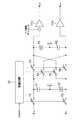
図1に、本実施形態にかかるチョッパ型信号サンプル回路を示す。 FIG. 1 shows a chopper type signal sample circuit according to the present embodiment.
本実施例のチョッパ型信号サンプル回路は、サンプル時間に比べホールド時間が長いサンプルシステムにおいて、極性の変換をホールド動作時に行うことを特徴とする。スイッチのチョッパ動作をサンプル動作時に行うのではなく、ホールド動作時に行う。具体的に、アナログ入力信号をサンプルする容量に対し、当該容量の入力側ではなく、出力側(アンプ側)にチョッパ動作のためのスイッチを設ける。これにより、チョッパ用に小さなサイズのスイッチを用いることができ、回路を小面積化できる。以下、本実施例について、さらに詳細に説明する。 The chopper type signal sampling circuit of the present embodiment is characterized in that polarity conversion is performed during a hold operation in a sample system having a hold time longer than the sample time. The switch chopper operation is not performed during the sample operation, but is performed during the hold operation. Specifically, a switch for chopper operation is provided on the output side (amplifier side) of the capacitor for sampling the analog input signal, not on the input side of the capacitor. Thereby, a small-sized switch can be used for the chopper, and the circuit area can be reduced. Hereinafter, the present embodiment will be described in more detail.
図1に示すチョッパ型信号サンプル回路は、第1および第2のサンプルスイッチとしてのサンプルスイッチT1,T2と、第1および第2のサンプル容量としての2つのサンプル容量C1,C2と、第1〜第4のチョッパスイッチとしてのチョッパスイッチT3,T4,T5,T6と、アンプ11と、制御回路12を備える。P1、P2は、アンプの入力側に存在する寄生容量を表す。 The chopper type signal sample circuit shown in FIG. 1 includes sample switches T1, T2 as first and second sample switches, two sample capacitors C1, C2 as first and second sample capacitors, Chopper switches T3, T4, T5, and T6 as a fourth chopper switch, an
サンプルスイッチT1の一端には正側アナログ入力信号、サンプルスイッチT2の一端には負側アナログ入力信号が入力される。正側アナログ入力信号および負側入力アナログ信号は、差動信号を構成する。 A positive analog input signal is input to one end of the sample switch T1, and a negative analog input signal is input to one end of the sample switch T2. The positive side analog input signal and the negative side input analog signal constitute a differential signal.
サンプルスイッチT1の他端には、サンプル容量C1の一端が接続されている。サンプル容量C1の他端はグランドに接続されている。グランドはAC的なグランドであればよく、実際は任意の固定電圧でもかまわない。サンプルスイッチT2の他端には、サンプル容量C2の一端が接続されている。サンプル容量C2の他端はグランドに接続されている。 One end of a sample capacitor C1 is connected to the other end of the sample switch T1. The other end of the sample capacitor C1 is connected to the ground. The ground may be an AC ground and may be any fixed voltage in practice. One end of a sample capacitor C2 is connected to the other end of the sample switch T2. The other end of the sample capacitor C2 is connected to the ground.
また、サンプルスイッチT1の他端は、チョッパスイッチT3,T4の入力に接続されている。サンプルスイッチT2の他端は、チョッパスイッチT5,T6の入力に接続されている。 The other end of the sample switch T1 is connected to the inputs of the chopper switches T3 and T4. The other end of the sample switch T2 is connected to the inputs of the chopper switches T5 and T6.
チョッパスイッチT3,T5の出力は互いに接続されるとともに、アンプの正側入力端子に接続されている。チョッパスイッチT4,T6の出力は互いに接続されるとともに、アンプ11の負側入力端子に接続されている。 The outputs of the chopper switches T3 and T5 are connected to each other and to the positive input terminal of the amplifier. The outputs of the chopper switches T4 and T6 are connected to each other and to the negative input terminal of the
制御回路12は、外部から入力されるクロックにしたがって動作する。制御回路12は、サンプルスイッチT1,T2を同じオンオフ状態に切り替え制御する。すなわち、サンプル周期毎に、サンプルスイッチT1,T2を同時にオンにするサンプルスイッチ制御信号を生成する。サンプルスイッチT1,T2をオンにするサンプルスイッチ制御信号は、たとえばハイレベル(“1”)を有する。サンプルスイッチT1,T2は、このオンのサンプルスイッチ制御信号に応じて駆動され、それぞれオンにされる。 The
制御回路12は、サンプル動作期間経過後、サンプルスイッチT1,T2を同時にオフにするサンプルスイッチ制御信号を生成する。サンプルスイッチT1,T2をオフにするサンプルスイッチ制御信号は、たとえばローレベル(“0”)を有する。サンプルスイッチT1,T2は、このオフのサンプルスイッチ制御信号に応じて駆動される、それぞれオフになる。サンプルスイッチ制御信号がハイレベル(“1”)の期間はサンプル期間、“0”の期間はホールド期間に対応する。 The
また制御回路12は、周期的または所定のタイミングで、チョッパスイッチT3,T6を同じオンオフ状態に切り替え制御し、チョッパスイッチT4,T5を同じオンオフ状態に切り替え制御する。この際、チョッパスイッチT3,T6をチョッパスイッチT4,T5と相補動作させる。すなわち、どちらか一方の組がオンのとき、他方の組はオフである。 Further, the
より詳細には、制御回路12は、ランダム信号発生器を備え、これを用いて、チョッパスイッチT3,T6を制御する第1チョッパスイッチ制御信号と、チョッパスイッチT4,T5を制御する第2チョッパスイッチ制御信号との2つのチョッパスイッチ制御信号を生成する。 More specifically, the
これら2つのチョッパスイッチ制御信号は相補の関係にある。第1チョッパスイッチ制御信号がオン(“1”)を示すとき、第2チョッパスイッチ制御信号はオフ(“0”)を示す。第1チョッパスイッチ制御信号がオフを示すとき、第2チョッパスイッチ制御信号はオンを示す。 These two chopper switch control signals are in a complementary relationship. When the first chopper switch control signal indicates ON (“1”), the second chopper switch control signal indicates OFF (“0”). When the first chopper switch control signal indicates OFF, the second chopper switch control signal indicates ON.
これらチョッパスイッチ制御信号の極性は、周期的または所定のタイミングで、ランダムに変化させる。サンプルスイッチ制御信号がオンのタイミングで変化する構成(図3参照)、またはサンプルスイッチ制御信号がオフになるタイミングで変化する構成が可能である。または、サンプルスイッチ制御信号がオンになったタイミングから一定時間後(サンプルスイッチ制御信号がオフになるタイミング以前)でもよい。 The polarities of these chopper switch control signals are changed randomly or periodically or at a predetermined timing. A configuration in which the sample switch control signal changes at the on timing (see FIG. 3) or a configuration in which the sample switch control signal changes at the off timing is possible. Alternatively, it may be after a certain time from the timing when the sample switch control signal is turned on (before the timing when the sample switch control signal is turned off).
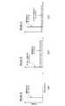
図3に、図1に示す回路のタイミングチャートを示す。 FIG. 3 shows a timing chart of the circuit shown in FIG.
図3(A)はアナログ入力信号Ain、図3(B)は出力信号Aout、図3(C)はサンプルスイッチT1,T2用制御信号(サンプルスイッチ制御信号)、図3(D)はチョッパスイッチT3,T6用制御信号(第1チョッパスイッチ制御信号)、図3(E)はチョッパスイッチT4,T5用制御信号(第2チョッパスイッチ制御信号)を示す。アナログ入力信号Ainは、図1のAin+とAin-との差分(Ain=Ain+-Ain-)を意味する。出力信号Aoutは、Aout+とAout-との差分を意味する。3A is an analog input signal Ain , FIG. 3B is an output signal Aout , FIG. 3C is a control signal for the sample switches T1 and T2 (sample switch control signal), and FIG. A control signal for the chopper switches T3 and T6 (first chopper switch control signal) and FIG. 3E shows a control signal for the chopper switches T4 and T5 (second chopper switch control signal). The analog input signal Ain means the difference between Ain + and Ain−in FIG. 1 (Ain = Ain + −Ain− ). The output signal Aout means a difference between Aout + and Aout− .
上述のように、この回路でのサンプルは、サンプルスイッチ制御信号が1の期間、行われる。サンプルスイッチ制御信号が0の期間は、すべてホールド期間である。 As described above, sampling in this circuit is performed while the sample switch control signal is 1. All periods when the sample switch control signal is 0 are hold periods.
第1チョッパスイッチ制御信号と第2チョッパスイッチ制御信号は、上述のように互いに異なる極性で生成され、それぞれの極性はランダムに決定される。本例では、第1チョッパスイッチ制御信号と第2チョッパスイッチ制御信号は、サンプルスイッチ制御信号の正側エッジ(立ち上がりエッジ)に同期して生成される。第1チョッパスイッチ制御信号と第2チョッパスイッチ制御信号は相補の関係にあるため、同時に1となることは無く、また同時に0となることも無い。 The first chopper switch control signal and the second chopper switch control signal are generated with different polarities as described above, and the respective polarities are randomly determined. In this example, the first chopper switch control signal and the second chopper switch control signal are generated in synchronization with the positive edge (rising edge) of the sample switch control signal. Since the first chopper switch control signal and the second chopper switch control signal are in a complementary relationship, they are not 1 at the same time and are not 0 at the same time.
サンプルスイッチ制御信号は、第1または第2チョッパスイッチ制御信号と同時に1となる期間をもつ。これは、寄生容量P1,P2(図1参照)の影響を緩和するためである。たとえば、サンプルスイッチ制御信号と、第1または第2チョッパスイッチ制御信号を同時に1としない (non-overlap clock)場合、サンプル期間ではサンプルスイッチ制御信号のみがオン状態となり、サンプル容量C1,C2のみに、信号のサンプルが行われる。ホールド期間では、サンプルスイッチ制御信号がオフ状態、第1または第2チョッパスイッチ制御信号がオン状態となり、サンプル容量C1,C2と、寄生容量P1,P2が並列接続されることになる。これにより、サンプル容量C1,C2と寄生容量P1,P2との間で、サンプル容量C1,C2に蓄積された信号電荷の再分配が起こり、不要な信号電荷が加算あるいは減算される。これにより、歪が発生する。 The sample switch control signal has a period of 1 simultaneously with the first or second chopper switch control signal. This is to mitigate the influence of the parasitic capacitances P1 and P2 (see FIG. 1). For example, if the sample switch control signal and the first or second chopper switch control signal are not simultaneously set to 1 (non-overlap clock), only the sample switch control signal is on during the sample period, and only the sample capacities C1 and C2 The signal is sampled. In the hold period, the sample switch control signal is turned off, the first or second chopper switch control signal is turned on, and the sample capacitors C1 and C2 and the parasitic capacitors P1 and P2 are connected in parallel. Thereby, redistribution of signal charges accumulated in the sample capacitors C1 and C2 occurs between the sample capacitors C1 and C2 and the parasitic capacitors P1 and P2, and unnecessary signal charges are added or subtracted. Thereby, distortion occurs.
これに対し、本回路では、サンプル動作の際、サンプルスイッチ制御信号と、第1または第2チョッパスイッチ制御信号とを同時にオン状態とする期間をもつため、サンプル容量C1,C2だけでなく、寄生容量P1,P2に対しても信号のサンプルが行われる。このため、電荷の再配分の問題は発生しないか、もしくは低減される。一般的に、寄生容量P1,P2はサンプル容量C1,C2に対し十分小さいため、チョッパスイッチのオン抵抗値に対する要求が緩和される。またサンプル時間に比べ長いホールド時間にチョッパ動作を行っており、これにより、チョッパのための動作期間を長くすることができる。これらのため、極性変換に用いられるチョッパスイッチT3,T4,T5,T6として、小さいサイズのものを用いることができる。 In contrast, this circuit has a period during which the sample switch control signal and the first or second chopper switch control signal are turned on at the same time during the sample operation. Signal sampling is also performed on the capacitors P1 and P2. Thus, the problem of charge redistribution does not occur or is reduced. In general, since the parasitic capacitances P1 and P2 are sufficiently smaller than the sample capacitances C1 and C2, the requirement for the on-resistance value of the chopper switch is eased. In addition, the chopper operation is performed in the hold time longer than the sample time, and thus the operation period for the chopper can be lengthened. For these reasons, small chopper switches T3, T4, T5, and T6 used for polarity conversion can be used.
サンプルスイッチ制御信号が“1”の間、サンプル容量C1,C2に電荷が蓄積され、“0”の間、これらの電荷が保持される(信号ホールド)。この電荷は、次のサンプルスイッチ制御信号が1となるまで、容量C1,C2に保持され続ける。サンプル容量に蓄積された電荷(あるいは電圧)は、通常、チョッパ型サンプル回路の外部の負荷(図示せず)を駆動する。アンプ11は、保持された電圧のための駆動回路として用いられる。アンプ11の増幅利得は後段の回路に応じて決定すればよい。たとえば1倍とすることが考えられる。 While the sample switch control signal is “1”, charges are accumulated in the sample capacitors C1 and C2, and during “0”, these charges are held (signal hold). This charge continues to be held in the capacitors C1 and C2 until the next sample switch control signal becomes 1. The electric charge (or voltage) accumulated in the sample capacitor usually drives a load (not shown) outside the chopper type sample circuit. The
ここで、正側のサンプル容量C1に蓄積された電荷は、チョッパスイッチT3がオンで、チョッパスイッチT4がオフのときは、アンプ11の正側入力端子に入力され、チョッパスイッチT3がオフで、チョッパスイッチT4がオンのときは、アンプ11の負側入力端子に入力される。同様に、負側のサンプル容量C2に蓄積された電荷は、チョッパスイッチT6がオンで、チョッパスイッチT5がオフのときは、アンプ11の負側入力端子に、チョッパスイッチT6がオフで、チョッパスイッチT5がオンのときは、アンプ11の正側入力端子に入力される。このように、ランダムに極性が変化する第1および第2チョッパスイッチ制御信号次第で、各サンプル容量からアンプ11への入力極性が変わる(チョッパ動作)。アンプ11は、正側入力端子に入力された信号を増幅し、増幅正側信号を正側出力端子から出力する。またアンプ11は、負側入力端子に入力された信号を増幅し、増幅正側信号を負側出力端子から出力する。 Here, when the chopper switch T3 is on and the chopper switch T4 is off, the charge accumulated in the positive side sample capacitor C1 is input to the positive side input terminal of the
なお、図3の例では、サンプルスイッチ制御信号と第1または第2チョッパスイッチ制御信号の立ち上がりエッジは一致しているが、サンプル動作期間でサンプルスイッチ制御信号と、第1または第2チョッパスイッチ制御信号とが同時にオン状態となる期間をもつ限り、必ずしも一致する必要は無い。第1または第2チョッパスイッチ制御信号が、サンプルスイッチ制御信号のオン期間を完全にカバーしていなくても良い。なお、サンプル動作期間でサンプルスイッチ制御信号と、第1または第2チョッパスイッチ制御信号とが同時にオン状態となる期間をもつことは本実施例の必須要件ではなく、この場合も後述する本実施例の効果(低回路面積効果)を享受可能である。 In the example of FIG. 3, the rising edge of the sample switch control signal and the first or second chopper switch control signal match, but the sample switch control signal and the first or second chopper switch control are in the sample operation period. As long as there is a period in which the signals are in the ON state at the same time, they do not necessarily coincide. The first or second chopper switch control signal may not completely cover the ON period of the sample switch control signal. Note that it is not an essential requirement of the present embodiment that the sample switch control signal and the first or second chopper switch control signal are simultaneously turned on in the sample operation period, and this embodiment will be described later in this case as well. (Effect of low circuit area) can be enjoyed.
寄生容量P1,P2への信号サンプルの時間は、チョッパスイッチT3,T4,T5,T6のオン抵抗と寄生容量値とで求まる時定数により決定される。このため、サンプルスイッチ制御信号の立ち下がりエッジは、第1または第2チョッパスイッチ制御信号のオン期間に重なっている必要があり、かつ、その重なり時間もその時定数と同等あるいはそれ以上が必要である。 The time of signal sampling to the parasitic capacitances P1 and P2 is determined by a time constant determined by the on resistance of the chopper switches T3, T4, T5, and T6 and the parasitic capacitance value. For this reason, the falling edge of the sample switch control signal must overlap the ON period of the first or second chopper switch control signal, and the overlap time must be equal to or more than the time constant. .
上記のようにして入力アナログ信号がチョッパスイッチT3,T4,T5,T6によりチョッパされることで、当該信号はスペクトラム拡散される。アンプ11には、スペクトラム拡散された信号が入力される。アンプ11の後段には、復調回路(図4参照)を設けて、当該復調回路で、スペクトラム拡散された信号を復調する。復調された信号をAD変換することでデジタルコードを得ることができる。 When the input analog signal is choppered by the chopper switches T3, T4, T5, and T6 as described above, the signal is spread spectrum. The
図4に、図1に示すチョッパ型信号サンプル回路の後段に復調回路を設けた構成を示す。 FIG. 4 shows a configuration in which a demodulation circuit is provided in the subsequent stage of the chopper type signal sample circuit shown in FIG.
図4では、復調回路をアナログ回路で実現する構成が示されている。この復調回路は、第5〜第8チョッパスイッチとしての4つのスイッチT7,T8,T9,T10を備える。スイッチT7,T10には、チョッパスイッチT3,T6と同じ第1チョッパスイッチ制御信号が入力される。スイッチT8,T9には、チョッパスイッチT4,T5と同じ第2チョッパスイッチ制御信号が入力される。このようにスイッチT7、T8、T9、T10が制御されることで、チョッパ動作によりアンプ11の入力側で信号の極性が変換された場合は、復調回路側でも極性を変換する。また、チョッパ動作でアンプ11の入力側で信号の極性が変換されなかった場合は、復調回路側でも極性を変換しない。復調回路の後段にAD変換器を配置し、復調された信号をAD変換することで、デジタルコードを得ることができる。 FIG. 4 shows a configuration in which the demodulation circuit is realized by an analog circuit. The demodulating circuit includes four switches T7, T8, T9, and T10 as fifth to eighth chopper switches. The same first chopper switch control signal as the chopper switches T3 and T6 is input to the switches T7 and T10. The same second chopper switch control signal as the chopper switches T4 and T5 is input to the switches T8 and T9. By controlling the switches T7, T8, T9, and T10 in this way, when the polarity of the signal is converted on the input side of the
図5に、図4の入力ノードA、アンプ出力ノードB、出力ノードCにおける信号のスペクトラムの一例を示す。図5(A)が入力ノードA、図5(B)がアンプ出力ノードB、図4(C)が出力ノードCの信号スペクトラムを表す。 FIG. 5 shows an example of the spectrum of signals at input node A, amplifier output node B, and output node C in FIG. 5A shows the signal spectrum of the input node A, FIG. 5B shows the signal spectrum of the amplifier output node B, and FIG. 4C shows the signal spectrum of the output node C.
図5(A)に示すように、入力信号として単一正弦波が入力されていることを仮定している。 As shown in FIG. 5 (A), it is assumed that a single sine wave is input as an input signal.
図5(B)に示すように、アンプ出力ノードBでは、チョッパスイッチT3〜T6によるチョッパ動作により、入力信号がスペクトラム拡散されることで、周波数全域に均一に入力信号成分が広がる。この信号帯域に、アンプ11の入力に存在する入力換算オフセットのスペクトル(DC直流成分)が重畳される。アンプ11の入力に存在する入力換算オフセットを模式的に図2に示す。アンプ11はアンプ11a、12bを含み、ここではアンプ11aの入力換算オフセットが示される。アンプ12bにも実際には入力換算オフセットが存在する。アンプ11aの入力は、チョッパスイッチT3,T5の出力に接続され、アンプ12bの入力は、チョッパスイッチT4,T6の出力に接続されている。 As shown in FIG. 5 (B), at the amplifier output node B, the input signal component spreads uniformly over the entire frequency range by the spectrum spread of the input signal by the chopper operation by the chopper switches T3 to T6. The spectrum of the input conversion offset (DC direct current component) existing at the input of the
図5(C)に示すように、出力ノードCでは、チョッパスイッチT7〜T10によるチョッパ動作により、スペクトラム拡散された入力信号が復元され、元の単一正弦波に戻る。一方、アンプ11で加算された入力換算オフセット(図5(B)参照)が、チョッパスイッチT7〜T10のチョッパ動作によりスペクトラム拡散されるため、周波数全域に均一にオフセット成分が広がる。オフセット成分(DC成分)がスペクトラム拡散されることで、オペアンプ11が本来有するDC成分(図5(B))よりも、オフセットが低減できている様子がわかる。 As shown in FIG. 5 (C), at the output node C, the spread spectrum input signal is restored by the chopper operation by the chopper switches T7 to T10, and returns to the original single sine wave. On the other hand, since the input conversion offset (see FIG. 5B) added by the
図6に、チョッパ型信号サンプル回路の後段の復調回路をデジタル回路で構成した例を示す。 FIG. 6 shows an example in which the demodulator circuit in the subsequent stage of the chopper type signal sample circuit is configured with a digital circuit.
基本となるアナログ部分の回路は、図1の回路と同様であるが、AD変換器(A/D converter)13と、デジタル乗算回路(極性変換回路)14が追加されている。 The basic analog circuit is the same as the circuit of FIG. 1, except that an AD converter (A / D converter) 13 and a digital multiplier circuit (polarity conversion circuit) 14 are added.
AD変換器13は、アンプ11の出力信号をAD変換して、デジタル信号(デジタルコード)を生成する。デジタル乗算回路14では、デジタル信号に、1あるいは-1の信号を乗算することで、出力信号の極性を制御する。たとえば、チョッパスイッチT3、T6がオン(“1”)の場合にAD変換器13から出力されたデジタルコードに1の信号を乗算する。チョッパスイッチT4,T5がオンの場合にAD変換器13から出力されたデジタル信号には-1の信号を乗算する。これにより、極性を変換する。 The
このように、スイッチT3〜T6のチョッパ動作によりスペクトラム拡散された入力信号を、デジタル乗算回路14によりデジタル領域で復調している。これによれば、復調回路を簡単化できる。また、アンプ11とAD変換器13が有するオフセット成分を低減できる効果を有する。 In this way, the input signal that has been subjected to spectrum spread by the chopper operation of the switches T3 to T6 is demodulated in the digital domain by the
以上のように図6の構成により、チョッパ復調のための回路を小型化することができる。また、アンプからAD変換器までのオフセットをスペクトラム拡散できる。 As described above, the circuit for chopper demodulation can be reduced in size by the configuration of FIG. Also, the spread from the amplifier to the AD converter can be spread spectrum.
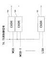
図7に、デジタル乗算回路の具体例を示す。 FIG. 7 shows a specific example of the digital multiplication circuit.
デジタル領域での極性反転操作は、方式にもよるが、たとえば各ビットを反転することで実現できる。1回のサンプル動作およびAD変換で得られたビット列(MSB、MSB-1、MSB-2、・・・LSB)における各ビットを、T4,T5用制御信号に応じて反転させる。具体的に、T4,T5用制御信号が0のとき、各ビットを反転させず、T4,T5用制御信号が1のとき、各ビットを反転させる。この操作は、各ビットに対応配置された排他的論理和回路(EXOR回路)16A,16B…,16Cにより実現できる。各排他的論理和回路の一方の入力は、ビット列における対応ビット、他方の入力はT4,T5用制御信号である。T4,T5用制御信号が1のとき、入力ビットが1であれば出力は0、入力ビットが0であれば出力は1であり、ビットが反転される。T4,T5用制御信号が0のとき、入力ビットが0であれば出力は0、入力ビットが1であれば出力は1であり、ビットは反転されない。 The polarity inversion operation in the digital domain can be realized by inverting each bit, for example, depending on the method. Each bit in the bit string (MSB, MSB-1, MSB-2,... LSB) obtained by one sampling operation and AD conversion is inverted according to the control signal for T4 and T5. Specifically, when the control signal for T4 and T5 is 0, each bit is not inverted, and when the control signal for T4 and T5 is 1, each bit is inverted. This operation can be realized by exclusive OR circuits (EXOR circuits) 16A, 16B,..., 16C arranged corresponding to each bit. One input of each exclusive OR circuit is a corresponding bit in the bit string, and the other input is a control signal for T4 and T5. When the control signal for T4 and T5 is 1, if the input bit is 1, the output is 0, and if the input bit is 0, the output is 1 and the bit is inverted. When the control signal for T4 and T5 is 0, if the input bit is 0, the output is 0, and if the input bit is 1, the output is 1 and the bit is not inverted.
なお、ここではAD変換器の変換に要する遅延(レイテンシ)が0であることを仮定している。実際には、AD変換器にはレイテンシが存在するため、T4,T5用の制御信号を遅延させて、入力する。これにより、AD変換器の出力コードのMSBと、T4,T5用の制御信号とが同期して、排他的論理和回路に入力されるようにする。遅延量は、AD変換器のレイテンシに合わせて制御回路12内で調整する。なお、AD変換器の遅延が存在しない場合は、制御信号を遅延させる必要はない。 Here, it is assumed that the delay (latency) required for conversion by the AD converter is zero. Actually, since there is latency in the AD converter, the control signals for T4 and T5 are delayed and input. As a result, the MSB of the output code of the AD converter and the control signals for T4 and T5 are synchronized and input to the exclusive OR circuit. The delay amount is adjusted in the
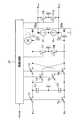
図8に、第2実施形態にかかるチョッパ型信号サンプル回路を示す。 FIG. 8 shows a chopper type signal sample circuit according to the second embodiment.
基本となる回路は、図1の回路と同様であるが、新たに、第1〜第4リセットスイッチとしてのリセットスイッチT7,T8,T9,T10が追加されている点が異なる。 The basic circuit is the same as the circuit of FIG. 1, except that reset switches T7, T8, T9, and T10 as first to fourth reset switches are newly added.
本回路は、アンプ32の入出力間に存在する寄生容量の影響を緩和することである。アンプ入出力間に寄生容量が存在すると、サンプル動作の際、サンプル動作直前まで寄生容量に保持されていた電圧の影響を受けるため(メモリー効果)、歪特性が劣化する。この問題を解決するため、本回路ではリセットスイッチを設けている。サンプル動作前にアンプ32の入力と出力をそれぞれグランドへリセットすることで、メモリー効果の影響を緩和することができる。 This circuit is to alleviate the influence of parasitic capacitance existing between the input and output of the
本構成では、図1に示した構成と異なり、アンプの入力側のみならず、出力側に寄生する容量も考慮している。アンプの出力電圧が高速に入力電圧に追従する能力が無いことを想定している。アンプ出力電圧が入力電圧に0時間で追従できない場合、入力と出力との間で電位差が生じ、これにより不要な電荷が、寄生容量に蓄積される。この不要電荷は入力信号のサンプル容量に注入されることになる。入力信号が直流であれば、理想的には電位差は常に0となるため、この問題は発生しないが、時間的に変化する入力信号をサンプルする場合、サンプル毎に異なる電位差が生じるため、毎回異なる電荷が、サンプル容量に注入される。これが、歪特性劣化の原因となる(履歴効果)。本構成では、この履歴効果の影響をキャンセルするため、アンプ入出力にそれぞれリセットスイッチを設けている。 Unlike the configuration shown in FIG. 1, this configuration takes into account not only the input side of the amplifier but also the parasitic capacitance on the output side. It is assumed that the output voltage of the amplifier is not capable of following the input voltage at high speed. When the amplifier output voltage cannot follow the input voltage in 0 hours, a potential difference is generated between the input and the output, and unnecessary charges are accumulated in the parasitic capacitance. This unnecessary charge is injected into the sample capacity of the input signal. If the input signal is a direct current, the potential difference is ideally always 0, so this problem does not occur. However, when an input signal that changes over time is sampled, a different potential difference is generated for each sample, so it differs every time. Charge is injected into the sample volume. This causes distortion characteristic deterioration (history effect). In this configuration, in order to cancel the influence of the history effect, a reset switch is provided for each of the amplifier inputs and outputs.
図9に、図8の回路の具体例を示す。 FIG. 9 shows a specific example of the circuit of FIG.
アンプ32が、2つの単相ソースフォロアアンプ32a,32bにより実現されている。この回路の場合、ソースフォロアアンプ32aの入力トランジスタM1のゲート・ソース間、およびソースフォロアアンプ32bの入力トランジスタM2のゲート・ソース間に寄生容量が存在する。 The
サンプル動作が行われている最中、ノードXにはアナログ入力信号と同じ電圧が印加されるが、アンプの出力は、アナログ入力と同じ大きさの電圧が印加されることは無い。これは、アンプの駆動能力が有限であるためである。 While the sample operation is being performed, the same voltage as the analog input signal is applied to the node X, but the voltage of the same magnitude as that of the analog input is not applied to the output of the amplifier. This is because the drive capability of the amplifier is finite.
サンプル動作最中に、アンプの出力が変動しているため、入力信号とアンプ出力信号との差分電圧に相当する電荷が寄生容量に蓄積される。アンプ出力の変動は、サンプル終了以降も継続されるため、サンプル終了以降の変動電圧に相当する電荷がサンプル容量C1、C2に加わることになる。これにより誤差信号が発生する。この誤差は、アンプ出力の変動の大きさに応じて変化するため、結果的に歪性能劣化の原因となる。 Since the output of the amplifier fluctuates during the sampling operation, the charge corresponding to the differential voltage between the input signal and the amplifier output signal is accumulated in the parasitic capacitance. Since the fluctuation of the amplifier output continues after the end of the sample, the charge corresponding to the fluctuation voltage after the end of the sample is added to the sample capacitors C1 and C2. As a result, an error signal is generated. Since this error changes according to the magnitude of the fluctuation of the amplifier output, as a result, it causes distortion performance deterioration.
図10に、本回路のタイミングチャートを示す。サンプルスイッチT1,T2用のサンプル制御信号がオン(“1”)になる前に、リセットスイッチT7,T8,T9,T10用制御信号をオン(“1”)にする。これによりアンプの入力ノードとアンプの出力ノードが一端リセットされ、グランド(電圧“0”)にセットされる。つまり、入力トランジスタのゲートとソースの電位差が0にされる。その後、サンプル動作が開始される。このようにして、サンプル開始前に、寄生容量に記憶されていた電荷の履歴はキャンセルされ、よって歪特性劣化を低減できる。 FIG. 10 shows a timing chart of this circuit. Before the sample control signals for the sample switches T1 and T2 are turned on (“1”), the control signals for the reset switches T7, T8, T9, and T10 are turned on (“1”). As a result, the amplifier input node and the amplifier output node are reset once and set to the ground (voltage “0”). That is, the potential difference between the gate and source of the input transistor is set to zero. Thereafter, the sample operation is started. In this way, the charge history stored in the parasitic capacitance before the start of sampling is canceled, so that distortion characteristic deterioration can be reduced.
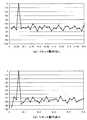
図11に、リセット動作による歪改善効果の一例を示す。図中上段がリセット動作を行わなかった場合、下段はリセット動作を行った場合である。縦軸は、出力Aout+のパワーを示し、横軸は周波数を示す。回路の動作周波数をFSとすると、横軸の値×FSが、横軸が示す周波数である。リセット動作を行った場合のSFDR(Spurious-Free Dynamic Range)は52.37、リセット動作を行わなかった場合のSFDRは、67.22であった。したがって、この例では、リセット動作により、高調波を15DB程度改善できる、すなわち歪みを小さくできる。FIG. 11 shows an example of the distortion improvement effect by the reset operation. In the figure, when the upper stage does not perform the reset operation, the lower stage is when the reset operation is performed. The vertical axis indicates the power of the output Aout + , and the horizontal axis indicates the frequency. Assuming that the operating frequency of the circuit is FS, the value xFS on the horizontal axis is the frequency indicated on the horizontal axis. The SFDR (Spurious-Free Dynamic Range) when the reset operation was performed was 52.37, and the SFDR when the reset operation was not performed was 67.22. Therefore, in this example, the reset operation can improve the harmonics by about 15 DB, that is, the distortion can be reduced.
図12は、図10の回路の後段に、デジタル復調回路を配置した回路を示す。 FIG. 12 shows a circuit in which a digital demodulation circuit is arranged after the circuit of FIG.
デジタル復調回路は、AD変換器13とデジタル乗算器14を含む。デジタル復調回路の構成および動作は、図6と同様であるため、説明を省略する。 The digital demodulation circuit includes an
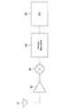
図13は、本発明の実施形態にかかる無線受信機を示す。 FIG. 13 shows a wireless receiver according to an embodiment of the present invention.
この無線受信機は、アンテナ41、LNA42、ミキサ43、アナログベースバンド回路44、AD変換回路45を備える。AD変換回路45は、これまで述べてきたチョッパ型信号サンプル回路およびAD変換器を含む。AD変換回路45は、逐次比較型AD変換回路(SAR ADC)でもよい。 This radio receiver includes an
アンテナ41で受信した無線信号をLNA(Low Noise Amplifier)42で増幅する。LNA42で増幅された無線周波数の信号を、ミキサ43でベースバンド信号にダウンコンバートし、アナログベースバンド回路44でベースバンド信号にフィルタリング処理を行って所望帯域の信号を取り出す。そして、AD変換回路45で、フィルタイリング後のアナログ信号をデジタル信号に変換する。 A radio signal received by the
なお、本発明は上記実施形態そのままに限定されるものではなく、実施段階ではその要旨を逸脱しない範囲で構成要素を変形して具体化できる。また、上記実施形態に開示されている複数の構成要素の適宜な組み合わせにより、種々の発明を形成できる。例えば、実施形態に示される全構成要素から幾つかの構成要素を削除してもよい。さらに、異なる実施形態にわたる構成要素を適宜組み合わせてもよい。 Note that the present invention is not limited to the above-described embodiment as it is, and can be embodied by modifying the constituent elements without departing from the scope of the invention in the implementation stage. In addition, various inventions can be formed by appropriately combining a plurality of components disclosed in the embodiment. For example, some components may be deleted from all the components shown in the embodiment. Furthermore, constituent elements over different embodiments may be appropriately combined.
Claims (7)
Translated fromJapanese負側アナログ信号を一端で受ける第2サンプルスイッチと、
前記第1サンプルスイッチの他端に一端が接続され、他端が固定電圧に接続された第1サンプル容量と、
前記第2サンプルスイッチの他端に一端が接続され、他端が前記固定電圧に接続された第2サンプル容量と、
正側入力端子と負側入力端子とを有し、前記正側入力端子に入力された信号を増幅して正側増幅信号を出力し、前記負側入力端子に入力された信号を増幅して負側増幅信号を出力するアンプと、
一端が前記第1サンプル容量の一端に接続され、他端が前記正側入力端子に接続された第1チョッパスイッチと、
一端が前記第1サンプル容量の一端に接続され、他端が前記負側入力端子に接続された第2チョッパスイッチと、
一端が前記第2サンプル容量の一端に接続され、他端が前記正側入力端子に接続された第3チョッパスイッチと、
一端が前記第2サンプル容量の一端に接続され、他端が前記負側入力端子に接続された第4チョッパスイッチと、
を備えた信号サンプル回路。A first sample switch for receiving a positive analog signal at one end;
A second sample switch that receives the negative analog signal at one end;
A first sample capacitor having one end connected to the other end of the first sample switch and the other end connected to a fixed voltage;
One end connected to the other end of the second sample switch, the other end of the second sample capacitor connected to the fixed voltage;
It has a positive input terminal and a negative input terminal, amplifies the signal input to the positive input terminal and outputs a positive amplified signal, amplifies the signal input to the negative input terminal An amplifier that outputs a negative amplification signal;
A first chopper switch having one end connected to one end of the first sample capacitor and the other end connected to the positive input terminal;
A second chopper switch having one end connected to one end of the first sample capacitor and the other end connected to the negative input terminal;
A third chopper switch having one end connected to one end of the second sample capacitor and the other end connected to the positive input terminal;
A fourth chopper switch having one end connected to one end of the second sample capacitor and the other end connected to the negative input terminal;
A signal sampling circuit with.
前記第1および第4チョッパスイッチは、同じオンオフ状態に切り替え制御され、
前記第2および第3チョッパスイッチは、同じオンオフ状態に切り替え制御され、
前記第1および第4チョッパスイッチは、前記第2および第3チョッパスイッチと相補的に動作し、
前記第1および第2サンプルスイッチがオンの期間のすべてまたは一部は、前記第1および第4チョッパスイッチがオンの期間、または、前記第2および第3チョッパスイッチがオンの期間と重複する
請求項1に記載の信号サンプル回路。The first and second sample switches are controlled to be switched to the same on / off state,
The first and fourth chopper switches are controlled to be switched to the same on / off state,
The second and third chopper switches are controlled to be switched to the same on / off state,
The first and fourth chopper switches operate complementarily with the second and third chopper switches,
All or part of the period in which the first and second sample switches are on overlaps with the period in which the first and fourth chopper switches are on, or the period in which the second and third chopper switches are on. Item 1. The signal sampling circuit according to Item 1.
一端が前記第1正側出力端子に接続された第5チョッパスイッチと、
一端が前記第1負側出力端子に接続された第6チョッパスイッチと、
一端が前記第1正側出力端子に接続された第7チョッパスイッチと、
一端が前記第1負側出力端子に接続された第8チョッパスイッチと、
前記第5チョッパスイッチの他端および第7チョッパスイッチの他端に接続された第2正側出力端子と、
前記第6チョッパスイッチおよび前記第8チョッパスイッチの他端に接続された第2負側出力端子と、
を備えた請求項1または2に記載の信号サンプル回路。The amplifier includes a first positive output terminal that outputs the positive amplification signal, and a first negative output terminal that outputs the negative amplification signal,
A fifth chopper switch having one end connected to the first positive output terminal;
A sixth chopper switch having one end connected to the first negative output terminal;
A seventh chopper switch having one end connected to the first positive output terminal;
An eighth chopper switch having one end connected to the first negative output terminal;
A second positive output terminal connected to the other end of the fifth chopper switch and the other end of the seventh chopper switch;
A second negative output terminal connected to the other end of the sixth chopper switch and the eighth chopper switch;
The signal sample circuit according to claim 1 or 2, further comprising:
一端が前記第1正側入力端子に接続され、他端が前記固定電圧に接続された第1リセットスイッチと、
一端が前記第1負側入力端子に接続され、他端が前記固定電圧に接続された第2リセットスイッチと、
一端が前記第1正側出力端子に接続され、他端が前記固定電圧に接続された第3リセットスイッチと、
一端が前記第1負側出力端子に接続され、他端が前記固定電圧に接続された第4リセットスイッチと
前記第1および第2サンプルスイッチをオンにする前に、前記第1〜第4のリセットスイッチをオンにするように制御する制御回路と、
をさらに備えた請求項信号サンプル回路。The amplifier includes a first positive output terminal that outputs the positive amplification signal, and a first negative output terminal that outputs the negative amplification signal,
A first reset switch having one end connected to the first positive input terminal and the other end connected to the fixed voltage;
A second reset switch having one end connected to the first negative input terminal and the other end connected to the fixed voltage;
A third reset switch having one end connected to the first positive output terminal and the other end connected to the fixed voltage;
Before turning on the first reset switch and the fourth reset switch having one end connected to the first negative output terminal and the other end connected to the fixed voltage, the first to fourth A control circuit that controls to turn on the reset switch;
The signal sample circuit of claim 1 further comprising:
前記第1および第4チョッパスイッチを制御する第1制御信号、前記第2および第3チョッパスイッチを制御する第2制御信号を生成する制御回路と、
前記第1制御信号および前記第2制御信号の少なくとも一方に基づいて、前記デジタルコードの極性を制御する極性変換回路と、
をさらに備えた請求項1ないし4のいずれか一項に記載の信号サンプル回路。An AD converter that generates a digital code by performing AD conversion based on the positive side amplification signal and the negative side amplification signal;
A control circuit for generating a first control signal for controlling the first and fourth chopper switches, a second control signal for controlling the second and third chopper switches, and
A polarity conversion circuit for controlling the polarity of the digital code based on at least one of the first control signal and the second control signal;
5. The signal sampling circuit according to claim 1, further comprising:
請求項5に記載の信号サンプル回路。6. The signal sample circuit according to claim 5, wherein the polarity conversion circuit inverts the polarity of the second digital code when the first control signal indicates OFF or when the second control signal indicates ON.
前記アンテナで受信された無線信号を増幅する増幅器と、
前記増幅器で増幅された信号をベースバンド信号へ変換するミキサと、
前記ベースバンド信号をフィルタリング処理するアナログベースバンド部と、
前記フィルタリング処理された信号をサンプリングする、請求項1ないし6のいずれか一項に記載の信号サンプル回路を含むAD変換部と、
を備えた無線受信機。An antenna for receiving radio signals;
An amplifier for amplifying a radio signal received by the antenna;
A mixer for converting the signal amplified by the amplifier into a baseband signal;
An analog baseband unit for filtering the baseband signal;
The AD conversion unit including the signal sample circuit according to any one of claims 1 to 6, which samples the filtered signal;
With wireless receiver.
Priority Applications (2)
| Application Number | Priority Date | Filing Date | Title |
|---|---|---|---|
| JP2012178407AJP2014036420A (en) | 2012-08-10 | 2012-08-10 | Signal sampling circuit and radio receiver |
| US13/961,786US20140045444A1 (en) | 2012-08-10 | 2013-08-07 | Signal sampling circuit and radio receiver |
Applications Claiming Priority (1)
| Application Number | Priority Date | Filing Date | Title |
|---|---|---|---|
| JP2012178407AJP2014036420A (en) | 2012-08-10 | 2012-08-10 | Signal sampling circuit and radio receiver |
Publications (1)
| Publication Number | Publication Date |
|---|---|
| JP2014036420Atrue JP2014036420A (en) | 2014-02-24 |
Family
ID=50066551
Family Applications (1)
| Application Number | Title | Priority Date | Filing Date |
|---|---|---|---|
| JP2012178407APendingJP2014036420A (en) | 2012-08-10 | 2012-08-10 | Signal sampling circuit and radio receiver |
Country Status (2)
| Country | Link |
|---|---|
| US (1) | US20140045444A1 (en) |
| JP (1) | JP2014036420A (en) |
Cited By (2)
| Publication number | Priority date | Publication date | Assignee | Title |
|---|---|---|---|---|
| JP2017153051A (en)* | 2016-02-26 | 2017-08-31 | 旭化成エレクトロニクス株式会社 | Incremental delta-sigma modulator and incremental delta-sigma a/d converter |
| JP2017225031A (en)* | 2016-06-16 | 2017-12-21 | 国立大学法人大阪大学 | A/d converter and electronic apparatus |
Families Citing this family (7)
| Publication number | Priority date | Publication date | Assignee | Title |
|---|---|---|---|---|
| US10205462B2 (en)* | 2014-12-17 | 2019-02-12 | Analog Devices, Inc. | SAR ADCs with dedicated reference capacitor for each bit capacitor |
| US9641189B2 (en)* | 2014-12-17 | 2017-05-02 | Analog Devices, Inc. | Calibration techniques for SAR ADCs with on-chip reservoir capacitors |
| WO2016183235A1 (en)* | 2015-05-11 | 2016-11-17 | Yang Xu | Circuits for switched capacitor receiver front-ends |
| US9722746B2 (en)* | 2015-09-22 | 2017-08-01 | Mediatek Inc. | Analog-to-digital converter with bandpass noise transfer function |
| JP6673084B2 (en)* | 2016-08-01 | 2020-03-25 | 株式会社デンソー | Light flight type distance measuring device |
| CN107800435B (en)* | 2017-11-27 | 2023-08-25 | 广州安凯微电子股份有限公司 | Compensation circuit and cancellation method for parasitic effect of capacitor array |
| CN117833916B (en)* | 2024-02-29 | 2024-07-02 | 深圳市恒运昌真空技术股份有限公司 | Signal conditioning circuit, device and radio frequency power supply |
Citations (10)
| Publication number | Priority date | Publication date | Assignee | Title |
|---|---|---|---|---|
| JPS56107398A (en)* | 1980-01-17 | 1981-08-26 | Trw Inc | Differential sampleeholding circuit |
| JPH0845298A (en)* | 1994-07-29 | 1996-02-16 | Nec Corp | Differential sample-and-hold circuit |
| JPH10117219A (en)* | 1996-05-10 | 1998-05-06 | Motorola Inc | Method and circuit for attenuating base-band signal |
| JP2000504535A (en)* | 1996-11-29 | 2000-04-11 | コーニンクレッカ フィリップス エレクトロニクス エヌ ヴィ | Analog-digital conversion |
| JP2002530916A (en)* | 1998-11-12 | 2002-09-17 | コーニンクレッカ フィリップス エレクトロニクス エヌ ヴィ | Circuit having means for reducing DC offset and noise generated by an amplifier |
| JP2007243638A (en)* | 2006-03-09 | 2007-09-20 | Olympus Corp | Amplifying circuit, and high gain module using the same |
| JP2008219404A (en)* | 2007-03-02 | 2008-09-18 | Sanyo Electric Co Ltd | Amplifier circuit |
| JP2011249893A (en)* | 2010-05-24 | 2011-12-08 | A-R-Tec Corp | Delta-sigma ad converter |
| JP2012502581A (en)* | 2008-09-11 | 2012-01-26 | アナログ デバイセス インコーポレーテッド | Automatic correction feedback loop for offset and ripple suppression in chopper stabilized amplifiers |
| JP2012054766A (en)* | 2010-09-01 | 2012-03-15 | Olympus Corp | Chopper stabilized amplifier |
Family Cites Families (2)
| Publication number | Priority date | Publication date | Assignee | Title |
|---|---|---|---|---|
| US9577608B2 (en)* | 2009-08-14 | 2017-02-21 | Qualcomm Incorporated | Discrete time lowpass filter |
| US8604861B1 (en)* | 2012-06-19 | 2013-12-10 | Infineon Technologies Ag | System and method for a switched capacitor circuit |
- 2012
- 2012-08-10JPJP2012178407Apatent/JP2014036420A/enactivePending
- 2013
- 2013-08-07USUS13/961,786patent/US20140045444A1/ennot_activeAbandoned
Patent Citations (10)
| Publication number | Priority date | Publication date | Assignee | Title |
|---|---|---|---|---|
| JPS56107398A (en)* | 1980-01-17 | 1981-08-26 | Trw Inc | Differential sampleeholding circuit |
| JPH0845298A (en)* | 1994-07-29 | 1996-02-16 | Nec Corp | Differential sample-and-hold circuit |
| JPH10117219A (en)* | 1996-05-10 | 1998-05-06 | Motorola Inc | Method and circuit for attenuating base-band signal |
| JP2000504535A (en)* | 1996-11-29 | 2000-04-11 | コーニンクレッカ フィリップス エレクトロニクス エヌ ヴィ | Analog-digital conversion |
| JP2002530916A (en)* | 1998-11-12 | 2002-09-17 | コーニンクレッカ フィリップス エレクトロニクス エヌ ヴィ | Circuit having means for reducing DC offset and noise generated by an amplifier |
| JP2007243638A (en)* | 2006-03-09 | 2007-09-20 | Olympus Corp | Amplifying circuit, and high gain module using the same |
| JP2008219404A (en)* | 2007-03-02 | 2008-09-18 | Sanyo Electric Co Ltd | Amplifier circuit |
| JP2012502581A (en)* | 2008-09-11 | 2012-01-26 | アナログ デバイセス インコーポレーテッド | Automatic correction feedback loop for offset and ripple suppression in chopper stabilized amplifiers |
| JP2011249893A (en)* | 2010-05-24 | 2011-12-08 | A-R-Tec Corp | Delta-sigma ad converter |
| JP2012054766A (en)* | 2010-09-01 | 2012-03-15 | Olympus Corp | Chopper stabilized amplifier |
Cited By (2)
| Publication number | Priority date | Publication date | Assignee | Title |
|---|---|---|---|---|
| JP2017153051A (en)* | 2016-02-26 | 2017-08-31 | 旭化成エレクトロニクス株式会社 | Incremental delta-sigma modulator and incremental delta-sigma a/d converter |
| JP2017225031A (en)* | 2016-06-16 | 2017-12-21 | 国立大学法人大阪大学 | A/d converter and electronic apparatus |
Also Published As
| Publication number | Publication date |
|---|---|
| US20140045444A1 (en) | 2014-02-13 |
Similar Documents
| Publication | Publication Date | Title |
|---|---|---|
| JP2014036420A (en) | Signal sampling circuit and radio receiver | |
| US9847790B2 (en) | Hybrid analog-to-digital converter using digital slope analog-to-digital converter and related hybrid analog-to-digital conversion method thereof | |
| van der Goes et al. | A 1.5 mW 68 dB SNDR 80 Ms/s 2$\times $ Interleaved Pipelined SAR ADC in 28 nm CMOS | |
| JP5101678B2 (en) | A / D conversion circuit and receiver | |
| US10003348B2 (en) | Analog-to-digital converter with noise shaping | |
| US20070013571A1 (en) | AD converter | |
| US9483028B1 (en) | Hybrid analog-to-digital converter | |
| Lee et al. | A CMOS 15-bit 125-MS/s time-interleaved ADC with digital background calibration | |
| Wang et al. | An event-driven quasi-level-crossing delta modulator based on residue quantization | |
| US8299952B1 (en) | Switched-capacitor circuit and pipelined analog-to-digital converter | |
| US10840932B2 (en) | Analog-to-digital converter | |
| KR102221061B1 (en) | Ramp Signal Generator With Noise Cancelling Function | |
| CN112104374A (en) | Hybrid chopping and correlated double sampling two-step analog-to-digital converter | |
| Kim et al. | A 1-GS/s 9-bit zero-crossing-based pipeline ADC using a resistor as a current source | |
| CN104363019A (en) | Pipeline analog-to-digital converter and capacitance mismatch error calibration method thereof | |
| US11757461B2 (en) | Continuous-time input-stage successive approximation register analog-to-digital converter | |
| JP2007049232A (en) | SWITCH CONTROL CIRCUIT, DeltaSigma MODULATION CIRCUIT, AND DeltaSigma MODULATION AD CONVERTER | |
| Huang et al. | A 0.02-mm $^{2} $9-Bit 50-MS/s Cyclic ADC in 90-nm Digital CMOS Technology | |
| US8890733B2 (en) | Device, system and method for analogue-to-digital conversion using a current integrating circuit | |
| JP2023070125A (en) | Analogue to digital converter for image sensor readout | |
| US9154091B2 (en) | OP-AMP sharing technique to remove memory effect in pipelined circuit | |
| JP4121969B2 (en) | Analog to digital converter | |
| JP2009212587A (en) | Filter circuit, and receiver using and filtering method using the same | |
| Zhu | Design Techniques to Improve Noise and Linearity of Data Converters | |
| JP2012074919A (en) | Ad conversion device |
Legal Events
| Date | Code | Title | Description |
|---|---|---|---|
| A621 | Written request for application examination | Free format text:JAPANESE INTERMEDIATE CODE: A621 Effective date:20140213 | |
| A977 | Report on retrieval | Free format text:JAPANESE INTERMEDIATE CODE: A971007 Effective date:20140717 | |
| A131 | Notification of reasons for refusal | Free format text:JAPANESE INTERMEDIATE CODE: A131 Effective date:20140805 | |
| A02 | Decision of refusal | Free format text:JAPANESE INTERMEDIATE CODE: A02 Effective date:20150109 |