JP2014032438A - Input device and display device with input device - Google Patents
Input device and display device with input deviceDownload PDFInfo
- Publication number
- JP2014032438A JP2014032438AJP2012170808AJP2012170808AJP2014032438AJP 2014032438 AJP2014032438 AJP 2014032438AJP 2012170808 AJP2012170808 AJP 2012170808AJP 2012170808 AJP2012170808 AJP 2012170808AJP 2014032438 AJP2014032438 AJP 2014032438A
- Authority
- JP
- Japan
- Prior art keywords
- substrate
- position detection
- input position
- detection electrodes
- electrode
- Prior art date
- Legal status (The legal status is an assumption and is not a legal conclusion. Google has not performed a legal analysis and makes no representation as to the accuracy of the status listed.)
- Pending
Links
Images


Classifications
- G—PHYSICS
- G06—COMPUTING OR CALCULATING; COUNTING
- G06F—ELECTRIC DIGITAL DATA PROCESSING
- G06F3/00—Input arrangements for transferring data to be processed into a form capable of being handled by the computer; Output arrangements for transferring data from processing unit to output unit, e.g. interface arrangements
- G06F3/01—Input arrangements or combined input and output arrangements for interaction between user and computer
- G06F3/03—Arrangements for converting the position or the displacement of a member into a coded form
- G06F3/041—Digitisers, e.g. for touch screens or touch pads, characterised by the transducing means
- G06F3/0412—Digitisers structurally integrated in a display
- G—PHYSICS
- G06—COMPUTING OR CALCULATING; COUNTING
- G06F—ELECTRIC DIGITAL DATA PROCESSING
- G06F3/00—Input arrangements for transferring data to be processed into a form capable of being handled by the computer; Output arrangements for transferring data from processing unit to output unit, e.g. interface arrangements
- G06F3/01—Input arrangements or combined input and output arrangements for interaction between user and computer
- G06F3/03—Arrangements for converting the position or the displacement of a member into a coded form
- G06F3/041—Digitisers, e.g. for touch screens or touch pads, characterised by the transducing means
- G06F3/044—Digitisers, e.g. for touch screens or touch pads, characterised by the transducing means by capacitive means
- G06F3/0446—Digitisers, e.g. for touch screens or touch pads, characterised by the transducing means by capacitive means using a grid-like structure of electrodes in at least two directions, e.g. using row and column electrodes
Landscapes
- Engineering & Computer Science (AREA)
- General Engineering & Computer Science (AREA)
- Theoretical Computer Science (AREA)
- Human Computer Interaction (AREA)
- Physics & Mathematics (AREA)
- General Physics & Mathematics (AREA)
- Position Input By Displaying (AREA)
Abstract
Description
Translated fromJapanese本発明は、入力装置付き表示装置およびその製造技術に関し、特に、静電容量方式の入力装置付き表示装置およびその製造技術に関する。 The present invention relates to a display device with an input device and a manufacturing technique thereof, and particularly relates to a display device with a capacitance type input device and a manufacturing technology thereof.
表示画面に指を触れることで、電子機器にデータ入力を行う、タッチパネル(タッチセンサ)と呼ばれる入力装置の技術がある。また、表示画面における入力位置を、表示画面に配列された容量素子の静電容量を利用して検出する、静電容量方式の入力装置がある。また、タッチパネルの接触位置検出用の電極の一部と、表示装置の表示用電極の一部を兼用化して、タッチパネル付き表示装置の薄型化を図る技術がある(例えば、特許文献1)。 There is an input device technology called a touch panel (touch sensor) that inputs data to an electronic device by touching a display screen with a finger. In addition, there is a capacitance type input device that detects an input position on a display screen by using capacitance of capacitance elements arranged on the display screen. In addition, there is a technique for reducing the thickness of a display device with a touch panel by combining a part of electrodes for detecting a touch position of a touch panel and a part of a display electrode of a display device (for example, Patent Document 1).
本願発明者は、表示画面に指などの入力具を接触させる、または近づけることにより、電子機器にデータ入力を行う入力装置、および入力装置付き表示装置の性能向上について検討を行い、以下の課題を見出した。 The inventor of the present application examined the performance improvement of an input device for inputting data to an electronic device and a display device with an input device by bringing an input tool such as a finger into contact with or close to the display screen, and the following problems were solved. I found it.
すなわち、静電容量方式の入力装置では、表示画面に複数の容量素子を配置して、各容量素子の静電容量の変化、あるいは静電容量の値を検出することで、入力位置を特定する。このため、入力装置の位置検出精度(入力位置検出の正確さ)は、入力位置検出用の電極の幅および配置間隔により大きく変化する。また、入力位置検出用の電極の配置間隔を狭くすると、入力位置検出素子の解像度が高くなるが、検出感度が低下する。一方、入力位置検出用の電極の配置間隔を広くすると、検出感度が向上するが、単位面積当たりの入力位置検出素子の数が低下するので、解像度が低くなる。 That is, in the capacitive input device, a plurality of capacitive elements are arranged on the display screen, and the input position is specified by detecting the capacitance change or the capacitance value of each capacitive element. . For this reason, the position detection accuracy (accuracy of input position detection) of the input device varies greatly depending on the width and arrangement interval of the input position detection electrodes. Further, when the arrangement interval of the input position detection electrodes is narrowed, the resolution of the input position detection element is increased, but the detection sensitivity is lowered. On the other hand, when the arrangement interval of the input position detection electrodes is widened, the detection sensitivity is improved, but the number of input position detection elements per unit area is reduced, so that the resolution is lowered.
上記のように、入力位置の検出感度と解像度はトレードオフの関係にある。また、入力位置検出用の電極間に形成される容量素子の静電容量によっても変化するので、入力位置検出用の電極の幅および配置間隔は製品毎に最適値が異なる。特に近年では、入力装置または入力装置付き表示装置の性能向上のため、入力位置検出用の電極間に種々の部材が配置され、電極の幅および配置間隔の最適値を算出することが難しい。 As described above, the input position detection sensitivity and resolution are in a trade-off relationship. In addition, since it varies depending on the capacitance of the capacitive element formed between the input position detection electrodes, the width and arrangement interval of the input position detection electrodes have different optimum values for each product. Particularly in recent years, in order to improve the performance of the input device or the display device with the input device, various members are arranged between the electrodes for detecting the input position, and it is difficult to calculate the optimum values of the electrode width and the arrangement interval.
本発明は、上記課題に鑑みてなされたものであり、その目的は、入力装置の入力位置検出感度および解像度を向上させる技術を提供することにある。 The present invention has been made in view of the above problems, and an object of the present invention is to provide a technique for improving input position detection sensitivity and resolution of an input device.
本発明に係る一つの入力装置は、表示平面の第1方向に沿って第1間隔で配列される複数の入力位置検出電極と、前記複数の入力位置検出電極と対向するように配置され、前記複数の入力位置検出電極との間で静電容量を形成する駆動電極と、前記複数の入力位置検出電極と前記駆動電極の間に配置される中間部材と、を備える。また、前記複数の入力位置検出電極それぞれの、前記第1方向の幅の理想値をWsmax[μm]とし、前記複数の入力位置検出電極のうち、隣り合う入力位置検出電極の中心間距離である前記第1間隔をP[μm]とし、前記中間部材の比誘電率を前記中間部材の厚さで除した値の逆数で表わされる実効電極間距離をD[μm]とすると、
Wsmax=0.488×P−4.33×D−160
で表わされる。また、前記複数の入力位置検出電極それぞれの、前記第1方向の幅は、前記Wsmaxの値±150μm以内の範囲に収まるように形成されるものである。One input device according to the present invention is arranged to face a plurality of input position detection electrodes, a plurality of input position detection electrodes arranged at a first interval along a first direction of a display plane, A drive electrode that forms capacitance with the plurality of input position detection electrodes; and an intermediate member disposed between the plurality of input position detection electrodes and the drive electrode. The ideal value of the width in the first direction of each of the plurality of input position detection electrodes is Wsmax [μm], and the distance between the centers of adjacent input position detection electrodes among the plurality of input position detection electrodes. When the first distance is P [μm], and the effective interelectrode distance represented by the reciprocal of the value obtained by dividing the relative dielectric constant of the intermediate member by the thickness of the intermediate member is D [μm],
Wsmax = 0.488 × P−4.33 × D-160
It is represented by In addition, the width in the first direction of each of the plurality of input position detection electrodes is formed so as to be within the range of the Wsmax value ± 150 μm.
上記した本発明に係る一つの入力装置付き表示装置によれば、入力位置検出電極と駆動電極の間の実効電極間距離と、入力位置検出電極の配列ピッチを決定すれば、入力位置検出電極の最適な幅を容易に算出することができる。このため、様々な種類の入力装置の入力位置検出感度および解像度を、それぞれ向上させることができる。 According to the display device with an input device according to the present invention described above, if the effective inter-electrode distance between the input position detection electrode and the drive electrode and the arrangement pitch of the input position detection electrodes are determined, the input position detection electrode The optimum width can be easily calculated. For this reason, it is possible to improve the input position detection sensitivity and resolution of various types of input devices.
以下、本発明の実施の形態を図面に基づいて詳細に説明する。以下の実施の形態を説明するための全図において同一または類似の機能を有するものは同一または類似の符号を付すようにし、その繰り返しの説明は原則として省略する。 Hereinafter, embodiments of the present invention will be described in detail with reference to the drawings. Components having the same or similar functions are denoted by the same or similar reference symbols throughout the drawings for describing the embodiments, and repetitive description thereof will be omitted in principle.
なお、以下の実施の形態で説明する図5、図8、図10、図11、および図12は断面図であるが、見易さのため、原則としてハッチングは省略している。また、各断面図において、液晶層16を構成する液晶LCを模式的に楕円形で示している。また、上記した各断面図では、同じ部材が複数設けられている場合があるが、見易さのため、複数の部材のうちの一つに符号を付し、同じ部材には共通のハッチングを付して識別している。 5, 8, 10, 11, and 12 described in the following embodiments are cross-sectional views, but in principle, hatching is omitted for the sake of clarity. In each cross-sectional view, the liquid crystal LC constituting the
(実施の形態1)
<静電容量型入力装置>
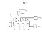
まず、静電容量型のタッチパネル(あるいはタッチセンサ)と呼ばれる入力装置の基本的な動作原理について説明する。図1は、静電容量型のタッチパネル(入力装置)の概要構成を示す説明図である。また、図2は、図1に示すタッチパネルに印加される駆動波形と、タッチパネルから出力される信号波形の関係の例を示す説明図である。また、図3は、図1に示すタッチパネルで、入力位置を検出する時の検出電極周辺の電場の状態を模式的に示す説明図である。また、図4は、図1に示す駆動電極および検出電極の配列の一例を模式的に示す説明図である。また、図5は、図4に示すX方向に沿った断面図である。(Embodiment 1)
<Capacitance type input device>
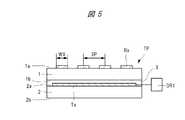
First, a basic operation principle of an input device called a capacitive touch panel (or touch sensor) will be described. FIG. 1 is an explanatory diagram showing a schematic configuration of a capacitive touch panel (input device). FIG. 2 is an explanatory diagram illustrating an example of a relationship between a drive waveform applied to the touch panel illustrated in FIG. 1 and a signal waveform output from the touch panel. FIG. 3 is an explanatory diagram schematically showing the state of the electric field around the detection electrode when the input position is detected by the touch panel shown in FIG. FIG. 4 is an explanatory diagram schematically showing an example of the arrangement of drive electrodes and detection electrodes shown in FIG. FIG. 5 is a cross-sectional view along the X direction shown in FIG.
図1に示すように、静電容量型のタッチパネル(入力装置)TPは、誘電層(中間部材)DLと、誘電層DLを介して対向配置される電極対により構成される複数の容量素子C1を備える。この電極対の一方を構成する駆動電極Txには、入力装置用の駆動回路DR1から、例えば図2に示すような矩形波である駆動波形DWが印加される。一方、電極対の他方を構成する検出電極(入力位置検出電極)Rxからは、例えば図2に示すように駆動波形DW、および図1に示す容量素子C1の静電容量に応じた電流が流れ、信号波形SWが出力される。検出電極Rxから出力された信号波形SWは、入力位置を検出する検出回路DT1(図1参照)に出力される。 As shown in FIG. 1, the capacitive touch panel (input device) TP includes a plurality of capacitive elements C <b> 1 configured by a dielectric layer (intermediate member) DL and an electrode pair disposed to face each other via the dielectric layer DL. Is provided. For example, a drive waveform DW that is a rectangular wave as shown in FIG. 2 is applied to the drive electrode Tx constituting one of the electrode pairs from the drive circuit DR1 for the input device. On the other hand, from the detection electrode (input position detection electrode) Rx constituting the other of the electrode pair, for example, a current corresponding to the drive waveform DW and the capacitance of the capacitive element C1 shown in FIG. 1 flows as shown in FIG. The signal waveform SW is output. The signal waveform SW output from the detection electrode Rx is output to the detection circuit DT1 (see FIG. 1) that detects the input position.
ここで、図3に示すように指やタッチペンなど、一端が接地電位に接続された容量素子(誘電体)である入力具CMDを、入力装置TPの複数の検出電極Rxのうちの一つ(検出電極Rx1)に近づける、または、接触させる。この時、入力具CMDから離れた位置に存在する検出電極Rx2では、駆動電極Txと検出電極Rx2を結ぶ複数の電気力線EFで表わされる電場(電界)が発生する。 Here, as shown in FIG. 3, an input tool CMD, which is a capacitive element (dielectric material) having one end connected to the ground potential, such as a finger or a touch pen, is connected to one of the plurality of detection electrodes Rx of the input device TP ( It is brought close to or in contact with the detection electrode Rx1). At this time, an electric field (electric field) represented by a plurality of electric lines of force EF connecting the drive electrode Tx and the detection electrode Rx2 is generated in the detection electrode Rx2 present at a position away from the input tool CMD.
一方、入力具CMDに近い位置に存在する検出電極Rx1では、容量素子C1に入力具CMDの容量C2が追加される。この場合、図3に示すように、電気力線EFの一部は、駆動電極Txと入力具CMDを結ぶようになるため、検出電極Rx1に繋がる電気力線EFの数は、検出電極Rx2に繋がる電気力線EFの数よりも少なくなる。このため、入力具CMDに近い位置に配置される検出電極Rx1では、他の位置に配置される検出電極Rx2で出力される信号波形SW2よりも小さい信号波形SW1が出力される。 On the other hand, in the detection electrode Rx1 present at a position close to the input tool CMD, the capacitance C2 of the input tool CMD is added to the capacitive element C1. In this case, as shown in FIG. 3, since a part of the electric force lines EF connects the drive electrode Tx and the input tool CMD, the number of electric force lines EF connected to the detection electrode Rx1 is equal to the detection electrode Rx2. The number is less than the number of connected electric field lines EF. For this reason, in the detection electrode Rx1 disposed at a position close to the input tool CMD, a signal waveform SW1 smaller than the signal waveform SW2 output from the detection electrode Rx2 disposed at another position is output.
したがって、図1に示す検出回路DT1では、複数の検出電極Rxのそれぞれから伝送される信号波形SWを監視して、信号波形SWの値、または信号波形SWの変化量に基づいて入力具CMDの位置を特定することができる。例えば、信号波形SWの変化量に予め閾値を設定し、閾値を越えた検出電極Rxの位置データを参照して、入力具CMDの位置を出力することができる。また例えば、信号波形SWの値を直接、閾値と比較することもできる。また、信号波形SWの変化量を監視する方法には、種々の方法があり、例えば、検出電極Rxで発生する電圧値を計測する方法、あるいは、検出回路DT1に流れる単位時間当たりの電流値の積算量を計測する方法を用いることができる。 Therefore, the detection circuit DT1 shown in FIG. 1 monitors the signal waveform SW transmitted from each of the plurality of detection electrodes Rx, and based on the value of the signal waveform SW or the amount of change in the signal waveform SW, The position can be specified. For example, a threshold value can be set in advance for the amount of change in the signal waveform SW, and the position of the input tool CMD can be output with reference to the position data of the detection electrode Rx exceeding the threshold value. Further, for example, the value of the signal waveform SW can be directly compared with a threshold value. There are various methods for monitoring the amount of change in the signal waveform SW, for example, a method of measuring a voltage value generated at the detection electrode Rx, or a current value per unit time flowing through the detection circuit DT1. A method of measuring the integrated amount can be used.
なお、容量素子C1に入力具CMDの容量が追加される現象は、入力具CMDと検出電極Rxが接触した場合以外に、入力具CMDと検出電極Rxが近づいた場合にも発生する。したがって、検出電極Rxは、入力具CMDを配置する面に露出させなくても良く、例えば、検出電極Rxと入力具CMDの間に、カバー部材を配置して検出電極Rxを保護することができる。 Note that the phenomenon that the capacitance of the input tool CMD is added to the capacitive element C1 occurs not only when the input tool CMD and the detection electrode Rx are in contact but also when the input tool CMD and the detection electrode Rx are close to each other. Therefore, the detection electrode Rx may not be exposed on the surface on which the input tool CMD is disposed. For example, a cover member may be disposed between the detection electrode Rx and the input tool CMD to protect the detection electrode Rx. .
また、駆動電極Txと検出電極Rxそれぞれの平面配置は例えば図4に示すような構成になっている。すなわち、図4において、表示平面をXY平面とすると、入力装置TPが備える複数の検出電極Rxは、X方向に沿って間隔(配列間隔、配置間隔)SPで規則的に配列される。また、複数の検出電極Rxのそれぞれは、X方向に沿って幅WXを備え、X方向と直交するY方向に沿って延びるように、帯状に形成される。間隔SPは隣り合う検出電極Rxの中心間距離として規定される。 The planar arrangement of each of the drive electrode Tx and the detection electrode Rx is configured as shown in FIG. 4, for example. That is, in FIG. 4, when the display plane is an XY plane, the plurality of detection electrodes Rx provided in the input device TP are regularly arranged at intervals (arrangement intervals, arrangement intervals) SP along the X direction. Each of the plurality of detection electrodes Rx has a width WX along the X direction and is formed in a strip shape so as to extend along the Y direction orthogonal to the X direction. The interval SP is defined as the distance between the centers of the adjacent detection electrodes Rx.
一方、図4に示す例では、入力装置TPは、複数の駆動電極Txを備えている。複数の駆動電極Txは、検出電極Rxと交差するようにY方向に沿って配列される。また、複数の駆動電極Txのそれぞれは、X方向に沿って延びるように帯状に形成される。このように、複数の駆動電極Txと複数の検出電極Rxを、互いに交差するように配列することで、駆動電極Txと検出電極Rxの交点毎に入力具CMD(図1参照)の有無を判定することができる。例えば、複数の駆動電極Txに順次、駆動波形DW(図2参照)を印加して、平面視における駆動電極Txと検出電極Rxの交点毎に、信号波形SW(図2参照)の値または変化量を判定する。 On the other hand, in the example illustrated in FIG. 4, the input device TP includes a plurality of drive electrodes Tx. The plurality of drive electrodes Tx are arranged along the Y direction so as to intersect with the detection electrodes Rx. Each of the plurality of drive electrodes Tx is formed in a strip shape so as to extend along the X direction. In this way, by arranging the plurality of drive electrodes Tx and the plurality of detection electrodes Rx so as to cross each other, the presence or absence of the input tool CMD (see FIG. 1) is determined for each intersection of the drive electrodes Tx and the detection electrodes Rx. can do. For example, the drive waveform DW (see FIG. 2) is sequentially applied to the plurality of drive electrodes Tx, and the value or change of the signal waveform SW (see FIG. 2) at each intersection of the drive electrode Tx and the detection electrode Rx in plan view. Determine the amount.
また、図4に示す例では、複数の検出電極Rxは前面(面)1a、前面1aの反対側に位置する背面(面、裏面)1bを有する基板1の前面1aに形成される。また、複数の駆動電極Txは、前面(面)2a、前面2aの反対側に位置する背面(面、裏面)2bを有する基板2の前面2aに形成される。そして、複数の検出電極Rxが形成された基板1は、接着層3を介して複数の駆動電極Txが形成された基板2と対向配置され、固定される。 In the example shown in FIG. 4, the plurality of detection electrodes Rx are formed on the
つまり、図4および図5に示す例では、複数の検出電極Rxと駆動電極Txの間に配置される中間部材として、基板1および接着層3が存在する。検出電極Rxと駆動電極Tx間により形成される容量素子C1(図1参照)の静電容量は、検出電極Rxと駆動電極Tx間の距離、検出電極Rxの面積、および中間部材の比誘電率により規定される。したがって、図4および図5に示す入力装置TPの場合には、基板1および接着層3の比誘電率が容量素子C1の静電容量に影響する。 That is, in the example shown in FIGS. 4 and 5, the
<入力位置検出精度>
次に、入力装置TPの位置検出精度(入力位置検出の正確さ)について説明する。図6は、入力装置の位置検出精度について、入力位置検出電極の幅の最適値(理想値)を算出する座表面を示す説明図である。<Input position detection accuracy>
Next, the position detection accuracy (input position detection accuracy) of the input device TP will be described. FIG. 6 is an explanatory diagram showing a seat surface for calculating the optimum value (ideal value) of the width of the input position detection electrode with respect to the position detection accuracy of the input device.
入力装置TPの入力位置検出の正確さを規定する要因として、解像度(検出箇所の細かさ)と、検出感度(誤検出や不検出の少なさ)がある。この解像度と検出感度がともに上昇すれば、入力位置検出の正確さが向上する。この入力位置の正確さは、位置検出誤差(Accuracy error)と呼ばれる指標を用いて表すことができる。この位置検出誤差の指標は、実際の入力位置と検出された入力位置の誤差を距離で表わす指標であって、一般に、小型〜中型のタッチパネルでは、位置検出誤差は±2.0mm以下が好ましいとされる。 Factors that define the accuracy of detection of the input position of the input device TP include resolution (fineness of a detected portion) and detection sensitivity (smallness of false detection and non-detection). If both the resolution and the detection sensitivity increase, the accuracy of input position detection is improved. The accuracy of the input position can be expressed using an index called a position detection error (Accuracy error). The index of the position detection error is an index representing an error between the actual input position and the detected input position as a distance. Generally, in a small to medium touch panel, the position detection error is preferably ± 2.0 mm or less. Is done.
上記した解像度および検出感度は、複数の検出電極Rxの幅WXおよび間隔SPにより大きく変化する。まず、単位面積当たりの検出箇所を増加させる程、解像度が向上する。このため、解像度を向上させる観点からは、図4および図5に示す複数の検出電極Rxの間隔SPを狭くして、検出箇所を増加させることが好ましい。一方、入力装置TPでは、前記したように、図2や図3に示す信号波形SWの値、あるいは信号波形SWの変化量を計測することにより入力位置を検出する。このため、信号波形SWが大きくなれば、誤検出や不検出の頻度が低下し、検出感度が上昇する。したがって、図4および図5に示す複数の検出電極Rxの間隔SPを広くして(隣り合う検出電極Rxの間の空間を広くして)、隣り合う検出電極Rxの間を電気力線EF(図3参照)が通過し易くすることが好ましい。 The resolution and detection sensitivity described above vary greatly depending on the width WX and the interval SP of the plurality of detection electrodes Rx. First, as the number of detection points per unit area is increased, the resolution is improved. For this reason, from the viewpoint of improving the resolution, it is preferable to increase the number of detection points by narrowing the interval SP between the plurality of detection electrodes Rx shown in FIGS. On the other hand, as described above, the input device TP detects the input position by measuring the value of the signal waveform SW shown in FIGS. 2 and 3 or the change amount of the signal waveform SW. For this reason, if the signal waveform SW becomes large, the frequency of erroneous detection and non-detection decreases, and the detection sensitivity increases. Therefore, the interval SP between the plurality of detection electrodes Rx shown in FIGS. 4 and 5 is widened (the space between the adjacent detection electrodes Rx is widened), and the electric lines of force EF ( It is preferable to make it easy to pass.
すなわち、入力位置検出の正確さを規定する要因である解像度と検出感度は、検出電極Rxの間隔SPにより大きく変化し、かつ、トレードオフの関係にある。また、検出電極Rxの幅WXの値は、間隔SPの値に対応して最適値がある。ここで、検出電極Rxの間隔SPは、検出対象物である入力具CMDに応じて決定される。例えば、一般に2mm〜6mm程度の間隔になる。このため、位置検出誤差を±2.0mm以下に収めるためには、検出電極Rxの幅WXを適正な値に調整する必要があることが判った。ところが、検出感度は、検出電極Rxと駆動電極Txの間に配置される中間部材の厚さや比誘電率にも影響を受けるため、製品種類毎に検出電極Rxの幅WXの最適値(理想値)が異なり、調整が困難である。 That is, the resolution and detection sensitivity, which are factors that determine the accuracy of input position detection, vary greatly depending on the interval SP between the detection electrodes Rx, and are in a trade-off relationship. Further, the value of the width WX of the detection electrode Rx has an optimum value corresponding to the value of the interval SP. Here, the interval SP of the detection electrodes Rx is determined according to the input tool CMD that is the detection target. For example, the interval is generally about 2 mm to 6 mm. For this reason, it was found that the width WX of the detection electrode Rx must be adjusted to an appropriate value in order to keep the position detection error within ± 2.0 mm. However, since the detection sensitivity is also affected by the thickness and relative dielectric constant of the intermediate member disposed between the detection electrode Rx and the drive electrode Tx, the optimum value (ideal value) of the width WX of the detection electrode Rx for each product type. ) Is different and adjustment is difficult.
そこで、本願発明者は、検出電極Rxの幅WXの最適値(理想値)を容易に算出する技術について検討を行った。この結果、検出電極Rxの間隔SPを決定すれば、検出電極Rxの幅WXの最適値は、実効電極間距離(中間部材(図4の場合は基板1および接着層3)の比誘電率を前記中間部材の厚さで除した値の逆数)の関数として表わせることを見出した。また、上記した実効電極間距離を決定すれば、検出電極Rxの幅WXの最適値は、検出電極Rxの間隔SPの関数として表わせることを見出した。そして、上記した実効電極間距離の関数式と間隔SPの関数式を組み合わせて、以下の算出式を見出した。 Accordingly, the inventors of the present application have studied a technique for easily calculating the optimum value (ideal value) of the width WX of the detection electrode Rx. As a result, if the interval SP of the detection electrodes Rx is determined, the optimum value of the width WX of the detection electrodes Rx is the effective inter-electrode distance (the relative permittivity of the intermediate member (the
すなわち、図4に示す複数の検出電極Rxそれぞれの、X方向の幅の理想値をWsmax[μm]とする。また、複数の検出電極Rxのうち、隣り合う検出電極Rxの中心間距離である間隔SPをP[μm]とする。また、中間部材(図4の場合は基板1および接着層3)の比誘電率を前記中間部材の厚さで除した値の逆数で表わされる実効電極間距離をD[μm]とする。この時、
Wsmax=0.488×P−4.33×D−160 ・・・(式1)
の式が成り立つことを見出した。That is, the ideal value of the width in the X direction of each of the plurality of detection electrodes Rx shown in FIG. 4 is set to Wsmax [μm]. Further, among the plurality of detection electrodes Rx, an interval SP that is the distance between the centers of the adjacent detection electrodes Rx is P [μm]. In addition, the effective inter-electrode distance represented by the reciprocal of the value obtained by dividing the relative dielectric constant of the intermediate member (in the case of FIG. 4, the
Wsmax = 0.488 × P−4.33 × D-160 (Formula 1)
We found that the following formula holds.
上記(式1)は、図6に示す座標面Smaxの関数式であって、図4に示す幅WX、間隔SP、および検出電極Rxと駆動電極Txの実効電極間距離の値は、図6に示す座表面Smax上にプロットされる時に最適値になることを示している。言い換えれば、図4に示す幅WX、間隔SP、および検出電極Rxと駆動電極Txの実効電極間距離という3変数のうち、2変数の値を決定すれば、残る1変数の最適値は(式1)により容易に導くことができる。 The above (Expression 1) is a functional expression of the coordinate plane Smax shown in FIG. 6, and the values of the width WX, the interval SP, and the effective interelectrode distance between the detection electrode Rx and the drive electrode Tx shown in FIG. It shows that the optimum value is obtained when plotted on the seating surface Smax shown in FIG. In other words, if two variables are determined among the three variables of the width WX, the interval SP, and the effective distance between the detection electrode Rx and the drive electrode Tx shown in FIG. It can be easily guided by 1).
また、図4や図5に示すように、検出電極Rxと駆動電極Txの間に複数の中間部材が設けられる場合、上記(式1)における実効電極間距離の値は、以下のように求められる。すなわち、図5に示す基板1の比誘電率をε1、基板1の厚さをd1とし、接着層3の比誘電率をε3、基板1の厚さをd3とすると、
D=1/(ε1/d1+ε3/d3) ・・・(式2)
の式により表わせる。Further, as shown in FIGS. 4 and 5, when a plurality of intermediate members are provided between the detection electrode Rx and the drive electrode Tx, the value of the effective interelectrode distance in the above (Expression 1) is obtained as follows. It is done. That is, when the relative dielectric constant of the
D = 1 / (ε1 / d1 + ε3 / d3 ) (Expression 2)
It can be expressed by the following formula.
また、上記(式2)をn層の中間部材が配置されている場合の式として一般化すると、 Moreover, when the above (Formula 2) is generalized as a formula when n-layer intermediate members are arranged,

の式により表わせる。つまり、複数層の中間部材それぞれの、比誘電率を厚さで除した値の和の逆数として表わされる。 It can be expressed by the following formula. That is, it is expressed as the reciprocal of the sum of the values obtained by dividing the relative dielectric constant by the thickness of each of the intermediate members of the plurality of layers.
つまり、本実施の形態によれば、検出電極Rxと駆動電極Txの間に例えば多数の中間部材が設けられるような複雑な構造の入力装置であっても、各中間部材の厚さおよび比誘電率を把握することで、容易に上記(式1)に代入する実効電極間距離の値を算出することができる。 That is, according to the present embodiment, even in an input device having a complicated structure in which a large number of intermediate members are provided between the detection electrode Rx and the drive electrode Tx, the thickness and relative dielectric constant of each intermediate member By grasping the rate, it is possible to easily calculate the value of the effective interelectrode distance that is substituted into the above (Equation 1).
上記のように、本実施の形態によれば、幅WX、間隔SP、および検出電極Rxと駆動電極Txの実効電極間距離という3変数のうち、2変数の値を決定すれば、残る1変数の最適値は(式1)により容易に導くことができる。このため、大きさや構造の異なる様々な製品について、幅WX、間隔SP、および検出電極Rxと駆動電極Txの実効電極間距離の最適な関係を容易に設計することができる。 As described above, according to the present embodiment, if the value of two variables among the three variables of the width WX, the interval SP, and the effective interelectrode distance between the detection electrode Rx and the drive electrode Tx is determined, the remaining one variable The optimum value of can be easily derived from (Equation 1). For this reason, the optimal relationship among the width WX, the distance SP, and the effective interelectrode distance between the detection electrode Rx and the drive electrode Tx can be easily designed for various products having different sizes and structures.
<実製品の許容範囲>
上記したように、幅WX、間隔SP、および検出電極Rxと駆動電極Txの実効電極間距離が、上記(式1)の関係を満たす時に、入力装置TPの入力位置検出精度は最も高くなるが、実際の製品に適用する場合には、加工精度上の問題、あるいは他の設計条件の制約などにより、図6に示す座表面Smaxからずれる場合がある。そこで、本願発明者は、位置検出誤差を±2.0mm以下にする観点から許容される、座表面Smaxからのずれ量について検討した。以下、図4および図5に示す検出電極Rxの幅WXを取り上げて、(式1)に示すWsmaxに対する許容誤差について説明する。図7は、図4および図5に示す検出電極の幅の、最適値(理想値)との差と、位置検出精度の関係を示す説明図である。<Acceptable range of actual product>
As described above, when the width WX, the interval SP, and the effective inter-electrode distance between the detection electrode Rx and the drive electrode Tx satisfy the relationship of (Expression 1), the input position detection accuracy of the input device TP is the highest. When applied to an actual product, the seat surface Smax shown in FIG. 6 may deviate due to a problem in processing accuracy or restrictions on other design conditions. Therefore, the inventor of the present application examined the deviation amount from the seat surface Smax that is allowed from the viewpoint of setting the position detection error to ± 2.0 mm or less. Hereinafter, the allowable error with respect to Wsmax shown in (Formula 1) will be described by taking up the width WX of the detection electrode Rx shown in FIGS. FIG. 7 is an explanatory diagram showing the relationship between the difference between the detection electrode width shown in FIGS. 4 and 5 and the optimum value (ideal value) and the position detection accuracy.
図7に示す評価結果は、図4および図5に示す検出電極Rxの幅WXを変化させて、幅WXの理想値からのずれ(WX−Wsmax)と、検出精度の相関を調査した結果を示している。なお、図7に示す評価では、間隔Pおよび実効電極間距離Dが異なる2種類の入力装置を準備してそれぞれに検出電極Rxの幅WXを変化させて評価した。評価指標として、入力位置の位置検出誤差(Accuracy error)を用いた。図7では単に検出誤差と記載している。また、評価の欄では、検出誤差が±1.5mm以下の場合○を、検出誤差が±1.5mm〜±2.0mmの時△を、検出誤差が±2.0mmを越える場合には×を付している。 The evaluation results shown in FIG. 7 are obtained by changing the width WX of the detection electrode Rx shown in FIG. 4 and FIG. Show. In the evaluation shown in FIG. 7, two types of input devices having different distances P and effective interelectrode distances D were prepared, and the width WX of the detection electrode Rx was changed and evaluated. The position detection error (Accuracy error) of the input position was used as an evaluation index. In FIG. 7, it is simply described as a detection error. Also, in the evaluation column, ○ when the detection error is ± 1.5 mm or less, Δ when the detection error is ± 1.5 mm to ± 2.0 mm, and × when the detection error exceeds ± 2.0 mm. Is attached.
図7に示す評価結果より、幅WXの理想値からのずれ(WX−Wsmax)の絶対値が150μm以下の範囲内であれば、検出誤差を2.0mm以下にできることが判った。言い換えれば、図4に示す複数の検出電極Rxそれぞれの、X方向の幅WXを、Wsmaxの値±150μm以内の範囲に収めることで、様々な種類の入力装置の入力位置検出感度および解像度を、それぞれ向上させることができる。また、より確実に検出誤差を±2.0mm以内に収める観点からは、幅WXを、Wsmaxの値±100μm以内の範囲に収めることが特に好ましいことが判った。 From the evaluation results shown in FIG. 7, it was found that the detection error can be reduced to 2.0 mm or less if the absolute value of the deviation (WX−Wsmax) from the ideal value of the width WX is within a range of 150 μm or less. In other words, by setting the width WX in the X direction of each of the plurality of detection electrodes Rx shown in FIG. 4 within the range of the value of Wsmax ± 150 μm, the input position detection sensitivity and resolution of various types of input devices can be obtained. Each can be improved. Further, it has been found that it is particularly preferable to set the width WX within the range of the value of Wsmax ± 100 μm from the viewpoint of more surely keeping the detection error within ± 2.0 mm.
<入力装置の変形例>
図1〜図7では、判り易さのため、シンプルな構造の入力装置TPについて説明したが、入力装置として機能させる観点からは、離間して設けられた検出電極Rxと駆動電極Txの間に中間部材が設けられていれば良いので、図8および図9に例示的に示すように種々の変形例に適用することができる。図8は図5に対する変形例である入力装置を示す断面図である。図9は、図4に示す電極レイアウトに対する変形例である入力装置を示す説明図である。<Modification of input device>
In FIG. 1 to FIG. 7, the input device TP having a simple structure has been described for the sake of easy understanding. However, from the viewpoint of functioning as an input device, a space between the detection electrode Rx and the drive electrode Tx provided apart from each other is described. Since the intermediate member only needs to be provided, the present invention can be applied to various modified examples as illustrated in FIGS. 8 and 9. FIG. 8 is a cross-sectional view showing an input device which is a modification to FIG. FIG. 9 is an explanatory diagram showing an input device which is a modification of the electrode layout shown in FIG.
図8に示す入力装置TP1は、例えばガラス基板などの誘電体である基板1の前面1aに複数の検出電極Rxが、前面1aの反対側に位置する背面1bには検出電極Rxとの間で容量素子を形成する駆動電極Txが形成される。つまり、検出電極Rxと駆動電極Txの間に配置される中間部材は複数層には限定されず、1層構造であっても前述した技術を適用することができる。また、図5に示す入力装置TPや図8に示す入力装置TP1では検出電極Rxが露出しているが、検出電極Rxを露出させた構造には限定されない。図示は省略するが、例えば、ガラス基板など、基板1とは別の基板(カバー部材)を図5に示す複数の検出電極Rxを覆うように、基板1の前面1a側に配置することができる。この場合、検出電極Rxを損傷から保護することができる。 An input device TP1 shown in FIG. 8 includes a plurality of detection electrodes Rx on a
また、図9に示す入力装置TP2は、駆動電極Txはベタパターンとされ、検出電極Rxを行列状(マトリクス状)に配置される。この場合、四角形を成す検出電極Rxの一つの辺が延びる方向(図9ではY方向)について、幅WXおよび間隔SPを定義すれば、図4を用いて説明した(式1)と同様に適用することができる。 Further, in the input device TP2 shown in FIG. 9, the drive electrode Tx has a solid pattern, and the detection electrodes Rx are arranged in a matrix (matrix). In this case, if the width WX and the interval SP are defined in the direction in which one side of the quadrangular detection electrode Rx extends (the Y direction in FIG. 9), the same applies as in (Expression 1) described with reference to FIG. can do.
(実施の形態2)
前記実施の形態1では、入力装置TP、TP1、TP2の構造について説明したが、タッチパネルと呼ばれる入力装置は、表示画像に基づいて入力指示を行うので、入力装置と表示装置を組み合わせて使用される。本実施の形態では、入力装置と表示装置を組み合わせた入力装置付き表示装置に前記実施の形態1で説明した技術を適用した場合の実施態様について説明する。また、以下の実施の形態では、表示装置の例として、表示用の電極間に表示用電圧が印加されることで表示画像を形成する表示機能層として、液晶層を用いる液晶表示装置を取り上げて説明する。(Embodiment 2)
In the first embodiment, the structure of the input devices TP, TP1, and TP2 has been described. However, an input device called a touch panel issues an input instruction based on a display image, and thus the input device and the display device are used in combination. . In the present embodiment, an embodiment will be described in the case where the technique described in the first embodiment is applied to a display device with an input device in which the input device and the display device are combined. In the following embodiments, as an example of a display device, a liquid crystal display device using a liquid crystal layer as a display functional layer that forms a display image by applying a display voltage between display electrodes is taken up. explain.
<表示装置の基本構成>
次に、表示装置の基本構成について説明する。図10は、液晶表示装置の一例の基本構成を示す要部断面図である。なお、図10では、見易さのため、液晶層16についてはハッチングを省略し、液晶層16を構成する液晶LCを模式的に楕円形で示している。<Basic configuration of display device>
Next, the basic configuration of the display device will be described. FIG. 10 is a cross-sectional view of a principal part showing a basic configuration of an example of a liquid crystal display device. In FIG. 10, for ease of viewing, hatching is omitted for the
液晶表示装置は、表示機能層である液晶層の液晶分子の配向を変化させるための電界の印加方向により、大きくは以下の2通りに分類される。すなわち、第1の分類として、液晶表示装置の厚さ方向(面外方向)に電界が印加される、所謂、縦電界モードがある。縦電界モードには、例えばTN(twisted Nematic)モードや、VA(Vertical Alignment)などがある。また、第2の分類として、液晶表示装置の平面方向(面内方向)に電界が印加される、所謂、横電界モードがある。横電界モードには、例えばIPS(In-Plane Switching)モードや、FFS(Fringe Field Switching)モードなどがある。以下で説明する技術は、縦電界モードおよび横電界モードのいずれにも適用できるが、図10では、一例として、横電界モード(詳しくはFFSモード)の表示装置を示している。 Liquid crystal display devices are roughly classified into the following two types according to the application direction of an electric field for changing the orientation of liquid crystal molecules in a liquid crystal layer as a display function layer. That is, as a first classification, there is a so-called vertical electric field mode in which an electric field is applied in the thickness direction (out-of-plane direction) of the liquid crystal display device. Examples of the vertical electric field mode include a TN (twisted nematic) mode and a VA (Vertical Alignment). As a second category, there is a so-called lateral electric field mode in which an electric field is applied in the planar direction (in-plane direction) of the liquid crystal display device. Examples of the transverse electric field mode include an IPS (In-Plane Switching) mode and an FFS (Fringe Field Switching) mode. Although the technique described below can be applied to both the vertical electric field mode and the horizontal electric field mode, FIG. 10 shows a display device in the horizontal electric field mode (specifically, the FFS mode) as an example.
図10に示す表示装置LCD1は、表示面側(観者VW側)に配置される前面(面)11aを有する基板11、および基板11の前面11aの反対側に、基板11と離間して配置される基板12を備える。また、表示装置LCD1は、基板11と基板12の間に配置される複数の画素電極13、および基板11と基板12の間に配置される共通電極14を備える。また、表示装置LCD1は、基板11と基板12の間に配置され、複数の画素電極13と共通電極14との間に表示用電圧が印加されることで表示画像を形成する表示機能層である液晶層16を備える。 A display device LCD1 shown in FIG. 10 is disposed with a
基板11は、カラー表示の画像を形成するカラーフィルタ(図示は省略)が形成されたカラーフィルタ基板であって、表示面側である前面11aおよび前面11aの反対側に位置する背面(面、裏面、内面)11bを有する。基板11は、例えばガラス基板などの基材の一方の面に、赤(R)、緑(G)、青(B)の3色のカラーフィルタ層を周期的に配列して構成されたカラーフィルタが貼り付けられている。カラー表示装置では、例えばこの赤(R)、緑(G)、青(B)の3色のサブピクセルを1組として、1画素(1ピクセル)を構成する。 The
また、基板(アレイ基板)12は、主として画像表示用の回路が形成された回路基板であって、基板11側に位置する前面(面、内面)12aおよびその反対側に位置する背面(面、裏面)12bを有する。基板12の前面12a側には、TFT(Thin-Film Transistor)などのアクティブ素子と、複数の画素電極13がマトリクス状(アレイ状)に形成されている。また、図10に示す例は、前記したように横電界モード(詳しくはFFSモード)の表示装置LCD1を示しているので、共通電極14も基板12の前面12a側に形成されている。共通電極14は、基板12の前面12a上に形成され、共通電極14上には絶縁層15が積層される。また、複数の画素電極13は、絶縁層15を介して共通電極14と対向するように絶縁層15上に形成される。表示装置LCD1では、表示期間において、画素電極13には画素電圧が、共通電極14には共通駆動信号がそれぞれ印加され、これにより各画素の表示電圧が画定される。 The substrate (array substrate) 12 is a circuit substrate on which an image display circuit is mainly formed, and includes a front surface (surface, inner surface) 12a positioned on the
また、図示は省略するが、基板12には、上記の他、画素電極13を駆動するための表示ドライバや画素電極13に画素信号を供給するソース線や、TFTを駆動するゲート線等の配線が形成されている。 Although not shown, the
また、基板11と基板12の間には、画素電極13と共通電極14との間に表示用電圧が印加されることで表示画像を形成する表示機能層である、液晶層16が設けられる。液晶層16は、印加された電界の状態に応じてそこを通過する光を変調するものであり、例えば、TN、VA、FFS等の各種モードに対応した液晶LCが用いられる。なお、図示は省略するが、液晶層16と基板11、12の間には、それぞれ配向膜が形成されている。 In addition, a
また、表示装置LCD1の基板12の背面12b側には、光源LSおよび、光源LSから発生した光をフィルタリングする偏光板PL1が設けられる。一方、基板11の前面11a側には、基板11を通過した光をフィルタリングする偏光板PL2が設けられる。 A light source LS and a polarizing plate PL1 that filters light generated from the light source LS are provided on the
また、図10に示す例では、基板12の前面12aに、画素電極13に駆動電位を供給する駆動回路が形成された半導体チップ(ドライバチップ)17、および画像表示用の駆動回路DR2と電気的に接続された配線基板18が電気的に接続されている。配線基板18は、例えば、樹脂フィルム内に複数の配線が形成され、配置場所の形状に応じて自在に変形させることができる、所謂フレキシブル配線板である。配線基板18に形成される配線には、画素電極13と電気的に接続される配線18a、および共通電極14と電気的に接続される配線18bが含まれる。なお、図10に示す例では、基板12上に半導体チップを実装する、所謂COG(Chip on glass)方式の実施態様を例示しているが、半導体チップを実装する場所は基板12上には限定されず、例えば配線基板18に実装する方式を適用することもできる。 In the example shown in FIG. 10, a semiconductor chip (driver chip) 17 in which a driving circuit for supplying a driving potential to the
図10に示す表示装置LCD1によるカラー画像の表示方法は、例えば以下の通りである。すなわち、光源LSから出射された光は、偏光板PL1によってフィルタリングされ、偏光板PL1を通過する振幅を有する光(偏光)が液晶層16に入射する。液晶層16に入射した光は、液晶LCの屈折率異方性(複屈折)に応じて偏光状態を変化させて液晶層16の厚さ方向(基板12から基板11に向かう方向)に伝搬され、基板11から出射される。この時、画素電極13と共通電極14に電圧を印加して形成される電界により、液晶配向が制御され、液晶層16は光学的なシャッターとして機能する。つまり、液晶層16において、サブピクセル毎に光の透過率を制御することができる。基板11に到達した光は、基板11に形成されたカラーフィルタにおいて、色フィルタリング処理(所定の波長以外の光を吸収する処理)が施され、前面11aから出射される。また、前面11aから出射された光は、偏光板PL2によってフィルタリングされ観者VWに到達する。 The display method of the color image by the display device LCD1 shown in FIG. 10 is, for example, as follows. That is, the light emitted from the light source LS is filtered by the polarizing plate PL1, and light (polarized light) having an amplitude passing through the polarizing plate PL1 enters the
<入力装置付き表示装置の構成>
次に、上記した入力装置の機能と、表示装置の機能を組み合わせた、入力装置付き表示装置の構成について説明する。図11は、図4に示す入力装置と図10に示す表示装置を組み合わせた入力装置付き表示装置の構成例を示す要部断面図である。また、図12は、図11に対する変形例である入力装置付き表示装置の一例の基本構成を示す要部断面図である。なお、図11および図12は図4に示すY方向に沿った断面に対応するので、検出電極Rxは1本の長い導体パターンとして図示されている。<Configuration of display device with input device>
Next, the configuration of a display device with an input device that combines the functions of the input device and the display device will be described. 11 is a cross-sectional view of an essential part showing a configuration example of a display device with an input device in which the input device shown in FIG. 4 and the display device shown in FIG. 10 are combined. FIG. 12 is a cross-sectional view of an essential part showing a basic configuration of an example of a display device with an input device, which is a modified example of FIG. 11 and 12 correspond to the cross section along the Y direction shown in FIG. 4, the detection electrode Rx is shown as one long conductor pattern.
単純構造の入力装置付き表示装置としては、図11に示す入力装置付き表示装置LCD2のように、表示装置LCD1の偏光板PL2上に入力装置TPを配置した実施態様を適用できる。入力装置付き表示装置LCD2は、表示装置LCD1の基板11側の偏光板PL2と入力装置TPの基板2を対向配置し、接着層BDを介して接着固定している。前記実施の形態1で説明した技術は、入力装置付き表示装置LCD2にも適用できるが、図12に示す入力装置付き表示装置LCD3のように、検出電極Rxと駆動電極Txの間に多数の部材が積層されるような入力装置付き表示装置に適用して特に有効である。 As a display device with an input device having a simple structure, an embodiment in which the input device TP is arranged on the polarizing plate PL2 of the display device LCD1, such as a display device LCD2 with an input device shown in FIG. 11, can be applied. In the display device LCD2 with an input device, the polarizing plate PL2 on the
図12に示す入力装置付き表示装置LCD3は、図10を用いて説明した表示装置LCD1の基板11側に、検出電極(入力位置検出電極)Rxが形成され、駆動電極Txは形成されていない。検出電極Rxには、配線基板23が接続され、配線基板23を介して、入力位置を検出する検出回路DT1と電気的に接続される。配線基板23は、例えば、樹脂フィルム内に複数の配線が形成され、配置場所の形状に応じて自在に変形させることができる、所謂フレキシブル配線板である。配線基板23に形成される配線には、複数の検出電極Rxと電気的に接続され、検出信号を検出回路DT1に伝送する配線23aが含まれる。 In the display device LCD3 with an input device shown in FIG. 12, the detection electrode (input position detection electrode) Rx is formed on the
入力装置付き表示装置LCD3では、図12に示すように、表示装置LCD1の共通電極14に、図2を用いて説明した入力位置検出用の駆動波形DWを印加する。共通電極14には、例えば配線基板18を介して駆動波形DW(図2参照)を印加することができる。共通電極14は、配線基板18を介して、駆動回路DR1と電気的に接続されている。 In the display device LCD3 with the input device, as shown in FIG. 12, the drive waveform DW for detecting the input position described with reference to FIG. 2 is applied to the
上記のように、共通電極14に入力位置検出用の駆動波形DWを印加する構成を別の表現で表わせば、入力装置付き表示装置LCD3では、共通電極14は、表示装置LCD1用の共通電極14としての機能と、入力装置の駆動電極Txとしての機能を兼用する電極になっている。共通電極14と駆動電極Txを兼用化する方法としては、例えば、ある期間(1期間)をタッチ検出期間(入力期間)と、ディスプレイ書込み期間に分けることで実現できる。このように、表示装置LCD1用の共通電極14と入力装置の駆動電極Txを兼用化することで、入力装置付き表示装置LCD3の全体の厚さを薄型化することができる。 As described above, if the configuration for applying the drive waveform DW for detecting the input position to the
入力装置付き表示装置LCD3では、表示面側の偏光板PL2とカラーフィルタが形成された基板11の間に検出電極Rxが形成されている。言い換えれば、入力装置付き表示装置LCD3では、入力装置としての検出電極Rxおよび駆動電極Txが、対向配置される偏光板PL1、PL2の間、つまり表示装置LCD1の内部に形成されている。このように表示装置の内部に入力装置としての検出電極Rxおよび駆動電極Txを形成することで、入力装置付き表示装置の厚さは最も薄型化することができる。 In the display device LCD3 with an input device, the detection electrode Rx is formed between the polarizing plate PL2 on the display surface side and the
図12では、表示装置LCD1用の共通電極14と入力装置の駆動電極Txを兼用化する実施態様の例として、表示面側の偏光板PL2とカラーフィルタが形成された基板11の間に検出電極Rxが形成された入力装置付き表示装置LCD3を示している。しかし、検出電極Rxは、基板11を挟んで、かつ基板12の反対側であれば、形成位置は種々の変形例を適用できる。例えば図12に示す基板21は、基板11の前面11aと対向する背面21b、および背面21bの反対側に位置する前面21aを有するカバー板である。図12に対する変形例としては、この基板21の前面21aまたは背面21bのうち、少なくともいずれか一方の面に形成することができる。あるいは、基板21と基板11の間に、少なくとも一方の面に検出電極Rxが形成された基板(図示は省略)を追加することができる。 In FIG. 12, as an example of an embodiment in which the
入力装置付き表示装置3のように表示装置LCD1用の共通電極14と入力装置の駆動電極Txを兼用化すると、検出電極Rxと駆動電極Txの間に中間部材が多く配置されるため、検出電極Rxの電極幅と、配置間隔、検出電極Rxと駆動電極Txの間の実効電極間距離の値を最適化することが難しくなる。しかし、前記実施の形態1で説明した(式3)を適用することにより、検出電極Rxと駆動電極Txの間の実効電極間距離Dを容易に算出することができる。すなわち、図12に示す入力装置付き表示装置LCD3の場合であれば、基板11、液晶層16、画素電極13、および絶縁層15のそれぞれの厚さおよび比誘電率を(式3)に代入することで実効電極間距離Dの値を容易に算出することができる。また、算出した実効電極間距離Dの値を(式1)に代入することにより、Wsmaxと間隔Pの一元方程式が得られる。つまり、図4を用いて説明した間隔SPと幅WXのうち、いずれか一方を決定すれば、他方の最適値(理想値)を容易に算出することができる。また、前記実施の形態1で説明したように、図4に示す複数の検出電極Rxそれぞれの、X方向の幅WXを、Wsmaxの値±150μm以内の範囲に収めることで、様々な種類の入力装置の入力位置検出感度および解像度を、それぞれ向上させることができる。また、より確実に検出誤差を±2.0mm以内に収める観点からは、幅WXを、Wsmaxの値±100μm以内の範囲に収めることが好ましい。 When the
<その他の変形例>
以上、本願発明者によってなされた発明を実施の形態に基づき具体的に説明したが、本発明は前記実施の形態に限定されるものではなく、その要旨を逸脱しない範囲で種々変更可能である。<Other variations>
As mentioned above, although the invention made by the inventor of the present application has been specifically described based on the embodiments, the present invention is not limited to the above-described embodiments, and various modifications can be made without departing from the scope of the invention.
例えば、前記実施の形態では、検出電極Rxの最適な幅であるWsmaxを算出する式を(式1)として示したが、検出電極Rxの線幅を定数にして、他の変数(実効電極間距離Dまたは間隔P)を算出する式とすることができる。 For example, in the above embodiment, the formula for calculating Wsmax, which is the optimum width of the detection electrode Rx, is shown as (Formula 1). However, the line width of the detection electrode Rx is set as a constant, and other variables (between the effective electrodes) It can be an expression for calculating the distance D or the interval P).
また例えば、前記実施の形態1および前記実施の形態2で説明した技術を、液晶表示装置の他、有機EL(Electro-Luminescence)ディスプレイなどの表示装置に適用することができる。 For example, the technique described in the first and second embodiments can be applied to a display device such as an organic EL (Electro-Luminescence) display in addition to a liquid crystal display device.
本発明は、入力装置付きの表示装置や入力装置付き表示装置が組み込まれた電子機器に広く適用することができる。 The present invention can be widely applied to a display device with an input device and an electronic apparatus in which the display device with an input device is incorporated.
1、2 基板
1a、2a 前面(面)
1b、2b 背面(面、裏面)
3 接着層
11 基板(カラーフィルタ基板)
11a 前面(面)
11b 背面(面、裏面、内面)
12 基板(アレイ基板)
12a 前面(面、内面)
12b 背面(面、裏面)
13 画素電極
14 共通電極
15 絶縁層
16 液晶層
17 半導体チップ(ドライバチップ)
18 配線基板
18a、18b 配線
19 接着層
20 タッチ検出基材
21 基板
21a 前面(面)
21b 背面(面、裏面)
23 配線基板
23a 配線
BD 接着層
C1 容量素子
C2 容量
CMD 入力具
DL 誘電層(中間部材)
DR1 駆動回路(入力装置用駆動回路)
DR2 駆動回路(表示用駆動回路)
DT1 検出回路
DW 駆動波形
EF 電気力線
LC 液晶
LCD1 表示装置
LCD2、LCD3 入力装置付き表示装置
LS 光源
PL1、PL2 偏光板
Rx、Rx1、Rx2 検出電極(入力位置検出電極)
Smax 座表面
SP 間隔(配列間隔、配置間隔)
SW、SW1、SW2 信号波形
TP、TP1、TP2 入力装置(タッチパネル)
Tx 駆動電極
VW 観者
WX 幅1, 2
1b, 2b Back (surface, back)
3
11a Front (surface)
11b Back surface (surface, back surface, inner surface)
12 Substrate (array substrate)
12a Front (surface, inner surface)
12b Back (surface, back)
13
18
21b Rear surface (surface, back surface)
23
DR1 drive circuit (input device drive circuit)
DR2 drive circuit (display drive circuit)
DT1 Detection circuit DW Drive waveform EF Electric field line LC Liquid crystal LCD1 Display device LCD2, LCD3 Display device with input device LS Light source PL1, PL2 Polarizing plate Rx, Rx1, Rx2 Detection electrode (input position detection electrode)
Smax Seat surface SP interval (arrangement interval, arrangement interval)
SW, SW1, SW2 Signal waveform TP, TP1, TP2 Input device (touch panel)
Tx Drive electrode VW Viewer WX width
Claims (5)
Translated fromJapanese前記複数の入力位置検出電極と対向するように配置され、前記複数の入力位置検出電極との間で静電容量を形成する駆動電極と、
前記複数の入力位置検出電極と前記駆動電極の間に配置される中間部材と、
を備え、
前記複数の入力位置検出電極それぞれの、前記第1方向の幅の理想値をWsmax[μm]とし、
前記複数の入力位置検出電極のうち、隣り合う入力位置検出電極の中心間距離である前記第1間隔をP[μm]とし、
前記中間部材の比誘電率を前記中間部材の厚さで除した値の逆数で表わされる実効電極間距離をD[μm]とすると、
Wsmax=0.488×P−4.33×D−160
で表わされ、
前記複数の入力位置検出電極それぞれの、前記第1方向の幅は、前記Wsmaxの値±150μm以内の範囲に収まる入力装置。A plurality of input position detection electrodes arranged at a first interval along a first direction of the display plane;
A drive electrode that is arranged to face the plurality of input position detection electrodes and forms a capacitance with the plurality of input position detection electrodes;
An intermediate member disposed between the plurality of input position detection electrodes and the drive electrode;
With
The ideal value of the width in the first direction of each of the plurality of input position detection electrodes is Wsmax [μm],
Of the plurality of input position detection electrodes, the first interval, which is the distance between the centers of adjacent input position detection electrodes, is P [μm],
When the effective inter-electrode distance represented by the reciprocal of the value obtained by dividing the relative dielectric constant of the intermediate member by the thickness of the intermediate member is D [μm],
Wsmax = 0.488 × P−4.33 × D-160
Represented by
The input device in which the width in the first direction of each of the plurality of input position detection electrodes is within the range of the value of Wsmax ± 150 μm.
前記比誘電率の異なる複数の前記中間部材それぞれの、比誘電率を厚さで除した値の和の逆数として表わされる請求項1に記載の入力装置。A plurality of intermediate members having different relative dielectric constants are provided between the plurality of input position detection electrodes and the drive electrode, and D [μm], which is the distance between the effective electrodes,
The input device according to claim 1, wherein each of the plurality of intermediate members having different relative dielectric constants is represented as an inverse number of a sum of values obtained by dividing the relative dielectric constants by thicknesses.
前記第1基板の前記第1面側に固定される入力装置と、
を備え、
前記入力装置は、
第3面を有する第3基板と、前記第3基板に対向し、前記第3基板よりも前記表示装置側に配置される第4基板とを有し、かつ
前記第3面の第1方向に沿って第1間隔で配列される複数の入力位置検出電極と、
前記第3基板を挟んで前記複数の入力位置検出電極と対向するように配置され、前記複数の入力位置検出電極との間で静電容量を形成する駆動電極と、
前記複数の入力位置検出電極と前記駆動電極の間に配置される中間部材と、
を備え、
前記複数の入力位置検出電極それぞれの、前記第1方向の幅の理想値をWsmax[μm]とし、
前記複数の入力位置検出電極のうち、隣り合う入力位置検出電極の中心間距離である前記第1間隔をP[μm]とし、
前記中間部材の比誘電率を前記中間部材の厚さで除した値の逆数で表わされる実効電極間距離をD[μm]とすると、
Wsmax=0.488×P−4.33×D−160
で表わされ、
前記複数の入力位置検出電極それぞれの、前記第1方向の幅は、前記Wsmaxの値±150μm以内の範囲に収まる入力装置付き表示装置。A first substrate having a first surface, a second substrate having a second surface facing the first substrate, and being disposed on the opposite side of the first substrate from the first substrate and spaced apart from the first substrate A plurality of pixel electrodes disposed between the first substrate and the second substrate, a common electrode disposed between the first substrate and the second substrate, and the first substrate and the second substrate. A display device having a display functional layer that is arranged between the plurality of pixel electrodes and the common electrode to form a display image by applying a display voltage;
An input device fixed to the first surface side of the first substrate;
With
The input device is:
A third substrate having a third surface; and a fourth substrate disposed opposite to the third substrate and disposed closer to the display device than the third substrate; and in a first direction of the third surface A plurality of input position detection electrodes arranged at a first interval along;
A drive electrode that is arranged to face the plurality of input position detection electrodes across the third substrate, and forms a capacitance with the plurality of input position detection electrodes;
An intermediate member disposed between the plurality of input position detection electrodes and the drive electrode;
With
The ideal value of the width in the first direction of each of the plurality of input position detection electrodes is Wsmax [μm],
Of the plurality of input position detection electrodes, the first interval, which is the distance between the centers of adjacent input position detection electrodes, is P [μm],
When the effective inter-electrode distance represented by the reciprocal of the value obtained by dividing the relative dielectric constant of the intermediate member by the thickness of the intermediate member is D [μm],
Wsmax = 0.488 × P−4.33 × D-160
Represented by
The display device with an input device, wherein the width of each of the plurality of input position detection electrodes in the first direction is within a range of the value of Wsmax ± 150 μm.
前記第1基板を挟んで前記第2基板の反対側に形成され、前記表示装置の前記共通電極との間で静電容量を形成して入力位置を検出する複数の入力位置検出電極と、
を備え、
前記複数の入力位置検出電極は、前記第1面の第1方向に沿って第1間隔で配列され、
前記複数の入力位置検出電極それぞれの、前記第1方向の幅の理想値をWsmax[μm]とし、
前記複数の入力位置検出電極のうち、隣り合う入力位置検出電極の中心間距離である前記第1間隔をP[μm]とし、
前記複数の入力位置検出電極と前記共通電極の間に配置される中間部材の比誘電率を前記中間部材の厚さで除した値の逆数で表わされる実効電極間距離をD[μm]とすると、
Wsmax=0.488×P−4.33×D−160
で表わされ、
前記複数の入力位置検出電極それぞれの、前記第1方向の幅は、前記Wsmaxの値±150μm以内の範囲に収まる入力装置付き表示装置。A first substrate having a first surface, a second substrate having a second surface facing the first substrate, and being disposed on the opposite side of the first substrate from the first substrate and spaced apart from the first substrate A plurality of pixel electrodes disposed between the first substrate and the second substrate, a common electrode disposed between the first substrate and the second substrate, and the first substrate and the second substrate. A display device having a display functional layer that is arranged between the plurality of pixel electrodes and the common electrode to form a display image by applying a display voltage;
A plurality of input position detection electrodes that are formed on the opposite side of the second substrate across the first substrate and detect an input position by forming a capacitance with the common electrode of the display device;
With
The plurality of input position detection electrodes are arranged at a first interval along a first direction of the first surface,
The ideal value of the width in the first direction of each of the plurality of input position detection electrodes is Wsmax [μm],
Of the plurality of input position detection electrodes, the first interval, which is the distance between the centers of adjacent input position detection electrodes, is P [μm],
When the effective inter-electrode distance represented by the reciprocal of the value obtained by dividing the relative permittivity of the intermediate member arranged between the plurality of input position detection electrodes and the common electrode by the thickness of the intermediate member is D [μm]. ,
Wsmax = 0.488 × P−4.33 × D-160
Represented by
The display device with an input device, wherein the width of each of the plurality of input position detection electrodes in the first direction is within a range of the value of Wsmax ± 150 μm.
前記第1基板を挟んで前記第2基板の反対側に形成され、前記表示装置の前記共通電極との間で静電容量を形成して入力位置を検出する複数の入力位置検出電極と、
前記第1面に対向して配置される第3基板と
を備え、
前記複数の入力位置検出電極は、前記第3基板の少なくとも一方の面に第1方向に沿って第1間隔で配列され、
前記複数の入力位置検出電極それぞれの、前記第1方向の幅の理想値をWsmax[μm]とし、
前記複数の入力位置検出電極のうち、隣り合う入力位置検出電極の中心間距離である前記第1間隔をP[μm]とし、
前記複数の入力位置検出電極と前記共通電極の間に配置される中間部材の比誘電率を前記中間部材の厚さで除した値の逆数で表わされる実効電極間距離をD[μm]とすると、
Wsmax=0.488×P−4.33×D−160
で表わされ、
前記複数の入力位置検出電極それぞれの、前記第1方向の幅は、前記Wsmaxの値±150μm以内の範囲に収まる入力装置付き表示装置。A first substrate having a first surface, a second substrate having a second surface facing the first substrate, and being disposed on the opposite side of the first substrate from the first substrate and spaced apart from the first substrate A plurality of pixel electrodes disposed between the first substrate and the second substrate, a common electrode disposed between the first substrate and the second substrate, and the first substrate and the second substrate. A display device having a display functional layer that is arranged between the plurality of pixel electrodes and the common electrode to form a display image by applying a display voltage;
A plurality of input position detection electrodes that are formed on the opposite side of the second substrate across the first substrate and detect an input position by forming a capacitance with the common electrode of the display device;
A third substrate disposed opposite to the first surface,
The plurality of input position detection electrodes are arranged at a first interval along a first direction on at least one surface of the third substrate,
The ideal value of the width in the first direction of each of the plurality of input position detection electrodes is Wsmax [μm],
Of the plurality of input position detection electrodes, the first interval, which is the distance between the centers of adjacent input position detection electrodes, is P [μm],
When the effective inter-electrode distance represented by the reciprocal of the value obtained by dividing the relative permittivity of the intermediate member arranged between the plurality of input position detection electrodes and the common electrode by the thickness of the intermediate member is D [μm]. ,
Wsmax = 0.488 × P−4.33 × D-160
Represented by
The display device with an input device, wherein the width of each of the plurality of input position detection electrodes in the first direction is within a range of the value of Wsmax ± 150 μm.
Priority Applications (5)
| Application Number | Priority Date | Filing Date | Title |
|---|---|---|---|
| JP2012170808AJP2014032438A (en) | 2012-08-01 | 2012-08-01 | Input device and display device with input device |
| US13/946,760US9001078B2 (en) | 2012-08-01 | 2013-07-19 | Input device and display device with input device |
| TW102126358ATWI526738B (en) | 2012-08-01 | 2013-07-23 | An input device and a display device with an input device |
| KR1020130090926AKR101476548B1 (en) | 2012-08-01 | 2013-07-31 | Input device and display device having an input device |
| CN201310332104.8ACN103577016B (en) | 2012-08-01 | 2013-08-01 | Input equipment and the display device of tape input device |
Applications Claiming Priority (1)
| Application Number | Priority Date | Filing Date | Title |
|---|---|---|---|
| JP2012170808AJP2014032438A (en) | 2012-08-01 | 2012-08-01 | Input device and display device with input device |
Publications (1)
| Publication Number | Publication Date |
|---|---|
| JP2014032438Atrue JP2014032438A (en) | 2014-02-20 |
Family
ID=50025001
Family Applications (1)
| Application Number | Title | Priority Date | Filing Date |
|---|---|---|---|
| JP2012170808APendingJP2014032438A (en) | 2012-08-01 | 2012-08-01 | Input device and display device with input device |
Country Status (5)
| Country | Link |
|---|---|
| US (1) | US9001078B2 (en) |
| JP (1) | JP2014032438A (en) |
| KR (1) | KR101476548B1 (en) |
| CN (1) | CN103577016B (en) |
| TW (1) | TWI526738B (en) |
Families Citing this family (7)
| Publication number | Priority date | Publication date | Assignee | Title |
|---|---|---|---|---|
| JP2015232818A (en) | 2014-06-10 | 2015-12-24 | 株式会社ジャパンディスプレイ | Display device with sensor |
| TWI567603B (en)* | 2015-04-16 | 2017-01-21 | Au Optronics Corp | Touch display device |
| JP2017062744A (en)* | 2015-09-25 | 2017-03-30 | 富士通コンポーネント株式会社 | Touch panel device |
| CN105589602B (en) | 2016-02-02 | 2018-06-22 | 上海中航光电子有限公司 | Display panel and display device |
| WO2018159395A1 (en)* | 2017-02-28 | 2018-09-07 | シャープ株式会社 | Wiring substrate and display device |
| CN113669846B (en)* | 2018-09-12 | 2022-10-18 | 奥克斯空调股份有限公司 | Touch sensitivity adjusting method and air conditioner |
| TWI700226B (en)* | 2019-11-08 | 2020-08-01 | 南部化成股份有限公司 | Unequal length identification open container |
Citations (5)
| Publication number | Priority date | Publication date | Assignee | Title |
|---|---|---|---|---|
| JP2007533044A (en)* | 2004-05-06 | 2007-11-15 | アプル・コンピュータ・インコーポレーテッド | Multipoint touch screen |
| JP2010176571A (en)* | 2009-01-30 | 2010-08-12 | Dmc:Kk | Touch panel |
| JP2011028721A (en)* | 2009-06-30 | 2011-02-10 | Sony Corp | Touch sensor and display device |
| JP2011530113A (en)* | 2008-08-01 | 2011-12-15 | スリーエム イノベイティブ プロパティズ カンパニー | Touch sensing device with composite electrode |
| JP2012073783A (en)* | 2010-09-28 | 2012-04-12 | Sony Corp | Display device with touch detection function and electronic apparatus |
Family Cites Families (9)
| Publication number | Priority date | Publication date | Assignee | Title |
|---|---|---|---|---|
| KR100346543B1 (en)* | 1999-10-18 | 2002-07-26 | 삼성에스디아이 주식회사 | Touch panel |
| JP2009193233A (en)* | 2008-02-13 | 2009-08-27 | Hitachi Displays Ltd | Display device with touch panel |
| JP4816668B2 (en) | 2008-03-28 | 2011-11-16 | ソニー株式会社 | Display device with touch sensor |
| US8830180B2 (en)* | 2008-04-10 | 2014-09-09 | Atmel Corporation | Capacitive position sensor |
| JP2010122951A (en)* | 2008-11-20 | 2010-06-03 | Rohm Co Ltd | Input device |
| CN102012758B (en)* | 2009-09-04 | 2013-01-09 | 晨星软件研发(深圳)有限公司 | Touch module, display device and manufacturing method thereof |
| JP5531768B2 (en)* | 2010-05-13 | 2014-06-25 | ソニー株式会社 | Information input device |
| JP5667824B2 (en)* | 2010-09-24 | 2015-02-12 | 株式会社ジャパンディスプレイ | Touch detection device and driving method thereof, display device with touch detection function, and electronic device |
| KR101620463B1 (en)* | 2011-10-21 | 2016-05-13 | 미래나노텍(주) | Electrostatic capacity type touch panel and manufacuring method thereof |
- 2012
- 2012-08-01JPJP2012170808Apatent/JP2014032438A/enactivePending
- 2013
- 2013-07-19USUS13/946,760patent/US9001078B2/ennot_activeExpired - Fee Related
- 2013-07-23TWTW102126358Apatent/TWI526738B/ennot_activeIP Right Cessation
- 2013-07-31KRKR1020130090926Apatent/KR101476548B1/ennot_activeExpired - Fee Related
- 2013-08-01CNCN201310332104.8Apatent/CN103577016B/ennot_activeExpired - Fee Related
Patent Citations (5)
| Publication number | Priority date | Publication date | Assignee | Title |
|---|---|---|---|---|
| JP2007533044A (en)* | 2004-05-06 | 2007-11-15 | アプル・コンピュータ・インコーポレーテッド | Multipoint touch screen |
| JP2011530113A (en)* | 2008-08-01 | 2011-12-15 | スリーエム イノベイティブ プロパティズ カンパニー | Touch sensing device with composite electrode |
| JP2010176571A (en)* | 2009-01-30 | 2010-08-12 | Dmc:Kk | Touch panel |
| JP2011028721A (en)* | 2009-06-30 | 2011-02-10 | Sony Corp | Touch sensor and display device |
| JP2012073783A (en)* | 2010-09-28 | 2012-04-12 | Sony Corp | Display device with touch detection function and electronic apparatus |
Also Published As
| Publication number | Publication date |
|---|---|
| KR101476548B1 (en) | 2014-12-24 |
| TW201411239A (en) | 2014-03-16 |
| CN103577016B (en) | 2016-09-28 |
| US9001078B2 (en) | 2015-04-07 |
| CN103577016A (en) | 2014-02-12 |
| TWI526738B (en) | 2016-03-21 |
| US20140035867A1 (en) | 2014-02-06 |
| KR20140017454A (en) | 2014-02-11 |
Similar Documents
| Publication | Publication Date | Title |
|---|---|---|
| US11182034B2 (en) | Input device, display device, and electronic device | |
| JP5854947B2 (en) | Display device with input device, method for manufacturing the same, and electronic device | |
| US10248275B2 (en) | Sensor-equipped display device | |
| US9626027B2 (en) | Touch sensor integrated type display device | |
| TWI554931B (en) | A display device with a sensor | |
| US9772723B2 (en) | Capacitive in-cell touch panel and display device | |
| KR101476548B1 (en) | Input device and display device having an input device | |
| KR101319347B1 (en) | Liquid Crystal Display Panel Associated with Touch Panel | |
| TWI576750B (en) | Display device and sensor device with sensor | |
| US10866449B2 (en) | Liquid crystal display apparatus with touch sensor and method for driving same | |
| CN106055180B (en) | Display unit with sensor | |
| CN107037625B (en) | Display device with sensor and sensor device | |
| JP6117138B2 (en) | Display device with sensor | |
| JP2016004281A (en) | Display device with sensor | |
| CN109991769B (en) | Display device, manufacturing method of display device, and inspection method of display device | |
| JP7466030B2 (en) | Display device | |
| JP2015176538A (en) | Display device with sensor | |
| JP6395889B2 (en) | Touch panel | |
| US11755076B2 (en) | Display device | |
| JP6446492B2 (en) | Display device with sensor, drive circuit for display device, and drive method for display device | |
| JP6118885B2 (en) | Touch panel |
Legal Events
| Date | Code | Title | Description |
|---|---|---|---|
| A621 | Written request for application examination | Free format text:JAPANESE INTERMEDIATE CODE: A621 Effective date:20140818 | |
| A977 | Report on retrieval | Free format text:JAPANESE INTERMEDIATE CODE: A971007 Effective date:20150430 | |
| A131 | Notification of reasons for refusal | Free format text:JAPANESE INTERMEDIATE CODE: A131 Effective date:20150616 | |
| A02 | Decision of refusal | Free format text:JAPANESE INTERMEDIATE CODE: A02 Effective date:20151020 |