JP2014029997A - Manufacturing method of template for nanoimprint - Google Patents
Manufacturing method of template for nanoimprintDownload PDFInfo
- Publication number
- JP2014029997A JP2014029997AJP2013133601AJP2013133601AJP2014029997AJP 2014029997 AJP2014029997 AJP 2014029997AJP 2013133601 AJP2013133601 AJP 2013133601AJP 2013133601 AJP2013133601 AJP 2013133601AJP 2014029997 AJP2014029997 AJP 2014029997A
- Authority
- JP
- Japan
- Prior art keywords
- pattern
- metal thin
- thin film
- film
- resist pattern
- Prior art date
- Legal status (The legal status is an assumption and is not a legal conclusion. Google has not performed a legal analysis and makes no representation as to the accuracy of the status listed.)
- Granted
Links
Images


Landscapes
- Shaping Of Tube Ends By Bending Or Straightening (AREA)
- Exposure Of Semiconductors, Excluding Electron Or Ion Beam Exposure (AREA)
Abstract
Translated fromJapaneseDescription
Translated fromJapanese本発明は、微細な凹凸パターンを形成するナノインプリント法に用いるテンプレートの製造方法に関する。 The present invention relates to a method for producing a template used in a nanoimprint method for forming a fine uneven pattern.
近年、特に半導体デバイスにおいては、微細化の一層の進展により高速動作、低消費電力動作が求められ、また、システムLSIという名で呼ばれる機能の統合化などの高い技術が求められている。このような状況下で、半導体デバイスのパターンを作製する要となるリソグラフィ技術は、デバイスパターンの微細化が進むにつれ露光波長の問題などからフォトリソ方式の限界が指摘され、また、露光装置などが極めて高価になってきている。 In recent years, particularly in semiconductor devices, high speed operation and low power consumption operation are required due to further progress in miniaturization, and high technology such as integration of functions called system LSIs is required. Under such circumstances, the lithography technology, which is essential for producing semiconductor device patterns, has pointed out the limitations of the photolithographic method due to the problem of the exposure wavelength as the device pattern becomes finer. It's getting expensive.
その対案として、近年、微細凹凸パターンを用いたナノインプリントリソグラフィ(NIL)法が注目を集めている。1995年Princeton大学のChouらによって提案されたナノインプリント法は、装置価格や使用材料などが安価でありながら、10nm程度の高解像度を有する微細パターンを形成できる技術として期待されている。 In recent years, the nanoimprint lithography (NIL) method using a fine concavo-convex pattern has attracted attention as an alternative. The nanoimprint method proposed by Chou et al. In Princeton University in 1995 is expected as a technique capable of forming a fine pattern having a high resolution of about 10 nm while the apparatus price and materials used are inexpensive.
ナノインプリント法は、予め表面にナノメートルサイズの凹凸パターンを形成したテンプレートを、被加工基板表面に塗布形成された樹脂などの転写材料に押し付けて力学的に変形させて凹凸パターンを精密に転写し、パターン形成されたナノインプリント材料をレジストマスクとして被加工基板を加工する技術である。一度テンプレートを作製すれば、ナノ構造が簡単に繰り返して成型できるため高いスループットが得られて経済的であるとともに、有害な廃棄物が少ないナノ加工技術であるため、近年、半導体デバイスに限らず、さまざまな分野への応用が進められている。 In the nanoimprint method, a template with a nanometer-sized uneven pattern formed on the surface in advance is pressed against a transfer material such as a resin applied and formed on the surface of the substrate to be mechanically deformed to precisely transfer the uneven pattern, This is a technique for processing a substrate to be processed using a patterned nanoimprint material as a resist mask. Once the template is made, the nanostructure can be easily and repeatedly molded, so that high throughput is obtained and it is economical, and since it is a nano-processing technology with less harmful waste, not only semiconductor devices in recent years, Applications in various fields are being promoted.
ナノインプリント法で用いられるテンプレートには、パターン寸法の安定性、耐薬品性、加工特性などが求められる。ナノインプリント法においては、テンプレートのパターン形状を忠実に樹脂などの転写材料に転写しなければならないので、光ナノインプリント法の場合を例に取ると、一般的には光硬化に用いる紫外線を透過する石英ガラス基板がテンプレート基材として用いられている。 Templates used in the nanoimprint method are required to have pattern dimension stability, chemical resistance, processing characteristics, and the like. In the nanoimprint method, the pattern shape of the template must be faithfully transferred to a transfer material such as a resin. For example, in the case of the optical nanoimprint method, quartz glass that generally transmits ultraviolet light used for photocuring is used. A substrate is used as a template base material.
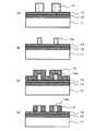
従来、ナノインプリント用テンプレートの製造方法としては、石英ガラス等の基板にエッチングを施し、基板の表面に凹凸のパターンを形成することによって行われる(例えば、特許文献1参照。)。図8は、従来のテンプレートの製造方法の一例を示す工程断面模式図である。 Conventionally, a method for manufacturing a template for nanoimprinting is performed by etching a substrate such as quartz glass and forming an uneven pattern on the surface of the substrate (see, for example, Patent Document 1). FIG. 8 is a process cross-sectional schematic diagram showing an example of a conventional template manufacturing method.
まず、図8(a)に示すように、テンプレートとなる石英ガラス等の基板81上に基板エッチング時のマスク材としてクロム(Cr)等の金属薄膜82を成膜し、その上に電子線レジストを塗布し、電子線(EB)リソグラフィ技術を用いて露光、現像等を行い、レジストパターン83を形成する。基板81に直接レジストパターンを形成する方法は、レジストの基板への密着性やレジストのエッチング耐性が不十分なため好ましくない。 First, as shown in FIG. 8A, a metal
次に、図8(b)に示すように、上記のレジストパターン83を酸素プラズマでスリミング処理を行い、レジストパターンの膜厚、幅をスリム化する。このスリミング工程は必須の工程ではなく、目標とするレジストパターン線幅に応じて実施するか否かを決めればよい。 Next, as shown in FIG. 8B, the
次に、図8(c)に示すように、スリミングしたレジストパターン83aをマスクとして金属薄膜82をエッチングし、金属薄膜パターン82aを形成する。次に、金属薄膜パターン82aをマスクとして基板81をエッチングし、図8(d)に示すように、凹部86を形成した基板81とする。次に、図8(e)に示すように、レジストパターン83aを剥離除去する。レジストパターン83aの除去は、基板81をエッチングする前であってもよい。 Next, as shown in FIG. 8C, the metal
次に、図8(f)に示すように、金属薄膜パターン82aをエッチングして除去し、基板81上に凹凸パターン87を設けたテンプレート80を作製する方法が用いられている。 Next, as shown in FIG. 8F, a method is used in which a metal
しかしながら、上記の従来のテンプレートの製造方法ではクロム等の金属薄膜のエッチングマスクに有機レジストを用いており、パターンの微細化に伴い解像力を上げるためにレジスト厚を薄くせざるを得ず、金属薄膜をエッチングして微細パターンを形成するときに、レジストのエッチング耐性の確保が難しいという問題があった。また、現状のEBリソグラフィ技術では安定して形成できる微細パターンの解像力に限界があり、例えば、ハーフピッチ22nm程度のパターンが解像限界であり、ハーフピッチ1Xnm(ハーフピッチ10nm以上20nm未満を意味する)クラスの微細パターン形成は困難であるという問題があった。また、パターンの微細化に伴い、テンプレートの電子線描画時間が非常に長くなるという問題があった。 However, in the above conventional template manufacturing method, an organic resist is used as an etching mask for a metal thin film such as chromium, and the resist thickness has to be reduced in order to increase resolution with the miniaturization of the pattern. When forming a fine pattern by etching, there is a problem that it is difficult to ensure the etching resistance of the resist. Further, there is a limit to the resolution of a fine pattern that can be stably formed with the current EB lithography technology. For example, a pattern with a half pitch of about 22 nm is the resolution limit, and means a half pitch of 1 × nm (half pitch of 10 nm or more and less than 20 nm). ) There was a problem that it was difficult to form a fine pattern of the class. In addition, with the miniaturization of the pattern, there is a problem that the electron beam drawing time of the template becomes very long.
そこで、本発明者はナノインプリント用テンプレートの製造方法において、金属薄膜のパターンエッチング時に、エッチングマスクのエッチング耐性を向上させ、かつ現状のEBリソグラフィ技術を用いてハーフピッチ1Xnmクラスの微細テンプレートの作製を可能にし、微細パターン描画においても描画時間の短縮が可能なテンプレートの製造方法を提案した。 Therefore, the present inventor can improve the etching resistance of the etching mask during the pattern etching of the metal thin film in the method of manufacturing the template for nanoimprint, and can produce a fine template of half pitch 1X nm class using the current EB lithography technology. In addition, a template manufacturing method capable of shortening the drawing time even in fine pattern drawing has been proposed.
図6及びそれに続く図7は、上記ナノインプリント用テンプレートの製造方法の一実施形態を示す工程断面図である。光透過性基板に凹凸のパターンを形成したナノインプリント用テンプレート60の製造方法である。図6及び図7に示されるように、光透過性基板61上に金属薄膜62を形成し、該金属薄膜62上に、レジストパターン63を形成する工程と、上記レジストパターンを酸素プラズマで処理してスリミングする工程と、スリミングしたレジストパターン63aの側面及び上面、並びに上記金属薄膜62の上面を覆うように被覆膜64を形成する工程と、上記の被覆膜64をエッチバックして、レジストパターン63a及び金属薄膜62を露出させるとともに、被覆膜をレジストパターン63aの側面に残して側壁マスク65とする工程と、レジストパターン63aを除去する工程と、側壁マスク65を用いて金属薄膜62をエッチングして金属薄膜パターン62aを形成する工程と、側壁マスク65を除去する工程と、金属薄膜パターン62aをマスクとして光透過性基板61をエッチングして凹凸のパターン67を形成する工程と、金属薄膜パターン62aを除去する工程と、を含むものである。 FIG. 6 and subsequent FIG. 7 are process cross-sectional views showing an embodiment of a method for producing the nanoimprint template. It is a manufacturing method of the
上記の製造方法は、金属薄膜のエッチングに側壁マスクを用いることで、金属薄膜エッチング時のマスクのエッチング耐性を向上させ、かつハーフピッチ1Xnm(10nm以上20nm未満)クラスの微細なテンプレートの作製を可能にし、また、電子線による微細パターン描画において、現状のハーフピッチ2Xnm(20nm以上30nm未満)クラスの描画時間で1Xnmクラスの側壁マスクが作製でき、描画時間の短縮を可能にするという利点を有するものである。 The above manufacturing method uses a sidewall mask to etch a metal thin film, thereby improving the etching resistance of the mask during the metal thin film etching and making a fine template of half pitch 1X nm (10 nm or more and less than 20 nm) class. In addition, in fine pattern drawing with an electron beam, a side mask of 1X nm class can be manufactured with a current half pitch 2X nm (20 nm or more and less than 30 nm) class drawing time, and the drawing time can be shortened. It is.
しかしながら、上記の製造方法において、レジストパターン63aの側面及び上面、並びに金属薄膜62の上面を覆うように被覆膜64を形成したときに、レジストパターン63a上にALD法で成膜された被覆膜64が斜めに成膜されて、傾き(テーパー)を生じてしまうことがあるという問題が生じていた。この現象は、特に金属薄膜にクロム系材料を用いた場合に顕著となる。被覆膜64が傾き(テーパー)を生じると、側壁マスクおよび金属薄膜パターンの寸法に大きな影響を生じ、目的とするテンプレートの凹凸のパターン寸法が得られなくなるという問題があった。 However, in the above manufacturing method, when the
本発明者は、上記の被覆膜が傾き(テーパー)を生じるという現象を種々検討し、被覆膜の傾き(テーパー)の原因が金属薄膜上のレジストパターンの断面形状によることを見出した。図5は、上記の現象の説明図であり、図5(c)は、上記ナノインプリント用テンプレートの製造方法の図6(c)と同じ工程図であり、スリミングしたレジストパターン63aの側面及び上面、並びに上記金属薄膜(Cr)62の上面を覆うように被覆膜(SiO2)64を形成した状態を示す。しかし、図5(c−1)に示すように、上記現象が生じた実際の試料の切断部の断面SEM写真を観察すると、金属薄膜(Cr)62上のレジストパターン63aの下部にすそ引きが見られ、図5(c−2)のレジストパターン63aの下部の断面模式図に示すように、レジストパターン63a下部に接する被覆膜(SiO2)64の底部付近が浮き上がっているのが観察される。The present inventor has studied various phenomena that the coating film is inclined (tapered), and found that the cause of the inclination (tapered) of the coating film is due to the cross-sectional shape of the resist pattern on the metal thin film. FIG. 5 is an explanatory diagram of the above phenomenon, and FIG. 5C is the same process diagram as FIG. 6C of the method for manufacturing the nanoimprint template, and the side and top surfaces of the
そこで、本発明は、上記の問題点に鑑みてなされたものである。すなわち、本発明の目的は、ナノインプリント用テンプレートの製造方法において、テンプレート基材となる光透過性基板上に設けた金属薄膜上にレジストパターンを形成するに際して、レジストパターンの側面に成膜された被覆膜に傾き(テーパー)が生じるのを抑制し、高精度の側壁マスク及び金属薄膜パターン寸法が安定して得られるナノインプリント用テンプレートの製造方法を提供することにある。 Therefore, the present invention has been made in view of the above problems. That is, an object of the present invention is to form a resist pattern on a side surface of a resist pattern when forming a resist pattern on a metal thin film provided on a light-transmitting substrate as a template base material in a method for producing a template for nanoimprinting. An object of the present invention is to provide a method for manufacturing a template for nanoimprinting that suppresses the occurrence of inclination (taper) in a covering film and stably obtains a highly accurate sidewall mask and metal thin film pattern dimensions.
上記の課題を解決するために、本発明の請求項1に係るナノインプリント用テンプレートの製造方法は、光透過性基板に凹凸のパターンを形成したナノインプリント用テンプレートの製造方法であって、光透過性基板上に金属薄膜およびシリコン含有膜がこの順に積層形成された基板の当該シリコン含有膜上に、レジストパターンを形成する工程と、前記レジストパターンの側面及び上面、並びに前記シリコン含有膜の上面を覆うように被覆膜を形成する工程と、前記被覆膜をエッチバックして、前記レジストパターン及び前記シリコン含有膜を露出させるとともに、前記被覆膜を前記レジストパターンの側面に残して側壁マスクとする工程と、前記レジストパターンを除去する工程と、前記側壁マスクを用いて前記シリコン含有膜および前記金属薄膜をこの順にエッチングしてシリコン含有膜パターンおよび金属薄膜パターンを形成する工程と、前記金属薄膜パターンをマスクとして、前記光透過性基板をエッチングして前記凹凸のパターンを形成する工程と、前記側壁マスク、前記シリコン含有膜パターンおよび前記金属薄膜パターンを除去する工程と、を含むことを特徴とするものである。 In order to solve the above problems, a method for producing a nanoimprint template according to
本発明の請求項2に係るナノインプリント用テンプレートの製造方法は、請求項1に記載のナノインプリント用テンプレートの製造方法において、前記被覆膜が、ALD法で形成されていることを特徴とするものである。 The method for producing a nanoimprint template according to
本発明の請求項3に係るナノインプリント用テンプレートの製造方法は、請求項1または請求項2に記載のナノインプリント用テンプレートの製造方法において、前記金属薄膜がクロムまたはクロムを含む化合物で形成されていることを特徴とするものである。 The method for producing a nanoimprint template according to claim 3 of the present invention is the method for producing a nanoimprint template according to
本発明の請求項4に係るナノインプリント用テンプレートの製造方法は、請求項1から請求項3までのうちのいずれか1項に記載のナノインプリント用テンプレートの製造方法において、前記レジストパターンを除去する工程が、酸素系のガスによるドライ処理により選択的に行われることを特徴とするものである。 The method for producing a nanoimprint template according to claim 4 of the present invention is the method for producing a nanoimprint template according to any one of
本発明の請求項5に係るナノインプリント用テンプレートの製造方法は、請求項1から請求項4までのうちのいずれか1項に記載のナノインプリント用テンプレートの製造方法において、前記光透過性基板をエッチングする前に、少なくとも前記側壁マスクを除去し、前記光透過性基板をエッチングして前記凹凸のパターンを形成する工程の後に、前記第1層目の金属薄膜パターンを除去することを特徴とするものである。 The method for producing a nanoimprint template according to claim 5 of the present invention is the method for producing a nanoimprint template according to any one of
本発明の請求項6に係るナノインプリント用テンプレートの製造方法は、請求項1から請求項5までのうちのいずれか1項に記載のナノインプリント用テンプレートの製造方法において、前記光透過性基板が、石英ガラス基板であることを特徴とするものである。 The method for producing a nanoimprint template according to claim 6 of the present invention is the method for producing a nanoimprint template according to any one of
本発明の請求項7に係るナノインプリント用テンプレートの製造方法は、請求項1から請求項4までのうちのいずれか1項に記載のナノインプリント用テンプレートの製造方法において、前記光透過性基板が石英ガラス基板であり、前記側壁マスクがシリコンを含む化合物より構成され、前記側壁マスクを除去する工程において前記側壁マスクが残存した場合には、前記光透過性基板をエッチングして前記凹凸のパターンを形成する工程で、前記残存した側壁マスクを除去することを特徴とするものである。 The method for producing a nanoimprint template according to claim 7 of the present invention is the method for producing a nanoimprint template according to any one of
本発明の請求項8に記載の発明に係るナノインプリント用テンプレートの製造方法は、光透過性基板に凹凸のパターンを形成したナノインプリント用テンプレートの製造方法であって、前記光透過性基板上に、2層以上の金属薄膜を形成する工程と、前記金属薄膜上に、レジストパターンを形成する工程と、前記レジストパターンを酸素プラズマで処理してスリミングする工程と、前記スリミングしたレジストパターンの側面及び上面、並びに前記金属薄膜の上面を覆うように被覆膜を形成する工程と、前記被覆膜をエッチバックして、前記レジストパターン及び前記金属薄膜を露出させるとともに、前記被覆膜を前記レジストパターンの側面に残して側壁マスクとする工程と、前記レジストパターンを除去する工程と、前記側壁マスクを用いて前記2層以上の金属薄膜を順にエッチングして金属薄膜パターンを形成する工程と、前記金属薄膜パターンをマスクとして、前記光透過性基板をエッチングして前記凹凸のパターンを形成する工程と、前記側壁マスクおよび前記2層以上の金属薄膜パターンを除去する工程と、を含むことを特徴とするものである。 A method for manufacturing a nanoimprint template according to an eighth aspect of the present invention is a method for manufacturing a nanoimprint template in which an uneven pattern is formed on a light transmissive substrate. A step of forming a metal thin film of a layer or more, a step of forming a resist pattern on the metal thin film, a step of slimming the resist pattern by treatment with oxygen plasma, a side surface and an upper surface of the slimmed resist pattern, And a step of forming a coating film so as to cover the upper surface of the metal thin film; and etching back the coating film to expose the resist pattern and the metal thin film, and the coating film is formed on the resist pattern. Using the sidewall mask as a sidewall mask, removing the resist pattern, and the sidewall mask; Etching the two or more layers of the metal thin film in order to form a metal thin film pattern, etching the light transmissive substrate using the metal thin film pattern as a mask, and forming the uneven pattern, And a step of removing the sidewall mask and the two or more metal thin film patterns.
本発明の請求項9に記載の発明に係るナノインプリント用テンプレートの製造方法は、請求項8に記載のナノインプリント用テンプレートの製造方法において、前記被覆膜が、ALD法で形成されていることを特徴とするものである。 The method for producing a nanoimprint template according to claim 9 of the present invention is the method for producing a nanoimprint template according to claim 8, wherein the coating film is formed by an ALD method. It is what.
本発明の請求項10に記載の発明に係るナノインプリント用テンプレートの製造方法は、請求項8または請求項9に記載のナノインプリント用テンプレートの製造方法において、前記2層以上の金属薄膜が、少なくとも前記光透過性基板に接する側の第1層目の金属薄膜と、前記第1層目の金属薄膜上に設けた第2層目の金属薄膜とで構成され、前記第1層目の金属薄膜がクロムまたはクロムを含む化合物で形成されていることを特徴とするものである。 The method for producing a nanoimprint template according to claim 10 of the present invention is the method for producing a nanoimprint template according to claim 8 or 9, wherein the two or more metal thin films are at least the light. A first layer metal thin film on the side in contact with the transparent substrate; and a second layer metal thin film provided on the first layer metal thin film, wherein the first layer metal thin film is chromium. Or it is formed with the compound containing chromium.
本発明の請求項11に記載の発明に係るナノインプリント用テンプレートの製造方法は、請求項8から請求項10までのうちのいずれか1項に記載のナノインプリント用テンプレートの製造方法において、前記レジストパターンを除去する工程が、酸素系のガスによるドライ処理により選択的に行われることを特徴とするものである。 The method for producing a nanoimprint template according to the invention described in
本発明の請求項12に記載の発明に係るナノインプリント用テンプレートの製造方法は、請求項8から請求項11までのうちのいずれか1項に記載のナノインプリント用テンプレートの製造方法において、前記側壁マスクおよび前記第2層目の金属薄膜パターンを除去する工程が、前記光透過性基板をエッチングする前であり、前記第1層目の金属薄膜パターンを除去する工程が、前記光透過性基板をエッチングして前記凹凸のパターンを形成する工程の後であることを特徴とするものである。 The nanoimprint template manufacturing method according to the invention described in
本発明の請求項13に記載の発明に係るナノインプリント用テンプレートの製造方法は、請求項8から請求項12までのうちのいずれか1項に記載のナノインプリント用テンプレートの製造方法において、前記光透過性基板が、石英ガラス基板であることを特徴とするものである。 The method for producing a nanoimprint template according to claim 13 of the present invention is the method for producing a nanoimprint template according to any one of claims 8 to 12, wherein the light-transmitting property is obtained. The substrate is a quartz glass substrate.
本発明の請求項14に記載の発明に係るナノインプリント用テンプレートの製造方法は、請求項8から請求項11までのうちのいずれか1項に記載のナノインプリント用テンプレートの製造方法において、前記光透過性基板が石英ガラス基板であり、前記側壁マスクがシリコンを含む化合物より構成され、前記側壁マスクを除去する工程において前記側壁マスクが残存した場合には、前記光透過性基板をエッチングして前記凹凸のパターンを形成する工程で、前記残存した側壁マスクを除去することを特徴とするものである。 The method for producing a nanoimprint template according to claim 14 of the present invention is the method for producing a nanoimprint template according to any one of claims 8 to 11, wherein the light-transmitting property is obtained. When the substrate is a quartz glass substrate, the sidewall mask is made of a compound containing silicon, and the sidewall mask remains in the step of removing the sidewall mask, the light transmissive substrate is etched to remove the unevenness. In the step of forming a pattern, the remaining sidewall mask is removed.
本発明のナノインプリント用テンプレートの製造方法によれば、光透過性基板上に設ける金属薄膜を2層以上の多層膜とすることにより、金属薄膜上のレジストパターンをすそ引きの抑制された高精度のパターンとして形成することができ、金属薄膜のエッチングに傾き(テーパー)のない側壁マスクを用い、金属薄膜エッチング時のマスクのエッチング耐性を向上させ、かつハーフピッチ1Xnm(10nm以上20nm未満)クラスの微細なテンプレートの作製が可能になる。また、電子線による微細パターン描画において、現状のハーフピッチ2Xnm(20nm以上30nm未満)クラスの描画時間で1Xnmクラスの側壁マスクが作製でき、描画時間の短縮が可能になるという効果を奏する。 According to the method for producing a template for nanoimprinting of the present invention, the metal thin film provided on the light-transmitting substrate is a multi-layered film of two or more layers. It can be formed as a pattern, uses a sidewall mask without inclination (taper) for etching a metal thin film, improves the etching resistance of the mask during metal thin film etching, and has a fine pitch of 1X nm (10 nm or more and less than 20 nm) class Template can be produced. In addition, in the fine pattern writing using an electron beam, a sidewall mask of 1X nm class can be manufactured with the current half pitch 2X nm (20 nm or more and less than 30 nm) class writing time, and the writing time can be shortened.
以下、図面に基づいて、本発明の実施形態に係るナノインプリント用テンプレートの製造方法について詳細に説明する。 Hereinafter, based on drawings, the manufacturing method of the template for nanoimprinting concerning the embodiment of the present invention is explained in detail.
(実施形態)
図1及びそれに続く図2は、本発明のナノインプリント用テンプレートの製造方法の一実施形態を示す工程断面図であり、光透過性基板上の金属薄膜が2層以上の多層膜で形成されている。以下の説明では、金属薄膜が2層膜の場合について例示するが、本発明の製造方法は2層に限定されず、金属薄膜を3層以上とすることも可能である。(Embodiment)
FIG. 1 and subsequent FIG. 2 are process cross-sectional views showing an embodiment of a method for producing a nanoimprint template of the present invention, in which a metal thin film on a light-transmitting substrate is formed of a multilayer film of two or more layers. . In the following description, the case where the metal thin film is a two-layer film will be exemplified, but the manufacturing method of the present invention is not limited to two layers, and the metal thin film can be three or more layers.
レジストパターンの断面形状や密着性などは、レジストパターンを形成する材料表面(下地)の影響を受ける。本発明の側壁マスクを用いた製造方法においては、レジストパターンの断面形状の矩形性、特にレジストパターンの底部にすそ引きがないことが重要な要素である。上記のように、光透過性基板上の金属薄膜を2層膜とすることで、レジストパターンと金属薄膜との最適な組み合わせを選択することが可能となる。また、使用する電子線レジストの選択の自由度を高めることができる。 The cross-sectional shape and adhesion of the resist pattern are affected by the material surface (underlying) that forms the resist pattern. In the manufacturing method using the side wall mask of the present invention, it is an important factor that the cross-sectional shape of the resist pattern is rectangular, and in particular, there is no skirting at the bottom of the resist pattern. As described above, an optimal combination of a resist pattern and a metal thin film can be selected by forming the metal thin film on the light-transmitting substrate as a two-layer film. Moreover, the freedom degree of selection of the electron beam resist to be used can be raised.
さらに、金属薄膜として例えばクロム系材料を用いた場合、クロム系材料よりなる金属薄膜をドライエッチングして微細パターンを形成するときに、通常、エッチングガスとして酸素を含む塩素ガスが用いられる。ハーフピッチ2Xnm(20nm以上30nm未満)以下の微細パターン加工では、微細パターンのエッチング速度が極端に小さくなるマイクロローディングの影響が顕著となり、エッチング時間が長くなり、金属薄膜のエッチングマスク材のエッチング耐性の確保が難しくなり、金属薄膜のドライエッチング中にマスク材が損傷してしまうという問題が生じることがある。そこで、本発明では金属薄膜を積層し、その好ましい形態として、光透過性基板に接する側の第1層目の金属薄膜はクロム系材料で形成し、その上にクロム系材料の金属薄膜の加工用に第2層目の金属薄膜を設け、レジストパターンを2層の金属薄膜パターンに順次変換し、第1層目のクロム系材料の金属薄膜パターンでテンプレートの微細パターン形成を行うものである。以下、図面を用いて説明する。 Further, when a chromium-based material is used as the metal thin film, for example, chlorine gas containing oxygen is usually used as an etching gas when the metal thin film made of the chromium-based material is dry-etched to form a fine pattern. In micropattern processing with a half pitch of 2X nm (20 nm or more and less than 30 nm) or less, the effect of microloading, in which the etching rate of the micropattern becomes extremely small, becomes significant, the etching time becomes long, and the etching resistance of the etching mask material of the metal thin film It may be difficult to ensure and the mask material may be damaged during dry etching of the metal thin film. Therefore, in the present invention, a metal thin film is laminated, and as a preferred form thereof, the metal thin film on the first layer on the side in contact with the light-transmitting substrate is formed of a chromium-based material, and the metal thin film of the chromium-based material is processed thereon. For this purpose, a metal thin film of the second layer is provided, the resist pattern is sequentially converted into a metal thin film pattern of two layers, and a fine pattern of the template is formed with the metal thin film pattern of the first layer of chromium-based material. Hereinafter, it demonstrates using drawing.
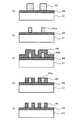
まず、図1(a)に示すように、テンプレートの材料となる光透過性基板11上に、第1層目の金属薄膜12、第2層目の金属薄膜13をスパッタリング法等の真空成膜方法で順に成膜して2層膜を形成した基板を準備する。次いで、この第2層目の金属薄膜13の上に、電子線描画によりレジストパターン14を形成する。 First, as shown in FIG. 1A, a first-layer metal
光透過性基板11としては、凹凸のパターンの位置精度を高精度に保持し、転写精度を得るために平滑性、平坦度が高く、テンプレート製造工程の洗浄などに用いる洗浄液への耐性に優れたものが好ましく、通常、合成石英ガラス基板等が用いられる。 As the light-transmitting
光透過性基板11に接する側の第1層目の金属薄膜12としては、石英ガラス基板等の光透過性基板11のエッチングガスとの選択比が十分にとれる耐エッチング性を有し、かつ第2層目の金属薄膜13のエッチングガスに耐性がある材料が好ましい。本発明において、第1層目の金属薄膜12としては、金属単体だけでなく、金属の酸化物、窒化物、酸窒化物等の金属化合物も含まれるものである。材料としては、例えば、クロム(Cr)、チタン(Ti)、タンタル(Ta)、アルミニウム(Al)等の金属、あるいは窒化クロム(CrN)、酸化クロム(CrO)、酸窒化クロム(CrNO)等のクロム系化合物、酸化タンタル(TaO)、酸窒化タンタル(TaNO)、酸化硼化タンタル(TaBO)、酸窒化硼化タンタル(TaBNO)等のタンタル系化合物、窒化チタン(TiN)等の金属化合物が、膜厚数nm〜10nm程度の範囲で用いられる。これらの材料の中で、特にクロム系材料は、石英ガラス基板のドライエッチングに用いるフッ素系ガスのプラズマに対して強い耐性をもち、またウェットエッチングが容易であり、フォトマスクの高品質・高精度のパターン形成材料としての使用実績があり、より好ましい材料である。 The first-layer metal
第2層目の金属薄膜13としては、第1層目の金属薄膜12をパターニングする時のマスクとなり、かつ第1層目の金属薄膜12のエッチングガスとの選択比がとれる材料を用いる。例えば、第2層目の金属薄膜13としては、シリコン系材料として、シリコン(Si)、または窒化シリコン(SiN)等のシリコンを含む化合物(シリコン含有膜)、あるいはタンタル系材料として、タンタル(Ta)、または窒化タンタル(TaN)、窒化硼化タンタル(TaBN)等のタンタルを含む化合物等が挙げられる。第2層目の金属薄膜13として上記材料(特にシリコン系材料)を用いることで、底部のすそ引きが抑制されたレジストパターン13aを形成することができる。第2層目の金属薄膜13の膜厚は、数nm〜10nm程度の範囲で用いるのが好ましい。 As the second-layer metal
次に、レジストパターン13を酸素プラズマで処理してスリミングし、図1(b)に示すように、スリミングしたレジストパターン14aを形成する。本発明において、スリミングとは、ウェットエッチングあるいはドライエッチング(酸素プラズマ処理を含む)等でパターン幅を細くし、パターン膜厚を薄くすることである。例えば、酸素プラズマ処理によるスリミングで最初に形成されたレジストパターンのピッチは変えずに、1/2程度のパターン幅、パターン膜厚とすることができる。なお、このスリミング工程は必須の工程ではない。 Next, the resist
次に、図1(c)に示すように、スリミングしたレジストパターン14aの側面及び上面、並びに第2層目の金属薄膜13の上面を覆うように被覆膜15を低温CVD(Chemical Vapor Deposition)法やALD(Atomic Layer Deposition)法等の低温真空成膜方法で形成する。レジストパターン14aは、被覆膜15形成におけるコア(芯材)となる。 Next, as shown in FIG. 1C, the
被覆膜15としては、レジストパターン14aに損傷を与えずに低温で成膜することができ、第2層目の金属薄膜13のエッチング時に、第2層目の金属薄膜13とのエッチング選択比がとれ耐エッチング性が大きい材料が好ましい。材料としては、例えば、酸化シリコン(SiO2)、窒化シリコン(SiN)、酸窒化シリコン(SiON)等のシリコン系、酸化アルミニウム(Al2O3)等のアルミニウム系、酸化ハフニウム(HfO)等のハフニウム系、窒化チタン(TiN)等のチタン系等の材料が挙げられる。被覆膜15の膜厚は、基本的には目標とするパターンのハーフピッチ設計分の膜厚が好ましく、数nm〜50nm程度の範囲で用いられる。被覆膜15を成膜するときの温度は、レジストパターン14aに損傷を与えない温度範囲であり、100℃以下が好ましく、室温程度がさらに好ましい。ALD法は、レジストパターンに損傷を与えずに均一な膜厚の被覆膜を、制御性良く低温で形成することができ、より好ましい成膜方法である。The
すなわち、ALD法を用いた場合においては、レジストパターン14aの側面への被覆膜15の堆積がCVD法を用いた場合より均一性が高く、レジストパターン14aの側面部、上面部へのより均一な被覆膜15の堆積が可能となる。そして、第2層目の金属薄膜13上にレジストパターン14aを形成することで、被覆膜15形成における芯材としてのレジストパターン14aを、底部のすそ引きが抑制された形状にすることができる。そのため、2層の金属薄膜のうちの第2層目の金属薄膜13上にレジストパターン14aを形成し、かつALD法を用いて被覆膜15を形成することで、後述する側壁マスクの形成において、側壁マスクをより垂直形状に形成することが可能となる。さらに、芯材に有機レジストを用いた場合において、低温成膜が可能なためレジストパターン14aの形状を損傷せず、レジストパターン形状を保ち易く側壁マスク形状が良好となる。CVD法では低温での均一な成膜は難しいが、ALD法では室温成膜も可能となる。 That is, in the case of using the ALD method, the deposition of the
上記のようにALD法を用いると、側壁マスクのパターンがより垂直形状になるため、特に、側壁マスクがエッチングマスクとなってパターン転写されるプロセス(以後、側壁プロセスとも言う)においては、微細なパターンの寸法制御性が格段に向上する。それにより半導体基板などへの転写原版の型となるテンプレートを高精度で作製することが可能となる。 When the ALD method is used as described above, the pattern of the sidewall mask becomes more vertical, and therefore, in the process of pattern transfer using the sidewall mask as an etching mask (hereinafter also referred to as a sidewall process), it is fine. The dimensional controllability of the pattern is greatly improved. As a result, it becomes possible to manufacture a template that becomes a mold of a transfer master on a semiconductor substrate or the like with high accuracy.
ここで、本発明の被覆膜15形成におけるにおけるALD法とCVD法の相違点について、さらに詳しく述べる。
後述する側壁マスクを用いた本発明のテンプレートの製造プロセスでは、被覆膜15の成膜厚みのばらつきがそのままパターンCD(Critical Dimension:重要な寸法)ばらつきに直結するため、被覆膜15の成膜厚みの均一性、特にレジストパターン14aの側面の被覆膜の均一性が重要となる。ALD法は飽和表面反応を利用した原子層成膜方法なので、原子層を1層ごとに成膜することが可能である。ALD法による成膜量は、およそ0.1nm〜0.2nm/cycle程度である。Here, the difference between the ALD method and the CVD method in forming the
In the template manufacturing process of the present invention using the side wall mask, which will be described later, the variation in the thickness of the
一方、CVD法では表面反応が次々と進行するため膜厚制御性がALD法に比べて劣り、CVD法は基本的に成膜時間制御なので装置コンディションで成膜速度が変化すると側壁の被覆膜の均一性が損なわれる。特に膜厚が小さい場合には、膜厚分布と膜厚中心値のずれが生ずる。また、CVD法ではカバレッジ性(形状追随性)もALD法に比べて劣り、特にパターン側壁部に著しい。CVD法は凸部上方ほど成膜されやすく、凹部には成膜されにくいという特性があり、通常CVD法はその点を成膜条件で調整するのだが、原理的にALD法の方が有利である。 On the other hand, since the surface reaction progresses one after another in the CVD method, the film thickness controllability is inferior to that of the ALD method, and the CVD method is basically a film formation time control. The uniformity of is impaired. In particular, when the film thickness is small, a deviation between the film thickness distribution and the film thickness center value occurs. Further, the CVD method is inferior to the ALD method in coverage (shape followability), and is particularly remarkable in the pattern side wall. The CVD method has a characteristic that it is easy to form a film at the upper part of the convex part and is difficult to form a film in the concave part. Usually, the CVD method adjusts the point according to the film forming condition, but the ALD method is more advantageous in principle. is there.
被覆膜15の成膜時に、芯材としてレジスト以外の材料、例えば無機化合物を用いた場合、芯材形成(パターニング)工程において芯材がオーバーエッチングされると、芯材の下層の第2層目の金属薄膜13にダメージが入り、CDシフトの原因となる。レジストの芯材であれば、レジストパターン形成時に第2層目の金属薄膜13へのダメージがないため、より好ましい。また後述するように、芯材がレジストであれば、弱いアッシング条件を用いることで、側壁マスクへのダメージを最小限に抑えて芯材を除去することが可能となる。
上記のように、微細パターンを有するテンプレートの製造においては芯材にレジストを用いるのが望ましく、レジストの芯材で側壁プロセスを実施するためには、ALD法による被覆膜の低温成膜がより好ましい。以下、図面に基づいて説明を続ける。When a material other than a resist, such as an inorganic compound, is used as the core material when forming the
As described above, in the manufacture of a template having a fine pattern, it is desirable to use a resist as a core material. In order to perform a side wall process with a resist core material, it is more necessary to form a coating film at a low temperature by the ALD method. preferable. Hereinafter, description will be continued based on the drawings.
次に、被覆膜15をエッチバックして、図1(d)に示すように、レジストパターン14a及び第2層目の金属薄膜13を露出させるとともに、被覆膜15をレジストパターン14aの側面に残して側壁マスク16とする。本発明において、側壁マスク16は、コア(核、芯材)となるレジストパターン13aよりなるダミーパターンの側壁に被覆膜で側壁パターンを形成し、この側壁パターンをエッチングマスクとして用いるマスクを意味するものであり、ダミーパターンのピッチの半分のピッチでラインアンドスペースパターンを形成することが可能となる。 Next, the
エッチバックは、被覆膜15の材料に応じて適切なエッチングガスを用いて行われる。例えば、被覆膜15が酸化シリコン(SiO2)で形成されている場合には、フッ素系のCF4、CHF3、C2F6等のガス、あるいはこれらの混合ガスがエッチングガスとして用いられる。The etch back is performed using an appropriate etching gas according to the material of the
次に、レジストパターン14aを除去し、図2(e)に示すように、第2層目の金属薄膜13上に側壁マスク16を形成した光透過性基板11とする。本発明においては、被覆膜15をエッチバックし、レジストパターン14aの上部表面を露出させているので、レジストパターン14aの除去は容易にできる。 Next, the resist
さらに、本発明においては、側壁マスク16を形成するときにコアとなる材料が有機レジストなので、レジストパターン14aの除去は酸素系のガスを用いてドライ処理により選択的に除去することができる。例えば、酸素プラズマによるドライエッチングあるいはオゾン処理等のドライ処理が挙げられる。従来のコアとなる材料に無機化合物を用いてウェットエッチング処理する方法では、コア材料の除去時に、ウェットエッチングで生じるエッチング液の表面張力による側面マスクのパターンの倒壊や変形が生じるおそれがあり、ドライエッチングで処理する方法であったとしても、コア材料のエッチングガスによって側壁マスクにダメージが蓄積し、パターンの倒壊や変形が生じるおそれがあった。しかしながら、本発明のコア材料のレジストパターン14aの除去にドライ処理を用いる方法により、側面マスク16のパターンの倒壊や変形が防止できるという効果が得られる。コア材料に有機レジストを用いる本発明の方法は、レジストにエッチング耐性を必要としないので、レジストのパターン寸法やパターンエッジのラフネスの制御性が良く、コア材料に無機化合物を用いる方法に比べ、コア材料の加工工程が少なくてすみ、高品質な側壁マスクを得ることが可能である。 Furthermore, in the present invention, since the material that becomes the core when forming the
本実施形態においては、第1層目の金属薄膜12にクロム系材料を用いた場合、第2層目の金属薄膜13材料にシリコン系材料、側壁マスク16にも同じシリコン系材料を用いることで、第2層目の金属薄膜13と側壁マスク16との密着性を意図的に上げることが可能となる。密着性を上げることにより、第1層目の金属薄膜12のエッチング加工前に光透過性基板11に付着したパーティクル等を除去するための洗浄を強い条件で行うことが可能となり、テンプレートの製造工程の途中で欠陥の発生原因となるパーティクル等を十分に洗浄して除去し、テンプレートの欠陥を低減することが可能となる。側壁マスク16の除去は、第1層目の金属薄膜12のパターン形成後、または光透過性基板11をエッチングし、第1層目の金属薄膜12のパターンを除去するときに、リフトオフ法で除去することができる。 In this embodiment, when a chromium-based material is used for the first-layer metal
次に、図2(f)に示すように、側壁マスク16を用いて第2層目の金属薄膜13をエッチングして金属薄膜パターン13aを形成し、次いで、第2層目の金属薄膜パターン13aをエッチングマスクにして第1層目の金属薄膜12をエッチングして、第1層目の金属薄膜パターン12aを形成する。 Next, as shown in FIG. 2F, the second-layer metal
例えば、光透過性基板11に石英ガラス、側壁マスク16に酸化シリコン(SiO2)を用い、第1層目の金属薄膜12がクロムまたはクロムを含む化合物であり、第2層目の金属薄膜パターン13aがシリコン系材料の場合には、エッチングガスとして酸素と塩素との混合ガスを用いて第1層目の金属薄膜12をドライエッチングすることにより、エッチング選択比が大きくとれ、側壁マスク16及び光透過性基板11への損傷を抑制しつつ、第1層目の金属薄膜パターン12aを形成することができる。For example, quartz glass is used for the light-transmitting
次に、第1層目の金属薄膜パターン12aをエッチングマスクにして光透過性基板11をエッチングし、図2(g)に示すように、光透過性基板11に凹部17を形成する。例えば、光透過性基板11が石英ガラスであるときには、第1層目の金属薄膜パターン12aの材料にクロムまたはクロムを含む化合物を用い、光透過性基板11をフッ素系ガスでドライエッチングすることにより、エッチング選択比が大きくとれ、光透過性基板11に凹凸のパターンを形成することができる。 Next, the
次に、側壁マスク16、第2層目の金属薄膜パターン13a及び第1層目の金属薄膜パターン12aを除去し、図2(h)に示すように、光透過性基板11に凹凸パターン18を形成したナノインプリント用テンプレート10が得られる。 Next, the
側壁マスク16の除去方法としては、側壁マスク16に用いた被覆膜15の材料の特性及び第2層目の金属薄膜パターン13aとの密着性等により異なるが、ウェットエッチング、ドライエッチング、液体による洗浄等の中から最適な方法を用いることができる。 The method for removing the
例えば、側壁マスク16と第2層目の金属薄膜パターン13aとの密着性が低い場合には、水を用いたウェット洗浄で酸化シリコンよりなる側壁マスク16を除去することができ、製造工程が簡易化できる利点がある。ウェット洗浄に用いる水としては、例えば、純水、オゾン水、テンプレートに影響を与えない機能水等が挙げられる。使用する水は、テンプレートに損傷等の影響を与えない範囲において、加温してもよい。また、金属薄膜パターンや光透過性基板に損傷等の影響を与えない範囲において、超音波等の物理洗浄を付加してもよい。 For example, when the adhesion between the
さらに、本発明においては、光透過性基板11が石英ガラス基板であり、側壁マスク16が酸化シリコン等のシリコンを含む化合物より構成され、上記の側壁マスク16を除去する工程において、もしも側壁マスク16が残存した場合には、下記の光透過性基板11をドライエッチングして凹凸のパターンを形成する工程で、残存した側壁マスク16を同時に除去することが可能となり、テンプレート製造工程がより容易になるという利点がある。 Further, in the present invention, if the
第1層目の金属薄膜パターン12aの除去は、ウェットエッチング、ドライエッチングのいずれかの方法が用いられる。例えば、第1層目の金属薄膜パターン12aがクロム(Cr)またはクロムを含む化合物の場合には、硝酸第2セリウムアンモニウム水溶液によるウェットエッチングで容易に除去することができる。 To remove the first-layer metal
(他の実施形態)
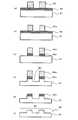
上記の工程において、側壁マスク16及び第2層目の金属薄膜パターン13aの除去は、光透過性基板11をエッチングする前であってもよい。図3に光透過性基板11のエッチング前に、側壁マスク16及び第2層目の金属薄膜パターン13aを除去する工程の実施形態の一例を示す。図3は、図1と同じ符号を用いており、製造工程の前半は図1の図1(a)〜図1(d)と同じであるので省略する。(Other embodiments)
In the above step, the removal of the
図3に示すように、第2層目の金属薄膜13上に側壁マスク16を形成する(図3(e))。次に、側壁マスク16を用いて第2層目の金属薄膜13をエッチングして金属薄膜パターン13aを形成し(図3(f))、次いで、第2層目の金属薄膜パターン13aをエッチングマスクにして第1層目の金属薄膜12をエッチングして、第1層目の金属薄膜パターン12aを形成する(図3(g))。 As shown in FIG. 3, a
側壁マスク16の除去は、第2層目の金属薄膜パターン13aの形成後で、第1層目の金属薄膜パターン12aの形成前であってもよいし、第1層目の金属薄膜パターン12aの形成後であってもよい。 The removal of the
第1層目の金属薄膜パターン12aの形成後、第2層目の金属薄膜パターン13aを除去し(図3(h))、第1層目の金属薄膜パターン12aをマスクにして光透過性基板11をドライエッチングし、光透過性基板11に凹部17を形成する(図3(i))。 After the formation of the first metal
次いで、第1層目の金属薄膜パターン12aを除去し、光透過性基板11に凹凸パターン18を形成したナノインプリント用テンプレート10を得る(図3(j))。 Next, the metal
本実施形態のナノインプリント用テンプレートの製造方法は、光透過性基板上に設ける金属薄膜を2層膜とし、第1層目の金属薄膜は、光透過性基板とのエッチング選択比が十分にとれる耐エッチング性を有し、かつ第2層目の金属薄膜のエッチングガスに耐性がある材料を用い、第2層目の金属薄膜上のレジストパターンをすそ引きのない高精度のパターンとし、断面形状が傾き(テーパー)にない矩形状の側壁マスクの安定的な形成を可能とし、ハーフピッチ1Xnm(10nm以上20nm未満)クラスの微細な金属薄膜パターンの形成が可能になる。側壁マスクと2層の金属薄膜パターンを用いることにより、現状のEBリソグラフィ技術では困難とされているハーフピッチ1Xnmクラスの微細パターンの形成が可能となる。また、側壁マスクを用いることで、ハーフピッチ2Xnm(20nm以上30nm未満)クラスの描画時間で1Xnmクラスの側壁マスクを作製することができ、描画時間の短縮が可能になる。
次に、実施例により本発明を説明する。In the manufacturing method of the template for nanoimprinting according to the present embodiment, the metal thin film provided on the light transmissive substrate is a two-layer film, and the first metal thin film has a resistance to etching which allows a sufficient etching selectivity with respect to the light transmissive substrate. Using a material that is etchable and resistant to the etching gas of the second layer metal thin film, the resist pattern on the second layer metal thin film is made into a highly accurate pattern without striking, and the cross-sectional shape is A rectangular sidewall mask having no inclination (taper) can be stably formed, and a fine metal thin film pattern having a half pitch of 1 × nm (10 nm or more and less than 20 nm) can be formed. By using the sidewall mask and the two-layer metal thin film pattern, it is possible to form a fine pattern of half pitch 1X nm class, which is considered difficult with the current EB lithography technology. In addition, by using the sidewall mask, a sidewall mask of 1X nm class can be manufactured with a half pitch 2X nm (20 nm or more and less than 30 nm) class drawing time, and the writing time can be shortened.
Next, an example explains the present invention.
(実施例1)
図1(a)に示すように、テンプレート用の光透過性基板11として、外形が6インチ角、厚さ0.25インチの合成石英ガラス基板を用い、基板の一方の主面上に、スパッタリング法でクロム(Cr)を膜厚5nm成膜して第1層目の金属薄膜12としてCr膜を形成し、次に窒化タンタル(TaN)膜を膜厚5nm成膜して第2層目の金属薄膜13を形成した基板を準備した。次いで、この第2層目のTaN膜上にポジ型電子線レジストZEP−520(日本ゼオン社製)を塗布し、電子線描画によりパターン幅30nm、ハーフピッチ30nmのラインアンドスペースよりなるレジスト厚60nmのレジストパターン14を形成した。TaN膜上のレジストパターンは、パターンの下部のすそ引きが従来よりも抑制された、断面形状がほぼ矩形形状のレジストパターンであった。Example 1
As shown in FIG. 1A, a synthetic quartz glass substrate having an outer shape of 6 inches square and a thickness of 0.25 inches is used as the
次に、レジストパターンを酸素プラズマでドライエッチングしてスリミングし、図1(b)に示すように、パターン幅15nmのスリミングしたレジストパターン14aを形成した。スリミングしたレジストパターン14aもパターンの下部のすそ引きが従来よりも抑制された、断面がほぼ矩形形状のレジストパターンであった。 Next, the resist pattern was slimmed by dry etching with oxygen plasma to form a slimmed resist
次に、スリミングしたレジストパターンの側面及び上面、並びにTaN膜の上面を覆うようにALD法により酸化シリコン(SiO2)を成膜し、図1(c)に示すように、厚さ15nmのSiO2の被覆膜15を形成した。Next, silicon oxide (SiO2 ) is formed by ALD so as to cover the side surface and upper surface of the slimmed resist pattern and the upper surface of the TaN film, and as shown in FIG.Two coating
次に、CF4ガスを用いてSiO2の被覆膜全面をドライエッチングによりエッチバックし、図1(d)に示すように、レジストパターン14a及び第2層目の金属薄膜(TaN膜)13を露出させるとともに、SiO2の被覆膜をレジストパターンの側面に残して側壁マスク16を形成した。Next, the entire surface of the SiO2 coating film is etched back by dry etching using CF4 gas, and as shown in FIG. 1D, a resist
次に、酸素プラズマによる弱いドライエッチングで選択的にレジストパターンを除去し、図3(e)に示すように、Cr膜とTaN膜の2層金属薄膜上にSiO2の側壁マスク16を形成した基板を作成した。本実施例においては、コア材料が有機レジストなので、レジストパターンの除去は容易であり、側面マスクの倒れや変形は生じなかった。SiO2の側壁マスクは、パターン幅15nm、厚さ45nm、ハーフピッチ15nmのラインアンドスペースで、電子線描画時の1/2のパターン幅、ハーフピッチとなった。Next, the resist pattern was selectively removed by weak dry etching with oxygen plasma, and as shown in FIG. 3E, a SiO2 sidewall mask 16 was formed on the two-layer metal thin film of the Cr film and the TaN film. A substrate was created. In the present embodiment, since the core material is an organic resist, the resist pattern can be easily removed, and the side mask has not collapsed or deformed. The SiO2 side wall mask had a line width of 15 nm, a thickness of 45 nm, and a half pitch of 15 nm, and had a pattern width and a half pitch of ½ at the time of electron beam drawing.
次に、図3(f)に示すように、SiO2の側壁マスク16を用いて第2層目のTaN膜を塩素ガスでドライエッチングし、TaN膜パターンを形成した。このとき、マスクとしたSiO2、および下層のCr膜はいずれも塩素ガスに耐性があるので、損傷は生じなかった。Next, as shown in FIG. 3F, the TaN film of the second layer was dry-etched with chlorine gas using the SiO2 sidewall mask 16 to form a TaN film pattern. At this time, both the SiO2 used as a mask and the underlying Cr film were resistant to chlorine gas, and thus were not damaged.
次に、CF4ガスを用いてSiO2の側壁マスクをドライエッチングして除去した。Next, the sidewall mask of SiO2 was removed by dry etching using CF4 gas.
次に、図3(g)に示すように、第2層目の金属薄膜(TaN膜)パターン13aをマスクにして塩素と酸素の混合ガスを用いて第1層目のCr膜をドライエッチングし、第1層目の金属薄膜(Cr膜)パターン12aを形成した。TaN膜パターンは塩素と酸素の混合ガスに耐性があるので損傷は生じなかった。 Next, as shown in FIG. 3G, the first-layer Cr film is dry-etched using a mixed gas of chlorine and oxygen using the second-layer metal thin film (TaN film)
次に、図3(h)に示すように、塩素ガスを用いてTaN膜パターンをドライエッチングして除去した。Cr膜パターンは塩素ガスに耐性があるので損傷は生じなかった。 Next, as shown in FIG. 3H, the TaN film pattern was removed by dry etching using chlorine gas. Since the Cr film pattern was resistant to chlorine gas, no damage occurred.
次に、図3(i)に示すように、Cr膜パターンをエッチングマスクにしてCF4ガスを用いて石英ガラス基板をドライエッチングし、石英ガラス基板に凹部を形成した。Next, as shown in FIG. 3 (i), the quartz glass substrate was dry-etched using CF4 gas with the Cr film pattern as an etching mask to form a recess in the quartz glass substrate.
次に、Cr膜パターンを硝酸第2セリウムアンモニウム水溶液によるウェットエッチングで除去し、図3(j)に示すように、石英ガラス基板に、パターン幅15nm、ハーフピッチ15nmのラインアンドスペースの凹凸パターン18を形成したナノインプリント用テンプレート10を作製した。 Next, the Cr film pattern is removed by wet etching with a ceric ammonium nitrate aqueous solution, and as shown in FIG. 3 (j), a line-and-space
(実施例2)
図1(a)に示すように、テンプレート用の光透過性基板11として、実施例1と同様に、外形が6インチ角、厚さ0.25インチの合成石英ガラス基板を用い、基板の一方の主面上に、スパッタリング法で窒化クロム(CrN)を膜厚5nm成膜して第1層目の金属薄膜12としてCrN膜を形成し、次に酸化シリコン(SiO2)を膜厚5nm成膜して第2層目の金属薄膜13を形成した基板を準備した。次いで、この第2層目のSiO2膜上にポジ型電子線レジストZEP−520(日本ゼオン社製)を塗布し、電子線描画によりパターン幅30nm、ハーフピッチ30nmのラインアンドスペースよりなるレジスト厚60nmのレジストパターン14を形成した。SiO2膜上のレジストパターンは、パターンの下部のすそ引きが従来よりも抑制された、断面形状がほぼ矩形形状のレジストパターンであった。(Example 2)
As shown in FIG. 1A, a synthetic quartz glass substrate having an outer shape of 6 inches square and a thickness of 0.25 inches is used as the
次に、レジストパターンを酸素プラズマでドライエッチングしてスリミングし、図1(b)に示すように、パターン幅15nmのスリミングしたレジストパターン14aを形成した。スリミングしたレジストパターン14aもパターンの下部のすそ引きが従来よりも抑制された、断面がほぼ矩形形状のレジストパターンであった。 Next, the resist pattern was slimmed by dry etching with oxygen plasma to form a slimmed resist
次に、スリミングしたレジストパターン14aの側面及び上面、並びにSiO2膜の上面を覆うように、ALD法により酸化シリコン(SiO2)を成膜し、図1(c)に示すように、厚さ15nmのSiO2の被覆膜15を形成した。Next, silicon oxide (SiO2 ) is formed by an ALD method so as to cover the side surface and upper surface of the slimmed resist
次に、図1(d)に示すように、CF4ガスを用いてSiO2の被覆膜全面をドライエッチングによりエッチバックし、レジストパターン14aを露出させるとともに、SiO2の被覆膜をレジストパターンの側面に残してSiO2の側壁マスク16を形成した。エッチバックのとき、第2層目の金属薄膜SiO2も多少エッチングされるが、問題は生じなかった。Next, as shown in FIG. 1D, the entire SiO2 coating film is etched back by dry etching using CF4 gas to expose the resist
次に、図4(e)に示すように、酸素プラズマによる弱いドライエッチングで選択的にレジストパターンを除去し、CrN膜とSiO2膜の2層金属薄膜上にSiO2の側壁マスク16を形成した基板を作成した。本実施例においては、コア材料が有機レジストなので、レジストパターンの除去は容易であり、第2層目の金属薄膜SiO2と側壁マスクSiO2とは密着性が良好で、側壁マスクの倒れや変形は生じなかった。SiO2の側壁マスクは、パターン幅15nm、厚さ45nm、ハーフピッチ15nmのラインアンドスペースであった。Next, as shown in FIG. 4 (e), to remove selectively the resist pattern by a weak dry etching with oxygen plasma, forming a
次に、第1層目の金属薄膜CrN膜をエッチング停止層として用いて、露出している第2層目金属薄膜(SiO2膜)13をCF4ガスでドライエッチングし、図4(f)に示すように、第2層目の金属薄膜(SiO2膜)パターン13aを形成した。このとき、第2層目SiO2膜と側壁マスクSiO2膜とではエッチング選択比が取れないので、側壁マスクSiO2膜も膜減りするが、側壁マスクSiO2膜は十分な厚さがあるため、第2層目SiO2膜のパターン形成には支障はなかった。Next, the exposed second-layer metal thin film (SiO2 film) 13 is dry-etched with CF4 gas using the first-layer metal thin film CrN film as an etching stop layer, and FIG. As shown in FIG. 2, a second-layer metal thin film (SiO2 film)
続いて、側壁マスクSiO2膜及び第2層目のSiO2膜パターンをマスクにして塩素と酸素の混合ガスを用いて第1層目のCrN膜をドライエッチングし、CrN膜パターンを形成した。側壁マスクSiO2膜及び第2層目のSiO2膜パターンは、塩素と酸素の混合ガスに耐性があるので損傷は生じなかった。Subsequently, the first layer CrN film was dry-etched using a mixed gas of chlorine and oxygen using the sidewall mask SiO2 film and the second layer SiO2 film pattern as a mask to form a CrN film pattern. The sidewall mask SiO2 film and the second-layer SiO2 film pattern were resistant to a mixed gas of chlorine and oxygen, and thus were not damaged.
次に、CrN膜パターンをエッチングマスクにしてCF4ガスを用いて石英ガラス基板をドライエッチングし、図4(g)に示すように、石英ガラス基板に凹部17を形成した。石英ガラス基板のエッチング時に、CrN膜パターン上の第2層目のSiO2膜パターン及び側壁マスクSiO2膜もエッチング除去された。Next, the quartz glass substrate was dry-etched using CF4 gas using the CrN film pattern as an etching mask to form a
次に、CrNパターンを硝酸第2セリウムアンモニウム水溶液によるウェットエッチングで除去し、図4(h)に示すように、石英ガラス基板に、パターン幅15nm、ハーフピッチ15nmのラインアンドスペースの凹凸パターン18を形成したナノインプリント用テンプレート10を作製した。 Next, the CrN pattern is removed by wet etching with an aqueous solution of ceric ammonium nitrate, and a line-and-space
(実施例3)
図1(a)に示すように、テンプレート用の光透過性基板11として、実施例1と同様に、外形が6インチ角、厚さ0.25インチの合成石英ガラス基板を用い、基板の一方の主面上に、スパッタリング法でクロム(Cr)を膜厚5nm成膜して第1層目の金属薄膜12としてCr膜を形成し、次にシリコン(Si)を膜厚5nm成膜して第2層目の金属薄膜(シリコン含有膜)13を形成した基板を準備した。次いで、この第2層目のSi膜上にポジ型電子線レジストZEP−520(日本ゼオン社製)を塗布し、電子線描画によりパターン幅30nm、ハーフピッチ30nmのラインアンドスペースよりなるレジスト厚60nmのレジストパターン14を形成した。Si膜上のレジストパターンは、パターンの下部のすそ引きが従来よりも抑制された、断面形状がほぼ矩形形状のレジストパターンであった。(Example 3)
As shown in FIG. 1A, a synthetic quartz glass substrate having an outer shape of 6 inches square and a thickness of 0.25 inches is used as the
次に、レジストパターンを酸素プラズマでドライエッチングしてスリミングし、図1(b)に示すように、パターン幅15nmのスリミングしたレジストパターン14aを形成した。スリミングしたレジストパターン14aもパターンの下部のすそ引きが従来よりも抑制された、断面がほぼ矩形形状のレジストパターンであった。 Next, the resist pattern was slimmed by dry etching with oxygen plasma to form a slimmed resist
次に、スリミングしたレジストパターン14aの側面及び上面、並びにSi膜の上面を覆うように、ALD法により酸化シリコン(SiO2)を成膜し、図1(c)に示すように、厚さ15nmのSiO2の被覆膜15を形成した。Next, silicon oxide (SiO2 ) is formed by ALD so as to cover the side and upper surfaces of the slimmed resist
次に、図1(d)に示すように、CF4ガスを用いてSiO2の被覆膜全面をドライエッチングによりエッチバックし、レジストパターン14aを露出させるとともに、SiO2の被覆膜をレジストパターンの側面に残してSiO2の側壁マスク16を形成した。エッチバックのとき、第2層目の金属薄膜(シリコン含有膜)Siもエッチングされるが、問題は生じなかった。Next, as shown in FIG. 1D, the entire SiO2 coating film is etched back by dry etching using CF4 gas to expose the resist
次に、図4(e)に示すように、酸素プラズマによるドライエッチングで選択的にレジストパターンを除去し、Cr膜とSi膜の2層金属薄膜上にSiO2の側壁マスク16を形成した基板を作成した。本実施例においては、コア材料が有機レジストなので、レジストパターンの除去は容易であり、側壁マスクの倒れや変形は生じなかった。SiO2の側壁マスクは、パターン幅15nm、厚さ45nm、ハーフピッチ15nmのラインアンドスペースであった。Next, as shown in FIG. 4E, the resist pattern is selectively removed by dry etching using oxygen plasma, and a SiO2 sidewall mask 16 is formed on the two-layer metal thin film of the Cr film and the Si film. It was created. In this embodiment, since the core material is an organic resist, the resist pattern can be easily removed, and the side wall mask does not collapse or deform. The sidewall mask of SiO2 was a line and space pattern having a pattern width of 15 nm, a thickness of 45 nm, and a half pitch of 15 nm.
次に、第1層目の金属薄膜Cr膜をエッチング停止層として用いて、露出している第2層目金属薄膜(シリコン含有膜、Si膜)13をCF4ガスでドライエッチングし、図4(f)に示すように、第2層目の金属薄膜(シリコン含有膜、Si膜)パターン13aを形成した。このとき、第2層目Si膜と側壁マスクSiO2膜とのエッチング選択比により、側壁マスクSiO2膜も膜減りするが、側壁マスクSiO2膜は十分な厚さがあるため、第2層目Si膜のパターン形成には支障はなかった。Next, the exposed second-layer metal thin film (silicon-containing film, Si film) 13 is dry-etched with CF4 gas using the first-layer metal thin film Cr film as an etching stop layer, and FIG. As shown in (f), a second-layer metal thin film (silicon-containing film, Si film)
続いて、側壁マスクSiO2膜及び第2層目のSi膜パターンをマスクにして塩素と酸素の混合ガスを用いて第1層目のCr膜をドライエッチングし、Cr膜パターンを形成した。Subsequently, the first layer Cr film was dry-etched using a mixed gas of chlorine and oxygen using the sidewall mask SiO2 film and the second layer Si film pattern as a mask to form a Cr film pattern.
次に、Cr膜パターンをエッチングマスクにしてCF4ガスを用いて石英ガラス基板をドライエッチングし、図4(g)に示すように、石英ガラス基板に凹部17を形成した。石英ガラス基板のエッチング時に、Cr膜パターン上の第2層目のSi膜パターン及び側壁マスクSiO2膜もエッチング除去された。Next, the quartz glass substrate was dry-etched using CF4 gas with the Cr film pattern as an etching mask to form a
次に、Crパターンを硝酸第2セリウムアンモニウム水溶液によるウェットエッチングで除去し、図4(h)に示すように、石英ガラス基板に、パターン幅15nm、ハーフピッチ15nmのラインアンドスペースの凹凸パターン18を形成したナノインプリント用テンプレート10を作製した。 Next, the Cr pattern was removed by wet etching with a ceric ammonium nitrate aqueous solution, and a line-and-
10 テンプレート
11 光透過性基板
12 第1層目の金属薄膜
12a 第1層目の金属薄膜パターン
13 第2層目の金属薄膜
13a 第2層目の金属薄膜パターン
14、14a レジストパターン
15 被覆膜
16 側壁マスク
17 凹部
18 凹凸パターン
60 テンプレート
61 光透過性基板
62 金属薄膜
62a 金属薄膜パターン
63、63a レジストパターン
64 被覆膜
65 側壁マスク
66 凹部
67 凹凸パターン
80 テンプレート
81 光透過性基板
82 金属薄膜
82a 金属薄膜パターン
83、83a レジストパターン
86 凹部
87 凹凸パターンDESCRIPTION OF
Claims (14)
Translated fromJapanese光透過性基板上に金属薄膜およびシリコン含有膜がこの順に積層形成された基板の当該シリコン含有膜上に、レジストパターンを形成する工程と、
前記レジストパターンの側面及び上面、並びに前記シリコン含有膜の上面を覆うように被覆膜を形成する工程と、
前記被覆膜をエッチバックして、前記レジストパターン及び前記シリコン含有膜を露出させるとともに、前記被覆膜を前記レジストパターンの側面に残して側壁マスクとする工程と、
前記レジストパターンを除去する工程と、
前記側壁マスクを用いて前記シリコン含有膜および前記金属薄膜をこの順にエッチングしてシリコン含有膜パターンおよび金属薄膜パターンを形成する工程と、
前記金属薄膜パターンをマスクとして、前記光透過性基板をエッチングして前記凹凸のパターンを形成する工程と、
前記側壁マスク、前記シリコン含有膜パターンおよび前記金属薄膜パターンを除去する工程と、
を含むことを特徴とするナノインプリント用テンプレートの製造方法。A method for producing a template for nanoimprint in which an uneven pattern is formed on a light transmissive substrate,
Forming a resist pattern on the silicon-containing film of the substrate in which the metal thin film and the silicon-containing film are laminated in this order on the light-transmitting substrate;
Forming a coating film so as to cover a side surface and an upper surface of the resist pattern and an upper surface of the silicon-containing film;
Etching back the coating film to expose the resist pattern and the silicon-containing film, and leaving the coating film on the side surface of the resist pattern as a sidewall mask;
Removing the resist pattern;
Etching the silicon-containing film and the metal thin film in this order using the sidewall mask to form a silicon-containing film pattern and a metal thin film pattern;
Etching the light transmissive substrate using the metal thin film pattern as a mask to form the uneven pattern; and
Removing the sidewall mask, the silicon-containing film pattern and the metal thin film pattern;
The manufacturing method of the template for nanoimprint characterized by including these.
前記光透過性基板上に、2層以上の金属薄膜を形成する工程と、
前記金属薄膜上に、レジストパターンを形成する工程と、
前記レジストパターンを酸素プラズマで処理してスリミングする工程と、
前記スリミングしたレジストパターンの側面及び上面、並びに前記金属薄膜の上面を覆うように被覆膜を形成する工程と、
前記被覆膜をエッチバックして、前記レジストパターン及び前記金属薄膜を露出させるとともに、前記被覆膜を前記レジストパターンの側面に残して側壁マスクとする工程と、
前記レジストパターンを除去する工程と、
前記側壁マスクを用いて前記2層以上の金属薄膜を順にエッチングして金属薄膜パターンを形成する工程と、
前記金属薄膜パターンをマスクとして、前記光透過性基板をエッチングして前記凹凸のパターンを形成する工程と、
前記側壁マスクおよび前記2層以上の金属薄膜パターンを除去する工程と、
を含むことを特徴とするナノインプリント用テンプレートの製造方法。A method for producing a template for nanoimprint in which an uneven pattern is formed on a light transmissive substrate,
Forming a metal thin film of two or more layers on the light transmissive substrate;
Forming a resist pattern on the metal thin film;
Treating the resist pattern with oxygen plasma and slimming;
Forming a coating film so as to cover a side surface and an upper surface of the slimmed resist pattern and an upper surface of the metal thin film;
Etching back the coating film to expose the resist pattern and the metal thin film, and leaving the coating film on the side surface of the resist pattern as a sidewall mask;
Removing the resist pattern;
Etching the two or more layers of metal thin films in order using the sidewall mask to form a metal thin film pattern;
Etching the light transmissive substrate using the metal thin film pattern as a mask to form the uneven pattern; and
Removing the sidewall mask and the two or more metal thin film patterns;
The manufacturing method of the template for nanoimprint characterized by including these.
Priority Applications (1)
| Application Number | Priority Date | Filing Date | Title |
|---|---|---|---|
| JP2013133601AJP6236918B2 (en) | 2012-06-26 | 2013-06-26 | Method for producing template for nanoimprint |
Applications Claiming Priority (3)
| Application Number | Priority Date | Filing Date | Title |
|---|---|---|---|
| JP2012142795 | 2012-06-26 | ||
| JP2012142795 | 2012-06-26 | ||
| JP2013133601AJP6236918B2 (en) | 2012-06-26 | 2013-06-26 | Method for producing template for nanoimprint |
Publications (2)
| Publication Number | Publication Date |
|---|---|
| JP2014029997Atrue JP2014029997A (en) | 2014-02-13 |
| JP6236918B2 JP6236918B2 (en) | 2017-11-29 |
Family
ID=50202360
Family Applications (1)
| Application Number | Title | Priority Date | Filing Date |
|---|---|---|---|
| JP2013133601AActiveJP6236918B2 (en) | 2012-06-26 | 2013-06-26 | Method for producing template for nanoimprint |
Country Status (1)
| Country | Link |
|---|---|
| JP (1) | JP6236918B2 (en) |
Cited By (3)
| Publication number | Priority date | Publication date | Assignee | Title |
|---|---|---|---|---|
| JP2014079903A (en)* | 2012-10-15 | 2014-05-08 | Hoya Corp | Production method of mold for imprinting |
| CN109270620A (en)* | 2018-11-16 | 2019-01-25 | 京东方科技集团股份有限公司 | The production method and display panel of wire grating polarizing film |
| JP2020021898A (en)* | 2018-08-03 | 2020-02-06 | Hoya株式会社 | Mask blank and method for manufacturing imprint mold |
Families Citing this family (1)
| Publication number | Priority date | Publication date | Assignee | Title |
|---|---|---|---|---|
| JP2021048329A (en) | 2019-09-19 | 2021-03-25 | キオクシア株式会社 | Pattern formation method and template manufacturing method |
Citations (8)
| Publication number | Priority date | Publication date | Assignee | Title |
|---|---|---|---|---|
| JP2004361840A (en)* | 2003-06-06 | 2004-12-24 | Dainippon Printing Co Ltd | Method of forming resist pattern and blank for photomask used therefor |
| US20070238308A1 (en)* | 2006-04-07 | 2007-10-11 | Ardavan Niroomand | Simplified pitch doubling process flow |
| US20090004838A1 (en)* | 2007-06-07 | 2009-01-01 | Spansion Llc | Method for manufacturing semiconductor device |
| US20090035665A1 (en)* | 2007-07-31 | 2009-02-05 | Micron Technology, Inc. | Process of semiconductor fabrication with mask overlay on pitch multiplied features and associated structures |
| US20100248482A1 (en)* | 2009-03-31 | 2010-09-30 | Koji Hashimoto | Method of manufacturing semiconductor device, template, and method of creating pattern inspection data |
| JP2010284921A (en)* | 2009-06-12 | 2010-12-24 | Toshiba Corp | Method for forming pattern, and template |
| JP2011123426A (en)* | 2009-12-14 | 2011-06-23 | Toppan Printing Co Ltd | Photomask blank and method for manufacturing photomask |
| US20120009791A1 (en)* | 2010-07-08 | 2012-01-12 | Zhang Yingkang | Pattern formation method |
- 2013
- 2013-06-26JPJP2013133601Apatent/JP6236918B2/enactiveActive
Patent Citations (11)
| Publication number | Priority date | Publication date | Assignee | Title |
|---|---|---|---|---|
| JP2004361840A (en)* | 2003-06-06 | 2004-12-24 | Dainippon Printing Co Ltd | Method of forming resist pattern and blank for photomask used therefor |
| US20070238308A1 (en)* | 2006-04-07 | 2007-10-11 | Ardavan Niroomand | Simplified pitch doubling process flow |
| JP2010527138A (en)* | 2006-04-07 | 2010-08-05 | マイクロン テクノロジー, インク. | Simplified pitch doubling process |
| US20090004838A1 (en)* | 2007-06-07 | 2009-01-01 | Spansion Llc | Method for manufacturing semiconductor device |
| US20090035665A1 (en)* | 2007-07-31 | 2009-02-05 | Micron Technology, Inc. | Process of semiconductor fabrication with mask overlay on pitch multiplied features and associated structures |
| US20100248482A1 (en)* | 2009-03-31 | 2010-09-30 | Koji Hashimoto | Method of manufacturing semiconductor device, template, and method of creating pattern inspection data |
| JP2010239009A (en)* | 2009-03-31 | 2010-10-21 | Toshiba Corp | Semiconductor device manufacturing method and template, and pattern inspection data creation method |
| JP2010284921A (en)* | 2009-06-12 | 2010-12-24 | Toshiba Corp | Method for forming pattern, and template |
| JP2011123426A (en)* | 2009-12-14 | 2011-06-23 | Toppan Printing Co Ltd | Photomask blank and method for manufacturing photomask |
| US20120009791A1 (en)* | 2010-07-08 | 2012-01-12 | Zhang Yingkang | Pattern formation method |
| JP2012019076A (en)* | 2010-07-08 | 2012-01-26 | Toshiba Corp | Pattern formation method |
Cited By (3)
| Publication number | Priority date | Publication date | Assignee | Title |
|---|---|---|---|---|
| JP2014079903A (en)* | 2012-10-15 | 2014-05-08 | Hoya Corp | Production method of mold for imprinting |
| JP2020021898A (en)* | 2018-08-03 | 2020-02-06 | Hoya株式会社 | Mask blank and method for manufacturing imprint mold |
| CN109270620A (en)* | 2018-11-16 | 2019-01-25 | 京东方科技集团股份有限公司 | The production method and display panel of wire grating polarizing film |
Also Published As
| Publication number | Publication date |
|---|---|
| JP6236918B2 (en) | 2017-11-29 |
Similar Documents
| Publication | Publication Date | Title |
|---|---|---|
| JP6311772B2 (en) | Method for producing template for nanoimprint | |
| JP5144127B2 (en) | Method for producing mold for nanoimprint | |
| JP6084391B2 (en) | Mask blank, transfer mask, transfer mask manufacturing method, and semiconductor device manufacturing method | |
| JP6167609B2 (en) | Nanoimprint template, pattern formation method using nanoimprint template, and method for producing nanoimprint template | |
| WO2013047195A1 (en) | Mold blank, master mold, copy mold, and method for manufacturing mold blank | |
| JP2009206339A (en) | Mask blank for imprint molding and method for manufacturing imprint mold | |
| JP6236918B2 (en) | Method for producing template for nanoimprint | |
| JP2013235885A (en) | Method for manufacturing template for nano-imprint lithography | |
| CN103086607B (en) | The preparation method of grating | |
| JP5221168B2 (en) | Mask blank for imprint mold and method for producing imprint mold | |
| KR102052465B1 (en) | Method for producing nanoimprint mold | |
| JP2011211083A (en) | Mask blanks, pattern forming method, and manufacturing method of mold | |
| JP7674564B2 (en) | Chrome blanks, photomask manufacturing method, and imprint mold manufacturing method | |
| TWI829823B (en) | Photomask blank substrate and photomask manufacturing method | |
| JP5906963B2 (en) | Pattern structure manufacturing method and pattern forming substrate | |
| JP5743718B2 (en) | Mold manufacturing method and optical element | |
| JP6357753B2 (en) | Manufacturing method of nanoimprint mold | |
| CN111863621A (en) | A method for making self-aligned quadruple graphics | |
| JP6136721B2 (en) | Pattern forming method and imprint mold manufacturing method | |
| JP6565415B2 (en) | Substrate for imprint mold production and imprint mold production method | |
| JP6206667B2 (en) | Pattern formation method | |
| JP2016092360A (en) | Defect correction method and method of manufacturing microstructure body | |
| JP2005109035A (en) | Manufacturing method of semiconductor device | |
| JP2011209628A (en) | Mask blank and method for manufacturing mold | |
| JP2014187257A (en) | Method for producing nanoimprint mold |
Legal Events
| Date | Code | Title | Description |
|---|---|---|---|
| A621 | Written request for application examination | Free format text:JAPANESE INTERMEDIATE CODE: A621 Effective date:20160425 | |
| A977 | Report on retrieval | Free format text:JAPANESE INTERMEDIATE CODE: A971007 Effective date:20170131 | |
| A131 | Notification of reasons for refusal | Free format text:JAPANESE INTERMEDIATE CODE: A131 Effective date:20170207 | |
| A521 | Request for written amendment filed | Free format text:JAPANESE INTERMEDIATE CODE: A523 Effective date:20170403 | |
| TRDD | Decision of grant or rejection written | ||
| A01 | Written decision to grant a patent or to grant a registration (utility model) | Free format text:JAPANESE INTERMEDIATE CODE: A01 Effective date:20171003 | |
| A61 | First payment of annual fees (during grant procedure) | Free format text:JAPANESE INTERMEDIATE CODE: A61 Effective date:20171016 | |
| R150 | Certificate of patent or registration of utility model | Ref document number:6236918 Country of ref document:JP Free format text:JAPANESE INTERMEDIATE CODE: R150 |