JP2014029448A - Liquid crystal module and liquid crystal display device - Google Patents
Liquid crystal module and liquid crystal display deviceDownload PDFInfo
- Publication number
- JP2014029448A JP2014029448AJP2012170640AJP2012170640AJP2014029448AJP 2014029448 AJP2014029448 AJP 2014029448AJP 2012170640 AJP2012170640 AJP 2012170640AJP 2012170640 AJP2012170640 AJP 2012170640AJP 2014029448 AJP2014029448 AJP 2014029448A
- Authority
- JP
- Japan
- Prior art keywords
- liquid crystal
- crystal cell
- support member
- cell support
- adhered
- Prior art date
- Legal status (The legal status is an assumption and is not a legal conclusion. Google has not performed a legal analysis and makes no representation as to the accuracy of the status listed.)
- Pending
Links
Images


Classifications
- G—PHYSICS
- G02—OPTICS
- G02F—OPTICAL DEVICES OR ARRANGEMENTS FOR THE CONTROL OF LIGHT BY MODIFICATION OF THE OPTICAL PROPERTIES OF THE MEDIA OF THE ELEMENTS INVOLVED THEREIN; NON-LINEAR OPTICS; FREQUENCY-CHANGING OF LIGHT; OPTICAL LOGIC ELEMENTS; OPTICAL ANALOGUE/DIGITAL CONVERTERS
- G02F1/00—Devices or arrangements for the control of the intensity, colour, phase, polarisation or direction of light arriving from an independent light source, e.g. switching, gating or modulating; Non-linear optics
- G02F1/01—Devices or arrangements for the control of the intensity, colour, phase, polarisation or direction of light arriving from an independent light source, e.g. switching, gating or modulating; Non-linear optics for the control of the intensity, phase, polarisation or colour
- G02F1/13—Devices or arrangements for the control of the intensity, colour, phase, polarisation or direction of light arriving from an independent light source, e.g. switching, gating or modulating; Non-linear optics for the control of the intensity, phase, polarisation or colour based on liquid crystals, e.g. single liquid crystal display cells
- G02F1/133—Constructional arrangements; Operation of liquid crystal cells; Circuit arrangements
- G02F1/1333—Constructional arrangements; Manufacturing methods
- G02F1/133308—Support structures for LCD panels, e.g. frames or bezels
- G02F1/133322—Mechanical guidance or alignment of LCD panel support components
- G—PHYSICS
- G02—OPTICS
- G02F—OPTICAL DEVICES OR ARRANGEMENTS FOR THE CONTROL OF LIGHT BY MODIFICATION OF THE OPTICAL PROPERTIES OF THE MEDIA OF THE ELEMENTS INVOLVED THEREIN; NON-LINEAR OPTICS; FREQUENCY-CHANGING OF LIGHT; OPTICAL LOGIC ELEMENTS; OPTICAL ANALOGUE/DIGITAL CONVERTERS
- G02F1/00—Devices or arrangements for the control of the intensity, colour, phase, polarisation or direction of light arriving from an independent light source, e.g. switching, gating or modulating; Non-linear optics
- G02F1/01—Devices or arrangements for the control of the intensity, colour, phase, polarisation or direction of light arriving from an independent light source, e.g. switching, gating or modulating; Non-linear optics for the control of the intensity, phase, polarisation or colour
- G02F1/13—Devices or arrangements for the control of the intensity, colour, phase, polarisation or direction of light arriving from an independent light source, e.g. switching, gating or modulating; Non-linear optics for the control of the intensity, phase, polarisation or colour based on liquid crystals, e.g. single liquid crystal display cells
- G02F1/133—Constructional arrangements; Operation of liquid crystal cells; Circuit arrangements
- G02F1/1333—Constructional arrangements; Manufacturing methods
- G02F1/133308—Support structures for LCD panels, e.g. frames or bezels
- G02F1/133328—Segmented frames
Landscapes
- Physics & Mathematics (AREA)
- Nonlinear Science (AREA)
- Mathematical Physics (AREA)
- Chemical & Material Sciences (AREA)
- Crystallography & Structural Chemistry (AREA)
- General Physics & Mathematics (AREA)
- Optics & Photonics (AREA)
- Liquid Crystal (AREA)
Abstract
Translated fromJapaneseDescription
Translated fromJapanese本発明の実施形態は、液晶モジュール及び液晶表示装置に関する。 Embodiments described herein relate generally to a liquid crystal module and a liquid crystal display device.
近年、液晶表示装置等の平面表示装置は、薄型、軽量、低消費電力といった特徴を生かして、テレビジョン、各種コンピューター機器等の画像表示装置として広く利用されている。 2. Description of the Related Art In recent years, flat display devices such as liquid crystal display devices have been widely used as image display devices for televisions, various computer devices, and the like, taking advantage of thinness, light weight, and low power consumption.
例えば、光透過型の液晶表示装置は、一対の透明基板の間に液晶層を保持して成る液晶セルと、この液晶セルの裏面(画像表示面とは逆の面)側に配置されてこの液晶セルに光源光を導くバックライト装置とを含む。バックライト装置には、液晶セルの直下に光源のある直下型と、液晶パネル直下に導光板、導光板の周囲に光源のあるエッジライト型(サイドライト型)がある。液晶表示装置に対する薄型化、小型化の要求からバックライト装置は、直下型よりもエッジライト型が多く採用されている。 For example, a light transmission type liquid crystal display device is disposed on a liquid crystal cell in which a liquid crystal layer is held between a pair of transparent substrates, and on the back surface (the surface opposite to the image display surface) of the liquid crystal cell. And a backlight device for guiding light source light to the liquid crystal cell. Backlight devices include a direct type with a light source directly under a liquid crystal cell, and a light guide plate directly under the liquid crystal panel, and an edge light type (side light type) with a light source around the light guide plate. Due to demands for thinning and miniaturization of the liquid crystal display device, the backlight device is more often adopted as the edge light type than the direct type.
一方、液晶表示装置の外観デザインや小型化の要求から、狭額縁化が望まれている。額縁とは、液晶表示装置の画面の周囲を覆う枠状の前面カバーである。この部分が狭い方が、全体のサイズは小さくなり、また前面カバーの部品コストの低減にも繋がる。狭額縁を実現するには、液晶セルとバックライト装置を含む液晶モジュールの周辺部を構成する部品の薄型化が必要である。 On the other hand, narrowing of the frame is desired due to the appearance design and downsizing requirements of liquid crystal display devices. The frame is a frame-shaped front cover that covers the periphery of the screen of the liquid crystal display device. The narrower this part is, the smaller the overall size is, and also the cost of parts of the front cover is reduced. In order to realize a narrow frame, it is necessary to reduce the thickness of the components constituting the peripheral part of the liquid crystal module including the liquid crystal cell and the backlight device.
従来、液晶セルは、固定用ベゼルを用いて液晶セルの周辺部が、液晶モジュールのバックシャーシに固定されていた。固定用ベゼルを用いる場合、液晶セルの周辺を映像表示面側からバックシャーシに押え付けるように固定しなければならず、そのため固定用ベゼルは、液晶セルの前面側の周囲を囲むような枠体の形状をとっていた。さらに、液晶表示装置の外装用の前面カバーが固定用ベゼルを覆うように取り付けられるため、狭額縁化が難しかった。 Conventionally, liquid crystal cells have been fixed to the back chassis of the liquid crystal module at the periphery of the liquid crystal cell using a fixing bezel. When the fixing bezel is used, the periphery of the liquid crystal cell must be fixed so as to be pressed against the back chassis from the image display surface side. Therefore, the fixing bezel surrounds the periphery on the front side of the liquid crystal cell. The shape was taken. Furthermore, since the front cover for exterior of the liquid crystal display device is attached so as to cover the fixing bezel, it is difficult to narrow the frame.
本発明の目的は、上記したような事情に鑑み成されたものであって、液晶表示装置の狭額縁化を図ると共に液晶セルの周辺に加わる不均一な応力を軽減して映像表示面の輝度ムラを低減する液晶モジュール及び液晶表示装置を提供することである。 The object of the present invention has been made in view of the above circumstances, and is intended to reduce the non-uniform stress applied to the periphery of the liquid crystal cell while reducing the frame size of the liquid crystal display device, and the brightness of the image display surface. It is an object to provide a liquid crystal module and a liquid crystal display device that reduce unevenness.
上記目的を達成するために、実施形態によれば、液晶モジュールは、外形が略長方形の平板状の透過型の液晶セルと、前記液晶セルの映像表示面と反対側の裏面の外周縁部の4辺の内で少なくとも3辺について各辺の一方の端部近辺から他の端部近辺に亘って設けられ前記外周縁部に接着または粘着された少なくとも3個の液晶セル支持部材と、外形が略長方形の底部と該底部の周囲に壁部を有する筐体と、前記液晶セル支持部材と接合し、かつ前記筐体の其々の壁部の長手方向の一方の端部近辺から他の端部近辺に亘って接合する少なくとも3個の接合部材と、を有する。 In order to achieve the above object, according to an embodiment, a liquid crystal module includes a flat-type transmissive liquid crystal cell having a substantially rectangular outer shape, and an outer peripheral edge portion of a back surface opposite to the video display surface of the liquid crystal cell. At least three liquid crystal cell support members provided from one edge of each side to the vicinity of the other edge of at least three of the four sides and bonded or adhered to the outer peripheral edge, and the outer shape is A casing having a substantially rectangular bottom and a wall around the bottom, and the liquid crystal cell support member, and the other end from the vicinity of one end in the longitudinal direction of each wall of the casing And at least three joining members that are joined over the vicinity of the part.
以下実施形態について図面を参照しながら説明する。図1は、実施形態における液晶表示装置1の外観斜視図である。図2は、実施形態における液晶表示装置1の断面図であり、図1におけるAA断面を示す。液晶表示装置1は、本体2と、本体2の下部に本体2を支持するスタンド3を備えている。本体2は前面側に液晶モジュール4が配置されている。液晶モジュール4の背面側には液晶モジュール4を駆動するための回路基板5や電源回路基板6が設置されている。 Hereinafter, embodiments will be described with reference to the drawings. FIG. 1 is an external perspective view of a liquid
本体2は、本体2の背面、上面、底面、両側側面、前面下部の一部を覆うカバー7によって外面が囲まれている。画面8は、液晶モジュール4の映像表示面側の破線Bで示す映像表示領域である。 The outer surface of the
図3は、実施形態における液晶モジュール4の外観斜視図である。図4は、実施形態における液晶モジュール4の概略構成を示す斜視図である。液晶モジュール4は、液晶セル9、バックライト装置10により構成されている。 FIG. 3 is an external perspective view of the liquid crystal module 4 in the embodiment. FIG. 4 is a perspective view illustrating a schematic configuration of the liquid crystal module 4 in the embodiment. The liquid crystal module 4 includes a liquid crystal cell 9 and a
液晶セル9は、外形が略長方形の平板状の透過型の液晶パネルである。少なくとも2枚のガラス等による基板(図示しない)に挟まれた隙間に液晶物質が充填された平坦な構造である。基板の間隔は通常数マイクロメートルである。映像表示面9a、映像表示面9aと反対側の裏面9bのそれぞれの基板の外側には、偏光板(図示しない)が設けられている。 The liquid crystal cell 9 is a flat transmissive liquid crystal panel whose outer shape is substantially rectangular. It is a flat structure in which a liquid crystal substance is filled in a gap between at least two substrates (not shown) made of glass or the like. The distance between the substrates is usually a few micrometers. A polarizing plate (not shown) is provided on the outside of each substrate of the
バックライト装置10は、バックライト装置10の主要な筐体を為すバックシャーシ11、光源装置12、放熱板13、導光板14、反射シート15、拡散シートやプリズムシート等の光学シート16、中間押さえ枠17等により構成されている。 The
バックシャーシ11は、板金または樹脂成型により形成されている。バックシャーシ11は略長方形の底部22を有し、底部22の周囲の4辺に壁部23a、23b、23c、23dを備えている。壁部23a、23b、23c、23dは、底部22の4辺の周辺部に部分的に設けられている場合もある。バックシャーシ11の前面側は開口部24となっており、バックシャーシ11の背面25側は補強用のリブや各種部品を取り付けるためのネジ孔やスタッド(図示しない)が設けられており、このネジ孔やスタッドを用いて液晶セル9あるいはバックライト装置10を駆動する回路基板5や電源回路基板6が取り付けられている。 The
バックシャーシ11の開口部24側(前面側)に、反射シート15、導光板14、光学シート16が配置され、中間押さえ枠17によってバックシャーシ11に組み付けられている。 The
バックシャーシ11の前面側の下部の壁部23dに放熱板13、光源装置12が設けられている。壁部23dが無い場合には、放熱板13の背面13bが底部22に固定される。放熱板13は、押し出し成型等により加工され、材料はアルミニウム等が用いられる。放熱板13は、光源装置12の放熱と位置決めの機能を有する。放熱板13の断面形状は略L字形状であり、略L字形状の底面側の上面13aに光源装置12が接着等により固定されている。放熱板13は、バックシャーシ11の前面側の下部に固定されており、光源装置12の熱の一部はバックシャーシ11へ放熱される。 A
光源装置12は、発光素子配線基板18上にLED(Light Emitting Diode)等の発光素子19を複数個列状に実装した回路基板である。発光素子配線基板18は、ガラスエポキシ基板やアルミニウム基板等のリジッド基板やフレキシブル配線基板が用いられる。発光素子19は、例えば、外形が横6ミリメートル縦3ミリメートル程度大きさのLED素子であり、発光素子配線基板18上に複数のLED素子が数ミリメートルから数センチメートルの間隔で実装されている。発光素子配線基板18の端部には発光素子19を駆動する電源を供給するためのコネクタ(図示しない)が設置されている。 The
導光板14は、外形が略長方形の板状であって、外形は液晶セル11とほぼ同じかやや小さい。導光板14は、透明なアクリル板やポリカーボネート板により形成されている。導光板14は、光源装置12から射出された光が入射する光入射面14a及び光入射面14aから入射した光を射出する光射出面14bを備える。光入射面14aは、発光素子19の上方近辺に配置されている。導光板14は、光入射面14aから発光素子19が放射した光が入射され、内部で反射を繰り返し行なうことにより、液晶セル9の背面と対向する面(光射出面14b)全面から光を射出するように構成されている。導光板14は、光源装置12からの光を液晶セル9の裏面9b側から液晶セル9に照射する。 The
導光板14とバックシャーシ11の間に反射シート15が設けられている。導光板14からバックシャーシ11側に放射される光を反射させて導光板14に戻すことにより光を有効利用するための光学部材である。また、導光板14の反射シート15と対向する面に反射材料が塗布される場合がある。 A
導光板14の光射出面14bには光学シート16が設けられている。光学シート16は、導光板14から出射された光の出射方向を調節したり、光を拡散させたりして液晶セル9の背面を均一に照射するために用いられる光学部材である。 An
中間押さえ枠17は、樹脂成型またはアルミニウム押出成型等により加工された枠状の部材である。中間押さえ枠17は、反射シート15、導光板14、光学シート16をバックシャーシ11の前面側に位置決めし、バックシャーシ11から離脱しないようにしている。なお、バックライト装置は、エッジライト型について説明したが、本実施例においては直下型を用いてもよい。 The
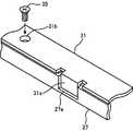
次に液晶セル9の位置決め及び液晶セル9とバックシャーシ11の接合について説明する。図5は、液晶セル9とバックシャーシ11の接合関係を示した斜視図である。液晶セル9の裏面9bの外周縁部に液晶セル支持部材27、28、29、30が接着または粘着される。液晶セル支持部材27、28、29、30は其々複数の第1の係合部27a、28a、29a、30aを有する。 Next, positioning of the liquid crystal cell 9 and joining of the liquid crystal cell 9 and the
接合部材31、32、33、34は、其々複数の第2の係合部31a、32a、33a、34aを有する。接合部材31、32、33、34の第2の係合部31a、32a、33a、34aが、液晶セル支持部材26、27、28、29の第1の係合部26a、27a、28a、29aと其々係合することによって、液晶セル支持部材に接合部材が接合する。 The joining
接合部材31、32、33、34は、其々複数の通孔31b、32b、33b、34bを有する。バックシャーシ11の壁部23a、23b、23c、23dは、其々複数のネジ孔26を有する。光源装置12、放熱板13、導光板14、反射シート15、光学シート16等が既に組み込まれたバックシャーシ11を接合部材31、32、33、34で形成された枠体の内側に嵌めこみ、ネジ35を外側から通孔31b、32b、33b、34bを通してネジ孔26に螺合させることにより、接合部材31、32、33、34を壁部23a、23b、23c、23dに接合する。 The joining
このようにして液晶セル9とバックシャーシ11を接合させることにより、図3に示した液晶モジュール4が形成される。図3に示したように、液晶モジュール4を前面側から見たとき、液晶モジュール4の外形は液晶セル9の外形と略同一である。 By bonding the liquid crystal cell 9 and the
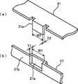
図6は、液晶セル支持部材27の外観斜視図である。図7は、液晶セル支持部材27、28、29、30が接着または粘着された液晶セル9を裏面9b側から見た斜視図である。液晶セル支持部材27は、細長い棒状であり、樹脂成型により形成されている。液晶セル支持部材は、液晶セル9の裏面9bの外周縁部の4辺の内で少なくとも3辺について各辺の一方の端部近辺から他の端部近辺に亘って設けられ、各外周縁部に接着または粘着されている。例えば、液晶セル支持部材27はこの部品1個で液晶セル9の上部の辺の一方の端部近辺から他の端部近辺に亘って設置されている。 FIG. 6 is an external perspective view of the liquid crystal
4辺の内で3辺に用いられる場合は、他の1辺については底部に当たる液晶セル支持部材30を用いず、底部に当たる辺にのみ液晶セル9を支持するベゼルが別途設けられる。ベゼルは液晶セル9の前面9aの底部の辺に沿う部分を挟み込むようにして支持する部材等が用いられる。図7においては、4辺について液晶セル支持部材が配置されているが、液晶セル支持部材27、30は液晶セル9の長辺に、液晶セル支持部材28、29は短辺にそれぞれ接着または粘着されている。 In the case where three of the four sides are used, the liquid crystal
液晶セル支持部材27の一面は接着面27bであり、接着面27bが液晶セル9の裏面9bの外周縁部に接着または粘着される。接着、粘着については液晶セル9の表面材質、表面状態、また、液晶セル支持部材27の材質、接着面27bの表面状態により適当な接着剤、粘着剤、接着テープや粘着テープを選択すればよい。接着面27は全面を接着または粘着してもよいし、または部分的に接着または粘着してもよい。接着面27全面を接着または粘着するか、部分的に接着または粘着するかについては適宜決めればよい。 One surface of the liquid crystal
液晶セル支持部材27は、略等間隔に第1の係合部27aが設けられている。第1の係合部27aは、液晶セル支持部材27を液晶セル9の長辺の外周縁部に接着したときに、液晶セル9の外側方向に開口部を有する凹部を構成する。図6においては、第1の係合部27aは8個設けられている。同様に液晶セル支持部材30の第1の係合部30aは8個、短辺の液晶セル支持部材28、29は其々4個設けられている。 The liquid crystal
液晶セル支持部材27は液晶セル9の長辺1辺に亘っている。同様に液晶セル支持部材30も長辺1辺に亘っている。液晶セル支持部材28、29は短辺1辺に亘っている。長辺あるいは短辺1辺に亘る部材とすることで、液晶セルの周辺に加わる不均一な応力を軽減することができる。また、液晶セル9を支持する際の強度を向上させると共に液晶セル9の外周縁部の強度を向上させることが可能である。 The liquid crystal
例えば、液晶セル支持部材27を係合部27a毎に8分割して、其々を液晶セル9の外周縁部に接着すると、分割された係合部の周囲に部分的な応力が生じ、長辺1辺に亘って不均一な応力が働く可能性がある。部分的な応力や不均一な応力が働くと表示面の外周部に輝度ムラが発生し、表示画像の品質が低下する。液晶セル支持部材27を1辺に亘るようにすることで部分的な応力や不均一な応力の発生を低減することができ、輝度ムラが発生しないようにすることができる。 For example, when the liquid crystal
図8は、31の外観斜視図である。接合部材31は、細長い棒状であり、板金あるいは樹脂により形成されている。接合部材は、液晶支持部材の其々と接合し、かつバックシャーシ11の其々の壁部の長手方向の両側の端部近辺に亘って接合する。液晶支持部材と同様に少なくとも3個が設けられている。接合部材31は、複数の第2の係合部31aを有する。第2の係合部31aは、接合部材31の接合面31cの方向に突出している。第2の係合部31aは、略等間隔に設けられている。この間隔は液晶セル支持部材27の第1の係合部27aの間隔と同じである。第2の係合部31aと液晶セル支持部材27の第1の係合部27aを係合させることによって、液晶セル支持部材27と接合部材31が接合する。図8においては、第2の係合部31aは8個設けられている。 FIG. 8 is an external perspective view of 31. The joining
同様に接合部材34の第2の係合部34aは8個、短辺用の接合部材32、33は其々4個設けられている。第2の係合部34aと液晶セル支持部材30の第1の係合部30aを係合させ、第2の係合部32aと液晶セル支持部材28の第1の係合部28aを係合させ、第2の係合部33aと液晶セル支持部材29の第1の係合部29aを係合させることによって、其々液晶セル支持部材と接合部材が接合する。 Similarly, the second
接合部材31の外側面31dには、複数の通孔31bを有する。図8においては、5個設けられている。同様に接合部材32は通孔32bが3個、接合部材33は通孔33bが3個、接合部材34は通孔34bが5個設けられている。通孔31bは、バックシャーシ11と接合部材31をネジ35によって接合するために用いられる。 The
図9は、液晶セル支持部材27の第1の係合部27aと接合部材31の第2の係合部31aを拡大した斜視図である。図9(a)は、接合部材31であり、図9(b)は、液晶セル支持部材27である。図10は、液晶セル支持部材27と接合部材31が係合した状態を示した斜視図である。第1の係合部27aの幅W1は第2の係合部31aの幅W2より大きく、第1の係合部27aの奥行T1は第2の係合部31aの厚さT2より大きい。 FIG. 9 is an enlarged perspective view of the
図10に示したように第1の係合部27aと第2の係合部31aが係合した状態で、ネジ35を、通孔31bを通してバックシャーシ11の壁部23aのネジ孔26に螺合させることにより、第1の係合部27aと第2の係合部31aの係合が離脱しない状態となり、バックシャーシ11に対して液晶セルが接合した状態となる。 As shown in FIG. 10, with the
図11は、液晶モジュール4の上部の部分断面図である。図3におけるCC断面図である。液晶セル9の裏面9bの外周縁部に、液晶セル支持部材27が接着または粘着されている。液晶セル支持部材27の第1の係合部27aと接合部材31の第2の係合部31aが係合している。バックシャーシ11には、反射シート15、導光板14、光学シート16が組み込まれ、中間押さえ枠17によって位置決めされている。接合部材31はバックシャーシ11にネジによって固定されている。 FIG. 11 is a partial cross-sectional view of the upper part of the liquid crystal module 4. It is CC sectional drawing in FIG. A liquid crystal
図11においては、液晶セル9の外周の上面9cと接合部材31の外側面31dは略同一面(略同一の高さ)である。外側面31dは上面9cに対して0mmから十数mm程度高い位置にあってもよい。本体2を囲むカバー7は、接合部材31の外側面31dに当接するようにバックシャーシ11に固定されている。カバー7の前端面7aは、液晶セル9の表示面9aと略同一な面の位置にある。 In FIG. 11, the
以上のような構成にすることで、液晶表示装置1を前面側から見たとき、液晶セル9の周囲には、カバー7の前端面7aだけが見えることになり、狭額縁化を実現することができる。なお、液晶セル9の下部だけカバー7の額縁が存在する場合もある。カバー7は、樹脂成型や板金加工により形成されることが一般的であり、カバー7の前端面7aを薄く加工することが可能である。 With the configuration as described above, when the liquid
以上のように、液晶セル9の裏面9bの外周縁部に各辺の両側の端部近辺に亘る液晶セル支持部材27、28、29、30を接着または粘着し、接合部材31、32、33、34を係合し、バックシャーシ11と接合することによって、液晶セル9の外形と略同等の外形の液晶モジュール4を形成することができ、カバー7の前端面7aを薄くすることで狭額縁化が可能となり、また、外周縁部の1辺に亘る液晶セル支持部材を用いることによって、液晶セル9に接着または粘着した場合でも、部分的な応力や不均一な応力の発生を低減することができ、輝度ムラが発生しないようにすることができる。 As described above, the liquid crystal
図12は、実施形態における液晶セル支持部材と接合部材の他の例を示した図である。図12(a)は、接合部材39であり、図12(b)は、液晶セル支持部材38である。液晶セル支持部材38と接合部材39の接合は嵌合ではなく、ネジ40による接合である。 FIG. 12 is a view showing another example of the liquid crystal cell support member and the joining member in the embodiment. FIG. 12A shows the joining
液晶セル支持部材38は、複数のネジ孔38aを有する。液晶セル9との接着面38bに対して略直角に突出した接合支持部38が設けられ、この接合支持部38の略中央にネジ孔38aが配置されている。図12(b)においては、8個設けられている。 The liquid crystal
接合部材39は、通孔39a、39bが其々複数設けられている。通孔39aは、液晶セル支持部材38と接合するためのもので、ネジ40を通孔39aを通して液晶セル支持部材38のネジ孔38a螺合することにより、液晶セル支持部材38と接合部材39を接合する。図12(a)においては、8個設けられている。通孔39bは、図8に示した通孔31bと同様の作用、機能を有する通孔である。以上のように、液晶セル支持部材38と接合部材39をネジ40による接合としてもよい。 The joining
なお、本発明は上記実施形態そのままに限定されるものではなく、実施段階ではその要旨を逸脱しない範囲で構成要素を変形して具現化できる。また、上記実施形態に開示されている複数の構成要素の適宜な組み合わせにより、種々の発明を形成できる。例えば、実施形態に示される全構成要素から幾つかの構成要素を削除してもよい。更に異なる実施形態に亘る構成要素を適宜組み合わせてもよい。 Note that the present invention is not limited to the above-described embodiments as they are, and can be embodied by modifying the constituent elements without departing from the scope of the invention in the implementation stage. In addition, various inventions can be formed by appropriately combining a plurality of components disclosed in the embodiment. For example, some components may be deleted from all the components shown in the embodiment. Furthermore, constituent elements over different embodiments may be appropriately combined.
1 液晶表示装置
2 本体
3 スタンド
4 液晶モジュール
5 回路基板
6 電源回路基板
7 カバー
8 画面
9 液晶セル
10 バックライト装置
11 バックシャーシ
12 光源装置
13 放熱板
14 導光板
15 反射シート
16 光学シート
17 中間押さえ枠
18 発光素子配線基板
19 発光素子
22 底部
23a、b、c、d 壁部
24 開口部
25 背面
26 ネジ孔
27、28、29、30 液晶セル支持部材
27a、28a、29a、30a 第1の係合部
27b、28b、29b、30b 接着面
31、32、33、34 接合部材
31a、32a、33a、34a 第2の係合部
31b、32b、33b、34b 通孔
35 ネジ
38 液晶セル支持部材
39 接合部材DESCRIPTION OF
Claims (7)
Translated fromJapanese前記液晶セルの映像表示面と反対側の裏面の外周縁部の4辺の内で少なくとも3辺について各辺の一方の端部近辺から他の端部近辺に亘って設けられ前記外周縁部に接着または粘着された少なくとも3個の液晶セル支持部材と、
外形が略長方形の底部と該底部の周囲に壁部を有する筐体と、
前記液晶セル支持部材と接合し、かつ前記筐体の其々の壁部の長手方向の一方の端部近辺から他の端部近辺に亘って接合する少なくとも3個の接合部材と、
を有する液晶モジュール。A transmissive liquid crystal cell having a substantially rectangular outer shape,
At least three of the four sides of the outer peripheral edge of the back surface opposite to the image display surface of the liquid crystal cell are provided from the vicinity of one end of each side to the vicinity of the other end. At least three liquid crystal cell support members bonded or adhered;
A casing having an outer shape having a substantially rectangular bottom and a wall around the bottom;
At least three joining members that are joined to the liquid crystal cell support member and joined from the vicinity of one end in the longitudinal direction of each wall of the housing to the vicinity of the other end;
A liquid crystal module.
前記液晶セルの映像表示面と反対側の裏面の外周縁部の4辺の内で少なくとも3辺について各辺の一方の端部近辺から他の端部近辺に亘って設けられ前記外周縁部に接着または粘着された少なくとも3個の液晶セル支持部材と、
外形が略長方形の底部と該底部の周囲に壁部を有する筐体と、
前記液晶セル支持部材と接合し、かつ前記筐体の其々の壁部の長手方向の一方の端部近辺から他の端部近辺に亘って接合する少なくとも3個の接合部材と、
前記液晶セルを駆動する電気回路基板と、
を有する液晶表示装置。A transmissive liquid crystal cell having a substantially rectangular outer shape,
At least three of the four sides of the outer peripheral edge of the back surface opposite to the image display surface of the liquid crystal cell are provided from the vicinity of one end of each side to the vicinity of the other end. At least three liquid crystal cell support members bonded or adhered;
A casing having an outer shape having a substantially rectangular bottom and a wall around the bottom;
At least three joining members that are joined to the liquid crystal cell support member and joined from the vicinity of one end in the longitudinal direction of each wall of the housing to the vicinity of the other end;
An electric circuit board for driving the liquid crystal cell;
A liquid crystal display device.
Priority Applications (3)
| Application Number | Priority Date | Filing Date | Title |
|---|---|---|---|
| JP2012170640AJP2014029448A (en) | 2012-07-31 | 2012-07-31 | Liquid crystal module and liquid crystal display device |
| US13/895,560US20140036197A1 (en) | 2012-07-31 | 2013-05-16 | Liquid Crystal Module and Liquid Crystal Display Device |
| CN201310236468.6ACN103576349A (en) | 2012-07-31 | 2013-06-14 | Liquid crystal module and liquid crystal display device |
Applications Claiming Priority (1)
| Application Number | Priority Date | Filing Date | Title |
|---|---|---|---|
| JP2012170640AJP2014029448A (en) | 2012-07-31 | 2012-07-31 | Liquid crystal module and liquid crystal display device |
Publications (1)
| Publication Number | Publication Date |
|---|---|
| JP2014029448Atrue JP2014029448A (en) | 2014-02-13 |
Family
ID=50025159
Family Applications (1)
| Application Number | Title | Priority Date | Filing Date |
|---|---|---|---|
| JP2012170640APendingJP2014029448A (en) | 2012-07-31 | 2012-07-31 | Liquid crystal module and liquid crystal display device |
Country Status (3)
| Country | Link |
|---|---|
| US (1) | US20140036197A1 (en) |
| JP (1) | JP2014029448A (en) |
| CN (1) | CN103576349A (en) |
Cited By (5)
| Publication number | Priority date | Publication date | Assignee | Title |
|---|---|---|---|---|
| KR101769017B1 (en)* | 2016-02-02 | 2017-08-17 | 주식회사 화인알텍 | Cover device for a display module |
| JP2017227767A (en)* | 2016-06-22 | 2017-12-28 | 旭硝子株式会社 | Display device |
| JP2017227768A (en)* | 2016-06-22 | 2017-12-28 | 旭硝子株式会社 | Display device and method for manufacturing display device |
| JP2022043680A (en)* | 2020-09-04 | 2022-03-16 | 富士通クライアントコンピューティング株式会社 | Display device |
| JP2022081233A (en)* | 2020-11-19 | 2022-05-31 | アルプスアルパイン株式会社 | Display device |
Families Citing this family (6)
| Publication number | Priority date | Publication date | Assignee | Title |
|---|---|---|---|---|
| CN103792712A (en)* | 2014-01-20 | 2014-05-14 | 深圳市华星光电技术有限公司 | Cooling structure of liquid crystal display module |
| US9699436B2 (en)* | 2014-09-16 | 2017-07-04 | Microsoft Technology Licensing, Llc | Display with eye-discomfort reduction |
| JP6428089B2 (en)* | 2014-09-24 | 2018-11-28 | 日亜化学工業株式会社 | Light emitting device |
| CN106293561B (en)* | 2015-05-28 | 2020-02-28 | 北京智谷睿拓技术服务有限公司 | Display control method and device and display equipment |
| US11262839B2 (en) | 2018-05-17 | 2022-03-01 | Sony Interactive Entertainment Inc. | Eye tracking with prediction and late update to GPU for fast foveated rendering in an HMD environment |
| US10942564B2 (en) | 2018-05-17 | 2021-03-09 | Sony Interactive Entertainment Inc. | Dynamic graphics rendering based on predicted saccade landing point |
Family Cites Families (5)
| Publication number | Priority date | Publication date | Assignee | Title |
|---|---|---|---|---|
| JP5183075B2 (en)* | 2007-02-08 | 2013-04-17 | 株式会社ジャパンディスプレイイースト | Liquid crystal display |
| TW201027180A (en)* | 2009-01-15 | 2010-07-16 | Hannstar Display Corp | LCD apparatus with edge-engaging assembly and method of fabricating such edge-engaging assembly |
| JP4679659B2 (en)* | 2009-01-20 | 2011-04-27 | パナソニック株式会社 | Case structure of video display device |
| JP4659156B1 (en)* | 2010-07-01 | 2011-03-30 | オリオン電機株式会社 | Electronic equipment with a liquid crystal display panel |
| KR20120019140A (en)* | 2010-08-25 | 2012-03-06 | 삼성전자주식회사 | Liquid crystal display device |
- 2012
- 2012-07-31JPJP2012170640Apatent/JP2014029448A/enactivePending
- 2013
- 2013-05-16USUS13/895,560patent/US20140036197A1/ennot_activeAbandoned
- 2013-06-14CNCN201310236468.6Apatent/CN103576349A/enactivePending
Cited By (6)
| Publication number | Priority date | Publication date | Assignee | Title |
|---|---|---|---|---|
| KR101769017B1 (en)* | 2016-02-02 | 2017-08-17 | 주식회사 화인알텍 | Cover device for a display module |
| JP2017227767A (en)* | 2016-06-22 | 2017-12-28 | 旭硝子株式会社 | Display device |
| JP2017227768A (en)* | 2016-06-22 | 2017-12-28 | 旭硝子株式会社 | Display device and method for manufacturing display device |
| JP2022043680A (en)* | 2020-09-04 | 2022-03-16 | 富士通クライアントコンピューティング株式会社 | Display device |
| JP2022081233A (en)* | 2020-11-19 | 2022-05-31 | アルプスアルパイン株式会社 | Display device |
| JP7540121B2 (en) | 2020-11-19 | 2024-08-27 | アルプスアルパイン株式会社 | Display device |
Also Published As
| Publication number | Publication date |
|---|---|
| US20140036197A1 (en) | 2014-02-06 |
| CN103576349A (en) | 2014-02-12 |
Similar Documents
| Publication | Publication Date | Title |
|---|---|---|
| JP2014029448A (en) | Liquid crystal module and liquid crystal display device | |
| US9195087B2 (en) | Display device and television device | |
| CN104471305B (en) | Lighting device, display device and television receiving device | |
| TWI391740B (en) | Liquid crystal display apparatus and method for dust prevention of liquid crystal display apparatus and method for fabricating liquid crystal display apparatus | |
| US10768466B2 (en) | Display device | |
| CN102043276A (en) | Liquid crystal display (LCD) | |
| CN104520759B (en) | Display device and radiovisor | |
| JP2012208254A (en) | Illumination device for display device and display device | |
| JP5519758B2 (en) | Liquid crystal display | |
| CN104583675A (en) | Lighting device, display device and television receiving device | |
| KR20170092622A (en) | Liquid crystal panel, backlight module positioning adhesive structure and display | |
| WO2012073750A1 (en) | Illumination device, display device, and television reception device | |
| WO2014091979A1 (en) | Display device | |
| WO2013129244A1 (en) | Display device, and television receiver | |
| JP2011180287A (en) | Display device | |
| US9658390B2 (en) | Light source cover including groove and backlight assembly including the light source cover | |
| US20140092340A1 (en) | Liquid crystal display device and assembly method thereof | |
| CN104541101A (en) | Lighting apparatus, display apparatus, and television receiver | |
| KR101737054B1 (en) | Backlight assembly and display apparatus having the same | |
| JP2016045362A (en) | Display device | |
| WO2012176698A1 (en) | Lighting apparatus, display apparatus, and television receiver apparatus | |
| JP2013258071A (en) | Lighting device, display device, and television receiving apparatus | |
| JP2013171619A (en) | Display device, and television receiver | |
| JP5717675B2 (en) | Display device and television receiver | |
| WO2014007136A1 (en) | Illumination device, display device, and television receiving device |
Legal Events
| Date | Code | Title | Description |
|---|---|---|---|
| A711 | Notification of change in applicant | Free format text:JAPANESE INTERMEDIATE CODE: A712 Effective date:20140614 | |
| RD02 | Notification of acceptance of power of attorney | Free format text:JAPANESE INTERMEDIATE CODE: A7422 Effective date:20150216 | |
| RD04 | Notification of resignation of power of attorney | Free format text:JAPANESE INTERMEDIATE CODE: A7424 Effective date:20150218 |