JP2014022368A - Connector for circuit board soldering with allowable difference compensation member - Google Patents
Connector for circuit board soldering with allowable difference compensation memberDownload PDFInfo
- Publication number
- JP2014022368A JP2014022368AJP2013135059AJP2013135059AJP2014022368AJP 2014022368 AJP2014022368 AJP 2014022368AJP 2013135059 AJP2013135059 AJP 2013135059AJP 2013135059 AJP2013135059 AJP 2013135059AJP 2014022368 AJP2014022368 AJP 2014022368A
- Authority
- JP
- Japan
- Prior art keywords
- circuit board
- contact
- deformation
- insulator
- region
- Prior art date
- Legal status (The legal status is an assumption and is not a legal conclusion. Google has not performed a legal analysis and makes no representation as to the accuracy of the status listed.)
- Granted
Links
Images


Classifications
- H—ELECTRICITY
- H01—ELECTRIC ELEMENTS
- H01R—ELECTRICALLY-CONDUCTIVE CONNECTIONS; STRUCTURAL ASSOCIATIONS OF A PLURALITY OF MUTUALLY-INSULATED ELECTRICAL CONNECTING ELEMENTS; COUPLING DEVICES; CURRENT COLLECTORS
- H01R12/00—Structural associations of a plurality of mutually-insulated electrical connecting elements, specially adapted for printed circuits, e.g. printed circuit boards [PCB], flat or ribbon cables, or like generally planar structures, e.g. terminal strips, terminal blocks; Coupling devices specially adapted for printed circuits, flat or ribbon cables, or like generally planar structures; Terminals specially adapted for contact with, or insertion into, printed circuits, flat or ribbon cables, or like generally planar structures
- H01R12/70—Coupling devices
- H01R12/71—Coupling devices for rigid printing circuits or like structures
- H01R12/712—Coupling devices for rigid printing circuits or like structures co-operating with the surface of the printed circuit or with a coupling device exclusively provided on the surface of the printed circuit
- H—ELECTRICITY
- H01—ELECTRIC ELEMENTS
- H01R—ELECTRICALLY-CONDUCTIVE CONNECTIONS; STRUCTURAL ASSOCIATIONS OF A PLURALITY OF MUTUALLY-INSULATED ELECTRICAL CONNECTING ELEMENTS; COUPLING DEVICES; CURRENT COLLECTORS
- H01R12/00—Structural associations of a plurality of mutually-insulated electrical connecting elements, specially adapted for printed circuits, e.g. printed circuit boards [PCB], flat or ribbon cables, or like generally planar structures, e.g. terminal strips, terminal blocks; Coupling devices specially adapted for printed circuits, flat or ribbon cables, or like generally planar structures; Terminals specially adapted for contact with, or insertion into, printed circuits, flat or ribbon cables, or like generally planar structures
- H01R12/70—Coupling devices
- H01R12/7005—Guiding, mounting, polarizing or locking means; Extractors
- H01R12/7011—Locking or fixing a connector to a PCB
- H01R12/707—Soldering or welding
- H—ELECTRICITY
- H01—ELECTRIC ELEMENTS
- H01R—ELECTRICALLY-CONDUCTIVE CONNECTIONS; STRUCTURAL ASSOCIATIONS OF A PLURALITY OF MUTUALLY-INSULATED ELECTRICAL CONNECTING ELEMENTS; COUPLING DEVICES; CURRENT COLLECTORS
- H01R12/00—Structural associations of a plurality of mutually-insulated electrical connecting elements, specially adapted for printed circuits, e.g. printed circuit boards [PCB], flat or ribbon cables, or like generally planar structures, e.g. terminal strips, terminal blocks; Coupling devices specially adapted for printed circuits, flat or ribbon cables, or like generally planar structures; Terminals specially adapted for contact with, or insertion into, printed circuits, flat or ribbon cables, or like generally planar structures
- H01R12/70—Coupling devices
- H01R12/91—Coupling devices allowing relative movement between coupling parts, e.g. floating or self aligning
- H—ELECTRICITY
- H01—ELECTRIC ELEMENTS
- H01R—ELECTRICALLY-CONDUCTIVE CONNECTIONS; STRUCTURAL ASSOCIATIONS OF A PLURALITY OF MUTUALLY-INSULATED ELECTRICAL CONNECTING ELEMENTS; COUPLING DEVICES; CURRENT COLLECTORS
- H01R13/00—Details of coupling devices of the kinds covered by groups H01R12/70 or H01R24/00 - H01R33/00
- H01R13/62—Means for facilitating engagement or disengagement of coupling parts or for holding them in engagement
- H01R13/629—Additional means for facilitating engagement or disengagement of coupling parts, e.g. aligning or guiding means, levers, gas pressure electrical locking indicators, manufacturing tolerances
- H01R13/631—Additional means for facilitating engagement or disengagement of coupling parts, e.g. aligning or guiding means, levers, gas pressure electrical locking indicators, manufacturing tolerances for engagement only
- H01R13/6315—Additional means for facilitating engagement or disengagement of coupling parts, e.g. aligning or guiding means, levers, gas pressure electrical locking indicators, manufacturing tolerances for engagement only allowing relative movement between coupling parts, e.g. floating connection
- H—ELECTRICITY
- H01—ELECTRIC ELEMENTS
- H01R—ELECTRICALLY-CONDUCTIVE CONNECTIONS; STRUCTURAL ASSOCIATIONS OF A PLURALITY OF MUTUALLY-INSULATED ELECTRICAL CONNECTING ELEMENTS; COUPLING DEVICES; CURRENT COLLECTORS
- H01R43/00—Apparatus or processes specially adapted for manufacturing, assembling, maintaining, or repairing of line connectors or current collectors or for joining electric conductors
- H01R43/02—Apparatus or processes specially adapted for manufacturing, assembling, maintaining, or repairing of line connectors or current collectors or for joining electric conductors for soldered or welded connections
- H01R43/0256—Apparatus or processes specially adapted for manufacturing, assembling, maintaining, or repairing of line connectors or current collectors or for joining electric conductors for soldered or welded connections for soldering or welding connectors to a printed circuit board
- H—ELECTRICITY
- H01—ELECTRIC ELEMENTS
- H01R—ELECTRICALLY-CONDUCTIVE CONNECTIONS; STRUCTURAL ASSOCIATIONS OF A PLURALITY OF MUTUALLY-INSULATED ELECTRICAL CONNECTING ELEMENTS; COUPLING DEVICES; CURRENT COLLECTORS
- H01R13/00—Details of coupling devices of the kinds covered by groups H01R12/70 or H01R24/00 - H01R33/00
- H01R13/40—Securing contact members in or to a base or case; Insulating of contact members
- H01R13/405—Securing in non-demountable manner, e.g. moulding, riveting
- H01R13/415—Securing in non-demountable manner, e.g. moulding, riveting by permanent deformation of contact member
- H—ELECTRICITY
- H01—ELECTRIC ELEMENTS
- H01R—ELECTRICALLY-CONDUCTIVE CONNECTIONS; STRUCTURAL ASSOCIATIONS OF A PLURALITY OF MUTUALLY-INSULATED ELECTRICAL CONNECTING ELEMENTS; COUPLING DEVICES; CURRENT COLLECTORS
- H01R43/00—Apparatus or processes specially adapted for manufacturing, assembling, maintaining, or repairing of line connectors or current collectors or for joining electric conductors
- H01R43/16—Apparatus or processes specially adapted for manufacturing, assembling, maintaining, or repairing of line connectors or current collectors or for joining electric conductors for manufacturing contact members, e.g. by punching and by bending
Landscapes
- Engineering & Computer Science (AREA)
- Manufacturing & Machinery (AREA)
- Coupling Device And Connection With Printed Circuit (AREA)
Abstract
Description
Translated fromJapanese本発明は、1つの絶縁体及びその内部の収納空間に収納された少なくとも1つの縦長のコンタクトを有し、前記コンタクトは、回路基板に装着される前記絶縁体の脚部と前記絶縁体の頭部の間を伸長し、少なくとも1つの前記コンタクトは、前記絶縁体の頭部に接する前端、差込み部、主部、裸の半田域及び絶縁体の脚部に接する後端が順次連なって成る回路基板半田付け用コネクターに関する。 The present invention has one insulator and at least one vertically long contact housed in a housing space inside the insulator, and the contact includes a leg portion of the insulator mounted on a circuit board and a head of the insulator. A circuit in which at least one of the contacts is connected to a head of the insulator, an insertion portion, a main portion, a bare solder area, and a rear end of the insulator in order. The present invention relates to a board soldering connector.
コネクターにおける1つの問題は、回路基板への半田付けにより、ずれが生じても、ソケット又はプラグ状のコンタクトを問題なく収納部に配列された互いに差込みできるソケット・プラグ式コネクターを供給することである。特に、半田付けすべき回路基板半田付け用コネクターが多数のコンタクトを備えるか、又は複数のソケット及び/又はプラグコネクターが1つの回路基板に配置され、共通のプラグにより連結される場合に、この問題が生ずる。個々のコンタクトのずれ、従ってコンタクトを収納している絶縁体のずれは、回路基板、コネクターの製造許容差並びにソケット式又はプラグ式コネクターを回路基板の半田付けにより生成する。このことは、特に表面実装部品としての基板回路装着用コネクターにおいては大きな問題である。そのようなコネクターの絶縁体の位置が設計通りでないと、障害が生ずることがあり、空間又は隙間に収納された半田付けされたコネクターを、ハウジングのそれぞれの絶縁体に包み込み且つ/又は噛み合わせるか且つ/又は適合させる必要がある。 One problem with the connector is to provide a socket-plug connector that can be inserted into the housing without any problem with sockets or plug-like contacts, even if they are misaligned by soldering to the circuit board. . In particular, this problem occurs when the circuit board soldering connector to be soldered has a large number of contacts, or when multiple sockets and / or plug connectors are arranged on one circuit board and connected by a common plug. Will occur. Deviations of the individual contacts, and hence the insulators containing the contacts, are generated by circuit board, connector manufacturing tolerances and socket or plug type connectors by soldering the circuit board. This is a serious problem particularly in a board circuit mounting connector as a surface mount component. If the position of the insulation of such a connector is not as designed, a failure may occur and whether the soldered connector contained in the space or gap is wrapped and / or mated with the respective insulation of the housing. And / or needs to be adapted.
このような問題を解決するのに、それぞれの絶縁体にコンタクトを可動に収納することが知られている。例えば、特許文献1及び特許文献2に示されている。しかしながら、ここではコンタクトのずれは補正されていないので、半田付けされた回路基板用コンタクトを対応するコネクターのコンタクトと連結するには困難であり半田付けされた位置に大きな力が加わる。このため、最終的には半田付け位置が損傷することがある。更に、半田付けされた基板回路装着用コネクターのコンタクト及び/又は対応するコネクターのコンタクトが損傷して、使用できなくなることもある。 In order to solve such a problem, it is known that a contact is movably accommodated in each insulator. For example, it is shown in
上記の背景技術に基づき、本発明は、少なくとも回路基板半田付け用コネクターの回路基板に半田付けされたコンタクトと、金属製のコンタクトを収納する絶縁体の収納部との間の許容差の補償の可能性を提案することにある。 Based on the above-described background art, the present invention compensates for a tolerance between at least a contact soldered to a circuit board of a circuit board soldering connector and a housing portion of an insulator housing a metal contact. It is to propose a possibility.
上記課題は、以下の(1)〜(13)のいずれかの構成により解決される。 The said subject is solved by the structure in any one of the following (1)-(13).
(1)1つの絶縁体及びその内部の収納空間に収納された少なくとも1つの縦長のコンタクトを有する回路基板半田付け用コネクターであって、前記コンタクトは、回路基板に装着される前記絶縁体の脚部と前記絶縁体の頭部の間を伸長し、少なくとも1つの前記コンタクトは、前記絶縁体の頭部6に接する前端、差込み部、主部、裸の半田域及び前記絶縁体の脚部に接する後端が順次連なって成り、前記主部は、前記差込み部に連なる円筒状の曲げ難い係止域及び前記係止域と前記半田域の間を伸長している円筒状の変形し易い変形域から成り、前記変形域の変形により、少なくとも1つの前記コンタクトの前記差込み部は、前記半田域に対して横方向に可動であることを特徴とする回路基板半田付け用コネクター。 (1) A circuit board soldering connector having one insulator and at least one vertically long contact housed in a housing space inside the insulator, wherein the contact is a leg of the insulator mounted on the circuit board. And at least one of the contacts on the front end, the insertion portion, the main portion, the bare solder zone, and the leg portion of the insulator. The rear end in contact with each other is successively connected, and the main part is a cylindrical, non-bendable locking region connected to the insertion portion, and a cylindrical, easily deformable deformation extending between the locking region and the soldering region. A circuit board soldering connector, wherein the insertion portion of at least one of the contacts is movable laterally with respect to the solder area by deformation of the deformation area.
(2)前記主部の前記係止域は、前記コンタクトの前記差込み域を前記収納空間内に少なくとも横方向に動かないように固定し、前記絶縁体と少なくとも1つの前記コンタクトの間の前記収納空間内の前記変形域に環状空隙が形成され、前記変形域は、前記絶縁体に横方向の力が加わると前記環状空隙内へと変形可能であることを特徴とする前記(1)に記載の回路基板半田付け用コネクター。 (2) The locking area of the main part fixes the insertion area of the contact in the storage space so as not to move at least laterally, and the storage between the insulator and at least one of the contacts. The annular gap is formed in the deformation area in the space, and the deformation area can be deformed into the annular gap when a lateral force is applied to the insulator. Circuit board soldering connector.
(3)少なくとも1つの前記コンタクトは、少なくともその変形域部分は内部が空洞に形成されていることを特徴とする前記(1)又は(2)に記載の回路基板半田付け用コネクター。 (3) The circuit board soldering connector according to (1) or (2), wherein at least one of the contacts has at least a deformed area formed inside a cavity.
(4)前記変形域は、少なくとも1つの前記コンタクトの縦軸に対して横及び/又は斜めに伸長し、軸方向にずらして配置した2つの隙間を備え、それぞれの前記隙間は、前記変形域の周壁の少なくとも半分を伸長していることを特徴とする前記(3)に記載の回路基板半田付け用コネクター。 (4) The deformation area includes two gaps that extend laterally and / or obliquely with respect to the longitudinal axis of at least one of the contacts, and are displaced in the axial direction, and each of the gaps includes the deformation area. The circuit board soldering connector according to (3), wherein at least half of the peripheral wall of the circuit board is extended.
(5)前記隙間は、横スリット及び/又は斜スリット並びに前記コンタクトの縦軸に平行に伸長する縦スリットから成り、前記横スリット及び/又は前記斜スリットは、その末端が前記縦スリットの中心に連結されて噛み合っていることを特徴とする前記(4)に記載の回路基板半田付け用コネクター。 (5) The gap includes a horizontal slit and / or a diagonal slit and a vertical slit extending in parallel with the longitudinal axis of the contact, and the end of the horizontal slit and / or the diagonal slit is at the center of the vertical slit. The circuit board soldering connector according to (4), wherein the connector is connected and meshed.
(6)前記縦スリットは、前記横スリット及び/又は前記斜スリットよりも幅広であることを特徴とする前記(5)に記載の回路基板半田付け用コネクター。 (6) The circuit board soldering connector according to (5), wherein the vertical slit is wider than the horizontal slit and / or the oblique slit.
(7)軸方向にずらして配置された前記縦スリットは、上下に配置されていることを特徴とする前記(5)又は(6)に記載の回路基板半田付け用コネクター。 (7) The circuit board soldering connector according to (5) or (6), wherein the vertical slits arranged to be shifted in the axial direction are arranged vertically.
(8)前記隙間は、前記変形域の周辺域において、回転対称に互いにずらして配置されていることを特徴とする前記(4)ないし(7)のいずれか1項に記載の回路基板半田付け用コネクター。 (8) The circuit board soldering according to any one of (4) to (7), wherein the gaps are arranged so as to be rotationally symmetrical with respect to each other in the peripheral area of the deformation area. Connector.
(9)前記変形域は、前記コンタクトの縦方向に螺旋状に、前記変形域の前記周壁を少なくとも3/4に渉って伸長する少なくとも1つの前記隙間を備えていることを特徴とする前記(3)に記載の回路基板半田付け用コネクター。 (9) The deformation region includes at least one gap that extends in a spiral manner in the longitudinal direction of the contact and extends at least 3/4 of the peripheral wall of the deformation region. The circuit board soldering connector according to (3).
(10)少なくとも1つの前記コンタクトの少なくとも前記変形域は、塑性変形可能な材料から成ることを特徴とする前記(1)ないし(9)のいずれか1項に記載の回路基板半田付け用コネクター。 (10) The circuit board soldering connector according to any one of (1) to (9), wherein at least the deformation region of at least one of the contacts is made of a plastically deformable material.
(11)少なくとも1つの前記コンタクトは、一体部品として製造されていることを特徴とする前記(1)ないし(10)のいずれか1項に記載の回路基板半田付け用コネクター。 (11) The circuit board soldering connector according to any one of (1) to (10), wherein at least one of the contacts is manufactured as an integral part.
(12)少なくとも1つの前記コンタクトは、切削加工品、旋盤加工品又はプレス曲げ加工品であることを特徴とする前記(1)ないし(11)のいずれか1項に記載の回路基板半田付け用コネクター。 (12) The circuit board soldering device according to any one of (1) to (11), wherein the at least one contact is a cut product, a lathe product, or a press-bending product. connector.
(13)少なくとも2つの前記(1)ないし(12)のいずれか1項に記載の回路基板半田付け用コネクターを回路基板に半田付けしたコネクター配置。 (13) A connector arrangement in which the circuit board soldering connector according to any one of (1) to (12) is soldered to the circuit board.
本発明による回路基板半田付け用コネクターでは、差込み部がプラグ又はソケットを備え、差込み部及び回路基板に差込み又は表面実装用の半田域が形成されている。本発明では、主部が差込み部に連結している円筒状の曲げ難い係止域並びに半田域を伸長している円筒状の変形し易い変形域を備えているので、変形域が変形する際に、コンタクトの差込み部は半田域に対して横方向に動かすことができる。差込み部は、係止域を介して収納空間に導入され、絶縁体に横方向の力が加わって変形域が変形しても影響を受けない。半田域は、回路基板に半田付けされて固定されるので、位置及び形状が安定する。主部の係止域及び半田域に対する位置は、変形域が僅かな力により横方向に変形するように、設定することが好ましい。これにより、僅かな位置修正をするため、回路基板に対する絶縁体の横方向への移動が可能となり、コンタクトの差込み部は変形しない。 In the circuit board soldering connector according to the present invention, the insertion portion includes a plug or a socket, and a solder area for insertion or surface mounting is formed in the insertion portion and the circuit board. In the present invention, since the main part is provided with a cylindrical non-bending locking area connected to the insertion part and a cylindrical easily deformable deformation area extending the solder area, the deformation area is deformed. In addition, the contact plug can be moved laterally with respect to the solder area. The insertion portion is introduced into the storage space via the locking region, and is not affected even if the lateral force is applied to the insulator and the deformation region is deformed. Since the solder area is fixed by being soldered to the circuit board, the position and shape are stabilized. The positions of the main part with respect to the locking area and the solder area are preferably set so that the deformation area is deformed laterally by a slight force. Accordingly, since the position is slightly corrected, the insulator can be moved in the lateral direction with respect to the circuit board, and the contact insertion portion is not deformed.
変形域が、安定性の低い所定の部分を有することは目的に適っている。基本的には、差込み部が半田域に対して回路基板に平行な任意の方向に問題なく移動でき、半田された箇所とコンタクトの係止域との間において回路基板に対して垂直及び/又は平行な大きな力が生じないように所定の部分が形成、配置される。このようにして、僅かな位置ずれの場合には、絶縁体は常に収納部に連結することが可能であり、回路基板半田付け用コネクターの絶縁体の頭部において、差込み部のコンタクトは、対応するコネクターのコンタクトと常に連結可能となる。 It is suitable for the purpose that the deformation zone has a predetermined portion with low stability. Basically, the insertion portion can move without any problem in any direction parallel to the circuit board with respect to the solder area, and is perpendicular to the circuit board and / or between the soldered portion and the contact locking area. The predetermined portion is formed and arranged so that a large parallel force is not generated. In this way, in the case of a slight misalignment, the insulator can always be connected to the storage part, and the contact of the insertion part at the head of the insulator of the circuit board soldering connector is compatible. It is always possible to connect with the contact of the connector.
主部の係止域は、収納空間において少なくとも横方向に移動できないコンタクトの差込み部に固定されることが好ましく、収納空間の変形域における絶縁体とコンタクトの間に環状空隙が形成されて、絶縁体が横方向に押されると変形域は環状空隙内へと変形する。環状空隙により、変形域は収納空間の内壁と横方向の間隔が保たれるので、そこにおいて主部はコンタクトの縦軸に対して曲げ又は折り曲げることが可能となる。収納空間の壁は、ずれを限定する役割も果たしている。しかしながら、コンタクトの変形域を囲む収納空間の個々の壁を無くすことも可能である。十分な壁厚が確保できない小さな回路基板半田付け用コネクターでは、このことが避けがたい。全てのコンタクトに対する変形域は、半田域まで達する共通の1つの壁で囲まれ、共通の収納空間部分を形成する。 The locking area of the main part is preferably fixed to the insertion part of the contact that cannot move at least in the lateral direction in the storage space, and an annular gap is formed between the insulator and the contact in the deformation area of the storage space to When the body is pushed laterally, the deformation zone deforms into an annular gap. Due to the annular gap, the deformation zone is kept laterally spaced from the inner wall of the storage space, where the main part can be bent or bent with respect to the longitudinal axis of the contact. The wall of the storage space also plays a role of limiting the shift. However, it is also possible to eliminate individual walls of the storage space surrounding the deformation area of the contact. This is unavoidable for small circuit board soldering connectors where a sufficient wall thickness cannot be ensured. The deformation area for all the contacts is surrounded by a common wall that reaches the solder area and forms a common storage space portion.
軸方向に差込み部が伸長している主部の係止域を、収納空間に係止するか、押込むか、鋳込むか、又は別の方法により、固定してもよい。収納空間にコンタクトを固定する方法に応じて、係止域は、ほぼ遊びが無く固定される。収納空間内のコンタクトは、特に軸方向への動きが小さいので、例えば主部が横方向に曲げられるか、折り曲げられると、変形し易く形成された円筒状の変形域が変形する際に、係止域は収納空間に対して僅かしか移動しない。 The locking region of the main portion in which the insertion portion extends in the axial direction may be locked in the storage space, pushed, cast, or fixed by another method. Depending on the method of fixing the contact in the storage space, the locking area is fixed without play. Since the contact in the storage space has a particularly small movement in the axial direction, for example, when the main part is bent in the lateral direction or bent, the cylindrical deformation area formed easily deforms. The stop area moves only slightly relative to the storage space.
好適な実施態様では、回路基板半田付け用コネクターのコンタクトは、少なくともその変形域の内部が空洞に形成されている。好ましくは、円筒状に形成された空洞が在ることにより、変形域における主部の安定性が低下し、空洞は半田部まで続いている。この場合、空洞の径は、変形域の周壁は主部よりも薄いが、電流を通すのに十分なように、選定することが好ましい。これにより、変形域が変形し易くなり、差込み部の半田部に対する横方向へ移動が大きくできる。 In a preferred embodiment, the contact of the circuit board soldering connector has a cavity formed at least inside the deformation region. Preferably, the presence of the cavity formed in a cylindrical shape reduces the stability of the main part in the deformation region, and the cavity continues to the solder part. In this case, the diameter of the cavity is preferably selected so that the peripheral wall of the deformation region is thinner than the main part, but is sufficient to pass current. Thereby, the deformation area is easily deformed, and the movement of the insertion portion in the lateral direction with respect to the solder portion can be increased.
ある実施態様では、回路基板半田付け用コネクターの変形域は、コンタクトの縦軸に対して垂直及び/又は傾斜して、軸方向にずらして配置された少なくとも2つの隙間を備えている。それぞれの隙間は、変形域の周壁の少なくとも半分以上を伸長している。隙間は、変形域を主部の周壁及び/又は係止域を差込み部又は半田域に連結するそれぞれの変形域区分に分割する。変形域区分の連結位置は、特に変形域の変形し易い位置である。これにより、変形域区分が互いに傾いて、それぞれの隙間の大きさが増大及び/又は縮小する。この場合、変形域は、横方向のみ、斜方向のみ又は横方向及び斜方向に伸長する2つ又はそれ以上の隙間を備え、隙間が伸長する平面は、互いに0〜45°の任意の角度で且つコンタクトの縦軸に交わる。 In one embodiment, the deformation area of the circuit board soldering connector comprises at least two gaps that are perpendicular and / or inclined with respect to the longitudinal axis of the contacts and are offset in the axial direction. Each gap extends at least half or more of the peripheral wall of the deformation region. The gap divides the deformation area into respective deformation area sections that connect the peripheral wall of the main part and / or the locking area to the insertion part or the solder area. The connection position of the deformation area section is a position where the deformation area is particularly easily deformed. Thereby, the deformation zone sections are inclined to each other, and the size of each gap is increased and / or reduced. In this case, the deformation zone comprises two or more gaps extending only in the lateral direction, only in the oblique direction or in the lateral direction and in the oblique direction, and the planes in which the gaps extend are at an arbitrary angle of 0 to 45 ° with respect to each other. It intersects the vertical axis of the contact.
回路基板半田付け用コネクターの別の実施態様では、変形域は、コンタクトの縦軸方向に螺旋状に伸長する、少なくとも1つの隙間を備えている。この隙間は、変形域の周壁の少なくとも3/4以上に渉って周方向及び/又は軸方向に伸長する螺旋状スリットであることが好ましい。少なくとも1つの螺旋状の隙間が、変形域のほぼ全長に渉ってコンタクトの縦軸方向に伸長することが好ましい。2つ以上の螺旋状の隙間の場合には、主部の周方向並びに軸方向に互いにずれて配列される。これらの隙間が、変形域の周方向に回転対称にずれて配列されると、横方向の移動に対して優先する方向又は不利な方向が無くなるので、特に好ましい。変形域の螺旋状の隙間は、コンタクトの縦軸を横切るか及び/又は斜めに伸長する隙間と同様に作用する。 In another embodiment of the circuit board soldering connector, the deformation zone comprises at least one gap extending spirally in the longitudinal direction of the contact. This gap is preferably a spiral slit extending in the circumferential direction and / or the axial direction over at least 3/4 of the peripheral wall of the deformation region. Preferably, at least one helical gap extends in the longitudinal direction of the contact over substantially the entire length of the deformation zone. In the case of two or more spiral gaps, the gaps are arranged shifted from each other in the circumferential direction and the axial direction of the main part. It is particularly preferable that these gaps are arranged in a rotationally symmetrical manner in the circumferential direction of the deformation area because there is no preferred direction or disadvantageous direction with respect to the lateral movement. The helical gap in the deformation zone acts in the same way as a gap extending across the longitudinal axis of the contact and / or obliquely.
本発明の更に好適な実施態様では、隙間は、横スリット及び/又は斜スリット並びにコンタクトの縦軸に平行に伸長する縦スリットであり、横スリット及び/又は斜スリットはその末端が縦スリットの中心部と噛合って縦スリットに連結されことが好ましい。縦スリットを追加すると、変形域の剛性が更に低下する。追加の縦スリットは横及び/又は斜スリットよりも広く作成することが好ましい。これにより、変形域の変形に要する力は更に減ずることは明らかである。少なくとも2つの横及び/又は斜スリットによって形成される変形域区分は、互いに強く傾かせることが可能となる。そのため、差込み部は、半田域に対して横方向により大きく移動できる。 In a further preferred embodiment of the present invention, the gap is a transverse slit and / or an oblique slit and a longitudinal slit extending parallel to the longitudinal axis of the contact, and the lateral slit and / or the oblique slit has an end at the center of the longitudinal slit. It is preferable to be engaged with the portion and connected to the vertical slit. When a vertical slit is added, the rigidity of the deformation area is further reduced. The additional longitudinal slit is preferably made wider than the lateral and / or oblique slits. This clearly reduces the force required to deform the deformation region. The deformation zone sections formed by at least two lateral and / or oblique slits can be strongly tilted with respect to one another. Therefore, the insertion part can move largely in the lateral direction with respect to the solder area.
横及び/又は斜スリット末端と連結された縦スリットは軸方向に互いにずらして上下に配置することが好ましい。少なくとも2つの横及び/又は斜スリットを有する全ての実施態様では、隙間を変形域の周方向に互いに回転対称にずらして配置、すなわち変形域の周方向に均等に分配することが特に好ましいことが判明した。2つの横及び/又は斜スリットの場合には、隙間は互いに周方向に180°ずらして変形域に配置される。横及び/又は斜スリットの数が異なる場合には、360°/スリットの数の角度すらして配置する。これにより、差込み部を、半田域に対して回路基板に平行にあらゆる方向に均等に動かすことができるようになる。 It is preferable that the vertical slits connected to the ends of the horizontal and / or oblique slits are vertically displaced from each other in the axial direction. In all embodiments having at least two lateral and / or oblique slits, it is particularly preferred that the gaps are arranged in a rotationally symmetrical manner in the circumferential direction of the deformation zone, i.e. evenly distributed in the circumferential direction of the deformation zone. found. In the case of two lateral and / or oblique slits, the gaps are displaced in the circumferential direction by 180 ° and are arranged in the deformation zone. If the number of lateral and / or oblique slits is different, they are arranged at an angle of 360 ° / the number of slits. As a result, the insertion portion can be moved evenly in any direction parallel to the circuit board with respect to the solder area.
全ての実施態様において、本発明の提案する回路基板用コネクターは、1極の場合には、プラグ又はソケット形状の差込み部を有する1つのコンタクトを備え、多極の場合には、プラグ及び/又はソケット形状の差込み部を有する多数のコンタクトを備えている。多極の場合、差込み部、主部の係止域及び変形域並びにコンタクトの半田域のそれぞれを、同じ大きさ及び形状に形成するか且つ/又は異なった大きさ及び形状に形成してもよい。これらの実施態様において、回路基板用コネクターが1極又は多極であっても、少なくとも1つのコンタクトの少なくとも主部の変形域部分は変形し易い材料であることが好ましい。原則的に、差込み部及び/又は半田域は別の材料でもよく、通常の連結方法により、主部と電気的にも機械的にも連結できる。 In all embodiments, the proposed circuit board connector of the present invention comprises a single contact with a plug or socket shaped plug in the case of one pole, and a plug and / or in the case of multiple poles. A number of contacts having socket-shaped plugs are provided. In the case of a multi-pole, each of the insertion portion, the locking region and deformation region of the main portion, and the solder region of the contact may be formed in the same size and shape and / or in different sizes and shapes. . In these embodiments, even if the circuit board connector is one-pole or multi-pole, it is preferable that at least one deformation region portion of at least the main portion of the contact is a material that is easily deformed. In principle, the plug-in part and / or the solder zone may be made of a different material and can be electrically and mechanically connected to the main part by a normal connection method.
ある実施態様による多極の回路基板用コネクターでは、全てのコンタクトは、上述に特徴を伴った変形域を有する主部を備えている。複数のコンタクト又は変形域は、整列させた場合に相互に障害とならず且つ接触しないように配置されている。回路基板用コネクターの絶縁体を回路基板に対して整列することにより、1極並びに多極の場合も、間接的にコンタクトは相互に且つ基板に対しても整列される。この場合、変形域及び/又は半田域に絶縁体に、コンタクトを互いに電気的に隔離する隔壁を備えてもよい。いずれにせよ、コンタクトは、電気的に絶縁されて収納空間に収納されている。回路基板用コネクターの整列の際のコンタクトの変形を予防し且つ半田域のそれぞれの半田ピン又は半田パッドへの不必要な力がかかるのを防ぐためには、変形域の耐曲げ性又は耐座屈性は、主部の係止域又は半田域よりも遥かに小さい方が好ましい。 In one embodiment of the multipolar circuit board connector, all contacts have a main portion having a deformation zone characterized by the above. The plurality of contacts or deformation zones are arranged so that they do not interfere with each other and do not come into contact when aligned. By aligning the insulation of the circuit board connector with respect to the circuit board, the contacts are indirectly aligned with each other and with respect to the board even in the case of one pole and multiple poles. In this case, a partition for electrically isolating the contacts from each other may be provided in the insulator in the deformation region and / or the solder region. In any case, the contact is electrically insulated and stored in the storage space. In order to prevent contact deformation when aligning circuit board connectors and to avoid applying unnecessary force to each solder pin or solder pad in the solder area, bending resistance or buckling resistance in the deformation area is required. The property is preferably much smaller than the locking area or solder area of the main part.
本発明による回路基板用コネクターのコンタクトは、特に切削加工品、旋盤加工品又は打抜きロール曲げ加工品として製造される。このような部品は、周知の方法により安価に製造できる。特に打抜きロール曲げ加工コンタクトでは、ロール加工の前に、横、斜行、縦又は螺旋状のスリットを打抜き加工する。これにより、あらゆる形状及び配置が可能となる。 The contact of the circuit board connector according to the present invention is produced in particular as a cut product, a lathe product or a punched roll bending product. Such parts can be manufactured inexpensively by known methods. In particular, in a punching roll bending contact, a horizontal, oblique, vertical or spiral slit is punched before roll processing. Thereby, all shapes and arrangements are possible.
本発明によるコネクターの配置では、回路基板に半田付けされた少なくとも2つの回路基板用コネクターを備えている。そのような回路基板に半田付けされた少なくとも2つの回路基板用コネクターでは、主部の変形域の配列によりもたらされる許容差補償に大きな効果を及ぼす。 The connector arrangement according to the invention comprises at least two circuit board connectors soldered to the circuit board. At least two circuit board connectors soldered to such a circuit board have a significant effect on the tolerance compensation provided by the arrangement of the deformation areas of the main part.
以下、図面を用いて本発明による実施例の特徴及び長所を説明する。 Hereinafter, features and advantages of embodiments according to the present invention will be described with reference to the drawings.
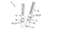
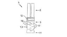
図1は、例として、多極の回路基板(不図示)装着用コネクター1の縦断面を示す斜視図である。回路基板半田付け用コネクター1は、絶縁体2並びに収納空間3に収納された複数の縦長のコンタクト4を備えている。コンタクト4は、絶縁体2の回路基板に接する脚部5と逆側の頭部6の間を伸長している。複数のコンタクト4は同一形状であり、絶縁体2の頭部6に接する前端7に連なる差込み部8、それに連結する主部9、並びに絶縁体2の脚部5に接する後端10に連なる半田域11を備えている。主部9は、差込み部8に接する円筒状の曲げ難い係止域12並びに係止域12と半田域11の間を伸長している円筒状の変形し易い変形域13から成っている。このため、変形域13の変形により、コンタクト4の差込み部8を、半田域11に対して、又は絶縁体2を回路基板に対して横方向に動かすことができる。 FIG. 1 is a perspective view showing a longitudinal section of a
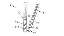
主部9の係止域12は、コンタクト4の差込み部8を収納空間3内に動かないように固定する。絶縁体2とそれぞれのコンタクト4の変形域13の間の収納空間3の中及び/又は該収納空間の下に環状空隙14が形成されている。これにより、絶縁体2に横方向の力が加わると変形域13は、環状空隙14内へと変形可能となる。コンタクト4は、その変形域13が中空に形成され且つ先端部7に接する差込み部8の部分にバネコンタクト15を備えている。本発明の回路基板半田付け用コネクター1のコンタクト4は、プレス曲げ加工部材が好ましい。実施例によっては、旋盤加工部材として形成してもよい。図2a〜図2eは、コンタクト4の例をそれぞれ2つ示す。 The locking
図2a〜図2eに図示した実施例のコンタクト4は、材料の条を打ち抜いてロール加工したものである。コンタクト4は、塑性加工可能な材料から製造した一体部品である。材料の条の厚さは、通常は0.25〜0.4mmである。変形域13の高さが5mm、その直径が約1.5mmの実施例では、変形域13を曲げるか又は折ると、差込み部8は、半田域11対して少なくとも側方の2つの方向に約0.35mmずれる。 The
図2a、2cに示す例のコンタクト4は、1つの変形域13に、コンタクト4の縦軸に対し直交する軸方向にずらして配置した2つの隙間16を備えている。それぞれの隙間16は、変形域13の周壁18の半分の表面に伸長している。隙間16は、変形域13を主部9の周壁18並びに/又は係止域12を差込み部8又は半田域11に連結する個々の変形域区分17に分割する。変形域区分17を、図3a〜3e、図4a〜4cに図示する。この変形域区分17の連結部は特に変形し易い。これにより、変形域区分17が互いに傾いて、隙間16の大きさ及び形状が変化する(図4a〜4c参照)。 The
円形の変形域13を有する図2a〜2eに示すコンタクト4では、隙間16を、スリットとして形成している。図2a、2cに示すコンタクト4の変形域13は、主部9の軸方向にずらして配置された、複数の横スリット19を備えている。横スリット19に加えて、縦方向に伸長する縦スリット20を備えてもよく、横スリット19の端部は縦スリット20の中心と連結され互いに噛み合っている。ここでは、縦スリット20は、横スリット19よりも幅広である。図2aでは、横スリット19に連結するそれぞれの縦スリット20は、変形域の外周に互いに並んで配置されている。図2cでは、2つの縦スリット20は、上下に配置されている。 In the
図2bは、横スリット19の代わりに、斜スリット21をとしての隙間16を備えた管状の変形域13を図示している。斜スリット21は、コンタクト4の縦軸に対して傾斜して伸長している。2つの斜スリット21は、軸方向にずれて配置され、変形域13の周壁18の少なくとも半分の表面を伸長している。この実施例では、縦スリットは備えていないが、原理的には備えることが可能である。 FIG. 2 b shows a
横スリット19及び/又は斜スリット21の代わりに、変形域13は、螺旋状にコンタクト4の縦方向に伸長する少なくとも1つの隙間16、好ましくは少なくとも変形域13の周壁18を3/4に渉って伸長する螺旋状スリット22を備えてもよい。コンタクト4の縦方向に、変形域13の全長に渉って少なくとも1つの螺旋状スリット22が伸長していることが好ましい。図2dは、そのような1つ螺旋状スリット22を有するコンタクトの例、図2eは、2つの螺旋状スリット22を有する例を示している。隙間16として形成した螺旋状スリット22は、横スリット19又は斜スリット21と同様に作用する。図2a〜2eに示すコンタクト4、すなわち、隙間16の全ての例、特に横スリット19、斜スリット21又は螺旋状スリット22は、変形域13の中心軸に対して回転対称である。 Instead of the lateral slits 19 and / or the oblique slits 21, the
図3a〜3eは、図2a〜2eに示すコンタクト4の展開図である。ここでは、隙間16の変形域13における大きさ、形状、配置及び伸長状態は、図2よりも明瞭に図示されている。特に、差込み部8、主部9及び半田域11、又特に変形域の長さと大きさの関係は、図2よりも明瞭に図示されている。 3a to 3e are development views of the
図4a〜4cは、図2a〜2cに示すコンタクト4の変形域13の部分拡大図である。これらの図から、3つのそれぞれの変形域区分17は互いに傾いていることは明らかであり、外側の2つの向きは互いに平行である。これにより、差込み部8は半田域11に対し側方にずれることになる。図4の横スリット19、傾斜スリット21及び/又は縦スリット20の形状としての隙間16は、図2及び図3に示すものとは異なっていることは明らかである。 4a to 4c are partial enlarged views of the
1 回路基板半田付け用コネクター
2 絶縁体
3 収納空間
4 コンタクト
5 (絶縁体の)脚部
6 (絶縁体の)頭部
7 (コンタクトの)前端
8 差込み部
9 主部
10 (コンタクトの)後端
11 半田域
12 係止域
13 変形域
14 環状空間
15 バネコンタクト
16 隙間
17 変形域区分
18 周壁
19 横スリット
20 縦スリット
21 斜スリット
22 螺旋状スリットDESCRIPTION OF
Claims (13)
Translated fromJapanese前記コンタクトは、回路基板に装着される絶縁体(2)の脚部(5)と絶縁体(2)の頭部(6)の間を伸長し、
少なくとも1つのコンタクト(4)は、絶縁体の頭部(6)に接する前端(7)、差込み部(8)、主部(9)、裸の半田域(11)及び絶縁体の脚部(5)に接する後端(10)が順次連なって成り、
主部(9)は、差込み部(8)に連なる円筒状の曲げ難い係止域(12)及び係止域(12)と半田域(11)の間を伸長している円筒状の変形し易い変形域(13)から成り、変形域(13)の変形により、少なくとも1つのコンタクト(4)の差込み部(8)は、半田域(11)に対して横方向に可動であることを特徴とする回路基板半田付け用コネクター。A circuit board soldering connector having one insulator (2) and at least one vertically long contact (4) housed in a housing space (3) therein,
The contact extends between the leg (5) of the insulator (2) attached to the circuit board and the head (6) of the insulator (2),
At least one contact (4) has a front end (7) in contact with the insulator head (6), a plug (8), a main part (9), a bare solder zone (11) and an insulator leg ( 5) and the rear end (10) in contact with 5)
The main portion (9) is a cylindrical non-bending engaging region (12) connected to the insertion portion (8), and a cylindrical deformation extending between the engaging region (12) and the solder region (11). It is composed of an easily deformable region (13), and the deformed region (13) deforms, so that the insertion portion (8) of at least one contact (4) is movable laterally with respect to the solder region (11). Circuit board soldering connector.
絶縁体(2)と少なくとも1つのコンタクト(4)の間の収納空間(3)内の変形域(13)に環状空隙(14)が形成され、
変形域(13)は、絶縁体(2)に横方向の力が加わると環状空隙(14)内へと変形可能であることを特徴とする請求項1に記載の回路基板半田付け用コネクター。The locking area (12) of the main part (9) fixes the insertion area (8) of the contact (4) in the storage space (13) so as not to move at least laterally,
An annular gap (14) is formed in the deformation zone (13) in the storage space (3) between the insulator (2) and the at least one contact (4);
The circuit board soldering connector according to claim 1, wherein the deformation region (13) is deformable into the annular gap (14) when a lateral force is applied to the insulator (2).
それぞれの隙間(16)は、変形域(13)の周壁(18)の少なくとも半分を伸長していることを特徴とする請求項3に記載の回路基板半田付け用コネクター。The deformation zone (13) comprises two gaps (16) that extend laterally and / or obliquely with respect to the longitudinal axis of at least one contact (4) and are offset in the axial direction,
The circuit board soldering connector according to claim 3, wherein each gap (16) extends at least half of the peripheral wall (18) of the deformation zone (13).
横スリット(19)及び/又は斜スリット(21)は、その末端が縦スリット(20)の中心に連結されて噛み合っていることを特徴とする請求項4に記載の回路基板半田付け用コネクター。The gap (16) consists of a transverse slit (19) and / or a diagonal slit (21) and a longitudinal slit (20) extending parallel to the longitudinal axis of the contact (4),
5. The circuit board soldering connector according to claim 4, wherein the lateral slit (19) and / or the oblique slit (21) are engaged with each other at the end thereof connected to the center of the vertical slit (20).
Applications Claiming Priority (2)
| Application Number | Priority Date | Filing Date | Title |
|---|---|---|---|
| EP20120401161EP2690721B1 (en) | 2012-07-23 | 2012-07-23 | Electrical connector assembly soldered on a circuit board with tolerance compensation |
| EP12401161.0 | 2012-07-23 |
Publications (2)
| Publication Number | Publication Date |
|---|---|
| JP2014022368Atrue JP2014022368A (en) | 2014-02-03 |
| JP5657750B2 JP5657750B2 (en) | 2015-01-21 |
Family
ID=47071207
Family Applications (1)
| Application Number | Title | Priority Date | Filing Date |
|---|---|---|---|
| JP2013135059AExpired - Fee RelatedJP5657750B2 (en) | 2012-07-23 | 2013-06-27 | Circuit board soldering connector and connector layout |
Country Status (5)
| Country | Link |
|---|---|
| US (1) | US9147953B2 (en) |
| EP (1) | EP2690721B1 (en) |
| JP (1) | JP5657750B2 (en) |
| CN (1) | CN103579802B (en) |
| PL (1) | PL2690721T3 (en) |
Cited By (3)
| Publication number | Priority date | Publication date | Assignee | Title |
|---|---|---|---|---|
| US10724426B2 (en) | 2016-07-15 | 2020-07-28 | Ihi Corporation | Electric turbocharger |
| JP2022093257A (en)* | 2020-12-11 | 2022-06-23 | 矢崎総業株式会社 | Connector and terminal fittings |
| US12095214B2 (en) | 2020-12-11 | 2024-09-17 | Yazaki Corporation | Connector and terminal fitting |
Families Citing this family (4)
| Publication number | Priority date | Publication date | Assignee | Title |
|---|---|---|---|---|
| CN106363312B (en)* | 2016-11-23 | 2019-03-08 | 京信通信技术(广州)有限公司 | Weld matrix |
| CN106602329B (en)* | 2017-01-20 | 2018-12-11 | 南京物联传感技术有限公司 | A kind of wiring of exempting from for smart lock is telescopically connected to device |
| CN106848666B (en)* | 2017-03-18 | 2023-07-14 | 昆山惠禾新能源科技有限公司 | Plug terminals, socket terminals and components thereof |
| BE1028071B1 (en)* | 2020-02-19 | 2021-09-13 | Phoenix Contact Gmbh & Co | Electrical contact element |
Citations (4)
| Publication number | Priority date | Publication date | Assignee | Title |
|---|---|---|---|---|
| JPH0284289U (en)* | 1988-12-19 | 1990-06-29 | ||
| JPH0423068U (en)* | 1990-06-14 | 1992-02-25 | ||
| US5769652A (en)* | 1996-12-31 | 1998-06-23 | Applied Engineering Products, Inc. | Float mount coaxial connector |
| WO2012035030A1 (en)* | 2010-09-13 | 2012-03-22 | Hachadorian Design & Calculation Gmbh | Electrical contact |
Family Cites Families (8)
| Publication number | Priority date | Publication date | Assignee | Title |
|---|---|---|---|---|
| US3992076A (en)* | 1975-06-10 | 1976-11-16 | E. I. Du Pont De Nemours And Company | Circuit board socket |
| IT1179895B (en)* | 1984-12-28 | 1987-09-16 | Burndy Electra Spa | FEMALE ELECTRIC CONTACT ELEMENT WITH RELATIVELY REDUCED COUPLING EFFORT AND RELATIVE CONNECTOR COMPLEX |
| GB9127052D0 (en)* | 1991-12-20 | 1992-02-19 | Amp Gmbh | Stamped and formed sealed pin |
| US5692928A (en) | 1996-05-10 | 1997-12-02 | Molex Incorporated | Electrical connector having terminals with improved retention means |
| DE10261521B3 (en)* | 2002-12-23 | 2004-09-16 | Robert Bosch Gmbh | High-current contact elements with offset compensation |
| US6846185B1 (en)* | 2003-08-14 | 2005-01-25 | Lite-On Technology Corporation | Blind mating apparatus |
| DE102005013282A1 (en) | 2005-03-22 | 2006-09-28 | Rosenberger Hochfrequenztechnik Gmbh & Co. Kg | Connectors |
| US8033877B2 (en)* | 2008-07-22 | 2011-10-11 | Centipede Systems, Inc. | Connector for microelectronic devices |
- 2012
- 2012-07-23PLPL12401161Tpatent/PL2690721T3/enunknown
- 2012-07-23EPEP20120401161patent/EP2690721B1/ennot_activeNot-in-force
- 2013
- 2013-06-26USUS13/927,469patent/US9147953B2/ennot_activeExpired - Fee Related
- 2013-06-27JPJP2013135059Apatent/JP5657750B2/ennot_activeExpired - Fee Related
- 2013-07-23CNCN201310310330.6Apatent/CN103579802B/ennot_activeExpired - Fee Related
Patent Citations (4)
| Publication number | Priority date | Publication date | Assignee | Title |
|---|---|---|---|---|
| JPH0284289U (en)* | 1988-12-19 | 1990-06-29 | ||
| JPH0423068U (en)* | 1990-06-14 | 1992-02-25 | ||
| US5769652A (en)* | 1996-12-31 | 1998-06-23 | Applied Engineering Products, Inc. | Float mount coaxial connector |
| WO2012035030A1 (en)* | 2010-09-13 | 2012-03-22 | Hachadorian Design & Calculation Gmbh | Electrical contact |
Cited By (4)
| Publication number | Priority date | Publication date | Assignee | Title |
|---|---|---|---|---|
| US10724426B2 (en) | 2016-07-15 | 2020-07-28 | Ihi Corporation | Electric turbocharger |
| JP2022093257A (en)* | 2020-12-11 | 2022-06-23 | 矢崎総業株式会社 | Connector and terminal fittings |
| JP7395546B2 (en) | 2020-12-11 | 2023-12-11 | 矢崎総業株式会社 | Connectors and terminal fittings |
| US12095214B2 (en) | 2020-12-11 | 2024-09-17 | Yazaki Corporation | Connector and terminal fitting |
Also Published As
| Publication number | Publication date |
|---|---|
| CN103579802B (en) | 2016-08-10 |
| EP2690721A1 (en) | 2014-01-29 |
| US9147953B2 (en) | 2015-09-29 |
| CN103579802A (en) | 2014-02-12 |
| EP2690721B1 (en) | 2015-01-14 |
| PL2690721T3 (en) | 2015-08-31 |
| JP5657750B2 (en) | 2015-01-21 |
| US20140024232A1 (en) | 2014-01-23 |
Similar Documents
| Publication | Publication Date | Title |
|---|---|---|
| JP5657750B2 (en) | Circuit board soldering connector and connector layout | |
| JP7032499B2 (en) | Floating socket connector | |
| JP6553843B2 (en) | connector | |
| JP6041107B2 (en) | Coaxial connector with floating mechanism | |
| JP5360271B1 (en) | Electrical connector | |
| CN112086780B (en) | Sandwich type electric connector | |
| KR101762556B1 (en) | Connector | |
| JP5903726B2 (en) | Cable connector and connector device having the cable connector | |
| US20170331235A1 (en) | Connector | |
| US9106009B2 (en) | Electrical contact and electrical connector assembly including the same | |
| JP2013093124A (en) | Electric connector assembly | |
| JP6190348B2 (en) | Connector support structure and adapter | |
| US10312608B2 (en) | Insulation displacement connector | |
| JP2017103119A (en) | Electrical connector | |
| JP2013191556A (en) | Connector provided with allowable difference compensation member | |
| JP7463739B2 (en) | SOCKET, CONTACT UNIT, SOCKET AGGREGATE, AND MULTI-POINT CONNECTOR HAVING CONTACT UNIT | |
| CN106575829B (en) | cable connector | |
| US9385451B2 (en) | Connector housing, electric connector and method of inserting connector terminal into connector housing | |
| JP7139929B2 (en) | harness parts | |
| JP7312554B2 (en) | movable connector | |
| US9685725B2 (en) | Connector | |
| WO2015159964A1 (en) | Connector | |
| JP2022177863A (en) | crimp terminal | |
| JP2002025654A (en) | Electric connector assembly | |
| KR20150004087A (en) | Receptacle connector and connector assembly including the same |
Legal Events
| Date | Code | Title | Description |
|---|---|---|---|
| A977 | Report on retrieval | Free format text:JAPANESE INTERMEDIATE CODE: A971007 Effective date:20140716 | |
| A131 | Notification of reasons for refusal | Free format text:JAPANESE INTERMEDIATE CODE: A131 Effective date:20140729 | |
| A521 | Request for written amendment filed | Free format text:JAPANESE INTERMEDIATE CODE: A523 Effective date:20141017 | |
| TRDD | Decision of grant or rejection written | ||
| A01 | Written decision to grant a patent or to grant a registration (utility model) | Free format text:JAPANESE INTERMEDIATE CODE: A01 Effective date:20141111 | |
| A61 | First payment of annual fees (during grant procedure) | Free format text:JAPANESE INTERMEDIATE CODE: A61 Effective date:20141126 | |
| R150 | Certificate of patent or registration of utility model | Ref document number:5657750 Country of ref document:JP Free format text:JAPANESE INTERMEDIATE CODE: R150 | |
| R250 | Receipt of annual fees | Free format text:JAPANESE INTERMEDIATE CODE: R250 | |
| R250 | Receipt of annual fees | Free format text:JAPANESE INTERMEDIATE CODE: R250 | |
| R250 | Receipt of annual fees | Free format text:JAPANESE INTERMEDIATE CODE: R250 | |
| R250 | Receipt of annual fees | Free format text:JAPANESE INTERMEDIATE CODE: R250 | |
| R250 | Receipt of annual fees | Free format text:JAPANESE INTERMEDIATE CODE: R250 | |
| R250 | Receipt of annual fees | Free format text:JAPANESE INTERMEDIATE CODE: R250 | |
| LAPS | Cancellation because of no payment of annual fees |