JP2014016424A - Image display medium and image display device - Google Patents
Image display medium and image display deviceDownload PDFInfo
- Publication number
- JP2014016424A JP2014016424AJP2012152918AJP2012152918AJP2014016424AJP 2014016424 AJP2014016424 AJP 2014016424AJP 2012152918 AJP2012152918 AJP 2012152918AJP 2012152918 AJP2012152918 AJP 2012152918AJP 2014016424 AJP2014016424 AJP 2014016424A
- Authority
- JP
- Japan
- Prior art keywords
- electrode
- image display
- photoconductive layer
- pixel
- light
- Prior art date
- Legal status (The legal status is an assumption and is not a legal conclusion. Google has not performed a legal analysis and makes no representation as to the accuracy of the status listed.)
- Granted
Links
Images


Landscapes
- Electrochromic Elements, Electrophoresis, Or Variable Reflection Or Absorption Elements (AREA)
Abstract
Translated fromJapaneseDescription
Translated fromJapanese本発明は、画像表示媒体及び画像表示装置に関する。 The present invention relates to an image display medium and an image display device.
従来、メモリ性を有し繰り返し書換えが可能な画像表示媒体として、着色された電気泳動粒子を用いた画像表示媒体が知られている。このような画像表示媒体は、例えば一対の基板と、印加された電界により基板間を移動可能に基板間に封入されると共に、予め定めた色に着色されて帯電特性を有する電気泳動粒子と、を含んで構成される。 2. Description of the Related Art Conventionally, an image display medium using colored electrophoretic particles is known as an image display medium that has memory characteristics and can be rewritten repeatedly. Such an image display medium includes, for example, a pair of substrates, electrophoretic particles that are encapsulated between the substrates so as to be movable between the substrates by an applied electric field, are colored in a predetermined color, and have charging characteristics; It is comprised including.
このような画像表示媒体では、画像に応じた電圧を一対の基板間に印加することにより電気泳動粒子を移動させ、電気泳動粒子の色のコントラストとして画像を表示させる。また、画像を表示させた後に電圧の印加を停止した後も、画像表示は維持される。 In such an image display medium, the electrophoretic particles are moved by applying a voltage corresponding to the image between the pair of substrates, and the image is displayed as the color contrast of the electrophoretic particles. In addition, the image display is maintained even after the voltage application is stopped after the image is displayed.
このような電気泳動式の画像表示装置としては、例えば、特許文献1、2に記載の技術が提案されている。 As such an electrophoretic image display device, for example, techniques disclosed in Patent Documents 1 and 2 have been proposed.
特許文献1に記載の技術では、画素電極と共通電極との間に分散系を挟持して画素を構成して、TFTのゲート端子を走査線に接続し、ソース端子をデータ線に接続し、ドレイン端子を画素電極及び保持電極に接続して、TFTのオンオフにより各画素への電圧印加を制御する画像表示装置が提案されている。 In the technique described in Patent Document 1, a pixel is configured by sandwiching a dispersion system between a pixel electrode and a common electrode, a gate terminal of a TFT is connected to a scanning line, a source terminal is connected to a data line, An image display device has been proposed in which a drain terminal is connected to a pixel electrode and a holding electrode, and voltage application to each pixel is controlled by turning on and off the TFT.
一方、電気泳動式の画像表示媒体の駆動方式として、光照射による光書き込み方式が提案されている(例えば、特許文献2、3)。 On the other hand, an optical writing method using light irradiation has been proposed as a driving method for an electrophoretic image display medium (for example, Patent Documents 2 and 3).
特許文献2に記載の技術では、透光性を有する透光基板に配設された画素電極と、その画素電極に書き込むデータ信号を供給するデータ電極と、そのデータ電力および前記画素電極よりも前記透光基板側において、そのデータ電極と画素電極とにせ接続し、光が照射されることに起因して、データ電極と画素電極とを電気的に導通させる光導電体と、前記画素電極に対向して配置された対向電極と、その対向電極と前記画素電極との間に配置され、前記画素電極に書き込まれたデータ信号に応じて駆動される表示層とを備えた表示媒体が開示されている。 In the technique described in Patent Document 2, a pixel electrode disposed on a light-transmitting light-transmitting substrate, a data electrode that supplies a data signal to be written to the pixel electrode, the data power, and the pixel electrode On the light-transmitting substrate side, the data electrode and the pixel electrode are connected to each other, and the photoconductor that electrically connects the data electrode and the pixel electrode due to light irradiation is opposed to the pixel electrode. And a display layer disposed between the counter electrode and the pixel electrode and driven according to a data signal written to the pixel electrode is disclosed. Yes.
また、特許文献3に記載の技術では、非表示基板の外側に、光が照射されることにより導電性を示す光導電層を積層し、さらにその上に一様な電圧を印加できる電極付基板を形成し、電極付基板に直流電源により一様な電圧印加を行いながら、液晶透過パネル及び平板光電からなる露光装置により画像信号に基づいた潜像の露光を行い、そのパターンに従った分布を有する電界を与えることにより、粒子を移動させる画像表示媒体が提案されている。 Further, in the technique described in Patent Document 3, a substrate with an electrode that can stack a photoconductive layer that exhibits conductivity when irradiated with light on the outside of a non-display substrate and further apply a uniform voltage thereon. While applying a uniform voltage to the substrate with electrodes from a DC power source, the exposure device composed of a liquid crystal transmission panel and a flat panel photoelectric device exposes the latent image based on the image signal, and the distribution according to the pattern is obtained. An image display medium that moves particles by applying an electric field has been proposed.
本発明は、光書き込み電気泳動式の画像表示媒体における表示速度の高速化を図ることを目的とする。 An object of the present invention is to increase the display speed in an optical writing electrophoretic image display medium.
請求項1に記載の画像表示媒体は、それぞれ透光性を有する一対の基板と、前記一対の基板のうち一方の基板の他方の基板側上に形成された透光性を有する第1電極と、前記一対の基板のうち他方の基板の前記一方の基板側上に形成された透光性を有する第2電極と、前記第2電極の前記一方の基板側上に形成されて入射した光に応じて電気的特性が変化する光伝導層と、前記光伝導層の前記一方の基板側上に画素毎に形成された画素電極と、前記光伝導層の前記一方の基板側上の前記画素電極間に設けられ、前記一方の基板側から前記光伝導層への光を遮光する遮光層と、前記画素電極の前記一方の基板側上の一部に設けられた保持容量層と、前記保持容量層の前記一方の基板側上に形成された保持容量電極と、を備えている。 The image display medium according to claim 1, a pair of substrates having translucency, and a first electrode having translucency formed on the other substrate side of one of the pair of substrates. A light-transmitting second electrode formed on the one substrate side of the other substrate of the pair of substrates, and incident light formed on the one substrate side of the second electrode A photoconductive layer whose electrical characteristics change in response, a pixel electrode formed for each pixel on the one substrate side of the photoconductive layer, and the pixel electrode on the one substrate side of the photoconductive layer A light-blocking layer provided between the one substrate side and blocking light from the one substrate side to the photoconductive layer; a storage capacitor layer provided on a part of the pixel electrode on the one substrate side; and the storage capacitor And a storage capacitor electrode formed on the one substrate side of the layer.
請求項2に記載の画像表示装置は、請求項1に記載の画像表示媒体と、前記第1電極と前記第2電極とに電圧を印加する電圧印加手段と、前記他方の基板側から前記光伝導層へ光を照射する光照射手段と、画像情報に基づいて、前記電圧印加手段及び前記光照射手段を制御する制御手段と、を備えている。 According to a second aspect of the present invention, there is provided an image display device according to the first aspect, a voltage applying unit that applies a voltage to the first electrode and the second electrode, and the light from the other substrate side. A light irradiating means for irradiating the conductive layer with light; and a control means for controlling the voltage applying means and the light irradiating means based on image information.
請求項1に記載の発明によれば、本構成を採用しない場合と比較して、表示速度の高速化を図ることができる光書き込み電気泳動式の画像表示媒体を提供することができる、という効果がある。 According to the first aspect of the present invention, it is possible to provide an optical writing electrophoretic image display medium capable of increasing the display speed as compared with the case where this configuration is not adopted. There is.
請求項2に記載の発明によれば、本構成を採用しない場合と比較して、表示速度の高速化を図ることができる光書き込み電気泳動式の画像表示装置を提供することができる、という効果がある。 According to the second aspect of the present invention, it is possible to provide an optical writing electrophoretic image display device capable of increasing the display speed as compared with the case where this configuration is not adopted. There is.
以下、本発明の実施形態について図面を参照しつつ説明する。作用・機能が同じ働きを担う部材には、全図面を通して同じ符合を付与し、重複する説明を省略する場合がある。 Embodiments of the present invention will be described below with reference to the drawings. Members having the same functions and functions are given the same reference numbers throughout the drawings, and redundant descriptions may be omitted.
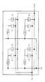
図1は、本発明の実施の形態に係わる画像表示装置の概略構成を示す図であり、図2は本発明の実施の形態に係わる画像表示媒体の画素部を表示面側から見た上面図である。なお、図1は、図2のA−A’断面を示す。 FIG. 1 is a diagram showing a schematic configuration of an image display apparatus according to an embodiment of the present invention, and FIG. 2 is a top view of the pixel portion of the image display medium according to the embodiment of the present invention as viewed from the display surface side. It is. FIG. 1 shows a cross section taken along line A-A ′ of FIG. 2.
本実施の形態に係わる画像表示装置10は、光を照射して電気泳動粒子を移動することにより画像を書き込む光書き込みタイプの画像表示装置10である。具体的には、光が照射さると電気的特性が変化する材料で構成された光伝導層24を有しており、画像を書き込む画素に対して光を照射することで当該画素の電気泳動粒子36へ電界を発生して画像を書き込むものである。 The
画像表示装置10は、図1に示すように、画像表示媒体12と、画像表示媒体12を駆動する駆動装置14と、を備えている。駆動装置14は、画像表示媒体12の表示面側となる共通透明電極18と背面側となる光伝導層用透明電極22との間に電圧を印加する電圧印加部32と、画像表示媒体12に表示させる画像に応じた光を照射する光照射部34と、画像表示媒体12に表示させるべき画像に応じて電圧印加部32及び光照射部34を制御する制御部30と、を含んで構成されている。 As shown in FIG. 1, the
制御部30は、画像情報に応じた電圧を各画素に印加するように電圧印加部32を制御すると共に、画像情報に応じた電圧を印加する画素に対して光を照射するように光照射部34を制御することにより、画像表示媒体12に画像を表示する。 The
画像表示媒体12は、表示面側とされた透明な表示基板16と、背面側とされた透明な背面基板20と、を有する一対の透明な基板を備えている。 The
表示基板16は、背面基板20側に透明な共通電極18が積層して形成されている。また、背面基板20は、表示基板16側に透明な光伝導層用透明電極22が積層して形成され、該光伝導層用透明電極22上に、光が照射されることにより電気的特性が変化する光伝導層24が積層して形成されている。 The display substrate 16 is formed by laminating a transparent
また、光伝導層24上には、画素毎に設けられる画素電極26が積層して形成されると共に、それぞれの画素電極26間に対して表示基板16側から光が光伝導層24に照射されないように、画素電極26の隣接する画素間を遮光するための遮光層28が積層して形成されている。 In addition, a
さらに、画素電極26上には、画素電極26の一部の領域に対して、保持容量を構成するための誘電体層40が積層して形成され、誘電体層40上に保持容量電極44が積層して形成されている。保持容量電極44は、図2に示すように、共通電極ライン42に結線して構成されている。すなわち、画素電極26の一部、誘電体層40、及び保持容量電極44によって保持容量部46が形成されている。 Further, on the
なお、誘電体層40は、実効的な画素部を広く確保できるように容量の値を設定する必要がある。例えば、開口率90%を確保する場合には、残り10%を遮光層28を含めた保持容量の領域として設計すればよい。そのためには、保持容量部46の誘電体層40の比誘電率εr、厚さd、面積Sによって保持容量Csの値が決定される(Cs=εS/d(ε=εr・ε0、ε0は真空の誘電率))。 The
また、上述のように構成された表示基板16と背面基板20との間には、規定の間隔を保持しながら、予め定めた色に着色され、基板間の電界に応じて移動する電気泳動粒子36が充填された分散媒38が充填されている。なお、図1では、電気泳動粒子36は一種類の場合を示すが、色及び帯電特性がそれぞれ異なる二種類以上の電気泳動粒子36を含むようにしてもよい。また、分散媒は、白等の予め定めた色に着色されていてもよい。 In addition, between the display substrate 16 and the
図3は、本発明の実施の形態に係わる画像表示媒体12における各画素の等価回路を示す図である。 FIG. 3 is a diagram showing an equivalent circuit of each pixel in the
上述のように構成された一対の基板は、図3に示す等価回路で表せる。すなわち、共通電極18と画素電極26によって画素容量Cpを構成し、共通電極18に共通電極電圧Vcomが印加される。 The pair of substrates configured as described above can be represented by an equivalent circuit shown in FIG. That is, the
また、光伝導層24が、光の照射によって抵抗が変化する画素抵抗Rpとされ、画素抵抗Rpには、画素容量Cpの画素電極26が接続されると共に、光伝導層用透明電極22が接続されて該光伝導層用透明電極22に光伝導層共通電圧Vaが印加される。 The
すなわち、光が照射された画素については、光伝導層共通電圧Vaが光伝導層24を介して画素電極26へ印加されることによって、基板間に電界が発生し、基板間の電界に応じて電気泳動粒子36が移動する。 That is, for the pixels irradiated with light, an electric field is generated between the substrates by applying the photoconductive layer common voltage Va to the
また、画素電極26の一部、誘電体層40、及び保持容量電極44によって形成された保持容量部46によって保持容量Csが構成され、保持容量電極44に共通電極ライン42に印加される保持容量用共通電圧Vsが印加される。すなわち、保持容量Csには、光伝導層24に光が照射された場合に、光伝導層用透明電極22に印加される光伝導層共通電圧Vaが画素電極26に印加され、共通電極ライン42に結線された保持容量電極44の保持容量用共通電圧Vsとの電位差によって電荷が蓄積される。従って、保持容量Csについても画像情報に応じた電荷が蓄積され、印加電圧が一定時間保持される。この一定時間保持される電圧によって、画素への光照射が終了しても、電気泳動粒子36には保持容量Csに電圧が印加され続けるため、応答速度の遅い電気泳動粒子36の駆動時間を、保持容量がない場合に比べて長く確保される。 In addition, a storage capacitor Cs is configured by a storage capacitor portion 46 formed by a part of the
一方、駆動装置14は、表示される画像に応じて、画像表示媒体12の一対の基板間に印加する電圧を制御すると共に、電圧を印加する画素を光照射によって選択することにより、電気泳動粒子36を泳動させ、表示基板16または背面基板20の何れか一方に引き付ける。 On the other hand, the driving
電圧印加部32は、共通電極18及び光伝導層用透明電極22にそれぞれ電気的に接続されていると共に、制御部30に接続されている。 The
光照射部34は、制御部30に接続されており、背面基板20側から画像情報に基づいて、画像を表示する画素に対して光を照射することにより、光伝導層用透明電極22に印加された電圧を光伝導層24を介して画素電極26へ印加する。 The
制御部30は、例えば、コンピュータとして構成される。コンピュータは、一例として、CPU(Central Processing Unit)、ROM(Read Only Memory)、RAM(Random Access Memory)、不揮発性メモリ、及び入出力インターフェース(I/O)がバスを介して各々接続された構成であり、I/Oに電圧印加部32が接続されると共に、光照射部34が接続される。この場合、画像表示に必要な電圧の印加を電圧印加部32に指示する処理をコンピュータに実行させるプログラムを、例えば不揮発性メモリに書き込んでおき、これをCPUが読み込んで実行させる。なお、プログラムは、CD−ROM等の記録媒体により提供するようにしてもよい。また、画像表示装置10に表示させる画像は、CD−ROMやDVD等の各種記録媒体やネットワーク等の通信手段を介して取得して制御部30に取り込んでもよい。 The
続いて、上述のように構成された本発明の実施の形態に係わる画像表示装置10の動作について説明する。図4は、光照射部34の光照射、光伝導層用透明電極の共通電圧Va、及び保持容量電極の保持容量用共通電圧Vsの一例を示す図である。なお、保持容量電極44に印加する保持容量共通電圧Vs及び光伝導層用透明電極22に印加する光伝導層共通電圧Vaは予め定めた電圧を印加するが、本実施の形態では、一例としてGND(グランド)レベルに設定されているものとして説明する。 Next, the operation of the
光伝導層用透明電極22に光伝導層共通電圧Vaを印加するように電圧印加部32を制御部30が制御する。ここで、例えば、光伝導層用透明電極22に光伝導層共通電圧+Vaが印加されている期間に画像情報に応じて電気泳動粒子36を移動させる画素に対して光を照射するように光照射部34が制御部30によって制御されると、その照射量に応じて光伝導層24の抵抗値が変化し、光伝導層24の画素抵抗Rpを介して画素電極26に光伝導層電圧+Vaが印加される。従って、画素電極26と共通電極18間の画素容量Cpが充電され、画素電極26と共通電極18間に電界が発生して電気泳動粒子36が電界に応じて移動する。例えば、電気泳動粒子36が正に帯電している場合には、表示基板16側へ電気泳動粒子36が移動して、表示基板16側から電気泳動粒子36の色が観察されることになる。 The
また、光伝導層24を介して画素電極26に光伝導層電圧+Vaが印加されると、画素電極26と保持容量電極44間にも電界が発生して保持容量Csが充電される。これによって保持容量電極44が電圧+Vaとなる。 When the photoconductive layer voltage + Va is applied to the
光照射が終了すると画素抵抗Rpの値が大きくなって(オフ状態)、保持容量Cs及び画素養量Cpに一定時間(画素抵抗Rpの値による放電特性が主要因)電圧+Vaが保持される。この保持容量Csによって、光照射が終了しても電気泳動粒子36には電圧+Vaが印加され続けるため、応答速度の遅い電気泳動粒子36の駆動時間が確保される。 When the light irradiation ends, the value of the pixel resistance Rp increases (off state), and the voltage + Va is held in the storage capacitor Cs and the pixel nutrient amount Cp for a certain period of time (mainly due to discharge characteristics depending on the value of the pixel resistance Rp). Due to the holding capacity Cs, the voltage + Va is continuously applied to the
同様に、光伝導層用透明電極22に光伝導層共通電圧−Vaを印加するように電圧印加部32を制御部30が制御し、光伝導層用透明電極22に光伝導層共通電圧−Vaが印加されている期間に画像情報に応じて電気泳動粒子36移動させる画素に対して光を照射するように光照射部34が制御部30によって制御されると、その照射量に応じて光伝導層24の抵抗値が変化し、光伝導層24の画素抵抗Rpを介して画素電極26に光伝導層電圧−Vaが印加される。従って、画素電極26と共通電極18間の画素容量Cpが充電され、画素電極26と共通電極18間の電界に電界が発生して電気泳動粒子36が電界に応じて移動する。例えば、電気泳動粒子36が正に帯電している場合には、背面基板20側へ電気泳動粒子36が移動して、表示基板16側からは電気泳動粒子36の色が観察されなくなり、分散媒38が着色されている場合には分散媒38の色が観察されることになる。 Similarly, the
また、同様に、光伝導層24を介して画素電極26に光伝導層電圧−Vaが印加されると、画素電極26と保持容量電極44間にも電界が発生して保持容量Csが充電される。この保持容量Csによって、光照射が終了しても電気泳動粒子36には電圧が印加され続けるため、応答速度の遅い電気泳動粒子36の駆動時間が確保される。 Similarly, when a photoconductive layer voltage −Va is applied to the
ここで、比較例として、特許文献1(特開2008−164738号公報)の画像表示媒体について簡単に説明する。図5は、比較例の画像表示媒体の概略構成を示す図である。 Here, as a comparative example, an image display medium disclosed in Japanese Patent Application Laid-Open No. 2008-164738 will be briefly described. FIG. 5 is a diagram illustrating a schematic configuration of an image display medium of a comparative example.
図5に示すように、比較例の画像表示媒体50は、透光基板52と、その透光基板52に対向配置された対向基板54と、を有している。透光基板52と対向基板54との間には、帯電粒子58を含む表示層56が充填されている。 As shown in FIG. 5, the
そして、透光基板52には、対向基板54に対向する側の面に、容量電極60、絶縁膜62、光導電体64、データ電極66、画素電極68、及び保護膜70が積層して形成されている。また、対向基板54の透光基板52に対向する側の略全面には、対向電極72が積層して形成されている。 The
光導電体64は、本実施の形態の光伝導層24と同様に機能し、所定の波長の光が照射されると、低抵抗化し、所定の波長の光が照射されないとき、高い抵抗値を示す材料で構成された部材とされて、データ電極66と画素電極68よりも透光基板52側において、データ電極66と画素電極68との両方に接続して配設されている。すなわち、光が照射されることによって、光導電体64が低抵抗化し(光導電体64がオンとなり)、データ電極66と画素電極68との間が電気的に導通する。一方、光の非照射時は、光導電体64が元の抵抗値に戻り(光導電体64がオフとなり)、データ電極66と画素電極68との間が電気的に非導通となる。従って、光導電体64は、データ電極66と画素電極68との間において、スイッチとして機能して、光導電体64がオンの画素に対して画素電極68にデータ信号が供給されるようになっている。 The photoconductor 64 functions in the same manner as the
比較例の画像表示媒体50では、光導電体64をオンにしなくてもデータ電極66に印加される電圧によって対向電極72とデータ電極66間の電位によって電気泳動粒子が反応してしまう恐れがあるため、本実施の形態の画像表示媒体12のように、光伝導層用透明電極22と画素電極26間に光伝導層24を設ける構成の方が好ましい。 In the
しかしながら、比較例の画像表示媒体50も本実施の形態に係わる画像表示媒体12の保持容量部46に類似する容量電極60を備えているが、比較例の画像表示媒体50では、光導電体64の光照射側(透明基板52側)に容量電極60が設けられているため、光導電体64へ光を照射したときに容量電極60によって遮光されてしまうので、本実施の形態のように、光伝導層用透明電極22と画素電極26間に光伝導層24を設ける構成する場合には、容量電極60によって光伝導層24へ照射される光が遮光されてしまい、光照射面積を十分に確保できなくなってしまい、画素電極68および容量電極60の電圧印加面積が減少してしまう。 However, the
本実施の形態では、保持容量部46が光伝導層24の光照射側と反対側に積層して形成しているため、画素電極26の電圧印加面積を大きくとれると共に、かつ光伝導層24から保持容量電極44への接続面積も大きくとれる。これによって、比較例よりも保持容量への充放電時間が短縮され、書き込み時間の高速化すなわち表示速度の高速化が図れる。 In the present embodiment, since the storage capacitor portion 46 is laminated and formed on the side opposite to the light irradiation side of the
また、本実施の形態に係わる画像表示媒体12では、画素部の電極の層構造において、画素電極26下の段差構造が回避されるため、共通電極18との間隔が均一に確保される。従って、電気泳動粒子に印加する電圧も均一化される。 Further, in the
さらには、上述のように光伝導層24の受光面積を大きくとれるため、照射光からの露光量(強度と時間)が低減される。或いは、同等の光量であれば高速化が図れる。 Furthermore, since the light receiving area of the
なお、上記の実施の形態では、光伝導層24によって画素への電圧印加の選択を行うが、光伝導層24の材料としては、光の照射によって電気的特性が変化するものであればよく、光電変換等で用いる各種材料を適用することができる。 In the above embodiment, voltage application to the pixel is selected by the
10 画像表示装置
12 画像表示媒体
14 駆動装置
16 表示基板
18 共通電極
20 背面基板
22 光伝導層用透明電極
24 光伝導層
26 画素電極
28 遮光層
30 制御部
32 電圧印加部
34 光照射部
40 誘電体層
42 共通電極ライン
44 保持容量電極DESCRIPTION OF
Claims (2)
Translated fromJapanese前記一対の基板のうち一方の基板の他方の基板側上に形成された透光性を有する第1電極と、
前記一対の基板のうち他方の基板の前記一方の基板側上に形成された透光性を有する第2電極と、
前記第2電極の前記一方の基板側上に形成されて入射した光に応じて電気的特性が変化する光伝導層と、
前記光伝導層の前記一方の基板側上に画素毎に形成された画素電極と、
前記光伝導層の前記一方の基板側上の前記画素電極間に設けられ、前記一方の基板側から前記光伝導層への光を遮光する遮光層と、
前記画素電極の前記一方の基板側上の一部に設けられた保持容量層と、
前記保持容量層の前記一方の基板側上に形成された保持容量電極と、
を備えた画像表示媒体。A pair of substrates each having translucency;
A first electrode having translucency formed on the other substrate side of one of the pair of substrates;
A second electrode having translucency formed on the one substrate side of the other substrate of the pair of substrates;
A photoconductive layer formed on the one substrate side of the second electrode and having electrical characteristics that change in response to incident light;
A pixel electrode formed for each pixel on the one substrate side of the photoconductive layer;
A light shielding layer that is provided between the pixel electrodes on the one substrate side of the photoconductive layer and shields light from the one substrate side to the photoconductive layer;
A storage capacitor layer provided in a part on the one substrate side of the pixel electrode;
A storage capacitor electrode formed on the one substrate side of the storage capacitor layer;
An image display medium comprising:
前記第1電極と前記第2電極とに電圧を印加する電圧印加手段と、
前記他方の基板側から前記光伝導層へ光を照射する光照射手段と、
画像情報に基づいて、前記電圧印加手段及び前記光照射手段を制御する制御手段と、
を備えた画像表示装置。An image display medium according to claim 1,
Voltage applying means for applying a voltage to the first electrode and the second electrode;
A light irradiation means for irradiating light to the photoconductive layer from the other substrate side;
Control means for controlling the voltage application means and the light irradiation means based on image information;
An image display device comprising:
Priority Applications (1)
| Application Number | Priority Date | Filing Date | Title |
|---|---|---|---|
| JP2012152918AJP5935994B2 (en) | 2012-07-06 | 2012-07-06 | Image display medium and image display device |
Applications Claiming Priority (1)
| Application Number | Priority Date | Filing Date | Title |
|---|---|---|---|
| JP2012152918AJP5935994B2 (en) | 2012-07-06 | 2012-07-06 | Image display medium and image display device |
Publications (2)
| Publication Number | Publication Date |
|---|---|
| JP2014016424Atrue JP2014016424A (en) | 2014-01-30 |
| JP5935994B2 JP5935994B2 (en) | 2016-06-15 |
Family
ID=50111181
Family Applications (1)
| Application Number | Title | Priority Date | Filing Date |
|---|---|---|---|
| JP2012152918AActiveJP5935994B2 (en) | 2012-07-06 | 2012-07-06 | Image display medium and image display device |
Country Status (1)
| Country | Link |
|---|---|
| JP (1) | JP5935994B2 (en) |
Cited By (1)
| Publication number | Priority date | Publication date | Assignee | Title |
|---|---|---|---|---|
| WO2020205206A1 (en)* | 2019-03-29 | 2020-10-08 | E Ink Corporation | Electro-optic displays and methods of driving the same |
Citations (3)
| Publication number | Priority date | Publication date | Assignee | Title |
|---|---|---|---|---|
| JPH0772504A (en)* | 1993-06-29 | 1995-03-17 | Sharp Corp | Liquid crystal light valve |
| JP2000098418A (en)* | 1998-09-24 | 2000-04-07 | Sharp Corp | Liquid crystal display |
| JP2008164738A (en)* | 2006-12-27 | 2008-07-17 | Brother Ind Ltd | Display medium and display system |
- 2012
- 2012-07-06JPJP2012152918Apatent/JP5935994B2/enactiveActive
Patent Citations (3)
| Publication number | Priority date | Publication date | Assignee | Title |
|---|---|---|---|---|
| JPH0772504A (en)* | 1993-06-29 | 1995-03-17 | Sharp Corp | Liquid crystal light valve |
| JP2000098418A (en)* | 1998-09-24 | 2000-04-07 | Sharp Corp | Liquid crystal display |
| JP2008164738A (en)* | 2006-12-27 | 2008-07-17 | Brother Ind Ltd | Display medium and display system |
Cited By (7)
| Publication number | Priority date | Publication date | Assignee | Title |
|---|---|---|---|---|
| WO2020205206A1 (en)* | 2019-03-29 | 2020-10-08 | E Ink Corporation | Electro-optic displays and methods of driving the same |
| US11030969B2 (en) | 2019-03-29 | 2021-06-08 | E Ink Corporation | Electro-optic displays and methods of driving the same |
| CN113574450A (en)* | 2019-03-29 | 2021-10-29 | 伊英克公司 | Electro-optical display and method of driving an electro-optical display |
| JP2022527696A (en)* | 2019-03-29 | 2022-06-03 | イー インク コーポレイション | Electro-optic display and how to drive it |
| US11398204B2 (en) | 2019-03-29 | 2022-07-26 | E Ink Corporation | Electro-optic displays and methods of driving the same |
| TWI788646B (en)* | 2019-03-29 | 2023-01-01 | 美商電子墨水股份有限公司 | Electro-optic displays and methods of driving the same |
| CN113574450B (en)* | 2019-03-29 | 2024-06-11 | 伊英克公司 | Electro-optic display and method of driving an electro-optic display |
Also Published As
| Publication number | Publication date |
|---|---|
| JP5935994B2 (en) | 2016-06-15 |
Similar Documents
| Publication | Publication Date | Title |
|---|---|---|
| Hopper et al. | An electrophoretic display, its properties, model, and addressing | |
| EP3153916B1 (en) | Light control device for a transparent display and method of manufacturing the device | |
| US7277219B2 (en) | Particle movement-type display device and particle movement-type display apparatus | |
| CN101750834B (en) | Electrophoretic display device using photo sensor | |
| KR101451585B1 (en) | Touch panel integrated electrophoretic display device and manufacturing method thereof | |
| WO2005022246A1 (en) | Electrical device utilizing charge recycling within a cell | |
| JP4573516B2 (en) | Display device | |
| CN104238805A (en) | Touch display panel and driving method thereof | |
| US8810895B2 (en) | Electrophoretic display device | |
| KR20100031241A (en) | Display substrate and display apparatus having the same | |
| US20110019111A1 (en) | Display medium and recording apparatus | |
| US11182024B2 (en) | Touch substrate, driving method, manufacturing method, touch assembly and touch display device | |
| JP5935994B2 (en) | Image display medium and image display device | |
| CN109032405B (en) | Display panel, display device and manufacturing method of display panel | |
| US10802266B1 (en) | Electrowetting element with protrusion | |
| JP2005523470A (en) | Electro-optic display | |
| KR101882734B1 (en) | Electrophoretic display device | |
| US10074320B1 (en) | Sub-pixel region spacer for electrowetting display device | |
| JP2008164738A (en) | Display medium and display system | |
| CN101699343B (en) | Electrophoretic display pixel and display device | |
| JP2012088434A (en) | Electrophoretic display and electronic apparatus | |
| CN119717355B (en) | Display panel, display device, and display panel driving method | |
| WO2016050692A1 (en) | Electrowetting display device comprising a radiation filter | |
| KR101201323B1 (en) | Electrophoretic Display Device And Method For Driving The Same | |
| JP4811477B2 (en) | Recording device |
Legal Events
| Date | Code | Title | Description |
|---|---|---|---|
| A621 | Written request for application examination | Free format text:JAPANESE INTERMEDIATE CODE: A621 Effective date:20150623 | |
| A711 | Notification of change in applicant | Free format text:JAPANESE INTERMEDIATE CODE: A711 Effective date:20150623 | |
| A521 | Request for written amendment filed | Free format text:JAPANESE INTERMEDIATE CODE: A821 Effective date:20150623 | |
| A977 | Report on retrieval | Free format text:JAPANESE INTERMEDIATE CODE: A971007 Effective date:20160318 | |
| TRDD | Decision of grant or rejection written | ||
| A01 | Written decision to grant a patent or to grant a registration (utility model) | Free format text:JAPANESE INTERMEDIATE CODE: A01 Effective date:20160329 | |
| A711 | Notification of change in applicant | Free format text:JAPANESE INTERMEDIATE CODE: A711 Effective date:20160407 | |
| A61 | First payment of annual fees (during grant procedure) | Free format text:JAPANESE INTERMEDIATE CODE: A61 Effective date:20160426 | |
| R150 | Certificate of patent or registration of utility model | Ref document number:5935994 Country of ref document:JP Free format text:JAPANESE INTERMEDIATE CODE: R150 | |
| R250 | Receipt of annual fees | Free format text:JAPANESE INTERMEDIATE CODE: R250 | |
| R250 | Receipt of annual fees | Free format text:JAPANESE INTERMEDIATE CODE: R250 | |
| R250 | Receipt of annual fees | Free format text:JAPANESE INTERMEDIATE CODE: R250 | |
| R250 | Receipt of annual fees | Free format text:JAPANESE INTERMEDIATE CODE: R250 | |
| R250 | Receipt of annual fees | Free format text:JAPANESE INTERMEDIATE CODE: R250 | |
| R250 | Receipt of annual fees | Free format text:JAPANESE INTERMEDIATE CODE: R250 | |
| R250 | Receipt of annual fees | Free format text:JAPANESE INTERMEDIATE CODE: R250 |