JP2014003301A - Nitride-based transistor and manufacturing method using etch stop layer - Google Patents
Nitride-based transistor and manufacturing method using etch stop layerDownload PDFInfo
- Publication number
- JP2014003301A JP2014003301AJP2013147350AJP2013147350AJP2014003301AJP 2014003301 AJP2014003301 AJP 2014003301AJP 2013147350 AJP2013147350 AJP 2013147350AJP 2013147350 AJP2013147350 AJP 2013147350AJP 2014003301 AJP2014003301 AJP 2014003301A
- Authority
- JP
- Japan
- Prior art keywords
- layer
- etch stop
- gate
- stop layer
- nitride
- Prior art date
- Legal status (The legal status is an assumption and is not a legal conclusion. Google has not performed a legal analysis and makes no representation as to the accuracy of the status listed.)
- Pending
Links
Images


Classifications
- H—ELECTRICITY
- H10—SEMICONDUCTOR DEVICES; ELECTRIC SOLID-STATE DEVICES NOT OTHERWISE PROVIDED FOR
- H10D—INORGANIC ELECTRIC SEMICONDUCTOR DEVICES
- H10D30/00—Field-effect transistors [FET]
- H10D30/01—Manufacture or treatment
- H10D30/015—Manufacture or treatment of FETs having heterojunction interface channels or heterojunction gate electrodes, e.g. HEMT
- H—ELECTRICITY
- H10—SEMICONDUCTOR DEVICES; ELECTRIC SOLID-STATE DEVICES NOT OTHERWISE PROVIDED FOR
- H10D—INORGANIC ELECTRIC SEMICONDUCTOR DEVICES
- H10D30/00—Field-effect transistors [FET]
- H10D30/40—FETs having zero-dimensional [0D], one-dimensional [1D] or two-dimensional [2D] charge carrier gas channels
- H10D30/47—FETs having zero-dimensional [0D], one-dimensional [1D] or two-dimensional [2D] charge carrier gas channels having 2D charge carrier gas channels, e.g. nanoribbon FETs or high electron mobility transistors [HEMT]
- H10D30/471—High electron mobility transistors [HEMT] or high hole mobility transistors [HHMT]
- H10D30/475—High electron mobility transistors [HEMT] or high hole mobility transistors [HHMT] having wider bandgap layer formed on top of lower bandgap active layer, e.g. undoped barrier HEMTs such as i-AlGaN/GaN HEMTs
- H10D30/4755—High electron mobility transistors [HEMT] or high hole mobility transistors [HHMT] having wider bandgap layer formed on top of lower bandgap active layer, e.g. undoped barrier HEMTs such as i-AlGaN/GaN HEMTs having wide bandgap charge-carrier supplying layers, e.g. modulation doped HEMTs such as n-AlGaAs/GaAs HEMTs
- H—ELECTRICITY
- H10—SEMICONDUCTOR DEVICES; ELECTRIC SOLID-STATE DEVICES NOT OTHERWISE PROVIDED FOR
- H10D—INORGANIC ELECTRIC SEMICONDUCTOR DEVICES
- H10D30/00—Field-effect transistors [FET]
- H10D30/80—FETs having rectifying junction gate electrodes
- H10D30/801—FETs having heterojunction gate electrodes
- H—ELECTRICITY
- H10—SEMICONDUCTOR DEVICES; ELECTRIC SOLID-STATE DEVICES NOT OTHERWISE PROVIDED FOR
- H10D—INORGANIC ELECTRIC SEMICONDUCTOR DEVICES
- H10D64/00—Electrodes of devices having potential barriers
- H10D64/20—Electrodes characterised by their shapes, relative sizes or dispositions
- H10D64/27—Electrodes not carrying the current to be rectified, amplified, oscillated or switched, e.g. gates
- H10D64/311—Gate electrodes for field-effect devices
- H10D64/411—Gate electrodes for field-effect devices for FETs
- H—ELECTRICITY
- H10—SEMICONDUCTOR DEVICES; ELECTRIC SOLID-STATE DEVICES NOT OTHERWISE PROVIDED FOR
- H10D—INORGANIC ELECTRIC SEMICONDUCTOR DEVICES
- H10D64/00—Electrodes of devices having potential barriers
- H10D64/60—Electrodes characterised by their materials
- H10D64/602—Heterojunction gate electrodes for FETs
- H—ELECTRICITY
- H01—ELECTRIC ELEMENTS
- H01L—SEMICONDUCTOR DEVICES NOT COVERED BY CLASS H10
- H01L2924/00—Indexing scheme for arrangements or methods for connecting or disconnecting semiconductor or solid-state bodies as covered by H01L24/00
- H01L2924/10—Details of semiconductor or other solid state devices to be connected
- H01L2924/11—Device type
- H01L2924/13—Discrete devices, e.g. 3 terminal devices
- H01L2924/1304—Transistor
- H01L2924/1306—Field-effect transistor [FET]
- H01L2924/13064—High Electron Mobility Transistor [HEMT, HFET [heterostructure FET], MODFET]
- H—ELECTRICITY
- H10—SEMICONDUCTOR DEVICES; ELECTRIC SOLID-STATE DEVICES NOT OTHERWISE PROVIDED FOR
- H10D—INORGANIC ELECTRIC SEMICONDUCTOR DEVICES
- H10D62/00—Semiconductor bodies, or regions thereof, of devices having potential barriers
- H10D62/80—Semiconductor bodies, or regions thereof, of devices having potential barriers characterised by the materials
- H10D62/85—Semiconductor bodies, or regions thereof, of devices having potential barriers characterised by the materials being Group III-V materials, e.g. GaAs
- H10D62/8503—Nitride Group III-V materials, e.g. AlN or GaN
Landscapes
- Junction Field-Effect Transistors (AREA)
- Insulated Gate Type Field-Effect Transistor (AREA)
- Electrodes Of Semiconductors (AREA)
- Drying Of Semiconductors (AREA)
- Weting (AREA)
Abstract
Description
Translated fromJapanese本発明は、半導体デバイスに関し、詳細には、窒化物ベースの活性層およびリセスゲート構造を組み込んだ高電子移動度トランジスタ(HEMT)などのトランジスタ、ならびにその製造方法に関する。 The present invention relates to semiconductor devices, and in particular, to transistors such as high electron mobility transistors (HEMTs) incorporating nitride-based active layers and recessed gate structures, and methods of manufacturing the same.
シリコン(Si)やガリウムヒ素(GaAs)などの材料は、より低電力および(Siの場合には)より低周波数用途向けの半導体デバイスに幅広く応用されてきている。しかし、これらのより知られている半導体材料は、比較的小さなバンドギャップ(例えば、室温で、Siの場合には1.12eV、GaAsの場合には1.42eV)および/または比較的小さな破壊電圧のため、より高電力および/または高周波数用途向けには十分に適切でないことがある。 Materials such as silicon (Si) and gallium arsenide (GaAs) have been widely applied to semiconductor devices for lower power and (in the case of Si) lower frequency applications. However, these more known semiconductor materials have a relatively small bandgap (eg, at room temperature, 1.12 eV for Si and 1.42 eV for GaAs) and / or a relatively low breakdown voltage. Therefore, it may not be adequate enough for higher power and / or high frequency applications.
SiおよびGaAsが示す難点に照らして、高電力、高温および/または高周波数の用途およびデバイスに対する関心は、炭化ケイ素(αSiCの場合には、室温で2.996eV)やIII族窒化物(例えば、GaNの場合には、室温で3.36eV)などの広バンドギャップ半導体材料に移ってきた。これらの材料は、一般にガリウムヒ素およびシリコンと比べて、より高い電界破壊強度およびより高い電子飽和速度を有する。 In light of the difficulties presented by Si and GaAs, interest in high power, high temperature and / or high frequency applications and devices is of interest for silicon carbide (2.996 eV at room temperature for α-SiC) and group III nitrides (eg, In the case of GaN, it has moved to a wide band gap semiconductor material such as 3.36 eV) at room temperature. These materials generally have higher field breakdown strengths and higher electron saturation rates compared to gallium arsenide and silicon.
高周波数用途向けに開発されたデバイスの一例が、金属−半導体電界効果トランジスタ(MESFET)である。MESFETは、高抵抗率または半絶縁性の基板上に、導電性のpまたはnドープ材料からなるエピタキシアル層をその基板上に配置することによって形成される。次いで、ソース、ゲート、およびドレイン接点が、エピタキシアル層に対して形成され、電位差(電圧)がゲートに印加されると、それにより空乏領域が形成され、空乏領域は、ソースとドレインの間のチャネルをピンチオフし、それによってデバイスがオフになる。 One example of a device developed for high frequency applications is a metal-semiconductor field effect transistor (MESFET). MESFETs are formed by placing an epitaxial layer of conductive p- or n-doped material on a high resistivity or semi-insulating substrate. Source, gate, and drain contacts are then formed to the epitaxial layer, and when a potential difference (voltage) is applied to the gate, a depletion region is thereby formed, the depletion region between the source and drain. Pinch off the channel, which turns the device off.
高電力および/または高周波数用途向けの、特に関心が寄せられている別のデバイスが、高電子移動度トランジスタ(HEMT)であり、これは場合によっては、変調ドープ電界効果トランジスタ(MODFET)としても知られる。こうしたデバイスは、異なるバンドギャップエネルギーを有し、またバンドギャップが小さい方の材料がより高い電子親和力を有する2種類の半導体材料のヘテロ接合部で、2次元電子ガス(2DEG)が形成されるので、いくつかの状況のもとで動作上の利点をもたらすことができる。2DEGは、非ドープの(「意図的でなくドープされた」)、バンドギャップが小さい方の材料中の蓄積層であり、例えば1013キャリア/cm2を上回る、非常に高いシート電子濃度を有することができる。さらに、バンドギャップが広い方の半導体中からの電子が2DEGに移動し、そこではイオン化不純物散乱が低減されているため、高い電子移動度が可能になる。Another device of particular interest for high power and / or high frequency applications is the high electron mobility transistor (HEMT), which may also be a modulation doped field effect transistor (MODFET). known. Such devices have different bandgap energies, and because the material with the smaller bandgap has a higher electron affinity, a two-dimensional electron gas (2DEG) is formed at the heterojunction of the two semiconductor materials. , Can provide operational advantages under some circumstances. 2DEG is an accumulation layer in an undoped (“unintentionally doped”), lower bandgap material, having a very high sheet electron concentration, eg, greater than 1013 carriers / cm2 be able to. Furthermore, electrons from the semiconductor with the wider band gap move to 2DEG, where ionized impurity scattering is reduced, so that high electron mobility is possible.
高キャリア濃度と高キャリア移動度がこのように組み合わさることにより、非常に大きな相互コンダクタンスをHEMTに与えることができ、また高周波数用途向けのMESFETに勝る、大きな性能上の利点をもたらすことができる。 This combination of high carrier concentration and high carrier mobility can provide very large transconductance to the HEMT and can provide significant performance advantages over MESFETs for high frequency applications. .
窒化ガリウム/窒化アルミニウムガリウム(GaN/AlGaN)材料系で製造される高電子移動度トランジスタは、前述の高破壊電界、それらの材料の広いバンドギャップ、大きな伝導帯オフセット、および/または高飽和電子ドリフト速度を含めた材料特性を併せもつため、大きな高周波電力を発生させることができる。2DEG中の電子の大部分は、AlGaN中の分極によるものとされている。 High electron mobility transistors fabricated in the gallium nitride / aluminum gallium nitride (GaN / AlGaN) material system have the aforementioned high breakdown electric fields, wide band gaps of those materials, large conduction band offsets, and / or high saturation electron drift. Because it has material characteristics including speed, it can generate large high frequency power. Most of the electrons in 2DEG are attributed to polarization in AlGaN.
GaN/AlGaN系によるHEMTは、これまでに示されている。AlGaN/GaN HEMT構造および製造方法は、特許文献1および2に記載されている。半絶縁性炭化ケイ素基板、基板上に窒化アルミニウムバッファ層、バッファ層上に絶縁性窒化ガリウム層、窒化ガリウム層上に窒化アルミニウムガリウムバリア層、および窒化アルミニウムガリウム活性構造上にパッシベーション層を有するHEMTデバイスが、本願の譲受人に譲渡され、参照により本明細書に組み込む、Sheppard等の特許文献3に記載されている。 GaN / AlGaN-based HEMTs have been shown so far. The AlGaN / GaN HEMT structure and manufacturing method are described in Patent Documents 1 and 2. HEMT device having a semi-insulating silicon carbide substrate, an aluminum nitride buffer layer on the substrate, an insulating gallium nitride layer on the buffer layer, an aluminum gallium nitride barrier layer on the gallium nitride layer, and a passivation layer on the aluminum gallium nitride active structure Are described in US Pat. No. 6,057,028 to Sheppard et al., Assigned to the assignee of the present application and incorporated herein by reference.
一部の窒化物ベースのトランジスタの製造における1つの段階は、リセス内へのゲート接点の形成である。トランジスタの厚いキャップ構造が、高い電流能力および低分散の達成において望ましい場合がある。しかし、高破壊電界、高周波低分散および/または高相互コンダクタンスを、高周波数性能と同時に達成するためには、キャップ層を貫通するゲートリセスが望ましいことがある。一方、リセスゲート構造の形成に使用されるエッチングプロセスは、下にある1層または複数層のバリア層に損傷を与えることがある。バリア層に対する損傷により、デバイスの動作に悪影響を及ぼす高密度の表面準位またはトラップが形成される恐れがある。SiNパッシベーションによって低損傷リセスをもたらす技法、およびその結果得られるデバイスについて、その開示を本明細書に完全に記載されているのと同様に本明細書に組み込む、2004年1月16日出願の「NITRIDE-BASED TRANSISTORS WITH A PROTECTIVE LAYER AND A LOW-DAMAGE RECESS AND METHODS OF FABRICATION THEREOF」と題する特許文献4に開示されている。ゲート接点を形成する前にリセスゲートをアニールすることにより低損傷リセスをもたらす技法、およびその結果得られるデバイスについて、その開示を本明細書に完全に記載されているのと同様に本明細書に組み込む、2004年7月23日出願の「METHODS OF FABRICATING NITRIDE-BASED TRANSISTORS WITH A CAP LAYER AND A RECESSED GATE」と題する特許文献5に記載されている。 One step in the manufacture of some nitride-based transistors is the formation of a gate contact in the recess. A thick cap structure of the transistor may be desirable in achieving high current capability and low dispersion. However, a gate recess through the cap layer may be desirable to achieve high breakdown field, high frequency low dispersion and / or high transconductance simultaneously with high frequency performance. On the other hand, the etching process used to form the recessed gate structure may damage the underlying barrier layer or layers. Damage to the barrier layer can form dense surface states or traps that adversely affect device operation. A technique for providing a low damage recession through SiN passivation, and the resulting device, the disclosure of which is incorporated herein by reference in its entirety as if fully set forth herein. Patent Document 4 entitled “NITRIDE-BASED TRANSISTORS WITH A PROTECTIVE LAYER AND A LOW-DAMAGE RECESS AND METHODS OF FABRICATION THEREOF”. The disclosure is incorporated herein in the same manner as is fully described herein for techniques that result in low damage recesses by annealing the recess gate prior to forming the gate contact, and the resulting device. , Filed July 23, 2004, and is described in
本発明のいくつかの実施形態は、III窒化物ベースのトランジスタ、および下にある層をリセスの形成に関連するエッチングの損傷から保護するためにエッチストップ層を利用する、III窒化物ベーストランジスタの製造方法を提供する。いくつかの実施形態では、リセスをリセスゲート接点用に使用することができる。 Some embodiments of the present invention include III-nitride-based transistors and III-nitride-based transistors that utilize an etch stop layer to protect the underlying layers from etch damage associated with recess formation. A manufacturing method is provided. In some embodiments, a recess can be used for the recess gate contact.
いくつかの実施形態では、III窒化物ベースのトランジスタは、炭化ケイ素基板、1層または複数層の窒化物ベースの表面層、エッチストップ層、およびリセス内に形成されたゲート接点を備える。いくつかの実施形態は、ゲート接点リセスの製造方法を提供し、その方法は、リセスをエッチストップ層までエッチングすること、および後にリセス内のエッチストップ層の一部分を除去して、ゲート接点向けの表面層の部分を露出させることを含む。III窒化物ベースのトランジスタは、MESFET、HEMT、JFET、MOSFET、IGBT、MISHFETでも、リセスゲート接点を備える他のどんなトランジスタでもよい。 In some embodiments, a III-nitride based transistor comprises a silicon carbide substrate, one or more nitride-based surface layers, an etch stop layer, and a gate contact formed in the recess. Some embodiments provide a method for manufacturing a gate contact recess, the method comprising etching the recess to an etch stop layer, and later removing a portion of the etch stop layer in the recess to provide for the gate contact. Exposing a portion of the surface layer. The III nitride based transistor may be a MESFET, HEMT, JFET, MOSFET, IGBT, MISHFET, or any other transistor with a recessed gate contact.
本発明のいくつかの実施形態では、高電子移動度トランジスタ(HEMT)が、窒化物ベースのチャネル層、チャネル層上に窒化物ベースのバリア層、チャネル層上にエッチストップ層、エッチストップ層上に誘電体層、ならびに誘電体層およびエッチストップ層内に、バリア層まで広がるゲート接点リセスを備える。本発明の他の諸実施形態では、このトランジスタは、窒化物ベースのチャネル層、チャネル層上に窒化物ベースのバリア層、バリア層上にキャップ層、およびキャップ層上に誘電体層を備える。ゲート接点リセスが、誘電体層およびキャップ層を貫通してバリア層まで広がってよい。他の諸実施形態では、ゲート接点リセスが、誘電体層を貫通して、部分的にキャップ層内に広がるが、バリア層までは広がらない。また、他の諸実施形態では、キャップ層、エッチストップ層、および誘電体層がすべて存在する。 In some embodiments of the present invention, a high electron mobility transistor (HEMT) includes a nitride-based channel layer, a nitride-based barrier layer on the channel layer, an etch stop layer on the channel layer, and an etch stop layer. A gate contact recess extending to the barrier layer in the dielectric layer, and in the dielectric layer and etch stop layer. In other embodiments of the invention, the transistor comprises a nitride-based channel layer, a nitride-based barrier layer on the channel layer, a cap layer on the barrier layer, and a dielectric layer on the cap layer. A gate contact recess may extend through the dielectric layer and the cap layer to the barrier layer. In other embodiments, the gate contact recess extends through the dielectric layer and partially into the cap layer but not to the barrier layer. In other embodiments, a cap layer, an etch stop layer, and a dielectric layer are all present.
本発明のいくつかの実施形態は、基板上に窒化物ベースのチャネル層を形成すること、チャネル層上に窒化物ベースのバリア層を形成すること、チャネル層上にエッチストップ層を形成すること、エッチストップ層上に誘電体層を形成すること、ならびに誘電体層およびエッチストップ層内に、バリア層まで広がるゲートリセスを形成することを含む、HEMTの製造方法を提供する。ショットキー接点でよいゲート接点が、ゲートリセス内に形成される。 Some embodiments of the invention include forming a nitride-based channel layer on a substrate, forming a nitride-based barrier layer on the channel layer, and forming an etch stop layer on the channel layer. A method of manufacturing a HEMT is provided that includes forming a dielectric layer on the etch stop layer and forming a gate recess in the dielectric layer and the etch stop layer that extends to the barrier layer. A gate contact, which may be a Schottky contact, is formed in the gate recess.
本発明の別の諸実施形態では、方法は、デバイスのバリア層に対するオーム接点を、ゲートリセスの両側に形成することをさらに含む。いくつかの実施形態では、オーム接点が表面上にまたは部分的にバリア層内に形成されてから、エッチストップ層、誘電体層および/またはゲート接点リセスが形成される。他の諸実施形態では、オーム接点が、エッチストップ層、誘電体層、およびゲート接点リセスの形成後に形成される。次いで、オーム接点リセスが、バリア層の一部分を露出させるように、誘電体層およびエッチストップ層を貫通して設けられる。 In other embodiments of the present invention, the method further includes forming ohmic contacts to the barrier layer of the device on both sides of the gate recess. In some embodiments, ohmic contacts are formed on the surface or partially in the barrier layer before the etch stop layer, dielectric layer and / or gate contact recess is formed. In other embodiments, the ohmic contact is formed after formation of the etch stop layer, the dielectric layer, and the gate contact recess. An ohmic contact recess is then provided through the dielectric layer and the etch stop layer to expose a portion of the barrier layer.
また、本発明の別の諸実施形態では、ゲートリセスを形成することが、ゲートリセスに対応する開口をもたらすように誘電体層上にマスク層をパターニングすること、およびパターニングしたマスク層をエッチマスクとして使用して、誘電体層をエッチストップまでエッチングすることを含む。エッチストップ層は、誘電体層のエッチング中にバリア層の表面を分離および保護することによって、ゲートリセス内の損傷を低減させることができる。ゲートリセスを形成することは、ゲートリセス内のエッチストップ層を除去し、それによってゲートリセスをバリア層まで広げることをさらに含む。 Also, in other embodiments of the present invention, forming the gate recess patterns the mask layer on the dielectric layer to provide an opening corresponding to the gate recess, and uses the patterned mask layer as an etch mask And etching the dielectric layer to an etch stop. The etch stop layer can reduce damage in the gate recess by isolating and protecting the surface of the barrier layer during etching of the dielectric layer. Forming the gate recess further includes removing the etch stop layer in the gate recess, thereby extending the gate recess to the barrier layer.
本発明のいくつかの実施形態では、誘電体層上およびゲートリセス内に、別の絶縁層が形成される。この絶縁層は、誘電体層と同じ材料でよい。ゲート接点を、ゲートリセス内の絶縁層上に形成することができる。ゲート接点は、誘電体層上にある絶縁層上に広がってもよい。 In some embodiments of the invention, another insulating layer is formed on the dielectric layer and in the gate recess. This insulating layer may be the same material as the dielectric layer. A gate contact can be formed on the insulating layer in the gate recess. The gate contact may extend over an insulating layer overlying the dielectric layer.
本発明の別の諸実施形態では、方法は、キャップ層を形成することをさらに含む。キャップ層は、誘電体層の形成前にバリア層上に形成される。次いで、ゲートリセスの形成が、誘電体層をキャップ層までエッチングすること、および次いでゲートリセス内の残りのキャップ層の一部または全部を除去することを含む。本発明のいくつかの実施形態では、キャップ層を形成することは、バリア層上にGaN層を形成することを含む。例えば、GaN層は、非ドープのGaN層、GaNに傾斜したAlGaN層、GaNに傾斜したAlGaN層、ならびにドープGaN層および/またはドープGaN層とすることができる。キャップ層を形成することは、バリア層上にGaN層を形成すること、およびGaN層上にSiN層を形成することを含むこともできる。さらに、ゲートリセスを形成することは、キャップ層を貫通してバリア層内に広がるが、バリア層を貫通しないゲートリセスを形成することを含むこともできる。本発明の特定の諸実施形態では、キャップ層は、GaNベースの半導体材料を含む。また、他の諸実施形態では、キャップ層、エッチストップ層、および誘電体層がすべて、バリア層上に順次形成される。 In other embodiments of the present invention, the method further includes forming a cap layer. The cap layer is formed on the barrier layer before forming the dielectric layer. The formation of the gate recess then includes etching the dielectric layer to the cap layer and then removing some or all of the remaining cap layer in the gate recess. In some embodiments of the invention, forming the cap layer includes forming a GaN layer on the barrier layer. For example, the GaN layer can be an undoped GaN layer, an AlGaN layer inclined to GaN, an AlGaN layer inclined to GaN, and a doped GaN layer and / or a doped GaN layer. Forming the cap layer can also include forming a GaN layer on the barrier layer and forming a SiN layer on the GaN layer. Furthermore, forming the gate recess can also include forming a gate recess that extends through the cap layer into the barrier layer but does not pass through the barrier layer. In certain embodiments of the invention, the cap layer comprises a GaN-based semiconductor material. In other embodiments, the cap layer, etch stop layer, and dielectric layer are all sequentially formed on the barrier layer.
本発明の別の諸実施形態では、高電子移動度トランジスタの製造方法が、基板上にGaNベースの半導体材料からなる第1の層を形成すること、および第1の層上に、AlGaNベースの半導体材料からなる第2の層を形成することであって、第2の層が、第1の層と第2の層の間の境界面に近接する領域内に2次元電子ガスを誘起するように構成されることを含む。AlN、SiO2、GaNまたはAlGaNでよい第3の層が、第2の層上に形成されて、エッチストップ層として使用される。SiNなどの誘電体でよい第4の層が、第3の層上に形成される。方法は、第3の層および第4の層内に、第2の層まで広がるゲートリセスを形成すること、および次いでゲートリセス内にゲート接点を形成することをさらに含む。ゲート接点は、ショットキーゲート接点でよい。In other embodiments of the present invention, a method of manufacturing a high electron mobility transistor includes forming a first layer of a GaN-based semiconductor material on a substrate, and forming an AlGaN-based layer on the first layer. Forming a second layer of semiconductor material so that the second layer induces a two-dimensional electron gas in a region proximate to an interface between the first layer and the second layer; To be configured. A third layer, which may be AlN, SiO2 , GaN or AlGaN, is formed on the second layer and used as an etch stop layer. A fourth layer, which may be a dielectric such as SiN, is formed on the third layer. The method further includes forming a gate recess in the third layer and the fourth layer that extends to the second layer, and then forming a gate contact in the gate recess. The gate contact may be a Schottky gate contact.
本発明の別の諸実施形態では、ゲートリセスを形成することが、GaNベースの半導体材料からなる第4の層上に、ゲートリセスに対応する開口をもたらすようにマスク層をパターニングすること、およびパターニングしたマスク層をエッチマスクとして使用して、第4の層を第3の層までエッチングすることを含む。ゲートリセスを形成することは、ゲートリセス内の第3の層を除去し、それによって、ゲートリセスを第2の層まで広げることをさらに含む。これは、第4の層を、第5の層のエッチングに使用されるエッチマスクと同じパターニング済みマスク層を使用してエッチングすることを含んでもよい。 In other embodiments of the present invention, forming the gate recess patterns and patterned the mask layer on the fourth layer of GaN-based semiconductor material to provide an opening corresponding to the gate recess. Etching the fourth layer to the third layer using the mask layer as an etch mask. Forming the gate recess further includes removing the third layer in the gate recess, thereby extending the gate recess to the second layer. This may include etching the fourth layer using the same patterned mask layer as the etch mask used to etch the fifth layer.
次に本発明を、本発明の諸実施形態が示された添付の図面を参照して、以下により完全に説明する。ただし、本発明は、本明細書に記載の実施形態に限定されるものと解釈すべきではない。そうではなく、それらの実施形態は、本開示が網羅的で完全なものとなるように、また本発明の範囲を当業者に十分に伝えるように、提供するものである。図面では、層および領域の厚さが、見やすくするために誇張されている。同じ数字は、全体を通じて同じ要素を表す。本明細書では、「および/または」という語は、列挙された関連する諸項目の1つまたは複数のあらゆる組合せを含む。
本明細書で使用される語は、特定の諸実施形態のみを説明するためのものであり、本発明を限定するものではない。本明細書では、単数形「1つの(a)」、「1つの(an)」、および「その(the)」は、文脈上明らかに示す場合を除き、複数形も含むものとする。「備える(comprises)」および/または「備える(comprising)」という語は、本明細書中で使用されるとき、述べられたフィーチャ、整数、ステップ、動作、要素、および/または構成要素の存在を指定するが、1つまたは複数の他のフィーチャ、整数、ステップ、動作、要素、構成要素および/またはそれらの群の存在または追加を妨げないことがさらに理解されよう。The present invention will now be described more fully hereinafter with reference to the accompanying drawings, in which embodiments of the invention are shown. However, this invention should not be construed as limited to the embodiments set forth herein. Rather, these embodiments are provided so that this disclosure will be thorough and complete, and will fully convey the scope of the invention to those skilled in the art. In the drawings, the thickness of layers and regions are exaggerated for clarity. The same number represents the same element throughout. As used herein, the term “and / or” includes any combination of one or more of the associated listed items.
The terminology used herein is for the purpose of describing particular embodiments only and is not intended to be limiting of the invention. In this specification, the singular forms “a”, “an”, and “the” include the plural unless the context clearly dictates otherwise. The terms “comprises” and / or “comprising” as used herein refer to the presence of a stated feature, integer, step, operation, element, and / or component. It will be further understood that, although specified, it does not preclude the presence or addition of one or more other features, integers, steps, operations, elements, components and / or groups thereof.
層、領域、または基板などの要素が、別の要素「上に(on)」ある、または別の要素「上に(onto)」広がっているといわれる場合、その要素は、他の要素の直接上にあっても、他の要素の直接上に広がってもよく、または介在する要素が存在してもよいことが理解されよう。それとは対照的に、要素が別の要素の「直接上に(directly on)」ある、または別の要素の「直接上に(directly onto)」広がっているといわれる場合、介在する要素は存在しない。要素が別の要素に「接続されている」または「結合されている」といわれる場合、その要素は、他の要素に直接接続されても結合されてもよく、または介在する要素が存在してもよいことも理解されよう。それとは対照的に、要素が別の要素に「直接接続されている」または「直接結合されている」といわれる場合、介在する要素は存在しない。同じ数字は、明細書全体を通じて同じ要素を表す。 When an element such as a layer, region or substrate is said to be “on” another element or spread “onto” another element, that element is directly It will be appreciated that there may be intervening elements that may be on top, spread directly over other elements. In contrast, if an element is said to be “directly on” another element or spread “directly on” another element, there are no intervening elements present . When an element is said to be “connected” or “coupled” to another element, the element may be directly connected or coupled to another element, or there may be intervening elements It will be understood that it is good. In contrast, when an element is said to be “directly connected” or “directly coupled” to another element, there are no intervening elements present. The same numbers represent the same elements throughout the specification.
様々な要素、構成要素、領域、層および/または部分を説明するために、本明細書において第1、第2などの語が使用されることがあるが、これらの要素、構成要素、領域、層および/または部分は、そうした語によって限定すべきではないことが理解されよう。こうした語は、ある要素、構成要素、領域、層、または部分を、別の領域、層、または部分と区別するために使用されるに他ならない。したがって、以下で論じられる第1の要素、構成要素、領域、層、または部分は、本発明の教示から逸脱することなく、第2の要素、構成要素、領域、層、または部分と呼ぶことができる。 Although the terms first, second, etc. may be used herein to describe various elements, components, regions, layers and / or portions, these elements, components, regions, It will be understood that layers and / or portions should not be limited by such terms. These terms are only used to distinguish one element, component, region, layer or part from another region, layer or part. Accordingly, a first element, component, region, layer, or portion discussed below may be referred to as a second element, component, region, layer, or portion without departing from the teachings of the present invention. it can.
さらに、「低い方の」または「底部の」や、「高い方の」または「上部の」などの相対語が、図中に示したある要素の別の要素との関係を記載するために本明細書で使用されることがある。相対語は、図中に示された向きに加えて、デバイスの様々な向きを含むものであることが理解されよう。例えば、図中のデバイスが上下反対にされる場合、他の要素の「低い方の」側にあると記載された要素は、他の要素の「高い方の」側に向けられることになる。したがって、「低い方の」という例示的な語は、図の特定の向きに応じて、「低い方の」および「高い方の」向きをどちらも含むことができる。同様に、図の1つに記載のデバイスが上下反対にされる場合、他の要素の「下に(below)」または「下に(beneath)」あると記載された要素は、他の要素の「上に」向けられることになる。したがって、「下に(below)」または「下に(beneath)」という例示的な語は、上と下のどちらの向きも含むことができる。 In addition, relative terms such as “lower” or “bottom”, “higher”, or “top” may be used to describe the relationship of one element to another in the figure. May be used in the description. It will be understood that relative terms include various orientations of the device in addition to the orientation shown in the figure. For example, if the device in the figure is turned upside down, the element described as being on the “lower” side of the other element will be directed to the “higher” side of the other element. Thus, the exemplary word “lower” can include both “lower” and “higher” orientations, depending on the particular orientation of the figure. Similarly, when a device described in one of the figures is turned upside down, an element described as “below” or “beeneath” of another element is It will be directed “up”. Thus, the exemplary words “below” or “beeneath” can include both up and down orientations.
本発明の諸実施形態は、本明細書において、本発明の理想化された諸実施形態の概略図である断面図を参照して説明される。したがって、例えば製造技法および/または公差の結果として、図の形状との違いが予想される。したがって、本発明の諸実施形態は、本明細書に示される領域の特定の形状に限定されると解釈すべきではなく、例えば製造から生ずる形状のずれを含むべきである。例えば、矩形として示されるエッチングされた領域は、一般に、テーパ状のフィーチャ、丸いフィーチャ、または曲線状のフィーチャを有する。したがって、図中に示される領域は、実際は概略であり、その形状はデバイスの領域の正確な形状を示すものではなく、本発明の範囲を限定するものではない。 Embodiments of the present invention are described herein with reference to cross-section illustrations that are schematic illustrations of idealized embodiments of the present invention. Thus, differences from the shape of the figure are expected, for example as a result of manufacturing techniques and / or tolerances. Accordingly, embodiments of the present invention should not be construed as limited to the particular shapes of regions illustrated herein but are to include deviations in shapes that result, for example, from manufacturing. For example, an etched region, shown as a rectangle, generally has a tapered feature, a round feature, or a curved feature. Accordingly, the regions shown in the figures are schematic in nature and their shapes do not represent the exact shape of the region of the device and do not limit the scope of the invention.
別段の定義がない限り、本明細書で使用される(技術用語および科学用語を含む)すべての語は、本発明にふさわしい当業者に一般に理解されるものと同じ意味を有する。一般に使用される辞書で定義されるような語は、関連技術および本明細書の文脈におけるその意味と一致する意味を有するものと解釈すべきであり、本明細書において明示的にそのように定義されない限り、理想化されたまたは過度に形式的な意味に解釈されないことが、さらに理解されよう。 Unless defined otherwise, all terms used herein (including technical and scientific terms) have the same meaning as commonly understood by one of ordinary skill in the art for the present invention. A word as defined in a commonly used dictionary should be construed as having a meaning consistent with that in the context of the related art and specification, and is explicitly defined as such in this specification. It will be further understood that unless otherwise specified, it will not be interpreted in an idealized or overly formal sense.
別のフィーチャに「隣接」して配設される構造またはフィーチャという言及は、隣接するフィーチャとオーバーラップする、またはその下にある部分を有することがあることも、当業者には理解されよう。 One skilled in the art will also appreciate that a reference to a structure or feature disposed “adjacent” to another feature may have a portion that overlaps or is below the adjacent feature.
本発明のいくつかの実施形態は、半導体デバイス内へのデバイスゲートリセスの形成に関連するエッチング損傷を防止することができるエッチストップ層を利用する。後にゲートリセスから除去することができるエッチストップ層は、リセス形成中に、下にある層を保護する。いくつかの実施形態では、ゲートリセス内にない、残りのエッチストップ層の部分が、保護された下にある層の境界面にパッシベーションをもたらす。 Some embodiments of the present invention utilize an etch stop layer that can prevent etch damage associated with the formation of device gate recesses in a semiconductor device. An etch stop layer that can later be removed from the gate recess protects the underlying layer during recess formation. In some embodiments, the portion of the remaining etch stop layer that is not in the gate recess provides passivation to the interface of the protected underlying layer.
本発明の諸実施形態は、HEMT、MESFET、JFET、MOSFET、IGBT、MISHFET、またはリセスゲート接点を備える他のトランジスタなどの、III族窒化物ベースのデバイスで使用するのに特に十分に適切となり得る。本明細書では、「III族窒化物」という用語は、窒素と、周期表のIII族の元素、一般にアルミニウム(Al)、ガリウム(Ga)および/またはインジウム(In)との間で形成された半導体化合物を指す。この用語は、AlGaNやAlInGaNなどの三元化合物および四元化合物も指す。当業者には十分に理解されるように、III族元素は窒素と結合して、二元(例えばGaN)化合物、三元(例えばAlGaN、AlInN)化合物、および四元(例えばAlInGaN)化合物を形成することができる。これらの化合物はすべて、1モルの窒素が合計1モルのIII族元素と組み合わされた実験式を有する。したがって、それらを記述するために、AlxGa1−xN(ただし0≦x≦1)などの式がしばしば使用される。Embodiments of the present invention may be particularly well suited for use with III-nitride based devices such as HEMTs, MESFETs, JFETs, MOSFETs, IGBTs, MISHFETs, or other transistors with recessed gate contacts. As used herein, the term “Group III nitride” is formed between nitrogen and a Group III element of the periodic table, generally aluminum (Al), gallium (Ga) and / or indium (In). Refers to a semiconductor compound. This term also refers to ternary and quaternary compounds such as AlGaN and AlInGaN. As will be appreciated by those skilled in the art, group III elements combine with nitrogen to form binary (eg, GaN), ternary (eg, AlGaN, AlInN), and quaternary (eg, AlInGaN) compounds. can do. All these compounds have an empirical formula in which 1 mole of nitrogen is combined with a total of 1 mole of Group III elements. Therefore, formulas such as Alx Ga1-x N (where 0 ≦ x ≦ 1) are often used to describe them.
本発明の諸実施形態を利用することができるGaNベースのHEMTに適した構造が、文献に記載されている(例えば、本願の譲受人に譲渡された特許文献3、および2001年7月12日出願、2002年6月6日公開の、「ALUMINUM GALLIUM NITRIDE/GALLIUM NITRIDE HIGH ELECTRON MOBILITY TRANSISTORS HAVING A GATE CONTACT ON A GALLIUM NITRIDE BASED CAP SEGMENT AND METHODS OF FABRICATING SAME」と題する特許文献6、2001年5月11日出願の、「GROUP III NITRIDE BASED HIGH ELECTRON MOBILITY TRANSISTOR (HEMT) WITH BARRIER/SPACER LAYER」と題する特許文献7、2002年11月14日公開の、「GROUP-III NITRIDE BASED HIGH ELECTRON MOBILITY TRANSISTOR (HEMT) WITH BARRIER/SPACER LAYER」と題する、Smorchkova等の特許文献8、2003年7月11日出願、2004年4月1日公開の、「NITRIDE-BASED TRANSISTORS AND METHODS OF FABRICATION THEREOF USING NON-ETCHED CONTACT RECESSES」と題する特許文献9、ならびに2002年7月23日出願、2003年1月30日公開の、「INSULATING GATE ALGAN/GAN HEMT」と題する特許文献10を参照する。それらの開示をここに、参照によりその全体を本明細書に組み込む)。 Suitable structures for GaN-based HEMTs in which embodiments of the present invention can be utilized are described in the literature (eg, US Pat. No. 6,037,056, assigned to the assignee of the present application, and July 12, 2001). Application, published on June 6, 2002, Patent Document 6 entitled "ALUMINUM GALLIUM NITRIDE / GALLIUM NITRIDE HIGH ELECTRON MOBILITY TRANSISTORS HAVING A GATE CONTACT ON A GALLIUM NITRIDE BASED CAP SEGMENT AND METHODS OF FABRICATING SAME", May 11, 2001 Patent application 7 entitled “GROUP III NITRIDE BASED HIGH ELECTRON MOBILITY TRANSISTOR (HEMT) WITH BARRIER / SPACER LAYER”, published on November 14, 2002, “GROUP-III NITRIDE BASED HIGH ELECTRON MOBILITY TRANSISTOR (HEMT) Patent Document 8, Smorchkova et al. Entitled “WITH BARRIER / SPACER LAYER”, filed July 11, 2003, published on April 1, 2004, “NITRIDE-BASED TRANSISTORS AND METH” See Patent Document 9 entitled “ODS OF FABRICATION THEREOF USING NON-ETCHED CONTACT RECESSES” and
本発明の諸実施形態を利用することができるGaNベースのMESFETに適した構造が、文献に記載されている(例えば、本願の譲受人に譲渡された、2000年5月10日出願の、「SILICON CARBIDE METAL-SEMICONDUCTOR FIELD EFFECT TRANSISTORS」と題する特許文献11、および本願の譲受人に譲渡された、1991年6月14日出願の、「HIGH POWER HIGH FREQUENCY METAL-SEMICONDUCTOR FIELD-EFFECT TRANSISTOR FORMED IN SILICON CARBIDE」と題する特許文献12を参照する。それらの開示をここに、参照によりその全体を本明細書に組み込む)。 Suitable structures for GaN-based MESFETs in which embodiments of the present invention can be utilized have been described in the literature (for example, filed on May 10, 2000, assigned to the assignee of the present application, “ Patent Document 11 entitled “SILICON CARBIDE METAL-SEMICONDUCTOR FIELD EFFECT TRANSISTORS” and “HIGH POWER HIGH FREQUENCY METAL-SEMICONDUCTOR FIELD-EFFECT TRANSISTOR FORMED IN SILICON CARBIDE” filed on June 14, 1991, assigned to the assignee of the present application. Reference is made to U.S. Pat. No. 6,057,073, the disclosure of which is hereby incorporated by reference in its entirety.
本発明のいくつかの実施形態による製造方法を、図1A〜1Hに示す。図1Aから分かるように、その上に窒化物ベースのデバイスを形成することのできる基板10が提供される。本発明の特定の諸実施形態では、基板10は、半絶縁性炭化ケイ素(SiC)基板でよく、炭化ケイ素は、例えば4Hポリタイプの炭化ケイ素でよい。炭化ケイ素のポリタイプの他の候補には、3C、6H、および15Rポリタイプが含まれる。「半絶縁性」という用語は、絶対的な意味ではなく、説明的なものとして使用される。本発明の特定の諸実施形態では、炭化ケイ素のバルク結晶は、室温で約1×10⁵Ω−cm以上の抵抗率を有する。A manufacturing method according to some embodiments of the present invention is illustrated in FIGS. As can be seen from FIG. 1A, a
基板10上に、バッファ層、核形成層、および/または遷移層(図示せず)を任意選択で設けることができる。例えば、炭化ケイ素基板とデバイスの残りの部分との間で適当な結晶構造の遷移をもたらすために、AlNバッファ層を設けることができる。さらに、文献に記載されているように、1層または複数層の歪み平衡遷移層(strain balancing transition layer)を設けることもできる(例えば、本願の譲受人に譲渡された、2002年7月19日出願、2003年6月5日公開の、「STRAIN BALANCED NITRIDE HETROJUNCTION TRANSISTORS AND METHODS OF FABRICATING STRAIN BALANCED NITRIDE HETEROJUNCTION TRANSISTORS」と題する特許文献13、および2001年12月3日出願の、「STRAIN BALANCED NITRIDE HETEROJUNCTION TRANSISTOR」と題する特許文献14を参照する。それらの開示を、本明細書に完全に記載されているのと同様に、参照により本明細書に組み込む)。 A buffer layer, nucleation layer, and / or transition layer (not shown) can optionally be provided on the
適当なSiC基板は、例えば、本発明の譲受人であるノースカロライナ州ダラムのCree社により製造されており、製造方法が文献に記載されている(例えば、特許文献15、特許文献16、特許文献17および特許文献18を参照する。それらの内容を、参照によりその全体を、本明細書に組み込む)。同様に、III族窒化物のエピタキシアル成長技法も、これまでに文献に記載されている(例えば、特許文献19、特許文献20、特許文献21および特許文献22を参照する。それらの内容も、参照によりその全体を、本明細書に組み込む)。 A suitable SiC substrate is manufactured, for example, by Cree of Durham, North Carolina, the assignee of the present invention, and the manufacturing method is described in the literature (eg, Patent Document 15, Patent Document 16, Patent Document 17). And U.S. Patent No. 6,057,086, the contents of which are hereby incorporated by reference in their entirety. Similarly, group III nitride epitaxial growth techniques have also been described in the literature (see, for example, Patent Document 19,
基板材料として炭化ケイ素を使用することができるが、本発明の諸実施形態では、サファイア、窒化アルミニウム、窒化アルミニウムガリウム、窒化ガリウム、シリコン、GaAs、LGO、ZnO、LAO、InPなど、どんな適切な基板も利用することができる。いくつかの実施形態では、適当なバッファ層を形成することもできる。 Although silicon carbide can be used as the substrate material, embodiments of the present invention can use any suitable substrate such as sapphire, aluminum nitride, aluminum gallium nitride, gallium nitride, silicon, GaAs, LGO, ZnO, LAO, InP, etc. Can also be used. In some embodiments, a suitable buffer layer may be formed.
図1Aに戻ると、基板10上に窒化物ベースのチャネル層20が設けられる。チャネル層20は、上述のようにバッファ層、遷移層、および/または核形成層を使用して、基板10上に堆積させることができる。チャネル層20は、圧縮歪みを受けていてよい。さらに、チャネル層および/またはバッファ核形成層(buffer nucleation layer)および/または遷移層は、MOCVDによって、あるいはMBEまたはHVPEなど、当業者に公知の他の技法によって、堆積させることができる。 Returning to FIG. 1A, a nitride-based
本発明のいくつかの実施形態では、チャネル層20とバリア層22の間の境界面で、チャネル層の伝導帯端のエネルギーの方がバリア層の伝導帯端のエネルギーよりも小さいという条件のもとで、チャネル層20は、AlxGa1−xN(ただし0≦x<1)などのIII族窒化物である。本発明のいくつかの実施形態ではx=0であり、チャネル層20がGaNであることを意味する。チャネル層20は、InGaN、AlInGaNなど、他のIII族窒化物でもよい。チャネル層20は、ドープされていなくて(「意図的でなくドープされていて」)よく、約20Åを超える厚さにまで成長させることができる。チャネル層20は、超格子、またはGaN、AlGaNなどの組合せなどの多層構造でもよい。In some embodiments of the present invention, the condition that the energy at the conduction band edge of the channel layer is lower than the energy at the conduction band edge of the barrier layer at the interface between the
チャネル層20上に窒化物ベースのバリア層22を設ける。チャネル層20は、バリア層22のバンドギャップよりも小さなバンドギャップを有することができ、またチャネル層20は、バリア層22よりも大きな電子親和力を有することもできる。バリア層22は、チャネル層20上に堆積させることができる。本発明のいくつかの実施形態では、バリア層22は、厚さが約0.1nmから約40nmの、AlN、AlInN、AlGaN、またはAlInGaNである。本発明の他の諸実施形態では、バリア層22は、GaN、AlN、およびAlGaNを含んでよい複数の層を備える。本発明のいくつかの実施形態による層の例が、文献に記載されている(その開示を、本明細書に完全に記載されているのと同様に、参照により本明細書に組み込む、Smorchkova等の「GROUP-III NITRIDE BASED HIGH ELECTRON MOBILITY TRANSISTOR (HEMT) WITH BARRIER/SPACER LAYER」と題する特許文献8を参照する。)。本発明の特定の諸実施形態では、バリア層22は、分極効果によりチャネル層20とバリア層22の間の境界面で十分なキャリア濃度を誘起させるのに十分なほど厚く、また十分なほど高いAlの組成およびドーピングを有する。また、バリア層22は、バリア層22と任意の追加の上にある層との間の境界面に堆積されたイオン化不純物または欠陥によるチャネル内での電子の散乱を、低減するまたは最小限に抑えるのに十分なほど厚くあるべきである。 A nitride-based barrier layer 22 is provided on the
バリア層22は、III族窒化物でよく、チャネル層20のバンドギャップよりも大きなバンドギャップ、およびチャネル層20よりも小さな電子親和力を有する。したがって、本発明のいくつかの実施形態では、バリア層22は、AlGaN、AlInGaNおよび/またはAlN、またはそれらの層の組合せである。バリア層22は、例えば、約0.1nmから約40nmの厚さでよいが、亀裂または重大な欠陥の形成をその中で引き起こすほど厚くはない。本発明のいくつかの実施形態では、バリア層22はドープされず、またはn型ドーパントで約1019cm−3未満の濃度までドープされる。本発明のいくつかの実施形態では、バリア層22は、AlxGa1−xN(ただし0<x<1)である。特定の諸実施形態では、アルミニウム濃度は約25%である。しかし、本発明の他の諸実施形態では、バリア層22は、アルミニウム濃度が約5%から約100%のAlGaNを含む。本発明の特定の諸実施形態では、アルミニウム濃度は約10%を超える。The barrier layer 22 may be a group III nitride and has a band gap larger than that of the
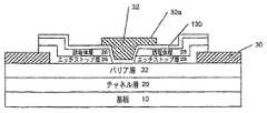
図1Bに示すように、バリア層上にマスク層40を、オーム接点用の開口46をもたらすようにパターニングする。本発明のいくつかの実施形態では、マスク層は、従来のフォトリソグラフィマスク材料でよい。本発明のいくつかの実施形態では、マスク材料は、SiN、SiO2などでよい。図1Cにさらに示すように、例えば、後続のフォトリソグラフィステップおよび蒸着で、オーム性金属をパターニングしてオーム接点材料のパターンを設け、それがアニールされると、オーム接点30がもたらされる。As shown in FIG. 1B, a mask layer 40 is patterned on the barrier layer to provide an
図1Dは、エッチストップ層26および誘電体層28の形成を示す。エッチストップ層26は、バリア層22およびオーム接点30上に形成することができ、エピタキシアル成長させ、かつ/または堆積によって形成することができる。エッチストップ層26は、スパッタAlNでよい。他の諸実施形態では、エッチストップ層26は、SiO2のex−situプラズマ化学気相成長(PECVD)によって形成されたSiO2でよい。一般に、エッチストップ層26は、約50Å〜300Åの厚さを有することができる。誘電体層28は、エッチストップ層26上に形成することができ、堆積によって形成することができる。誘電体層28の材料は、ex−situのPECVDによってエッチストップ層26上に形成したSiN、SiO2、またはSiONを含むことができる。誘電体層28は、エッチストップ層26とは組成が異なる。一般に、誘電体層28は、約500Å〜2000Åの厚さを有することができる。FIG. 1D shows the formation of
図1E〜1Gは、ゲートリセス36の形成を示す。図1Eでは、誘電体層28上に第2のマスクパターン42を形成して、誘電体層28の一部分を露出させるウィンドウを形成するようにパターニングする。本発明のいくつかの実施形態では、第2のマスクパターン42は、従来のフォトリソグラフィマスク材料でよい。本発明のいくつかの実施形態では、マスク材料は、窒化シリコン、二酸化ケイ素などでよい。図1Fに示すように、ゲートリセス36内の少なくとも一部分を含む誘電体層28の露出された部分を、下にあるエッチストップ層26が露出するように除去する。リセス36は、パターニングされたマスク、および誘電体層28を貫通して下にあるエッチストップ層26を露出させるエッチングプロセスを利用して形成することができる。誘電体層28のエッチング速度が、エッチストップ層26のエッチング速度よりも大きいような、特定のエッチングプロセスが選択される。本発明のいくつかの実施形態では、エッチングプロセスは、低損傷エッチングでよい。SiN、SiO2およびSiONなど、誘電体層28の材料向けの低損傷エッチング法の例は、SF6、SF6/O2、CF4、CF4/O2および/または他のフッ化種を使用した誘導結合プラズマ、あるいはプラズマに直流成分のない、または直流成分の少ない、電子サイクロトロン共鳴(ECR)および/またはダウンストリームプラズマエッチングなどのエッチング技法を含む。1E-1G illustrate the formation of the
図1Gに示すように、ゲートリセス36内のエッチストップ層26の露出された部分を除去して、ゲートリセス36内でバリア層22の一部分を露出させる。エッチストップ層26の部分を除去するために、湿式エッチング技法を使用することができる。層を液体薬品中で溶解させることを含む湿式エッチング技法は、与える損傷をより少なくすることができる。それとは対照的に、乾式エッチング技法は一般に、化学的または物理的な衝撃で層をガス状化合物に変換する。エッチストップ層26がスパッタAlNである諸実施形態では、NH4OHなど、水酸化物ベースの現像液を使用することができる。エッチストップ層26がSiO2である他の諸実施形態では、湿式エッチングは、BOEまたはBHFを含んでよい。As shown in FIG. 1G, the exposed portion of the
誘電体層28、乾式エッチング種、エッチストップ層26、および湿式エッチングの適切な組合せを、以下の表1に要約する。 Suitable combinations of

本発明のいくつかの実施形態では、リセス36を、バリア層22内に広がるように形成する。リセス36は、例えば、しきい値電圧、周波数性能などのデバイスの性能特性を調整するために、バリア層22内に広がってよい。リセスは、マスク42および上述のエッチングプロセスを使用して形成することができる。オーム接点30がソース接点およびドレイン接点をもたらす特定の諸実施形態では、リセス、および後にゲート接点32が、ドレイン接点よりもソース接点に近くなるように、リセスをソース接点および/またはドレイン接点の間で中心から外して置くことができる。 In some embodiments of the invention, the
図1Hから分かるように、ゲート接点32がリセス内に形成され、バリア層22の露出された部分に接触する。ゲート接点は「T」ゲートでよく、従来の製造技法を使用して製造することができる。ゲート接点は、ゲート接点32のドレイン側33にある誘電体層28の一部分を覆うフィールドプレート延長部32aを含むことができる。ゲート接点の一部分32bは、文献に記載されているように、より高いクラスの動作を潜在的に可能にするために、ソース側34にある誘電体層28にオーバーラップしてもよい(例えば、その開示を、本明細書に完全に記載されているのと同様に、参照により本明細書に組み込む、2005年3月3日出願の「WIDE BANDGAP TRANSISTORS WITH GATE-SOURCE FIELD PLATES」と題する特許文献23を参照する。)。適切なゲート材料は、バリア層22の組成に依存し得るが、いくつかの実施形態では、Ni、Pt、NiSix、Cu、Pd、Cr、Wおよび/またはWSiNなど、窒化物ベースの半導体材料に対してショットキー接点を形成することができる従来の材料を使用することができる。ゲート接点32とエッチストップ層26または誘電体層28の一方または両方との間に、例えばゲートリセスのエッチングが異方性である結果として、小さな隙間が生じ、その結果、ゲート接点32とエッチストップ層26または誘電体層28の一方または両方との間に、バリア層22の表面が露出し得ることが可能である。この隙間は、意図的に形成してもよい。As can be seen from FIG. 1H, a
また、図1Hから分かるように、オーム接点30上に形成されたエッチストップ層26および誘電体層28の一部分を除去して、オーム接点30へのアクセスを可能にする。これは、ゲートリセスの形成中またはその後に、いつでも行うことができる。エッチストップ層26とバリア層22の間の境界面は、低表面準位密度を有し、バリア層22からエッチストップ層26への電子の注入を防止する高い障壁をもたらすことができる。換言すれば、エッチストップ層26は、良好なパッシベーションをもたらすことができる。 Also, as can be seen in FIG. 1H, a portion of the
パッシベーション層を、図1Hの構造上に形成することもできる。パッシベーション層は、図1Hの構造上にブランケット堆積することができる。本発明のいくつかの実施形態では、パッシベーション層は、窒化シリコン、窒化アルミニウム、二酸化ケイ素、ONO構造および/または酸窒化物でよい。さらに、パッシベーション層は、組成が一様および/または非一様な、単一の層または複数の層とすることができる。 A passivation layer can also be formed on the structure of FIG. 1H. A passivation layer can be blanket deposited on the structure of FIG. 1H. In some embodiments of the present invention, the passivation layer may be silicon nitride, aluminum nitride, silicon dioxide, ONO structure and / or oxynitride. Further, the passivation layer can be a single layer or multiple layers of uniform and / or non-uniform composition.
図2は、本発明の別の諸実施形態によるトランジスタの形成を示す。図2から分かるように、図1Hの構造は、ゲートリセス内を含む構造上に形成された絶縁層130を有することができる。次いで、絶縁層130上にゲート接点32を形成することができる。絶縁層130は、1層または複数層でよく、例えば、SiN、AlN、SiO2および/またはONO構造を含んでよい。したがって、本発明のいくつかの実施形態では、文献に記載されているように絶縁ゲートHEMTを形成することができる(例えば、その開示を本明細書に完全に記載されているのと同様に、参照により本明細書に組み込む、Parikh等の「INSULATING GATE ALGAN/GAN HEMT」と題する特許文献10を参照する)。FIG. 2 illustrates the formation of a transistor according to another embodiment of the invention. As can be seen from FIG. 2, the structure of FIG. 1H can have an
図3は、本発明の別の諸実施形態によるトランジスタの形成を示す。図3から分かるように、構造は、バリア層上に形成された、バリア層22を乾式エッチングから保護するキャップ層24を有することができる。次いで、ゲート接点32の形成が、誘電体層28をキャップ層24まで乾式エッチングすること、および次いで、乾式エッチングによって損傷を受けたキャップ層24の一部分を除去することを含む。ゲート接点32を、キャップ層24上に形成することができる。他の諸実施形態では、キャップ層24の一部分を除去して、バリア層22を露出させ、ゲート接点32をバリア層22の直接上に形成することができる。誘電体層28の乾式エッチングおよびキャップ層24の湿式エッチングを、前述の諸実施形態に従って実施することができる。 FIG. 3 illustrates the formation of a transistor according to another embodiment of the invention. As can be seen from FIG. 3, the structure can have a cap layer 24 formed on the barrier layer that protects the barrier layer 22 from dry etching. The formation of the
バリア層22とは組成が異なるキャップ層24は、III族窒化物でよく、いくつかの実施形態では、GaN、AlGaNおよび/またはInGaNなどのGaNベースの半導体材料でよい。本発明の特定の諸実施形態では、キャップ層はGaNである。キャップ層24とバリア層22がどちらもAlGaNである他の諸実施形態では、キャップ層24の方が低いAlモル分率を有する。キャップ層24がGaN、AlGaNまたはInGaNである諸実施形態では、湿式エッチングが、加熱した水酸化物ベース溶液による湿式エッチングおよび/またはフォトエンハンスド(photo−enhanced)電気化学湿式エッチングでよい。さらに、キャップ層24は、組成および/または厚さが一様および/または非一様な単一の層または複数の層とすることができる。本発明のいくつかの実施形態では、キャップ層24は、文献に記載の傾斜したAlGaN層およびGaN層とすることができる(例えば、その開示を、その全体が記載されているのと同様に、参照により本明細書に組み込む、非特許文献1を参照する。)。例えば、本発明のいくつかの実施形態では、キャップ層24は、SiN層がその上にあるGaN層とすることができる。キャップ層24は、デバイスの上面をチャネルから物理的に遠ざけ、それにより、デバイスの動作に対する表面の影響を低減することができる。 The cap layer 24 having a different composition from the barrier layer 22 may be a group III nitride, and in some embodiments may be a GaN-based semiconductor material such as GaN, AlGaN and / or InGaN. In certain embodiments of the invention, the cap layer is GaN. In other embodiments where both the cap layer 24 and the barrier layer 22 are AlGaN, the cap layer 24 has a lower Al mole fraction. In embodiments where the cap layer 24 is GaN, AlGaN, or InGaN, the wet etch may be a wet etch with a heated hydroxide base solution and / or a photo-enhanced electrochemical wet etch. Further, the cap layer 24 may be a single layer or multiple layers that are uniform and / or non-uniform in composition and / or thickness. In some embodiments of the present invention, the cap layer 24 can be a graded AlGaN layer and a GaN layer as described in the literature (eg, the disclosure is similar to that described in its entirety, (See Non-Patent Document 1, which is incorporated herein by reference). For example, in some embodiments of the present invention, the cap layer 24 can be a GaN layer with a SiN layer thereon. Cap layer 24 can physically move the top surface of the device away from the channel, thereby reducing the effect of the surface on device operation.
キャップ層24は、バリア層22上にブランケット形成することができ、エピタキシアル成長させ、かつ/または堆積により形成することができる。例えば、キャップ層は、GaNキャップ層上へのSiNのin−situ成長によって、あるいはGaNキャップ層の上面上へのSiNまたはSiO2のex−situ PECVDによって、形成することができる。一般に、キャップ層24は、約2nmから約500nmの厚さを有することができる。例えば、SiNおよびGaNからなるキャップ層24は、約300nmの厚さを有することができる。他の諸実施形態では、キャップ層24は、バリア層上22にin−situ成長によって形成させたSiNでよい。本発明のいくつかの実施形態によるキャップ層の例が、Smorchkova等の、「GROUP-III NITRIDE BASED HIGH ELECTRON MOBILITY TRANSISTOR (HEMT) WITH BARRIER/SPACER LAYER」と題する特許文献8に記載されている。The cap layer 24 can be blanket formed on the barrier layer 22 and can be formed by epitaxial growth and / or deposition. For example, the cap layer can be formed by in-situ growth of SiN on the GaN cap layer, or by ex-situ PECVD of SiN or SiO2 on the top surface of the GaN cap layer. In general, the cap layer 24 can have a thickness of about 2 nm to about 500 nm. For example, the cap layer 24 made of SiN and GaN can have a thickness of about 300 nm. In other embodiments, the cap layer 24 may be SiN formed on the barrier layer 22 by in-situ growth. An example of a cap layer according to some embodiments of the present invention is described in Smorchkova et al. In US Pat.
図4は、本発明の別の諸実施形態によるトランジスタの形成を示す。図4から分かるように、構造は、バリア層22上に形成したキャップ層24、キャップ層24上に形成したエッチストップ層26、およびエッチストップ層26上に形成した誘電体層28を有することができる。次いで、ゲート接点32の形成が、誘電体層28をエッチストップ層26まで乾式エッチングすること、および次いで、エッチストップ層26の一部分を除去して、キャップ層24を露出させることを含むことができる。それによって、エッチストップ層26は、キャップ層24を乾式エッチングから保護する。キャップ層24上にゲート接点32を形成することができる。誘電体層28の乾式エッチング、およびエッチストップ層26の湿式エッチングは、前述の諸実施形態に従って実施することができる。キャップ層24は、in−situ成長によって形成させたSiNでよい。 FIG. 4 illustrates the formation of a transistor according to another embodiment of the invention. As can be seen from FIG. 4, the structure has a cap layer 24 formed on the barrier layer 22, an
キャップ層24、エッチストップ層26および/または誘電体層28内に、SiNおよび/またはSiO2を利用する本発明のいくつかの実施形態では、オーム接点30が、SiNおよび/またはSiO2部分を有する層から、オーム接点金属の形成およびパターニング中のずれ交差を可能にするのに十分大きな距離だけ離隔される。オーム接点金属がSiN層および/またはSiO2層に接触する場合、金属が後続の加熱ステップ中にSiN層および/またはSiO2層内に拡散する可能性があり、そのためゲート接点と1つまたは複数のオーム接点30との間に短絡が生ずる恐れがある。In some embodiments of the invention that utilize SiN and / or SiO2 in the cap layer 24,
本発明のいくつかの実施形態によるHEMTデバイスを、文献(例えば、その開示を、本明細書に完全に記載されているのと同様に、参照により本明細書に組み込む、2005年3月15日出願の「GROUP III NITRIDE FIELD EFFECT TRANSISTORS (FETs) CAPABLE OF WITHSTANDING HIGH TEMPERATURE REVERSE BIAS TEST CONDITIONS」と題する特許文献24を参照する。)に記載されたものに類似する高温逆バイアス(HTRB)試験にかけた。試験用のHEMTデバイスは、AlN核形成バッファ層、続いて最後の100Åほどがチャネル層である約6μmのGaN、約0.6nmのAlNおよび約27nmのAlGaNからなるバリア層、スパッタAlNからなるエッチストップ層、ならびに約110nmのSiNからなる誘電体層を含むものであった。ゲート接点を、前述のようにバリア層に対して形成した。 HEMT devices according to some embodiments of the present invention are described in the literature (eg, the disclosure of which is hereby incorporated by reference in its entirety, as if fully disclosed herein, March 15, 2005). A high temperature reverse bias (HTRB) test similar to that described in the application entitled “GROUP III NITRIDE FIELD EFFECT TRANSISTORS (FETs) CAPABLE OF WITHSTANDING HIGH TEMPERATURE REVERSE BIAS TEST CONDITIONS” was applied. The HEMT device for testing consists of an AlN nucleation buffer layer, followed by a barrier layer consisting of about 6 μm GaN, about 0.6 nm AlN and about 27 nm AlGaN, and an etch made of sputtered AlN. It included a stop layer as well as a dielectric layer consisting of about 110 nm SiN. A gate contact was formed to the barrier layer as described above.
HTRB試験を、2フィンガの、周辺部が0.5mmのデバイスの、異なる2つのウェハロットに対して実施した。約−3.0から約−4.0ボルトのピンチオフ電圧を有するHEMTの場合、約28.0ボルトの直流ドレインバイアス、および56ボルトもの電圧に対応する最大ドレインスイングが予測された。ゲート電圧は、約2.0から約3.0Vの間から、約−8から約−10ボルトの間までスイングすることができる。したがって、試験は、56ボルトのドレイン−ソース電圧(VDS)、−8ボルトのゲート−ソース電圧(Vgs)を使用して、140℃の通常動作温度で8時間実施された。結果を以下の表2に列挙する。データは、ウェハAおよびウェハBそれぞれの上にある5つ以上のデバイスの中間データを表す。P1は、Pout@1dB圧縮点を表し、P3は、Pout@3dB圧縮点を表し、IinitはHTRB試験前のゲート漏れ電流を表し、Iendは、HTRB試験後のゲート漏れ電流を表す。表2の最後の列は、HTRBストレス後の、結果として得られるP3出力電力の変化(デルタ)を示す。The HTRB test was performed on two different wafer lots of a 2-finger, 0.5 mm peripheral device. For HEMTs having a pinch-off voltage of about -3.0 to about -4.0 volts, a DC drain bias of about 28.0 volts and a maximum drain swing corresponding to as much as 56 volts were predicted. The gate voltage can swing from between about 2.0 and about 3.0V to between about −8 and about −10 volts. Therefore, the test was conducted for 8 hours at a normal operating temperature of 140 ° C. using a drain-source voltage (VDS ) of 56 volts, a gate-source voltage (Vgs ) of−8 volts. The results are listed in Table 2 below. The data represents intermediate data for five or more devices on each of wafer A and wafer B. P1 represents the Pout @ 1 dB compression point, P3 represents the Pout @ 3 dB compression point, Iinit represents the gate leakage current before the HTRB test, and Iend represents the gate leakage current after the HTRB test. . The last column of Table 2 shows the resulting change in P3 output power (delta) after HTRB stress.
表2の結果は、HTRBストレス後の結果として得られる電力変化が、当業者にとって申し分なく小さくあり得るため、本発明の諸実施形態がHTRBストレス中に破局的に故障し得ないことを示す。具体的には、本発明のいくつかの実施形態によれば、表2の最後の列に示すように、HTRBストレス後に約1dB未満の電力変化を得ることができる。他の諸実施形態では、HTRBストレス後に約0.3dB未満の電力変化を得ることができる。ウェハBに関して、0.150という結果は、HTRBストレス後に任意の測定可能な電力損失がないことを示しているようであるが、実際の増加を示しているようではないことが理解されよう。 The results in Table 2 show that embodiments of the present invention cannot catastrophicly fail during HTRB stress because the resulting power change after HTRB stress can be reasonably small for those skilled in the art. Specifically, according to some embodiments of the present invention, as shown in the last column of Table 2, a power change of less than about 1 dB can be obtained after HTRB stress. In other embodiments, a power change of less than about 0.3 dB can be obtained after HTRB stress. It will be appreciated that for wafer B, a result of 0.150 seems to indicate that there is no any measurable power loss after HTRB stress, but not an actual increase.
本発明の諸実施形態を、特定の操作順序に即して説明してきたが、何らかの順序の修正を行っても、他の操作を含んでも、本発明の教示の恩恵を受けることができる。単一のステップの形で設けられたものとして上記で説明した操作を、複数のステップの形で設けることができ、同様に、複数のステップとして説明した操作を組み合わせて、単一のステップにすることもできる。 While embodiments of the present invention have been described with respect to a particular order of operation, any modification of the order, or including other operations, can benefit from the teachings of the present invention. The operations described above as being provided in the form of a single step can be provided in the form of multiple steps, and similarly, the operations described as multiple steps are combined into a single step. You can also.
以上、本発明の諸実施形態を、本明細書において特定のHEMT構造に関して説明してきたが、本発明は、そうした構造に限定されるものと解釈すべきではない。例えば、追加の層をHEMTデバイス内に含めても、本発明の教示の恩恵を受けることができる。そうした追加の層は、文献に記載のGaNキャップ層を含むことができる(例えば、非特許文献2、または2001年7月12日出願、2002年6月6日公開の、「ALUMINUM GALLIUM NITRIDE/GALLIUM NITRIDE HIGH ELECTRON MOBILITY TRANSISTORS HAVING A GATE CONTACT ON A GALLIUM NITRIDE BASED CAP SEGMENT AND METHODS OF FABRICATING SAME」と題する特許文献6を参照する。それらの開示を、本明細書に完全に記載されているのと同様に、参照により本明細書に組み込む)。いくつかの実施形態では、MISHEMTを製造するために、かつ/または表面を不活性化するために、SiN、ONO構造、または比較的高品質のAlNなどの絶縁層を堆積させることができる。追加の層は、組成が傾斜した1層または複数層の遷移層を含むこともできる。 While embodiments of the present invention have been described herein with reference to particular HEMT structures, the present invention should not be construed as limited to such structures. For example, additional layers can be included in the HEMT device to benefit from the teachings of the present invention. Such additional layers can include the GaN cap layers described in the literature (eg, “ALUMINUM GALLIUM NITRIDE / GALLIUM”, filed July 12, 2001, published June 6, 2002). Reference is made to US Pat. No. 6,057,097 entitled "NITRIDE HIGH ELECTRON MOBILITY TRANSISTORS HAVING A GATE CONTACT ON A GALLIUM NITRIDE BASED CAP SEGMENT AND METHODS OF FABRICATING SAME." , Incorporated herein by reference). In some embodiments, an insulating layer such as SiN, ONO structure, or relatively high quality AlN can be deposited to produce a MISHEMT and / or to deactivate the surface. The additional layers can also include one or more transition layers with graded compositions.
さらに、文献に記載されているように、バリア層22が複数の層を備えることもできる(例えば、その開示を、本明細書に完全に記載されているのと同様に、参照により本明細書に組み込む、Smorchkova等の「GROUP-III NITRIDE BASED HIGH ELECTRON MOBILITY TRANSISTOR (HEMT) WITH BARRIER/SPACER LAYER」と題する特許文献8を参照する。)。したがって、本発明の諸実施形態では、バリア層は単一の層に限定されるものと解釈すべきではなく、例えばGaN、AlGaNおよび/またはAlN層の組合せを有するバリア層を含むことができる。例えば、GaN、AlN構造を、合金散乱を低減または回避するために利用することができる。したがって、本発明の諸実施形態は、窒化物ベースのバリア層を含むことができ、そうした窒化物ベースのバリア層は、AlGaNベースのバリア層、AlNベースのバリア層、およびそれらの組合せを含むことができる。 Further, as described in the literature, the barrier layer 22 may comprise a plurality of layers (eg, the disclosure of which is hereby incorporated by reference as if fully set forth herein). Smorchkova et al., Which is incorporated by reference (see Patent Document 8 entitled “GROUP-III NITRIDE BASED HIGH ELECTRON MOBILITY TRANSISTOR (HEMT) WITH BARRIER / SPACER LAYER”). Thus, in embodiments of the present invention, the barrier layer should not be construed as limited to a single layer, but can include, for example, a barrier layer having a combination of GaN, AlGaN and / or AlN layers. For example, GaN, AlN structures can be utilized to reduce or avoid alloy scattering. Accordingly, embodiments of the present invention can include nitride-based barrier layers, such nitride-based barrier layers including AlGaN-based barrier layers, AlN-based barrier layers, and combinations thereof. Can do.
図面および明細書において、本発明の一般的な諸実施形態が開示されてきた。特定の用語が用いられてきたが、それらは一般的および説明的な意味においてのみ使用されたのであり、限定のためではない。 In the drawings and specification, general embodiments of the invention have been disclosed. Although specific terms have been used, they have been used in a general and descriptive sense only and not for limitation.
Claims (33)
Translated fromJapanese基板と、
前記基板上にある第1の窒化物ベース層と、
前記第1の窒化物ベース層上にあるエッチストップ層と、
前記エッチストップ層上にある誘電体層と、
前記誘電体層を貫通して広がるゲートリセスと、
前記ゲートリセス内のゲート接点と
を備えることを特徴とするIII窒化物ベースのトランジスタ。A III nitride based transistor comprising:
A substrate,
A first nitride base layer on the substrate;
An etch stop layer overlying the first nitride base layer;
A dielectric layer overlying the etch stop layer;
A gate recess extending through the dielectric layer;
A III-nitride based transistor comprising: a gate contact in the gate recess.
をさらに備え、前記ゲート接点は、前記ゲート接点と前記ソース/ドレイン接点との間で前記誘電体層の少なくとも一部分を覆って広がる、フィールドプレート延長部をさらに備えることを特徴とする請求項1に記載のデバイス。A source / drain contact, the gate contact further comprising a field plate extension extending over at least a portion of the dielectric layer between the gate contact and the source / drain contact. The device of claim 1.
基板と、
前記基板上にある窒化物ベースの第1の層であって、GaN、AlGaN、InGaNおよび/またはAlInGaNを含む第1の層と、
前記第1の層上にある窒化物ベースの第2の層であって、GaN、AlN、AlGaN、AlInNおよび/またはAlInGaNを含み、前記第1の層とは異なる第2の層と、
前記第2の層上にある第3の層であって、SiO2、GaN、AlGaNおよび/またはスパッタAlNを含み、前記第2の層とは異なる第3の層と、
前記第3の層上にある第4の層であって、SiN、SiO2および/またはSiONを含み、前記第3の層とは異なる第4の層と、
前記第4の層を貫通して広がるゲートリセスと、
前記ゲートリセス内のゲート接点と
を備えることを特徴とするIII窒化物ベースの高電子移動度トランジスタ(HEMT)。III nitride based high electron mobility transistor (HEMT) comprising:
A substrate,
A nitride-based first layer on the substrate, the first layer comprising GaN, AlGaN, InGaN and / or AlInGaN;
A nitride-based second layer on the first layer, the second layer comprising GaN, AlN, AlGaN, AlInN and / or AlInGaN, and a second layer different from the first layer;
A third layer overlying the second layer, comprising a SiO2 , GaN, AlGaN and / or sputtered AlN, and a third layer different from the second layer;
A fourth layer overlying the third layer, comprising a fourth layer comprising SiN, SiO2 and / or SiON, different from the third layer;
A gate recess extending through the fourth layer;
A III-nitride based high electron mobility transistor (HEMT) comprising: a gate contact in the gate recess.
基板上に第1の窒化物ベース層を形成すること、
前記第1の窒化物ベース層上にエッチストップ層を形成すること、
前記エッチストップ層上に、前記エッチストップ層とは異なる誘電体層を形成すること、
前記誘電体層を前記エッチストップ層まで選択的にエッチングして、前記誘電体層を貫通して前記エッチストップ層まで広がるゲートリセスを形成すること、および
前記ゲートリセス内にゲート接点を形成すること
を含むことを特徴とする方法。A method of manufacturing a III-nitride based transistor comprising:
Forming a first nitride base layer on a substrate;
Forming an etch stop layer on the first nitride base layer;
Forming a dielectric layer different from the etch stop layer on the etch stop layer;
Selectively etching the dielectric layer to the etch stop layer to form a gate recess extending through the dielectric layer to the etch stop layer, and forming a gate contact in the gate recess. A method characterized by that.
前記第1の窒化物ベース層上に、前記エッチストップ層とは異なるキャップ層を形成すること
が実施され、
エッチストップ層を形成することは、前記キャップ層上に、前記キャップ層とは異なるエッチストップ層を形成することを含む
ことを特徴とする請求項25に記載の方法。Between forming the first nitride base layer and forming the etch stop layer, the following:
Forming a cap layer different from the etch stop layer on the first nitride base layer;
26. The method of claim 25, wherein forming an etch stop layer includes forming an etch stop layer on the cap layer that is different from the cap layer.
Applications Claiming Priority (2)
| Application Number | Priority Date | Filing Date | Title |
|---|---|---|---|
| US11/185,398US20070018199A1 (en) | 2005-07-20 | 2005-07-20 | Nitride-based transistors and fabrication methods with an etch stop layer |
| US11/185,398 | 2005-07-20 |
Related Parent Applications (1)
| Application Number | Title | Priority Date | Filing Date |
|---|---|---|---|
| JP2008522820ADivisionJP2009503815A (en) | 2005-07-20 | 2006-07-12 | Nitride-based transistor and manufacturing method using etch stop layer |
Publications (1)
| Publication Number | Publication Date |
|---|---|
| JP2014003301Atrue JP2014003301A (en) | 2014-01-09 |
Family
ID=37114428
Family Applications (2)
| Application Number | Title | Priority Date | Filing Date |
|---|---|---|---|
| JP2008522820APendingJP2009503815A (en) | 2005-07-20 | 2006-07-12 | Nitride-based transistor and manufacturing method using etch stop layer |
| JP2013147350APendingJP2014003301A (en) | 2005-07-20 | 2013-07-16 | Nitride-based transistor and manufacturing method using etch stop layer |
Family Applications Before (1)
| Application Number | Title | Priority Date | Filing Date |
|---|---|---|---|
| JP2008522820APendingJP2009503815A (en) | 2005-07-20 | 2006-07-12 | Nitride-based transistor and manufacturing method using etch stop layer |
Country Status (4)
| Country | Link |
|---|---|
| US (2) | US20070018199A1 (en) |
| EP (2) | EP2479790B1 (en) |
| JP (2) | JP2009503815A (en) |
| WO (1) | WO2007018918A2 (en) |
Cited By (7)
| Publication number | Priority date | Publication date | Assignee | Title |
|---|---|---|---|---|
| KR20200074895A (en) | 2018-12-17 | 2020-06-25 | 나노마테리얼 레버러토리 코., 엘티디. | Manufacturing method of power transistor and power transistor manufactured according to the manufacturing method |
| US11296220B2 (en) | 2020-03-13 | 2022-04-05 | Kabushiki Kaisha Toshiba | Semiconductor device, power supply circuit, and computer |
| JP2023015378A (en)* | 2019-12-16 | 2023-01-31 | 株式会社東芝 | semiconductor equipment |
| KR20230152545A (en) | 2022-04-27 | 2023-11-03 | 나노마테리얼 레버러토리 코., 엘티디. | Power device |
| JP2024528836A (en)* | 2021-08-30 | 2024-08-01 | 華為技術有限公司 | Gallium nitride element, method for manufacturing a gallium nitride element, and electronic device |
| US12349386B2 (en) | 2021-01-20 | 2025-07-01 | Kabushiki Kaisha Toshiba | Semiconductor device and method for manufacturing the same |
| US12439665B2 (en) | 2022-06-30 | 2025-10-07 | Fujitsu Limited | Semiconductor device, method for manufacturing semiconductor device, and electronic device |
Families Citing this family (183)
| Publication number | Priority date | Publication date | Assignee | Title |
|---|---|---|---|---|
| US7112860B2 (en) | 2003-03-03 | 2006-09-26 | Cree, Inc. | Integrated nitride-based acoustic wave devices and methods of fabricating integrated nitride-based acoustic wave devices |
| US7898047B2 (en)* | 2003-03-03 | 2011-03-01 | Samsung Electronics Co., Ltd. | Integrated nitride and silicon carbide-based devices and methods of fabricating integrated nitride-based devices |
| US7709859B2 (en) | 2004-11-23 | 2010-05-04 | Cree, Inc. | Cap layers including aluminum nitride for nitride-based transistors |
| WO2006080109A1 (en)* | 2005-01-25 | 2006-08-03 | Fujitsu Limited | Semiconductor device provided with mis structure and method for manufacturing the same |
| US8168000B2 (en)* | 2005-06-15 | 2012-05-01 | International Rectifier Corporation | III-nitride semiconductor device fabrication |
| US7855401B2 (en)* | 2005-06-29 | 2010-12-21 | Cree, Inc. | Passivation of wide band-gap based semiconductor devices with hydrogen-free sputtered nitrides |
| US8183595B2 (en)* | 2005-07-29 | 2012-05-22 | International Rectifier Corporation | Normally off III-nitride semiconductor device having a programmable gate |
| US9608102B2 (en)* | 2005-12-02 | 2017-03-28 | Infineon Technologies Americas Corp. | Gallium nitride material devices and associated methods |
| US7592211B2 (en) | 2006-01-17 | 2009-09-22 | Cree, Inc. | Methods of fabricating transistors including supported gate electrodes |
| US7709269B2 (en)* | 2006-01-17 | 2010-05-04 | Cree, Inc. | Methods of fabricating transistors including dielectrically-supported gate electrodes |
| US8338861B2 (en)* | 2007-01-10 | 2012-12-25 | International Rectifier Corporation | III-nitride semiconductor device with stepped gate trench and process for its manufacture |
| US8987784B2 (en)* | 2007-01-10 | 2015-03-24 | International Rectifier Corporation | Active area shaping of III-nitride devices utilizing multiple dielectric materials |
| US9525052B2 (en)* | 2007-01-10 | 2016-12-20 | Infineon Technologies Americas Corp. | Active area shaping of III-nitride devices utilizing a field plate defined by a dielectric body |
| US8946778B2 (en) | 2007-01-10 | 2015-02-03 | International Rectifier Corporation | Active area shaping of III-nitride devices utilizing steps of source-side and drain-side field plates |
| US9318592B2 (en)* | 2007-01-10 | 2016-04-19 | Infineon Technologies Americas Corp. | Active area shaping of III-nitride devices utilizing a source-side field plate and a wider drain-side field plate |
| US7973304B2 (en)* | 2007-02-06 | 2011-07-05 | International Rectifier Corporation | III-nitride semiconductor device |
| JP5186776B2 (en)* | 2007-02-22 | 2013-04-24 | 富士通株式会社 | Semiconductor device and manufacturing method thereof |
| US7875537B2 (en)* | 2007-08-29 | 2011-01-25 | Cree, Inc. | High temperature ion implantation of nitride based HEMTs |
| US7795642B2 (en) | 2007-09-14 | 2010-09-14 | Transphorm, Inc. | III-nitride devices with recessed gates |
| US7915643B2 (en) | 2007-09-17 | 2011-03-29 | Transphorm Inc. | Enhancement mode gallium nitride power devices |
| US20090072269A1 (en)* | 2007-09-17 | 2009-03-19 | Chang Soo Suh | Gallium nitride diodes and integrated components |
| FR2922045B1 (en)* | 2007-10-05 | 2011-07-15 | Thales Sa | HIGH ELECTRONIC MOBILITY TRANSISTOR AND METHOD FOR MANUFACTURING THE SAME |
| US8431962B2 (en)* | 2007-12-07 | 2013-04-30 | Northrop Grumman Systems Corporation | Composite passivation process for nitride FET |
| US7750370B2 (en)* | 2007-12-20 | 2010-07-06 | Northrop Grumman Space & Mission Systems Corp. | High electron mobility transistor having self-aligned miniature field mitigating plate on a protective dielectric layer |
| JP5092740B2 (en)* | 2007-12-28 | 2012-12-05 | 住友電気工業株式会社 | Manufacturing method of semiconductor device |
| JP5276849B2 (en)* | 2008-01-09 | 2013-08-28 | 新日本無線株式会社 | Manufacturing method of nitride semiconductor device |
| US7795691B2 (en)* | 2008-01-25 | 2010-09-14 | Cree, Inc. | Semiconductor transistor with P type re-grown channel layer |
| US8519438B2 (en) | 2008-04-23 | 2013-08-27 | Transphorm Inc. | Enhancement mode III-N HEMTs |
| US8289065B2 (en) | 2008-09-23 | 2012-10-16 | Transphorm Inc. | Inductive load power switching circuits |
| JP2010098047A (en)* | 2008-10-15 | 2010-04-30 | Sanken Electric Co Ltd | Nitride semiconductor device |
| JP2010118556A (en)* | 2008-11-13 | 2010-05-27 | Furukawa Electric Co Ltd:The | Semiconductor device and its manufacturing method |
| US7898004B2 (en) | 2008-12-10 | 2011-03-01 | Transphorm Inc. | Semiconductor heterostructure diodes |
| JP5487613B2 (en)* | 2008-12-19 | 2014-05-07 | 富士通株式会社 | Compound semiconductor device and manufacturing method thereof |
| JP5691138B2 (en)* | 2009-04-28 | 2015-04-01 | 日亜化学工業株式会社 | Field effect transistor and manufacturing method thereof |
| US8742459B2 (en) | 2009-05-14 | 2014-06-03 | Transphorm Inc. | High voltage III-nitride semiconductor devices |
| DE102009028918B4 (en) | 2009-08-26 | 2014-11-06 | Fraunhofer-Gesellschaft zur Förderung der angewandten Forschung e.V. | Semiconductor device, method for determining the structure of a transistor and base station for a mobile radio network |
| US8390000B2 (en)* | 2009-08-28 | 2013-03-05 | Transphorm Inc. | Semiconductor devices with field plates |
| JP5537555B2 (en)* | 2009-09-29 | 2014-07-02 | 株式会社東芝 | Semiconductor device |
| JP2011082216A (en)* | 2009-10-02 | 2011-04-21 | Fujitsu Ltd | Compound semiconductor device and method for manufacturing the same |
| TWI426565B (en)* | 2009-10-15 | 2014-02-11 | Au Optronics Corp | Rework method for display panel and gate insulating layer of thin film transistor |
| JP5625336B2 (en)* | 2009-11-30 | 2014-11-19 | サンケン電気株式会社 | Semiconductor device |
| KR101274713B1 (en)* | 2009-12-07 | 2013-06-12 | 엘지디스플레이 주식회사 | Method of fabricaitng cliche and method of fabricating thin film pattern using the cliche |
| US8258543B2 (en)* | 2009-12-07 | 2012-09-04 | Intel Corporation | Quantum-well-based semiconductor devices |
| JP2011124246A (en)* | 2009-12-08 | 2011-06-23 | Mitsubishi Electric Corp | Heterojunction field effect transistor and method of manufacturing the same |
| US8389977B2 (en) | 2009-12-10 | 2013-03-05 | Transphorm Inc. | Reverse side engineered III-nitride devices |
| US9378965B2 (en)* | 2009-12-10 | 2016-06-28 | Infineon Technologies Americas Corp. | Highly conductive source/drain contacts in III-nitride transistors |
| US8936976B2 (en)* | 2009-12-23 | 2015-01-20 | Intel Corporation | Conductivity improvements for III-V semiconductor devices |
| US8624260B2 (en) | 2010-01-30 | 2014-01-07 | National Semiconductor Corporation | Enhancement-mode GaN MOSFET with low leakage current and improved reliability |
| US8357571B2 (en)* | 2010-09-10 | 2013-01-22 | Cree, Inc. | Methods of forming semiconductor contacts |
| JP5781292B2 (en)* | 2010-11-16 | 2015-09-16 | ローム株式会社 | Nitride semiconductor device and nitride semiconductor package |
| JP5724339B2 (en)* | 2010-12-03 | 2015-05-27 | 富士通株式会社 | Compound semiconductor device and manufacturing method thereof |
| KR101736914B1 (en)* | 2010-12-06 | 2017-05-19 | 한국전자통신연구원 | Method of manufacturing high frequency device structures |
| US8742460B2 (en)* | 2010-12-15 | 2014-06-03 | Transphorm Inc. | Transistors with isolation regions |
| US8643062B2 (en) | 2011-02-02 | 2014-02-04 | Transphorm Inc. | III-N device structures and methods |
| US8772842B2 (en) | 2011-03-04 | 2014-07-08 | Transphorm, Inc. | Semiconductor diodes with low reverse bias currents |
| US8716141B2 (en) | 2011-03-04 | 2014-05-06 | Transphorm Inc. | Electrode configurations for semiconductor devices |
| US9024357B2 (en)* | 2011-04-15 | 2015-05-05 | Stmicroelectronics S.R.L. | Method for manufacturing a HEMT transistor and corresponding HEMT transistor |
| KR20120120828A (en)* | 2011-04-25 | 2012-11-02 | 삼성전기주식회사 | Nitride semiconductor device and manufacturing method thereof |
| CN102201334B (en)* | 2011-05-23 | 2013-03-20 | 中国科学院微电子研究所 | Method for manufacturing U-shaped grid pin T-shaped grid structure |
| CN103548127B (en)* | 2011-06-13 | 2016-12-07 | 松下知识产权经营株式会社 | Semiconductor device and manufacturing method thereof |
| US9070758B2 (en) | 2011-06-20 | 2015-06-30 | Imec | CMOS compatible method for manufacturing a HEMT device and the HEMT device thereof |
| GB201112330D0 (en)* | 2011-07-18 | 2011-08-31 | Epigan Nv | Method for growing III-V epitaxial layers and semiconductor structure |
| CN102299175B (en)* | 2011-08-29 | 2013-07-17 | 中国电子科技集团公司第十三研究所 | Buried layer structure of InAIN/GaN heterogenous-junction active-area and activation method thereof |
| CN102290439B (en)* | 2011-08-29 | 2013-02-20 | 中国电子科技集团公司第十三研究所 | InAIN/ GaN HEM device with etch stop layer |
| US8901604B2 (en) | 2011-09-06 | 2014-12-02 | Transphorm Inc. | Semiconductor devices with guard rings |
| US9257547B2 (en) | 2011-09-13 | 2016-02-09 | Transphorm Inc. | III-N device structures having a non-insulating substrate |
| JP5765171B2 (en)* | 2011-09-29 | 2015-08-19 | 富士通株式会社 | Method for manufacturing compound semiconductor device |
| US8598937B2 (en) | 2011-10-07 | 2013-12-03 | Transphorm Inc. | High power semiconductor electronic components with increased reliability |
| US9018677B2 (en)* | 2011-10-11 | 2015-04-28 | Taiwan Semiconductor Manufacturing Company, Ltd. | Semiconductor structure and method of forming the same |
| US8946771B2 (en)* | 2011-11-09 | 2015-02-03 | Taiwan Semiconductor Manufacturing Co., Ltd. | Gallium nitride semiconductor devices and method making thereof |
| US8723226B2 (en)* | 2011-11-22 | 2014-05-13 | Texas Instruments Incorporated | Manufacturable enhancement-mode group III-N HEMT with a reverse polarization cap |
| JP2013125918A (en)* | 2011-12-16 | 2013-06-24 | Sumitomo Electric Ind Ltd | Semiconductor device |
| JP2013131650A (en)* | 2011-12-21 | 2013-07-04 | Fujitsu Ltd | Semiconductor device and method of manufacturing the same |
| CN103187451B (en)* | 2012-01-03 | 2017-04-05 | 管炜 | Thin film transistor (TFT) |
| US9165766B2 (en) | 2012-02-03 | 2015-10-20 | Transphorm Inc. | Buffer layer structures suited for III-nitride devices with foreign substrates |
| US8860088B2 (en)* | 2012-02-23 | 2014-10-14 | Taiwan Semiconductor Manufacturing Company, Ltd. | Semiconductor structure and method of forming the same |
| US8941148B2 (en)* | 2012-03-06 | 2015-01-27 | Infineon Technologies Austria Ag | Semiconductor device and method |
| WO2013155108A1 (en) | 2012-04-09 | 2013-10-17 | Transphorm Inc. | N-polar iii-nitride transistors |
| US9443941B2 (en)* | 2012-06-04 | 2016-09-13 | Infineon Technologies Austria Ag | Compound semiconductor transistor with self aligned gate |
| US20140151712A1 (en)* | 2012-06-07 | 2014-06-05 | Iqe, Kc, Llc | Enhancement-mode high electron mobility transistor structure and method of making same |
| JP2013258251A (en)* | 2012-06-12 | 2013-12-26 | Sumitomo Electric Ind Ltd | Schottky barrier diode and method for manufacturing the same |
| US10522670B2 (en) | 2012-06-26 | 2019-12-31 | Nxp Usa, Inc. | Semiconductor device with selectively etched surface passivation |
| US8946776B2 (en) | 2012-06-26 | 2015-02-03 | Freescale Semiconductor, Inc. | Semiconductor device with selectively etched surface passivation |
| US9111868B2 (en)* | 2012-06-26 | 2015-08-18 | Freescale Semiconductor, Inc. | Semiconductor device with selectively etched surface passivation |
| US10825924B2 (en) | 2012-06-26 | 2020-11-03 | Nxp Usa, Inc. | Semiconductor device with selectively etched surface passivation |
| US9184275B2 (en) | 2012-06-27 | 2015-11-10 | Transphorm Inc. | Semiconductor devices with integrated hole collectors |
| US9991399B2 (en) | 2012-10-04 | 2018-06-05 | Cree, Inc. | Passivation structure for semiconductor devices |
| US9812338B2 (en) | 2013-03-14 | 2017-11-07 | Cree, Inc. | Encapsulation of advanced devices using novel PECVD and ALD schemes |
| US8994073B2 (en) | 2012-10-04 | 2015-03-31 | Cree, Inc. | Hydrogen mitigation schemes in the passivation of advanced devices |
| JP6486828B2 (en)* | 2012-11-16 | 2019-03-20 | マサチューセッツ インスティテュート オブ テクノロジー | Etching technology for semiconductor structure and recess formation |
| CN103022136B (en)* | 2012-12-26 | 2015-09-30 | 电子科技大学 | A kind of MOS transistor of T-shaped grid structure |
| CN103050399B (en)* | 2012-12-28 | 2015-11-25 | 杭州士兰集成电路有限公司 | There is diode and the manufacture method thereof of three layers of dielectric passivation structure |
| US9525054B2 (en)* | 2013-01-04 | 2016-12-20 | Taiwan Semiconductor Manufacturing Company, Ltd. | High electron mobility transistor and method of forming the same |
| JP2014138111A (en)* | 2013-01-17 | 2014-07-28 | Fujitsu Ltd | Semiconductor device and manufacturing method of the same, power supply device and high-frequency amplifier |
| CN105164811B (en) | 2013-02-15 | 2018-08-31 | 创世舫电子有限公司 | Electrode of semiconductor devices and forming method thereof |
| US8946779B2 (en) | 2013-02-26 | 2015-02-03 | Freescale Semiconductor, Inc. | MISHFET and Schottky device integration |
| US9343561B2 (en)* | 2013-03-13 | 2016-05-17 | Cree, Inc. | Semiconductor device with self-aligned ohmic contacts |
| US9087718B2 (en) | 2013-03-13 | 2015-07-21 | Transphorm Inc. | Enhancement-mode III-nitride devices |
| US8969927B2 (en) | 2013-03-13 | 2015-03-03 | Cree, Inc. | Gate contact for a semiconductor device and methods of fabrication thereof |
| US9070705B2 (en)* | 2013-03-15 | 2015-06-30 | Semiconductor Components Industries, Llc | HEMT semiconductor device and a process of forming the same |
| US9245992B2 (en) | 2013-03-15 | 2016-01-26 | Transphorm Inc. | Carbon doping semiconductor devices |
| US9755059B2 (en) | 2013-06-09 | 2017-09-05 | Cree, Inc. | Cascode structures with GaN cap layers |
| US9443938B2 (en) | 2013-07-19 | 2016-09-13 | Transphorm Inc. | III-nitride transistor including a p-type depleting layer |
| US9564330B2 (en)* | 2013-08-01 | 2017-02-07 | Taiwan Semiconductor Manufacturing Co., Ltd. | Normally-off enhancement-mode MISFET |
| US9263569B2 (en)* | 2013-08-05 | 2016-02-16 | Taiwan Semiconductor Manufacturing Company, Ltd. | MISFET device and method of forming the same |
| CN104810264B (en)* | 2014-01-26 | 2017-12-01 | 国家电网公司 | A kind of SiC terminal structure preparation methods based on ONO structure |
| EP2930754A1 (en)* | 2014-04-11 | 2015-10-14 | Nxp B.V. | Semiconductor device |
| US9318593B2 (en) | 2014-07-21 | 2016-04-19 | Transphorm Inc. | Forming enhancement mode III-nitride devices |
| CN104347700A (en)* | 2014-08-20 | 2015-02-11 | 佛山芯光半导体有限公司 | GaN(gallium nitride)-based concave grating enhanced HEMT (high electron mobility transistor) device |
| CN104241400B (en)* | 2014-09-05 | 2017-03-08 | 苏州捷芯威半导体有限公司 | Field-effect diode and preparation method thereof |
| CN104465746B (en)* | 2014-09-28 | 2018-08-10 | 苏州能讯高能半导体有限公司 | A kind of HEMT device and its manufacturing method |
| JP6292104B2 (en)* | 2014-11-17 | 2018-03-14 | 三菱電機株式会社 | Manufacturing method of nitride semiconductor device |
| US9419083B2 (en) | 2014-11-21 | 2016-08-16 | Raytheon Company | Semiconductor structures having a gate field plate and methods for forming such structure |
| KR101672396B1 (en)* | 2014-11-25 | 2016-11-04 | (재)한국나노기술원 | Quaternary nitride semiconductor power device and manufacturing method thereof |
| US10036774B2 (en)* | 2014-12-04 | 2018-07-31 | Arm Limited | Integrated circuit device comprising environment-hardened die and less-environment-hardened die |
| US9536966B2 (en) | 2014-12-16 | 2017-01-03 | Transphorm Inc. | Gate structures for III-N devices |
| US9536967B2 (en) | 2014-12-16 | 2017-01-03 | Transphorm Inc. | Recessed ohmic contacts in a III-N device |
| JP6401053B2 (en)* | 2014-12-26 | 2018-10-03 | ルネサスエレクトロニクス株式会社 | Semiconductor device and manufacturing method of semiconductor device |
| JP2016171162A (en)* | 2015-03-12 | 2016-09-23 | 株式会社東芝 | Semiconductor device |
| CN105185841B (en)* | 2015-04-07 | 2018-06-12 | 苏州捷芯威半导体有限公司 | A kind of field-effect diode and preparation method thereof |
| US9614069B1 (en) | 2015-04-10 | 2017-04-04 | Cambridge Electronics, Inc. | III-Nitride semiconductors with recess regions and methods of manufacture |
| US9876082B2 (en)* | 2015-04-30 | 2018-01-23 | Macom Technology Solutions Holdings, Inc. | Transistor with hole barrier layer |
| US9941384B2 (en)* | 2015-08-29 | 2018-04-10 | Taiwan Semiconductor Manufacturing Co., Ltd. | Semiconductor device and method for fabricating the same |
| US9871067B2 (en)* | 2015-11-17 | 2018-01-16 | Taiwan Semiconductor Manufacturing Co., Ltd. | Infrared image sensor component |
| US11322599B2 (en) | 2016-01-15 | 2022-05-03 | Transphorm Technology, Inc. | Enhancement mode III-nitride devices having an Al1-xSixO gate insulator |
| US9941398B2 (en)* | 2016-03-17 | 2018-04-10 | Taiwan Semiconductor Manufacturing Company Ltd. | High-electron-mobility transistor (HEMT) capable of protecting a III-V compound layer |
| US20170301780A1 (en) | 2016-04-15 | 2017-10-19 | Macom Technology Solutions Holdings, Inc. | High-voltage gan high electron mobility transistors with reduced leakage current |
| US10651317B2 (en) | 2016-04-15 | 2020-05-12 | Macom Technology Solutions Holdings, Inc. | High-voltage lateral GaN-on-silicon Schottky diode |
| EP3459118A4 (en)* | 2016-05-17 | 2020-01-15 | The Government Of The United States Of America As The Secretary of The Navy | PASSIVATION BY CHEMICAL VAPOR DEPOSIT ASSISTED BY PLASMA WITHOUT DAMAGE TO HIGH ELECTRONIC MOBILITY TRANSISTORS IN ALGAN / GAN |
| TWI762486B (en) | 2016-05-31 | 2022-05-01 | 美商創世舫科技有限公司 | Iii-nitride devices including a graded depleting layer |
| CN105977147B (en)* | 2016-07-29 | 2020-03-31 | 中国电子科技集团公司第十三研究所 | Damage-free self-termination etching method for nano-gate preparation |
| RU2624600C1 (en)* | 2016-10-07 | 2017-07-04 | Федеральное государственное бюджетное учреждение науки Институт сверхвысокочастотной полупроводниковой электроники Российской академии наук (ИСВЧПЭ РАН) | Manufacturing method of t-shaped gate |
| US10332840B2 (en) | 2017-03-21 | 2019-06-25 | Macronix International Co., Ltd. | Semiconductor device with physically unclonable function (PUF) and apparatus including the same |
| CN107170821B (en)* | 2017-03-29 | 2020-04-14 | 西安电子科技大学 | Floating type drain field plate current aperture device and method of making the same |
| CN107424919A (en)* | 2017-05-12 | 2017-12-01 | 中国电子科技集团公司第十三研究所 | A kind of low Damage Medium grid and preparation method thereof |
| CN107170809B (en)* | 2017-06-16 | 2023-12-12 | 北京星云联众科技有限公司 | GaNHEMT device based on self-alignment process and manufacturing method thereof |
| JP6472839B2 (en)* | 2017-06-20 | 2019-02-20 | ルネサスエレクトロニクス株式会社 | Semiconductor device |
| JP2017208556A (en)* | 2017-06-27 | 2017-11-24 | 株式会社東芝 | Semiconductor device |
| WO2019005081A1 (en)* | 2017-06-29 | 2019-01-03 | Intel Corporation | Group iii-nitride transistor structure with embedded diode |
| WO2019066972A1 (en) | 2017-09-29 | 2019-04-04 | Intel Corporation | Group iii-nitride schottky diode |
| DE112017007912T5 (en) | 2017-09-29 | 2020-07-02 | Intel Corporation | GROUP III NITRIDE ANTENNA DIODE |
| US10134596B1 (en)* | 2017-11-21 | 2018-11-20 | Texas Instruments Incorporated | Recessed solid state apparatuses |
| CN108133961A (en)* | 2017-12-20 | 2018-06-08 | 成都海威华芯科技有限公司 | A kind of GaN_HEMT device preparation methods based on aluminum nitride barrier layers |
| RU2686863C1 (en)* | 2017-12-27 | 2019-05-06 | Федеральное государственное бюджетное образовательное учреждение высшего образования "Томский государственный университет систем управления и радиоэлектроники" (ТУСУР) | Method of forming t-shaped gate |
| CN108376706A (en)* | 2018-01-11 | 2018-08-07 | 北京华碳科技有限责任公司 | A kind of GaN base HEMT device and its manufacturing method |
| US11233047B2 (en) | 2018-01-19 | 2022-01-25 | Macom Technology Solutions Holdings, Inc. | Heterolithic microwave integrated circuits including gallium-nitride devices on highly doped regions of intrinsic silicon |
| US11056483B2 (en) | 2018-01-19 | 2021-07-06 | Macom Technology Solutions Holdings, Inc. | Heterolithic microwave integrated circuits including gallium-nitride devices on intrinsic semiconductor |
| US10950598B2 (en) | 2018-01-19 | 2021-03-16 | Macom Technology Solutions Holdings, Inc. | Heterolithic microwave integrated circuits including gallium-nitride devices formed on highly doped semiconductor |
| US10566200B2 (en)* | 2018-04-03 | 2020-02-18 | Texas Instruments Incorporated | Method of fabricating transistors, including ambient oxidizing after etchings into barrier layers and anti-reflecting coatings |
| JP7143660B2 (en)* | 2018-07-18 | 2022-09-29 | サンケン電気株式会社 | semiconductor equipment |
| CN109308999B (en)* | 2018-09-29 | 2022-03-29 | 大连芯冠科技有限公司 | Method for preparing power device multi-field plate by selective etching |
| TWI692867B (en)* | 2018-10-04 | 2020-05-01 | 新唐科技股份有限公司 | High electron mobility transistor device and manufacturing method thereof |
| US10964803B2 (en) | 2018-11-19 | 2021-03-30 | Texas Instruments Incorporated | Gallium nitride transistor with a doped region |
| US10937873B2 (en) | 2019-01-03 | 2021-03-02 | Cree, Inc. | High electron mobility transistors having improved drain current drift and/or leakage current performance |
| WO2020215322A1 (en)* | 2019-04-26 | 2020-10-29 | 苏州晶湛半导体有限公司 | Semiconductor structure and preparation method therefor |
| CN110289310A (en)* | 2019-06-29 | 2019-09-27 | 厦门市三安集成电路有限公司 | Transistor, gate structure and fabrication method thereof |
| CN112750904B (en) | 2019-10-30 | 2024-01-02 | 联华电子股份有限公司 | Semiconductor element with stress relaxation layer |
| CN110808211A (en)* | 2019-11-08 | 2020-02-18 | 中国电子科技集团公司第十三研究所 | Slanted gate structure gallium oxide field effect transistor and preparation method thereof |
| US11658233B2 (en) | 2019-11-19 | 2023-05-23 | Wolfspeed, Inc. | Semiconductors with improved thermal budget and process of making semiconductors with improved thermal budget |
| CN110942990A (en)* | 2019-12-16 | 2020-03-31 | 成都大学 | AlGaN/GaN HEMT heat management method |
| WO2021195506A1 (en) | 2020-03-26 | 2021-09-30 | Macom Technology Solutions Holdings, Inc. | Microwave integrated circuits including gallium-nitride devices on silicon |
| EP3905335A1 (en)* | 2020-04-28 | 2021-11-03 | Infineon Technologies AG | Group iii nitride-based transistor device |
| CN112038227A (en)* | 2020-08-12 | 2020-12-04 | 深圳市汇芯通信技术有限公司 | Non-destructive preparation method of gate and HEMT based on the preparation method |
| TWI811562B (en)* | 2020-08-18 | 2023-08-11 | 新唐科技股份有限公司 | Manufacturing method of semiconductor device |
| CN114122126A (en)* | 2020-08-27 | 2022-03-01 | 世界先进积体电路股份有限公司 | Semiconductor structure |
| WO2022087869A1 (en)* | 2020-10-28 | 2022-05-05 | Innoscience (Suzhou) Technology Co., Ltd. | Semiconductor device and fabrication method thereof |
| US12040368B2 (en)* | 2020-11-30 | 2024-07-16 | Innoscience (suzhou) Semiconductor Co., Ltd. | Semiconductor device and manufacturing method thereof |
| CN114582970A (en) | 2020-12-01 | 2022-06-03 | 联华电子股份有限公司 | Semiconductor device and method for fabricating the same |
| US11450764B2 (en)* | 2020-12-29 | 2022-09-20 | Vanguard International Semiconductor Corporation | Semiconductor device and method of forming the same |
| JP7564753B2 (en) | 2021-04-15 | 2024-10-09 | 株式会社東芝 | Semiconductor Device |
| US12218202B2 (en)* | 2021-09-16 | 2025-02-04 | Wolfspeed, Inc. | Semiconductor device incorporating a substrate recess |
| CN114361016B (en)* | 2021-11-24 | 2025-10-03 | 西安电子科技大学 | A low-power radio frequency power device and its manufacturing method |
| JP2023132608A (en)* | 2022-03-11 | 2023-09-22 | 住友電気工業株式会社 | Method for manufacturing semiconductor device |
| US12419070B2 (en)* | 2022-04-27 | 2025-09-16 | United Microelectronics Corp. | Semiconductor device including III-V compound semiconductor layer and manufacturing method thereof |
| US12369380B2 (en) | 2022-05-03 | 2025-07-22 | Nxp Usa, Inc. | Transistor with dielectric spacers and field plate and method of fabrication therefor |
| US12266713B2 (en) | 2022-05-03 | 2025-04-01 | Nxp Usa, Inc. | Transistor with dielectric spacers and method of fabrication therefor |
| CN117238855A (en)* | 2022-06-07 | 2023-12-15 | 华为技术有限公司 | Semiconductor device and preparation method thereof |
| TWI842078B (en) | 2022-09-02 | 2024-05-11 | 力晶積成電子製造股份有限公司 | High electron mobility transistor device and manufacturing method thereof |
| CN117954501A (en)* | 2022-10-18 | 2024-04-30 | 联华电子股份有限公司 | Field effect transistor and method for manufacturing the same |
| US20240243194A1 (en)* | 2023-01-17 | 2024-07-18 | Vanguard International Semiconductor Corporation | High electron mobility transistor structure and fabrication method thereof |
| US20240363745A1 (en)* | 2023-04-27 | 2024-10-31 | Wisconsin Alumni Research Foundation | High-frequency group iii-nitride-based high electron mobility transistors with high-aluminum concentration barriers and recessed gates |
| US20250006818A1 (en)* | 2023-06-29 | 2025-01-02 | Nxp Usa, Inc. | Transistors with dielectric spacers and methods of fabrication thereof |
| CN118039687A (en)* | 2024-01-24 | 2024-05-14 | 湖北九峰山实验室 | GaN-based device with low contact resistance and preparation method thereof |
Citations (4)
| Publication number | Priority date | Publication date | Assignee | Title |
|---|---|---|---|---|
| JP2002093819A (en)* | 2000-09-11 | 2002-03-29 | Ricoh Co Ltd | Semiconductor device and its manufacturing method |
| JP2004200248A (en)* | 2002-12-16 | 2004-07-15 | Nec Corp | Field effect transistor |
| JP2005136002A (en)* | 2003-10-28 | 2005-05-26 | Oki Electric Ind Co Ltd | Mask for photoelectrochemical etching, method for forming the same, and method for manufacturing a semiconductor device using the mask for photoelectrochemical etching |
| WO2005057624A2 (en)* | 2003-12-05 | 2005-06-23 | International Rectifier Corporation | Iii-nitride device passivation and method |
Family Cites Families (43)
| Publication number | Priority date | Publication date | Assignee | Title |
|---|---|---|---|---|
| JPS59127871A (en)* | 1983-01-13 | 1984-07-23 | Nec Corp | Manufacturing method of semiconductor device |
| US4866005A (en)* | 1987-10-26 | 1989-09-12 | North Carolina State University | Sublimation of silicon carbide to produce large, device quality single crystals of silicon carbide |
| US4946547A (en) | 1989-10-13 | 1990-08-07 | Cree Research, Inc. | Method of preparing silicon carbide surfaces for crystal growth |
| DE58909785D1 (en)* | 1989-11-28 | 1997-04-10 | Siemens Ag | Semiconductor wafer with doped scratch frame |
| US5210051A (en)* | 1990-03-27 | 1993-05-11 | Cree Research, Inc. | High efficiency light emitting diodes from bipolar gallium nitride |
| US5292501A (en)* | 1990-06-25 | 1994-03-08 | Degenhardt Charles R | Use of a carboxy-substituted polymer to inhibit plaque formation without tooth staining |
| JPH0492439A (en)* | 1990-08-08 | 1992-03-25 | Hitachi Ltd | Method for manufacturing semiconductor integrated circuit device |
| US5200022A (en)* | 1990-10-03 | 1993-04-06 | Cree Research, Inc. | Method of improving mechanically prepared substrate surfaces of alpha silicon carbide for deposition of beta silicon carbide thereon and resulting product |
| US5192987A (en)* | 1991-05-17 | 1993-03-09 | Apa Optics, Inc. | High electron mobility transistor with GaN/Alx Ga1-x N heterojunctions |
| US5270554A (en)* | 1991-06-14 | 1993-12-14 | Cree Research, Inc. | High power high frequency metal-semiconductor field-effect transistor formed in silicon carbide |
| JPH0582560A (en)* | 1991-09-20 | 1993-04-02 | Sony Corp | Method for manufacturing field effect transistor |
| US5393993A (en)* | 1993-12-13 | 1995-02-28 | Cree Research, Inc. | Buffer structure between silicon carbide and gallium nitride and resulting semiconductor devices |
| JPH07211730A (en)* | 1994-01-20 | 1995-08-11 | Hitachi Ltd | Semiconductor device and manufacturing method thereof |
| US5484740A (en)* | 1994-06-06 | 1996-01-16 | Motorola, Inc. | Method of manufacturing a III-V semiconductor gate structure |
| US5523589A (en)* | 1994-09-20 | 1996-06-04 | Cree Research, Inc. | Vertical geometry light emitting diode with group III nitride active layer and extended lifetime |
| JPH092439A (en) | 1995-06-14 | 1997-01-07 | Lion Corp | Hot stamping method and apparatus |
| JP2904167B2 (en)* | 1996-12-18 | 1999-06-14 | 日本電気株式会社 | Method for manufacturing semiconductor device |
| US6316793B1 (en)* | 1998-06-12 | 2001-11-13 | Cree, Inc. | Nitride based transistors on semi-insulating silicon carbide substrates |
| JP3180776B2 (en)* | 1998-09-22 | 2001-06-25 | 日本電気株式会社 | Field-effect transistor |
| US6218680B1 (en)* | 1999-05-18 | 2001-04-17 | Cree, Inc. | Semi-insulating silicon carbide without vanadium domination |
| JP2001217258A (en) | 2000-02-03 | 2001-08-10 | Ricoh Co Ltd | Semiconductor device and manufacturing method thereof |
| JP4667556B2 (en)* | 2000-02-18 | 2011-04-13 | 古河電気工業株式会社 | Vertical GaN-based field effect transistor, bipolar transistor and vertical GaN-based field effect transistor manufacturing method |
| US6580101B2 (en)* | 2000-04-25 | 2003-06-17 | The Furukawa Electric Co., Ltd. | GaN-based compound semiconductor device |
| US6686616B1 (en)* | 2000-05-10 | 2004-02-03 | Cree, Inc. | Silicon carbide metal-semiconductor field effect transistors |
| US6548333B2 (en)* | 2000-12-01 | 2003-04-15 | Cree, Inc. | Aluminum gallium nitride/gallium nitride high electron mobility transistors having a gate contact on a gallium nitride based cap segment |
| US6849882B2 (en)* | 2001-05-11 | 2005-02-01 | Cree Inc. | Group-III nitride based high electron mobility transistor (HEMT) with barrier/spacer layer |
| JP4663156B2 (en)* | 2001-05-31 | 2011-03-30 | 富士通株式会社 | Compound semiconductor device |
| US7230284B2 (en)* | 2001-07-24 | 2007-06-12 | Cree, Inc. | Insulating gate AlGaN/GaN HEMT |
| US7030428B2 (en)* | 2001-12-03 | 2006-04-18 | Cree, Inc. | Strain balanced nitride heterojunction transistors |
| JP4865189B2 (en)* | 2002-02-21 | 2012-02-01 | 古河電気工業株式会社 | GaN-based field effect transistor |
| US6982204B2 (en)* | 2002-07-16 | 2006-01-03 | Cree, Inc. | Nitride-based transistors and methods of fabrication thereof using non-etched contact recesses |
| JP4385206B2 (en)* | 2003-01-07 | 2009-12-16 | 日本電気株式会社 | Field effect transistor |
| US7501669B2 (en)* | 2003-09-09 | 2009-03-10 | Cree, Inc. | Wide bandgap transistor devices with field plates |
| JP2005086171A (en) | 2003-09-11 | 2005-03-31 | Fujitsu Ltd | Semiconductor device and manufacturing method thereof |
| US6867078B1 (en)* | 2003-11-19 | 2005-03-15 | Freescale Semiconductor, Inc. | Method for forming a microwave field effect transistor with high operating voltage |
| DE102004058431B4 (en)* | 2003-12-05 | 2021-02-18 | Infineon Technologies Americas Corp. | III-nitride semiconductor device with trench structure |
| US7071498B2 (en)* | 2003-12-17 | 2006-07-04 | Nitronex Corporation | Gallium nitride material devices including an electrode-defining layer and methods of forming the same |
| US7045404B2 (en)* | 2004-01-16 | 2006-05-16 | Cree, Inc. | Nitride-based transistors with a protective layer and a low-damage recess and methods of fabrication thereof |
| US7238560B2 (en) | 2004-07-23 | 2007-07-03 | Cree, Inc. | Methods of fabricating nitride-based transistors with a cap layer and a recessed gate |
| US11791385B2 (en) | 2005-03-11 | 2023-10-17 | Wolfspeed, Inc. | Wide bandgap transistors with gate-source field plates |
| US7465967B2 (en) | 2005-03-15 | 2008-12-16 | Cree, Inc. | Group III nitride field effect transistors (FETS) capable of withstanding high temperature reverse bias test conditions |
| KR100718129B1 (en) | 2005-06-03 | 2007-05-14 | 삼성전자주식회사 | III-V group compound compound semiconductor device |
| JP4299331B2 (en) | 2006-12-06 | 2009-07-22 | 本田技研工業株式会社 | Vehicle seat belt device |
- 2005
- 2005-07-20USUS11/185,398patent/US20070018199A1/ennot_activeAbandoned
- 2006
- 2006-07-12EPEP12164835.6Apatent/EP2479790B1/enactiveActive
- 2006-07-12WOPCT/US2006/026952patent/WO2007018918A2/enactiveApplication Filing
- 2006-07-12EPEP06786931.3Apatent/EP1905097B1/enactiveActive
- 2006-07-12JPJP2008522820Apatent/JP2009503815A/enactivePending
- 2013
- 2013-05-13USUS13/892,530patent/US9142636B2/ennot_activeExpired - Lifetime
- 2013-07-16JPJP2013147350Apatent/JP2014003301A/enactivePending
Patent Citations (4)
| Publication number | Priority date | Publication date | Assignee | Title |
|---|---|---|---|---|
| JP2002093819A (en)* | 2000-09-11 | 2002-03-29 | Ricoh Co Ltd | Semiconductor device and its manufacturing method |
| JP2004200248A (en)* | 2002-12-16 | 2004-07-15 | Nec Corp | Field effect transistor |
| JP2005136002A (en)* | 2003-10-28 | 2005-05-26 | Oki Electric Ind Co Ltd | Mask for photoelectrochemical etching, method for forming the same, and method for manufacturing a semiconductor device using the mask for photoelectrochemical etching |
| WO2005057624A2 (en)* | 2003-12-05 | 2005-06-23 | International Rectifier Corporation | Iii-nitride device passivation and method |
Cited By (9)
| Publication number | Priority date | Publication date | Assignee | Title |
|---|---|---|---|---|
| KR20200074895A (en) | 2018-12-17 | 2020-06-25 | 나노마테리얼 레버러토리 코., 엘티디. | Manufacturing method of power transistor and power transistor manufactured according to the manufacturing method |
| JP2023015378A (en)* | 2019-12-16 | 2023-01-31 | 株式会社東芝 | semiconductor equipment |
| JP7386956B2 (en) | 2019-12-16 | 2023-11-27 | 株式会社東芝 | semiconductor equipment |
| US11296220B2 (en) | 2020-03-13 | 2022-04-05 | Kabushiki Kaisha Toshiba | Semiconductor device, power supply circuit, and computer |
| US12349386B2 (en) | 2021-01-20 | 2025-07-01 | Kabushiki Kaisha Toshiba | Semiconductor device and method for manufacturing the same |
| JP2024528836A (en)* | 2021-08-30 | 2024-08-01 | 華為技術有限公司 | Gallium nitride element, method for manufacturing a gallium nitride element, and electronic device |
| JP7732071B2 (en) | 2021-08-30 | 2025-09-01 | 華為技術有限公司 | Gallium nitride element, method for manufacturing a gallium nitride element, and electronic device |
| KR20230152545A (en) | 2022-04-27 | 2023-11-03 | 나노마테리얼 레버러토리 코., 엘티디. | Power device |
| US12439665B2 (en) | 2022-06-30 | 2025-10-07 | Fujitsu Limited | Semiconductor device, method for manufacturing semiconductor device, and electronic device |
Also Published As
| Publication number | Publication date |
|---|---|
| EP1905097A2 (en) | 2008-04-02 |
| US20130252386A1 (en) | 2013-09-26 |
| EP2479790A2 (en) | 2012-07-25 |
| US9142636B2 (en) | 2015-09-22 |
| WO2007018918A3 (en) | 2007-06-07 |
| US20070018199A1 (en) | 2007-01-25 |
| EP2479790A3 (en) | 2012-10-10 |
| WO2007018918A2 (en) | 2007-02-15 |
| EP2479790B1 (en) | 2015-03-25 |
| JP2009503815A (en) | 2009-01-29 |
| EP1905097B1 (en) | 2013-09-18 |
Similar Documents
| Publication | Publication Date | Title |
|---|---|---|
| US9142636B2 (en) | Methods of fabricating nitride-based transistors with an ETCH stop layer | |
| KR101108344B1 (en) | Methods of fabricating nitride-based transistors with a cap layer and a recessed gate | |
| JP6050579B2 (en) | Nitride-based transistor with protective layer and low damage recess and method of fabrication | |
| US7592211B2 (en) | Methods of fabricating transistors including supported gate electrodes | |
| US7432142B2 (en) | Methods of fabricating nitride-based transistors having regrown ohmic contact regions |
Legal Events
| Date | Code | Title | Description |
|---|---|---|---|
| A977 | Report on retrieval | Free format text:JAPANESE INTERMEDIATE CODE: A971007 Effective date:20140829 | |
| A131 | Notification of reasons for refusal | Free format text:JAPANESE INTERMEDIATE CODE: A131 Effective date:20140902 | |
| A601 | Written request for extension of time | Free format text:JAPANESE INTERMEDIATE CODE: A601 Effective date:20141202 | |
| A602 | Written permission of extension of time | Free format text:JAPANESE INTERMEDIATE CODE: A602 Effective date:20141205 | |
| A601 | Written request for extension of time | Free format text:JAPANESE INTERMEDIATE CODE: A601 Effective date:20141226 | |
| A601 | Written request for extension of time | Free format text:JAPANESE INTERMEDIATE CODE: A601 Effective date:20150202 | |
| A521 | Request for written amendment filed | Free format text:JAPANESE INTERMEDIATE CODE: A523 Effective date:20150302 | |
| A02 | Decision of refusal | Free format text:JAPANESE INTERMEDIATE CODE: A02 Effective date:20150430 | |
| A521 | Request for written amendment filed | Free format text:JAPANESE INTERMEDIATE CODE: A523 Effective date:20150825 | |
| A911 | Transfer to examiner for re-examination before appeal (zenchi) | Free format text:JAPANESE INTERMEDIATE CODE: A911 Effective date:20150901 | |
| A912 | Re-examination (zenchi) completed and case transferred to appeal board | Free format text:JAPANESE INTERMEDIATE CODE: A912 Effective date:20151023 | |
| A521 | Request for written amendment filed | Free format text:JAPANESE INTERMEDIATE CODE: A523 Effective date:20161014 |